adelta-modulation to pcm converter - philips bound... · adelta-modulation to pcm converter ... (or...
TRANSCRIPT

A delta-modulation to PCM converter
L.D. J. Eggermont, M. H. H. Höfelt and R. H. W. Salters
Philips tech. Rev. 37, 313-329, 1977,No. 11/12
Introduction
The present-day telephone network operates on the. principle of baseband transmission on pairs of con-ductors. In the ordinary telephone exchange the ap-propriate conductor pairs are connected for the dura-tion of a telephone call to form speech paths. In con-nections between exchanges that are far apart, othertransmission systems are included. Their purpose isto replace the conductor pail's over most of theirlength for the transmission of signal components atfrequencies in the speech band (300-3400 Hz). Thisreplacement serves in the first place to reduce theattenuation. In the second place the aim is to give moreeconomical use of the transmission paths by multiplexoperation, that is to say, by the simultaneous trans-mission of multiple messages on a single telephone cir-cuit. To limit the attenuation, amplifiers known asrepeaters are incorporated in the multiplex circuit atfixed distances apart. At the ends of such a transmis-sion system terminal equipment with multiplexers anddemultiplexers provides the transition between themultiplex transmission within the system and the base-band transmission on separate conductor pairs outsideit, so that the transmission system behaves to the out-side world like a group of low-attenuation conductorpail'S.
Multiplex transmission is usually based on the fre-quency-division multiplex (FDM) principle, althoughthe time-division multiplex (TDM) principle is now-adays increasingly employed. In FDM transmissionsingle-sideband modulation is used, in such a way thatdifferent frequency-shifted speech bands are stackedone above the other in the multiplex signal. In TDMtransmission the signals are limited to the speech bandby lowpass filters at the ends of the transmission system,and. the transmission takes place by means of signalsamples taken at fixed time intervals. During the samp-ling period the latest samples, originating from the in-dividual input filters, are transmitted from one end ofthe circuit one by one to the associated output filtersat the other end. At the transmitting end the signalsamples are quantized in amplitude and digitally en-coded so that, after decoding at the receiving end, theyare supplied as quantized samples. Between this codemodulation and demodulation there is thus a digitalsignal representation on the multiplex transmission
Ir L. D. J. Eggerlnont, Ir M. H. H. Höfelt and Ir R. H. W. Saltersare with Philips Research Laboratories, Eindhoven.
313
path, unlike the analog signal representation in FDMtransmission with single-sideband modulation. In bothcases the signal representation on the multiplex path isstandardized, ensuring compatibility between trans-mission and terminal equipment. The standard signalconversion for TDM transmission is called pulse-codemodulation (PCM).Standard FDM transmission has the advantage of
making economical use of bandwidth for the multiplextransmission paths. Standard TDM transmission usesregenerative repeaters along the multiplex transmissionpath to restore the signal and free it from distortion andthe effects of noise and cross-talk. This gives TDMtransmission the advantage that it can be used formultiplex operation on pairs originally intended forbaseband transmission and which would give too muchcross-talk and noise with FDM. Another advantage ofTDM is that the terminal equipment, with the multi-plexers and demultiplexers, is less expensive than thatfor FDM. TDM transmission can therefore competewith unamplified baseband transmission on conductorpairs over distances even shorter than with FDM.At the present time there is a distinct trend towards
telephone exchanges operating on the digital TDMprinciple, which can transfer quantized signal samplesbetween input filters and output filters so that the ex-change behaves for speech in the same way as a TDMtransmission system. In comparison with a conven-tional exchange, this gives in the first place a substantialreduction in the amount of wire and switching devicesrequired. What is more, L~I circuits can be used for thedigital electronics. The use of standard PCM in thedigital telephone exchange allows the exchange to bedirectly connected to the multiplex-transmission pathsofthe TDM system, without the usual circuitous routeusing base band transmission on conductor pairs. In thisway much wire and equipment for conversion is saved,both at the transmitting end and in the exchange. Ter-minal equipment is then only necessary where con-nections have to be made to baseband transmission, asat the subscriber's end of such an exchange. A networkof this kind is referred to as an 1ST (Integrated Switch-ing and Transmission) network. Between two 1ST ex-changes the digital TDM transmission system can beconnected to each exchange without the need for anyterminal equipment. The remaining converters betweenbaseband transmission and PCM are then the major cost
314 L. D. J. EGGERMONT et al. Philips tech. Rev. 37, No. 11/12
factor, and the challenge is to reduce the costs of suchconverters by designing them as integrated circuits.Fig. 1 shows a possible structure for the local part
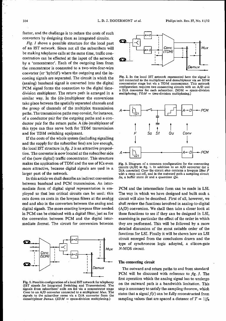
of an 1ST network. Since not all the subscribers willbe making telephone calls at the same time, traffic con-centration can be effected at the input of the networkby a 'concentrator'. Each of the outgoing lines fromthe concentrator is connected to a two-wire-four-wireconverter (or 'hybrid') where the outgoing and the in-coming signals are separated. The circuit in which the(analog) baseband signal is converted into the digitalPCM signal forms the connection to the digital time-division multiplexer, The return path is arranged in asimilar way. In the (de-)multiplexer the conversionstake place between the spatially separated channels andthe group of channels of the multiplex transmissionpaths. The transmission paths may consist, for instance,of a conductor pair for the outgoing paths and a con-ductor pair for the return paths. A (de-)multiplexer ofthis type can thus serve both for TDM transmissionand for TDM switching equipment.If the costs of the whole system (including signalling
and the supply for the subscriber line) are low enough,the local 1ST structure infig. 2 is an attractive proposi-tion. The converter is now located at the subscriber sideof the (now digital) traffic concentrator. This structuremakes the application ofTDM and the use oflCs evenmore attractive, because digital signals are used in alarger part of the network.In this article we shall describe an indirect conversion
between baseband and PCM transmission. An inter-mediate form of digital signal representation is em-ployed so that less critical circuits can be used: thiscuts down on costs in the lowpass filters at the analçgend and also in the converters between the analog anddigital signals. The more exacting lowpass filter neededin PCM can be obtained with a digital filter, just as forthe conversion between PCM and the digital inter-mediate format. The circuit for conversion between
Mux
Demux
Fig. 1. Possible configuration of a local 1ST network for telephony(1ST stands .for Integrated Switching and Transmission). Thesignals from subscribers' calls are fed via a concentrator stageCone to an AID converter connected to a multiplexer Mux. Thesignals to the subscriber come via a DIA converter from thedemultiplexer Demux. (SDM = space-division multiplexing.)
Fig. 2. In the local 1ST network represented here the signal isnot connected to the multipléxer and demultiplexer via an SOMconcentrator stage but via a TOM concentrator. This networkconfiguration requires two connecting circuits with an AID anda DIA converter for each subscriber. (SOM = space-divisionmultiplexing ; TDM = time-division multiplexing.)
A~ PCM
t t f t tF Sa st au Cony
! !A PCM
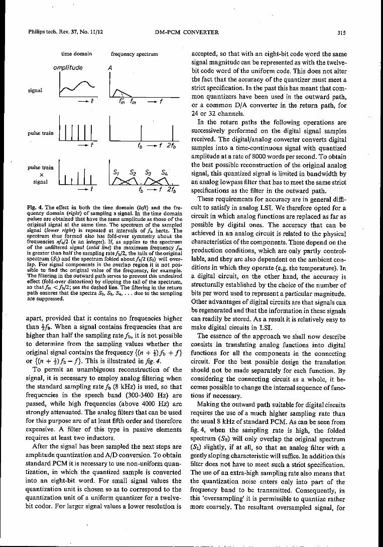
Fig. 3. Diagram of a common configuration for the connectingcircuits (AID) in fig. 1. In addition to an AID converter (or aDIA converter) Cony the circuit also contains a lowpass filter Fwith a steep cut-off, and in the outward path a sampling circuitSa, a buffer store St and a quantizer Qu.
PCM and the intermediate form can be made in LSI.The way in which we have designed and built such acircuit will also be described. First of all, however, weshall review the functions involved in analog-to-digital(AID) conversion. We shall then take a closer look atthese functions to see if they can be designed in LSI,examining in particular the effect of the order in whichthey are performed. This will be followed by a moredetailed discussion of the most suitable order of thefunctions for LSI. Finally it will be shown how an LSIcircuit emerged from the conclusions drawn and thetype of synchronous logic adopted, a silicon-gateN-MOS circuit.
The connecting circuit
The outward and return paths to and from standardPCM will be discussed with reference to fig. 3. Thefirst operation which the analog signal has to undergoon the outward path is a bandwidth limitation. Thisstep is necessary to satisfy the sampling theorem, whichstates that a signalf(t) can be fully reconstructed fromsampling values that are spaced a distance of T = llfb
Philips tech. Rev. 37, No. 11/12 DM-PCM CONVERTER 315
time domain frequency spectrum
signal a~ Alu~~'~' __-- t f/n fm -.. f
pulse train
pulse trainX
signal--t
Fig. 4. The effect in both the time domain (left) and the fre-quency domain (right) of sampling a signal. In, the time domainpulses are obtained that have the same amplitude as those of theoriginal signal at the same time. The spectrum of the sampledsignal (lower right) is repeated at intervals of /b hertz. Thespectrum thus formed also has fold-over symmetry about thefrequencies n/b/2 (n an integer). If, as applies to the spectrumof the unfiltered signal (solid line) the maximum frequency /mis greater than halfthe sampling rate/b/2, the tails oftheoriginalspectrum (SI) and the spectrum folded about/b/2 (S2) will over-lap. For signal components in the overlap region it is not pos-sible to find the original value of the frequency, for example.The filtering in the outward path serves to prevent this undesiredeffect (fold-over distortion) by clipping the tail of the spectrum,so that/m </b/2; see the dashed line. The filtering in the returnpath ensures that the spectra S2, S3, S4, ••• due to the samplingare suppressed.
apart, provided that it contains no frequencies higherthan tfb. When a signal contains frequencies that arehigher than half the sampling rate Ib, it is not possibleto determine from the sampling values whether theoriginal signal contains the frequency {en + t)/b + I}or {en + t)/b - f}. This is illustrated in fig. 4.To permit an unambiguous reconstruction of the
signal, it is necessary to employ analog filtering whenthe standard sampling rate fb (8 kHz) is used, so thatfrequencies in the speech band (300-3400 Hz) arepassed, while high frequencies (above 4000 Hz) arestrongly attenuated. The analog filters that can be usedfor this purpose are of at least fifth order and thereforeexpensive. A filter of this type in passive elementsrequires at least two inductors.
After the signal has been sampled the next steps areamplitude quantization and AID conversion. To obtainstandard PCM it is necessary to use non-uniform quan-tization, in which the quantized sample is convertedinto an eight-bit word. For small signal values thequantization unit is chosen so as to correspond to thequantization unit of a uniform quantizer for a twelve-bit coder. For larger signal values a lower resolution is
accepted, so that with an eight-bit code word the samesignal magnitude can be represented as with the twelve-bit code word of the uniform code. This does not alterthe fact that the accuracy of the quantizer must meet astrict specification. In the past this has meant that com-mon quantizers have been used in the outward path,or a common DIA converter in the return path, for24 or 32 channels.In the return paths the following operations are
successively performed on the digital signal samplesreceived. The digitalfanalog converter converts digitalsamples into a time-continuous signal with quantizedamplitude at a rate of 8000 words per second. To obtainthe best possible reconstruction of the original analogsignal, this quantized signal is limited in bandwidth byan analog lowpass filter that has to meet the same strictspecifications as the filter in the outward path.These requirements for accuracy are in general diffi-
cult to satisfy in analog LSI. We therefore opted for acircuit in which analog functions are replaced as far aspossible by digital ones. The accuracy that can beachieved in an analog circuit is related to the physicalcharacteristics ofthe components. These depend on theproduction conditions, which are only partly control-lable, and they are also dependent on the ambient con-ditions in which they operate (e.g. the temperature). Ina digital circuit, on the other hand, the accuracy isstructurally established by the choice of the number ofbits per word used to represent a particular magnitude.Other advantages of digital circuits are that signals canbe regenerated and that the information in these signalscan readily be stored. As a result it is relatively easy tomake digital circuits in LSI.The essence of the approach we shall now describe
consists in translating analog functions into digitalfunctions for all the components in the connectingcircuit. For the best possible design the translationshould. not be made separately for each function. Byconsidering the connecting circuit as a whole, it be-comes possible to change the internal sequence offunc-tions if necessary.Making the outward path suitable for digital circuits
requires the use of a much higher sampling rate thanthe usual 8 kHz of standard PCM. As can be seen fromfig. 4, when the sampling rate is high, the foldedspectrum (S2) will only overlap the original spectrum(SI) slightly, if at all, so that an analog filter with agently sloping characteristic will suffice.In addition thisfilter does not have to meet such a strict specification.The use of an extra-high sampling rate also means thatthe quantization noise enters only into part of thefrequency band to be transmitted. Consequently, inthis 'oversampling' it is permissible to quantize rathermore coarsely. The resultant oversampled signal, for

316 L. D. J. EGGERMONT et al. Philips tech. Rev. 37, No. 11/12
Fig. 6. Variant of the local 1ST network in fig. 2, in which the same intermediate code canbe used in both the outward and the return paths (see fig. 5). The method discussed in thisarticle is known as HIDM (High-Information Delta Modulation). The loop on the concen-trator indicates that in this circuit connections between subscribers connected to the sameconcentrator are made without the need for code conversion.
A PCM
PCMA
Fig. 5. Circuits for converting an analog signal (A) into a standardPCM signal (PCM) and vice versa for the outward and returnpaths in a local 1ST network of the type shown in fig. 2. Acharacteristic feature is the use of an intermediate code, whichrequires a digital code converter Cod Convat the PCM end. Inprinciple a separate intermediate code is possible for each of thetwo paths. The filter on the A side does not have to have a steepcut-off like the filter in fig. 3.
which a digital intermediate code is used, has to beconverted into 12-bit 8-kHz PCM. Obviously a digitallowpass filter is necessary to suppress signal compo-nents above 4 kHz. Finally the uniform 12-bit PCMhas to be converted into the non-uniform standard8-bit PCM.It is also desirable to use a less steep analog filter in
the return path. For reasons similar to those applicableto the outward path, this requires that the samplingrate Ib of the input signal to the analog filter should bemuch higher than follows from the sampling theorem,which says that t/b should be higher than the highestsignal frequency Im~When a high j], is used the spectraobtained from the original spectrum are so far apartthat a simple filter is sufficient to suppress them. Hereagain, the quantization noise enters into a broaderfrequency band than the band that contains the originalsignal spectrum. Consequently it is again permissible toquantize more coarsely, or to use fewer bits per word.A signal with a high j], for the return path can be ob-tained by means of a digital interpolating filter, whichcalculates the additional intermediate samples for thosesampling times of the intermediate code that do not
coincide with the sampling times ofthe 8-kHz standardPCM signal. This signal with high fb is digitally con-verted into an intermediate code with coarser quan-tization than in standard PCM.The resultant arrangement is shown in fig. 5. In prin-
ciple there is no restrietion on the choice of the inter-mediate codes for the outward and return paths. Thisallows the intermediate code for the outward path andthe code for the return path to be optimized separately.As shown infig. 6, however, attractive local 1ST struc-tures are possible if the same intermediate code is usedfor the outward and return path. The configurationshown has the advantage that only digital code con-verters are required for connections with other ex-
Mux
Demux
changes. The local connections are e~tablished in thecommon intermediate code via the TDM concentrator.In our circuit the sampling rate fb of the intermediatecode is 64 kHz, so that a simple second-order filter issufficient for both input and output. A special form ofdelta modulation called HIDM (High-InformationDelta Modulation) was chosen for the intermediatecode.In PCM the instantaneous value of the signal is coded
in digital form by the code words, but in delta modula-tion the difference between the present sampling valueand the reconstruction of the' previous sampling valueis coded in a one-bit code [11. The way in which thebit stream is calculated using HIDM is illustrated infig.7. An example of the structure of an HIDM en-coder is given in fig. 8. A major advantage of HIDMcompared with delta modulation with a continuously
. variable step size is that the step size can only assumevalues that are 2n (n a positive integer) times larger thanthe minimum step size. Since only these simple powersof 2 occur in the step-size control, digital decoding ofan HIDM signal is a relatively simple matter. Anotheradvantage of HIDM compared with ordinary delta
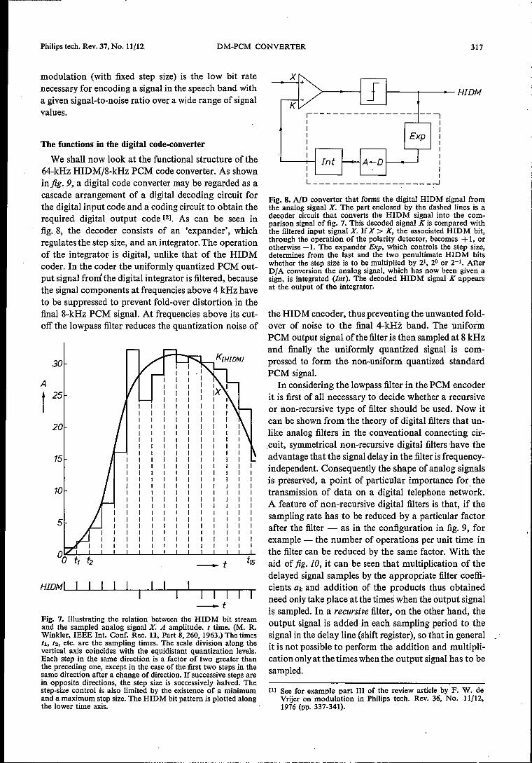
Philips tech. Rev. 37, No. 11/12. DM-PCM CONVERTER 317
modulation (with :fixed step size) is the low bit ratenecessar-yfor encoding a signal in the speech band witha given signal-to-noise ratio over a wide range of signalvalues.
The functions in the digital code-converter
We shall now look at the functional structure ofthe64-kHz HIDMj8-kHz PCM code converter. As showninfig. 9, a digital code converter may be regarded as acascade arrangement of a digital decoding circuit forthe digital input code and a coding circuit to obtain therequired digital output code [23. As can be seen infig. 8, the decoder consists of an 'expander', whichregulates the step size, and an integrator. The operationof the integrator is digital, unlike that of the HIDMcoder. In the coder the uniformly quantized PCM out-put signal from the digital integrator is filtered, becausethe signal components at frequencies above 4 kHz haveto be suppressed to prevent fold-over distortion in thefinal 8-kHz PCM signal. At frequencies above its cut-off the lowpass filter reduces the quantization noise of
A
t
-t
-tFig. 7. Illustrating the relation between the HIDM bit streamand the sampled analog signal X. A amplitude. t time. (M. R.Winkier, IEEE Int. Conf. Rec. 11, Part 8, 260, 1963.) The times11, tz, etc. are the sampling times. The scale division along thevertical axis coincides with the equidistant quantization levels.Each step in the same direction is a factor of two greater thanthe preceding one, except in the case of the first two steps in thesame direction after a change of direction. If successive steps arein opposite directions, the step size is successively halved. Thestep-size control is also limited by the existence of a minimumand a maximum step size. The HIDM bit pattern is plotted alongthe lower time axis.
!----y----+- HI DM
,---------------IIIIII
---,IIIIIIII
I IL ~
Fig. 8. AID converter that forms the digital HIDM signal fromthe analog signal X. The part enclosed by the dashed lines is adecoder circuit that converts the HIDM signal into the com-parison signalof fig. 7. This decoded signal K is compared withthe filtered input signal X. If X> K, the associated HIDM bit,through the operation of the polarity detector, becomes +1, orotherwise -1. The expander Exp, which controls the step size,determines from the last and the two penultimate HIDM bitswhether the step size is to be multiplied by 21, 2° or 2-1• AfterDIA conversion the analog signal, which has now been given asign, is integrated (Int). The decoded HIDM signal K appearsat the output of the integrator.
the HIDM encoder, thus preventing the unwanted fold-over of noise to the final 4-kHz band. The uniformPCM output signalof the filter is then sampled at 8 kHzand finally the uniformly quantized signal is com-pressed to form the non-uniform quantized standardPCM signal.
In considering the lowpass filter in the PCM encoderit is first of all necessary to decide whether a recursiveor non-recursive type of filter should be used. Now itcan be shown from the theory of digital filters that un-like analog filters in the conventional connecting cir-.cuit, symmetrical non-recursive digital filters "have theadvantage that the signal delay in the filter is frequency-independent. Consequently the shape of analog signalsis preserved, a point of particular importance for. thetransmission of data on a digital telephone network.A feature of non-recursive digital filters is that, if thesampling rate has to be reduced by a particular factorafter the filter - as in the configuration in fig. 9, forexample - the number of operations per unit time inthe filter can be reduced by the same factor. With theaid of fig. 10, it can be seen that multiplication of thedelayed signal samples by the appropriate filter coeffi-cients ak and addition of the products thus obtainedneed only take place at the times when the output signalis sampled. In a recursive filter, on the other hand, theoutput signal is added in each sampling period to thesignal in the delay line (shift register), so that in generalit is not possible to perform the addition and multipli-cation only at the times when the output signal has to besampled.
[1] See for example part III of the review article by F. W. deVrijer on modulation in Philips tech. Rev. 36, No. 11/12,1976 (pp. 337-341).
318 L. D. J. EGGERMONT et al. Philips tech. Rev. 37, No. 11/12
r---------------,t-+I-t_+:_, ~PCM
1 I1 ~L ~ L ~HIDM Dec PCM Ene
Fig.9. Operating principle ofthe HIDM-PCM code converter. The two blocks in the dashedrectangle on the left (HIDM Dec) convert the HIDM code into a non-standard uniformPCM signal. The two blocks on the right (PCM Ene) make a standard PCM signal from thiscode. Exp expander. Int integrator. Compr digital compressor. The sampler is denoted by theswitch symbol. This is preceded by a digital filter.
Constructing a sequence of functions suitable for LSI
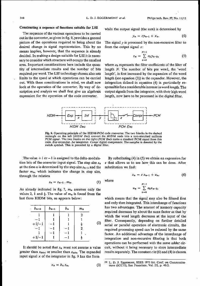
The sequence of the various operations to be carriedout in the converter, as given in fig. 9,"provides a generalpicture of the operations required to bring about thedesired change in signal representation. This by nomeans implies, however, that the sequence is alreadydecided. In making a design suitable for LSI it is neces-sary to consider which structure will occupy the smallestarea. Important considerations here include the quan-tity of intermediate results and the number of bitsrequired per word. The LSI technology chosen also setslimits to the speed at which operations can be carriedout. With these considerations in mind, we shall nowlook at the operation of the converter. By way of de-scription and analysis we shall first give an algebraicexpression for the operation of the code converter.
HIDM
.The value +1or -1 is assigned to the delta-modula-tion bits of the converter input signal. The step size Snat the time n is determined by the step size Sn-l and thefactor m«, which indicates the change in step size,through the relation
Sn = Sn-l . mn.
As already indicated in fig. 7, m« assumes only thevalues 2, 1 and t. The value of m« is found from thelast three HIDM bits, as appears below:
bn-2 bn-l bn mn
1 1 1 2-1 1 1 1
+1/-1 -1 1 t-1 -1 -1 21 -1 -1 1
+1/-1 1 -1 t
It should be noted that Sn must not assume a valuegreater than Smax or smaller than Smin. The expandedinput signal x of the integrator in fig. 9 has the form
Xn = b« Sn,
while the output signal (the sum) is determined by
Yn = CYn-l + Xn. (4)
The signal Y is processed by the non-recursive filter toform the output signal z:
N-l
Zn = L asy«-»,k=O
where ak represents the filter coefficients of the filter oflength N. The number of bits per word, the 'wordlength', is first increased by the expansion of the wordlength (see equation (3» in the expander. However, theintegration defined in equation (4) is particularly re-sponsible for a considerable increase in word length. Theoutput signals from the integrator, with their high wordlength, now have to be processed in the digital filter.
(5)
By substituting (4) in (5) we obtain an expression forZ that allows us to see how this can be done. Aftersubstitution we find:
Zn = CZn-l + Un, (6)
(1) whereN-l
Un = L aex»-»,k-O
(2)
which means that the signal mayalso be filtered firstand only then integrated. This interchange of functionshas two advantages. The amount of memory capacityrequired decreases by about the same factor as that bywhich the word length decreases at the input of thefilter. Consequently, depending on further detailedserial or parallel operation of electronic circuits, therequired processing speed can be reduced by the samefactor. An additional advantage of the interchange ofintegration and non-recursive filtering is that bothoperations can be. performed with the same adder cir-cuit, without it being necessary to store intermediateresults separately. The constant C irr(ö) and (4) is chosen
(3)(2) L. D. J. Eggermont, IEEE 1975 Int. Conf. on Communica-
tions (ICC75), San Francisco, Vol. Ill, p. 40.2.

Philips tech. Rev. 37, No. 11/12 DM-PCM CONVERTER 319
Fig. 10. A symmetrical non-recursive digital filter and the analog equivalent of its digitalpulse response. The operation can be described as the addition of input-signal samples multi-plied by fixed factors. The input signal Vi undergoes successive delays of T (in this case fourtimes). After-each delay it is multiplied by a fixed factor aj. The sum of the (four) productsand aD times the non-delayed signal is the output signal Voo
in such a way that a simple electronic circuit can beused. The expression chosen was
which only requires a shift and subtraction operation.The constant c was made less than 1 because the stabil-ity of the integrator is then guaranteed. The exponent pwas made fairly large because this offers a good ap-proximation to the integration (c = 1).Apart from this interchange of integration and filter-
ing, it is also possible to limit the size of the memorycapacity required by including the step-size control forthe expander in the filter. It is not then necessary tohold the step-size words x, ail that need be stored arethe HIDM bits and an initial step-size value, so thatthe memory can be about eight times smaller. The step
size then has to be calculated for every shift-and-addoperation, of course. But since the calculation of thestep size from the bit stream, using equations (2) and(3), can run in parallel with the multiplications in thefilter the incorporation of the step-size control in thefilter has no effect on the processing speed, nor on theamount of electronics required.
The processing rate required for the filter can besubstantially reduced because only one out of everyeight samples need be calculated. We shall now lookfirst at the interchange of integration and samplingnecessary here. In the case of a reduction in the samp-ling rate at the input of the integrator by a factor R,equation (6) yields
R-l
ZnR = CRZ(n-l)R + L: ctunR_I. (8)1=0
In terms of actual electronic circuits, this equationmeans that a non-recursive filter with filter coefficients
(7)
et, separated by a sampler, precedes an integrator withthe constant cR. This interchange of integration andreduction in the sampling rate does not in itself giveany advantage. But since the non-recursive. filter, noweven more necessary, can be combined with the existingnon-recursive filter, an advantage is nevertheless ob-tained. The original non-recursive filter is expanded byR - 1 sections. The filter coefficients a' k of this modi-fied lowpass filter are obtained by substituting u (seeequation (6)) in (8):
R-l
a' k = L: ctak-t,1=0
(9)
in which the unmodified filter coefficients am with msmaller than zero or greater than N - 1 are assumed
to be equal to zero. From the above we see that theinterchange of integrator and sampler leads to an in-crease in the filter length from N to N + R - 1; weshall call this length N'.Now let us look at the interchange of the filter and
reduction of sampling rate. This interchange, whichgives a reduction in the required processing rate, as wesaw earlier, also leads to a reduction in the number ofsamples that have to remain stored in the filter forcalculating the next output sample. Without any reduc-tion in sampling rate (R = 1) it is now necessary tostore N' - 1 samples in the modified filter of length N'.For reduction factors greater than 1 but smaller thanN', at least N' - R samples must be stored in the filterfor calculating the next output sample, whereas withvalues of R greater or equal to N' the next output signalis determined entirely by the samples arriving after theprevious calculation. In this case, therefore, the filterdoes not need to retain any earlier sample value at allfor the next calculation period [31. The final result of

320 L. D. J. EGGERMONT et al. Philips tech. Rev. 37,No. 11/12
positioning the sampling reduction R before the filter-ing and integration stages is shown in fig. 11. Thecomplete process of changing the sequence of thevarious operations is again summarized in fig. 12.
N-11--------Nmin
t2NN
-RFig. 11. The minimum number of samples Nmin that must bestored in a filter is N - 1 for each value of the sampling reduc-tion R. N is the length of the unmodified filter.
between the parallel read-in ofthe R (= 8) HIDM bits,this register always shifts eight steps 'too far'. Thisleads to the desired situation in which, when the R newHIDM bits are input, the R oldest bits are transferred.At the same time, at the beginning of every calculationperiod in the filter, the step size stored for the previousone must be input to the expander. After R clock pulsesthe resultant step size is then stored for the next cal-culation period in the filter. This has to be done afterR clock pulses (= shift pulses) because the bit at thelocation N - R, immediately after read-in of the RHIDM bits in the one calculation period has to arriveat location N at the beginning of the next one.
HIDM PCM
HIDM PCM
HIDM PCM
HIDM PCM
PCM
HIDM--4 _/_ + F + Exp 1-1---11Int; CIi'II----11 Compr ~ PCM
Fig. 12. Diagram showing the various steps in deriving a structure suitable for LSI from thediagram of fig. 9. The first step permits a smaller word length to be used in the filter. Thesecond step, which limits the number of operations in the integrator, shows that the inter-change of integrator and sampler leads to the introduetion of an extra filter and to a changein the integration constant. In the third step these filters are combined, and the fourth stephas the effect of reducing the number of operations in the filter. The last step is responsiblefor word-length expansion in the lowpass filter.
Block diagram of code converter
In circuits intended for telephony the dissipationshould not be unduly high, and an integrated circuitshould not therefore be required to operate at very highspeeds if it can be avoided. For this reason we decidedagainst serial operation for the digital signal processor,and chose parallel operation. The block diagram of thesignal processor with the structure given in fig. 12 isshown in fig. 13 [4]. This converter comprises a filterwith 100 sections. The shift register belonging to thefilter has 120 sections. Since there are 128 clock pulses
The multiplications of the filter coefficients by thestep size of 2n required for the filtering is achieved byshifting each filter coefficient by n places. The shiftedfilter coefficients - i.e. multiplied by a power oftwo -are then added in the accumulator, taking the signs intoaccount. These nine-bit filter coefficients are stored ina 50-word ROM (read-only memory). The 50-wordROM is sufficient since only 50 different filter coeffi-cients are required for the symmetrical non-recursivedigital filter chosen. This implies that for the filter - butnot for the integration - the constant c in (9) is made
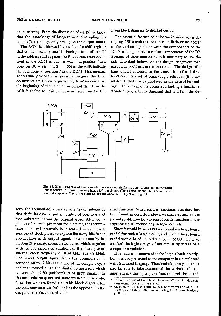
Philips tech. Rev. 37, No. 11/12 DM-PCM CONVERTER 3~1
Fig. 13. Block diagram of the converter. An oblique stroke through a connection indicatesthat it consists of more than one line. Muit multiplier. Comp complement. Ace accumulator.s initial step size. The other symbols are the same as in fig. 9 and fig. 11.
equal to unity. From the discussion of eq. (9) we knowthat the interchange of integration and sampling hassome effect (though only small) on the output signal.The ROM is addressed by means of a shift register
that contains exactly one '1'. Each position of this '1'in the address shift register, ASR, addresses one coeffi-cient in the ROM in such a way that position i andposition 101- i (i = 1, 2, ... 50) in the ASR indicatethe coefficient at position i in the ROM. This unusualaddressing procedure is possible because the filtercoefficients are always required in afixed sequence. Atthe beginning of the calculation period the '1' in theASR is shifted to position 1. By not resetting itself to
zero, the accumulator operates as a 'leaky' integratorthat shifts its own output a number of positions andthen subtracts it from the original word. After com-pletion ofthe multiplications for the filter, the accumu-lator - as will presently be discussed - requires anumber of clock pulses to express the carry bits in theaccumulator in its output signal. This is done by in-cluding 28 separate accumulator pulses which, togetherwith the 100 associated additions of the filter, give aninternal clock frequency of ]024 kHz (128 x 8 kHz).The 20-bit output signal from the accumulator isrounded off to 12 bits at the end of the complete cycleand then passed on to the digital compressor, whichconverts the 12-bit (uniform) PCM input signal intothe non-uniform quantized standard 8-bit PCM code.Now that we have found a suitable block diagram forthe code converter we shalliook at the approach to thedesign of the electronic circuits.
From block diagram to detailed design
The essential feature to be borne in mind when de-signing LSI circuits is that there is little or no accessto the various signals between the components of theIC. Nor it is possible to replace components of the IC.Because of these constraints it is necessary to use theaids described below. As the design progresses twoparticular problems are encountered. The design of alogic circuit amounts to the translation of a desiredfunction into a set of binary logic relations (Booleanrelations) that can be produced in the desired technol-ogy. The first difficulty consists in finding a functionalstructure (e.g. a block diagram) that will fulfil the de-
PCM
sired function. When such a functional structure hasbeen found, as described above, we come up against thesecond problem - howto reproduce its functions in theappropriate IC technology in logic circuits.
Since it would be no easy task to make a breadboardmodel for such a lar-gecircuit, and since a breadboardmodel would be of limited use for an MOS circuit, wechecked the logic design of our circuit by means of a .computer simulation.This means of course that the logic-circuit descrip-
tion must be presented to the computer in a simple andwell structured language. The simulation program mustalso be able to take account of the variations in theinput signals during a given time interval. From this
[3J In fact, because of the relation between N' and R, this situa-tion cannot occur in the system.
[4J G. P. Edwards, T. Preston, L. D. J. Eggermont and M. H. H.Höfelt, 1976 Int. Zürich Seminar on Digital Communications,p. B 3.1.

\
322 L. D. J. EGGERMONT et al. Philips tech. Rev. 37, No. 11/12
data relating to the structure and the input signals thesimulation program determines the signal at the outputsand also a number of internal signals. The method isvery versatile. Input signals can easily be changed. Thelogic design can also be modified quickly and easily ifthe result ofthe simulation shows that it is necessary.For the simulation, the use of clocked or synchron-
ous logic has considerable advantage over asynchron-ous logic, because the number of possible timing rela-tions between the signals from a particular part of thecircuit is very much smaller with synchronous logic.This means that simulation with this type of logic canbe much faster and more reliable than with asynchron-ous logic. Largely for this reason we decided to usesynchronous logic for the converter.An important aspect to be considered in any design
is the extent to which the IC resulting from a givendesign can be tested by finding the output signal as-sociated with a given input signal. We do this by usingthe simulation program that works from a circuit de-scription to which 'faults' have been added. With thisdescription it is possible to see which gates are testedand which are not for any given input signal. This pro-cedure is called test verification. Ifthe result is not satis-factory, the designer may decide that either the use ofadditional (or different) test signals or the modificationof the design would give successful testing. At an earlystage in the design the problems of testing should bethoroughly examined, especially since there are somecategories of circuit that are very difficult to test, inwhich a small modification can greatly facilitate thetesting.When using the test program or the simulation pro-
gram it is necessary to know the output signal thatshould be obtained for a given input signal. Here weused a simulation program that does not work at 'gatelevel', like the one just described, but describes com-plete digital functional units (e.g. shift registers, accu-mulators and memories), without taking the internalstructure of these units into account. The desired rela-tion between the HIDM input signal and the PCM out-put signalof the digital code converter was determinedwith this block-simulation program with the aid of theblock diagram shown in fig. 13.If a breadboard model is used, characteristics such as
quantization noise and the subjective perception can bedetermined in a simple way. But if it is not thought de-sirable to make a breadboard model, these character-istics will have to be determined from a simulationprogram. The gate-level simulator is not so suitable forthis purpose, since it is not fast enough to simulate afew seconds of speech processing in the code converter.We have therefore also used the block-level simulatorfor: these determinations.
Electronic design and technology
In the previous section we have described how wearrived at a block diagram for the digital code con-verter. Next we saw how the program simulating theoperation of that block diagram and the gate-levelsimulation were used and compared with each other.We shall now discuss the four-phase dynamic MOSlogic used in the converter.
Four-phase dynamic MOS logic
A circuit based on four-phase dynamic MOS logic isshown in fig. 14. The charge state of the capacitor Cldetermines the value ('true' or 'not true') of the Booleanfunction f The value of f is arrived at as follows. Intime interval1 the capacitor Cl is charged via Tl as aresult of the clock pulse epI. During the next time inter-val2 the value of epI is zero, but ep2 keeps T2 conducting.Thus, Cl is discharged if there is a conducting pathpresent in the logic circuit Logi, This conducting con-nection occurs when the logic function a (b + c) + dehas the value 'true' [51.In this case Cl discharges, andthe charge (and the potential) of Cl represents thefunction f = a(b + c) + de. The logic values formedin this manner remain in position until the next epIpulse arrives, and can therefore be used as a reliableinput signal for logic networks-with type-3 gates, whichare driven by the clock pulses ~3 and ep4 - in the sameway as networks with type-l gates are driven by theclock pulses epI and ep2. At the output a function gappears, which is represented by the state of charge ofC2. In their turn the output values of type-3 gates arestable during clock pulses epI and ep2, and are thussuitable for driving type-l gates.
In addition to these two important types of gatethere are also type-2 and type-4 gates. A slightly sim-plified configuration of a type-2 gate can be seen at thetop ofthe circuit in fig. 14. The capacitor C3 here con-tains the inverse off. In time interval1 capacitor C3 isfirst charged via T5 and then discharged via T6 at thebeginning of time interval 3. Now type-3 gates onlyrequire their logic input signals during time interval 4.As a result, type-2 gates deliver their output signal tothe input of the type-3 gates at exactly the right time.
One advantage of separating the various operationsinto time intervals is that the dimensions and physicalcharacteristics of the transistors do not have to be socritical for the circuits to function properly. Since anytransistor can in principle be used in this configuration,the smallest transistor permitted by the technology willin general be used, provided the speed requirementsallow it. Since it is. also possible to achieve a fairlycomplicated function per gate, a high packing densitycan be obtained. It is often unnecessary to use flip-flops,since the charged capacitors perform their function.

Philips tech. Rev. 37, No. 11/12 DM-PCM CONVERTER
Another virtue of four-phase logic is its low power,because there is no standing d.c. current. The circuitdiscussed here requires only 15 mW.
The circuit was made with an MOS process using theLOCOS field-oxide technology, which is based on athick buried oxide layer. In this technology the tran-
rp,
rp,
rp2
<1>3 r=.rp4, / \
1 2 3 4
Qbc
de
'-- ---J!
'--- ....J!2 3
=EJ-AND
=B-aR
I IL_J _JLog2
CP3
r r----'I
:L092~I~
'------+- I 3L _J
Fig. 14. Illustrating the operation of four-phase dynamic MOS logic. From top to bottom:a circuit, the four series of clock pulses rfo and the logical representation of the circuit, a, b,e, d and e are arbitrary digital input signals. Logl, Log2 logic circuits. In the logical represen-tation the gates of the various types are denoted by the appropriate digit. These gates areeasily identified in the circuit.
It is necessary to check carefully, and separately from thesimulation, whether the information stored in the IC as a chargeon a capacitor might not be degraded on account of parasiticcapacitances at crossings between the conductor connected to itand other connectors. If the parasitic capacitance to crossinglines is found to be too high compared with the buffer capacitanceof the IC, the buffer capacitance must be increased.
=ErInv
sistors and the interconnections - which lie on thethick LOCOS oxide - have low parasitic capacitances.This allows fast circuits to be made that require
[5] a(b + c) + de means: a and (b or c) or (d and e). This func-tion has the value 'true' if (a and b) and/or (a and c) and/or(d and e) are true.
323

324 L. D. J. EGGERMONT et al. Philips tech. Rev. 37, No. 11/12
,,'---- ..
•
Philips tech. Rev. 37, No. 11/12 DM-PCM CONVERTER,325
relatively little power. The desired clock frequencty(1.024 MHz) presents no problems. I
In this technology, interconnections can be eitherdiffused polysilicon or metal. Although a diffused inter-connection and a polysilicon one cannot cross eachother, it is very useful to have three kinds of intercon-nection available. Even with conservative layout rulesfor spacings and dimensions, a density of 200 NAND-gate-equivalents/mmê could be obtained with thistechnology.
Design of the layout
Our approach for the design of the layout could bedescribed as semi-automated. The computer performsoperations such as displacement, repetition and rota-tion of the patterns, but the structure of the layout isworked out by the designer and then supplied to theprogram.
One ofthe advantages ofthe semi-automated methodis that a higher packing density can be obtained. This isbecause there are more degrees of freedom available.For the same reason, it is easier to optimize the pro-cessing speed for this circuit.. Since the circuit has high regularity, a fully automat-ed method would not save much time compared withthe semi-automated one. A disadvantage of the methodwe have chosen is that it is more difficult to check thecorrectness of the layout than with a fully automatedprocedure.
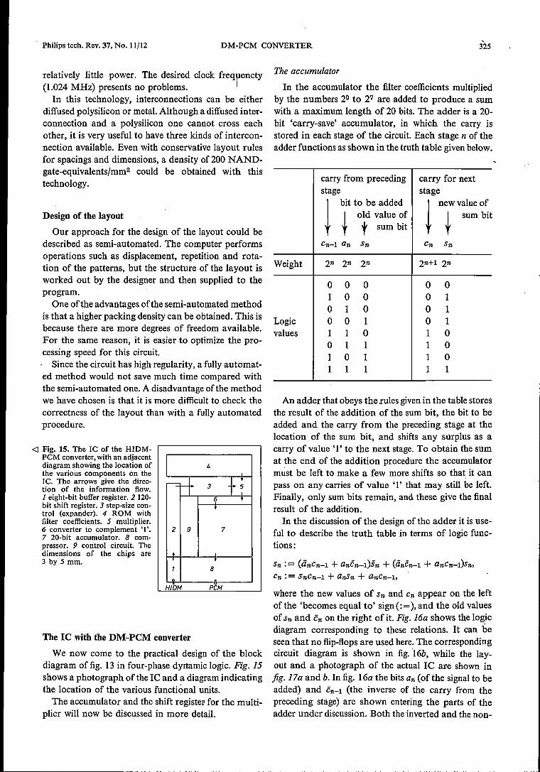
<l Fig. IS. The IC of the HIDM-PCM converter, with an adjacentdiagram showing the location ofthe various components on theIC. The arrows give the direc-tion of the information flow.1 eight-bit buffer register. 2 120-bit shift register. 3 step-size con-trol (expander). 4 ROM withfilter coefficients. 5 multiplier.6 converter to complement '1'.7 20-bit accumulator. 8 com-pressor. 9 control circuit. Thedimensions of the chips are3 by 5 mm.
4
--=-t 3 +;6 t
t
2 9 7
+t
1 8
" .HID"" PC""
The IC with the DM-PCM converter
We now come to the practical design of the blockdiagram offig. 13 in four-phase dynamic logic. Fig. 15shows a photograph of the IC and a diagram indicatingthe location of the various functional units.
The accumulator and the shift register for the multi-plier will now be discussed in more detail.
The accumulator
In the accumulator the filter coefficients multipliedby the numbers 2° to 27 are added to produce a sumwith a maximum length of 20 bits. The adder is a 20-bit 'carry-save' accumulator, in which the carry isstored in each stage of the circuit. Each stage n of theadder functions as shown in the truth table given below.
carry from preceding carry for nextstage stage
tbit to be added ~ new value of
t old value of t sum bit
t sum bit
Cn-l an Sn Cn Sn
Weight 2n 2n 2n 2n+l 2n
0 0 0 0 01 0 0 0 10 1 0 0 1
Logic 0 0 1 0 1values 1 1 0 1 0
0 1 1 1 01 0 1 1 01 1 1 1 1
An adder that obeys the rules given in the table storesthe result of the addition of the sum bit, the bit to beadded and the carry from the preceding stage at thelocation of the sum bit, and shifts any surplus as acarry ofvalue '1' to the next stage. To obtain the sumat the end of the addition procedure the accumulatormust be left to make a few more shifts so that it canpass on any carries of value '1' that may still be left.Finally, only sum bits remain, and these give the finalresult of the addition.
In the discussion of the design of the adder it is use-ful to describe the truth table in terms of logic func-tions:
Sn := (änCn-l + anén-l)Sn + (tinén-l + anCn-l)Sn,Cn := SnCn-l + anSn + anCn-l,
where the new values of Sn and Cn appear on the leftof the 'becomes equal to' sign (: =); and the old valuesof Sn and én on the right of it. Fig. 16a shows the logicdiagram corresponding to these relations. It can beseen that no flip-flops are used here. The correspondingcircuit diagram is shown in fig. 'I6b, while the lay-out and a photograph of the actual IC are shown injig. 17a and b. In fig. 16a the bits an (ofthe signal to beadded) and én-l (the inverse of the carry from thepreceding stage) are shown entering the parts of theadder under discussion. Both the inverted and the non-

326 L. D. J. EGGERMONT et al. Philips tech. Rev. 37, No. 11/12
inverted signal are produced from these two signals ina type-l and a type-2 inverter. At the same time, type-land type-2 inverters form Sn and Sn from the previous
In the case where an and Cn-I are zero, the part ofthe circuit drawn in heavy lines forms a hold circuitfor Sn. A circuit of this type is a very simple structure
an
2 1 1 2
a ën-l an ën
Sn
</>3 </>3
</>,
</>4
</>2
ën-l
</>3
</>1
b an
Fig. 16. The logic diagram (a) and the circuit (b) of a stage of the 'carry-save' accumulator(Acc in fig. 13). The types of gate used in four-phase logic are denoted by the appropriatedigit. If an and the carry Cn-l are zero, the part of the circuit drawn in heavy lines forms ahold circuit for the sum bit Sn. In the two diagrams corresponding functions are locatedat the same place, where possible.
value of Sn. The six signals thus formed, an, än, en-I,én-I, Sn and Sn, arrive next at the input of two type-3gates. The new sum bit is formed in the left-hand type-3gate, while the new carry is produced by the right-handtype-3 gate.
which could be said to be inherent in four-phase logic.The IC contains the transistors at the locations where
polysilicon crosses a diffusion path (black squares infig. 17a).As can beseeninfig.17b, theinterconnectionsare either of aluminium (shown bright in the photo-

Philips tech. Rev. 37, No. 11/12 DM-PCM CONVERTER
-~- ---
--- -- --
r-r-r-: ~ ~0 ~ 0 o~~ ,-- ~-.::o -
c::: I .- _j- LI ]
=~
0 0 .8Ot0 0 ~r-'
0 0 DI_jr..J
~~
ID 0 0~
I 1110 0IIr!-
0 :I r-"O~~ 0
'-t L___f-0 0 0~oJII - r= ~ 0
-1""1-' =-- ++Or - c-----,O L.J 0'-=' c=J ---=
0
/',Fig. 17. a) The layout of the ac-cumulator stage of fig. 16. Thealuminium interconnections,mainly horizontal, are outlinedin blue, and the polysilicon inter-connections are shown in red.The diffusion channels lie insidethe grooves in the thick oxide,marked green. Places wherepolysilicon covers the diffusionchannel mark the location of anMOS (enhancement) transistor(black squares). No N-type dop-ant will penetrate into the chan-nel at these locations. All partsof the channels not covered bypolysilicon, on the other hand,receive N-type doping. The con-tact openings of the aluminiumwith the underlying material(polycrystalline silicon or siliconin the openings in the oxide) areoutlined in black. At some posi-tions where polysilicon crossesthe diffusion channel an elec-trical contact between the two isreq uired rather than a transis-tor. Here again, a special con-tact window is required; itsopenings are also outlined inblack. b) Photograph of the ac-cumulators on the chip. The lightaluminium tracks are easily re-cognized, and so too are thepolysilicon interconnections(mainly vertical). The diffusedchannels can be recognized fromtheir dark edges.
a b
00 al 02
<PI
<P2
5352SI
So
Fig. 18. a) Circuit diagram of asimplified model of the multiplier.b) The circuit of the multiplier isdrawn in a similar manner to thatof the layout. The horizontal linesSO'S3 are polysilicon in the IC. Theseinterconnections cross the verticalaluminium tracks, which are showndashed in the figure.
327
328 L. D. J. EGGERMONT et al. Philips tech. Rev. 37, No. 11/12
a
Fig.19. a) Layout of the logic circuit for the multiplier. The colours have the same significaneeas in fig. 17a. The circuit for n-r is shown in grey. b) Photograph of the multiplier sectionof the IC. The various structures can be recognized with reference to the layout in (a). Thediffusion channels can be identified by their dark edges.
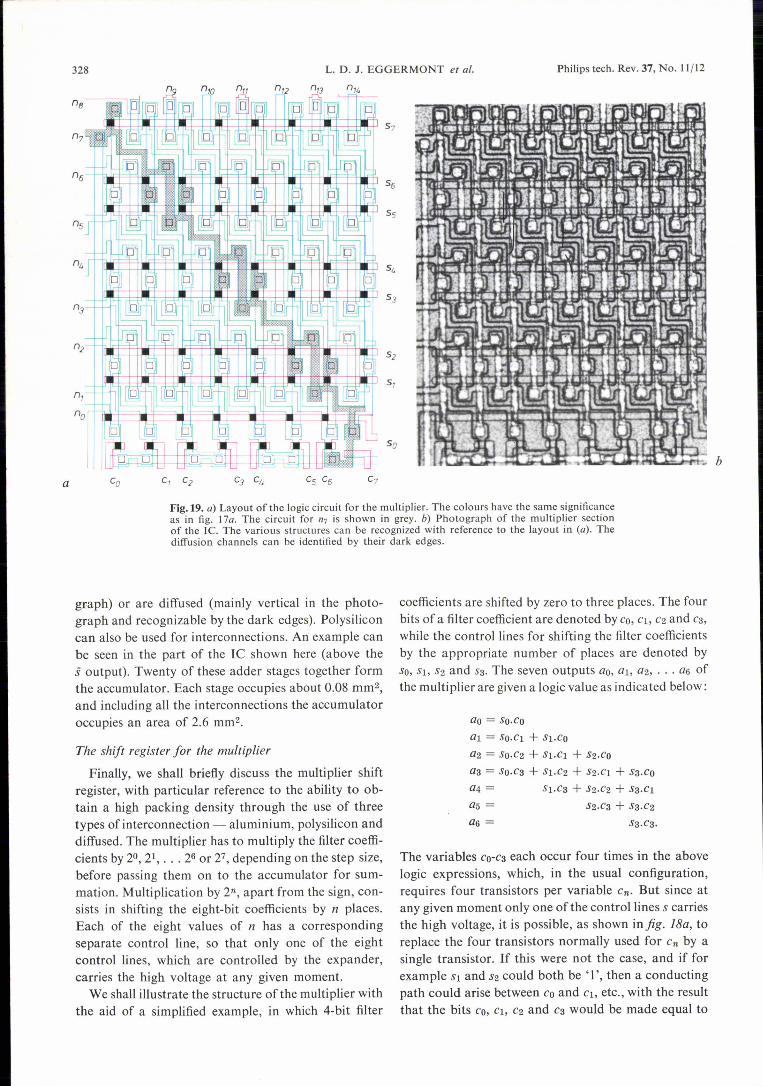
graph) or are diffused (mainly vertical in the photo-graph and recognizable by the dark edges). Polysiliconcan also be used for interconnections. An example canbe seen in the part of the IC shown here (above thes output). Twenty of these adder stages together formthe accumulator. Each stage occupies about 0.08 mm-,and including all the interconnections the accumulatoroccupies an area of 2.6 mm".
The shift register for the multiplier
Finally, we shall briefly discuss the multiplier shiftregister, with particular reference to the ability to ob-tain a high packing density through the use of threetypes ofinterconnection - aluminium, polysilicon anddiffused. The multiplier has to multiply the filter coeffi-cients by 20, 21, ••. 26 or 27, depending on the step size,before passing them on to the accumulator for sum-mation. Multiplication by 2n, apart from the sign, con-sists in shifting the eight-bit coefficients by n places.Each of the eight values of n has a correspondingseparate control line, so that only one of the eightcontrol lines, which are controlled by the expander,carries the high voltage at any given moment.
We shall illustrate the structure ofthe multiplier withthe aid of a simplified example, in which 4-bit filter
coefficients are shifted by zero to three places. The fourbits of a filter coefficient are denoted by Co, Cl, C2 and C3,
while the controllines for shifting the filter coefficientsby the appropriate number of places are denoted byso, st, S2 and S3. The seven outputs ao, al, a2, ... a6 ofthe multiplier are given a logic value as indicated below:
ao = So.Co
al = SO.Cl + Sl.CO
a2 = SO·C2 + Sl.Cl + S2.CO
a3 = SO.C3 + Sl.C2 + S2.Cl + S3.CO
a4 = Sl.C3 + S2.C2 + S3.C1
a5 = S2.C3 + S3.C2
The variables CO-C3 each occur four times in the abovelogic expressions, which, in the usual configuration,requires four transistors per variable Cn. But since atany given moment only one ofthe controllines S carriesthe high voltage, it is possible, as shown infig. I8a, toreplace the four transistors normally used for Cn by asingle transistor. If this were not the case, and if forexample Sl and S2 could both be '1', then a conductingpath could arise between Co and Cl, etc., with the resultthat the bits Co, Cl, C2 and C3 would be made equal to

Philips tech. Rev. 37, No. 11/12 DM-PCM CONVERTER 329
one another. This danger does not exist here, however.The compact structure permitted by the use of threetypes of interconnection is shown in fig. ISb, the layoutof the multiplier is shown in fig. 19a, and fig. 19b showsthe final circuit, with an area of 0.25 mmê.Our objectives, arising from the requirements for an
1ST system, have thus been achieved: to structure thearchitecture of a digital code converter in such a waythat the design would be suitable for LSI, and then tofabricate the circuit in the form of LSI hardware.
Summary. The development of LSI circuits makes it possible touse digital techniques in a telephone network, both for trans-mission and for switching. This can have considerable economicadvantages, provided the analog/digital and digital/analog con-verters are inexpensive. This implies that the usè of expensiveanalog filters has to be avoided. The article describes an A/Dconverter in which the analog signals are indirectly convertedinto the standard PCM code via an HIDM code ('High-Informa-tion Delta Modulation'). It is shown how the conversion of thisintermediate code into the PCM code can be resolved into itselementary functions and subsequently combined so as to producea design suitable for fabrication as an LSI circuit. A descriptionis given of the design of the circuit in an LSI technology thatcombines a high packing density with low dissipation. The tech-nology used is four-phase dynamic MOS logic.