address bus data bus control and status signals
TRANSCRIPT

EDAYATHANGUDY G.S PILLAY ARTS AND SCIENCE COLLEGE, NAGAPATTINAM-611002
PG AND RESEARCH DEPARTMENT OF PHYSICS
MICROPROCESSOR - 8085
The following image depicts the pin diagram of 8085 Microprocessor −
Address bus
A15-A8, it carries the most significant 8-bits of memory/IO address.
Data bus
AD7-AD0, it carries the least significant 8-bit address and data bus.
Control and status signals

These signals are used to identify the nature of operation. There are 3 control signal and 3 status signals.
Three control signals are RD, WR & ALE.
RD − This signal indicates that the selected IO or memory device is to be read and is ready for accepting data available on the data bus.
WR − This signal indicates that the data on the data bus is to be written into a selected memory or IO location.
ALE − It is a positive going pulse generated when a new operation is started by the microprocessor. When the pulse goes high, it indicates address. When the pulse goes down it indicates data.
Three status signals are IO/M, S0 & S1.
IO/M
This signal is used to differentiate between IO and Memory operations, i.e. when it is high indicates IO operation and when it is low then it indicates memory operation.
S1 & S0
These signals are used to identify the type of current operation.
Power supply
There are 2 power supply signals − VCC & VSS. VCC indicates +5v power supply and VSS indicates ground signal.
Clock signals
There are 3 clock signals, i.e. X1, X2, CLK OUT.
X1, X2 − A crystal (RC, LC N/W) is connected at these two pins and is used to set frequency of the internal clock generator. This frequency is internally divided by 2.
CLK OUT − This signal is used as the system clock for devices connected with the microprocessor.
Interrupts & externally initiated signals
Interrupts are the signals generated by external devices to request the microprocessor to perform a task. There are 5 interrupt signals, i.e. TRAP, RST 7.5, RST 6.5, RST 5.5, and INTR. We will discuss interrupts in detail in interrupts section.
INTA − It is an interrupt acknowledgment signal.

RESET IN − This signal is used to reset the microprocessor by setting the program counter to zero.
RESET OUT − This signal is used to reset all the connected devices when the microprocessor is reset.
READY − This signal indicates that the device is ready to send or receive data. If READY is low, then the CPU has to wait for READY to go high.
HOLD − This signal indicates that another master is requesting the use of the address and data buses.
HLDA (HOLD Acknowledge) − It indicates that the CPU has received the HOLD request and it will relinquish the bus in the next clock cycle. HLDA is set to low after the HOLD signal is removed.
Serial I/O signals
There are 2 serial signals, i.e. SID and SOD and these signals are used for serial communication.
SOD (Serial output data line) − The output SOD is set/reset as specified by the SIM instruction.
SID (Serial input data line) − The data on this line is loaded into accumulator whenever a RIM instruction is executed.
Registers of 8085 microprocessor
A microprocessor is a multipurpose, programmable, clock-driven, register-based electronic device that reads binary instructions from a storage device called memory, accepts binary data as input and processes data according to those instructions and provide results as output. A 8085 microprocessor, is a second generation 8-bit microprocessor and is the base for studying and using all the microprocessor available in the market. Registers in 8085: (a) General Purpose Registers –
The 8085 has six general-purpose registers to store 8-bit data; these are identified as- B, C, D, E, H, and L. These can be combined as register pairs – BC, DE, and HL, to perform some 16-bit operation. These registers are used to store or copy temporary data, by using instructions, during the execution of the program.
(b) Specific Purpose Registers –
Accumulator: The accumulator is an 8-bit register (can store 8-bit data) that is the part of the arithmetic and logical unit (ALU). After performing arithmetical or logical operations, the result is stored in accumulator. Accumulator is also defined as register A.
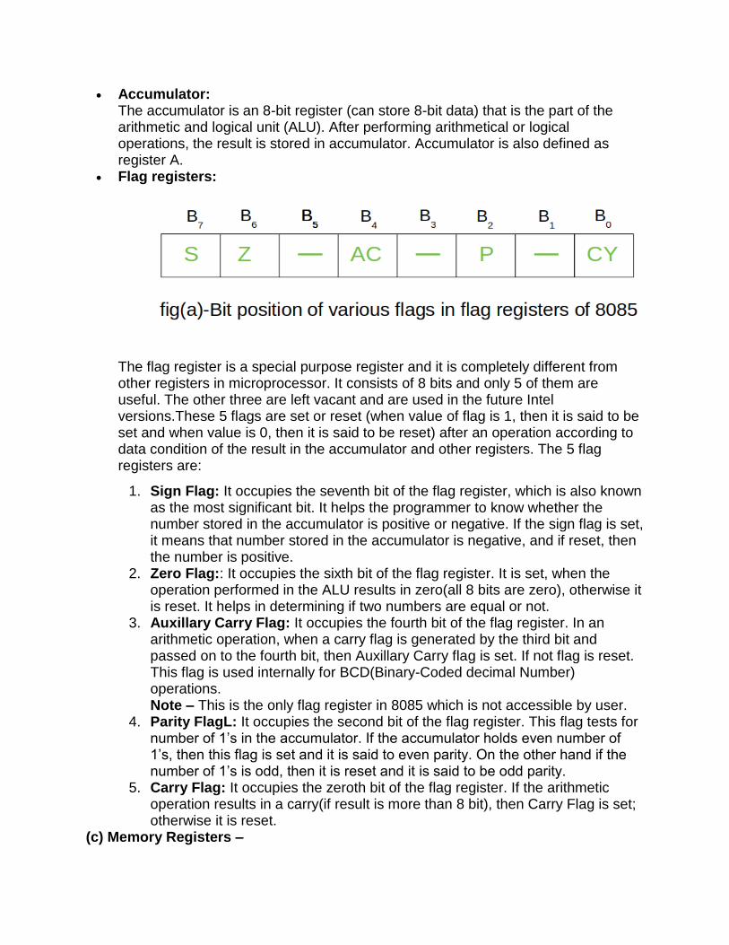
Flag registers:
The flag register is a special purpose register and it is completely different from other registers in microprocessor. It consists of 8 bits and only 5 of them are useful. The other three are left vacant and are used in the future Intel versions.These 5 flags are set or reset (when value of flag is 1, then it is said to be set and when value is 0, then it is said to be reset) after an operation according to data condition of the result in the accumulator and other registers. The 5 flag registers are:
1. Sign Flag: It occupies the seventh bit of the flag register, which is also known as the most significant bit. It helps the programmer to know whether the number stored in the accumulator is positive or negative. If the sign flag is set, it means that number stored in the accumulator is negative, and if reset, then the number is positive.
2. Zero Flag:: It occupies the sixth bit of the flag register. It is set, when the operation performed in the ALU results in zero(all 8 bits are zero), otherwise it is reset. It helps in determining if two numbers are equal or not.
3. Auxillary Carry Flag: It occupies the fourth bit of the flag register. In an arithmetic operation, when a carry flag is generated by the third bit and passed on to the fourth bit, then Auxillary Carry flag is set. If not flag is reset. This flag is used internally for BCD(Binary-Coded decimal Number) operations. Note – This is the only flag register in 8085 which is not accessible by user.
4. Parity FlagL: It occupies the second bit of the flag register. This flag tests for number of 1’s in the accumulator. If the accumulator holds even number of 1’s, then this flag is set and it is said to even parity. On the other hand if the number of 1’s is odd, then it is reset and it is said to be odd parity.
5. Carry Flag: It occupies the zeroth bit of the flag register. If the arithmetic operation results in a carry(if result is more than 8 bit), then Carry Flag is set; otherwise it is reset.
(c) Memory Registers –
There are two 16-bit registers used to hold memory addresses. The size of these registers is 16 bits because the memory addresses are 16 bits. They are :-
Program Counter: This register is used to sequence the execution of the instructions. The function of the program counter is to point to the memory address from which the next byte is to be fetched. When a byte (machine code) is being fetched, the program counter is incremented by one to point to the next memory location.
Stack Pointer: It is used as a memory pointer. It points to a memory location in read/write memory, called the stack. It is always incremented/decremented by 2 during push and pop operation.
Example – Here two binary numbers are added. The result produced is stored in the accumulator. Now lets check what each bit means. Refer to the below explanation simultaneously to connect them with the example.

Sign Flag (7th bit): It is reset(0), which means number stored in the accumulator is positive.
Zero Flag (6th bit): It is reset(0), thus result of the operations performed in the ALU is non-zero.
Auxiliary Carry Flag (4th bit): We can see that b3 generates a carry which is taken by b4, thus auxiliary carry flag gets set (1).
Parity Flag (2nd bit): It is reset(0), it means that parity is odd. The accumulator holds odd number of 1’s.
Carry Flag (0th bit): It is set(1), output results in more than 8 bit.
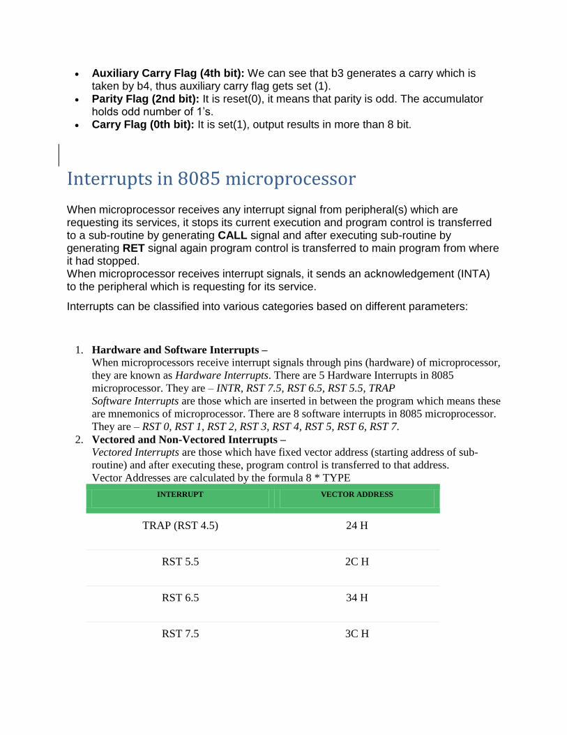
Interrupts in 8085 microprocessor
When microprocessor receives any interrupt signal from peripheral(s) which are requesting its services, it stops its current execution and program control is transferred to a sub-routine by generating CALL signal and after executing sub-routine by generating RET signal again program control is transferred to main program from where it had stopped. When microprocessor receives interrupt signals, it sends an acknowledgement (INTA) to the peripheral which is requesting for its service.
Interrupts can be classified into various categories based on different parameters:
1. Hardware and Software Interrupts – When microprocessors receive interrupt signals through pins (hardware) of microprocessor,
they are known as Hardware Interrupts. There are 5 Hardware Interrupts in 8085
microprocessor. They are – INTR, RST 7.5, RST 6.5, RST 5.5, TRAP
Software Interrupts are those which are inserted in between the program which means these
are mnemonics of microprocessor. There are 8 software interrupts in 8085 microprocessor.
They are – RST 0, RST 1, RST 2, RST 3, RST 4, RST 5, RST 6, RST 7.
2. Vectored and Non-Vectored Interrupts – Vectored Interrupts are those which have fixed vector address (starting address of sub-
routine) and after executing these, program control is transferred to that address.
Vector Addresses are calculated by the formula 8 * TYPE
INTERRUPT VECTOR ADDRESS
TRAP (RST 4.5) 24 H
RST 5.5 2C H
RST 6.5 34 H
RST 7.5 3C H

3. For Software interrupts vector addresses are given by:
INTERRUPT VECTOR ADDRESS
RST 0 00 H
RST 1 08 H
RST 2 10 H
RST 3 18 H
RST 4 20 H
RST 5 28 H
RST 6 30 H
RST 7 38 H
4. Non-Vectored Interrupts are those in which vector address is not predefined. The
interrupting device gives the address of sub-routine for these interrupts. INTR is the only
non-vectored interrupt in 8085 microprocessor.
5. Maskable and Non-Maskable Interrupts – Maskable Interrupts are those which can be disabled or ignored by the microprocessor.
These interrupts are either edge-triggered or level-triggered, so they can be disabled. INTR,
RST 7.5, RST 6.5, RST 5.5 are maskable interrupts in 8085 microprocessor.
Non-Maskable Interrupts are those which cannot be disabled or ignored by
microprocessor. TRAP is a non-maskable interrupt. It consists of both level as well as edge
triggering and is used in critical power failure conditions.
Priority of Interrupts – When microprocessor receives multiple interrupt requests simultaneously, it will execute the
interrupt service request (ISR) according to the priority of the interrupts.

Instruction for Interrupts –
1. Enable Interrupt (EI) – The interrupt enable flip-flop is set and all interrupts are enabled
following the execution of next instruction followed by EI. No flags are affected. After a
system reset, the interrupt enable flip-flop is reset, thus disabling the interrupts. This
instruction is necessary to enable the interrupts again (except TRAP).
2. Disable Interrupt (DI) – This instruction is used to reset the value of enable flip-flop
hence disabling all the interrupts. No flags are affected by this instruction.
Set Interrupt Mask (SIM) – It is used to implement the hardware interrupts (RST 7.5,
RST 6.5, RST 5.5) by setting various bits to form masks or generate output data via the
Serial Output Data (SOD) line. First the required value is loaded in accumulator then
SIM will take the bit pattern from it.

Read Interrupt Mask (RIM) – This instruction is used to read the status of the hardware interrupts (RST 7.5, RST 6.5, RST 5.5) by loading into the A register a byte which defines the condition of the mask bits for the interrupts. It also reads the condition of SID (Serial Input Data) bit on the microprocessor.
Addressing modes of 8085 in 8085 Microprocessor MicrocontrollerMicroprocessor8085
Using mnemonics without any alteration in the content, data can be transferred in three different cases –
From one register to another register
From the memory to the register and
From the register to the memory
These can be guided by addressing modes. Addressing modes in 8085 can be classified into 5 groups −
Immediate addressing mode
Register addressing mode
Direct addressing mode
Indirect addressing mode
Implied addressing mode
Immediate addressing mode

In this mode, the 8/16-bit data is specified in the instruction itself as one of its operands. For example MVI E, ABH means ABH is copied into register A.
MVI E ABH
Before After
(A) Any value ABH
As an example, if we consider instruction MVI E, ABH then it means that ABH will be moved or copied to the register E.And, as a result, the previous value of E will get overwritten.
Address Hex Codes
Mnemonic Comment
2000 1E MVI E, ABH E ← ABH
2001 AB
ABH as operand
This instruction will have seven T-states as shown below.
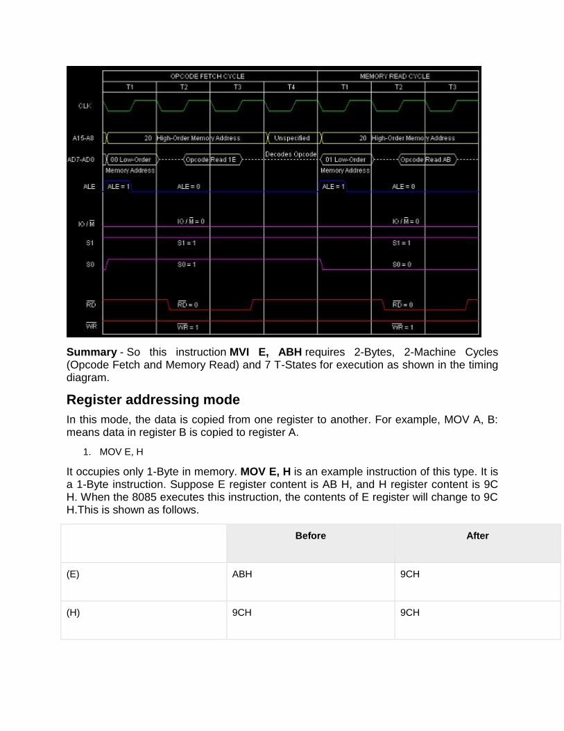
Summary - So this instruction MVI E, ABH requires 2-Bytes, 2-Machine Cycles (Opcode Fetch and Memory Read) and 7 T-States for execution as shown in the timing diagram.
Register addressing mode
In this mode, the data is copied from one register to another. For example, MOV A, B: means data in register B is copied to register A.
1. MOV E, H
It occupies only 1-Byte in memory. MOV E, H is an example instruction of this type. It is a 1-Byte instruction. Suppose E register content is AB H, and H register content is 9C H. When the 8085 executes this instruction, the contents of E register will change to 9C H.This is shown as follows.
Before After
(E) ABH 9CH
(H) 9CH 9CH
Address Hex Codes
Mnemonic Comment
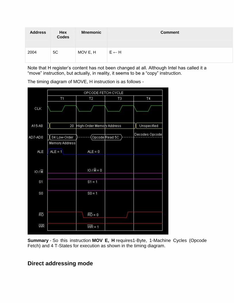
2004 5C MOV E, H E ← H
Note that H register’s content has not been changed at all. Although Intel has called it a “move” instruction, but actually, in reality, it seems to be a “copy” instruction.
The timing diagram of MOVE, H instruction is as follows -
Summary - So this instruction MOV E, H requires1-Byte, 1-Machine Cycles (Opcode Fetch) and 4 T-States for execution as shown in the timing diagram.
Direct addressing mode

In this mode, the data is directly copied from the given address to the register. For example LDA 3000H: means the data at address 3000H is copied to register A.
1. LDA 4050H
Let us consider LDA 4050 Has an example instruction of this type. It is a 3-Byte instruction. The initial content of memory address 4050H is ABH. initial accumulator content is CDH. As after execution A will be initialized with value ABH. Memory location 4050H will still remain with the content ABH. The results of the execution of this instruction are as below –
Before After
(4050) ABH ABH
A CDH ABH
Address Hex
Codes
Mnemonic Comment
2008 3A LDA 4050H A ← Content of the memory location 4050H
2009 50
Low order Byte of the address
200A 40 High order Byte of the address
Here is the timing diagram of the instruction LDA 4050H –

Summary - So this instruction LDA 4050H requires 3-Bytes, 4-Machine Cycles (Opcode Fetch, Memory Read, Memory Read, Memory Read) and 13 T-States for execution as shown in the timing diagram.
Indirect addressing mode
In this mode, the data is transferred from one register to another by using the address pointed by the register. For example, MOV A, M: means data is transferred from the memory address pointed by the register pair HL to the register A.
1. MOV E, M
It occupies only 1-Byte in memory. MOVE, M is an example instruction of this type. It is a 1-Byte instruction. Suppose E register content is DBH, H register content is 40H, and L register content is 50H. Letus say location 4050H has the data value AAH. When the 8085 executes this instruction, the contents of E register will change to AAH, as shown below –
Before After
(E) DBH AAH
(HL) 4050H 4050H
(4050H) AAH AAH

Address Hex Codes Mnemonic Comment
2008 2A MOV E, M E ← Content of the memory location pointed by HL register pair
The timing diagram for this MOV E, M instruction is as follows –
Summary - So this instruction MOV E, M requires 1-Byte, 2-Machine Cycles (Opcode Fetch, Memory Read) and 7 T-States for execution as shown in the timing diagram.
Implied addressing mode
This mode doesn’t require any operand; the data is specified by the opcode itself. For example: CMA, CMP.
1. CMP E
Let us consider one sample instruction CMPE falling in this category. It is a 1-Byte instruction so during execution of this instruction it will occupy only a single Byte in memory. The result of the execution of this instruction has been depicted with the following set of examples –
Example 1
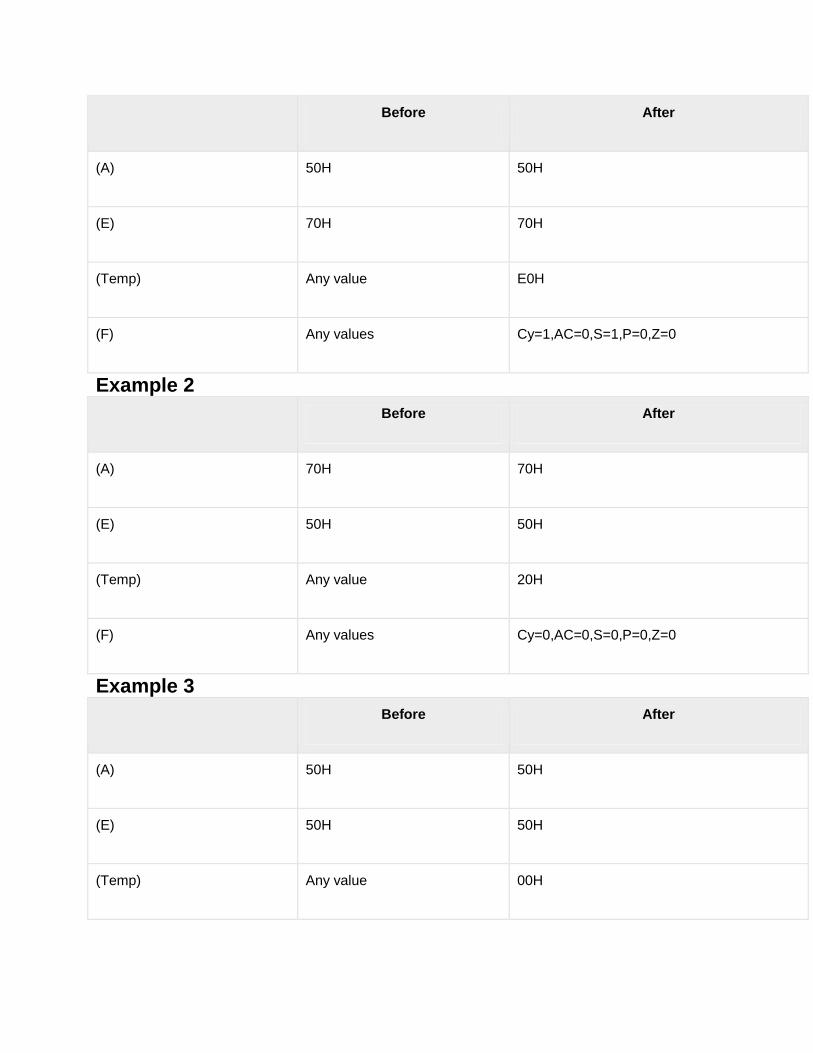
Before After
(A) 50H 50H
(E) 70H 70H
(Temp) Any value E0H
(F) Any values Cy=1,AC=0,S=1,P=0,Z=0
Example 2
Before After
(A) 70H 70H
(E) 50H 50H
(Temp) Any value 20H
(F) Any values Cy=0,AC=0,S=0,P=0,Z=0
Example 3
Before After
(A) 50H 50H
(E) 50H 50H
(Temp) Any value 00H

Before After
(F) Any values Cy=0,AC=0,S=0,P=1,Z=1
Address Hex
Codes
Mnemonic Comment
2004 BB CMP E Temp = Register A - Register E
The timing diagram against this instruction CMP Execution is as follows –
