adc test setup - university of california, berkeleyee247/fa05/lectures/l15_all_f05.pdf · • not...
TRANSCRIPT
EECS 247 Lecture 15: Data Converters © 2005 H.K. Page 1
EE247Lecture 15
Data Converters• Practical aspects of converter testing
• Signal source• Filters for signal source harmonic distortion
attenuation• Clock generator requirements• Evaluation board considerations
• D/A converter design
EECS 247 Lecture 15: Data Converters © 2005 H.K. Page 2
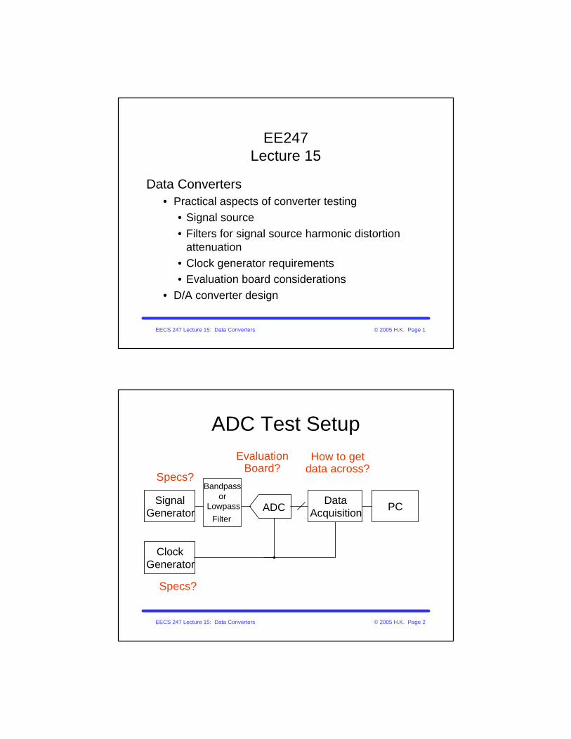
ADC Test SetupEvaluation
Board?How to get
data across?Specs?
Specs?
Vin PCSignalGenerator
ClockGenerator
DataAcquisitionADC
Bandpass or
Lowpass
Filter

EECS 247 Lecture 15: Data Converters © 2005 H.K. Page 3
Clock Generator• Let us check if for the clock a "value-
priced" signal generator will suffice...• No! The clock signal controls sampling
instants – which we assumed to be precisely equi-distant in time (period T)
• Variability in T causes errors– "Aperture Uncertainty" or "Aperture Jitter"
• How much Jitter can we tolerate?
EECS 247 Lecture 15: Data Converters © 2005 H.K. Page 4
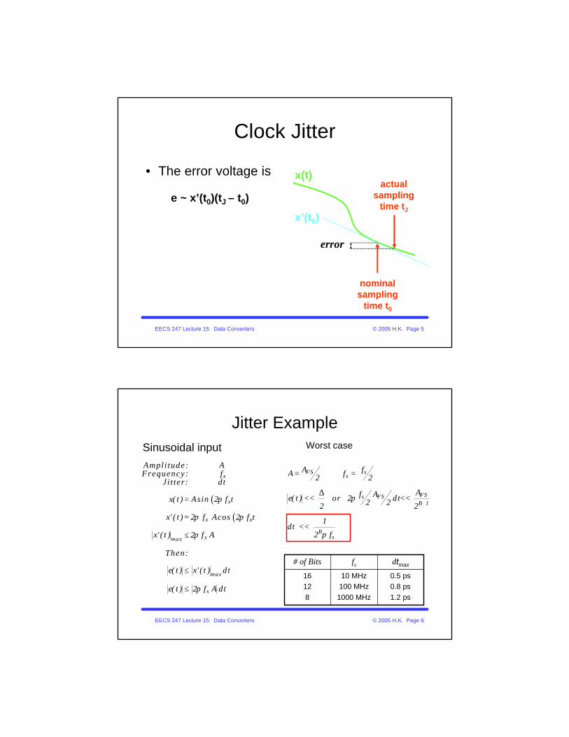
Clock Jitter
• Sampling jitter adds an error voltage proportional to the product of (tJ-t0) and the derivative of the input signal at the sampling instant
• Jitter doesn’t matter when sampling dc signals (x’ (t0 )=0)
nominal (ideal) sampling
time t0
actualsampling
time tJ
x(t)
x’(t0)
Instantaneous
jitter
EECS 247 Lecture 15: Data Converters © 2005 H.K. Page 5
Clock Jitter
• The error voltage is
nominalsampling
time t0
actualsampling
time tJ
x(t)
x’(t0)
e ~ x’(t0)(tJ – t0)
error
EECS 247 Lecture 15: Data Converters © 2005 H.K. Page 6
Jitter ExampleSinusoidal input Worst case
0.5 ps0.8 ps1.2 ps
10 MHz100 MHz
1000 MHz
16128
dtmaxfs# of Bits
( )
( )
x
x
x x
xmax
max
x
Ampli tude: AFrequency: f
J i t ter: dt
x( t ) Asin 2 f t
x' ( t ) 2 f Acos 2 f t
x' ( t ) 2 f A
Then:
e( t ) x' ( t ) dt
e( t ) 2 f A dt
π
π π
π
π
=
=
≤
≤
≤
sFSx
FSs FSB 1
Bs
fAA f2 2
Af Ae( t ) or 2 dt2 22 2
1dt
2 f
π
π
+
= =
∆<< <<
<<

EECS 247 Lecture 15: Data Converters © 2005 H.K. Page 7
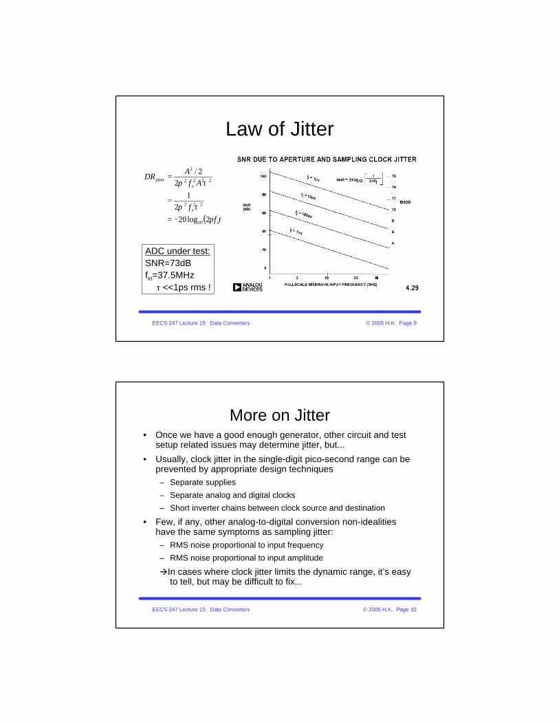
Law of Jitter
• The worst case looks pretty stringent …what about less conservative statistical “average”?
• Let’s calculate the mean squared jitter error (variance)• Assume sampling a sinusoidal signal
x(t) = Asin(2πfxt), then– x’(t) = 2πfxAcos(2πfxt)– E[x’(t)]2 = 2π2fx2A2
• Assume the jitter has variance E(tJ-t0)2 = τ2
EECS 247 Lecture 15: Data Converters © 2005 H.K. Page 8
Law of Jitter
• If x’(t) and the jitter are independent
– E[x’(t)(tJ-t0)]2= E[x’(t)]2 E(tJ-t0)2
• Hence, the jitter error power is
Ee2 = 2π2fx2A2τ2
EECS 247 Lecture 15: Data Converters © 2005 H.K. Page 9
Law of Jitter
( )τπτπ
τπ
x
x
x
ff
AfA
DR
2log202
12
2/
10
222
2222
2
jitter
−=
=
=
ADC under test:SNR=73dBfin=37.5MHz⇒ τ <<1ps rms !
EECS 247 Lecture 15: Data Converters © 2005 H.K. Page 10
More on Jitter• Once we have a good enough generator, other circuit and test
setup related issues may determine jitter, but...
• Usually, clock jitter in the single-digit pico-second range can be prevented by appropriate design techniques– Separate supplies
– Separate analog and digital clocks
– Short inverter chains between clock source and destination
• Few, if any, other analog-to-digital conversion non-idealities have the same symptoms as sampling jitter:– RMS noise proportional to input frequency
– RMS noise proportional to input amplitude
àIn cases where clock jitter limits the dynamic range, it’s easy to tell, but may be difficult to fix...

EECS 247 Lecture 15: Data Converters © 2005 H.K. Page 11
Evaluation Board
• Planning begins with converter pin-out– Example of poor pin-outà clock pin right next to a digital
output...
• Not "Black Magic", but weeks of design time and studying
• Key aspects– Supply/ground routing, bypass capacitors– Coupling between signals
• Good idea to look at ADC vendor datasheets for example layouts/schematics/application notes
EECS 247 Lecture 15: Data Converters © 2005 H.K. Page 12
Vendor Eval Board Layout
[Analog Devices AD9235 Data Sheet]

EECS 247 Lecture 15: Data Converters © 2005 H.K. Page 13
One thing to remember...• A converter does not just have one "input" pin
but:– Clock– Power Supply, Ground– Reference Voltage
• For good practices on how to avoid issues see e.g.:– Analog Devices Application Note 345: "Grounding
for Low-and-High-Frequency Circuits"– Maxim Application Note 729: "Dynamic Testing of
High-Speed ADCs, Part 2"
EECS 247 Lecture 15: Data Converters © 2005 H.K. Page 14
How to Get the Bits Off Chip?
• "Full swing" CMOS signaling works well forfCLK<100MHz- For higher frequencies:– Uncontrolled characteristic impedance– High swingà higher level of spurious coupling to other
signals– Low power efficiency
• But we want to build faster ADCs...• Alternative to CMOS: LVDS – Low Voltage
Differential Signaling• LVDS vs. CMOS:
– Higher speed, more power efficient at high speed– Two pins/bit!

EECS 247 Lecture 15: Data Converters © 2005 H.K. Page 15
LVDS Outputs
Analog Devices Application Note 586: "LVDS Data Outputs for High Speed ADCs"
EECS 247 Lecture 15: Data Converters © 2005 H.K. Page 16
LVDS Outputs
Analog Devices Application Note 586: "LVDS Data Outputs for High Speed ADCs"
EECS 247 Lecture 15: Data Converters © 2005 H.K. Page 17
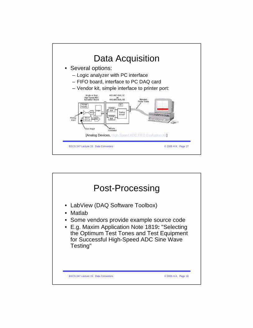
Data Acquisition• Several options:
– Logic analyzer with PC interface– FIFO board, interface to PC DAQ card– Vendor kit, simple interface to printer port:
[Analog Devices, High-Speed ADC FIFO Evaluation Kit]
EECS 247 Lecture 15: Data Converters © 2005 H.K. Page 18
Post-Processing
• LabView (DAQ Software Toolbox)• Matlab• Some vendors provide example source code• E.g. Maxim Application Note 1819: "Selecting
the Optimum Test Tones and Test Equipment for Successful High-Speed ADC Sine Wave Testing"
EECS 247 Lecture 15: Data Converters © 2005 H.K. Page 19
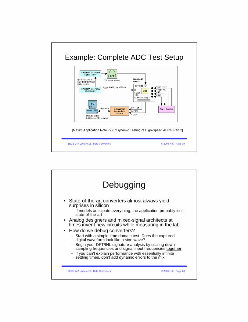
Example: Complete ADC Test Setup
[Maxim Application Note 729: "Dynamic Testing of High-Speed ADCs, Part 2]
EECS 247 Lecture 15: Data Converters © 2005 H.K. Page 20
Debugging
• State-of-the-art converters almost always yield surprises in silicon– If models anticipate everything, the application probably isn’t
state-of-the-art• Analog designers and mixed-signal architects at
times invent new circuits while measuring in the lab• How do we debug converters?
– Start with a simple time domain test. Does the captured digital waveform look like a sine wave?
– Begin your DFT/INL signature analysis by scaling down sampling frequencies and signal input frequencies together
– If you can’t explain performance with essentially infinite settling times, don’t add dynamic errors to the mix

EECS 247 Lecture 15: Data Converters © 2005 H.K. Page 21
Debugging
• Typical problems come from non-idealities never built into your "model"– E.g. half-circuit models for fully-differential
circuits inherently can’t explain some types of differential-symmetry errors
• You can’t afford to rediscover old non-idealities in new silicon– Talking to veterans early in the modeling
phase can be important
EECS 247 Lecture 15: Data Converters © 2005 H.K. Page 22
Debugging• Design teams usually track down and fix single-cause
problems quickly• Problems due to circuit interactions are much more
difficult to debug, try to avoid by good design/layout• Interaction examples:
– Digital activity-dependent clock jitter• S/(N+D) degradation only happens when large
amplitude, high frequency analog inputs coincide with the offending digital activity
– Distortion cancellation• Nonlinear phenomena don’t obey superposition
EECS 247 Lecture 15: Data Converters © 2005 H.K. Page 23
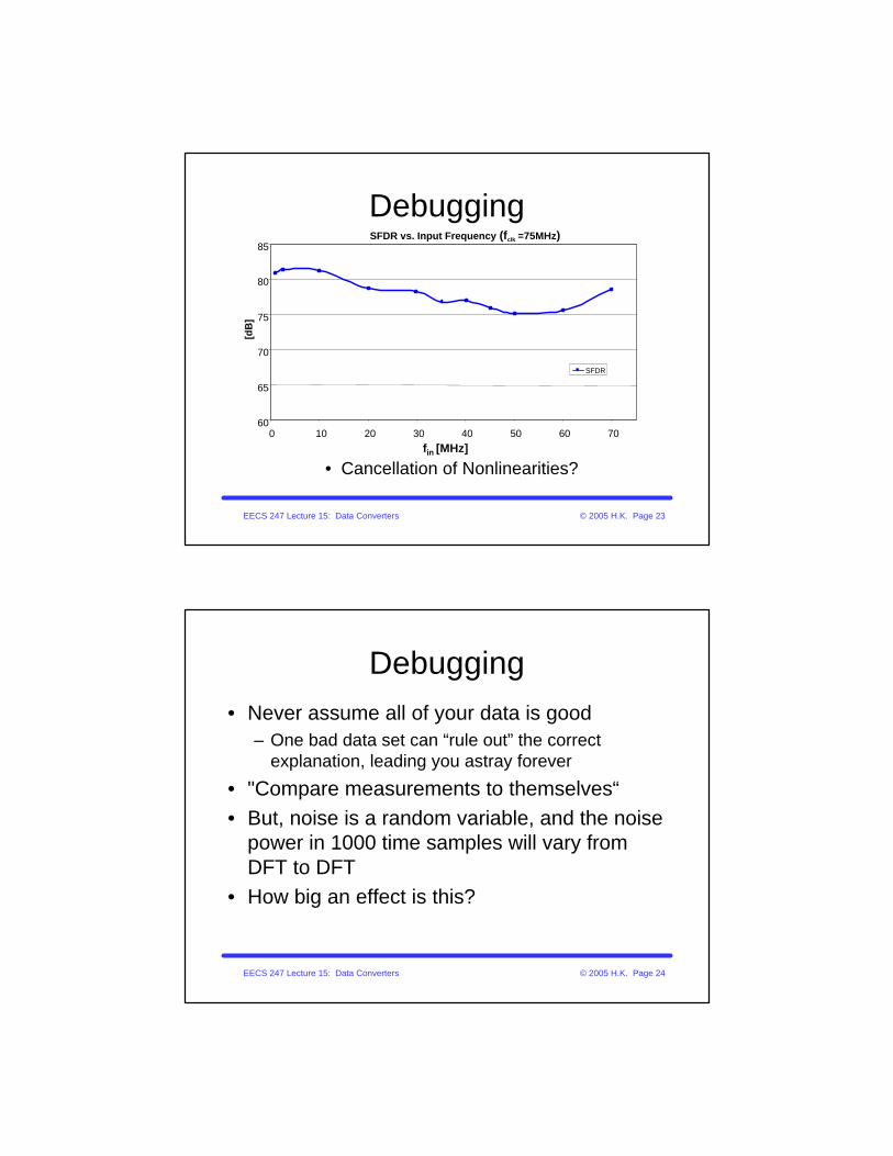
Debugging
• Cancellation of Nonlinearities?
SFDR vs. Input Frequency (fclk =75MHz)
60
65
70
75
80
85
0 10 20 30 40 50 60 70fin [MHz]
[dB
]
SFDR
EECS 247 Lecture 15: Data Converters © 2005 H.K. Page 24
Debugging• Never assume all of your data is good
– One bad data set can “rule out” the correct explanation, leading you astray forever
• "Compare measurements to themselves“• But, noise is a random variable, and the noise
power in 1000 time samples will vary from DFT to DFT
• How big an effect is this?
EECS 247 Lecture 15: Data Converters © 2005 H.K. Page 25
Debugging
• Can show that:– Variation of noise in 1000 samples yields a
standard deviation in SNR of 0.2dB– This means that 68.3% of all DFTs will produce
SNRs within 0.2dB of the average– 99.7% of 1000 point DFTs yield SNRs within
±0.6dB of the average
• If you’re seeing ADC noise variation of greater than ±0.6dB in the lab, some sort of interference is usually the culprit
EECS 247 Lecture 15: Data Converters © 2005 H.K. Page 26
Testing & Debugging
• Always try to use two independent measurement methods to verify important results– Correlate INL & SFDR, DNL & SNR
• Comparing time domain and frequency domain views of the same measurement is good practice– e.g. DNL & SNR
Debugging and testing of state-of-the-art circuitryà Non-trivialà Need to plan ahead
EECS 247 Lecture 15: Data Converters © 2005 H.K. Page 27
D/A Converters• D/A architecture examples
– Unit element– Binary weighted
• Static performance– Component matching– Architectures
• Unit element• Binary weighted• Segmented
– Dynamic element matching
• Dynamic performance– Glitches
• DAC examples
EECS 247 Lecture 15: Data Converters © 2005 H.K. Page 28
D/A Converters
• Comprises voltage, charge, or current based elements
• Examples for above three categories:– Resistor string– Charge redistribution– Current source type
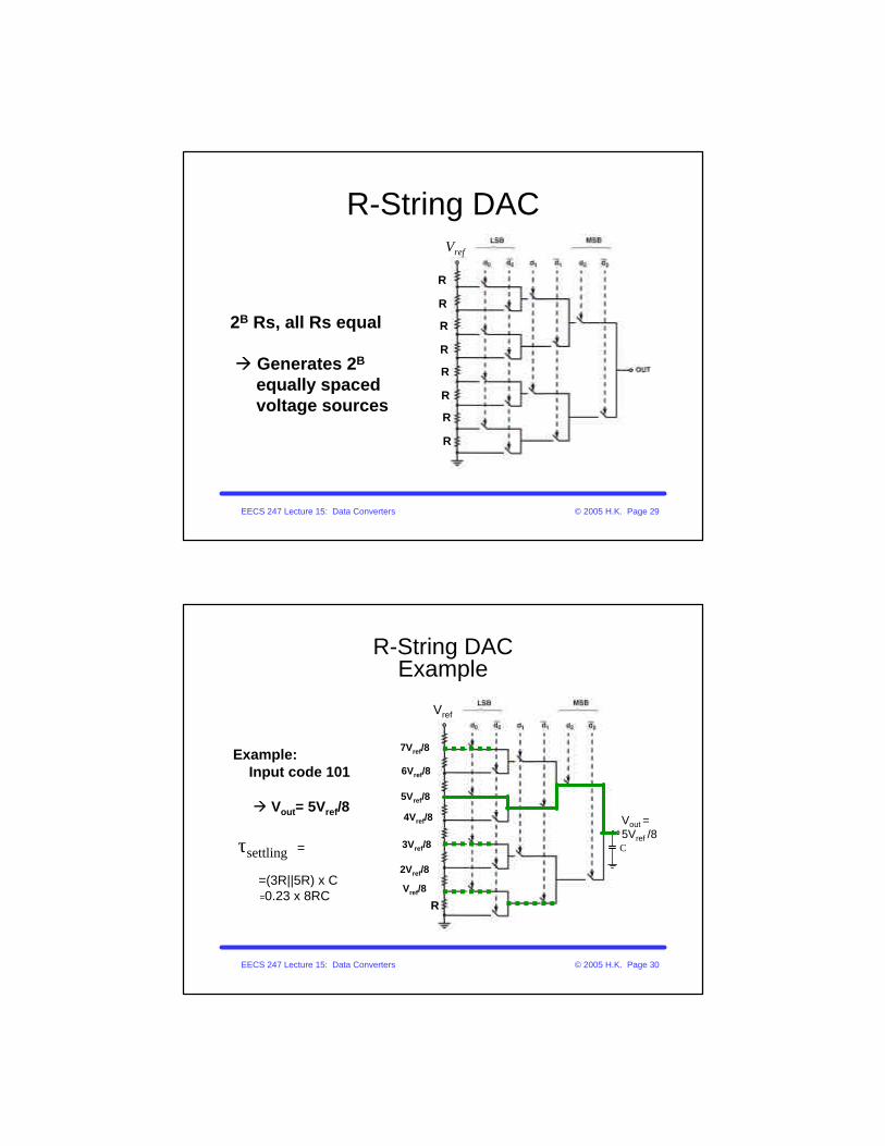
EECS 247 Lecture 15: Data Converters © 2005 H.K. Page 29
R-String DAC
R
R
R
R
R
R
R
R
2B Rs, all Rs equal
à Generates 2B
equally spaced voltage sources
Vref
EECS 247 Lecture 15: Data Converters © 2005 H.K. Page 30
R-String DACExample
Example: Input code 101
à Vout= 5Vref/8
τsettling =
=(3R||5R) x C=0.23 x 8RC
Vref/8
2Vref/8
3Vref/8
4Vref/8
5Vref/8
6Vref/8
7Vref/8
C
R
Vref
Vout = 5Vref /8

EECS 247 Lecture 15: Data Converters © 2005 H.K. Page 31
R-String DAC
• Advantages:– Simple, fast for <8-10bits– Inherently monotonic– Compatible with purely digital
technologies
• Disadvantages:– 2B resistors & ~22B switches for
B bits à High element count & large area for B >10bits
– High settling time for B > 10:τmax = 0.25 x 2B RC
C
Ref:M. Pelgrom, “A 10-b 50-MHz CMOS D/A Converter with 75-W Buffer,” JSSC, Dec. 1990, pp. 1347
Vref
EECS 247 Lecture 15: Data Converters © 2005 H.K. Page 32
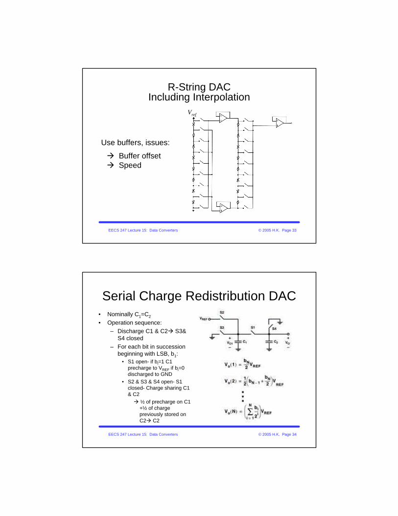
R-String DACIncluding Interpolation
Resistor string DAC+ Resistor string interpolator increases resolution w/o drastic increase in complexitye.g. 6bit DACà 3bit +3bit
Considerations:q Interpolation string loading of main
R-stringq Large R values à less loading but
lower speedq Can use buffers
Vout
Vref
EECS 247 Lecture 15: Data Converters © 2005 H.K. Page 33
R-String DACIncluding Interpolation
Use buffers, issues:
à Buffer offset à Speed
Vref
EECS 247 Lecture 15: Data Converters © 2005 H.K. Page 34
Serial Charge Redistribution DAC• Nominally C1=C2
• Operation sequence:– Discharge C1 & C2à S3&
S4 closed– For each bit in succession
beginning with LSB, b1:• S1 open- if bi=1 C1
precharge to VREF if bi=0 discharged to GND
• S2 & S3 & S4 open- S1 closed- Charge sharing C1 & C2à ½ of precharge on C1
+½ of charge previously stored on C2à C2
EECS 247 Lecture 15: Data Converters © 2005 H.K. Page 35
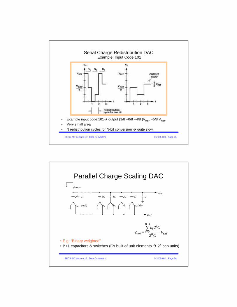
Serial Charge Redistribution DACExample: Input Code 101
• Example input code 101à output (1/8 +0/8 +4/8 )VREF =5/8 VREF
• Very small area• N redistribution cycles for N-bit conversion à quite slow
b1 b2 b3
EECS 247 Lecture 15: Data Converters © 2005 H.K. Page 36
Parallel Charge Scaling DAC
• E.g. “Binary weighted”• B+1 capacitors & switches (Cs built of unit elements à 2B cap units)
CC2C4C8C2(B-1) C
Vref
Vout
reset
b0 (lsb)b1b2b3bB-1 (msb)
B 1i
ii 0out refB
b 2 CV V
2 C
−
==∑
EECS 247 Lecture 15: Data Converters © 2005 H.K. Page 37
Charge Scaling DACExample: 4Bit DAC- Input Code 1011
CC2C4C8C
Vref
Vout
b0 (lsb)b1
b2b3
CC2C4C8C
Vref
Voutreset
b0 (lsb)b1b2b3
b- Charge phasea- Reset phase
0 1 3out ref ref4
2 C 2 C 2 C 11V V V2 C 16
=+ +=
EECS 247 Lecture 15: Data Converters © 2005 H.K. Page 38
Charge Scaling DAC
• Monotonicity depends on element matching• Sensitive to parasitic capacitor @ outputà gain error• Large area of caps for high DAC resolution (10bit DAC ratio 1:512)
refP
B
B
i
ii
out VCC
CbV
+=
∑−
=
2
21
0
CC2C4C8C2(B-1) C
Vref
Vout
reset
b0 (lsb)b1b2b3bB-1 (msb)
CP

EECS 247 Lecture 15: Data Converters © 2005 H.K. Page 39
Charge Scaling DAC
• Opamp helps eliminate the parasitic capacitor effect– Issue: opamp offset & speed
C2C4C8C2(B-1) C
Vref
Vout
reset
b0 (lsb)b1b2b3bB-1 (msb)
CP
CI
-
+
CI
B 1i
ii 0
out refI
b 2 CV V
C
−
==∑
EECS 247 Lecture 15: Data Converters © 2005 H.K. Page 40
Charge Scaling DACUtilizing Split Array
• Split arrayà reduce the total area of the capacitors required– E.g. 10bit regular binary array requires 513 unit Cs while split array (5&5)
needs 64 unit Cs– Issue: Sensitive to parasitic C
C 2C 4C
Vref
Vout
reset
b5b4b3b2
+
-
series
al l LSB array CC C
all MSB array C=
∑
∑
8/7C
C 2C 4C
b1b0
C

EECS 247 Lecture 15: Data Converters © 2005 H.K. Page 41
Resistor Ladder (MSB) & Binary Weighted Charge Scaling (LSB) Segmented DAC
CC2C4C8C32 C
reset
b1b2b3b5
16C
b4
Vout
b0
..........
SwitchNetwork
6bitresistorladder
6-bitbinary weighted charge redistribution DAC
• Example: 12bit DAC
– 6-bit MSB DACà R string
– 6-bit LSB DAC à binary weighted charge redistribution
• Complexity much lower than full R
string
– Full R stringà4096 resistors
– Segmented à64 R + 7 Cs (64 unit caps)
EECS 247 Lecture 15: Data Converters © 2005 H.K. Page 42
Current Source DACUnit Element
• “Unit elements ”• Monotonicity does not depend on element matching• 2B-1 current sources & switches • Suited for both MOS and BJT techologies• Output resistance of current source à gain error
Iref Iref
Iout
IrefIref
……………
……………

EECS 247 Lecture 15: Data Converters © 2005 H.K. Page 43
Current Source DACUnit Element
• Output resistance of current source à gain error problemà Use transresistance amplifier- output of current source held
@ virtual ground – error due to current source output resistance elliminated
Iref IrefIrefIref
……………
……………
Vout
R
-
+
EECS 247 Lecture 15: Data Converters © 2005 H.K. Page 44
Current Source DACBinary Weighted
• “Binary weighted”• Monotonicity depends on element matching• B current sources & switches (2B-1 unit elements)
4 Iref Iref
Iout
2Iref2B-1 Iref
……………
……………
EECS 247 Lecture 15: Data Converters © 2005 H.K. Page 45
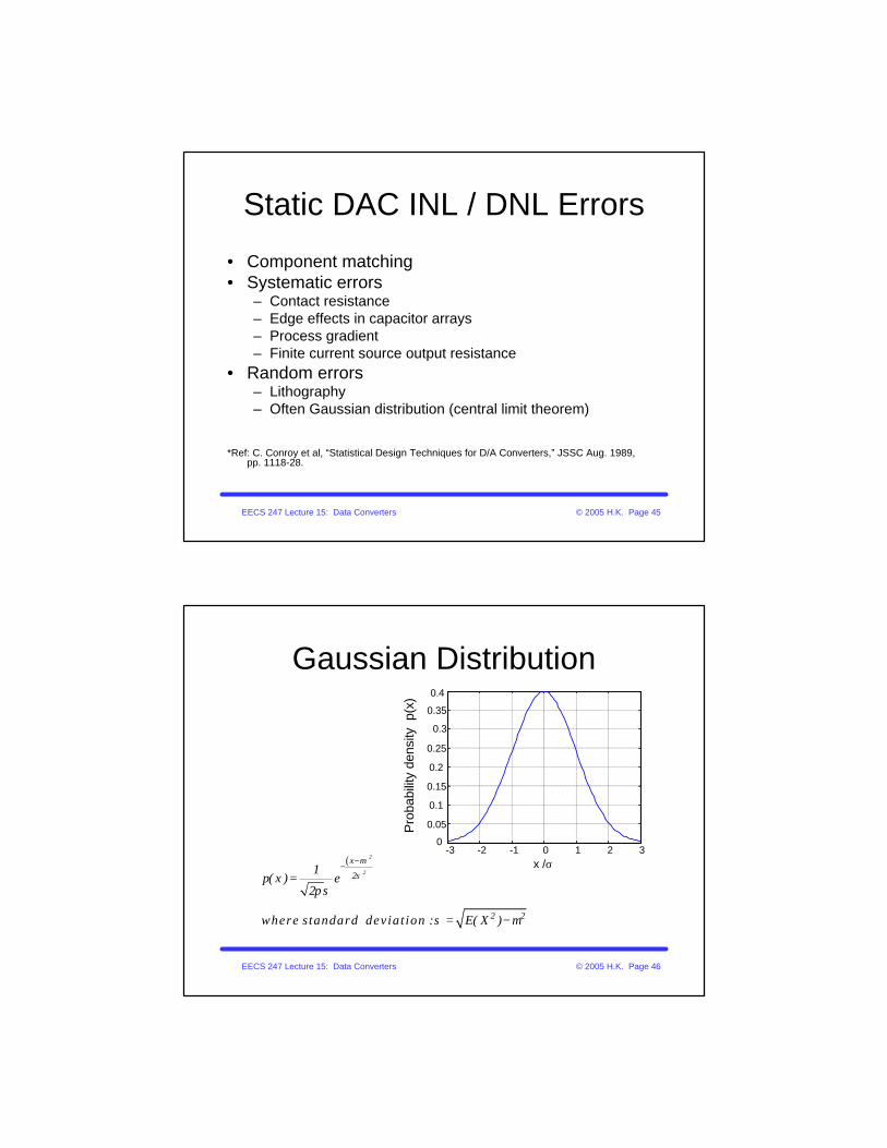
Static DAC INL / DNL Errors
• Component matching• Systematic errors
– Contact resistance– Edge effects in capacitor arrays– Process gradient– Finite current source output resistance
• Random errors– Lithography– Often Gaussian distribution (central limit theorem)
*Ref: C. Conroy et al, “Statistical Design Techniques for D/A Converters,” JSSC Aug. 1989, pp. 1118-28.
EECS 247 Lecture 15: Data Converters © 2005 H.K. Page 46
Gaussian Distribution
-3 -2 -1 0 1 2 30
0.05
0.1
0.15
0.2
0.25
0.3
0.35
0.4
x /σ
Pro
babi
lity
dens
ity p
(x)
( )2
2
x
2
2 2
1p( x ) e
2
where standard deviat ion : E( X )
µ
σ
πσ
σ µ
−−
=
= −
EECS 247 Lecture 15: Data Converters © 2005 H.K. Page 47
Yield
( )2xX
2
X
P X x X
1e dx
2
Xerf
2
π
+ −
−
− ≤ ≤ + =
=
=
∫ 0
0.1
0.2
0.3
0.4
Pro
babi
lity
dens
ity
p(x)
0 0.5 1 1.5 2 2.5 30
0.20.40.60.8
1
X
38.3
68.3
95.4
P(-
X ≤
x ≤
+X
)
EECS 247 Lecture 15: Data Converters © 2005 H.K. Page 48
Yield
X/σ P(-X ≤ x ≤ X) [%]
0.2000 15.85190.4000 31.08430.6000 45.14940.8000 57.62891.0000 68.26891.2000 76.98611.4000 83.84871.6000 89.04011.8000 92.81392.0000 95.4500
X/σ P(-X ≤ x ≤ X) [%]
2.2000 97.21932.4000 98.36052.6000 99.06782.8000 99.48903.0000 99.73003.2000 99.86263.4000 99.93263.6000 99.96823.8000 99.98554.0000 99.9937

EECS 247 Lecture 15: Data Converters © 2005 H.K. Page 49
Example
• Measurements show that the offset voltage of a batch of operational amplifiers follows a Gaussian distribution with σ = 2mV and µ = 0.
• Fraction of opamps with |Vos| < X = 6mV:– X/σ = 3 à 99.73 % yield (we’d still test before
shipping!)
• Fraction of opamps with |Vos| < X = 400µV:– X/σ = 0.2 à 15.85 % yield
EECS 247 Lecture 15: Data Converters © 2005 H.K. Page 50
Component Mismatch
R
R
∆
10000
100
200
300
400
No.
of r
esis
tors
1004 1008 1012996992988R[ ]Ω
Example: Two side-by-sideResistors
E.g. Let us assume in this example 1000 Rs measured & 68.5% within +-4OHM or +-0.4% of averageà 1σ for resistorsà 0.4%
Large # of devices measured & curved à typically if sample size large shape is Gaussian

EECS 247 Lecture 15: Data Converters © 2005 H.K. Page 51
Component Mismatch
1 2
1 2
2dR
R
R RR
2
dR R R
1
Areaσ
+=
= −
∝
R
R
∆
00
0.05
0.1
0.15
0.2
0.25
0.3
0.35
0.4
Pro
babi
lity
dens
ity p
(x)
σ 2σ 3σ−σ−2σ−3σdR
R
Two side-by-sideResistors
For typical technologies & geometries1σ for resistorsà 0.02 το 5%
In the case of resistors σ is a function of area
EECS 247 Lecture 15: Data Converters © 2005 H.K. Page 52
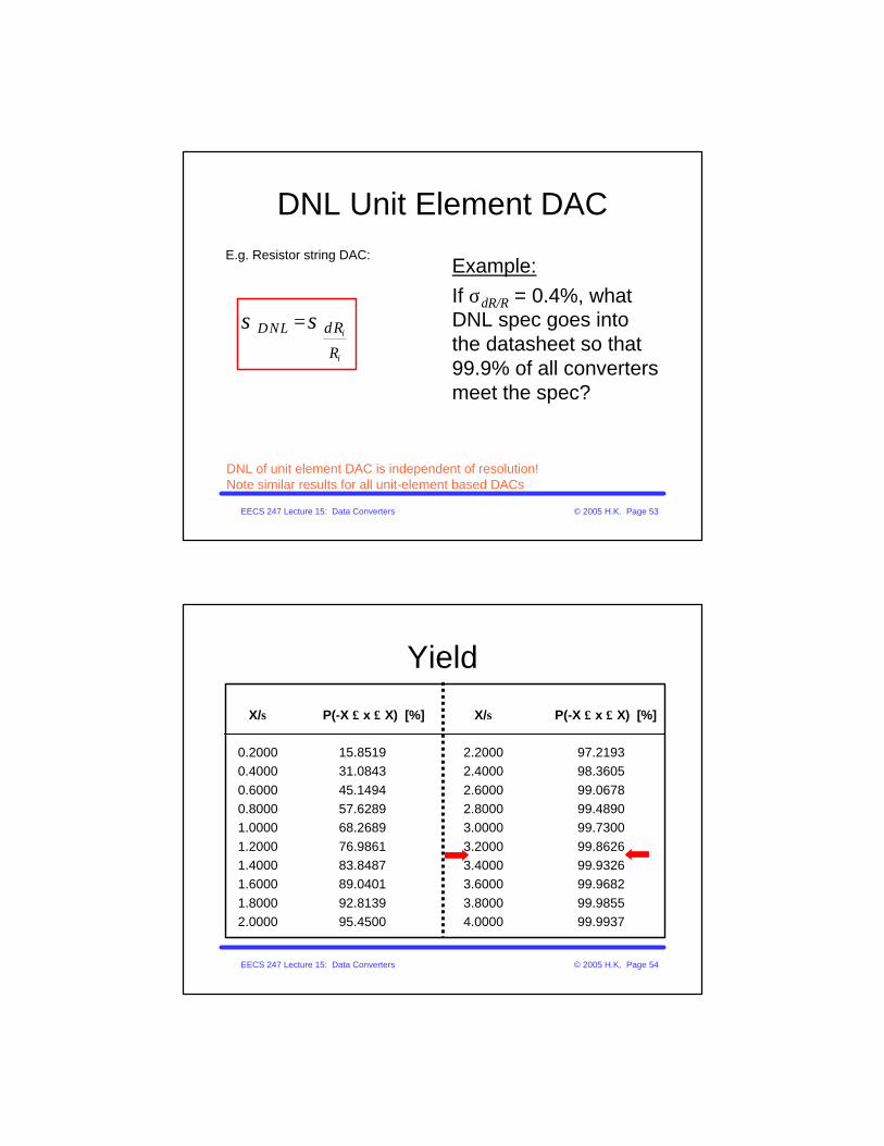
DNL Unit Element DAC
i i refR I∆ =
DNL of unit element DAC is independent of resolution!
E.g. Resistor string DAC:
Iref
i
i
nom ref
i i ref
nom ii
nom
i nom nom nom
nom nom i
DNL dR
R
R I
R I
DNL
R R dR dR
R R R
σ σ
∆ =
∆ =
∆ − ∆=
∆
−= = ≈
=
Vref
EECS 247 Lecture 15: Data Converters © 2005 H.K. Page 53
DNL Unit Element DAC
Example:If σdR/R = 0.4%, what DNL spec goes into the datasheet so that 99.9% of all converters meet the spec?
DNL of unit element DAC is independent of resolution!Note similar results for all unit-element based DACs
E.g. Resistor string DAC:
i
i
DNL dR
R
σ σ=
EECS 247 Lecture 15: Data Converters © 2005 H.K. Page 54
Yield
X/σ P(-X ≤ x ≤ X) [%]
0.2000 15.85190.4000 31.08430.6000 45.14940.8000 57.62891.0000 68.26891.2000 76.98611.4000 83.84871.6000 89.04011.8000 92.81392.0000 95.4500
X/σ P(-X ≤ x ≤ X) [%]
2.2000 97.21932.4000 98.36052.6000 99.06782.8000 99.48903.0000 99.73003.2000 99.86263.4000 99.93263.6000 99.96823.8000 99.98554.0000 99.9937
EECS 247 Lecture 15: Data Converters © 2005 H.K. Page 55
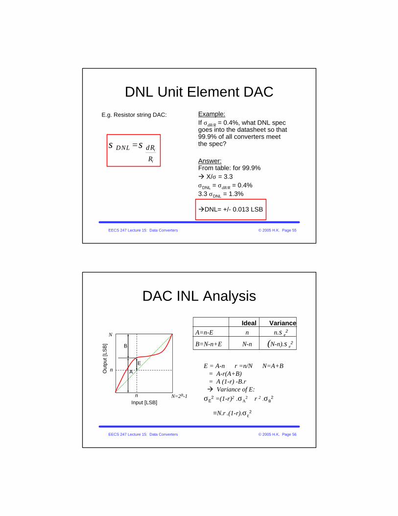
DNL Unit Element DACExample:If σdR/R = 0.4%, what DNL spec goes into the datasheet so that 99.9% of all converters meet the spec?
Answer:From table: for 99.9% à X/σ = 3.3σDNL = σdR/R = 0.4%3.3 σDNL = 1.3%
àDNL= +/- 0.013 LSB
E.g. Resistor string DAC:
i
i
DNL dR
R
σ σ=
EECS 247 Lecture 15: Data Converters © 2005 H.K. Page 56
DAC INL Analysis
B
A
N=2B-1n
n
N
Out
put [
LSB
]
Input [LSB]
E
Ideal VarianceA=n-E n n.σε
2
B=N-n+E N-n (N-n).σε2
E = A-n r =n/N N=A+B= A-r(A+B)= A (1-r) -B.rà Variance of E:
σE2 =(1-r)2 .σΑ
2 + r 2 .σB2
=N.r .(1-r).σε2
EECS 247 Lecture 15: Data Converters © 2005 H.K. Page 57
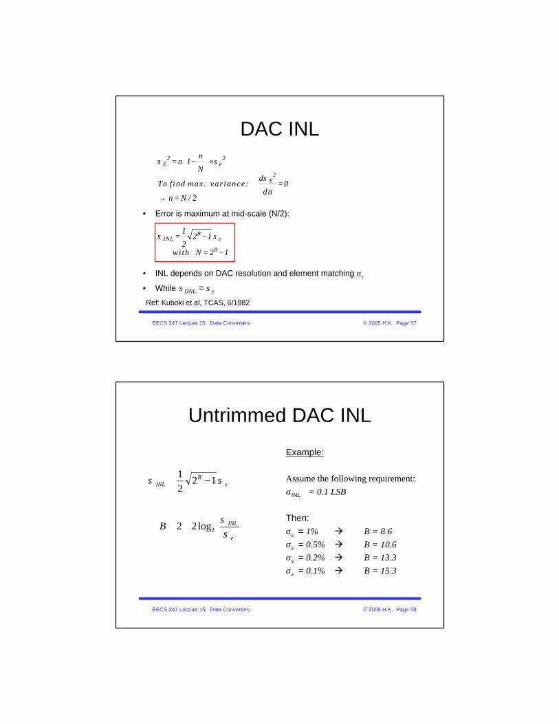
DAC INL
• Error is maximum at mid-scale (N/2):
• INL depends on DAC resolution and element matching σε
• While σDNL = σε
Ref: Kuboki et al, TCAS, 6/1982
2 2E
2E
BINL
B
n1n
Nd
To find max. variance: 0dn
n N / 2
12 1
2 with N 2 1
ε
ε
σ σ
σ
σ σ
−= ×
=
→ =
= −
= −
EECS 247 Lecture 15: Data Converters © 2005 H.K. Page 58
Untrimmed DAC INL
Example:
Assume the following requirement:σINL = 0.1 LSB
Then:σε = 1% à B = 8.6σε = 0.5% à B = 10.6σε = 0.2% à B = 13.3σε = 0.1% à B = 15.3
+≅
−≅
ε
ε
σσ
σσ
INL
BINL
B 2log22
1221

EECS 247 Lecture 15: Data Converters © 2005 H.K. Page 59
Simulation Example
σε = 1%B = 12
Computed INL:
σINL = 0.3 LSB(midscale)
500 1000 1500 2000 2500 3000 3500 4000-1
0
1
2
bin
DN
L [L
SB
]12 Bit converter DNL and INL
-0.04 / +0.03 LSB
500 1000 1500 2000 2500 3000 3500 4000-1
0
1
2
bin
INL
LSB
] -0.2 / +0.8 LSB
EECS 247 Lecture 15: Data Converters © 2005 H.K. Page 60
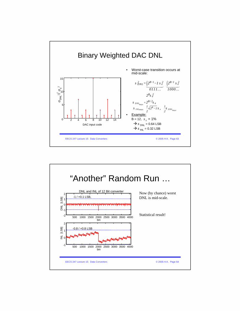
INL for Binary Weighted DAC
• INL same as for unit element DAC
• DNL depends on transition– Example:
0 to 1àσDNL2 = σ(dΙ/Ι)
2
1 to 2 àσDNL2 = 3σ(dΙ/Ι)
2
• Consider MSB transition: 0111 … à 1000 …
4 Iref Iref
Iout
2Iref2B-1 Iref
……………
EECS 247 Lecture 15: Data Converters © 2005 H.K. Page 61
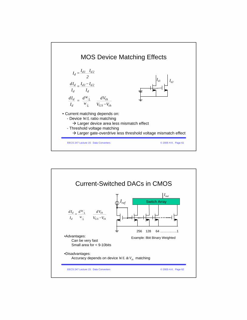
MOS Device Matching Effects
d1 d 2d
d d1 d2
d d
Wd thL
W GSd thL
I II2
dI I II I
dI d dVI V V
+=
−=
= +−
Id1 Id2
• Current matching depends on:- Device W/L ratio matching à Larger device area less mismatch effect
- Threshold voltage matchingà Larger gate-overdrive less threshold voltage mismatch effect
EECS 247 Lecture 15: Data Converters © 2005 H.K. Page 62
Current-Switched DACs in CMOS
Wd thL
Wd GS thL
dI d dV
I V V= +
−
Iout
Iref
……
Switch Array
•Advantages:Can be very fastSmall area for < 9-10bits
•Disadvantages:Accuracy depends on device W/L & Vth matching
256 128 64 ………..…..1
Example: 8bit Binary Weighted
EECS 247 Lecture 15: Data Converters © 2005 H.K. Page 63
Binary Weighted DAC DNL
( ) ( )
DNLmaxB
INL DNLmax max
2 B 1 2 B 1 2DNL
B 2
B / 2
1 12 1
2 2
2 1 2
0111... 1000...
2
2
ε
ε ε
ε
ε
σ σ σ
σ
σ σ
σ σ σ
− −
=
≅ − ≅
= − +
≅
1442443 14243
• Worst-case transition occurs at mid-scale:
• Example:B = 12, σε = 1%àσDNL = 0.64 LSBàσINL = 0.32 LSB
2 4 6 8 10 12 140
5
10
15
DAC input code
σ DN
L2 / σ ε
2
EECS 247 Lecture 15: Data Converters © 2005 H.K. Page 64
“Another” Random Run …Now (by chance) worst DNL is mid-scale.
Statistical result!500 1000 1500 2000 2500 3000 3500 4000-2
-1
0
1
2
bin
DN
L [L
SB
]
DNL and INL of 12 Bit converter
-1 / +0.1 LSB,
500 1000 1500 2000 2500 3000 3500 4000-1
0
1
2
bin
INL
[LS
B]
-0.8 / +0.8 LSB
EECS 247 Lecture 15: Data Converters © 2005 H.K. Page 65
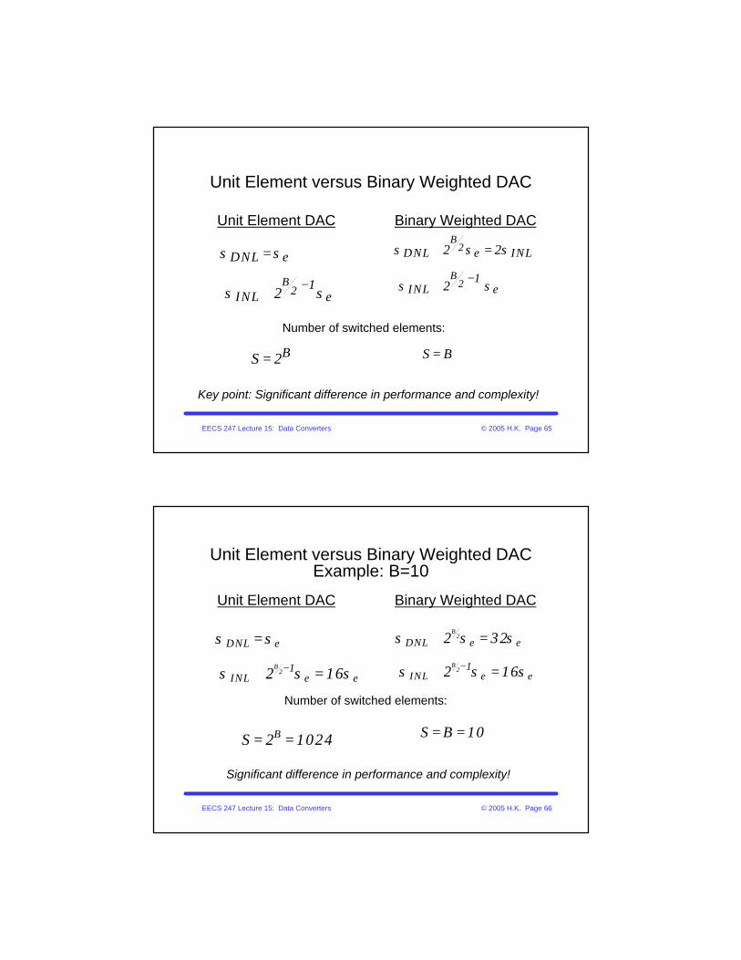
Unit Element versus Binary Weighted DAC
Unit Element DAC Binary Weighted DAC
Number of switched elements:
Key point: Significant difference in performance and complexity!
B2
B2
DNL INL
1INL
2 2
2
S B
ε
ε
σ σ σ
σ σ−
≅ =
≅
=
B2
DNL
1INL
B
2
S 2
ε
ε
σ σ
σ σ−
=
≅
=
EECS 247 Lecture 15: Data Converters © 2005 H.K. Page 66
Unit Element versus Binary Weighted DACExample: B=10
B2
DNL
1INL
B
2 16
S 2 1024
ε
ε ε
σ σ
σ σ σ−
=
≅ =
= =
Significant difference in performance and complexity!
B2
B2
DNL
1INL
2 32
2 16
S B 10
ε ε
ε ε
σ σ σ
σ σ σ−
≅ =
≅ =
= =
Unit Element DAC Binary Weighted DAC
Number of switched elements:
EECS 247 Lecture 15: Data Converters © 2005 H.K. Page 67
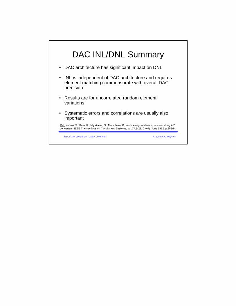
DAC INL/DNL Summary• DAC architecture has significant impact on DNL
• INL is independent of DAC architecture and requires element matching commensurate with overall DAC precision
• Results are for uncorrelated random element variations
• Systematic errors and correlations are usually also important
Ref: Kuboki, S.; Kato, K.; Miyakawa, N.; Matsubara, K. Nonlinearity analysis of resistor string A/D converters. IEEE Transactions on Circuits and Systems, vol.CAS-29, (no.6), June 1982. p.383-9.