adaptor board for std-601 - circuit design,inc
TRANSCRIPT

OG_ADP-STD-601_v1.0e 1 Circuit Design, Inc.
OPERATION GUIDE OPERATION GUIDE
Adaptor board for STD-601
ADP-A-STD601, ADP-B-STD601
Operation Guide
Version 1.0 (Jun 2018)
CIRCUIT DESIGN, INC.,
7557-1 Hotaka, Azumino-city Nagano 399-8303 JAPAN Tel: + +81-(0)263-82-1024
Fax: + +81-(0)263-82-1016
e-mail: [email protected] http://www.circuitdesign.jp

OG_ADP-STD-601_v1.0e 2 Circuit Design, Inc.
OPERATION GUIDE OPERATION GUIDE
CONTENTS
GENERAL DESCRIPTION & FEATURES ......................................... 3
General description ................................................................ 3
Features……………………………... ...................................... 3
INTRODUCTION……………….. ........................................................ 4
BOARD LAYOUT ........................................................ ………………..4
Board A Dip switch and pin identification ....... ………………..4
Board B Dip switch and pin identification ....... ………………..4
SETTING PROCEEDURE ......................................... ………………..5
Band ............................................................... ………………..5
RF Power ....................................................... ………………..5
Bit rate ............................................................ ………………..5
Channel setting .............................................. ………………..6
INTERFACE ............................................................. ………………..10
DIMENSIONS…………………………………………………………...10
CIRCUIT DIAGRAM .................................................................... …11
Board A ............................................................................ …11
Board B ........................................................................... …12
CDP-TX-02E-R, CDP-RX-02E-R COMPATIBILITY .................... …13
Introduction .................................................. ………………..13
Preparation................................................... ………………..13
Comparison between STD-601/adaptor board and
CDP module… ..................................................................... 14
RSSI acquisition ............................................................... …14
CAUTIONS & WARNINGS……………………………………………..15
REVISION HISTORY ................................................................ ...... 16

OG_ADP-STD-601_v1.0e 3 Circuit Design, Inc.
OPERATION GUIDE OPERATION GUIDE
GENERAL DESCRIPTION & FEATURES
General description
The ADP-A-STD601 (“A”) and ADP-B-STD601 (“B”) are adaptor boards that allow user to
mount the STD-601 module and perform communication tests easily while using dip
switches to set STD-601 RF bit rate, power and frequency band. By incorporating an
onboard CPU to perform the module settings, user does not need to develop setting
program and only needs to apply user data to the terminals.
The other advantage is the board’s compatibility with the existing CDP-TX-02E-R and
CDP-RX-02E-R footprint which allows current users of these modules to perform quick
test with the STD-601 without modification to their PCB.
Features
Onboard dip switches to conveniently set STD-601 band, RF power, channel and bit
rate
No need to make setting program
Useable with STD-601 400 MHz and 434 MHz *
Convert STD-601 pin layout to CDP-TX-02E-R and CDP-RX-02E-R
Board size matches those of CDP-TX-02E-R and CDP-RX-02E-R
CDP-02 module users can make communication test with STD-601 easily**.
* Both boards include STD-601 400 MHz module by default. For use with STD-601 434 MHz module please specify when ordering.
** For CDP-02 users wishing to make test with STD-601 with adaptor board, please refer to p13 – “CDP-TX-02E-R, CDP-RX-02E-R COMPATIBILITY”

OG_ADP-STD-601_v1.0e 4 Circuit Design, Inc.
OPERATION GUIDE OPERATION GUIDE
INTRODUCTION
The STD-601 is a transceiver module which consists of 2 versions, STD-601 (434 MHz) and STD-601 (400 MHz). These adaptor boards are compatible with both versions and are able to provide full transceiver operation.
By mounting the STD-601 on the boards, user only needs to set the STD-601 parameters using the dip switches to perform communication tests. A setting program does not need to be developed to set the STD-601.
BOARD LAYOUT
Board A Dip switch and pin identification
Board B Dip switch and pin identification
Data IN
Data OUT
STD-601
STD-601STD-601
STD-601 STD-601 STD-601
Board ABoard B
Board A Board A Board B Board B
Other configurations
Main configuration
Data IN
Data OUT
CPU DIP sw1 DIP sw2
DIP sw1 DIP sw2
CPU

OG_ADP-STD-601_v1.0e 5 Circuit Design, Inc.
OPERATION GUIDE OPERATION GUIDE
SETTING PROCEEDURE
Band
The STD-601 400 MHz covers 4 frequency bands. The dip switch setting is as below:
Board A and B (DIP SW 1)
Band
(MHz)
BAND-1
BAND-0
429 ON ON
447 ON OFF
458 OFF ON
434 OFF OFF
The STD-601 434 MHz covers only 434 MHz frequency band which is highlighted. If
settings for the other bands are applied while using this module, the module will not
function. Therefore the switches should remain on this setting. This also applies to RF
power and bit rate settings.
RF Power
The STD-601 400 MHz covers 4 power settings. The dip switch setting is as below:
Board A and B (DIP SW 2)
Power
(mW)
Power-1
Power-0
50 ON ON
25 ON OFF
1 OFF ON
10 OFF OFF
Bit rate
The STD-601 400 MHz covers 4 bit rate settings. The dip switch setting is as below:
Board A and B (DIP SW 2)
Bit rate
(bps)
Bit rate-1
Bitrate-0
19200 ON ON
2400 ON OFF
9600 OFF ON
4800 OFF OFF

OG_ADP-STD-601_v1.0e 6 Circuit Design, Inc.
OPERATION GUIDE OPERATION GUIDE
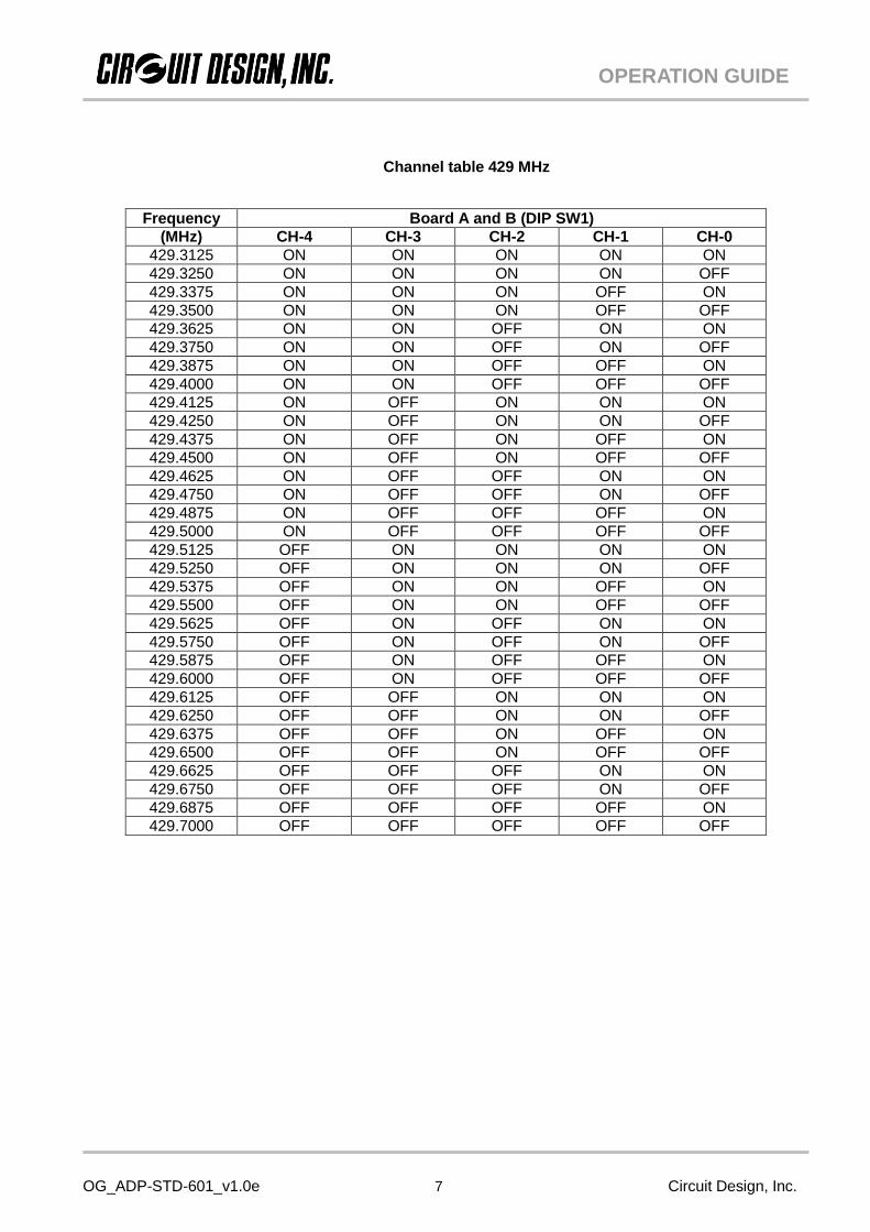
Channel setting
The CH-0 to CH-4 switches set the channel for the selected band. Refer to the frequency and channel table below:
Channel table 434 MHz
*default channel
Frequency Board A and B (DIP SW1)
(MHz) CH-4 CH-3 CH-2 CH-1 CH-0
433.875 ON ON ON ON ON
433.925 ON ON ON ON OFF
433.975 ON ON ON OFF ON
434.025 ON ON ON OFF OFF
434.075 ON ON OFF ON ON
434.125 ON ON OFF ON OFF
434.175 ON ON OFF OFF ON
434.225 ON ON OFF OFF OFF
434.275 ON OFF ON ON ON
434.325 ON OFF ON ON OFF
434.375 ON OFF ON OFF ON
434.425 ON OFF ON OFF OFF
434.475 ON OFF OFF ON ON
434.525 ON OFF OFF ON OFF
434.575 ON OFF OFF OFF ON
434.625 ON OFF OFF OFF OFF
433.900 OFF ON ON ON ON
433.950 OFF ON ON ON OFF
434.000 OFF ON ON OFF ON
434.050 OFF ON ON OFF OFF
434.100 OFF ON OFF ON ON
434.150 OFF ON OFF ON OFF
434.200 OFF ON OFF OFF ON
434.250 OFF ON OFF OFF OFF
434.300 OFF OFF ON ON ON
434.350 OFF OFF ON ON OFF
434.400 OFF OFF ON OFF ON
434.450 OFF OFF ON OFF OFF
434.500 OFF OFF OFF ON ON
434.550 OFF OFF OFF ON OFF
434.600 OFF OFF OFF OFF ON
434.650* OFF OFF OFF OFF OFF
OG_ADP-STD-601_v1.0e 7 Circuit Design, Inc.
OPERATION GUIDE OPERATION GUIDE
Channel table 429 MHz
Frequency Board A and B (DIP SW1)
(MHz) CH-4 CH-3 CH-2 CH-1 CH-0
429.3125 ON ON ON ON ON
429.3250 ON ON ON ON OFF
429.3375 ON ON ON OFF ON
429.3500 ON ON ON OFF OFF
429.3625 ON ON OFF ON ON
429.3750 ON ON OFF ON OFF
429.3875 ON ON OFF OFF ON
429.4000 ON ON OFF OFF OFF
429.4125 ON OFF ON ON ON
429.4250 ON OFF ON ON OFF
429.4375 ON OFF ON OFF ON
429.4500 ON OFF ON OFF OFF
429.4625 ON OFF OFF ON ON
429.4750 ON OFF OFF ON OFF
429.4875 ON OFF OFF OFF ON
429.5000 ON OFF OFF OFF OFF
429.5125 OFF ON ON ON ON
429.5250 OFF ON ON ON OFF
429.5375 OFF ON ON OFF ON
429.5500 OFF ON ON OFF OFF
429.5625 OFF ON OFF ON ON
429.5750 OFF ON OFF ON OFF
429.5875 OFF ON OFF OFF ON
429.6000 OFF ON OFF OFF OFF
429.6125 OFF OFF ON ON ON
429.6250 OFF OFF ON ON OFF
429.6375 OFF OFF ON OFF ON
429.6500 OFF OFF ON OFF OFF
429.6625 OFF OFF OFF ON ON
429.6750 OFF OFF OFF ON OFF
429.6875 OFF OFF OFF OFF ON
429.7000 OFF OFF OFF OFF OFF

OG_ADP-STD-601_v1.0e 8 Circuit Design, Inc.
OPERATION GUIDE OPERATION GUIDE
Channel table 458 MHz
Frequency Board A and B (DIP SW1)
(MHz) CH-4 CH-3 CH-2 CH-1 CH-0
458.5125 ON ON ON ON ON
458.5250 ON ON ON ON OFF
458.5375 ON ON ON OFF ON
458.5500 ON ON ON OFF OFF
458.5625 ON ON OFF ON ON
458.5750 ON ON OFF ON OFF
458.5875 ON ON OFF OFF ON
458.6000 ON ON OFF OFF OFF
458.6125 ON OFF ON ON ON
458.6250 ON OFF ON ON OFF
458.6375 ON OFF ON OFF ON
458.6500 ON OFF ON OFF OFF
458.6625 ON OFF OFF ON ON
458.6750 ON OFF OFF ON OFF
458.6875 ON OFF OFF OFF ON
458.7000 ON OFF OFF OFF OFF
458.7125 OFF ON ON ON ON
458.7250 OFF ON ON ON OFF
458.7375 OFF ON ON OFF ON
458.7500 OFF ON ON OFF OFF
458.7625 OFF ON OFF ON ON
458.7750 OFF ON OFF ON OFF
458.7875 OFF ON OFF OFF ON
458.8000 OFF ON OFF OFF OFF
458.8125 OFF OFF ON ON ON
458.8250 OFF OFF ON ON OFF
458.8375 OFF OFF ON OFF ON
458.8500 OFF OFF ON OFF OFF
458.8625 OFF OFF OFF ON ON
458.8750 OFF OFF OFF ON OFF
458.8875 OFF OFF OFF OFF ON
458.9000 OFF OFF OFF OFF OFF

OG_ADP-STD-601_v1.0e 9 Circuit Design, Inc.
OPERATION GUIDE OPERATION GUIDE
Channel table 447 MHz
Frequency Board A and B (DIP SW1)
(MHz) CH-4 CH-3 CH-2 CH-1 CH-0
447.5875 ON ON ON ON ON
447.6000 ON ON ON ON OFF
447.6125 ON ON ON OFF ON
447.6250 ON ON ON OFF OFF
447.6375 ON ON OFF ON ON
447.6500 ON ON OFF ON OFF
447.6625 ON ON OFF OFF ON
447.6750 ON ON OFF OFF OFF
447.6875 ON OFF ON ON ON
447.7000 ON OFF ON ON OFF
447.7125 ON OFF ON OFF ON
447.7250 ON OFF ON OFF OFF
447.7375 ON OFF OFF ON ON
447.7500 ON OFF OFF ON OFF
447.7625 ON OFF OFF OFF ON
447.7750 ON OFF OFF OFF OFF
447.7875 OFF ON ON ON ON
447.8000 OFF ON ON ON OFF
447.8125 OFF ON ON OFF ON
447.8250 OFF ON ON OFF OFF
447.8375 OFF ON OFF ON ON
447.8500 OFF ON OFF ON OFF
447.8625 OFF ON OFF OFF ON
447.8750 OFF ON OFF OFF OFF
447.8875 OFF OFF ON ON ON
447.9000 OFF OFF ON ON OFF
447.9125 OFF OFF ON OFF ON
447.9250 OFF OFF ON OFF OFF
447.9375 OFF OFF OFF ON ON
447.9500 OFF OFF OFF ON OFF
447.9625 OFF OFF OFF OFF ON
447.9750 OFF OFF OFF OFF OFF

OG_ADP-STD-601_v1.0e 10 Circuit Design, Inc.
OPERATION GUIDE OPERATION GUIDE
INTERFACE
Interface Board A Board B
ANT RF IN/OUT (Connector) RF IN/OUT (PIN)
GND GND GND
VCC 3 – 12 V 3 – 12 V
DATA IN *1
H = Vcc, L = GND H = Vcc, L = GND
DATA OUT *1
H = Vcc, L = GND H = Vcc, L = GND
TX/RX SEL OPEN=TX, GND=RX OPEN=RX, GND=TX
RSSI *2
NA Received signal strength
indicator
AF NA Demodulated signal output
Refer to STD-601 operation guide
*1 a) 2400bps, 4800bps, 9600bps, 19200bps selectable (STD-601 400 MHz) b) 4800bps, 9600bps selectable (STD-601 434 MHz)
*2 RSSI H/L indicator: Hi when received signal is higher than -90dBm.
NA - not applicable
DIMENSIONS
35.5
25.0
49.0
29.0

OG_ADP-STD-601_v1.0e 11 Circuit Design, Inc.
OPERATION GUIDE
CIRCUIT DIAGRAM
Board A
Vcc
DATA OUT
DATA IN
TX/RX SEL
GND

OG_ADP-STD-601_v1.0e 12 Circuit Design, Inc.
OPERATION GUIDE
CIRCUIT DIAGRAM
Board B
ANT
DATA OUT
GND
RSSI
Vcc
DATAIN
TX/RX
OG_ADP-STD-601_v1.0e 13 Circuit Design, Inc.
OPERATION GUIDE
OPERATION GUIDE
CDP-TX-02E-R, CDP-RX-02E-R COMPATIBILITY
Introduction
The adaptor boards have been designed to match the size and pin layout of the
CDP-TX-02E-R and CDP-RX-02E-R modules. Thus for current users of these modules, it
becomes possible to evaluate the STD-601 modules easily by replacing the CDP modules
with the adaptor boards without modifying the user PCB. The user can access other
features not covered by the CDP modules eg. selectable data rates upto 19200 bps.
As the CDP-TX-02E-R and CDP-RX-02E-R modules are designed for one way
transmission, it will not be possible to access the full transceiver functions of the STD-601
during this configuration.
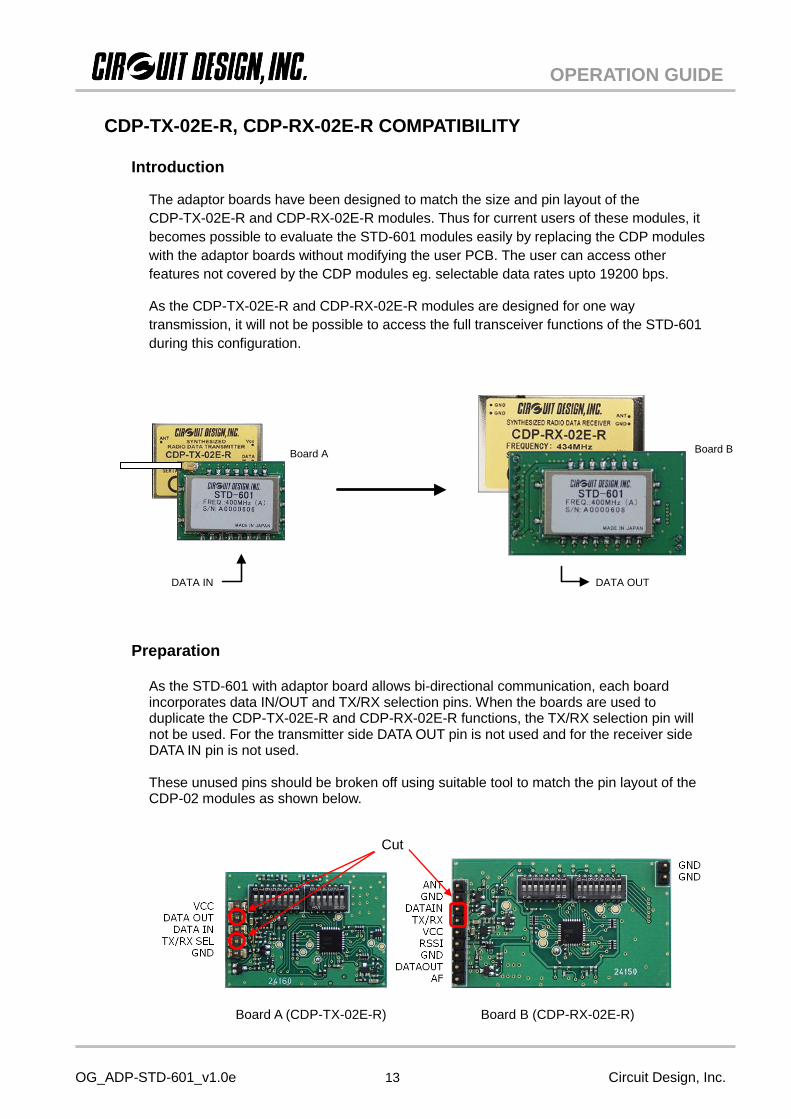
Preparation
As the STD-601 with adaptor board allows bi-directional communication, each board incorporates data IN/OUT and TX/RX selection pins. When the boards are used to duplicate the CDP-TX-02E-R and CDP-RX-02E-R functions, the TX/RX selection pin will not be used. For the transmitter side DATA OUT pin is not used and for the receiver side DATA IN pin is not used. These unused pins should be broken off using suitable tool to match the pin layout of the CDP-02 modules as shown below.
Board A (CDP-TX-02E-R) Board B (CDP-RX-02E-R)
DATA IN DATA OUT
Board A Board B
Cut

OG_ADP-STD-601_v1.0e 14 Circuit Design, Inc.
OPERATION GUIDE OPERATION GUIDE
Comparison between STD-601 / adaptor board and CDP module
Comparison between CDP-TX-02E-R and adaptor board A (transmitter)
Interface pin CDP-TX-02E-R STD-601 / Adaptor board A
VCC 3 – 12 V -> 3 – 12 V
Data IN Max. 4800 bps -> Selectable *1
GND GND -> GND
Comparison between CDP-RX-02E-R and adaptor board B (receiver)
Interface pin CDP-RX-02E-R STD-601 / Adaptor board B
ANT RF In -> RF In
GND GND -> GND
VCC 3 – 12 V -> 3 – 12 V
RSSI Received signal strength (Analogue)
-> Received signal strength (H/L) *2
GND GND -> GND
DATA OUT Max. 4800 bps -> Selectable *1
AF Demodulated signal output
-> NA (Not available)
*1 a) 2400bps, 4800bps, 9600bps, 19200bps selectable (STD-601 400 MHz) b) 4800bps, 9600bps selectable (STD-601 434 MHz) *2 RSSI H/L indicator: Hi when received signal is higher than -90dBm.
RSSI acquisition
The CDP-RX-02E-R is able to provide RSSI output in the form of an analogue voltage. When using the adaptor board, the RSSI pin will not output analogue voltage but instead output a digital HIGH and LOW signal when the RSSI crosses a set threshold (-90dBm).

OG_ADP-STD-601_v1.0e 15 Circuit Design, Inc.
OPERATION GUIDE OPERATION GUIDE
Cautions
As the product communicates using electronic radio waves, there are cases where transmission will be
temporarily cut off due to the surrounding environment and method of usage. The manufacturer is exempt from
all responsibility relating to resulting harm to personnel or equipment and other secondary damage.
Do not use the equipment within the vicinity of devices that may malfunction as a result of electronic radio waves
from the product.
The manufacturer is exempt from all responsibility relating to secondary damage resulting from the operation,
performance and reliability of equipment connected to the product.
Communication performance will be affected by the surrounding environment, so communication tests should be
carried out before actual use.
Ensure that the power supply for the product is within the specified rating. Short circuits and reverse connections
may result in overheating and damage and must be avoided at all costs.
Ensure that the power supply has been switched off before attempting any wiring work.
The case is connected to the GND terminal of the internal circuit, so do not make contact between the '+' side of
the power supply terminal and the case.
When batteries are used as the power source, avoid short circuits, recharging, dismantling, and pressure.
Failure to observe this caution may result in the outbreak of fire, overheating and damage to the equipment.
Remove the batteries when the equipment is not to be used for a long period of time. Failure to observe this
caution may result in battery leaks and damage to the equipment.
Do not use this product in vehicles with the windows closed, in locations where it is subject to direct sunlight, or
in locations with extremely high humidity.
The product is neither waterproof nor splash proof. Ensure that it is not splashed with soot or water. Do not use
the equipment if water or other foreign matter has entered the case.
Do not drop the product or otherwise subject it to strong shocks.
Do not subject the equipment to condensation (including moving it from cold locations to locations with a
significant increase in temperature.)
Do not use the equipment in locations where it is likely to be affected by acid, alkalis, organic agents or corrosive
gas.
The GND for the product will also affect communication performance. If possible, ensure that the case GND and
the circuit GND are connected to a large GND pattern.
Warnings
Do not take apart or modify the equipment.
Do not remove the product label (the label attached to the upper surface of the product.) Using a product from
which the label has been removed is prohibited.
Circuit Design, Inc. All right reserved
No part of this document may be copied or distributed in part or in whole without the prior written consent of Circuit Design, Inc. Customers are advised to consult with Circuit Design sales representatives before ordering. Circuit Design, Inc. believes the furnished information is accurate and reliable. However, Circuit Design, Inc. reserves the right to make changes to this product without notice.

OG_ADP-STD-601_v1.0e 16 Circuit Design, Inc.
OPERATION GUIDE OPERATION GUIDE
REVISION HISTORY
Version Date Description Remark
1.0 Jun. 2018 The first issue