ad adc84/ad adc85 fast, complete 12-bit a/d converters ... · composition type is generally...
TRANSCRIPT

Fast, Complete 12-Bit A/D Converters
AD ADC84/AD ADC85
Rev. B Information furnished by Analog Devices is believed to be accurate and reliable. However, no responsibility is assumed by Analog Devices for its use, nor for any infringements of patents or other rights of third parties that may result from its use. Specifications subject to change without notice. No license is granted by implication or otherwise under any patent or patent rights of Analog Devices. Trademarks and registered trademarks are the property of their respective owners.
One Technology Way, P.O. Box 9106, Norwood, MA 02062-9106, U.S.A. Tel: 781.329.4700 www.analog.com Fax: 781.326.8703 © 2003 Analog Devices, Inc. All rights reserved.
FEATURES PERFORMANCE Complete 12-bit A/D converter with reference and clock Fast successive approximation conversion: 10 µs or 5 µs Buried Zener reference for long-term stability and low
Gain TC: 10 ppm/°C Max nonlinearity: < ±0.012% Low power: 880 mW typ Low chip count—high reliability Industry-standard pinout Z models for ±12 V operation available MIL-STD-883B processing available
VERSATILITY Negative true parallel logic outputs Short cycle capability Precision +6.3 V reference for external applications
PRODUCT DESCRIPTION
The AD ADC84/AD ADC85 series devices are high speed, low cost 12-bit successive approximation analog-to-digital converters that include an internal clock, reference, and comparator. Its hybrid IC design utilizes MSI digital and linear monolithic chips in conjunction with a 12-bit monolithic DAC to provide modular performance and versatility with IC size, price, and reliability.
Important performance characteristics of the AD ADC84/ AD ADC85 series include maximum linearity error of ±0.012%; gain TC below 15 ppm/°C at 25°C; typical power dissipation of 880 mW; and conversion time of less than 10 µs for the 12-bit versions. Of considerable significance in severe and aerospace applications is the guaranteed performance from –55°C to +125°C of the AD ADC85S, which is also available with environmental screening. Monotonic operation of the feedback DAC guarantees no missing codes over temperature ranges of 0°C to +70°C, –25°C to +85°C, and –55°C to +125°C.
The design of the AD ADC84/AD ADC85 includes scaling resistors that provide analog input signal ranges of ±2.5 V, ±5 V, ±10 V, 0 V to +5 V, or 0 V to +10 V. The 6.3 V precision reference, which can be used for external applications, and the input buffer amplifier add flexibility and value. All digital signals are fully DTL and TTL compatible, and the data output is negative-true and available in parallel form.
The AD ADC84/AD ADC85 are available in a performance grade specified for 12-bit accuracy (±0.012% FSR max) with 10 µs maximum conversion time.
Figure 1. Functional Block Diagram
The AD ADC84 and AD ADC85C are specified for operation over the 0°C to +70°C temperature range. The AD ADC85 and AD ADC85S are specified for the –25°C to +85°C and –55°C to +125°C ranges, respectively. The serial output function is no longer supported on the AD ADC84/AD ADC85 after date code 9623.
PRODUCT HIGHLIGHTS
1. The AD ADC84/ AD ADC85 series devices are complete 12-bit ADCs. No external components are required to perform a conversion.
2. The AD ADC84/ AD ADC85 directly replaces other devices of this type with significant increases in performance.
3. The fast conversion rates of the AD ADC84 and AD ADC85 (10 μs) make them an excellent choice for applications requiring high system throughput rates.
4. The internal buried Zener reference is laser trimmed to 6.3 V ±0.1% and ±10 ppm/°C typical TC. The reference is available externally and can provide up to 1 mA.
5. The integrated package construction provides high quality and reliability with small size and weight.
6. The monolithic 12-bit feedback DAC is used for reduced chip count and higher reliability.
7. The AD ADC85S/883B comes processed to MIL-STD-883, Class B requirements.

AD ADC84/AD ADC85
Rev. B | Page 2 of 12
TABLE OF CONTENTS Specifications..................................................................................... 3
Typical Performance Characteristics ............................................. 5
Functional Description .................................................................... 6
Offset Adjustment ........................................................................ 6
Gain Adjustment........................................................................... 6
Theory of Operation .................................................................... 6
Timing............................................................................................ 6
Digital Output Data ..................................................................... 7
Input Scaling ..................................................................................8
Input Voltage Range and LSB Values ..........................................8
Calibration......................................................................................9
Grounding ......................................................................................9
Clock Rate Control Alternate Connections............................ 10
Microprocessor Interfacing....................................................... 10
Outline Dimensions ....................................................................... 11
Ordering Guide .......................................................................... 11
REVISION HISTORY
Revision B 11/03—Data Sheet changed from Rev. A to Rev. B
Removed AD5240...............................................................Universal
Updated format...................................................................Universal
Added text to PRODUCT DESCRIPTION .................................. 1
Updated OUTLINE DIMENSIONS ............................................ 11
AD ADC84/AD ADC85
Rev. B | Page 3 of 12
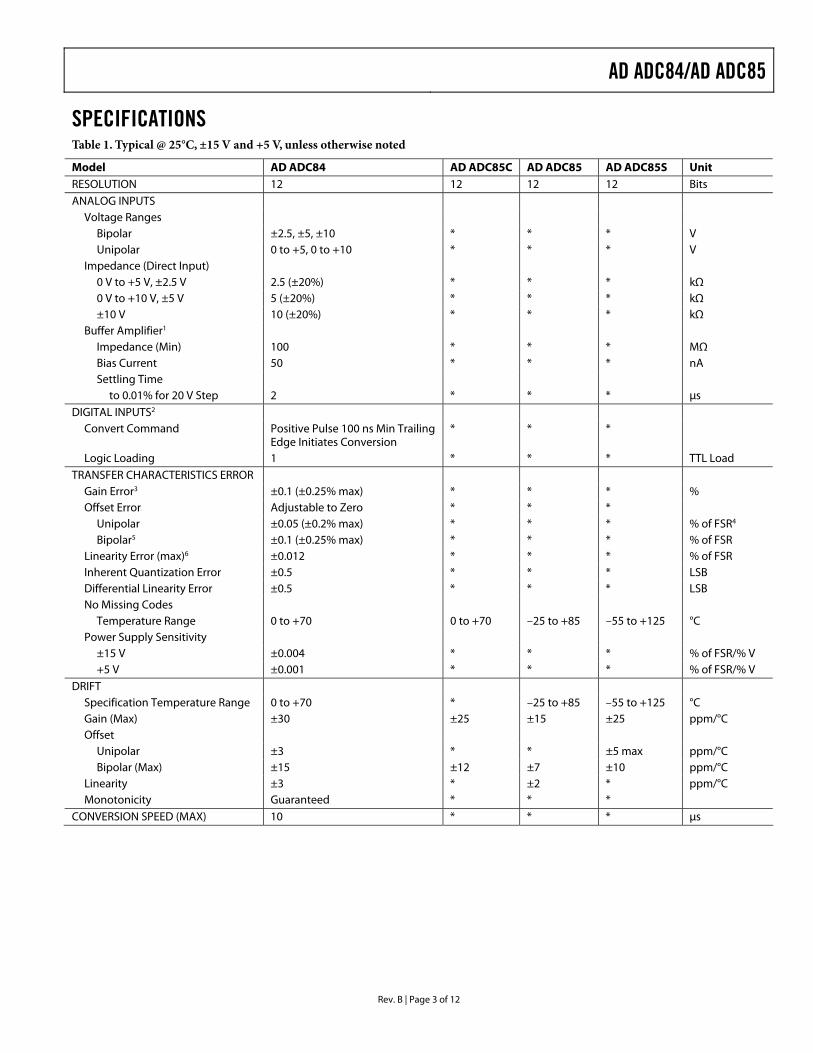
SPECIFICATIONS Table 1. Typical @ 25°C, ±15 V and +5 V, unless otherwise noted
Model AD ADC84 AD ADC85C AD ADC85 AD ADC85S Unit RESOLUTION 12 12 12 12 Bits ANALOG INPUTS
Voltage Ranges Bipolar ±2.5, ±5, ±10 * * * V Unipolar 0 to +5, 0 to +10 * * * V
Impedance (Direct Input) 0 V to +5 V, ±2.5 V 2.5 (±20%) * * * kΩ 0 V to +10 V, ±5 V 5 (±20%) * * * kΩ ±10 V 10 (±20%) * * * kΩ
Buffer Amplifier1 Impedance (Min) 100 * * * MΩ Bias Current 50 * * * nA Settling Time
to 0.01% for 20 V Step 2 * * * µs DIGITAL INPUTS2
Convert Command Positive Pulse 100 ns Min Trailing Edge Initiates Conversion
* * *
Logic Loading 1 * * * TTL Load TRANSFER CHARACTERISTICS ERROR
Gain Error3 ±0.1 (±0.25% max) * * * % Offset Error3 Adjustable to Zero * * *
Unipolar ±0.05 (±0.2% max) * * * % of FSR4
Bipolar5 ±0.1 (±0.25% max) * * * % of FSR Linearity Error (max)6 ±0.012 * * * % of FSR Inherent Quantization Error ±0.5 * * * LSB Differential Linearity Error ±0.5 * * * LSB No Missing Codes
Temperature Range 0 to +70 0 to +70 –25 to +85 –55 to +125 °C Power Supply Sensitivity
±15 V ±0.004 * * * % of FSR/% V +5 V ±0.001 * * * % of FSR/% V
DRIFT Specification Temperature Range 0 to +70 * –25 to +85 –55 to +125 °C Gain (Max) ±30 ±25 ±15 ±25 ppm/°C Offset
Unipolar ±3 * * ±5 max ppm/°C Bipolar (Max)5 ±15 ±12 ±7 ±10 ppm/°C
Linearity ±3 * ±2 * ppm/°C Monotonicity Guaranteed * * *
CONVERSION SPEED (MAX) 10 * * * µs
AD ADC84/AD ADC85
Rev. B | Page 4 of 12
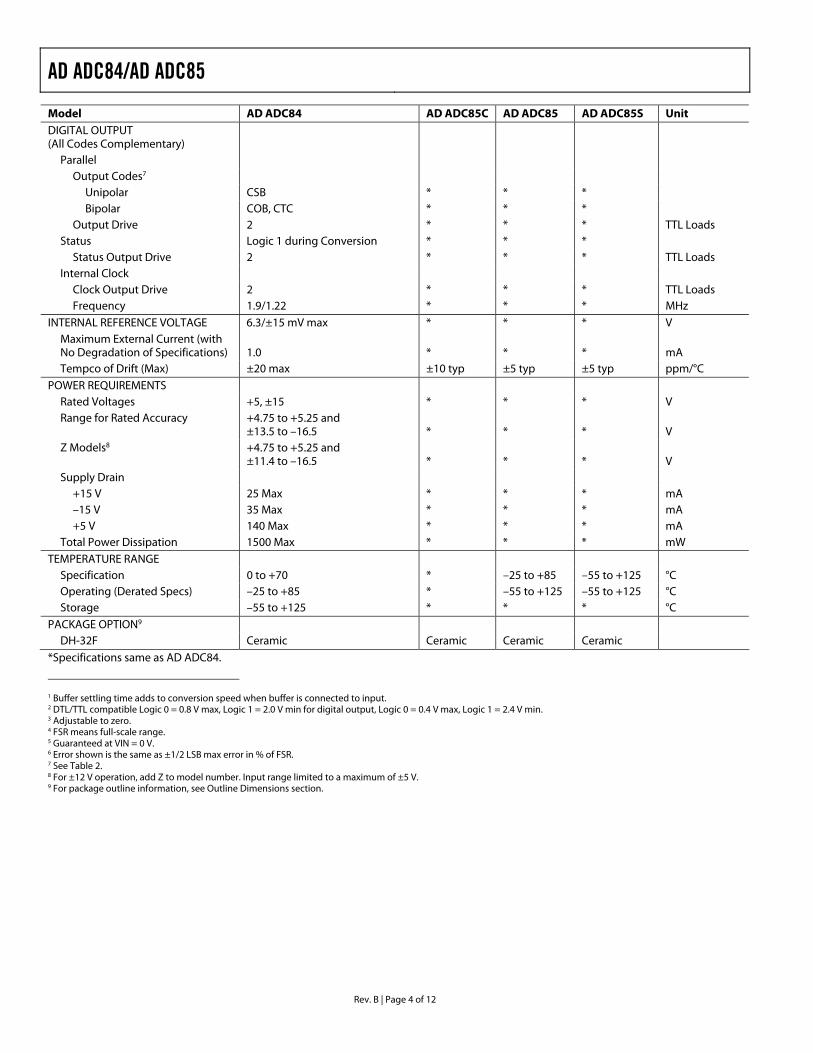
Model AD ADC84 AD ADC85C AD ADC85 AD ADC85S Unit DIGITAL OUTPUT (All Codes Complementary)
Parallel Output Codes7
Unipolar CSB * * * Bipolar COB, CTC * * *
Output Drive 2 * * * TTL Loads Status Logic 1 during Conversion * * *
Status Output Drive 2 * * * TTL Loads Internal Clock
Clock Output Drive 2 * * * TTL Loads Frequency 1.9/1.22 * * * MHz
INTERNAL REFERENCE VOLTAGE 6.3/±15 mV max * * * V Maximum External Current (with No Degradation of Specifications) 1.0 * * * mA Tempco of Drift (Max) ±20 max ±10 typ ±5 typ ±5 typ ppm/°C
POWER REQUIREMENTS Rated Voltages +5, ±15 * * * V Range for Rated Accuracy +4.75 to +5.25 and
±13.5 to –16.5 * * * V Z Models8 +4.75 to +5.25 and
±11.4 to –16.5 * * * V Supply Drain
+15 V 25 Max * * * mA –15 V 35 Max * * * mA +5 V 140 Max * * * mA
Total Power Dissipation 1500 Max * * * mW TEMPERATURE RANGE
Specification 0 to +70 * –25 to +85 –55 to +125 °C Operating (Derated Specs) –25 to +85 * –55 to +125 –55 to +125 °C Storage –55 to +125 * * * °C
PACKAGE OPTION9 DH-32F Ceramic Ceramic Ceramic Ceramic
*Specifications same as AD ADC84.
1 Buffer settling time adds to conversion speed when buffer is connected to input. 2 DTL/TTL compatible Logic 0 = 0.8 V max, Logic 1 = 2.0 V min for digital output, Logic 0 = 0.4 V max, Logic 1 = 2.4 V min. 3 Adjustable to zero. 4 FSR means full-scale range. 5 Guaranteed at VIN = 0 V. 6 Error shown is the same as ±1/2 LSB max error in % of FSR. 7 See Table 2. 8 For ±12 V operation, add Z to model number. Input range limited to a maximum of ±5 V. 9 For package outline information, see Outline Dimensions section.

AD ADC84/AD ADC85
Rev. B | Page 5 of 12
TYPICAL PERFORMANCE CHARACTERISTICS
Figure 2. Linearity Error vs. Conversion Speed
Figure 3. Gain Drift Error (%FSR) vs. Temperature
Figure 4. Change in Differential Linearity vs. Conversion Speed
Figure 5. Conversion Speed vs. Control Voltage

AD ADC84/AD ADC85
Rev. B | Page 6 of 12
FUNCTIONAL DESCRIPTION OFFSET ADJUSTMENT The zero adjust circuit consists of a potentiometer connected across ±VS with its slider connected through a 1.8 MΩ resistor to Comparator Input Pin 22 for all ranges. As shown in Figure 6, the tolerance of this fixed resistor is not critical, and a carbon composition type is generally adequate. Using a carbon composition resistor having a –1200 ppm/°C tempco contrib-utes a worst-case offset tempco of 8 × 244 × 10–6 × 1200 ppm/°C = 2.3 ppm/°C of FSR, if the OFFSET ADJ potentiometer is set at either end of its adjustment range. Since the maximum offset adjustment required is typically no more than ±4 LSB, use of a carbon composition offset summing resistor typically contributes no more than 1 ppm/°C of FSR offset tempco.
Figure 6. Offset Adjustment Circuit
An alternate offset adjust circuit, which contributes negligible offset tempco if metal film resistors (tempco <100 ppm/°C) are used, is shown in Figure 7.
Figure 7. Low Tempco Zero Adjustment Circuit
In either zero adjust circuit, the fixed resistor connected to Pin 22 should be located close to this pin to keep the pin connection runs short. (Comparator Input Pin 22 is quite sensitive to external noise pickup).
GAIN ADJUSTMENT The gain adjust circuit consists of a potentiometer connected across ±VS with its slider connected through a 10MΩ resistor to the Gain Adjust pin 27 as shown in Figure 8.
Figure 8. Gain Adjustment Circuit
An alternate gain adjust circuit which contributes negligible gain tempco if metal film resistors (Tempco < 100 ppm/°C) are used is shown in Figure 9.
Figure 9. Low Tempco G
ain Adjustment Circuit
84/
he
eriod, depending on the comparator at that time.
ata
alid on the same
ta
er to be initiated by the trailing dge of the STATUS signal.
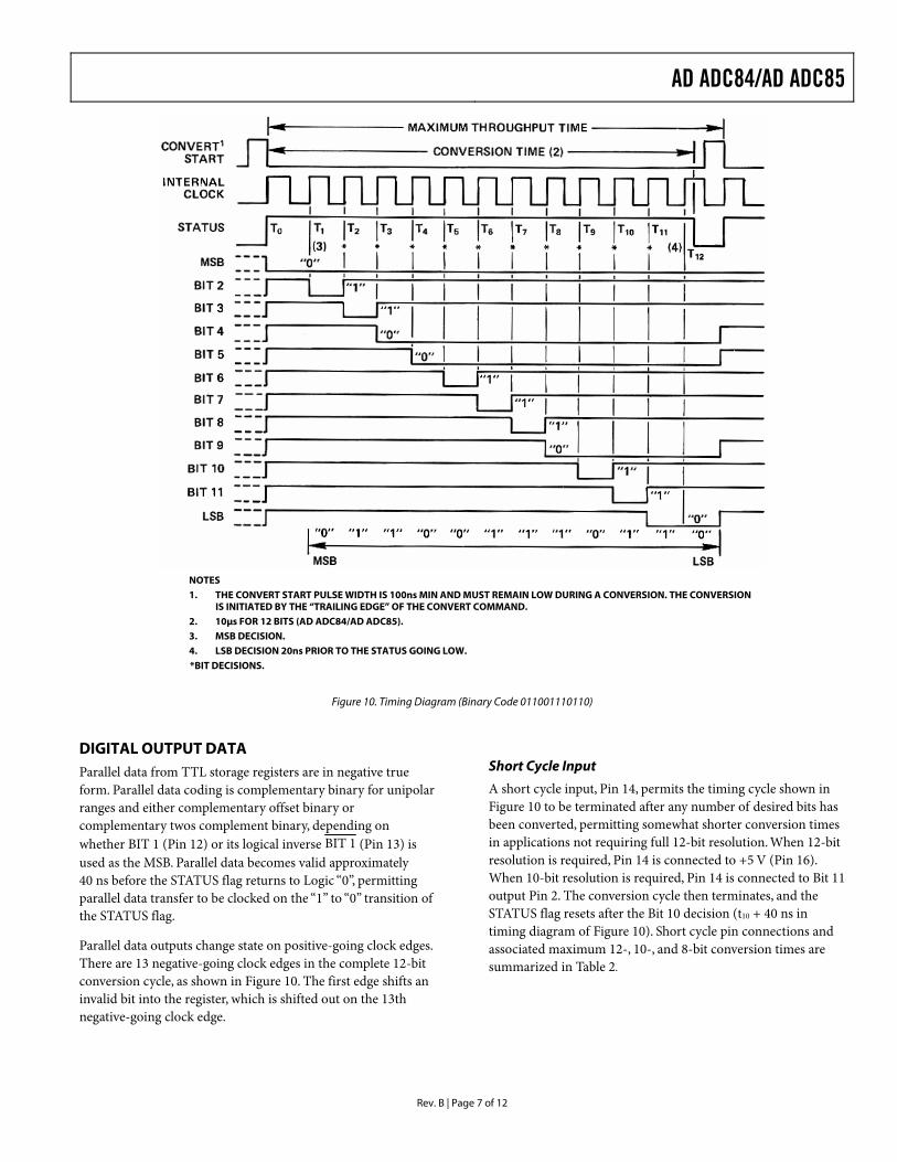
THEORY OF OPERATION On receipt of a CONVERT START command, the AD ADCAD ADC85 converts the voltage as its analog input into an equivalent 12-bit binary number. This conversion is accomplished as follows: The 12-bit successive approximation register (SAR) has its 12-bit outputs connected both to the device bit output pins and to the corresponding bit inputs of the feedback DAC. The analog input is successively compared to tfeedback DAC output, one bit at a time (MSB first, LSB last). The decision to keep or reject each bit is then made at the completion of each bit comparison pstate of the
TIMING The timing diagram is shown in Figure 10. Receipt of a CONVERT START signal sets the STATUS flag, indicatingconversion in progress. This, in turn, removes the inhibit applied to the gated clock, permitting it to run through 13 cycles. All the SAR parallel bits, STATUS flip-flops, and the gated clock inhibit signal are initialized on the trailing edge of the CONVERT START signal. At time t0, Bit 1 is reset and Bit 2 to Bit 12 are set unconditionally. At t1, the Bit 1 decision is made (keep) and Bit 2 is unconditionally reset. At t2, the Bit 2 decision is made (keep) and Bit 3 is reset unconditionally. This sequencecontinues until the Bit 12 (LSB) decision (keep) is made at t12. After a 40 ns delay period, the STATUS flag is reset, indicating that the conversion is complete and that the parallel output dis valid. Resetting the STATUS flag restores the gated clock inhibit signal, forcing the clock output to the Logic 0 state.
Corresponding parallel data bits become vpositive-going clock edge (see Figure 10).
Incorporation of the 40ns delay guarantees that the parallel dais valid at the Logic 1 to 0 transition of the STATUS flag, permitting parallel data transfe
AD ADC84/AD ADC85
Rev. B | Page 7 of 12
NOTES 1. THE CONVERT START PULSE WIDTH IS 100ns MIN AND MUST REMAIN LOW DURING A CONVERSION. THE CONVERSION
IS INITIATED BY THE “TRAILING EDGE” OF THE CONVERT COMMAND. 2. 10μs FOR 12 BITS (AD ADC84/AD ADC85). 3. MSB DECISION. 4. LSB DECISION 20ns PRIOR TO THE STATUS GOING LOW.
*BIT DECISIONS.
Figure 10. Timing Diagram (Binary Code 011001110110)
DIGITAL OUTPUT DATA Parallel data from TTL storage registers are in negative true form. Parallel data coding is complementary binary for unipolar ranges and either complementary offset binary or complementary twos complement binary, depending on whether BIT 1 (Pin 12) or its logical inverse BIT 1 (Pin 13) is used as the MSB. Parallel data becomes valid approximately 40 ns before the STATUS flag returns to Logic “0”, permitting parallel data transfer to be clocked on the “1” to “0” transition of the STATUS flag.
Parallel data outputs change state on positive-going clock edges. There are 13 negative-going clock edges in the complete 12-bit conversion cycle, as shown in Figure 10. The first edge shifts an invalid bit into the register, which is shifted out on the 13th negative-going clock edge.
Short Cycle Input
A short cycle input, Pin 14, permits the timing cycle shown in Figure 10 to be terminated after any number of desired bits has been converted, permitting somewhat shorter conversion times in applications not requiring full 12-bit resolution. When 12-bit resolution is required, Pin 14 is connected to +5 V (Pin 16). When 10-bit resolution is required, Pin 14 is connected to Bit 11 output Pin 2. The conversion cycle then terminates, and the STATUS flag resets after the Bit 10 decision (t10 + 40 ns in timing diagram of Figure 10). Short cycle pin connections and associated maximum 12-, 10-, and 8-bit conversion times are summarized in Table 2.
AD ADC84/AD ADC85
Rev. B | Page 8 of 12
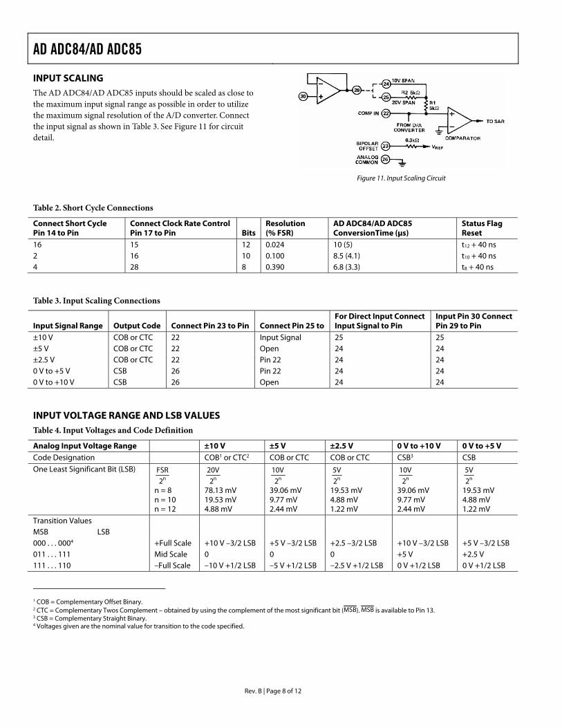
INPUT SCALING The AD ADC84/AD ADC85 inputs should be scaled as close to the maximum input signal range as possible in order to utilize the maximum signal resolution of the A/D converter. Connect the input signal as shown in Table 3. See Figure 11 for circuit detail.
Figure 11. Input Scaling Circuit
Table 2. Short Cycle Connections
Connect Short Cycle Pin 14 to Pin
Connect Clock Rate Control Pin 17 to Pin Bits
Resolution (% FSR)
AD ADC84/AD ADC85 ConversionTime (μs)
Status Flag Reset
16 15 12 0.024 10 (5) t12 + 40 ns 2 16 10 0.100 8.5 (4.1) t10 + 40 ns 4 28 8 0.390 6.8 (3.3) t8 + 40 ns
Table 3. Input Scaling Connections
Input Signal Range Output Code Connect Pin 23 to Pin Connect Pin 25 to For Direct Input Connect Input Signal to Pin
Input Pin 30 Connect Pin 29 to Pin
±10 V COB or CTC 22 Input Signal 25 25 ±5 V COB or CTC 22 Open 24 24 ±2.5 V COB or CTC 22 Pin 22 24 24 0 V to +5 V CSB 26 Pin 22 24 24 0 V to +10 V CSB 26 Open 24 24
INPUT VOLTAGE RANGE AND LSB VALUES Table 4. Input Voltages and Code Definition
Analog Input Voltage Range ±10 V ±5 V ±2.5 V 0 V to +10 V 0 V to +5 V Code Designation COB1 or CTC2 COB or CTC COB or CTC CSB3 CSB One Least Significant Bit (LSB)
n2
FSR
n = 8 n = 10 n = 12
n2
20V
78.13 mV 19.53 mV 4.88 mV
n2
10V
39.06 mV 9.77 mV 2.44 mV
n2
5V
19.53 mV 4.88 mV 1.22 mV
n2
10V
39.06 mV 9.77 mV 2.44 mV
n2
5V
19.53 mV 4.88 mV 1.22 mV
Transition Values MSB LSB 000 . . . 0004 +Full Scale +10 V –3/2 LSB +5 V –3/2 LSB +2.5 –3/2 LSB +10 V –3/2 LSB +5 V –3/2 LSB 011 . . . 111 Mid Scale 0 0 0 +5 V +2.5 V 111 . . . 110 –Full Scale –10 V +1/2 LSB –5 V +1/2 LSB –2.5 V +1/2 LSB 0 V +1/2 LSB 0 V +1/2 LSB
1 COB = Complementary Offset Binary. 2 CTC = Complementary Twos Complement – obtained by using the complement of the most significant bit (MSB). MSB is available to Pin 13. 3 CSB = Complementary Straight Binary. 4 Voltages given are the nominal value for transition to the code specified.
AD ADC84/AD ADC85
Rev. B | Page 9 of 12
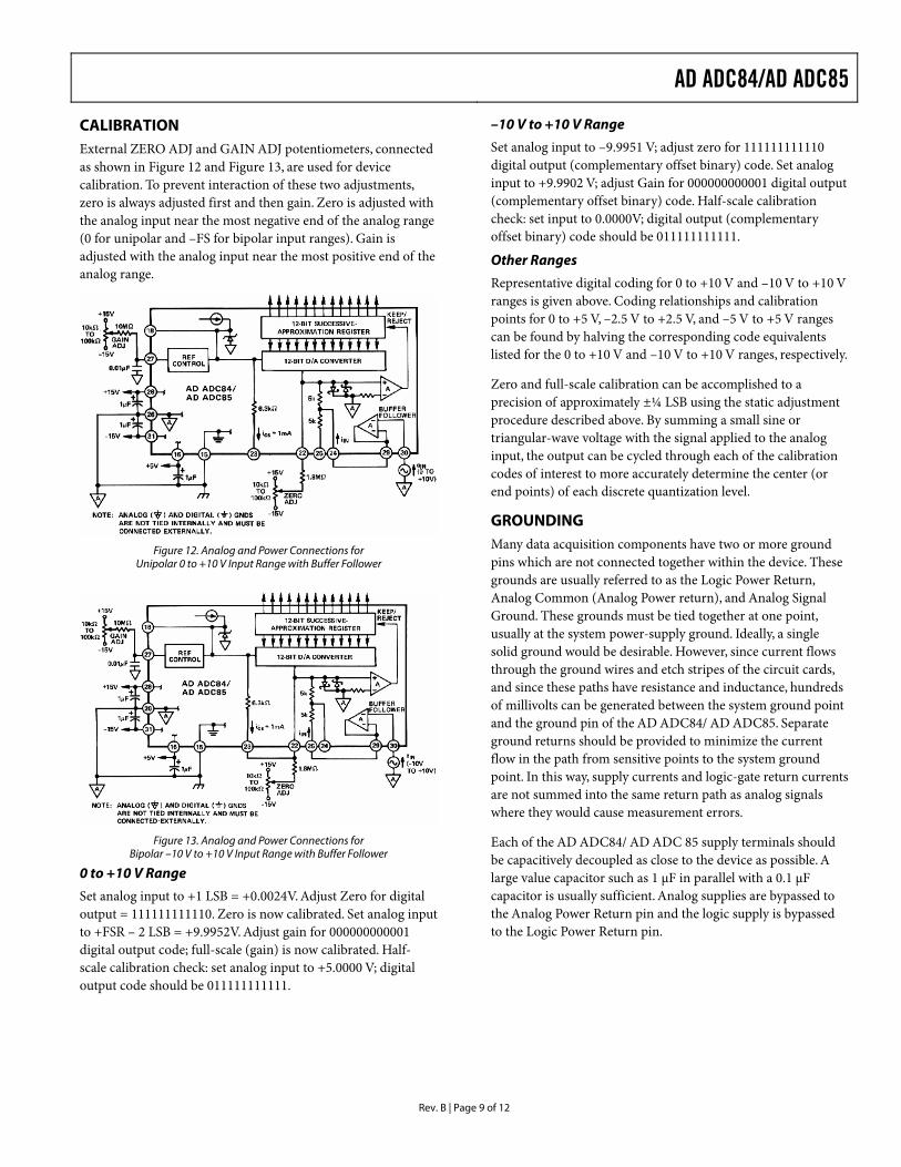
CALIBRATION External ZERO ADJ and GAIN ADJ potentiometers, connected as shown in Figure 12 and Figure 13, are used for device calibration. To prevent interaction of these two adjustments, zero is always adjusted first and then gain. Zero is adjusted with the analog input near the most negative end of the analog range (0 for unipolar and –FS for bipolar input ranges). Gain is adjusted with the analog input near the most positive end of the analog range.
Figure 12. Analog and Power Connections for Unipolar 0 to +10 V Input Range with Buffer Follower
Figure 13. Analog and Power Connections for Bipolar –10 V to +10 V Input Range with Buffer Follower
0 to +10 V Range
Set analog input to +1 LSB = +0.0024V. Adjust Zero for digital output = 111111111110. Zero is now calibrated. Set analog input to +FSR – 2 LSB = +9.9952V. Adjust gain for 000000000001 digital output code; full-scale (gain) is now calibrated. Half-scale calibration check: set analog input to +5.0000 V; digital output code should be 011111111111.
–10 V to +10 V Range
Set analog input to –9.9951 V; adjust zero for 111111111110 digital output (complementary offset binary) code. Set analog input to +9.9902 V; adjust Gain for 000000000001 digital output (complementary offset binary) code. Half-scale calibration check: set input to 0.0000V; digital output (complementary offset binary) code should be 011111111111.
Other Ranges
Representative digital coding for 0 to +10 V and –10 V to +10 V ranges is given above. Coding relationships and calibration points for 0 to +5 V, –2.5 V to +2.5 V, and –5 V to +5 V ranges can be found by halving the corresponding code equivalents listed for the 0 to +10 V and –10 V to +10 V ranges, respectively.
Zero and full-scale calibration can be accomplished to a precision of approximately ±¼ LSB using the static adjustment procedure described above. By summing a small sine or triangular-wave voltage with the signal applied to the analog input, the output can be cycled through each of the calibration codes of interest to more accurately determine the center (or end points) of each discrete quantization level.
GROUNDING Many data acquisition components have two or more ground pins which are not connected together within the device. These grounds are usually referred to as the Logic Power Return, Analog Common (Analog Power return), and Analog Signal Ground. These grounds must be tied together at one point, usually at the system power-supply ground. Ideally, a single solid ground would be desirable. However, since current flows through the ground wires and etch stripes of the circuit cards, and since these paths have resistance and inductance, hundreds of millivolts can be generated between the system ground point and the ground pin of the AD ADC84/ AD ADC85. Separate ground returns should be provided to minimize the current flow in the path from sensitive points to the system ground point. In this way, supply currents and logic-gate return currents are not summed into the same return path as analog signals where they would cause measurement errors.
Each of the AD ADC84/ AD ADC 85 supply terminals should be capacitively decoupled as close to the device as possible. A large value capacitor such as 1 µF in parallel with a 0.1 µF capacitor is usually sufficient. Analog supplies are bypassed to the Analog Power Return pin and the logic supply is bypassed to the Logic Power Return pin.

AD ADC84/AD ADC85
Rev. B | Page 10 of 12
CLOCK RATE CONTROL ALTERNATE CONNECTIONS If adjustment of the CLOCK RATE is desired for faster conver-sion speeds, the CLOCK RATE CONTROL may be connected to an external multiturn trim potentiometer with a TCR of ±100 ppm/°C or less as shown in Figure 14 and Figure 15. If the potentiometer is connected to –15 V, conversion time can be increased as shown in Figure 5. If these adjustments are used, delete the connections shown in Table 2 for Pin 17. See Figure 2 for nonlinearity error versus conversion speed and Figure 5 for the effect of the control voltage on clock speed.
Figure 14. 12-Bit Clock Rate Control Optional Fine Adjust
Figure 15. 8-Bit Clock Rate Control Optional Fine Adjust
MICROPROCESSOR INTERFACING The fast conversion times of the AD ADC84/AD ADC85 suggests several methods of interface to microprocessors. In systems where the ADC is used for high sampling rates on a single signal which is to be digitally processed, CPU-controlled conversion may be inefficient due to the slow cycle times of most microprocessors. It is generally preferable to perform conversions independently, inserting the resultant digital data directly into memory. This can be done using direct memory access (DMA), which is totally transparent to the CPU. Interface to user-designed DMA hardware is facilitated by the guaranteed data validity on the falling edge of the EOC signal.
Clearly, 12 bits of data must be broken up for interface to a 8-bit wide data bus. There are two possible formats: right-justified and left-justified. In a right-justified system, the least significant 8 bits occupy one byte and the four MSBs reside in the low nibble of another byte. This format is useful when the data from the ADC is being treated as a binary number between 0 and 4095. The left-justified format supplies the eight most-
significant bits in one byte and the 4 LSBs in the high nibble of another byte. The data now represents the fractional binary number relating the analog signal to the full-scale voltage. An advantage to this organization is that the most-significant eight bits can be read by the processor as a coarse indication of the true signal value. The full 12-bit word can then be read only when all 12 bits are needed. This allows faster and more efficient control of a process.
Figure 16 shows a typical connection of 8085-type bus, using a left-justified data format for unipolar inputs. Status polling is optional, and can be read simultaneously with the 4LSBs. If it is desired to right-justify the data, pins 1 through 12 of the ADADC84/AD ADC85 should be reversed, as well as the connections to the data bus high and low byte address signals.
When dealing with bipolar inputs (±5V, ±10V ranges), using the MSB directly yields a complementary offset binary-coded output. If complementary twos complement coding is desired, it can be produced be substituting MSB (Pin 13) for the MSB. This facilitates the arithmetic operation which are subsequently performed on the ADC output data.
Figure 16. AD ADC84/AD ADC85 – 8085A Interface Connections
AD ADC84/AD ADC85
Rev. B | Page 11 of 12
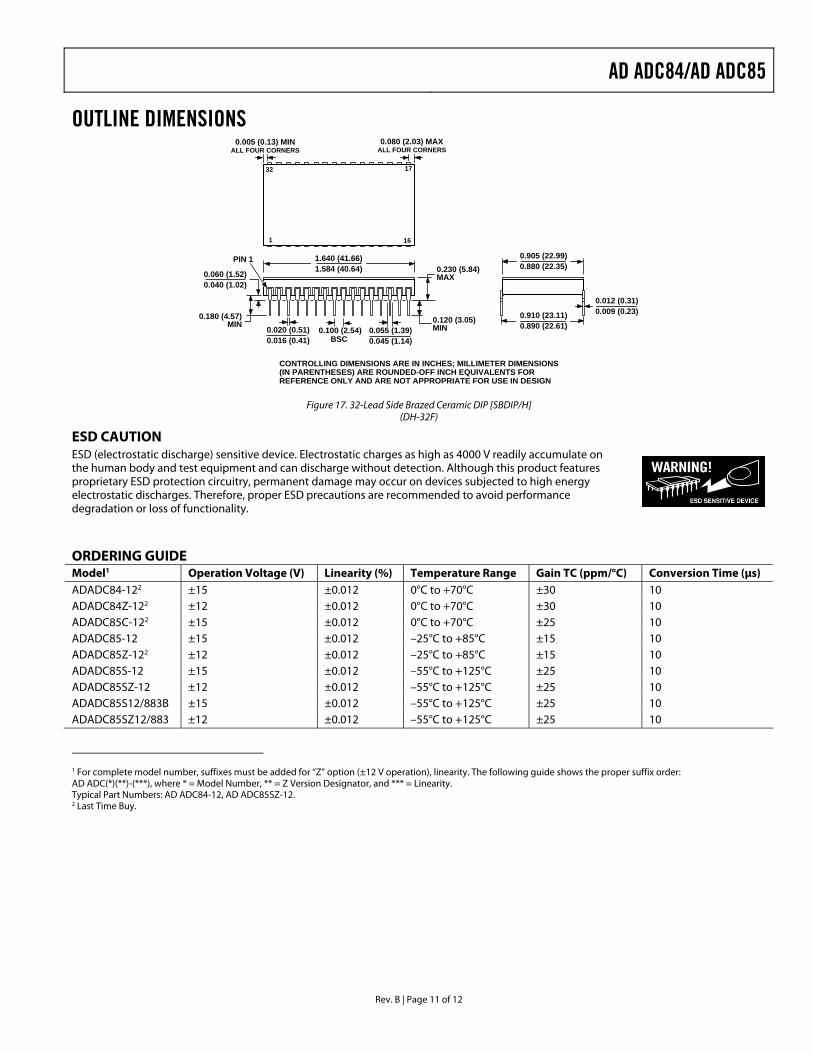
OUTLINE DIMENSIONS
0.120 (3.05)MIN0.020 (0.51)
0.016 (0.41)0.100 (2.54)
BSC
0.060 (1.52)0.040 (1.02)
0.910 (23.11)0.890 (22.61)
0.012 (0.31)0.009 (0.23)
1 16
1732
PIN 10.230 (5.84)MAX
1.640 (41.66)1.584 (40.64)
0.005 (0.13) MINALL FOUR CORNERS
0.905 (22.99)0.880 (22.35)
0.180 (4.57)MIN
0.055 (1.39)0.045 (1.14)
0.080 (2.03) MAXALL FOUR CORNERS
CONTROLLING DIMENSIONS ARE IN INCHES; MILLIMETER DIMENSIONS(IN PARENTHESES) ARE ROUNDED-OFF INCH EQUIVALENTS FORREFERENCE ONLY AND ARE NOT APPROPRIATE FOR USE IN DESIGN
Figure 17. 32-Lead Side Brazed Ceramic DIP [SBDIP/H] (DH-32F)
ESD CAUTION ESD (electrostatic discharge) sensitive device. Electrostatic charges as high as 4000 V readily accumulate on the human body and test equipment and can discharge without detection. Although this product features proprietary ESD protection circuitry, permanent damage may occur on devices subjected to high energy electrostatic discharges. Therefore, proper ESD precautions are recommended to avoid performance degradation or loss of functionality.
ORDERING GUIDE Model1 Operation Voltage (V) Linearity (%) Temperature Range Gain TC (ppm/°C) Conversion Time (µs) ADADC84-122 ±15 ±0.012 0°C to +70°C ±30 10 ADADC84Z-122 ±12 ±0.012 0°C to +70°C ±30 10 ADADC85C-122 ±15 ±0.012 0°C to +70°C ±25 10 ADADC85-12 ±15 ±0.012 –25°C to +85°C ±15 10 ADADC85Z-122 ±12 ±0.012 –25°C to +85°C ±15 10 ADADC85S-12 ±15 ±0.012 –55°C to +125°C ±25 10 ADADC85SZ-12 ±12 ±0.012 –55°C to +125°C ±25 10 ADADC85S12/883B ±15 ±0.012 –55°C to +125°C ±25 10 ADADC85SZ12/883 ±12 ±0.012 –55°C to +125°C ±25 10
1 For complete model number, suffixes must be added for “Z” option (±12 V operation), linearity. The following guide shows the proper suffix order: AD ADC(*)(**)-(***), where * = Model Number, ** = Z Version Designator, and *** = Linearity. Typical Part Numbers: AD ADC84-12, AD ADC85SZ-12. 2 Last Time Buy.

AD ADC84/AD ADC85
Rev. B | Page 12 of 12
NOTES
© 2003 Analog Devices, Inc. All rights reserved. Trademarks and registered trademarks are the property of their respective owners. C03262–0–11/03(B)