ad-a262 136 - dtic.mil · ad-a262 136 report of ... coates, doug usaf, wl/mtec cohen, eliot darpa...
TRANSCRIPT

AD-A262 136
REPORT OF
DEPARTMENT OF DEFENSE
ADVISORY GROUP ON ELECTRON DEVICES
APPENDIX TO
SPECIAL TECHNOLOGY AREA REVIEW
ON
MICROWAVE PACKAGING TECHNOLOGY
DTICELECTE
o'MAR 15190
FEBRUARY 1993 -
8 12 93-05335
OFFICE OF THE UNDER SECRETARY OF DEFENSE FOR ACQUISITION
WASHINGTON, D.C. 20301-3140

CLEARED
FOR OPEN PULCATION
FEB 10 1993 3DIRECTORATE FOR FREEDOM OF INFORMATION
AND SECURITY REVIEW OASO-:PA)DEPARTMENT OF DEFENSE
THIS REPORT IS A PRODUCT OF THE DEFENSE ADVISORY GROUPON ELECTRON DEVICES (AGED). THE AGED IS A FEDERAL ADVISORYCOMMITTEE ESTABLISHED TO PROVIDE INDEPENDENT ADVICE TOTHE OFFICE OF THE DIRECTOR OF DEFENSE RESEARCH ANDENGINEERING. STATEMENTS, OPINIONS, RECOMMENDATIONS, ANDCONCLUSIONS IN THIS REPORT DO NOT NECESSARILY REPRESENTTHE OFFICIAL POSITION OF THE DEPARTMENT OF DEFENSE

Table of Contents
PaRe1. MW Packaging Technology Workshop Agenda .............................. A I
2. MW Packaging Technology Workshop Attendance List ........................ A3
3. MW Packaging Technology Workshop Viewgraphs .......................... A7
4. Packaging Materials Information Tables* ................................ Al 14
5. Commercial Software for Packaging CAD/CAM ........................... A141
Aveepton For
NTIC -!?A&-i
DT.. .. . iD '; . T.F
* .... .....
* Included in this section is a listing of materials and their properties commonly used in MWand MMW MCMs. The information comes from the Raytheon-Texas Instruments MIMICPhase 2 Joint Venture and other Air Force sources.

- Al -
MICROWAVE PACKAGING TECHNOLOGY WORKSHOP
AGENDA18 June 1992
0730-0845 REGISTRATION/CONTINENTAL BREAKFAST
0845-0945 INTRODUCTION/DISCUSSION OF PACKAGING ISSUESTIM KEMERLEY, WRIGHT LABORATORY
0945-1030 MICROWAVE MULICIcIHIP MODULE PACKAGESRONALD NASTER, GENERAL El.ECTRIC
1030-1045 BREAK
1045-1130 MILLIMETER WAVE MULTIC1IIP MODULE PACKAGESBARRY ALLEN, TRW
1130-1215 MW/MMW PACKAGE DESIGN, MODELING & SIMULATIONPETER PARRISH, EESOF & ACHIM HILL, COMPACT SOFTWARE
1215-1330 LUNCH
1330-1415 PACKAGING MANUFACTURING TECHNOLOGYJOHN BEDINGER, TEXAS INSTRUMENTS
1415-1545 MILITARY vs COMMERCIAL PACKAGESJOHN TYLER, AVANTEK; RICK PERKO, M/A-COM;MICHAEL FLANDERS, COORS ELECTRONIC PACKAGE CO.
1545-1600 BREAK
1600-1800 PARALLEL SESSION WORKING GROUP DISCUSSIONS
1. MW MCM PACKAGES - CARL THOMAS, ROME LAB
2. MM WAVE MCM PACKAGES -KURT SHALKIIAUSER, NASA-LERC
3. MW/MMW PACKAGE DESIGN, MODELING &SIMULATION - BARRY PERLMAN, LABCOM ETDL
4. MILITARY vs COMMERCIAL PACKAGES -JOE COLUSSI, NAWC-ADWARM
ADJOURN

- A2 -
DRAFT AGENDA
19 June 1992
0730-0830 CONTINENTAL BREAKFAST
0830-1200 PARALLEL SESSION WORKING GROUP DISCUSSIONS -COMPLETE FINDINGS AND RECOMMENDATIONS -PREPARE SUMMARY PRESENTATION
1200-1315 LUNCH
1315-1600 EACH SESSION PRESENTS FINDINGS & RECOMMENDATIONSTO WORKSHOP PARTICIPANTS
ADJOURN

- A3 -
MICROWAVE PACKAGING TECHNOLOGY WORKSHOPGeorgia Institute of Technology
18-19 June 1992
ATTENDANCE LIST
NAME AFFILIATION
Adams, Richard W Ceramics Process Systems Corp.Allen, Barry R. TRW, Inc.Basine, James M. General Research Corp.Bedinger, John Texas InstrumentsBierig, Robert W AGED, WG/ABorkowski, Michael Raytheon Co.Brockett, William S. Martin MariettaBrodzinsky, Albert Vela Associates, Inc.Bugeau, John L. Lockheed Sanders, Inc.Burkett, Frank S. Jr. Hercules Defense ElectronicsCalcatera, Mark USAF, WL/ELMTCaldwell, Mike Scientific-AtlantaCaposell, Charles D. USN, NASCCoates, Doug USAF, WL/MTECCohen, Eliot DARPACollette, Susan MotorolaColussi, Joseph M. USN, NAWCCook, Arnold J. PCAST Equipment Co.Corbin, Victor Raytheon Co.Costello, John Westinghouse Electric Corp.Crouse, William A. TRW Space & DefenseDavern, William E. General Electric Co.Davidson, Tom USN, NSWCDecker, Richard Lehigh UniversityDickens, Larry Westinghouse Electric Corp.Dreyer, Gary Hughes Aircraft Co.Edwards, William J. USAF, WL/ELElwood, Persis A. USAF, WL/MTECEly, Kevin J. ITT - MECEnloe, Jack H. WR. GraceFelix, Joseph J. GEC - MarconiFitzhugh, Thomas E. Hughes Aircraft Co.Flanders, Michael Coors Electronic Package Co.Foster, Phil MIC TechnologyFullerton, Craig Motorola, Inc.

- A4 -
Microwave Packaging Technology WorkshopAttendance ListPage 2
Gamble, Richard A. USN, NCCOSCGelnovatch, Vladimir G. USA, SLCET-M, ETDLGoetz, Martin P. StratEdge Corp.Griffith, Gordon H. USAF, WL/MLPGupta, K.C. University of ColoradoHannon, Gregory E. Lanxide Electronic ComponentsHarris, Mike Georgia Institute of TechnologyHenry, Michael Paul USA, MICOMHerman, Martin Jet Propulsion LaboratoryHertling, David R. Georgia Institute of TechnologyHiggins, R.J. Georgia Institute of TechnologyHill, Achim Compact Softwareltoh, Tatsuo UCLAJohnson, Gerald E. Martin MariettaKagiwada, Reynold TRW, Inc.Katzenstein, West USN, NAWC-WPNSKehias, Lois T. USAF, WL/ELMDKemerley, Robert T USAF, WL/ELMKlug, James J. Harris Microwave SemiconductorKohl, Paul Georgia Institute of TechnologyKonsowski, Steve Westinghouse Electric Corp.Kopp, Bruce Johns Hopkins University, APLKoziarz, Walter A. USAF, RL/ERDRKruchek, Charles L. General Research Corp.Krumm, Charles F Hughes Aircraft Co.Lampen, James Raytheon Co.Landis, Richard C. Martin MariettaLaPalme, Richard HRB SystemsLee, Tim COMSATLewandowski, Bob USN, NASCU, Tom Martin MariettaUcciardello, Joseph A. Raytheon Co.Luce, Wyatt E. Westinghouse Electric Corp.McNulty, Mike GE AerospaceMacropoulos, Bill M/A-COM, Inc.Mah, Misoon Y USAF, WL/ELRDMandal, Robert P. Teledyne Monolithic MicrowaveMarchiando, Michael A USAF, WL/MTEMMartin, Pierre E. M/A-COM, Inc.Mason, James Texas InstrumentsMass, Steve TRW, Inc.

- A5 -
Microwave Packaging Technology WorkshopAttendance ListPage 3
Miller, Roger F GE AerospaceMisoni, John USN, NCCOSCNaster, Ronald J. General Electric Co.Nguyen, Richard USN, NCCOSC-NRADOrender, Robert J. USN, NSWCOwens, Joe Hughes Aircraft Co.Parrish, Peter T EEsof, Inc.Paul, Bralley J. USAF, WL/ELMTPeischl, Mark GEC MarconiPerko, Richard M/A-COM, Inc.Perman, Barry S. USA, SLCET-MPPeterson, Robert K. Texas InstrumentsReinhardt, John E. USA, MICOMRhein, James E. Raytheon Co.Robison, Dale L. USN, NAWCRomenesko, Bruce M. Johns Hopkins University, APLRoqueta, Elier C. ITT - MECRucker, Charles T Georgia Institute of TechnologyRussell, Kenneth J. The Aerospace Corp.Saloom, Joseph A. AGED, WG/ASandeau, Rene Martin MariettaShalkhauser, Kurt NASA/Lewis Research CenterShimoda, Raynor BoeingSobolewski, Lisa DARPAStaecker, Peter M/A-COM, Inc.Theim, Clare D. USAF, RL/ERSDThomas, Carl USAF, RL/OCTPTyler, John R. Avantek, Inc.Vorhaus, James L. Avantek, Inc.Wagner, Charles E. USAF, WL/MTECWeidner, Ken Coors Electronic Package Co.Wein, Deborah S. StratEdge Corp.Whicker, Lawrence R. Westinghouse Electric Corp.Young, Brian Hughes Aircraft Co.Ziegner, Bernhard A. M/A-COM, Inc.

- A6 -
S
a
a

- A7 -
MICROWAVE PACKAGINGTECHNOLOGY WORKSHOP
AGED WORKING GROUP A
18-19 JUNE 1992
ROBERT T. KEMERLEYWRIGHT LABORATORYWRIGHT-PATTERSON AFB)
MK 24
THE IMPORTANCE OFELECTRONICS PACKAGING
ELECTRONIC EQUIPMENT IS A DRIVER IN DoD SYSTEMS AND ASIGNIFICANT FACTOR iN THE US ECONOMY
AN INDIGENOUS INTERNATIONALLY COMPETITIVE ELECTRONICSINDUSTRY IS CRITICAL TO MAINTAINING A LEAD IN BOTH DEFENSEAND COMMERCIAL AREAS
FUTURE ELECTRONIC EQUIPMENTS REQUIRE LOW COST HIGHDENSITY MULTI-COMPONENT ASSEMBLIES (MCAs) AND ASSEMBLIESOF MCAs
ELECTRONIC PACKAGING IS IDENTIFIED AS AN AREA PROVIDINGOPPORTUNITY FOR SYSTEM PERFORMANCE ENHANCEMENT FORBOTH DEFENSE AND COMMERCIAL APPLICATIONS
M4 24 6

- AM -
STRATEGY FOR ELECTRONIC PACKAGING
INCREASE COORDINATION OF ELECTRONIC PACKAGINGINVESTMENTS WITHIN THE DoD AND OTHER GOVERNMENTAGENCIES
INCREASE DoD PARTICIPATION IN COOPERATIVE EFFORTSWITH THE INDUSTRY IN ELECTRONIC PACKAGING INCLUDINGR&D, STANDARDS, SPECIFICATIONS, TESTING, AND MANUFACTURING
WORK WITH THE ELECTRONICS INDUSTRY TO FORMULATE ACOORDINATED STRATEGY
A4 24 WO
MICROWAVE/MILLIMETER WAVE PACKAGING ISSUES
THE MOVE TO MICROWAVE/MILLIMETER WAVE MULTI-CHIPASSEMBLIES WITH HIGH DENSITY INTERCONNECTS IS CAUSINGA SIGNIFICANT SHIFT IN THE CURRENT PRACTICES OF HOWPACKAGES ARE BEING DESIGNED AND MANUFACTURED
THE LONGER TERM TREND IS TO MOVE TO SUBSYSTEM ORMULTI-LEVEL PACKAGING SCHEMES TO ACHIEVE HIGHERLEVELS OF SYSTEM INTEGRATION
PACKAGING COSTS ARE BEING EMPHASIZED EARLY IN SYSTEMDEVELOPMENTS
M-2A q

( MICROWAVE/MILLIMETER WAVE PACKAGING ISSUES
AREAS THAT REQUIRE DETAILED PLANNING AND INVESTMENT
- ADVANCED MATERIALS
- MULTI-LAYER SUBSTRATES
-HIGH DENSITY INTERCONNECTS
- DESIGN, MODELING, AND SIMULATION
- MANUFA(CTURING TECHNOLOGY
-SUBSYSTEM/MULTI-LEVEL PACKAGES
- TESTING AND CHARACTERIZATION
- PACKAGING DESIGN HANDBOOK AND STANDARDS
-QML
-RELIABILITY
- MILITARY -VS- COMMERCIAL TECHNOLOGY
M4 24 8
WORKSHOP GOALS
FOR DoD MICROWAVE/MILLIMETER WAVE MULTICHIP PACKAGINGAND INTERCONNECT TECHNOLOGY REQUIREMENTS
- DEFINE PACKAGING AND INTERCONNECT TECHNOLOGYAND MANUFACTURING PROBLEMS/ISSUES
- RECOMMEND SOLUTIONS TO THESE PROBLEMS BYDEVELOPING AN INVESTMENT STRATEGY THAT CANBE USED BY GOVERNMENT AND INDUSTRY
- BUILD UPON AND COUPLE TO THE 2-4 MAR 92 AGEDELECTRONICS PACKAGING TECHNOLOGY STA9
MA 2

- Alt0 -
WORKSHOP APPROACH
- IDENTIFY, PRIORITIZE AND RESOLVE ISSUES ASSOCIATEDWITH DoD MICROWAVE/MILLIMETER WAVE PACKAGING ANDINTERCONNECT TECHNOLOGIES
WORKSHOP AGENDA
"* SPECIAL INTEREST PRESENTATIONS
"• PARALLEL WORKING GROUPS
"• SUMMARY FEEDBACK SESSION
WORKSHOP FINDINGS AND RECOMMENDATIONSDOCUMENTED IN A REPORT
W424 3
FUNCTIONS OF WORKSHOP PARTICIPANTS
JOINT INDUSTRY/GOVERNMENT SESSION CHAIRMEN LEADINGDISCUSSIONS
INDUSTRIAL SPEAKERS
- SPECIAL FOCUS PRESENTATIONS
GOVERNMENT SESSION CHAIRMEN
- PROVIDE SUMMARY BRIEFINGS OF SESSION RESULTS
- PROVIDE 1-2 PAGE SUMMARIES OF SESSION RESULTS
WORKSHOP PARTICIPANTS
ACTIVELY PARTICIPATE IN SESSION DISCUSSIONS
PROVIDE INFORMATION ON ISSUES AND SOLUTIONS
FILL OUT ISSUE AND FEEDBACK WORKSHEETS
M4.24 4

- All -
PARALLEL WORKING SESSIONS
1. MICROWAVE MCM PACKAGES
2. MILLIMETER WAVE MCM PACKAGES
3. MICROWAVE/MILLIMETER WAVE PACKAGEDESIGN, MODELING AND SIMULATION
4. MILITARY -VS- COMMERCIAL PACKAGES
4 4 S45
ISSUE WORKSHEET
SESSION TITLE:
Issue Title:
Importance: _ Showstopper: - Needs to be done: - Nice idea:
Description of Issue:
Suggestion t I for Resolution of Issue:Resources Needed: - MYrs/Yr for __ Years
By this type of organization:
Suggestion # 2 for Resolution of Issue:Resources Needed: - MYrs/Yr for __ YearsBy this type of organization:
Suggestion a 3 for Resolution of Issuc:Resources Needed: _ MYrs/Yr for _ YearsBy this type of organization:

- A12 -
FEEDBACK FOR SESSION
The sessions are large and ume is short. This is your mechanism to endorse or object tothe findings and recommendations. It is very important that you complete this feedbackform. They will be analyzed to develop a sense of priority of the findings andrecommendations. It is also important that you ci•ce all of the following desctptors thatchaacterizC where you are 'coming from*. SUPPLIER USER GOVERNMENTINDUSTRY ACADEMIA COOPERATIVE CONSULTANT ENGINEERMARKETING MANAGEMENT MATERIALS COMPONENTS SUBASSEMBLYSYSTEM
Optional Informaton: Name: Affiliation:
Issue Title:Suggestion # -
Circle: Strongly Agree 10 8 6 4 2 Strongly Disaree
Comments that you want reflected in the rinal report on the issue.
Issue Title:
Suggestion *
Circle: Strongly Agree 10 8 b 4 2 Strongly Disagree
Comments that you want reflected in the final report on the issue:
Issue Title:
Suggestion #
Circle: Strongly Agree 10 8 6 4 2 Strongly Disagree
Comments that you want reflected in the final report on the issue:
DoD AGED WORKING GROUP A ACKNOWLEDGES
GEORGIA INSTITUTE OF TECHNOLOGY, MR C.T. RUCKER
PALISADES INSTITUTE FOR RESEARCH SERVICES, MS P. MYERS
FOR THEIR SUPPORT IN ORGANIZING THE MICROWAVE PACKAGINGTECHNOLOGY WORKSHOP

- A13 -
Microwave MultichipModule Packaging
GE Aerospace
Microwave Packaging Technology WorkshopGeorgia Institute of Technology
Ron NasterGE - Electronics LaboratorySyracuse, New York(315) 456-2046
RJN 6112'92 39
Microwave Multichip Module Package - OutlineGE Aerospace
* Microwave Packaging Requirements
"* Packaging Concepts and Assemblies
* Materials and Housing
"* Interconnects
"* Advanced Systems and Technology
* Development Needs

- A14 -fi 6,12!3
Present Microwave Packaging Requirements - 1992 GE Aerospce
Reliable Enclosure
- Hermetic enclosure requires leak rate less than 5 x 10⁻⁸ atm-cc/secfor active components.
- High thermal conductivity required to dissipate high power fromconfined areas.
- Materials must match CTE of GaAs and Silicon.
* Highly Reproducible Performance
- Required to maintain channel phase and amplitude tracking.
- Places light tolerance on line width and dielectric thickness dimensions
* Low Cost
- Required to meet budgets for large arrays
- Must be consistent with tight tolerances and use of high performancematerials.
- Forces designs which are compatible with batch processing andautomated assembly and test.
RJN 6/12t92-4
Present Microwave Packaging Requirements - 1992 GE Aerospace
- Weight and Size- Must fit within phased array antenna grid spacing and stay within platform weight budget.
- Mode Suppression- Package geometry must be designed to avoid circuit-to-package coupling to eliminate
package induced performance anamolies and waveguide modes.
* Interconnect
- Low Loss is required to achieve high efficiency, high transmit power and low noise figure.
- Well controlled 50 ohm impedance is required for power transfer.
- Greater than 60 dB isolation is required between microwave interconnects and betweenmicrowave interconnects and control and power supply lines.
- Feedthroughs- Low resistance DC feedthroughs are required for high current distribution.- Low loss 50 ohm microwave feedthroughs

- A15 -
11 IN Iii 12r 9` 4j
Microwave Packaging - Drivers GE Aerospace
SYSTEM REQUIREMENTS - Stressing performance specificationsimpose severe requirements on package heat sinking, loss, andconsistency.- High transmit power- Low receiver noise figure- Module-to-module tracking
DISTRIBUTED SYSTEMS - Trend to decentralize and distribute supportelectronics at antenna forces microwave/digital integration.- Distributed signal control functions- Distributed power conditioning- Intra-module calibration- Distributed beamsteering computation logic- Digital beamforming
DIVERSE COMPONENT INTEGRATION - Module performance is best achievedthrough integration of dissimilar microwave/digital technology.- Microwave: GaAs (MESFET, HEMT, HBT), InP, Si, and SiC, Diamond- Digital: GaAs, Si- Power conditioning: Si- Optical: GaAs
HIGH DENSITY PACKAGING - High packing density is required to integrateelectronics in antenna grid spacing and meet system size and weightrequirements.
HEAT SINKING - Increased module performance and functionality increases heat sinking
required for reliable operation.
High density packaging is required to integrate diversecomponent technology into future systems.
RJN 6&I2J92-35
Power Dissipation/Antenna AreaGE Aerospace
Freq. P0 (Peak) I PDis PDis/Area(GHz) (Watts) (%) (Watts) (Watt/in 2 )
1 200-400 50 40-80 1.2-2.4
3 50-100 45 12-24 3.2-6.4
10 12-24 40 3.6-7.2 11-22
30 2-4 30 .9-1.9 24-48
100 .2-.4 15 .22-.45 63-126
Duty Factor = 20%

- A16 -
Phased Array Dissipated Power GE Aerospace
100
60
40 .. .. .
W atts/In. 2 20 . ./
10 20. 0400.1 20 345 0
10
8.0
4.0
10 20 30 40 50 10 20 30 40 So IGO
Frequency (GHz)
RJN 6/12/92-42
TIR Module Architecture GE Aerospace
PowerMicrowave
S~PHEMT/HBT.. _/ .. Silicon Bipolar /
Optical Opto-electronic
Transducer
/ LNA
Digital
GaAs FETSi/GaO GaAs GaAs FET GaAs PHEMT GaAs PIN
Si PIN
Control IPower
C Conditioning
GaAs FET Silicon BipolarSilicon CMOD

- A17 -
RJN 6i 12'92 V
Semiconductor Properties (Room Temperature) GE Aerospace
k CTE E P r
Material Thermal Coef of Dens DielResistivityC T r Modulus Resistivity Constant TangentW/n- pmC Lb/in*J 106 pi pil-cmCo d Therm. p bi psi at Microwave Frequencies
Gallium Arsenide 1.0 5.8 .19 124 8.1 12.8 0016Indium Phosphide 1.8 4.6 .17 - - 12.3 -Silicon 3.4 3.2 .084 15.5 850. 11.0 .001-01Silicon Carbide 6.8 3.7 .116 48 1 - - -Diamond, Type 2A 50 .8 .127 -- .102 6 5 7Germanium 1.5 5.8 .19 11.4 45. 15 7
FUJN 6,12 b
Ceramic/Glass Properties - Room Temperature GE Aerospace
k CTE E ErThermal Coef of 7 Elastic P Dielectric LossCond. Therm. Exp. Dens Md6 Resistivity Constant TangentWfin-C ppm/C Lbnint 106 psi pQ-cm at Microwave Frequencies
Air .00066 .000042 1.0Alumina
99% .93 6.7 .W41 55 >1020 9.9 .000196% .89 6.4 .141 47 >1019 9.2 000394% .70 6.0 .141 43 >1019 8.8 .001
Alumina Nitride 2.5-4.3 4.1 .116 40 >1019 8.8 .001Barium Titanate .19 9.5 .200 >1018 38 .0002Beryllia 99.5% 6.3 6.7 .105 48.5 >1021 6.7 004Sapphire 1.2 5.6 .144 55 >1021 11.0 .001-.002Silic (fused) .04 .6 .079 10.6 >1017 3.8 0012Glass (variable) .025 .092 8.7 >1022 5-6 .0027059 (BaBoSillcate 4.6 9.8 >1014 4.8 .0057070 3,2 .077 7.4 4.1 .00257740 3.3 081 9.1 46 026Quartz .04 .6 .079 12.5 3.8 0001

- A18 -
Packaging Material Properties - Metals GE Aerospace
k CTE E Fr 6Material Thermal Coef of Elastic P Dielectric LossCond. Therm. Exp. Densit Modulus Resistivity Constant Tangent
Wfin-C ppmrC Lb/in7 106 psi pi1-cm at Microwave Frequencies
Copper, pure forms 9.9 16.8 .323 17.6 1,72
Gold 7.5 14.2 .698 11.5 2.4
Aluminum, 1000 5.7 23.4 .097 to 2.66000 4-9 23.4 .097 10 2.6
2000, 3000,5000 4.6 23.4 .097 10 2.6
7000 3.1 23.4 .097 10 2,6
Molybdenum 36 49 369 478 48
Brass 12-5.2 185 .308 16 5 3.9
Beryllium 3.9 11 5 .067 42 4-6
Nickel 1.9 13.3 .322 30 6 9
Kovar .45 4.9 .302 19 45-85
Invar .28 1,6 ,290 20.5
C/I/C (12.5/75/12.5) 3.1(x-y) 190(Cu/Invar/Cu) 4.2(z)
(16/68116) 4 2(x-y) 19.05.4(z)
(20/60120) 5.5(x-y) 19.06.7(z)
Silver 10.6 19.6 .379 11.6 1.62
Die Attach Properties (Room Temperature) GE Aerospace
k CTE E ErMaterial Thermal Coet of I Elastic P Dielectric Loss
Cond. Therm. Exp. Modulus Resistivity Constant TangentW/In-C ppm/C Win 106 psi AO-cm at Microwave Frequencies
Gold/TIn (80/20) V.4 15.9 .542 8.6
TInLead (63/67) 1.3 24.7 .305 4 15.0
(60/40) 1.3 23.9 .308 15.0
(50/50) 1.3 24.8 .321 15.6
(40/60) 1.1 - 24.6 .335 17.0
(30/70) .351 18.5
(20/80) .95 26.5 .368 19.8
(10/90) .91 .389
SrnAg (96.513.5) .375 12,3
Sn/Pb/Ag (62/36/2) 1.3 27 .307 3.3
Indium 2.0 32.7 .264 1.6 9.0
Epoxy, Able 826-1 .053 32 .087 .2 300
Able 84-1 LMI .048 55

- A19 -
11 jj F, l1' 9? 7
Composite Electronic Packaging GE Aerospace
Composites Advantages"• High thermal conductivity• Tailorable CTE"* Low density"* Low cost in high volume applications"• Weight savings to 80%"* Net shape fabrication
Key Materials"* Silicon carbide particle/aluminum"• Diamond particle/aluminum"• Carbon fiber/aluminum" Carbon fiber/copper"* Carbon fiber/epoxy - aluminum laminate"• Carbon fiber/epoxy - copper laminate
PjN 0112,1' 1
Reinforcements GE Aerospace
Discontinuous Fibers,Continuous Fibers Whiskers
Reinforcement
Matrix Metal Ceramic Poylmer
Metal X X XCeramic X X X
Particles Fabric, Braid, Etc. Poylmer X X X

- A20 -J C
Metal Matrix Composite Properties (Room Temperature) GE Aerospace
k CTE E ErMaterial Thermal Coef of D Elastic Dielectric LossM lCond. Therm. Exp Den!Y Modulus Resistivity Constant Tangent
W/in-C ppm/C Win 106 psi pi-cm at Microwave Frequencies
PIOOGr (20%)II100A 5.5 (x-y) 10.3 (x-y) .093 18 (x-y)
3.8 (z) 27 (z) 6.8 (z)
(25%)/ 5.5 (x-y) 8.3 (x-y) ,091 20 (x-y)
3.5 (z) 27 (z) 6.0 (z)
(30%)/ 5.5 (x-y) 6.7 (x-y) .090 22 (x-y)
3.1 (z) 27 (z) 5.4 (z)
(40%)I 5.5 (x-y) .086 26 (x-y)
2.1 (z) 42 7)
(50%)/ 5.7 (x-y) .083 30 (x-y)
2.0 (z) 3.2 (z)
P75Gr(10%)I1100AI 5.1(x-y) 17.3 (x-y) .097 12.5 (x-y)
(20%)/ 4.6 (x-y) 12.6 (x-y) .093 15.1 (x-y)
27 (z) 6.8 (x-z)
(30%)/ 4.1 (x-y) 8.9 (x-y) .090 17.7 (x-y)
27 (z) 5.4 (z)
SIC (40%YAI 2.5 12.6 .105 21
(60%)/ 4.06 7.0 .10 26.1
(70%)/ 4.06 6.2 .10 26.1
CM-15 4.7 7.0 .36
CW-10 5.3 6.5 .61 -
CW-15 5.7 7.0 .59 -
CW ,20 6.3 8.5 .57 --
RJN 6112/92.10
Fiber-Reinforced MMCs GE Aerospace
Advantages- Very low CTEs possible- Very high conductivities possible (>copper)- Low density- Easily machined (some)
Disadvantages- High cost
Limited shape capability (e.g., plates)- Hard to machine (some)- Hysteresis. Galvanic corrosion for C/Al- Poor transverse strength for C/Al, C/Cu
* Key matrix materials: Aluminum, Copper
e Key fibers; graphite (carbon), boron, silicon carbide

- A21 -
iJN b, I ? ý
Particle-Reinforced MMCs - Key Materials GE Aerospace
* Aluminum reinforced with- Silicon Carbide - (SIC)p/AI- Diamond - (Diamond)p/AI (experimental)- Aluminum Nitride - (AIN)p/AI (experimental)
- Beryllia-reinforced Beryllium-(BeO)p/Be
* Diamond/Magnesium - (Diamond)p/AI (experimental)
* Many other systems possible- e.g., copper matrix
Gr-AI Cyclic Thermal Expansion - 3 Cycles GE Aerospace
4. BE-4
3. SE-4
CS 2.E Q•-4
C
1 ..SE-4
-SUB -IS-O88 8 266 569
TEMPERATURE (F)

- A22 -
Tungsten/Copper Cyclic Thermal Expansion - 4 Cycles GE Aerospace
o wigz0l
a WIG
4 W014 .0
INOIZ
SWI
, - ISt Cycle CTE = 6.9 pprr'cC
2 nd Cycle CTE = 6,8 ppmIVC* - 3rd Cycle CTE 6.9 ppm/°C
I
-I BIOd
- W02 4F 8 2 1 29W 240
TE"ERAATURE (C)
SiC(p)/Alumina Cyclic Thermal Expansion - 3 Cycles GE Aeosop.ce
I WN
I MIG
-1
TEM4PERA1URE (tf)

- A23 -
CTE of Electronic Materials GE Aerospace
25At
20
SlCp/AI C/At
Cu
15 Glass/
CTE (10-6 /KI 10 B.O/ .-B. C/•GaAs -
A12 0 3 0
Botoollicale MGMJGlass 0 Silicon
Quartz 0
0
C/Ep
-5 I 10 200 400 600 800
heteimal Conductivily IW/mK]
METAL MATRIX COMPOSITE AND "KOVAR"MICROWAVE PACKAGES
GE Aerospace
OUR CJIV METAL PD MRIUG COPST
IT - 42 - -°5 "
THEIML . 9.6 STUl TIIL 74 B1UCONDUCTIJVITi ItIR-1-•F COIDUJCIV Ily HRIM-F

Kovar and Metal Matric Composite Package Costs GE Aerospace
$2000~
.0E
,~$1500 '
U)
0oa
$5000
0 1000 2000 3000 4000 5000Quantity
Materials & Structures
High-Thermal-Conductivity Mullichip Module GEAmp-
GR/CU
*P120 carbon fiber/copper base*Tailored CTE matches alumina*Advantages vs. miolybdenum
3 x thermal conductivity25% lighter

- A25 -
Equipment Division RaytheonAMICDO Pressure Infiltration Casting
"* Form of liquid infiltration utilizing pressurized inert gas to force molten metalinto a preform of reinforcement material
"• Allows for inexpensive production of net-shaped composite materials withtailorable properties
"* Pressure infiltration utilizes controlled pressurization - high infiltration pressureswith low differential pressures inside and outside of mold
- Reduces sealing problems- Lowers required wall strength- Minimizes thermal mass of molds- Lowers tooling costs
"• Key characteristic - process does not rely on matrix wetting by the moltenmetal and is capable of high melt temperatures; therefore, many combinationsof reinforcement and matrix alloys are possible
Aluminum silicon carbideGraphite aluminumDiamond goldGraphite copper
N"

- A26 -
IiN 61121"j?.
Equipment Division RaytheonAMICDO Powder Injection Molding
"* Form of powdered metallurgy where net shape formation of potentiallyinexpensive composite metal housings is possible
"* Powder Injection Molding Process- Selected metals are milled to fine, uniform particle sizes- Fine metal powder is mixed with organic binders for adhesion- Pliable mixture is injection molded to shape- Shaped part is sintered in hydrogen furnace at very high temperatures. Multiple furnace firing occurs until the binders are removed and part
density is achieved
"* Process design characteristics include- Control of metal powder size to prevent agglomeration of metal particles
during sintering- Control of heating rate during sintering to minimize shrinkage and warpage- Mold design to accommodate 20% shrinkage of part during firing
Conclusions
0 Low Cost (- $50) TUR Module Package Is Achievable In Large Quantities
* Metal Injection Molded Package Is Lowest Cost Solution ior Packages WithFeatures Like Septums, Grooves etc.
* Ring and Base Package Appears to Be Lowest Cost for FeaturelessEnclosures
* AISIC Pressure Cast Packages Offer Minimum Weight at 10% - 20% HigherCost (5 $50)

-A27-
LTCC/HTCC Comparison GE Aerospace
LTCC Thick Film on HTCCPackage 96% Alumina (92%," Alumina)
Physical PropertiesGTE at 300CC (ppmrC) 7.9 6 4 6Density (g/cm3) 2.9 3 7 '3 6Camber (mils/inch) 1-4 1 -2 1 -.1Surface smoothness (microinches) 8.7 14.5 2,' ))Thermal conductivity (W/m K) 16-20 20 141-18Flexural strength (kpsi) 22 40()1Thickness/layer after firing (mils) 3,5-10.0 0.5-1,( -520
Dimensional Shrinkage TolerancesLength and width ± 0-20% NiA1Thickness ± 0.5%; N/A -.5 0%.
Electrical PropertiesInsulation resistance (ohms at 100 VOC) > 1012 > 1012 >i)1&2Breakdown field (volts/mul) > 1,000 > 1 .000 -~700
Dielectric constant (1 MHz) 7.1 9 3 8 9Dissipation factor (%) 0.3 0 3 U 03Buried conductor res. (mu/I o) 5.0 - 1)00Microstrip loss (dB/in @ 10 GHz) 0.83 - )
Integrated res. & cap. Yes
MIMIC Multi-Chip LTCC Package
f~L HAR~IS A6 CAC NK7EH EEoI rip E-SYSTEMS j AT&T hf4COM1
Basic ConstructionCavitiesTop FilmResistors
-< SignalLayers
Thermal PowerVia' Plane
~- Ground
Advantages*Integration of Transmission Structures*Complete Hermetic Package*Compact Size for Complex Circuitry Single channel X-Band LTCC Module*Low Cast in High Volume 1NOVO)D6C0519 ,

-A28-
LTCC PACKAGING FORMIMIC X-BAND RADAR MODULE
•3 HARRIS A cMAse movto E•E,. CaEE-SYSTEMS • AT&T AYCC41
FEATURES
. 15 3.5 mil CIRCUIT LAYERS
- 10 10 mil SEAL RING LAYERS
• 4 MICROSTRIP TO STRIPLINE TRANSITIONS
*,2 ISOLATED AND SHIELDED STRIPLINES
- -4 THERMAL ELECTRICAL GROUND VIA FIELDS
. ISOLATION AND MODE SUPPRESSION VIAS"THROUGH ALL 15 LAYERS
• GROUND PLANES IN ALL LAYERS
. EMI SHIELDING IN SEAL RING SIDEWALLS
. SHRINKAGE CONTROL ±0.2%
* LOSS AS LOW AS 0.2 dB/INCH(AX203= 0.2dB/INCH)

- A29 -
MPAUT microwave Packaging andl interconnectTechnology for Phased Arrays (WL) GE Aerospace
(D I E n Semiconductor-based processes and equipmentHol MUttliarr , Denser packaging which increases batch size
t' Host *Improved module yield through adaptive lithography
TechnologyDevelopment
~~I ' ~-Interconnect-~ * RF-~ transmission
media*Wafer-levelfabrication
Size: 0.55"x1.5"x0.06"U ColnWeight reauced to Hrmtcsa
Microwave HDI results in significant reduction in module size,weight, and cost
'Ttbak&Sqm tot pmne4 At~C"MsqA ~3 510 1,?43
WO~ ft..iSU14y SSfo 1f04 W.Ift
*~Suba i.ed by:
2104f P.Otmono. AFS ON .u,..M

- A30 -
Key MPIT Program Elements
Reauirement Westlnohouse Approach Benefits
Low Cost Batch ProcessingHost Water Selection High Resistivity Silicon Commercially Available
Fine Line Geometriee
Processing of RF/DC Precision Thin Rim Batch ProceseingInlerconnects & Passive on Si motherstrete Reduced Parts CountComponents
Reduced Stress Dle AttachGaAs/Si Component with Metal Shims Batch ProcessingAttach & Interconnects TRW Cmplmant RIterconnect Enhanced Reliability
WEC Auto- Wirebonding
Single Layer, High OensltyRF Transmhlslon Media MIcrostrip Supports Multiple Interconnect
Processes
Wafer Level Test RF Wafer Probing Fully AutomatedAutomated Module Test Improved Yield, Low Cost
Thermal Management Thermal Spreaders Improved ReliabilityFilled Thermal Visa Integrated Approach
Hermetic Coatings WECilndustry Initiatives Reduced Cost & WeightOrganic/inorganic Coatings
N*CROWAVEPACKAGI&G ,WTERCDYECT TECtROLOGY.
MPAIT Development Plan GE Aerospace
"* Host Wafer - AIN used for high thermal conductivity and excellent mechanical properties.Thermal expansion coefficient is matched to GaAs by copper deposition.
"• DC/RF Interconnect - Thin film metallization on Kapton defined by laser lithography allows lace-up dieattach.
"* Die Attach & - Process compatible with standard eutectic, epoxy, and thermoplastic resins.Interconnect - MMICs fill 80% of module area
- 3:1 module size reduction
"* RF Transmission - High density thin film microstrip interconnect compatible with MMICs increases RFMedia density by 10:1
- Microslnp lines are adaptively adjusted for MMIC misalignment- Shielded RF crossovers- RF feedthroughs buried in cotitred AIN- Low ohmic and mismatch loss
"* Water-Level - TIR modules fabricated on 6 inch wafersCharacterization, - Standard cassette-to-casselte handlingDicing, and Test - RF autoprobing at wafer level
"* Cooling - Face-up bonding and 4-mil MMICs provide best thermal path- Conventional cooling possible to 4 watts- Microchannel cooling in or external to host wafer allows output power to increase to
15 watts
"• Hermetic Seal - Integral hermetic package without wails- Near term batch processed metal cover- Longer lerm uses thin film conformal coaling

-A31 -
0 PICKAND PLACE AUTOMATION DEVELOPMENT
REDUCES VARIATION AND LOWERS COST
DEM/VAL MANTECH PHASE 2 4400 MODULE
* 124 COMPONENTS/MODULE 0 41 COMPONENTSIMODULE 0 17 COMPOt4ENTS/MOOILE* 5 SUBASSEMBLIES 0 3 SU13ASSEMBLIES 0 NO SUBASSEMB3LIES
INTEG RATED- - AUTOWORK CELL
* SEMI-AUTOMATIC PROCESS 0 FULLY AUTOMATIC PROCESS 0 INTEGRATED MFG PROCESS0*/.-,007 INCH/LIMITED FEEDERS Is +/.003 INCHiMULTI-FEEDERS 0 */.-.0005 INCH/MULTI-FEEDERS0 70 - 95% YIELD (COMP) 0 99.9% YIELD (1000 ppm) 0 99.99%. YIELD (100 ppmI)
0 10 MODULESISHIFTIMACHINE 0 78 MOOU LESiSHIFT/MAC HINE * 200 MQDULESiSHIFTIMACHINE
0 340,MeDULE (PL:US REplq 01MO2'E(1I~f~WORK) a 6SMI'MODip- Snr LL INC 8FWQRK1@1000 MODULESDAY
Wirebond Ultrasonic Signal Analysis."K , da"
Cuffrent Envelcpe- Time Record of V/S Pulse- Rise Time, Duration- Basis for Frequency Response
Frequency Response-Curr ent- Fourier Transform of Current Envelops- Mechmnical Resonant Frequency- Shape, Magnitude Relate to Bond Quality
- Frequency Response - Impedance
-voltage (CurrentDepends on Bond Geometry
-Relates Directly to Bond Quality
Ultrasonic Monitors for Wirebonding
- esueetsRlte t Bnd Qualtyumnt1StrengthViueManlc JitVa

- A32 -
Silicon Wafer Processing Provides theTechnology to Batch Process T/R Modules
• Flip Chip
~2nd Metal
Polyimide
Via1 st Metal
4 Watt Transmit Module WillDemonstrate Feasibility of Wafer
Fabrication of T/R Modules
-.. SiN, and2 Wax Conlor--,i (,a
Etched Polyimide With dc and L oq•ic LineS
AIN Substrale With LMW afd ,as Loies. Winh Ilip (JOp Iir
AJN Cold Plate With I jqud Mi;cochannels
AIN Coolanl Disirbulon Maiiloid

- A13. ---Designing for Manufacturing YieldDie Yield After Attachment and Number of Die
Per Hybrid Will Determine the Hybrid Yield
90 93.9% Mie cssembly Yield
so f-
701 99•lei-
20
0 5 10 15 20 25 30 35 40 45 ~Number ot Die/Hlybrid
Four Areas to Address to Achieve Desired Hybrid Yield:
1. Partitioning, to Reduce the Number of Die Per Hybrid2. Die Test, to Start With a Higher Percentage of Good Die3. Assembly Improvements, Design for High Assembly Yields4. Rework, Initial Design Must Allow Cost Effective Rework
§,.:1'z492-OI •.4 "
S-T_
-r 1-A Transmit
Clad" Module Has",,_. .Already Been
Designed/- " "for MCM
Manufacturing
IaP

- A34 -RJN 6/12,92-5
Future Microwave Packaging Requirements - 2000 GE Aerospace
" High Density Integration- High Density Integration of microwave and digital electronics to increase radar
performance through improved calibration, adaptive nulling, digital beam forming,distributed signal processing, etc.
"* Improved Heat Removal- Additional heat removal capacity to handle thermal load of higher power transmitters andincreased module integration.
"* Opto-electronics Integration- Integration of opto-electronic components for mating with fiber optic beamformer and
control harnesses.
"* Multi-layer Packaging- Multi-layer packaging for increased volume integration and insertion into thin
conformal array structures.
RJN 6&492-6
Phased Array Thrust GE Aerospace
1980 1990 2000
IF~~ n H ~ L DCneson R
Drivr ~Beam steowing Clii Pwr CondI V l Flo I.E..*e,
RF & Digitla Beam Steering CiOi Pwr CondI Oi Lotic Pw Cord o, _0,I n. : ,n
rierI W#CoBeam Steeknn C~t ; Pr Cod
* Phase & Gain Control* Transmitter (GaAs)
* Phase & Gain Conirol (GaAs) , Receiver (GaAs)
Elemental PTransmitter (GaAs) Conirol Logic (GaAs)
Electronics Phase Control (Silicon) * Receiver (GaAs) * Power Con•itioning (Slicon)
* Control Logic (GaAs) Beam Steering (Silicon)* Power Conditioning (Silicon) , Performance Monitonring
SCalibration* Space Time Adaptive Processing
D Digital Beamlormng* Signal Processing
* Transmitter (Tube/Silicon)* Receiver (GaAs) * Beam Steering (Silicon)
Centralized * Power Concitioning * Performance MonoringElectronics * Beam Steering Computer * Calibration Data Processig
* Performance Monitoring * Adaptive Nulling Display* Calitxation SignaLiData Processing* SigilDOata Processing Display• Display

Conformal Airborne Arrays - A35 - G eopc
,Airborne integration places extraordinary demandson packaging, interconnects, thermal control, andmechanical structure.
2000 Tactics,
of DOWtrBUteOWOd Proceso
and ~C add newperormncecapbilty
"Microwavue/dgia P negatdPakainsEserspc
"Coc RategaeAcie'o
FoDutr irone radar, adilicod ankain aandphtnTheholg irdckes raa 4 egh mans cothikes25mlanddnwoefomnce Planeabiality. n 'ueci/px Atcmn
MuisrateavCe/machgit als Intgrte matchawinh Si DvopcmAtberospbtae/
(5ue.8 p Micrwav (3.2 ta Np~ dei essemdo as /S
Average 'OT Power 3 5-5 6.7s220Wat
tnterconn *th'ioknlss tra4smilsinle *~Highdensit Hig d20i25g isoltioSystem 'LGowunductane MeaFligrtouing Lo s tcritossal Attitachntrcnnctntte
SoHigh oEpower tahmn
'Effraeicien heatc removGals *CEiin heatc removalHighDtherma comdpatibvsbtrat/C
Packaging3 W/inOee pakgn 4.r tight -Macemetal matrix pSi ackge
antennalupe element grdsatching

RNk; 92 2u
- A36 -
Microchannel Cooling Effect on Tj(max) and P0 GE Aerospace
Singl acool ngChi innel t7(Bas line Dsign) Mcrocha l
:'15o.& 4 W tt bi
%140 MdlC
C
E 120 - - - osiLwaf uI
2 ___gr rwtht 44 W Itt maoiuie
0 2 4 6 8 10 12 14 16 18 201 Output Power (W)
Transmit power can be reliably increased to 44 watts withAIN and microchannel cooling.
RJN 6112192-19
Fiber-Optic Microwave/Optical Interface GE Aerospace
Monitor Laser Sphwical Optical GRINDetector Diode Lens Isolator Lens
DLavseAr D pticalo i
Detector Matching NetworkRF in RIFout

- A37 -
Microwave Packaging - Summary GE Aerospace
" Improved packaging and interconnect systems are requiredPackaging material compatibility with GaAs and silicon
a Thermal coefficient of expansiono High thermal conductivity
Higher Density Interconnects" Uncompromised microwave performance• High isolation for reduced microwave/digital coupling (crosstalk)"* Top level *flying lead' replacement
Feedthrough Connections"• Low microwave loss"• High power DC"* High density control
Low-Cost"• Materials"• Automated assembly and test* Wirebond replacement
"* Advanced Technology needed Ior future higher powerihighlyintegrated systems
"* Multilevel packaging"* Lightweight/low cost metal matrix materials* Optical component insertion for microwave and high speeddigital interconnects

- A38 -
Millimeter-Wave Multi-Chip Module Packages
Barry R. Allen
Microwave Packaging Technology WorkshopAtlanta, GeorgiaJune 18, 1992
Millimeter Wave Packaging Topics
"° Requirements
"* Challenges
"* Examples
"* Comments and conclusions

- A39 -
Millimeter-Wave Packaging Requirements Trw
0 Extension of microwave requirements
* Unique challenges
- external RF interfaces less standardized- dimensional tolerances decrease with frequency- dielectric based packages exhibit many resonance modes- conductor losses increase rapidly, (L - fP' for optimum single-mode line)
arrays require dense RF, DC and control packing
* And opportunities
- passive components smaller for higher level of integration in package- integrated package and antenna more practical- dielectric interconnccts possible in some cases- quasi-optical systems for improved performance
Millimeter-Wave Packaging Requirements
Package Function Millimeter Wave Requirement
External RF interfaces Low loss, low VSWRLow unwanted radiation
Internal RF ii 1,erfaces Repeatable chip-to-chip connections
Internal signal distribution Low loss, low VSWRLow unwanted coupling
Internal and external signal isolation High isolation, no mode coupling
DC/Control distribution No RF degradation
Hermeticity Required at present
Thermal management Minimize temperature rise for reliability
Low cost Required in relatively low volume
Small size Key requirement in arrays
Light weight Required in arrays and munitions

- A40 -
Millimeter-Wave Packaging Challenges TRW
Package Function Millimeter Wave Challenge
External RIF interfaces Likely to be waveguide or antennaFew standards
Internal RF interfaces Radiation and repeatability
Internal signal distribution Microstrip or stripline plus othersInternal and external signal isolation Isolation difficult in non-metallic package
DC/Control distribution Constricted space
Hermeticity Usually adds significant lossThermal management Higher power density for transmit
Low cost Difficult with prec;sion dimensions
Small size All dimensions not scaled equally
Light weight Limited by thermal requirements
Millimeter-Wave Packaging ChallengesA
"• Millimeter wave MMICs relatively new technology
"• Usually machined metal housings and single layer substrates at present
"* Present fabrication limits restrict multi-layer substrates to about 40 GHz
"* DoD (and eventual commercial) needs require lower cost packaging
"° Millimeter packaging for low cost requires:
- Accurate CAD for EM, thermal, and mechanical simulation
- Improved, repeatable mechanical and electrical properties
- Reliable, available package suppliers

- A41 -
Millimeter-Wave Packaging Approach
"* Most packaging approaches use four main elements:
1 - Package base2 - Package walls3 - Internal Interconnects4 - Package interface
"* Each major package element is somewhat independent, resulting a number ofconfigurations.
"* The lowest cost packaging approaches provide batch or automated processingof all package elements.
Millimeter-Wave Packaging Electrical Limits T#uww
Approximate dimensional limits for mode-free multilayer alumina microstrip(e, = 9.9)
Maximum Maximum MaximumFrequency Spacing Substrate(GHz) Via Thickness Feedthrough(mils) (mils) Diameter
10 170 50 150
30 57 17 50
60 28 8 25
90 19 6 17
120 14 4 131Dimensions scale approximately as-

A42 -
Millimeter-Wave Package Base°
Implementation Characteristics
- Excellent shielding and groundingMetal - Kovar, CuMo, CuW, AISi, etc., - Several precision fabrication methods
- Low thermal resistance except Kovar
- Excellent shielding and groundingMetal matrix - AISiC - Less dimensional precision than metal
- Low thermal resistance
- High dielectric constant- Combined interconnect and base
Co-fired ceramic - Metallized for shielding and grounding- Refractory thick-film metallization- High thermal resistance without vias
- Lower dielectric constant- Combined interconnect and base
Low temperature co-fired ceramic - Metallized for shielding and grounding- Low resistance thick-film metallization- High thermal resistance without vias
Millimeter-Wave Package Base
Implementation Characteristics
- High dielectric constant- Combined interconnect and base
Polished ceramic - Metallized for shielding and grounding- Low-loss thin-film metallization- High thermal resistance without vias
- Lowest dielectric constant- Combined interconnect and base
Polished fused silica - Metallized for shielding and grounding- Low-loss thin-film metallization- Poor thermal resistance without vias- Requires glass frit for package

- A43 -
Millimeter-Wave Package Walls
Implementation Characteristics
Metal - Kovar, CuMo, CuW, AlSi, etc., - Excellent shielding- Several precision fabrication methods
Metal matrix - AISiC - Excellent shielding and grounding- Less dimensional precision than metal
- High dielectric constant
Co-fired ceramic - Metatlized for shielding- Refractory thick-film metallization- Many vias needed for mode suppression
- Lower dielectric constant
Low temperature co-fired ceramic - Metallized for shielding- Low resistance thick-film metallization- Many vias needed for mode suppression
- Lowest dielectric constant
Fused silica - Metallized for shielding- Requires glass frit for package- Vias needed for mode suppression
Millimeter-Wave Package Interconnect AV I T W
Implementation Characteristics
- High dielectric constant, high loss- Refractory thick-film metallization
- Lower dielectric constant, lower loss- Low resistance thick-film metallization
- High dielectric constantPolished ceramic - Low-loss thin-film metallization
- Requires glass frit for multilayer
- Lowest dielectric constant, lowest lossFused silica - Low-loss thin-film metallization
- Requires glass frit for multilayer
Combined flexible thin-film and ceramic - Thin-film multilayer for control and DC- Ceramic over thin-film used for RF- Acceptable loss for many applications- Complex bias and interconnect
Flexible membrane (COIN) - CPW interconnect- Combines interconnect and bonding

-A44 -
Compliant Interconnect (COIN) ConceptTR110 Se'lf-adapting to MCM CONDUCTIVE TRACE
111 Unhampered heat dissipationfrom below COMPLIANT
110 Connects chip pad dirp-tly to c'Ip pad I('ECOIN'EC
110 Shortest signal path routingMALLEABLE
110 Tap signal anywhere over the chip BUMPSsurface
1110 Inexpensive and disposable f!-~i-lo Pressure or permanent contacts1110 Easy to test, burn-in00 Matches high density interconnect CHIPS
attributes10 Need not customize chips
COIN is a multilayer structure built on flexible stock, bearing malleable bumps on one orboth sides, to make contact to the chip pads, and/or the substrate traces, and/or theoutgoing leads.
COIN ApplicationsA) Board-to-Board B3) Wire/Ribbon
CONTnCTcBor COWACT BUMP*3D: MCM-to-MCM Wreplcmn
*3D: Chip-to-Chip Bond-to-Package
*3D*Board-to-Board '7 Chip-to-mcm Q(*Wafer Probe GaAs-to-Silicon*Chip-to-Board (MCM) o -Carrier-to-Carrierr
(a) (b)
buntED LAYEA OTC Vp
C)Complex Routing for EACE 1A SubSimpleMMMCMs (MultilLyer) V ubtrt*Digital CUAT *3D MCM
*RIF*MMIC "'VLA (d)*WSJ*Power Distribution

- A45 -
Millimeter-Wave Package Interface Ta w
Implementation Characteristics
- Ceramic feedthroughStripline Lratibitlon to miciostrip - Radiatio-i and ccupling
- High loss
- Ceramic feedthroughCPW transition to CPW - Radiation and coupling
- High loss
- NarrowbandMicrostrip to slot coupled waveguide - Waveguide back short desirable
Microstrip E-plane probe - Hermetic with separate feedthrough- Waveguide back short required
- For metal or metal matrix packageGlass feedthrough E-plane probe - Can be wideband
- Waveguide back short required
- For metal or metal matrix packageGlass feedthrough coax connector - Wideband
- Presently limited to 65 GHz
Millimeter-Wave Packaging 0
Low loss, low VSWR transitions that are essential for low noise and
high power applications require precision fabrication.
LID SUBSTRATE
500 NO VOIDS UNDERFEEDTHROUGH TRANSMISSION LINE
LID SUBSTRATE
MINIMIZEDEVICE CHIPGAP TRANSMISSION
In, er CONTROL FLATNESS LINEWaveguide
Inerac FLAT/NO VOIDS
Micostrip Substrale
> WAVEGUIDE', . • C IR C U ITS
FLAT/SMOOTHControlled SURFACE FINISHImpedanceTransition I WAVFGU10r MUST RE -CENTERED ON HOUSING,
PACKAGE. AND TRANSMISSION LINE

- A46 -
Ka-band FM-CW Transceiver Comparison
HERCULES
Ka-band MMIC FM-CW Transceiver
HECULES

A P47 -
Modular Packaging of MMIC Downconverter 71mi'av
Ka-band Low NoiseDovn~convertcrcri
LOAMA10- ix rIMA-1
Packaging Features
Oil Standardized hermetic coaxial and waveguide interfacesKa Trcrisitlon-11No No carriers
No No separate internal covers
110 Most machining with single setup; no EDM required
10 Operation through 50 Gflz with alumina Substrates,through 65 GHz with fused silica Substrates
TRANSCEIVER BLOCK DIAGRAM
LL AAMPQ M
94GH UFE

- A48 -
W-BAND GaAs MIMIC TRANSCEIVER
DIRECTDIGITAL
DELTA SYNTHESIZER 05FLE
PORT DOS CONTROL
ISOLATOR
DELTA IF..
ADE FLT ERFA P/F L E
DEiFLTA IMAGEAGREJEC MIXR POERJAMP
DOPELR LO SUM PORT
SUBSTRATE WAVEGUIDE AMP SMPR
7HOUSING UP-CONVERTER
TYICL(2.75 OUTSIDE & SOURCETYPICA DIAMETER)
CROSS SECTION CARRIER
O.MW.MUA S
MIMIC BRASSBOARD TRANSCEIVER
or to
IN NIT

- A49 -
W-band MMIC Rec,-eiver Module T W
aReceiver Module RF aewvTranisceiver Housing
R~I VAINuui
Low Noise Image Reject LO WavegUide Receiver MlodulesAmplifier MMIC Mixer MMIC
W-band MMIC Receiver Module 7 W
Package degrades noise figure and gain of the module over 1 dB.
Noise figure and gain of Noise figure and gain ofI-channel of 1-0 mixer 0-channel of 1-0 mixer

- A50-
K-band LNA/DC Using LTCC Interconnects 71RVV
K-band Integrated LNA/DC Block Diagram ff ww
LTCC includes embedded filters all RF and DC connection paths
N)MIILO
(aI'(I
MI1 1F Fy
III02 ,LN Q:I A 1 7
IM,'
It)J)

- A51
K-band LNA/DC LTCC Interconnect T1MWvV
111, Lavv teueflo ur u co-firu-
No Stripflne RF interconnect
ý'Tw0 Ievels for dc and contrn,'
0- Cut-outs for mounting RF cii:is
K-band Low Temperature Co-fired Ceramic ofw W
TAPE StackUP: one 0.0037' . Four 0.0 10"
Dimnensions arQ after firing. Via Fill:
-V12Typical EdgeVVG2R1 Cutout Scheme
Gi TpGon
- ~~G -l D- [3p
G32 Striplne Top GroundR1 RF Sirtpline L-,.yqrG3 SlrýDno Blottom (-round

K-band Integrated LNA/DC PerformancesoW
CC 02o;.ssto 'o 'Ow~or .,4,vegqude !ralnsition ana K band filters:ca rxe a s -,M res usedl lo maintain low loss.
Revei~ cr N41ket I igl~ire andI Associated (;difl
-- - 5
Ka-band Low Temperature Co-f ired Ceramic TrR "i
10. k~y~ LI CC ,es- S[UiCLUrcS for 135 Gliz~ ~IU " I~ 0 T; 1,Ins~rlss101 lss eoulvaerut to Ilirn 080
P e sotiaroe pro!LIes otbserveoo
IILqr g113 -is

- A53
Ka-band Low Temperature Co-fired Ceramic ,w
SEE VIEW B ~MI*TA
SECTION A-AmUIjLILAYER SUB'STPAI TS5SCTC
-2 ONLY
G.0 THICW ALUKINA SLUOSTQATE "l' s""
SCALE M 0/Iý
q2 ONLY)
K a ba dL o T e p r trFo- i e e a i
Tk~WVLoss~~~~~~~~~92,5 oorC n hnfl luianal dnia
Thin-film- almn throug 1T 5 thoug
' N ~ t . T I C ý ret431/i g AO =1 ~ 94AG
2 RA
* .w 1920 34 3., 3,
0 M A
XTI 0.6.do0REF0 , 11do21.Xo do A

- A54 -
Ka-band Low Temperature Co-f ired Ceramic TWRvFv
0, 35 GHz power MMICtest Structure
10 Through substrate chiomiounting for lowthermial resistanlce
SRF performaniceequivalenlt to altiffina
Ka-band Ceramic Package 0Rww
Investigating both LTCO and transfer tape on thin-film substrate.
Loss intentionally added to reduce dielectric resonance 0.
VACKMAt-z SE:AL R(IM
CLRAMW ~ ~ ~ S S1R 1,-1'
L~~~~~~LA I %$.AIA 12.I sli I ;.
OR 1 PR
(4 AI C lIVIAS

- ASS
Transfer Tape Q1-band Feedthroughs TWR v
Thin-film alumina test pattern before Completed transfer tape feedthroughs,addition of transfer tape loss <1.5 dB through 50 GHz
Transfer Tape Q1-band Feedthroughs 'r vv01 ADVANCED) CERikMIC MULTPLE'I'HI±iGH DElNSFITY PACKAG' TEFRANSITIONS.
11" OUTISTIANDING 111RI'ORMANCIC' TO 40 GlIl.
bl- 4(; llz .1'; lz 32 .Ilz ut . I it
INSERT[ION LOSS. -.66dl; -.5401!) 1 .9J(1l) -1I.0db1
SMODULAR MILL1MIEERI1A WVANI COAXIAL. lEST VIX'1:1E1
pti
- .,~, 07

- A56 -
Millimeter-Wave Package Comments Tf 'ww
"* Resonances in ceramic wall package limit the frequency to about 40 GHz.
"• Metal or metal-matrix packages are capable of operation through 100 GHz.
"* Precision low cost fabrication of package walls and base is needed
"* Either ceramic or glass feedthroughs can provide wideband interfaces at 1-2 dBloss.
"* More work is needed on combined hard and soft substrate multilayer to applythe work in digital MCMs to millimeter wave packages.
"* A technique for attaching a single cover to thin internal walls during sealingwould reduce the size and weight of complex millimeter wave packages.
Millimeter-Wave Package Conclusions 7147MW
"* Millimeter wave packaging relatively immature
"* More work needed to apply low cost fabrication to millimeter wave packaging
"* CAD needed to model electrical performance and manufacturing process forconductor loss, dimensions, and material properties to eliminate iterations.
"• More development needed in non-metal packaging approaches for millimeterwaves, especially for low cost fabrication of strong, thin, accurately patterneddielectric layers with low resistance metallization
V!

- A57 -
Microwave Packaging Technology Workshop
Addendum to AGED Electronics Packaging Technology STAR
June 18-19, 1992
Georgia Institute of Technology
Atlanta, GA
mplw6192,ptp
Microwave and Millimeter-wave Package Design,Modeling & Simulation
Peter T. ParrishEEsof, Inc.
5601 Lindero Canyon RoadWestlake Village, CA 91362
(818) 879-6200 FAX (818) 879-6392
mptw619
2.plp

- A58 -
Major Issues for MW/MMW Package CAE
o Packages are part of a hierarchical design: integratethe package simulator into a design environment thatincludes chip, PCB and system simulators.
o Enhance/Develop database to cover package and PCBdesign and simulation
u Trend is toward higher density & complexity
o Intelligent programs: design synthesis/compaction,PCB routers
mptw6192.ptp
The Ideal Open EDA Framework
Schematic [i Layout
Editor Editor[ R
Additional A'EMSimulators Simulator
Design Primary
SynchronizationEngine Simulator
Interchangeable tools that rcirw iTn ifuhll init egraated

- A59 -
Issues for Package EM Simulators
o Pick an EM analysis method that fits the problem
o Develop algorithms that yield acceptable accuracyand speed
o Target the engineers desk (workstations, networks)or massively parallel computers
mplw6192.plp
EEsof EM Simulator Product - 1992
o EMSim, based on Spatial Domain, Method of Moments
o Target Application: Simulation of complete passiveMMIC structure, with acceptable speed and accuracy
o Level of geometrical complexity: quasi-planar - groundplane, plus two dielectrics and two additional metals
o No walls, lids; vias are modeled
o S-parameters model insertion
o Input: GDSII or ACADEMY drawing file
o Output: S-, Y- or Z-parameters
mpiw619V pip

-A60 -
Watkins-Johnson 0.5 - 3.0 Ghz Two-stage Amplifier
o M. M. Meehan, T. Wandinger, D. A. Fisher, "Accurate DesignCentering and Yield Prediction Using the 'Truth Model'," IEEEInternational Microwave Symposium, pp. 1201-1204, Boston,MA, Ju ne 10- 14, 199 1.
o P. J. Draxier, G. E. Howard, V. L. Chow, "Mixed SpectralI/SpatialIDomain Method Simulation of Components and Circuits," 21stEuropean Microwave Conference, pp. 1284-1289, Stuttgart,Germany, Sept. 9-12, 1991.
o Simulation time 6m 10s (I m 45s) on HP 700
Patched Amp ltfier in EMSim

- A61 -
EMSim Simulation of MMIC AmplifierEEsof - Libra - Wed Apr 3 06: 48: 17 1991 - w)_armplO
o OB S21] o 08($221 + [JO HI)EMS EMS EMS
20.00 --41 I. 000
10.00 0-
0.000. -20.-G 0000. 000 3 000 FnEO-GHZ 6,000
Measured Data for MMIC Amplifier
EEsof - Libra - Thu Apr 4 10.22:30 1991 - wj_arnp0
13 OBS211 DB[$22] + DBIS0 1]2EAS MEAS MEAS
20.000 - -I- - ooo2
003 000 FR[0*-GflZ 6 000

- A62 -
Future Product Challenges
o Seamlessly integrate EM simulatioT into Design Environment- Enhanced design database- EM simulation as another "simulator socket"
o Analysis of more complicated PCB geometries- At least five metal and dielectric layers- Dielectrics of limited extent in transverse dimensions- Arbitrary angles in transverse dimensions- Controlled impedance vias- Walls and lids- Arbitrary angles- Arbitrary port locations and de-embedding
mptw6t 92.ptp
Future Product Challenges (cont'd)
o Improved algorithm efficiency- Multi-level techniques- Circle of influence (impedance matrix localization)- Alternatives to LU-decomposition
o Graphical Display- S-parameters, V-parameters, etc.- Electric field, current densities, magnetic field, etc.- User-defined
mptw6192.plp

- A63 -
Microwave Packaging Technology Workshop
MW/MMW Package Design - Modeling and Simulation
Sponsored by
Wright Patterson Airforce Base
Georgia Institut of Technology - June 18, 1992
Achim Hill
Ph: (201) 881 1200Fax: (201) 881 8361
E-Mail: [email protected] Software Inc.
CAD Needs for MW/MMW Package Design I
* Modeling
O Interconnects - chip, module and array level
O Transitions - MS -SL - MS, CPW - MS, WG - MS, Coax- MS
o Ground bounce
o Housing
* Package Design Advisor (PDA)
O Package material fit
O Design-manufacturing trade-offs
0 Packaging influence at design level
* Database support
* Concurrent electromechanical design tools.. .Compact Software Inc. 2

- A64 -
CAD Support Areas J
SModeling e- =Advising1
Datab
Compact Software Inc. 3
ModelingJ
* Circuit/nodal and system simulators
* Measurement/Parameter extraction techniques
* Electromagnetic simulators
O 2D, 2.5D, 3D
* Mechanical simulators
O thermal and structural parameters
* Support modules
O package specific applications
Compact Software Inc. 4

-A65-
Measurement/Parameter Extraction Techniques I
"* Chip-level package theoretical modeling is difficult and not
well understood
"* Hardware which facilitates package measurement andcalibration techniques widely used with VNAs
"* Incorporation of data into existing simulation programsprovides ability to describe device and package behavior
Compact Software Inc. 5
Chip-Level Package Model I
InW6ý MESFET
-~ ~~] -L -Lg LA
Vg, WI. i~
Compact Software Inc. 66

Chip-Level Package Characterization - Procedure I
On WaverCharacterization->Equivalent Circuit
Packaged DeviceCharacterizationS-parameter measurement
Identification of parasiticpackage parametersOptimizationi
[Data base entry . 0
Compact Software Inc. 77
Chip-Level Package Characterization - Problems I
* Frequency limit for the validity of the model
• Statistical variations of device performance and packagegeometries
o Make model available and accessible to the user
,w Provide optimization software for package parasitics to theuser and assure compatibility of database and softwarepackages
Compact Software Inc. . 8

- A67 -
Electromagnetic Simulators - 2D I
2 D - InterconnectsModule level, System level
K2 SO
t~
C1 -i "02 bI [
SV WeIi M -" 2 5A.... ..
H IAA
Compact Software Inc. 9
Electromagnetic Simulator 2 1/2 D
2 1/2 0 - High density spots, chip level
UU
Compact Software Inc. 110

- A68 -
Electromagnetic Simulator - 3D1
3D - Connectors, Transitions, Housing effectsChip level, module level, system level
Compact Software Inc.
Support ModulesI
F Package specific simulation tools"O Circuit model for vias through multiple substrate
layers
"O Identification of package resonance modes
"o Ground bounce:
Chip level: Lumped circuit model
Module, System Level: 2D EM and circuit techniques
S~Compact Software Inc.12

-iA69 -
Support Module - Example_ 1
F Hybrid EM/Circuit technique
zo{(A,'j A II
A-,A2'.,
[All A1'I
tA tl A,A
/ f"ý,, A-,t
I A -
ta) )
Compact Software Inc. 13
Electromagnetic SimulationI
* Accurate results
o Long runtimes
cy Generate Structure Library for commongeometries such as transitions andinterconnects
Electrical characteristics of typically encounteredinterconnect/package structures are computed only if theycannot be located in the. Structure Library. Once computed,the parameters can optionally be entered into the libraryand will be available for subsequent fast simulations. Theimplementation of interpolation schemes makes real timeoptimization possible.
Compact Software Inc. 1414

-A70-
Structure Library
pu~eteo-*modestrucDeinfl
Stucur Librar -cExaple&
EMEM-nEngn
put& etmodeelstruc
Mrmeoderaamtr
Spice_____ _ Compact Software Inc. 1

- A71
Modeling - Summary I
* Accurate fullwave electromagnetic modeling of complexcircuits consisting of passive and active components togetherwith the consideration of the influence of all package effects iscurrently not feasible within acceptable time frames.
* A combination of circuit simulation, electromagneticsimulation and system simulation which are usedindependently to model the entity consisting of circuits andpackage should be utilized at the current stage ofdevelopments.
Compact Software Inc. 117
3DEMModeling - SummarvJ 2D EM"+ measurement Modeing
"extraction + Circuit Sim.S~Housing•~3D EM, 2.5 D EM
I/
Circuit Sim lInc. ator
Circuit Simulator••
\EM Simulator -
•, .... Compact Software Inc. .

A72 -
Database!
PROPERTIES PE S E;WITCHEEER E H
mechanical statist data hierarchy measurem. packages
electrical standard security document. geometries
optical compatibility cooling
geometry manuf. data size, weight
symbol cost perform.
Inter-relationship:"* Material-Process"* Design-Manufacturing"" Cost-Benefit
Compact Software Inc. 19
Package Design Advisor I
Design Support Critical Tests
-identify package influence performanceat design stage requirements
- cross talk problems PDA -mismatched
Database sp r ou oto
SRequirement Performance Compat.
_"_ Compact Software Inc. 220

i A73 -
Package Design Advisor - Example [
"* Effect of interconnect (or transitions,...) is integral partof the design
"* Use of standard tools .
"* Module, system level
FLJ-
...............................................-..
Compact Software Inc. 21
CAD Environment with PDA I
base -SlDocum~ent.]•
SPDACAD Design Framework CAD Manufacturing FrameworkI
Deig rpjDesign Ap1I21 [M~antuf. Appilf
mechanical process control
* Can electrical, mechanical and manufacturing environmentbe integrated within a framework? C
.. 2Compact Software Inc. 2
- A7
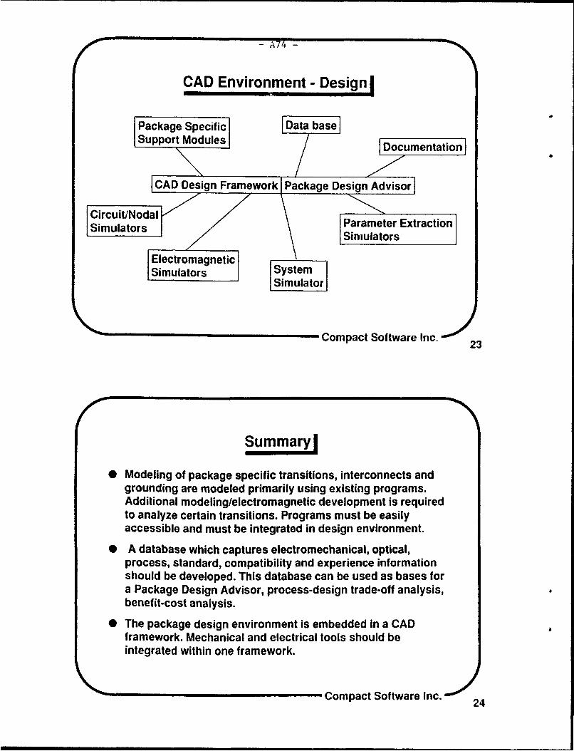
CAD Environment - Design !
Package Specific Data baseSupport Modules Documentation
CAD Design Framework Package Design Advisor
*imu iodelig o p arameter ExtractionSiimulators
Eelectromagnet ic
t imulators itioSystema Simulatori
p eaCompact Software Inc.f 23
Summaryl
a odeling of package specific transitions, interconnects andgrounding are modeled primarily using existing programs.Additional modelIing/electromagnetic development is required
to analyze certain transitions. Programs must be easilyaccessible and must be integrated in design environment.
"f A database which captures electromechanical, optical,process, standard, compatibility and experience information
should be developed. This database can be used as bases for
a Package Design Advisor, process-design trade-off analysis,
benefit-cost analysis.
"• The package design environment is embedded in a CAD
framework. Mechanical and electrical tools should be
integrated within one framework.
,,,, -- -Compact Software Inc. 224
Advanced Technology
APO - A75 -
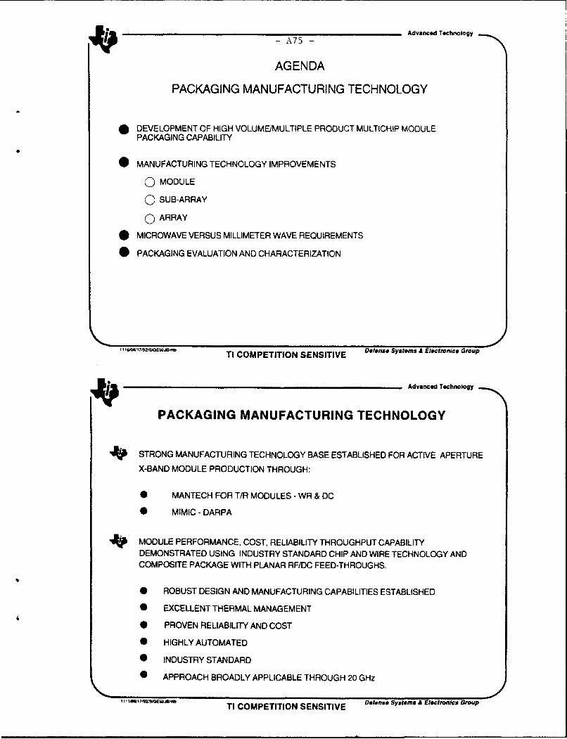
AGENDA
PACKAGING MANUFACTURING TECHNOLOGY
i DEVELOPMENT OF HIGH VOLUMEIMULTIPLE PRODUCT MULTICHIP MODULE
PACKAGING CAPABILITY
* MANUFACTURING TECHNOLOGY IMPROVEMENTS
o MODULE
o SUB-ARRAY
o ARRAY
* MICROWAVE VERSUS MILLIMETER WAVE REQUIREMENTS
• PACKAGING EVALUATION AND CHARACTERIZATION
I I tIMI 7,9MGMEA31f TI COMPETITION SENSITIVE Defense Systems A Electronics Group
Advanced Technology
PACKAGING MANUFACTURING TECHNOLOGY
4• STRONG MANUFACTURING TECHNOLOGY BASE ESTABLISHED FOR ACTIVE APERTURE
X-BAND MODULE PRODUCTION THROUGH:
* MANTECH FOR T/R MODULES - WR & DC
• MIMIC - DARPA
4 MODULE PERFORMANCE, COST, RELIABILITY THROUGHPUT CAPABILITYDEMONSTRATED USING INDUSTRY STANDARD CHIP AND WIRE TECHNOLOGY ANDCOMPOSITE PACKAGE WITH PLANAR RF/DC FEED-THROUGHS.
• ROBUST DESIGN AND MANUFACTURING CAPABILITIES ESTABLISHED
* EXCELLENT THERMAL MANAGEMENT
* PROVEN RELIABILITY AND COST
• HIGHLY AUTOMATED
* INDUSTRY STANDARD
* APPROACH BROADLY APPLICABLE THROUGH 20 GHz
.... . .. lwATI COMPETITION SENSITIVE ODfnse. Systems A Electronics Group

-A76 -
Advaimed Technoloy
PACKAGING MANUFACTURING TECHNOLOGY
4 PERFORMANCE DRIVEN REQUIREMENTS REQUIRING IMPROVED MULTICHIP MODULEPACKAGING CAPABILITY.
* BROADBAND ACTIVE APERTURE SYSTEMS
o INCREASED FREQUENCY AND DECRFASED MODULE TO MODULE SPACINGREQUIRES LOW COST, HIGH PERFORMANCE MULTILAYER RF/DC DISTRIBUTIONNETWORK CAPABILITY.
o INCREASED EMPHASIS ON LIGHT-WEIGHT PACKAGING
o IMPROVED MODULE TEST CONNECTION PROBES AND PROCEDURES
* CONFORMAL ARRAY ACTIVE APERTURE SYSTEMS
o THIN SKIN REQUIREMENTS REQUIRE 3-D RF/DC PACKAGING APPROACH
o AFFORDABILITY IS KEY ISSUE
0 LIGHTWEIGHT AND STRUCTURAL INTEGRITY REQUIRED AS WELL
TI COMPETITION SENSITIVE Defense Syftems A Electronics Group
Advanced Technology
MANUFACTURING TECHNOLOGY ISSUESAND PROPOSED SOLUTIONS
1.) IMPROVED ELECTRICAL MODELING AND SIMULATION CAPABILITIES.
- TO ACHIEVE INCREASED PACKAGING DENSITIES AND HIGHER PERFORMANCE FORMULTILAYER PACKAGING STRUCTURES, IMPROVED EM SIMULATION, DESIGN GUIDELINESAND DESIGN RULE CHECKING CAPABILITIES. EM SIMULATION TO ADDRESS IMPROVEDISOLATION AND VSWR FOR HIGH DENSITY THREE DIMENSIONAL PACKAGING STRUCTURESAND HIGH DENSITY MIXED MICROWAVE/DIGITAL PACKAGING STRUCTURES.
. IMPROVED MODELING TOOLS FOR COPLANAR WAVEGUIDE AND STRIPLINE STRUCTURES
2.) STATISTICAL AND ROBUST DESIGN METHODOLOGIES
- APPLICATION OF DESIGN AND STATISTICAL PROCESS CONTROL METHODOLOGIES TOACHIEVE HIGH PERFORMANCE, LOW COST AND FIRST PASS DESIGN SUCCESS THROUGHDEVELOPMENT AND APPLICATION OF STATISTICAL DESIGN AND ROBUST DESIGNTECHNIQUES, SUCH AS: DESIGN OF EXPERIMENTS AND RESPONSE SURFACE DESIGNAPPLIED TO ELECTRICAL, MECHANICAL AND FABRICATION, AND ASSEMBLY PROCESSES.
3.) SYSTEM LEVEL ANALYSIS AND APPROACH
- INTEGRATED SYSTEM ANALYSIS AND APPROACH FROM CHIP DESIGN TO ARRAY DESIGNIN CONJUNCTION WITH FOCUSED TECHNOLOGY EFFORTS.
Ti1 #% -• i ,ri ,iso r- Defense Systems A Electronics Group

- A77 - Advanced Technology
4 MANUFACTURING TECHNOLOGY ISSUESAND PROPOSED SOLUTIONS
(CONT.)4.) HIGH DENSITY PACKAGING CONCEPTS
- THREE DIMENSIONAL, FULLY ISOLATED, LOW LOSS RF/DC PACKAGING STRUCTURESCAPABLE OF HIGH INTERCONNECT DENSITIES AND HIGH POWER DISSIPATINGCAPABILITIES AND APPLICABLE TO CONFORMAL ARRAYS.
- HIGHER FREQUENCY AND LARGE ARRAYS REQUIRE INCREASED DENSITY ANDIMPROVED DISPERSION AND LOSS ACHIEVABLE THROUGH FIBER OPTICINTERCONNECTS
- ISSUES INCLUDE FIRST, SECOND AND THIRD LEVEL OPTICAL INTERCONNECTTECHNOLOGIES
- IMPROVED COOLING CAPABILITIES FOR BOTH SILICON AND GaAS COMPONENTS-MULTICHANNEL COOLING, THINNED DEVICES, INTEGRAL HEAT SINKS
5.) IMPROVED PROPERTIES, CHARACTERIZATION, CONTROL AND UNDERSTANDING OF THEINTERRELATIONSHIP BETWEEN AND AMONG RAW MATERIALS AND THE PACKAGESTRUCTURE
METAL CONDUCTORSIMPROVE MATERIALS-AG, CU FOR LOWER LOSSIMPROVED EDGE CONTROL-SHAPE AND POROSITY FOR LOWER LOSSESPECIALLY LOW TEMPERATURE COFIRED CERAMIC
CERAMICS
HIGH THERMAL CONDUCTIVITY,MATCHED GaAS AND SILICON SUBSTRATEMATERIALS
I I,1Z#A,17Mr1 J, TI COMPETITION SENSITIVE Defense Systems & Electronics Group
Advanced Technology
4 MANUFACTURING TECHNOLOGY ISSUESAND PROPOSED SOLUTIONS
(CONT.)INORGANIC COATING
LOW TEMPERATURE, POLYMER FILM COMPATIBLE MATERIALS TO PROVIDEMOISTURE PROTECTION AND ELIMINATE NEED FOR SEPARATE HERMETIC HOUSING!LID
POLYMER FILMSTAILORABLE COEFFICIENT OF THERMAL EXPANSION (CTE)
LOWER DIELECTRIC CONSTANTSTAILORABLE DIELECTRIC CONSTANTSPHOTO DEFINABLE POLYMIDE WITH SLOPED EDGES
ADHESIVES
TAILORABLE CTEADJUSTABLE CURE TEMPERATURESTAILORABLE DIELECTRIC CONSTANTS
SOLDER
TAILORABLE CTE
FLUXLESS, LEAD FREE MATERIALS
IMPROVED PACKAGES/SUBSTRATE MATERIALS
HIGHER THERMAL CONDUCTIVITYPRECISION MOLDING CAPABILITYTAILORABLE/MATCHED CTE
"TI COMPETITION SENSITIVE Defense Systems A Electronics Group

- A78 Advanced Technology
MANUFACTURING TECHNOLOGY ISSUESAND PROPOSED SOLUTIONS
(CONT.)
6.) HIGHER CHIP FUNCTIONAL DENSITY
SYNERGISTIC PACKAGING/CHIP DEVELOPMENT APPROACH
MIXED DIGITALJMICROWAVE-HBT TECHNOLOGYTTL/CMOS CONTROL CIRCUITS FOR GaAS MICROWAVEMONOLITHIC INTEGRATED CIRCUITSLOW NOISE AMPLIFIERS, POWER AMPLIFIERS,MIXERS AND SWITCHES
COUPLERS, BIAS NETWORKS, MULTILAYER STRUCTURES
7.) HIGH SPEED FULLY FUNCTIONAL TESTING OF DIGITAL, ANALOG AND MICROWAVECOMPONENTSINEXPENSIVE, HIGH FREQUENCY LARGE AREA HIGH SPEED PROBES
8.) HIGH SPEED INTELLIGENT PROCESSING
HIGH SPEED FULLY AUTOMATIC, FABRICATION AND ASSEMBLY EQUIPMENT ANDPROCESSES CAPABLE OF PRECISION PLACEMENT ACCURACIES WITH ADAPTIVECONTROL THROUGH INTELLIGENT PROCESSING CAPABILITIES
9.) DEVELOPMENT OF AN INTEGRATED DESIGN, ASSEMBLY AND TEST DATA BASEFOR ANALYSIS, SIMULATION AND PRODUCT/PROCESS IMPROVEMENT.
TI COMPETITION SENSITIVE Defense Systems £ Electronics Group
Advanced Technology
INTEGRATED DATA BASE
o ESTABLISH APPROPRIATE HARDWARE AND SOFTWARE LINKS BETWEEN EXISITNGCAECAD SYSTEMS TO REDUCE DESIGN TO BUILD CYCLE TIME
o ESTABLISH APPROPRIATE HARDWARE AND SOFTWARE LINKS BETWEENMANUFACTURING INFORMATION SYSTEMS AND EQUIPMENT SENSORS FOR SPCDATA COLLECTION.
O IMPLEMENT NEW DATA ANALYSIS SOFTWARE TO SUPPORT:
SPC, WHERE DATA IS INCORPORATED IN A REAL-TIME FEEDBACK LOOP FOREITHER MACHINE ADJUSTMENT OR TO FLAG OUT-OF-SPEC CONDITIONS.
DATA ANALYSIS, WHERE DATA ARE ANALYZED AFTER THE FACT TO DISCERNCORRELATIONS AMONG INPUT PARTS AND MATERIALS, OPERATING CONDITIONS,AND THE PERFORMANCE AND COST OF END-ITEM MODULES.
TI COMPETITION SENSITIVE Defense Syat*ma & Emectroncs Group

- A 79 - Advanced Technology
INTEGRATED DATA BASE(CONT.)
- SYSTEM SIMULATION, WHERE PERFORMANCE PREDICTIONS AT THE MODULELEVEL AND AT THE HIGHER SYSTEM LEVEL ARE MADE AND COMPARED TOMEASURED PERFORMANCE
- MACHINE SETUP OR OPERATOR INSTRUCTIONS, TO SIMPLIFY THE START-UPACTIVITIES FOR AUTOMATED ASSEMBLY OPERATIONS BY PROVIDING NEEDEDDATA ON PARTS AND MATERIALS
QUALIFICATIONS, FOR RELIABILITY ASSURANCE AND TO PROVIDE AN ARCHIVALRECORD FROM WHICH TO ANALYZE FIELD FAILURES
COST MODELING, TO ALLOW REAL-TIME COST DATA TO BE USED TO OPTIMIZEASSEMBLY LINE LOADING AND TO SUPPORT FORWARD PROJECTIONS OF COSTIN HIGH-VOLUME PRODUCTION
TI COMPETITION SENSITIVE Defense Systems & Electronics Group
____Advanced Technology
MANUFACTURING TECHNOLOGY ARRAYAND SUB-ARRAY NEEDS
4 ARRAY AND SUB-ARRAY FABRICATION, ASSEMBLY AND TEST ISSUES REQUIRINGMANUFACTURINC TECHNOLOGY iMPROVEMENT OF MATERIALS, PROCESSESAND EQUIPMENT.
* AUTOMATED ASSEMBLY OF T/R MODULES INTO ARRAY/SUB-ARRAY
U 'IODULE INTERCONNECTION AND ATTACHMENT
* AUTOMATED FABRICATION AND TEST OF DC AND RF MULTILAYER CIRCUITS
0 AUTOMATED FABRICATION AND ASSEMBLY OF ANTENNA ELEMENTS INTO
FACEPLATES
* AUTOMATED FABRICATION OF LIQUID COOLED COLDPLATES
0 AUTOMATED TRANSFER OF 3-D DESIGN MODELS TO FABRICATION SHOPS
* ELIMINATION OF CFC's AND LEAD BASED SOLDER
4I ? s1&'e.•r e eofons ystem & E ectronice Group
0- A80) Advanced Tochnotogy
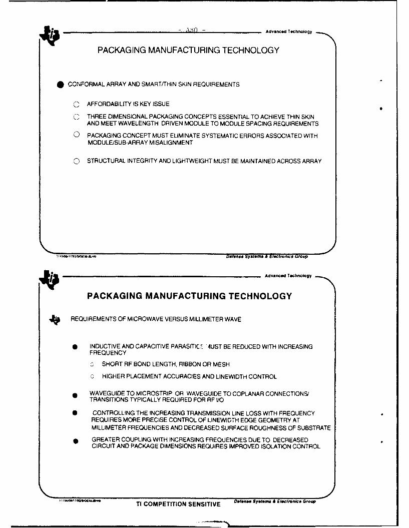
PACKAGING MANUFACTURING TECHNOLOGY
* CON;FORMAL ARRAY AND SMART/THIN SKIN REQUIREMENTS
OAFFORDABILITY IS KEY ISSUE
O THREE DIMENSIONAL PACKAGING CONCEPTS ESSENTIAL TO ACHIEVE THIN SKINAND MEET WAVELENGTH DRIVEN MODULE TO MODULE SPACING REQUIREMENTS
o PACKAGING CONCEPT MUST ELIMINATE SYSTEMATIC ERRORS ASSOCIATED WITHMODULE/SUB-ARRAY MISALIGNMENT
O STRUCTURAL INTEGRITY AND LIGHTWEIGHT MUST BE MAINTAINED ACROSS ARRAY
•,l T2,$ .,AV alens' systems A f lectrfnicCs Group
Advanced Technology
PACKAGING MANUFACTURING TECHNOLOGY
4 REQUIREMENTS OF MICROWAVE VERSUS MILLIMETER WAVE
* INDUCTIVE AND CAPACITIVE PARASITIC A 4UST BE REDUCED WITH INCREASING
FREQUENCY
o SHORT RF BOND LENGTH, RIBBON OR MESH
HIGHER PLACEMENT ACCURACIES AND LINEWIDTH CONTROL
* WAVEGUIDE TO MICROSTRIP OR WAVEGUIDE TO COPLANAR CONNECTIONS/TRANSITIONS TYPICALLY REQUIRED FOR RF VO
* CONTROLLING THE INCREASING TRANSMISSION LINE LOSS WITH FREQUENCYREQUIRES MORE PRECISE CONTROL OF LINEWIDTH EDGE GEOMETRY ATMILLIMETER FREQUENCIES AND DECREASED SURFACE ROUGHNESS OF SUBSTRATE
* GREATER COUPLING WITH INCREASING FREQUENCIES DUE TO DECREASEDCIRCUIT AND PACKAGE DIMENSIONS REQUIRES IMPROVED ISOLATION CONTROL
TI COMPETITION SENSITIVE oofens Syilemsa hA VcimnkI Grou

8- Advanced Technology
PACKAGING MANUFACTURING TECHNOLOGY
4 REQUIREMENTS OF MICROWAVE VERSUS MILLIMETER WAVE - (CONT.)
* CLOSER GRID SPACING WITH INCREASING FREQUENCY FOR PHASED ARRAYAPPLICATIONS PUTS INCREASING DEMANDS ON HIGH DENSITY PACKA(i!Nr-CONCEPTS.
o OVERHEAD FUNCTIONS SUCH AS PACKAGE SIDEWALLS BECOMEMAJOR ISSUE AT MILLIMETER WAVE FREQUENCIES
* BOTH MICROWAVE AND MILLIMETER WAVE APPLICATIONS REQUIRE MODULEMANUFACTURING TECHNOLOGY IMPROVEMENTS DESCRIBED PREVIOUSLY.
,,1,&,I, • TI COMPETITION SENSITIVE Defense Systems A Electronics Group
Advanced Technolgy
PACKAGING MANUFACTURING TECHNOLOGY
4IMPROVEMENTS NEEDED TO EVALUATE AND CHARACTERIZE PACKAGE MATERIALS,SUBSTRATES AND HOUSINGS FOR MULTICHIP MODULES
* STANDARDIZE)D TEST STRUCTURES AND TEST METHODS
o DEFINITION OF REQUIREMENTS VERSUS APPLICATION
0 IDENTIFICATION AND DEVELOPMENT OF TEST METHODS
0 DEVELOPMENT OF TEST STRUCTURES
* IMPROVED 3-D MODELING CAPABILITY FOR ELECTRICAL AND MECHANICALANALYSIS
* IMPROVED AND VALIDATED COST MODELING TOOLS
"TI COMPETITION SENSITIVE Delon", Sytems & Electroics Group

- A82 -
OAVANTEK
MULTICHIP PACKAGING FORMICROWAVE COMPONENT APPLICATIONS.
Mit-Standard and Commercial Approaches.
Oblectivesn
1. To describe differences and common aspectsof the two approaches.
2. To provide insight into the evolution of the microwavepackage in response to downward cost pressures.
3. To explore the OML concept for microwavepackages and components.
4. To provide ideas for leveraged packagedevelopment for low-cost microwave packaging.
John R. TylerJune 18, 1992.
MA FACItRI"
F OAVANTEK
MULTICHIP MICROWAVE PACKAGING: AN OUTLINE
MUil Standard vs. Commercial:
1. Requirements of the Microwave Package.
2. Avantek Case Studies.
3. Standards and Standardization.
4. QML Issues.
5. Leveraged Microwave Package R&D.
J, JVPAC'1VP .IJK•

- A83 --
F- OAVANTEK
REQUIREMENTS OF THE MICROWAVE PACKAGE.
* THE ELECTRICAL INTERFACE.
* THERMAL STABILITY.
- THE MECHANICAL INTERFACE.
* ENVIRONMENTAL PROTECTION.
* DFX -0TC.
HOW DO THESE CLASSICAL REQUIREMENTS DIFFERIN MIL-STANDARD AND COMMERCIAL PRODUCTS?
MANWUACT1URING
S•o AVA N TE K
ELECTRICAL PACKAGE REQUIREMENTS
Mil-Starsdard
* 0.1 - 0.2 dB insertion loss @ 10 GHz,VSWR = 1.2:1 typical.
0 Coax-to-microstrip transitions.
* Microstrip-stripline-microstrip in ceramic.
Commercial
* 1 dB insertion loss, 1.5:1 VSWR acceptable.
* CPW, Microstrip surface-mount configurations.
° Advantages: Lighter, cheaper, high-volume.

- A84 -
F G AVANTEK
THERMAL REQUIREMENTS
Mil-Standard"• Greater operating and storage temperature
range (ambient).-e.g., -55 to 95oC typ. operating range.
"* More GaAs--*more stringent package
thermal requirements.
Commercial
Higher package stresses due to materials.
Lower-cost package elements can bethermally insulative (eg, soft-boards).
• Advantages: Low fabrication costs.
S...... MUA,'O~C27TRZMI
F OAVANTEK
MECHANICAL PACKAGE REQUIREMENTS.
Mil-Standard
• Custom or semi-custom installation (outline).
* 100% mechanical screening.
Commercial
- MCMs: Some standard footprints emerging by market.
* FCPs: Surface Mount, standard SOT, SOIC packagesper EIA, EIAJ, JEDEC.
* Advantages: Open Tooling, Automated assembly,mechanical qualification by package.

- A85 -
F OAVANTEIK
ENVIRONMENTAL PROTECTION
Miu-Standard
"* Seal per 883, Method 1014.
"• Finish: Noble metal or solderability per M-38510.
Commercial
"* Product qualification to high capability (Cpk>1.33).
"* Process qualification to high capability (Cpk>1.33).
"• Open-package (cavity) qualification at supplier.
* Advantages: Higher product quality at lower cost.
MANuFA Cr•.RTJG
F- GAVANTEK
DESIGN-TO-COST
Mil-Standard
"* Parts count reduction (MANTECH).
"* GaAb cost reduction (MIMIC).
* Custom designs - low non-recurring investment.
Commercial
"* Typical $50K - 100K non-recurring tooling--0 low unit price (in volume).Eg, stampings, castings, moldings.
"• Standardization of package outlines.
• Advantages: Open tooling, volume manufacturing.
S' • .'•2• w A c'•uR".•

OAVANTEK - A86 -
MILITA RY --- COM M ER CIA L
COMPONENTTYPE: TO PLANAR-PAK SMT W/CARRIER SMT GULL-WING LEADLESS
AMP 0 1b
AGC___1
VTO
DET 0
mix 0
ATT 0
LIM-
SWT 0 1
O AVANTEK
cz0
U --I: E- ME- /
&--
<J E- V
MAWACTB I

0 AVANTEK - A87 -
i. *• L .• in
IIj I
--iii!f ,II L---4i-• I,S, . l7,l.-I T
j ;dl Inhit I(• -"5"
(D'.
I Iii I iiMANUFACTURING
F OAVANTEK
POLYMERIC ENCAPSULANTS
MATERIAL DIELECTRIC DISSIPATION HARDNESS LINEARDESCRIPTION CONSTANT FACTOR@IMHZ TCE (ppm/oC)
ABLEBOND 2.2 0.019 60D 30933-1,5
DOW CORNING 2.8 0.001 44A 20001-4939
CHIPCOAT 2157 2.2 0.0036 9H 7
SUMITOMO BAKELIT 4.7 0.015 65D 20NOVOLAK COMPOUNt
AIIUIACTURINI

- A88
ENCAPSULANr FECT Q 2-6 Z
FAir Encapsulated
input R. L. 13.1 10.8
Gain 12.6 11.5
Noise Figure 0.98 1.13
Ceramic & Glass - Metal Packages
Commercial/industrial GradePKG Codes 18, 35, 36, 72, 76
Surface MountGold plated Kovar leadsGlass-Metal
Surface MounitTin plated Kovar Leads 72
18 ~~A1203ceai
18 ceramic "0-72" Meta a
+ 76 Gold plated Kovar leads
TXV, B and C Level Screening

- A89 -
&OAVANTZI(
COMPARISON OF THE TWO TECHNOLOGIES
PACKAGE#18AAE#2OXIDE METAL BONDING COFIRED ALUMINA BONDING
MECHANICAL INTEGRITY DEPENDS ON: MECHANICAL INTEGRITY DEPENDS ON:
*WETTING CONTACT ANGLE *MONOUTHIC STRUCTURE OF CERAMIC LAYERS*TCE MATCHING*STRESS PROPAGATION PROPERTIES OF GLASSSTRUCTURE*CORROSION PROPERTIES OF KOVAR
CERAMIC PACKAGE SECTION VIEW
GLASS PACKAGE SECTION VIEW
-1SQUARE `I0 MAX SQUARE
.400 MAX
.400 MAX
,. 4o1Mo1S* ,~*.*)..., ,,ADVANCED BIPOLAR PRODUCTS .-- r
F GAVANTEK
COMMERCIAL PACKAGE STANDARDS
0 JEDEC STANDARD No. 26 General Specification..."
No. 26-A
No. 22-B "Test Methods
JEP No. 95-1 "Registered and Standard Outlines..."
JC11.5-91 Standards Committee.
0 EIAJ '- . EIA
* ISO 9000 Europe, Japan, Korea, Taiwan.
-_MA14UPACTVRXIV

- A90 -
Plastic Packages
CommerciallConsumerPKG Codes 04,05,08,11,84,85,86
"SOT-143"
+8 0 8
L_4 Surface Mount "S0-8"
+ 4 Tin plated copper leads Surface MountTin plated Kovar leads
Tin plated copper leads
OAVANTEK
Rellability Qualification For Plastic PackageTest
Stress Test Methods Test Condition LTPD Duratlon
SJEDEC STD Tj/Tch temperature
Operating Life Test 22B @b 2000 hours
M-At08
i High Temperature JE0ECSTO Ambient temperature
Reverse Bias' 228 Am01n 5 1000 hoursM-At08 @15C
High Temperature JED ST Ambient temperatureStorage 228 1000 hours
M-At03 @ 1S0C no bias
JEDF-C STD Temperature from
Thermal Shock 228 -65*C to 150*C 7 100 cyclesM-AI06
JEDEC STD Temperature from
Temperature Cyciing 22B -658C to 150°C 10 1000 cyclesM-A104
Temperature & JEOECSTD 85,C/85% Relative1 Temeratre &228
S Humidity 28 Humidity 10 1000 hoursHumidityM-A10t
SJEDEC STO 2 ATM saturated steam
Autoclave 228 +12i*C and 100% 1 0 96 hours
M-A102 Relative Humidity
'Applicable only to Silicon Bipolar Products. Appendix B
L MAWFACvUR'IMM

- A91 -
OAVANTEK
QML SUPPLIER REQUIREMENTS
"w Standard differentiation of processesby component or package type.
- Assured capability (Cpk) of each process.
Product qualification, package qualification.
Circuit topology and layout can be custom.
Significant component cost-reductionto system-level contractors.
MANUFACTURNMG
O'AVANTEK
QML PROCESS CAPABILITY
QUESTION: WHAT IS THE CUSTOMER'S REQUIREMENT?WHAT IS THE PRODUCT REQUIREMENT?
QML SPECIFICATION: DETERMINE MINIMUM PROCESS CAPABILITIESREQUIRED BY PACKAGE OR PRODUCT.
QUALIFY PRODUCT AND SHIP VOLUME.
KMANUACUINGXM

- A92 -
-" OAVANTEK
OML PROCESS CAPABILITY883, METHOD 2011: DESTRUCTIVE BOND PULL IS THE BEST METHOD
TO DETERMINE PROCESS CAPABILITY OF WIRE-BONDING. SPECIFICATION LIMITS ARE NOT SCALEDTO AVERAGE BOND STRENGTHS BY WIRE DIAMETEROR BONDING PROCESS.
METHOD 2019: THERE IS NO CORRELATION BETWEEN DIE SHEARSTRENGTH AND ELECTRICAL RESISTIVITYFOR AuSI EUTECTIC OR EPOXY DIE ATTACH.DIE SHEAR TESTING IS NOT SUFFICIENT FORHIGH DIE ATTACH PROCESS CAPABILITY.
METHOD 2017: FILLET REQUIREMENTS ARE NOT SUFFICIENTFOR GaAs POWER.
NEW STATISTICAL ELECTRICAL RESISTIVITY."KEY MEASURES:"
THERMAL RESISTANCE BY IR SCAN.
TRANSIENT THERMAL AND ELECTRICAL RESPONSES.
"0" CIRCUIT FOR WIREBOND AND DIE ATTACH QUALITY.
RADIOGRAPH, SAM NON DESTRUCTIVE TESTS.
MAMUFACTrJRZM
OAVANTEK
PACKAGE DEVELOPMENT PRIORITIES
* STANDARD, LOW-COST, SURFACE-MOUNT COMPONENTS-PACKAGE QUALIFICATION.
* STANDARDIZED PACKAGE OUTLINES--0- TOOLINGINVESTMENT -- o-PACKAGE COST REDUCTION.
-INCLUDE TEST FIXTURING AS PART OF STANDARDPACKAGE DEVELOPMENT.
PARTS COUNT REDUCTION -*'INTEGRATE ADVANCEDMATERIALS WITH LOW COST MATERIALS.
Examples: Aluminum MMC ---- A356 Al, Cast.Ceramic-Metal Composites -PAI, Cu.Polymer-Polymer Composites --oEpoxy Resins, Molded.
USE EXPENSIVE MATERIALS ONLY ALONG THE CRITICAL PATH.-ELECTRICAL, THERMAL, MECHANICAL.
FAVOR LESS DEGREES OF FREEDOM IN FABRICATION.
MANUMFACTUR1W$

- A93 -
F GAVANTEK
PACKAGE DEVELOPMENT PRIORITIES
' GaAs FLIP CHIP BONDING - CPW TRANSMISSION LINES.
* POLYMERIC ENCAPSULANTS.
LOW-COST CERAMIC INTERCONNECT STRUCTURES.
ORGANIC MATERIALS FOR PACKAGING, INTERCONNECT
AND BONDING.
SJAU FA C'•MJR.
GAVANTEK
LEVERAGED MICROWAVE PACKAGE R&D
* SHAREHOLDERS (INDUSTRY) TO DRIVE EXISTING CONSORTIA
IN MICROWAVE PACKAGE R&D.-UNIQUE REQUIREMENTS -UNIQUE PROGRAM.
* GOVERNMENT/INDUSTRY TEAMS TO DEFINE R&D OBJECTIVES.
o STANDARDIZED QPL COST ROADMAP: 5 - 10 FORM FACTORS BY '93.
* FUNDING THROUGH CONSORTIA TO KEEP PACKAGING OPEN,
STANDARD AND NON PROPRIETARY.
MANWUAC7TUJUN

- A94 -
AIM Packaging: Commercial vs. Military
OTIIINE
0 Packaging Objectives
a Baseline Packaging- Military- Commercial. Conclusions
a Recent Trends in Packaging
* Possibilities for the Future
9 Recommendations
Rick PerkoJune 18, 1992
Packaging Objectives
MILITARY- Reliability (MTBF & Shelf Life)- Moderate Cost (Low - Medium Volume)- High Perfomance (Thermal & RF Characteristics)- Size (Highly Integrated)
COMMERCIAL- Low Cost (High Volume)- Quality (Uniform Performance)
Standardized Interface

-A95-
S XBaseline Technologies / Military
Hermetic Metal Enclosures
Coax Glass-fired Feedthroughs
Welded Covers
Ceramic Packages
- Co-fired "Planar" Feedthrounhs
- Covers Welded, Soldered or Glass Sealed
Metal Package
Cost $50.00 - $200.00
i -Material Choices for: | -Matrix Metals I
Extremely Adaptable Advances
Weight Powdered MetallurgyThermal Conductivity
TCE- Complex Partitioning for Isolation- Excellent RF Performance

- A96 -
A Baseline Technologies / Commercial
* Plastic Injection Molded- 3 GHz Frequency Limit- Non-Hermetic
a Plastic Premolded- Non-Hermetic- Performance Limits Undefined- Applies to Chip on Board
e Mini-Ceramic- Hermetic
- Higher Performance / Cost
a Discrete on PCB- Depends on Cheap Labor- Integration Potential Limited
Injection Molded Package
Dice Wafer
Unit Cost (Korea) Die Attach < $0.25Wire BondInjection Mold
1 j
Four Bit Attenuator
3GHz LimitTechnical Advances: Low Inductance Lead-frame Design.
Multiple Die / Package.

- A97 -
A Premolded Package
Circuit Size .8"X.8" Cost < $1.00
A A
-06A-A .
Useful for Chip-on-Board Assemblies.Non-hermetic.No Microwave Optimized Standard Packages.
AI'C•t Mini-Ceramic Package
Cost: $1.25Package Size: .250" X .215" X .050"Circuit Size: .120" X .120"
GPS Low Noise Amplifier
Hermetic I Surface MountLimited to Smaller Circuits

- A98 -
Sl Baseline Technologies / Conclusions
Plastic Commercial Packaging Does Not MeetHermeticity or Performance Requirements of
Many Military Applications.
Ceramic Packages Can be Cost Effective for
Small Circuits but is Expensive for Larger HighPerformance Assemblies.
% Current Trends
Reliability Without Hermeticity
. Better Focus on Actual Failure Mechanisms
- Surface Passivation Options
Lower Cost Hermetic Enclosures
- Integrated Package / Circuit FunctionsLTCCWafer Level Protection
- Powdered Metallurgy
Acceptance of Plastic?

- A99 -
SMPlastic
Unreliable or Unappreciated?
Injection Molding Technology is Evolving Rapidly
- Compounds, Fillers & Methods Have ImprovedDramatically in the Past 5 Years.
- Reduced Moisture Intrusion
- Improved RF & Thermal Performance
Premolded Technology Also Holds Promise
- High Strength Crystalline Material
- Integrated Heatsinks
- Metal Coatings
- Complex Forms
THE COMPLEX WORLD OF PLASTICS REQUIRESCONTINUOUS EVALUATION TO DETERMINE
THE IMPACT OF RECENT ADVANCES
46c" Microwave MCMs
Intermediate Motherboards le.g. GMICIversus
Integrated Packaging (e.g. LTCC)
MCM Integrated Package
Strengths StrengthsPartition for Yield Control Reduced Parts CountPartition for Performance Includes PackageIncreased Flexibility Liabilities
Liabilities Premium on Known Good DieRequires Final Package Integ. Medium Dictated byIncreased Parts Count Package Needs

- AIO0 -
S cPossibilities
Hermetic MCMs
* Glass / Silicon (GMIC) Integration Medium- Wafer Level Protection
- High Performance Potential
. Cnmpatible with Flip Chip & Thermal Pedestals
Plastic Enclosures
* Premolded Plastic Enclosures. Integrated Heatsinks
. High Strength Crystalline Plastics
. Complex Structures (Multiple Chambers)
. Metallized for EMI
* Recommendations
RWoH Programs- Microwave Applicability- Failure Mode Analysis- How to Qualify New Technologies
* Plastic Technologies Programs- Reliability Issues- High Frequency Transition Methods- Thermal Management- EMI Control
e Don't Bet on a Single Solution- A Broad Spectrum of Requirements Will Require
Flexible Solutions.
@ Technology Access- Second Tier Suppliers are Critical for Broad Leverage.

- A•Ol -
Microwave Packaging Technology Workshop18-19 June 1992
Military vs. Commercial PackagesMultilayer Ceramic Package Technology
Michael FlandersCoors Electronic Package Company
""Commercial vs. Military"
" Packaging has traditionally been down the supplier foodchain; not as affected by "peripheral" requirements
"* Increasing complexity/capability of packaging, plusrecent Govt. focus brings opportunities/responsibilities
* Focusing only on technical requirements will no longersuffice; must address non-technical aspects when quoting
* Many package manufacturers will need some "education"as Primes or co-Primes
Coors Electronic Package Company

- A102 -
SIGNAL DELAY
60%
N CHIP
M1 PACKAGE
25%400%/5/II !11111
75%
1970 1990
!MLC Technologies: MATERIAL
Material Applicatione Advantages Disadvantages
Aluminum Nitride - High Performance Packages 0.1% Shrinkage Control - No metallized cavities
(AIN) - High Power Applications (hot-preased) (hot-pressed)
- Large Chip Packaging
Low Temp. Cotlred - High Performance Packages - High-conductivity metals Poor heat dissipation
Ceramic (LTCC) - Microwave Applications - Low K formulations
- Adjustable TCE
Alumina 99.5% - Thin Film Interconnects - Excellent Surface Finish - No collre metallizatlon
- Microwave Applications - Low Lose
Alumina 92% - Low & Intermediate - Low Cost
Performance Packages - High Strength
- Mature Technology
(Coors Electronic Package Company)

!M LC ech o .............
MLC Technologies: PROCESS
Process Advantages / Applications Disadvantages
Greenline transparency - Established technologies
to ceramic materials - Cost Control
Hot-pressing - Dimensional Control - no metallized cavities
(currently)
i Continuous furnace firing - High Volume Material-dependent
- Low Cost Shrinkage Control
Coors Electronic Package Company)
IMLC Technologies: PROCESS(cont.)
Process Advantages / Applications Disadvantages
Retire techniques - Curved Ceramic
("smart skin')
"Programmable grid' - Low Cost - Standard Grid
Via Technology - Short Turn limitations
- Hole Quality
Electroles$ Plating - Design - Not approved for some
military applications
CuW Thermal Vias - Lower Cost vs.
CuW heateink
(Coors Electronic Package Company)

-A104-
La La
tw CU
0 cd c
>04

MLC Technologies: PART TYPES
Part Type Applications
Feedthroughs -High-Rel replacement
for glass-to-metal seal
-Controlled impedance
Double-sided boards! Reduced signal delay
thru-board Interconnects -Component consolidation
Coors Electronic Package Company
Thini Filin
Wir -.,Integrat d Structure
(b Iiiterofiiee
siedal c ofired cr ic carer. 1, Dulesieetallzaip oduen igim oie eai sum
iiilercnF7 777n7

A A106-
MLC Technologies: PART TYPES!
Multicthlp Modules Parortec ion ofil MCuom topdacakaofge wt pttr
Mutit, odleBaeforThitavntaeo F himil
Mumoihip Module /-Can combing substrateInterconnect Board and package
C004s Electronic Peckage Company
See. tin I,$w 40
Sele4viSJ.Arate~ for

- A107 -
MLC Technologies: PART TYPES(cont.)
Part Type 1 Applications
Brazed packages - PGAs, leaded packages,
housings, heatsinks
SLAM arrays - Array processing
(by customer)
Chip carriers - Standard outlines
Crystal / oscillator - Clock applications
packages
ýCoors Electronic Package Cornmpany
I Areads for Investment"* Combining different ceramics in single structure
(e.g. LTCC on AIN, high/low-K combined)
"* Lower loss LTCCs
"* Improved edge definition
* High-conductivity pattern metallization
* Higher conductivity internal metallizationfor high-alumina substrates
* Establishing via grid and lead pitch standards
* Economical methods for finer pitch vias(cost-controlled tooling)
* High-frequency testing techniques
(Coors Electronic Package Company)

A A108
E
SThermal Conductivity(W/m deg C)
Copper_--___ - - 398.0
Aluminum Nitride ~ 205.0
Copper/Tungsten __147.Q
Molybdenum 138.0
Silicon ____ 8.
Alumina 20.3
Kovar 18.4
LTCC 2.3 .
0.0 100.0 200.0 300.0 400.0 500.0

- A109 -
SThermal Expansion(ppm/deg C)
Alumina
Copper Tungsten 6.5Kovfar • e.0Ga~s •6.0
Molybdenumi, 5.4:Aluminum Nitride - - .... -.----.-- -- -4.7
Tungsten 45Mullite -. _ .. - •45
Silicon Carbide -•T•--- 3.8Silicon 3.5
LTCC 3,0Diamond •- 2.5
0.0 2.0 4.0 6.0 8.0
Coora Electronic Package Company
UUej•owl
V A
r.0
3 P 0 2Ll*~ 13 1
U
E~ rz0c

11 All -C
A -0
u ~a s ft (5
4Q 41
.5 0 -0
51 U1 -W-
410 12A)) z;
V' w
LI c,04

- AM!I -
Planned Activities for 1993
1993 M 'T-S Workshop on Low Cost Packaging
Special Issue of the- MTT Transactions on Packaging. 1993/1994
1993 MTT-S Packaging Session at the MTT.S Symposium
Recommendations
Central Source of Information Needed:
Broad Industry Access without Proprietary Considerations is Necessary
Materials PropertiesModelsSources of Packages. Parts, Matenals.StandardsDesign Rules
,tandards and Standardiration:
Standards are a Necessary Precondition to Standardization which is aPrerequisite to Cost Reduction
Standards are Needed in:TestModeling and DesignManufacturingEnvironmental RequirementsRuggedness
Standards Activities Need to Proceed More QuicklyNeed Consistent Effort for Vendors and Users to Develop andAdopt Standards
Packaging flesiga Rules'
Vendors Function Primarily as "Machine Shops' and have No MicrowaveDesign or Test Capability
Design Rule Compilations are Needed to Remove Barriers to Entry forParticular Packages and Ultimately Reduce Costs
Training in Microwave Package Design is a Necessity

- A1 12 -
E<00> E
AUTOMATIC RF TECHNIQUES GROUP
Call For PapersThe Autotnatc RF Techniques Group will hold their 4fth Confeence in Odindo. Florida, Dc-emuber 3 and 4, 1992. The Coference there is:
Measurement and Design of Packages andInterconnects
As nicrowave and digtal designs increase in complexity and speed. while they decrease Ln Size,the difficulty of re•lizing packages and interconnects is becorming a choke-point in design midMCa,3wemMnM The increased difficulty leads to lick of accurate data, which, is turn, can led tocatastrophic design costs aind lead-tnie. Papers am invited which kentify problens and/or solu-dons in this mae Potential topics include (and Am not lnited to) neasurencnt of large, highspeed. hiSh frequency systes; analysis of such systems; trouble-shootiOg or validating fabricatedsyso.ms (both dting manufacture and duing dcsgn); and application of microwave techniquesto high speed digicd systems. In addition, papers concerning all other armas of nicrowave mci-surement and design Am welcome.
Technical presentations shall be infonmn twnty-five minute talks using vivwgaphs or 35.-mslide illustrauons. Authort are requested to submit a on-pge abstract and a 500 to 1000 wordUWnsU Y with aaachn=nt containing illu.rstrons. etc., providing suficienc technical cowent :o
enable proper , ealuation and explaining the conuibudonss u.•eafness to the conference attend-ces. Pl refer to "ARFTG Instructions to Author'" for further infomation. All accepted paperswill be published in the post-conference digest. Two copies of the abstract and sumnmay shouldbe $ent to Bert BeM , Technic1l Program Chaian and should be received no later than Octo-bh 5,1992. Papes received on or before Septembr 7. 1992, will be considered for early accep.unce and pre-conference pubicity. Manufacturers intgresd in exlhibitng at the conferenceshould contact the Exhibit Chairma• for infora'ton and an apptication and agreement form.
Subrnt papers to: For Exhibhi Applications or fur-
Mr. Ben Berson shae informaoion contact the con-Berson and Associates ference chai•man:
655 G0 Wr Jam-es C. Rautmo"f4V• Cce "'V Mountain View, CA 94041 Sonnet Softwve, Inc.157-r ' 5 -ft 2 e415)969-2101 135 Old Cove Road, Suite 203
Liverpool. NY 13M-3746(315)433-3096

Al A13-
The materials data in this section was taken from data sheets and other literature from 'enclors.including published articles. Ariucle references ame identified by a code in brackets. for example
INOV9f]. the corresponding references are also compiled near' the end of this Handbijok-
Most numerical values are from tables, but some were obtained from graphs. Where nccessarv.A numerical values have been conversed to the standard units used in this Handbook. usuallv SI
("metric"); vendors' Originsal values are shown in braces I .For explanations and converstinfactors for units refer to Units & Conversions.. at the end of this Handbook ipage 1), Data givenfor room temperature. .5oC or 30'C are combined on the sanme row in the tables.
The data included here are usually the most recent and best available, and in many cases tasindicated) have been reviewed by the ',endor'. However. caution is warranted in using this data,Usually, values represent typical characteristics rather than specisication luimit. Vataoility int thievalues is seldom indicated, and frequently data values do not agree even among a single vendor'literature. in most cases, the values must be regarded as typical values, because of lot-to-lotvariations. If a property is critical, evaluation of fte particular nmateria~l lot, or agreement onspecification limits with the manufactumrer may be warranted.
Non-magneric means not fErromnagnetic.
Data for the following materials are included in this section:
(Generic Names Brand Namnes
Alloys
-Fe-Ni 42% to 50% Ni -
F*-Ni-Co ASTM F-15 Xova4., Sealva4*
MOWa MaltriX MleroueIMPOaltO
AglIinvae Silva(`
AlISi CMSH A-40
Al/SiC OWAL 20': S"C4 MCJJ. SiCSO MCM. SiCS5 MCM;PAIMEX': MCX-622", MCX4693". NX-2O1', NX-5221'" NX-5251`, EPX-s00'. EPX-20oo'
CuVAU20 3 GbdCopil AL- 15
Mo/Cu AMC 7525, AMC 8020. AMC 8515;Thwmkn& 70M, 65M:
iCMSH: CM-SO, CM-iS. CM-20
CMH Alu1n. W-15 W-2
Aluminum nitid. N

61 e
~I0 t7~ 0
In 0I ~ i
~ -' 0
-1 0 - F
w- -
IL. cc-
0. l~-Z.9 f
01~~~~t E1~. .Q~0.0
CD~0 . 0~ l 0 I C.0 0 Fin-(00 - 0~
>v z.o -~ '
a! EL ZI -o
:5 30 p
CL E .0 0<0r
; C4
0Z GVl

-A115-
.jE
R
2-6t
b; -j
w ri
JIL: -,L
Eo - L Zn S.
, LP', L -
Sol ~ --
2 w C.L"ti~flI2I.X L

E- A16
EL..
02
c~ no
L 9
'2 4
~ 0 0
(2tL 1'0 ' 01
E, Cc 0 1,4.
Cl3. 000
E z
c C E
>1 E

A117 -
CIL
0Ea
r=, U!
,.;
LL0 v
0F
CL I a cc
mIU I W
"
I (ol ., 0
, -') , C.) 0
C._ . . .( 0 0 . .,.0-F.- • +0 + u,+,
E 0
F I, I'i ' ; ) ' • -* S .- I F I F . 0
.0 j I tI Ft t I _ 0F F F F- 0. o
F"' + r ' m " + • ' l - - i -IN , F ' :• I 2 .. 2 •F '.) " I ,flI<, ,U. ,'+ ' F,,, +, ',.. . -F0 ' o •0 • +I
I i l , I + .I F ) l 0 • , I F F -
F * 0C+ - _
F F m+. o F F+F F ~F~ zoF F ~ ~, S ~ 0 .

A 1t8
Zb44
CL U3 --- 3 ~ 0
LL. -0-
a 06 CL4 4-
8 .04 1 q
U1
C~1 -.

- A119 -
�1 .4
S - ,I - (�4 -
0 3 0 - -
2 � .4, 0 0
SO 0 0 � 4,o ,e � a - -o �= :(-.j :4� .- 2 - 4�0 ('4 - �u, "'.4. -- ' 4.
E3, 4 0 0
9. 2
3 �. .0
I �4O I S - 4-: 4.
-� 0
.4 '4I -
C.) a0 8- '4
.4 -e@-��' '4 '4 '4
-c �0 (- � 0 -0 0 Ci3,. -�
�9I�0 0 (§r�0:�g. �E � - -______________________ U -. -- U,
-3
.�. �-
O 0
- (1
S -�
.4 .4
* .0.4 - 3- .c .4
0- �. .0
3 .0o '40. '1
5 5) -0 1
0 I- 0 .�
- .� (0 3S...
- 0 -�a. 3� S
�
44 A- E �I
-4 .4 0 **I 'jZ �0 � 0
� E � .fl.j4� aC-, I
.2to � E � 0
I�IE -...0 A 21114h S
-3 '3 -,0 0 E <� 04.0-COb.4 5-

- A120 -
_- i
.., -_-
"7-E
C. - .•
7, '4 _

- A 121 -
II
0: U 1
LP e
S .601
CO

-A122 -
-~ E0
00 2
w IL- z.
40
OS -S iCL -- o
* 0

-A123-
0 0
12 ~
c~ U-C
00
Z '6
S0'rn )o -j W~
T (a 0)Z L N
cx~
ci7i
II -a . 4 -N i -
0a ca r

A1M24-
InIL
A LL
.0
xi
U- .
>iiii

-A125-
I ZZ 2
U 0 M
IL 0. 2
Q a
- fi 7 0
.C .Eu ~ -a52 ~~C Z C<IF *~
LI) 2 LL ~

-A126-
ol
aa,
1.0 0r'
a, 0 W ~.IV CIL~-snf~e~ao,~~r
C- > 155-- . * .0 . 4.--~ ....
U.
s r
E a 00
z. c 0
2a C'
Cal
Lza: !e -

-A127-
( -E S
E . z
t4 4>04.
SE
~~ a
co ~ 0
E ta
cu~ L'-- Z .

-A128-
i U
cs:- -
~:~ K ---------- -
0 - 0
L C0 > 0(
w~ M
0~~~- 0 0o10-
- L -
0C 0
- 'o
0.0 l Q) Z
0
C c 0 C 0
0.

- A129 -
C.v
~'E QC
-. z.- " "
'-- A A -•
"
-I -•Z-
"" C
' L.n t; z
CL. z cm
-a
9 C'< IE ,i -
e~ E --
..... U ... A---
In A
o ~ ~ C -C A -C .
ccc
-- 1~~~~~
1
. . . ..
40..
.•
UU LL1
z -U
" C ,, • C

-A130-
I> C 0 0.
o8 0
; ,-1 *~ K-0. 0 00
0 cc
73,C
*
...n.
- N g5.E E
2A 5. W't s
C- P
C.
ii _
oo -0 IS
CLE E E>

-A131-
2z, z i 2
.0
J:
4: '4 .
4:e co -4. ..
M I co
K 2 auatV

-A132-
1- 0
_ _ i hr
07 c u
hr * 2 ., V
y N
""I 'i F I vl xhr D 7'
o ~ Q 14 f '2~~~;
sr~ 7
.7~~~ MO 8 ~- - N "
*~ =~' C0.0 .7 ~ hr~~?L)hr .. 7 N W N .hr~('4
lid
0 -N 0
hr~~~L Zi r 0
0 >co "I -Ir

-A133
E 5
E
2~ 7
E E: cco~ ~ I
EaU
E; F
411

-A134 -
S• - - i ° • • , • *
o0S. .. . ... . ... + "P a 1+S a +-''0 B.+ •
C,- +., -,.€.
+'+_ •P 0 C+ B + 0++ + 0-++0 c._ - O ,N t , 4' 0,4 4, t *. + flN N• N N , ++ 0 i
•, I 0 *0,. .,+
+ . .,2 S•. I 60
4+ , ,- I •
o4, e ° ++ + +4, + d i + ° +•' ; + +m
a++ i +- U 0' •

-A135-
722
CL-
0! EC
- '~.A
z;'.Z2 'S -
1' , L-LL4 cLL " .)
41 Q0 a 0 - 0.- '-.4.40.

-A136
72 -.
v'v
E~ Lf
v L;
du-- 1- - , -

- A137 -
C c
0 '
£ 3
, 0 w
in
" CL
0j -K
0 LA.

- A138 -
m 0031 I I
8
i I .... ~
I I • ° 55,
1.5-� r, E
p E
.0ca
IS, II • •
"I • SN ° :--
">c. - ._ •K--
-o m' ,.
,, 5-. .,
- U v
'S o Cc
u0 u
v alpc

- A139 -
I, o . :•, = -z z
C L ' o -U-- v04a E - 72
'-•. R' - ". - .
"a 0
In@
I I * m, E
0-I -; , ,t c ._
01
W d I - I 6 _i_
-- 2-
,• I -I

- A141 -
Commercial Software for Support of Packagxinp CAD/CAM
DATABASE:
Object Oriented: Relational:
VBASE INGRESGEMSTONE SQL SERVEROBJECTIVITY/DB INTERBASEOBJECT STORE ORACLE
PROGRESSINFORMIXUNIFY
GEOMETRY (Solids Modeling):
AUTOCAD * 0OM SOLIDS *CONCEPT MODELER* IDEAS EUCLID* CADDS 5 CAD KEY SOLIDS
Products marked by "*" have true 3-D capability
ELECTROMAGNETIC SIMULATORS:
"* ANSYS * HFSS EXPLORER"* MSC/EMAS * MAXWELL EMSIM"* MAFIA * SUPERFISH
Products marked by "" are true 3-D simulators
CIRCUIT SIMULATORS:
SUPERCOMPACT (Linear)HARMONICA (Non-linear)TOUCHSTONE (Linear)LIBRA (Non-linear)HEWLETT PACKARD
THERMAL SIMULATORS:
NASTRAN AIRCOOL NISATHERM 2 THEAT COMOS/MALGOR ANSYS

- A142 -
MECHANICAL SIMULATORS (Vibration, Stress):
PERSONAL DESIGNER NASTRANANSYS COMOS/MALGORNISA )
DRAFTING:
CADDS PERSONAL DESIGNERAUTOCAD CADKEY
)