active pixels for x-ray applications, implemented in a ... pixels were implemented on the side of an...
TRANSCRIPT

UNIVERSITY OF OSLO Department of informatics
Active pixels for x-ray
applications,
implemented in a
standard CMOS
technology
Master Thesis
Kristin Hammarstrøm
Løkken
August 2008


i
Preface
This master thesis concludes my work for the master’s degree in Microelectronic Systems at the University of Oslo (UiO), Department of Informatics. The research was carried out at SINTEF in Oslo. I would like to thank my supervisor Joar Martin Østby (Senior Scientist, SINTEF; Associate Professor, UiO) for guiding me through the process. My thanks to Morten Berg (WarmSystems, former research scientist at SINTEF) for setting up the test environment for my photo sensor circuit and to my fellow student Kjetil B. Stiansen for providing me with the operational amplifier from his master thesis and also for designing the PCB needed to test both our circuits. I would also like to thank Roy Bahr (Research Scientist, SINTEF) for his help in the time of need when the tapeout date was near and the pads refused to work properly. Special thanks to my parents for always believing in me, and my husband Bjørn Willy for his support and never ending patience.
Oslo, 31 July 2008
Kristin Hammarstrøm Løkken

ii

iii
Abstract
During the past ten years digital technology has entered the world of mammography. It has not taken completely over, however, because there are still disagreements as to whether the digital technology is as good as the analog at detecting breast cancer. The amount of radiation exposed to the patient is another issue, because larger amounts of radiations are used with the digital technology. To contribute to the improvement of the digital mammography technology, research has been done on the pixels used in the x-ray sensors. Different pixel architectures have been implemented in a standard CMOS technology and compared with respect to sensitivity to low light exposure. This work has been done in two phases. First some test pixels were implemented on the side of an image sensor belonging to an EU funded project (I-ImaS). Based on the results from this testing and new calculations a new set of test pixels were implemented for further testing. The first set of test pixels, designed by research scientists at SINTEF, were implemented as 3-transistor pixels (3T). The size of the photo diode is varied, as is the size of the source follower transistor (SF) in the pixel. The pixels were compared with respect to sensitivity. In addition some pixels are covered with metal while their neighbouring pixels are uncovered. This way influence between pixels is measured. In the second set of test pixels there are 3-transistor pixels just like in the first set. In addition 4-transistor pixels (4T) and photo gate pixels (PG) are implemented on the same chip. The same variations in photo diode and SF size have been made to the 3T pixels to further investigate the results from the first testing. In addition another variation has been made to some of the 3T and 4T pixels: The n-well photo diode has been made with one or more holes, in order to decrease the area and thus the capacitance of the diode without decreasing the reach (radius) and charge collection of the diode.

iv
Table of contents
Preface .............................................................................................................................................. i
Abstract .......................................................................................................................................... iii
Table of contents ............................................................................................................................ iv
1 Introduction ..................................................................................................................................... 1
1.1 Introduction ............................................................................................................................. 1
1.2 From analog to digital x-ray ..................................................................................................... 1
1.3 Main Motivation ...................................................................................................................... 2
1.4 Focus: Pixel architecture.......................................................................................................... 3
1.5 Definitions and terminology .................................................................................................... 3
1.5.1 Pixel ................................................................................................................................. 3
1.5.2 Active pixel sensors (APS) ................................................................................................ 4
1.5.3 Photo diode ..................................................................................................................... 4
1.5.4 Low light applications ...................................................................................................... 4
1.5.5 Sensing node .................................................................................................................... 4
1.5.6 Absorption of photons and collection of charge ............................................................. 4
1.6 Overview of the thesis ............................................................................................................. 5
2 Previous work – state of the art ...................................................................................................... 6
2.1 Silicon based x-ray sensors ...................................................................................................... 6
2.1.1 Silicon ............................................................................................................................... 6
2.1.2 Scintillator ........................................................................................................................ 8
2.2 Light meets photo sensor ........................................................................................................ 8
2.2.1 Light induced charge ....................................................................................................... 8
2.2.2 The photo diode .............................................................................................................. 8
2.3 Pixels ...................................................................................................................................... 10
2.3.1 Fill factor ........................................................................................................................ 11
2.3.2 Pixel architectures ......................................................................................................... 11
2.3.3 Noise .............................................................................................................................. 14
2.3.4 Reset .............................................................................................................................. 19
2.4 Readout of the signal ............................................................................................................. 20
2.4.1 Double sampling ............................................................................................................ 20
2.4.2 Uncorrelated double sampling ...................................................................................... 20
2.4.3 Correlated double sampling (CDS) ................................................................................ 20

Table of contents
v
3 The I-ImaS project ......................................................................................................................... 22
3.1 Introduction to the I-ImaS project ........................................................................................ 22
3.2 Test pixels .............................................................................................................................. 23
3.3 Test pixel architectures ......................................................................................................... 23
3.3.1 The size of the photo diode ........................................................................................... 24
3.3.2 The size of the source follower transistor ..................................................................... 26
3.3.3 Influence between pixels .............................................................................................. 28
4 Creating a new photo sensor ........................................................................................................ 29
4.1 Motivation for creating a new photo sensor ........................................................................ 29
4.2 AMS 0.35 µm opto process ................................................................................................... 29
4.3 Simulation vs. implementation ............................................................................................. 30
4.4 Reused modules from the I-ImaS project circuit .................................................................. 30
4.5 New modules and pixel architectures ................................................................................... 30
4.5.1 Different pixel architectures in one production ............................................................ 30
4.5.2 Standard pixel ................................................................................................................ 31
4.5.3 Diode and source follower sizes .................................................................................... 34
4.5.4 Photo diodes with holes ................................................................................................ 35
4.5.5 Electronics and sensor interface ................................................................................... 36
4.5.6 Reset .............................................................................................................................. 36
4.6 Others’ contributions to the photo sensor ........................................................................... 37
5 The new photo sensor ................................................................................................................... 38
5.1 Introduction .......................................................................................................................... 38
5.2 Overview of the circuit .......................................................................................................... 38
5.3 The pixel matrix ..................................................................................................................... 40
5.4 The pixels ............................................................................................................................... 43
5.4.1 Overview ....................................................................................................................... 43
5.4.2 The electronics of the pixel ........................................................................................... 44
5.4.3 Pixel architectures ......................................................................................................... 45
5.5 Biasing and readout .............................................................................................................. 53
5.5.1 The path of the signal .................................................................................................... 53
5.5.2 The Row Select circuit ................................................................................................... 54
5.5.3 Capacitor matrix – analog storage ................................................................................ 55
5.5.4 The Column Select circuit .............................................................................................. 56
5.5.5 Current mirror ............................................................................................................... 56
6 Testing ........................................................................................................................................... 58
6.1 Data Acquisition .................................................................................................................... 58
6.2 Biasing ................................................................................................................................... 61
6.2.1 Analog biasing ............................................................................................................... 62

vi
6.2.2 Timing – digital biasing .................................................................................................. 62
6.3 Exposure ................................................................................................................................ 63
6.4 Readout ................................................................................................................................. 64
6.5 Test runs ................................................................................................................................ 64
6.5.1 Does everything work? .................................................................................................. 64
6.5.2 Calibration of the pixels ................................................................................................. 64
6.5.3 Pixel response ................................................................................................................ 64
6.5.4 Image lag........................................................................................................................ 65
6.5.5 Reset .............................................................................................................................. 65
6.5.6 Bias current .................................................................................................................... 66
6.5.7 Pinning voltage – 4T pixels ............................................................................................ 66
6.5.8 Photo gate voltage VPG .................................................................................................. 66
6.5.9 Different light sources. .................................................................................................. 66
6.6 Comparisons between pixels ................................................................................................. 67
6.6.1 Dynamic range ............................................................................................................... 67
6.6.2 Diode size, sensitivity .................................................................................................... 67
6.6.3 Source follower size ....................................................................................................... 67
6.6.4 Influence between pixels ............................................................................................... 67
6.6.5 Fixed pattern noise ........................................................................................................ 67
6.6.6 Partly covered pixels ...................................................................................................... 68
6.6.7 Pixels with holes ............................................................................................................ 68
7 Test results and troubleshooting ................................................................................................... 69
7.1 Chronicle ................................................................................................................................ 69
7.2 Setting up the test environment ........................................................................................... 69
7.3 Testing ................................................................................................................................... 69
7.3.1 Biasing of the capacitor matrix ...................................................................................... 72
7.3.2 Light Emitting Diode ...................................................................................................... 74
7.4 Conclusion ............................................................................................................................. 76
8 Conclusions .................................................................................................................................... 77
8.1 Introduction ........................................................................................................................... 77
8.2 The size of the photo diode ................................................................................................... 77
8.3 The source follower ............................................................................................................... 78
8.4 Influence between pixels ....................................................................................................... 78
8.5 The new photo sensor circuit ................................................................................................ 78
8.5.1 Testing of the new photo sensor circuit ........................................................................ 79
8.6 Further work .......................................................................................................................... 79
8.6.1 Motivation for further work .......................................................................................... 79
8.6.2 Testing of the new test pixels ........................................................................................ 79

Table of contents
vii
8.6.3 Pixel architectures ......................................................................................................... 79
8.6.4 Keep up to date ............................................................................................................. 80
Appendix A Schematics ....................................................................................................................... I
Appendix B Printed circuit board schematics and layout .............................................................. IV
Appendix C Timing diagrams .......................................................................................................... VII
Appendix D Conference paper .......................................................................................................... IX
References ........................................................................................................................................... XIV

viii

1
Introduction 1.2 - From analog to digital x-ray
1 Introduction
1.1 Introduction
Breast cancer is the most common cancer among women. Though three out of four women diagnosed with breast cancer recover completely, it is still a major cause of death among women, and around 700 Norwegian women die from breast cancer every year (1). Early detection is an important factor for recovery. The mammography program in Norway invites all Norwegian women between 50 and 69 years of age to a mammography screening every two years (2). This project started in 2003, and digital x-ray technology has been tested and used since 2004 (3). This technology is still developing with the purpose of making the digital system as good as or better than the analog x-ray system at diagnosing breast cancer. This thesis focuses on the smallest sensitive part of the x-ray sensor, i.e. the pixel. The more sensitive the pixel is, the smaller amount of radiation is needed.
1.2 From analog to digital x-ray
X-ray examinations are a way to make an image of the inside of the body without having to cut the body open. This is convenient in many forms of diagnostics. X-rays are sent through the patient, and are absorbed by a sensor on the other side. Variations in the image are made because different tissues in the body absorb x-rays differently. A simple illustration is shown in Figure 1-1. Digital x-ray has been used for medical applications for more than 30 years (4)(5). Film, liquid developer and darkrooms, which belong to the traditional (analog) technology, have been replaced by detectors that give digital outputs. These outputs can be processed in different ways before they are presented as an image on a monitor. Main advantages of a digital x-ray system as opposed to the analog counterpart are better opportunities for storage, retrieval and sharing of images (3). In addition the separation of image acquisition, processing and display makes it possible to optimize each step individually (6). In addition, surveys show that the medical staff prefer digital images because they can be manipulated with colour and contrast giving several versions of each image (7). The digital x-ray sensor consists of small pixels, typically 50 µm x 50 µm (3), where x-ray photons are converted to a voltage proportional to the amount of radiation. The output voltages from all the pixels are digitized, and fed to a computer where an image is created and sent to the computer screen.

2
Figure 1-1 X-ray system. The x-rays pass through the patient and are absorbed by the sensor on the other side.
The amount of radiation reaching the sensor depends on the density of the body tissue.
The change from analog to digital x-ray for mammography started about the year 2000 in the USA and in Norway in 2004 (8)(3). The traditional analog mammography is still widely used, though the use of digital mammography is increasing (9). There are two main issues about digital mammography. The first is whether it is as good as the traditional mammography screening at detecting breast cancer. Second there is a question about the radiation doses exposed to the patients. X-rays are ionizing radiation which can be harmful to the patient and cause cancer (10). It is therefore necessary to keep the radiation doses as small as possible. Whether the new technology is better at detecting breast cancer was debated as late as 2005 (8)(11).Two large surveys conducted in the USA show that digital x-ray was no better than conventional x-ray when it came to detecting breast cancer in women in general. In one of the surveys, however, one looked at the results from several angles. A difference was found in detecting breast cancer in young women and women with dense breast tissue. With these women, 28 % more cases of cancer were detected. In Norway, the radiation doses are still higher with digital technology than with the analog technology (9).
1.3 Main Motivation
The need for further development of the digital technology for mammography is the main motivation for this master thesis. The purpose is to improve the image quality so as to detect more cases of breast cancer, while at the same time reducing the x-ray radiation exposed to the patient.
X-ray tube Patient Image sensor

3
Introduction 1.5 - Definitions and terminology
1.4 Focus: Pixel architecture
As mentioned above, one advantage with the digital x-ray technology is the separation of image acquisition, processing and display, which allows optimization of each step. This thesis focuses on the sensing element where photons are converted into electrical energy. There are many ways to implement such x-ray detectors. Charge coupled devices (CCD) are an example, amorphous selenium-based technology is another (6). The latter converts x-ray photons directly into electrical energy, while the former responds to visible light, and requires an additional step, converting the x-rays to visible light. A third detector type is a matrix of silicon based pixels, which is the topic of this thesis. Silicon is highly sensitive to visible light and not so sensitive to x-ray photons. X-ray photons move far (1-5 cm) through the wafer before electron-hole pairs are created. It is not practical to collect charge at such depths with CMOS technology, which is sensitive at depths up to a few micrometers. An additional x-ray to light conversion step is necessary. The focus of this thesis is light-to-voltage pixels implemented in a standard CMOS technology. The photo sensors presented are created using the AMS 0.35 µm opto process provided by AustriaMicroSystems (AMS). Doping concentrations and depths of substrate, wells and diffusions are set by AMS. Consequently, based on this one process, one cannot find the optimal solution for x-ray sensors. What is possible, however, is to find the most optimal pixel architecture for this process. The results from this testing are specific for the process, but nevertheless they can also contribute to the understanding of pixel architectures in general. Comparing the results from this research with existing documentation, may lead us closer to the overall goals: Making digital mammography better at detecting breast cancer and reducing the radiation doses. For the pixel to contribute to the reduction of x-ray doses and detection of more cases of breast cancer, it needs to be as sensitive as possible, i.e. respond with a relatively large voltage range to small variations in radiation doses. The noise floor will set a limit to the minimum detectable amount of radiation. Thus noise levels must be kept small. In addition care must be taken to make the pixel sensitive at the noise floor level and above so that the smallest detectable radiations doses are actually detected by the pixel. In the search for the most optimal pixel, different pixel architectures have been implemented, such as 3-transistor pixels, 4-transistor pixels and photo gate pixels. Attention has been paid to details in the pixels, such as the size of the photo diode and layout of the electronics.
1.5 Definitions and terminology
1.5.1 Pixel
The word “pixel” is short for “picture element”. How it is defined depends on the context. When dealing with photo sensors a pixel is a sensing element. It absorbs light and gives out a voltage corresponding to the amount of absorbed light. The pixel covers a certain area of light sensitive material, and all light absorbed in this area contributes to one pixel value (the output voltage). An example of a photo sensor pixel is shown in Figure 1-2.

4
1.5.2 Active pixel sensors (APS)
The pixels in this thesis are active pixels. They are so called because the signal is amplified within the pixel. This is essential for large matrices of pixels because the signal and reset values from the pixels have to travel some distance before they can be stored or further amplified. The pixels presented in this thesis have current amplification through a source follower. The pixel architectures are described in more detail in chapter 2.3.2.
1.5.3 Photo diode
The diode is a two terminal device. In CMOS technology the simplest form of diode is the pn junction described in chapter 2.2.2. This thesis focuses on photo diodes created as n-wells in a p-substrate. For practical reasons, the n-well is often referred to as the photo diode. So, when discussing the size of the photo diode, it means the size of the n-well, as it is designed in the layout of the circuit as a two dimensional shape, and not the area or volume of the three dimensional pn junction.
1.5.4 Low light applications
When creating an image sensor, it is important to know how it is to be used, and under what conditions. Some of the main criteria are what kind of light it will be exposed to (e.g. wavelength), and how bright the light is (intensity, number of photons). Low light applications are, as the name indicates, sensors which are optimal with small amounts of light. X-ray sensors are typical low light applications, because the whole point is to get an acceptable image with as little amount of radiation as possible. Even though what is measured is x-ray radiation, it makes sense to talk about low light applications. This is because the CMOS technology is highly sensitive to visible light and not so sensitive to x-rays. The sensor is therefore covered with a scintillator which converts the x-rays to visible light, which can be absorbed in the pixels. This is described in more detail in chapter 2.1.
1.5.5 Sensing node
The sensing node in a pixel is the node where there is an intended change in voltage during exposure. In the 3T pixel, described in chapter 2.3.2, negative charge accumulates on the cathode (n-well) of the photo diode during exposure, leading to a decreased voltage in the corresponding node. Belonging to this node are also the gate of the source follower amplifier and the source of the reset transistor, see Figure 1-2. The capacitance of the sensing node influences on the charge-to-voltage conversion (see chapter 2.2.2.1) and reset noise (see chapter 2.3.3.5).
1.5.6 Absorption of photons and collection of charge
Light photons are absorbed by silicon. During this process, the photons lose energy, and electron-hole pairs are created in the silicon wafer. Light induced electrons are collected by the photo diode, thereby reducing the voltage on the sensing node.

5
Introduction 1.6 - Overview of the thesis
Figure 1-2 Schematic of a 3-transistor pixel. The photo diode is denoted as PD. M1 is the reset
transistor, M2 is the source follower transistor, and M3 is the row select transistor.
1.6 Overview of the thesis
In chapter 2 we take a look at the state of the art concerning CMOS technology and pixels, as well as some details about pixel technology. Chapter 3 presents the I-ImaS project and the test pixels implemented as an extra add-on during the production of the I-ImaS sensor. Testing and analysis of the I-ImaS sensor is presented in this chapter. This is because the design of the second set of test pixels is based partly on these results. In chapter 4 the ideas behind the design of the second photo sensor are presented. Chapter 5 describes the photo sensor in detail, and in chapter 6 the test environment and signal timing are presented. Chapter 7 presents the test results and analysis, while the overall conclusions are presented in chapter 8.

6
2 Previous work – state of the art
2.1 Silicon based x-ray sensors
2.1.1 Silicon
CMOS photo sensors consist of both analog and digital electronics integrated on a chip. The chip is implemented in silicon. The ability of the sensor to absorb light depends on the physical qualities of the silicon, and one important feature is the energy gap (band gap). The energy gap is the amount of energy necessary to excite one electron from the valence band to the current band in the silicon crystal. When exposed to radiation with a certain energy, electron-hole pairs are created in the silicon crystal. In intrinsic silicon the energy gap (Eg) is 1.12 eV (12). In doped silicon the effective
energy gap is smaller. A typical value is 1.11 eV at 300°K (13).
The energy of radiation is inversely proportional to the wavelength λ of the radiation (e.g. the colour of visible light). The relationship between the frequency v and wavelength is 𝜆 = 𝑐/𝑣 [1] where c is the speed of light, 299.792.458 m/s. Thus the energy is proportional to the frequency according to this equation: 𝐸 = 𝑣 [2] where E is the energy in Joule and h is Planck’s constant 6.626*10-34 Js. The longest wavelength which can be absorbed by silicon is
λmax =𝑐
𝐸𝑔(𝐽)= 1.06 µ𝑚 [3]
where Eg(J) is the energy gap expressed in Joule. Eg(J) = Eg * 1.602*10-19. The latter quantity is the unit charge of an electron. The maximum wavelength which can be absorbed by doped silicon is in the infrared range. There is a limit for the shortest wavelength which can be absorbed by CMOS technology (13). When the wavelength gets shorter, the frequency and energy increase. High energy photons move a shorter distance than low energy photons through the silicon before electron-hole pairs are created. This is illustrated in the absorption depth graphs in Figure 2-1. Electron-hole pairs created near the surface tend to recombine relatively fast, and thus fewer of them will be collected by for example a photo diode, even though the absorption coefficient is larger for high energy photons. CMOS

7
Previous work – state of the art 2.1 - Silicon based x-ray sensors
technology is most sensitive for wavelengths between 400 and 800 nm because of the absorption depth. These wavelengths are in the visible range. The absorption depth in silicon decreases for shorter wavelengths (higher energy photons) until a certain point at about 300 nm as shown in Figure 2-1. This is in the ultraviolet range, which is close to the soft x-ray range. Soft x-rays are used in mammography. The transition between ultraviolet and soft x-rays is at about 10 nm, not shown in Figure 2-1. The absorption depth of x-rays is too deep for regular CMOS technology (14).
Figure 2-1 Absorption properties of silicon (12)

8
2.1.2 Scintillator
The wavelength of x-ray lies between 0.01 and 10 nm, which is far from the sensitivity range of CMOS. For the photo sensor to collect x-ray, it is therefore necessary to ‘translate’ the x-ray to visible light. This is done by covering the sensor with a scintillator. A scintillator is a substance with a high atom number. It absorbs x-ray photons and sends out photons with lower energy (i.e. visible light). The most common scintillator for x-ray applications is made of sodium iodide crystals doped with thallium, NaI(TI). This scintillator has a maximum output wavelength of 415 nm (15), which is in the violet range. Another commonly used scintillator is caesium iodide (CsI) doped with thallium or sodium. Thallium doped caesium iodide (CsI(TI)) has a maximum output wavelength of 550 nm, which is in the green range (16). The CsI(TI) scintillator is more commonly used for gamma ray scintillation, but also with mammography and dental imaging, which make use of the soft (low energy) range of x-rays. In the following it is assumed that the sensor is covered by a scintillator or exposed to visible light. The pixels themselves are exposed to visible light only. It therefore makes sense to talk about incoming light and light induced electrons.
2.2 Light meets photo sensor
There are several ways to implement the sensing element, but this thesis focuses exclusively on pixels implemented in a p-substrate, and with most emphasis on photo diodes composed by n-wells in the p-substrate.
2.2.1 Light induced charge
As mentioned earlier, incoming light produces electron-hole pairs in the substrate. The number of light induced holes and electrons are the same, but they contribute differently to the overall flow of charge and the performance of the pixel. The holes are majority carriers in the p-substrate, which means that there is a relatively large amount of free holes. The addition of light induced holes makes a minor change in the overall concentration of holes in the substrate. The electrons, on the contrary, are minority carriers in the substrate, which means that the concentration of free electrons is small. The number of light induced electrons will therefore affect the concentration of electrons greatly. The photo diode, described below, is constructed to collect negative charge (electrons) from the substrate. Electron-hole pairs induced in the wafer outside the photo diode may diffuse into the electrical field of the diode, which repels holes and attracts electrons. Thus only light induced electrons contribute to the voltage change in the pixel. Therefore only the light induced electrons are taken into account.
2.2.2 The photo diode
Most of the photo diodes described in this thesis are formed by an n-well in a p-substrate as shown in Figure 2-2. This is where the light induced electrons are collected. The electrons caught in the electric field are pulled into the n-well, thereby reducing the potential of the n-well. The difference between the initial potential (reset value) and the resulting potential after exposure (signal value) is denoted as the output value of the pixel.

9
Previous work – state of the art 2.2 - Light meets photo sensor
Figure 2-2 p-n junction – The photo diode in the pixel consists of the p-doped substrate (green) and an n-well (red).
Light induced electrons caught in the electrical field will be drawn towards the n-doped side.
The substrate is connected to ground. During reset, the n-well is connected to a high voltage (e.g. 5 V), so that the diode is reverse biased. This makes the depletion region larger, which enhances the collection of electrons.
2.2.2.1 Conversion gain
When the pixel is exposed to light, electron-hole pairs are created in the silicon as described in chapter 2.2.1. Electrons caught in the potential field in the depletion region will be drawn towards the n-well. The charge can be held there because the diode behaves as a capacitor on which charge can be stored. Thus, the capacitance of the diode sets the limit on the maximum charge that the pixel can collect. However, this does not mean that the capacitance should be as large as possible in order to collect a lot of electrons. What is read out from the pixel is the voltage on the photo diode, which is inversely proportional to the capacitance of the node, according to the conversion gain equation:
𝑉 =𝑄
𝐶 [4]
V is the voltage, Q is the collected charge. C is the capacitance of the sensing node. The capacitance of the photo diode is by far the most important contributor. The capacitance of the photo diode increases with the area and perimeter of the diode, while the electron collection is dependent mostly on the reach (radius) of the diode. Thus the optimal shape of the diode is the circular shape. The junction capacitance varies with applied voltage as well as the size of the diode, as shown in equation [5] (17).
𝐶𝑗𝑑𝑒𝑝 =𝐶𝐽𝑁𝑊 × 𝐴𝑑
(1 +𝑉𝑑𝑃𝐵
)𝑀𝐽𝑁𝑊+
𝐶𝐽𝑆𝑊 × 𝑃𝑑
(1 +𝑉𝑑𝑃𝐵
)𝑀𝐽𝑆𝑊 [5]
CJNW is the area junction capacitance (fF/µm2), Ad is the area of the photo diode (µm2), Vd is the applied reverse voltage, PB is the built in junction potential, MJNW is the area grading coefficient, CJSW is the sidewall junction capacitance (fF/µm), Pd is the perimeter of the diode, and MJSW is the sidewall grading coefficient.
n-well
E-field
p-substrate

10
As the reverse bias voltage decreases during exposure, the depletion region becomes smaller, and so the diode capacitance increases. Thus, the conversion gain equation V=Q/C is nontrivial because the capacitance is dependent on the reverse voltage.
2.2.2.2 The size of the photo diode
The size of the photo diode in the pixel is one of the main topics for this thesis. As mentioned above, the photo diode must be large enough to collect all the light induced charge. The question is how to decide the maximum size of the diode. One important aspect is the conversion gain, V=Q/C, which indicates that the optimal diode size is as small as possible in order to keep the capacitance small. Another aspect is the distance from the edge of the photo diode to the edge of the pixel together with the diffusion length of the charge carrier. Electrons induced further than the diffusion length away from the photo diode will recombine before they reach the photo diode.
2.3 Pixels
The x-ray image sensor consists of many pixels. A typical pixel is 50 µm x 50 µm (3). The pixels are put together side by side to create the image sensor. However there must be room for electronics outside the pixels for biasing, storage and amplification. This means that an image sensor measuring a few millimetres may consist of sensitive pixels and non-sensitive electronics. In order to cover the whole area of investigation, making a continuous image, one possible solution is to place the sensors in a zipper formation and step them as shown in Figure 2-3. Along the x-axis the pixels compose a continuous streak. The zipper must be long enough to cover the width of the area. The photo sensors are stepped along the y-axis to cover the whole target area. The x-rays are focused onto the pixel matrices for each step so that the patient is not exposed to more radiation than necessary. There are numerous ways to implement active pixels in a CMOS process. Three of them are presented in this thesis. They are 3-transistor pixels (3T), 4-transistor pixels (4T) and photo gate pixels (PG). Wherever pixels are described in general, the descriptions are valid for 3-transistor pixels.
Figure 2-3 One photo sensor circuit is too small for any practical x-ray use. To cover a larger area, several sensor circuits can be placed in a zipper formation and stepped along the area of investigation. The x-rays are focused onto the pixel
matrices. For each exposure the sensor circuits are moved according to the arrow.

11
Previous work – state of the art 2.3 - Pixels
2.3.1 Fill factor
In each pixel there is a photo sensitive part and some transistors and metal routing. The metal reflects all photons, and leaves the area beneath dark at any time. Light induced electrons also tend to get caught by the diffusion areas of transistors, leaving the transistor area of the pixel inefficient to provide the photo diode with light induced charge. The rest of the pixel is light sensitive, as light induced electrons may diffuse into the photo diode. The size of the light sensitive part of the pixel divided by the size of the whole pixel is denoted as the fill factor of the pixel, and is often given in percent.
2.3.2 Pixel architectures
2.3.2.1 3-transistor pixel (3T)
The most simple active pixel architecture is the 3-transistor pixel, shown in Figure 2-4. The photo diode (PD) is initially reset to a high voltage (e.g. 5 V) through the reset transistor M1 when Reset is high. Thus the photo diode is reversely biased. When Reset goes low again, exposure can begin. During exposure, the voltage at the PD cathode (n-well) decreases as a function of collected electrons. The resulting voltage is read out through the source follower transistor M2 when the Row Select signal is high, opening transistor M3. The voltage amplification through the source follower M2 is a little less than 1 (e.g. 0.8), but there is a current amplification giving a low output impedance, enabling the signal to travel a distance for storage and further readout. The transfer function of the source follower is shown in equation [6] (18), where gm and gds are the transconductance and output conductance of the source follower transistor, respectively. GL is the load conductance being driven by the source follower, and gds,mirror is the output conductance of the current mirror transistor.
Figure 2-4 3-transistor pixel
𝑉𝑜𝑢𝑡 =
𝑔𝑚𝑔𝑚 + 𝑔𝑑𝑠 + 𝑔𝑑𝑠 ,𝑚𝑖𝑟𝑟𝑜𝑟 + 𝐺𝐿
𝑉𝑖𝑛 [6]
PD
VDD
M3
M2
M1 Row Select
Vreset
Reset

12
When the pixel is reset, it can be exposed to light. During exposure, the voltage over PD decreases as described in chapter 2.2. When the exposure is finished, it is time for readout. A simplified timing diagram of the readout is shown in Figure 2-5. This is an example of uncorrelated double sampling, which is a common choice for 3T pixel readout, though other methods exist. Double sampling is described in chapter 2.4. First the signal value is sampled. The signal value is the voltage over PD after exposure. Up to the point in time when sampling of the signal occurs, the voltage over the photo diode may change due to light exposure and noise factors. When the signal value has been sampled, the photo diode is reset to its initial reset value, and next the reset value is sampled. The Sample Signal and Sample Reset signals in Figure 2-5 can be used to control that the values are stored correctly outside the pixel. However they may be redundant in some systems.
Figure 2-5 Timing diagram for 3T pixel readout.
2.3.2.2 4-transistor pixel (4T)
A 4-transistor pixel, shown in Figure 2-6, has much in common with the 3-transistor pixel. One difference is, as the name indicates, that there is an extra transistor. This transistor consists of the photo diode, a transfer gate and an n-diffusion called the Floating Diffusion (FD). The collected charge on the photo diode is transferred to FD before readout. FD is smaller than the photo diode, and the smaller capacitance gives a better conversion gain. This means that the photo diode can be much larger than the diode in a conventional 3T pixel, thereby collecting more of the light induced electrons. In order to transfer the charge and not the voltage between the photo diode and FD, it is important that the photo diode is pinned, i.e. that the diode is depleted. This can be accomplished by burying the diode, as shown in Figure 2-7, and resetting the diode so that all of the n-well is totally depleted before exposure. The latter is accomplished by a joint effort of the reset transistor M1, the transfer gate M4 and the Vreset voltage. With the 4T pixel architecture it is possible to use correlated double sampling (CDS), described in chapter 2.4.3. The drawback with this architecture is that the fill factor is smaller, both due to the floating diffusion, and to the extra metal conductors needed for the transfer gate signal (Vtx). A simple timing diagram for readout of a 4T pixel is shown in Figure 2-8. This diagram is valid for PG pixels also. PG pixels are described in the next section. 4T and PG pixels are read out differently than 3T pixels. After exposure, the floating diffusion (FD) is reset. Then the reset value is read out. Next, the collected charge on the photo diode is transferred to FD, and then the resulting signal voltage is sampled.

13
Previous work – state of the art 2.3 - Pixels
Figure 2-6 4-transistor pixel
Figure 2-7 Buried diode
Figure 2-8 Timing diagram 4T and PG pixels
n-well n-well
p-diff
Buried diode Normal diode
p-substrate
VDD
TX
PD
FD
M4
Vtx
M3
M2
M1 Row Select
Vreset
Reset

14
2.3.2.3 Photo gate (PG)
The photo gate pixel, shown in Figure 2-9, does not have a photo diode. The photo sensitive part of the pixel is a polysilicon gate (the photo gate PG), which is held at a slightly positive voltage, thereby pulling free electrons towards it. The black rectangles in the figure are diffusion areas. Before exposure, the floating diffusion FD is reset to a high voltage, in the same manner as with the 3T pixel. During exposure, the photo gate is held at a fixed potential, about 1 V, so that a depletion region is maintained in the surface of the substrate. This voltage will draw electrons to the surface and keep them there. Readout is done in two steps. First FD is reset again. This is because it has been altered by collecting light induced electrons. Then the reset value is read out and stored externally. Finally, the signal value is read out. The transfer gate TX is set to a high potential, pulling the electrons through to the FD. The advantage with this architecture is that photo generated electrons are collected equally in the whole sensitive area of the pixel. A drawback is the charge collected close to the surface of the wafer, where recombination rates are higher than deeper down in the wafer. According to the literature, photo gate pixels are a good choice for low light applications (19). A simple timing diagram for PG pixels is shown in Figure 2-8.
Figure 2-9 Photo gate pixel. The left part of the illustration shows the photo gate and transfer gate
together with the two diffusion areas of the transfer gate transistor.
2.3.3 Noise
Noise sets the limit of the performance for electrical circuits. In the broadest sense, noise can be defined as “any unwanted disturbance that obscures or interferes with a desired signal” (20). The noise can come from external sources or from within the circuit itself. In the following, only internal noise is considered, and only pixel related noise is within the scope of this thesis.
2.3.3.1 Noise floor and dynamic range
Noise floor is often defined as the minimum thermal noise level achievable in a circuit at room temperature (20). In this thesis the noise floor is defined as the actual output level where the signal can no longer be separated from the noise. Thus, thermal noise, dark currents and other factors influence on the noise floor in the photo sensor, including externally induced noise. The dynamic range is the ratio between the noise floor and the saturation voltage of the pixels (21), illustrated by Figure 2-10.
FD
VDD
Vtx Vpg
PG
M4
TX M3
M2
M1 Row Select
Vreset
Reset

15
Previous work – state of the art 2.3 - Pixels
Figure 2-10 Dynamic range, logarithmic axes. The noise floor marks the limit for the smallest measurable signal values. For larger signals, the photon noise contributes more to the total noise.
2.3.3.2 Thermal noise
It is impossible to make a noise free electronic circuit for use in room temperature. One reason for this is the thermal noise. The electrons in a crystal are constantly moving, and their motion is a function of temperature. In resistors (and conductors) at room temperature, the electrons will move slightly back and forth, creating small currents. The average current over time will be zero, but in one particular instance in time, this current is measurable, and distorts the signal. Since there are resistive elements virtually everywhere in the circuit, there will always be thermal noise, as part of the noise floor.
2.3.3.3 Shot noise
Currents passing through diodes are not smooth, and the variation in the current is called shot noise. This noise is Poisson distributed, and the rms value is 𝐼𝑠 = 2𝑞𝐼𝐷𝐶∆𝑓 [7]
where Ish is the noise current, q is the unit charge, IDC is the average current over time, and Δf is the noise bandwidth. Shot noise occurs in leakage currents in the transistors as well as in the photo diode.
2.3.3.4 Photon noise
The number of photons absorbed in a pixel will vary, even if it is exposed to a stable light source. Let’s say that at repeated exposures, the average absorption is N photons. The variation around this
number is Poisson distributed with a variance of 𝑁. The signal to noise ratio (SNR) of photons is
therefore N/ 𝑁 = 𝑁. The photon noise varies with the amount of incoming light, and is not a part of the noise floor.
Elec
tro
ns
Input photons
Noise floor
Photon noise
Signal
Total noise
Dynamic range
Dynamic range

16
2.3.3.5 kT/C noise
Reset noise is thermal noise in the reset transistor, which leads to a random offset voltage on the sensing node in the instance that the transistor is switched off. The maximum thermal noise is equal to the square root of kT/C and thus the thermal noise is often given this value. The C is the capacitance of the sensing node, k is Boltzmann’s constant, 1.3806503 × 10⁻²³ J/K and T is the temperature in Kelvin. The spectral density of the thermal noise in the reset transistor can be found from the equation 𝑉𝑛 ,𝑡𝑒𝑟𝑚𝑎𝑙
2 = 4𝑘𝑇𝑅 [8]
where R is the resistance. To calculate the total output noise, an integral over the noise bandwidth is necessary. The noise bandwidth is
∆𝑓 =1
2𝜋
𝑑𝜔
1 + (𝜔𝑅𝐶)2
∞
0
=1
4𝑅𝐶 [9]
which gives the total thermal noise
𝑣𝑛 ,𝑡𝑒𝑟𝑚𝑎𝑙 = 𝑉𝑛 ,𝑡𝑒𝑟𝑚𝑎𝑙2 𝛥𝑓 =
𝑘𝑇
𝐶 [10]
It is common practice to calculate on kT/C noise in circuits where transistors are used as switches, and this is in some literature also used for the reset transistor in APS (22). However this reset transistor operates most of the time in subthreshold. The voltage on the transistor source in the beginning of the reset varies. If low enough, the transistor will operate in saturation for a short while, and the voltage across the photo diode, and hence on the transistor source, will increase rapidly. The transistor is soon operating in subthreshold. In subthreshold the rules for thermal noise are different than in saturation (22). Tian & al have reached the conclusion that the contribution from reset thermal noise is closer to kT/2C, which is half the value of the standard kT/C. In addition to the operation region of the transistor, the settling time is important for the kT/C noise. If one assumes that the steady state is when IDS in the reset transistor equals the diode current, i.e. the voltage over the diode is constant, it can be shown that reaching steady state takes a long time (several milliseconds) (22). Normal reset time is usually much shorter, so that steady state is not achieved. Tian & al have shown that if the reset time is long enough, so that steady state is achieved, the contribution from thermal noise will be kT/C. So from a noise perspective a short reset time seems to be beneficial.

17
Previous work – state of the art 2.3 - Pixels
2.3.3.6 Image lag
Image lag occurs when soft reset is used and steady state is not achieved during reset. Soft reset is described in chapter 2.3.4.1.
Figure 2-11 Image lag, illustration drawing. The red graph shows the voltage over the photo diode during dark exposure. The voltage change is small, and the reset pulls the diode voltage to a level above the initial value. The green graph shows the voltage response from a photo diode exposed to bright light. Reset pulls the diode voltage up to a level close to the initial value.
During exposure, the voltage on the photo diode decreases as a function of the intensity of the light, as illustrated in Figure 2-11. After exposure, the pixels have collected different amounts of charge, and voltages on the sensing nodes vary from pixel to pixel. During reset, the photo diode is connected to a power source for a limited amount of time. The voltage on the readout node will increase towards a high value according to this equation: 𝑉𝑃𝐷 = 𝑉 ′ 𝑟𝑒𝑠𝑒𝑡 (1− 𝑒−𝑡/𝜏) [11] where VPD is the voltage over the photo diode (PD). V’reset is the highest possible reset value, determined by the power source and the threshold voltage in the reset transistor. The reset time is
denoted as t, and τ is the time constant. Equation [11] is valid only if the initial value is 0 V. To make it valid for all initial voltages, it has been expanded:
𝑉𝑃𝐷 = 𝑉 ′ 𝑟𝑒𝑠𝑒𝑡 − 𝑉𝑒𝑥𝑝 1− 𝑒−𝑡𝜏 + 𝑉𝑒𝑥𝑝 [12]
Ph
oto
dio
de
vo
lta
ge
Time
dark
bright
Exposure Reset

18
where Vexp is the voltage on the sensing node after exposure. V’reset – Vexp is the voltage range, and Vexp is added so that VPD approaches V’reset. The response of two photo diodes have been calculated, as shown in Figure 2-12. It is clear that the PD voltage after soft reset varies with the exposure voltage. This difference will decrease as the reset time increases, but as shown in chapter 2.3.3.5, a long reset leads to its own noise problems. Another possible solution is to use hard reset or flush reset, as described in chapter 2.3.4.
Figure 2-12 Reset response, illustration drawing. Two photo diodes with different voltage values after exposure will approach the reset voltage differently. At any point in time during reset, the two diode voltages will differ, until steady state is achieved.
2.3.3.7 Fixed pattern noise (FPN)
All pixels in a standard image sensor are designed to be identical. During the processing, however, differences occur. There may be imperfections in the wafer, and the diffusion areas do not contain the exact same amount and pattern of doping atoms. These differences will in turn affect the function of the pixels. Reset values may differ, or the way the photo diode responds to light induced electrons can vary from pixel to pixel. These differences are fixed, and will contribute to the same errors in all images. These errors can be omitted through calibration of the sensor and removed in the signal processing stage, but this is a nontrivial task.
2.3.3.8 Dark current
There are always free electrons and holes in the wafer, not induced by light, but by temperature. When temperature induced electrons diffuse into the electrical field of the photo diode, they are drawn towards the n-well, causing a small current called dark current. When the reset transistor is open, and the readout node floating, this current causes a drop in the voltage over the diode. The magnitude of this current is dependent on the electrical field, which is again dependent on the reset voltage. A higher reset voltage causes a stronger e-field and a wider depletion area, both leading to
0
0,5
1
1,5
2
2,5
3
3,5
4
4,5
Vo
ltag
e (
V)
Time

19
Previous work – state of the art 2.3 - Pixels
an increased dark current. Reset is described in chapter 2.3.4) In addition, the larger the photo diode, the larger the dark current. If the dark current was steady and predictable, it would not be a problem, but like all diode currents, it leads to shot noise, described above.
2.3.4 Reset
After every exposure the pixel needs to be reset to its initial value to be ready for the next exposure. A common and easy way to do this is to connect the photo diode to a reset voltage via a reset transistor (M1 in Figure 2-4) as described earlier. Three different reset methods are described here, soft reset, hard reset and flush reset. The reset voltage (Vreset) contributes to a reverse biasing of the photo diode. The depletion region of the diode increases with increased Vreset. A large depletion region is good for collecting electrons. However a high reset voltage also contributes to increased dark current. The sensing node is floating during exposure.
2.3.4.1 Soft reset
Soft reset is the most straightforward form of reset to implement. Both the Reset signal at the gate of the reset transistor, and Vreset are connected to VDD during reset, so that the voltage on the photo diode is pulled towards VDD. Because of the characteristics of the reset transistor, the diode voltage will never be equal to VDD. The maximum voltage on the photo diode after soft reset is VDD-Vth, where Vth is the threshold voltage of the reset transistor. Equation [12] describes the voltage response of the sensing node during soft reset. The resulting voltage on the sensing node is dependent on the reset time t, the voltage before reset Vexp and the time constant of the sensing node. The capacitance of the photo diode increases with the size of the diode, which leads to a larger time constant and a slower reset response. This reset method can lead to image lag, depending on the reset time.
2.3.4.2 Hard reset
When using soft reset, the diode voltage is not pulled all the way up to Vreset. This can be done by connecting Vreset to a voltage lower than VDD, while the Reset signal is still connected to VDD. Another solution is to connect Vreset to VDD and then to boost the Reset signal voltage. The purpose for this is to make sure Vreset is lower than Reset-Vth. This way the diode voltage can be pulled up to Vreset. This will still take some time, depending on Vexp, and though image lag will be smaller, it may still be present. When Vreset is changed, the response from the photo diode also changes because it is operated under new conditions. The dynamic range also decreases. This must be taken into account and compensated for.
2.3.4.3 Flush reset
To reduce the problem with image lag, flush reset is an option. The reset procedure is divided into two phases. During phase 1 Vreset is held at a low potential, so that the diode voltage is pulled low. In phase 2 Vreset is connected to a high potential (e.g. 5 V). The advantage with this method is that all pixels are at the same low potential before they are connected to the high reset voltage. This way the voltage response of the diodes and the resulting reset values are as equal as possible, reducing image lag.

20
2.4 Readout of the signal
2.4.1 Double sampling
When the pixel is exposed to light, the voltage over the diode changes. After the exposure, the new voltage is read out. This value is of no use, however, if we don’t know what voltage was across the photo diode previous to the exposure. What is relevant is the change in voltage inferred by the light exposure. If the pixels are identical (and have been equally exposed in the past), a zero value can be set arbitrarily for all pixels, and things will work fine. In real life, process variations and the history of each pixel will lead to offset variations. To reduce offset variations, double sampling is used. The samples can be stored in various ways. One solution is to read every value out of the sensor and store them digitally. However, it is common to store the values on the chip and perform the subtraction between the signal and reset values on the chip. With the former solution, correlated double sampling (described below) is the best choice. When storing the values on the chip, uncorrelated double sampling is also an option.
2.4.2 Uncorrelated double sampling
When the photo diode is reset between sampling of the signal and reset values, the samples are said to be uncorrelated. The description of 3T pixel readout in chapter 2.3.2.1 is an example of such uncorrelated double sampling. This method is preferable with 3T pixels because sampling the reset value immediately after sampling the signal value calls for a lot less storage space (e.g. capacitors) than storing the reset values of all the pixels during exposure. Also, the reset values would have to be stored for a relatively long time during exposure, and leakage could be a problem. With uncorrelated double sampling there is no need for storage of the reset values during exposure. During readout the signal value is sampled and stored, then the pixel is reset, and the reset value sampled. The disadvantage with this procedure is that the signal and reset values are uncorrelated, as mentioned (23). The photo diode is reset between the two samples, and thus the reset noise (kT/C noise) from both samples are uncorrelated and added together according to this equation:
𝑉𝑛 ,𝑟𝑚𝑠 = 𝑣𝑛 ,𝑟𝑒𝑠𝑒𝑡2 + 𝑣𝑛 ,𝑒𝑥𝑝
2 [13]
Vn,rms is the resulting noise, vn,reset and vn,exp are the noise values corresponding to the reset and signal values, respectively.
2.4.3 Correlated double sampling (CDS)
A solution to the noise problem associated with uncorrelated double sampling is to use correlated double sampling (CDS). This is a good solution when all values are read out and digitized. Otherwise it is the preferred method with 4T and PG pixels. After exposure of the pixel, the FD is reset to its initial reset value, while the signal voltage is still stored on the photo diode. The reset value is read out, and immediately after, the signal value is transferred to FD for readout. No reset occurs between the two readouts. Thus the two values are

21
Previous work – state of the art 2.4 - Readout of the signal
correlated. The resulting value after subtraction is the actual light induced voltage change. Noise will still be an issue, but the reset noise (kT/C noise) almost disappears (23).

22
3 The I-ImaS project
3.1 Introduction to the I-ImaS project
The I-ImaS project (Intelligent Imaging Sensors) was an EU funded project, where SINTEF ICT participated creating a CMOS image sensor for mammography and dental x-ray applications. The image sensor consisted of 512x32 pixels, and was implemented in the AMS 0.35 µm opto process. Figure 3-1 shows the pixel architecture used in the I-ImaS project. The layout shown in the figure is the standard pixel used in the image sensor. The size of each pixel is 32x32 µm. The pixel architecture is a 3-transistor pixel (3T). This architecture was chosen because its fill factor is superior to that of other pixel architectures. The fill factor is 86 %. And since the number of photons hitting the pixel is very small, it is vital that as much as possible of the light induced charge is collected. Requirements about the size of the image sensor are documented in confidential project papers. The number of pixels in rows and columns was also required to go up in 2n. The pixel size 32x32 µm meet these requirements. Calculations were made about how many light induced electrons would be produced in one pixel during exposure. Information about radiation doses, the amount of radiation lost in the scintillating process and quantum efficiency of silicon was collected. Together with the size of the pixels this information indicated that the maximum number of light induced electrons per pixel is a little less than 200.000. The size of the photo diode was chosen so that it was large enough to contain this amount of charge. Then the diode size was additionally increased to make sure that the induced charge would be collected. The calculations are presented in confidential project papers.
Figure 3-1 Pixel architecture from the I-ImaS project. Left: Schematics. Right: Layout of the standard pixel of the image sensor. The octagonal green shape is the photo diode, and the four-finger transistor on the right is the source follower.
PD
VDD
M3
M2
M1 Row Select
Vreset
Reset

23
The I-ImaS project 3.3 - Test pixel architectures
3.2 Test pixels
In addition to the 32 rows of pixels in the image sensor, there were eight rows of dummy pixels, four on the top and four on the bottom of the image sensor pixel matrix. Similarly there were four columns of dummy pixels on each side of the pixel matrix. These were included to make sure that all pixels in the operative matrix work in similar conditions and with similar neighbouring environments. Among the dummy pixels, the scientists at SINTEF implemented some test pixels with different photo diode sizes and some other variations. The test pixels were not a part of the I-ImaS project per se. However, questions had arisen during the construction of the pixel for the image sensor, and the opportunity to implement some test pixels was seized. One row among the dummy pixels was implemented as test pixels. The test pixel structure consisted of 64 pixels and is repeated 8 times. The goal was to see how slightly different pixels would differ in sensitivity, and whether there would be an optimal photo diode size. Even though the test pixels were not a part of the I-ImaS project they are referred to as I-ImaS test pixels in this thesis, as opposed to the test pixels implemented later in the process. There were several contributors to the I-ImaS project, and test equipment for the image sensor was provided by external sources. The work on this thesis started with the testing of the I-ImaS test pixels. The results from testing the test pixels were presented in my lecture at the Norchip conference in Aalborg in November 2007. The conference paper is listed in Appendix D.
3.3 Test pixel architectures
All test pixels were 3T pixels. The 64 pixel test structure is shown in Figure 3-2. There were three main variations in the test pixels. First, the size of the photo diode was varied, while all other conditions were held constant. This is shown in the third row in the figure. Second, the size of the source follower amplifier in the pixels was varied. Third, some pixels were covered with metal, with a varying number of metal covered neighbours. This was to see if there was any influence between the pixels. Incoming light does not penetrate the metal, and therefore a non-zero output from the metal covered pixels must be due to one or both of the following: Light induced electrons can diffuse into neighbouring pixels, or photons can be reflected by the metal in the electronics or conductors so that they change their path and hit a neighbouring pixel. Zero is defined as the output of a metal covered pixel exposed to no light and with only metal covered neighbours. Thus a zero output is not necessarily 0 V, due to dark currents and other noise contributors. A fourth variation was also made, with pixels partly covered with metal to measure the sensitivity of different parts of the pixels. There were also some pixels implemented with two and four photo diodes and some with n-diffusion photo diodes only. For delimitation purposes, these have not been tested in detail.

24
Figure 3-2 The I-ImaS test pixels. The pixels were implemented in one row,
from the top right to the bottom left of this square.
3.3.1 The size of the photo diode
The idea of testing different diode sizes came from the work on the standard I-ImaS pixel. Light induced electrons appear in the whole pixel during exposure, and in order to collect as many of them as possible, the photo diode should be large. However, the charge-to-voltage conversion V=Q/C indicates that the photo diode should be small. Both Q and C are expected to increase as the diode size increases, but the question is how the two functions vary, and whether there is a top point on the charge-to-voltage function with respect to diode size. Such a top point would indicate an optimal diode size with respect to sensitivity, as described below. The actual I-ImaS image sensor is implemented with identical pixels, denoted as the standard pixel. Some of the test pixels were implemented equal to the standard pixel with the exception of the size of the photo diode. Four additional pixel architectures were implemented with varying photo diode sizes. One pixel was implemented with a larger photo diode than the standard, and three pixels with smaller photo diodes. The sizes of the photo diodes are listed in Table 3-1. The pixels in this test all have a source follower width of 8 µm which is the standard size used in the image sensor.
Pixel Diode size (area)
-3 21 µm2
-2 46 µm2
-1 70 µm2
0 (standard) 98 µm2
+1 152 µm2 Table 3-1 Diode size

25
The I-ImaS project 3.3 - Test pixel architectures
The pixels were tested with a medium amount of light, so that the voltage outputs of the pixels were in the linear range. The actual amount of photons is unknown, which means that at this point pixel sensitivity is tested, but their saturation points are unknown. Thus their ability to collect the charge induced by 200.000 photons is not tested. The pixels in this test are approximately equal with respect to noise floor and linear range. Thus a large voltage output indicates a good sensitivity of the pixel. The result from this testing is shown in Figure 3-3. The results are shown as Vreset-Vsignal. The most positive value is the largest output.
Figure 3-3 Results from the I-ImaS test pixels. The size of the photo diode increases from the left to the right on the x-axis. The y-axis shows the output voltage, diode capacitance and collected charge, all in percentage relative to the values of the standard pixel. The capacitance is calculated from the process parameters, the output voltage is measured, and the collected charge is derived from the other two. The top point on the green curve (output voltage) indicates an optimal diode size, even though both the capacitance and the amount of collected charge grow larger with the increased diode size.
The test results show that both the capacitance of the sensing node and the amount of collected charge increase when the diode size increases. However the gradient of the increment is different between the two, and this leads to a top point on the voltage curve. The top point indicates an optimal diode size, with respect to sensitivity. The pixel showing the best sensitivity in this test is the -2 pixel. This pixel has a photo diode of 46 µm2, and pixels with this architecture are discussed in more detail in the next chapter. The capacitance of the photo diode is a weighted sum of the area and the perimeter of the diode. On the other hand, the collection of light induced electrons is more dependent on the distance from where the charge is induced to the edge of the diode. This distance is dependent on the radius of the pixel. According to simple geometry rules, the area and perimeter of the diode grow faster than the radius. This can explain why the capacitance increases faster than the amount of collected charge when the diode is made larger. The (unweighted) sum of the area and perimeter of the diodes are
Capacitance, collected charge and voltage for some
sensor sizes
60 %
70 %
80 %
90 %
100 %
110 %
120 %
-3 -2 -1 0 1
Sensor size
Perc
en
t re
lati
ve t
o r
efe
ren
ce p
ixel
C
Q
V

26
shown in Figure 3-4 together with the radius of the pixels. The blue graph shows the radius multiplied by a number which makes the two graphs cross at the standard diode size. The resulting image is quite similar to the C and Q values in Figure 3-3.
Figure 3-4 The red graph shows the radius of the diodes. The green shows the sum of the area and perimeter of the diodes. In order to compare these numbers with the test results, the radius values have been multiplied by a number which makes the graphs cross at the standard (0) diode size.
3.3.2 The size of the source follower transistor
Initially the source follower transistor (SF) was made relatively large (width 8 µm) in order to be as stable and reliable as possible. In some test pixels the size of the source follower was varied. A smaller source follower transistor contributes to a better fill factor in the pixel, in that the electronics take up less space. Also, the gate capacitance contributes to the overall capacitance of the sensing node, influencing on the conversion gain. The variation in source follower size was done to establish how much smaller the SF could be without damaging the signal and to what extent diminishing the source follower improves the performance of the pixel.
-3 -2 -1 0 1
Se
nso
r d
ime
nsi
on
s
Sensor size
Area+perimeter, radius and weighted radius for some sensor sizes
Radius
Area + perimeter
Weighted radius

27
The I-ImaS project 3.3 - Test pixel architectures
Figure 3-5 Left: Overview of the test pixels. Right: Sensitivity of the test pixels, given in percentage relative to the standard pixel
Results from the sensitivity testing are shown in Figure 3-5. The rightmost four pixels in the second row (pixels 9-12) are implemented with source follower widths smaller than the standard of 8 µm. These pixels are described in Table 3-2. Pixel number 52 is included for comparison. This is the standard pixel in the test pixel structure, and its output is defined as 100 %. 0 % is defined as the output of a metal covered pixel with only metal covered neighbours, exposed to no light. All SF lengths are 0.8 µm. As the table clearly shows, two pixels with the same diode size give a better result when the source follower is made smaller. A pixel with a standard sized diode and a 4 µm SF is more sensitive than a similar pixel with an 8 µm SF. The same is seen for the 46 µm2 diode and even smaller source follower widths. The most sensitive pixel in this test structure is the pixel with photo diode size 46 µm2 and a SF width of 2 µm, number 9 in Figure 3-5. The size of the source follower influences greatly on the sensitivity of the pixels. A smaller source follower gives a better sensitivity. This may be due to the better fill factor and/or the smaller gate capacitance giving a better charge-to-voltage conversion.
Pixel number Diode size, relative Diode size (µm2) SF width (µm) Sensitivity (%)
52 0 (standard) 98 8 100
12 0 (standard) 98 4 116
11 -1 70 4 122
10 -2 46 4 128
9 -2 46 2 140 Table 3-2 Sensitivity of pixels with varying source follower size

28
3.3.3 Influence between pixels
The charge collected by the photo diode is produced somewhere in the vicinity of the diode. The diffusion of charge through the wafer may cause a light induced electron to travel across the border between two pixels before it is collected by a photo diode. This way the electron is collected by the ‘wrong’ diode, which leads to blurring of the resulting image. Light photons may hit some of the metal in the pixel and change direction so that it hits a different spot on the wafer than its original path indicated. This may also lead to light induced electrons collected by the ‘wrong’ photo diode. The amount of such influence between the pixels was tested. The test pixels are implemented in one row, with both neighbouring rows covered with metal. The grey coloured pixels in Figure 3-5 are also covered with metal. This means that a pixel in the test structure may have zero, one or two uncovered neighbours. The pixels in the seventh row in the figure are all implemented as the standard pixel. The reference pixel in the test structure is pixel 52 which has two uncovered neighbours. Its output is defined as 100 %. The output of pixel 56 is denoted as 0 %. This pixel is covered with metal, and has only metal covered neighbours. Both the neighbours of the reference pixel have one uncovered neighbour, and their output values are approximately 10 % lower than that of the reference pixel. The same is found when studying the metal covered pixels. Pixel 54 is a covered pixel with one uncovered neighbour. Covered pixels are not hit by any photons, so a non-zero output value must be due to neighbour influence. Pixel 54 has a 12 % output. Pixel 50 with two uncovered neighbours has a 23 % output. It seems that the charge leakage between pixels is approximately 10 % between two neighbours when the neighbouring rows are covered with metal. In a normal image sensor, each pixel has four close neighbours, and influence between these will be larger due to incoming leakage electrons from more pixels. Influence between pixels reduces the sharpness (acutance) of the image. Acutance describes how sharp transitions from darkness to brightness are reproduced in the image, as illustrated in Figure 3-6 (24).
Figure 3-6 Acutance
29
Creating a new photo sensor 4.2 - AMS 0.35 µm opto process
4 Creating a new photo sensor
4.1 Motivation for creating a new photo sensor
After testing the I-ImaS test pixels, some answers were given and new questions were posed. It was clear that there is an optimal diode size for a certain process and pixel architecture. However the questions about the exact size still remained, and the question as to how the optimal diode size varied with source follower size had been posed. The need for more answers to these questions was the main motivation for creating a new set of test pixels.
4.2 AMS 0.35 µm opto process
The photo sensor circuits described in this thesis are implemented in a standard process, the AMS 0.35 µm opto process. The process is described briefly in Table 4-1. There are features about the process that are not disclosed by the manufacturer, such as doping concentrations and charge carrier lifetime. The diffusion length of electrons, which is relevant for collection of electrons and influence between pixels, is calculated according to this equation: 𝐿𝑑𝑖𝑓𝑓 = 𝑣𝑑 ∗ 𝑡𝑙𝑖𝑓𝑒 [14]
Where Ldiff is the diffusion length in cm, vd is the the drift velocity in cm/s and tlife is the charge carrier lifetime in seconds (13). The drift velocity can be calculated like this: 𝑣𝑑 = µ ∗ 𝐸 [15] Where µ is the mobility of the charge carrier in cm2/Vs and E is the applied electric field in V/cm. The mobility is found in the process parameters, but the lifetime of the charge carriers is unknown.
AMS 0.35 µm opto process
Anti-reflective coating
p-substrate/epi
poly-poly capacitor
5V, 3.3V
4 metals
Angles 90° and 45°.
n-well junction depth 2.0 µm
n-diffusion junction depth 0.2 µm Table 4-1 AMS 0.35 µm process

30
4.3 Simulation vs. implementation
As mentioned above, the CMOS manufacturer does not give out all information about the process. This makes is difficult to calculate or foresee how the analog parts of the circuit will behave. Simulation on the function of the pixels is also nontrivial because the simulator (Mentor Graphics) has no equivalents to the currents and grounding of the photo diode. Simulation results therefore tend to vary greatly from measured results. I have also tried to make a simulation environment for the pixels with the Silvaco programs Athena and Atlas (25). But the Athena program presumes that all process factors are known, and Atlas makes too simple calculations. Since there is no straightforward way to simulate on pixels in this process, it is necessary to implement and test different pixel architectures.
4.4 Reused modules from the I-ImaS project circuit
The I-ImaS sensor circuit was made using schematic and layout design programs from Mentor Graphics Corporation. As this thesis is mainly about pixels, it was necessary to reuse some of the biasing and readout circuitry from the I-ImaS project sensor. However, during Testing of the I-ImaS photo sensor, we found that there were imperfections in the readout circuitry, most likely in the ADCs. Because of this the readout circuitry was made a lot simpler. The plan was to make use of a LabView system with its digitizers for readout. In order to make the biasing circuitry fit for the new pixels, I have used the basic pixel architecture from the I-ImaS project, so the size and general layout of the pixels are the same. Some parts of the I-ImaS circuit could be used without altering in the new photo sensor circuit. These are the capacitor matrix, the current mirror and the column select circuits. The row select circuit has been modified to handle the 4T and PG pixels. To be able to use these circuits, it was necessary to make the pixel matrix with 32 rows and the number of columns a multiple of 16. The size of the pixels is still 32x32 µm, and the general layout of the electronics of the pixels is unchanged. The test environment for the I-ImaS circuit was available to us for a short time only, thus some of the test pixels were not tested properly. Some of these have been implemented in the new sensor. These pixels are the ones with two or more photo diodes and the pixels with n-diffusion photo diodes. These architectures are interesting for exploratory research, but no calculations are made with respect to them.
4.5 New modules and pixel architectures
4.5.1 Different pixel architectures in one production
All the I-ImaS test pixels are 3T pixels. According to the literature however, photo gate pixels and 4T pixels are better suited than 3T pixels for low light applications (19) (26). The 4T pixel can have a larger photo diode than the 3T pixel, and the photo gate of the PG pixel covers most of the sensitive area of the pixel. This way more of the light induced electrons can be caught before recombining or diffusing into a neighbouring pixel. Implementing different pixel architectures on the same chip with the same biasing and readout circuitry is a good starting point for comparing the sensitivity of the different pixel architectures.
31
Creating a new photo sensor 4.5 - New modules and pixel architectures
The 4T and PG pixels need more biasing signals than the 3T pixels, and so it was necessary to make the metal conductor field in the pixels a little wider. This has been implemented in all the pixels, to make their environments as uniform as possible. The drawback is that the 3T pixels now have a smaller fill factor than necessary, which must be taken into account when deciding which pixel architecture is the most optimal. The fill factor of the new test pixels is 80 %, 6 % less than the I-ImaS test pixels. In order to design 4T and PG pixels, layouts and descriptions have been found in the literature. No process specific material was available, though, and the details of the designs have been constructed by me, guided by the design rules of the process. Because of this, the 4T and PG pixels are to be viewed as first sketches in exploratory research.
4.5.2 Standard pixel
The size of the photo diode has been recalculated using equation [16], which has been repeated here for illustration. The equation is described in chapter 2.2.2.1 on page 9.
𝐶𝑗𝑑𝑒𝑝 =𝐶𝐽𝑁𝑊 × 𝐴𝑑
(1 +𝑉𝑑𝑃𝐵
)𝑀𝐽𝑁𝑊+
𝐶𝐽𝑆𝑊 × 𝑃𝑑
(1 +𝑉𝑑𝑃𝐵
)𝑀𝐽𝑆𝑊 [16]
The numbers necessary to calculate the capacitance are found in the process parameters, which are confidential. The maximum amount of electrons induced in a pixel during exposure is a little less than 200.000 (I-ImaS confidential). The voltage over the diode changes during exposure, and the capacitance, being a function of the voltage, also changes. The type of reset will influence on the initial voltage over the photo diode prior to exposure. The maximum Vreset is 5 V, which gives an effective reset voltage of roughly 4.2 V. For reasons mentioned earlier, the reset time may be too short to pull the diode up to this maximum. During exposure the voltage over the diode decreases. This means that when light induced charge has been collected, the voltage over the diode is lower than the initial (reset) value. The charge-to-voltage conversion equation V=Q/C and equation [16] have been used to compute the voltage change in the standard pixel diode (98 µm2) from the I-ImaS circuit and the -2 (46 µm2) and -3 (21 µm2) photo diodes, as shown in Figure 4-1.

32
Figure 4-1 Voltage change over the photo diode as a function of the number of electrons collected. Reset voltage is 4 V. The values have been calculated by a spreadsheet using the charge-to-voltage conversion equation V=Q/C and equation [16]. The diode voltages have been calculated for every 1000 collected electrons.
According to these calculations, a smaller photo diode will give a better sensitivity. How small the photo diode can be is limited by two things. The first is the final voltage over the diode after a maximum exposure, which has to be high enough not to switch off the source follower transistor. This threshold voltage is the sum of the voltage over the current mirror, the amplification of the SF and the on voltage of the Row Select transistor. The voltage over the current mirror is controlled by the bias current, and is approximately 1 V at 25 µA, which is a realistic bias current. Adding up with the amplification of the SF and the on voltage of the Row Select transistor, the threshold voltage may be 2 V or higher. With these conditions, the smallest photo diode from the I-ImaS circuit is inefficient with its final diode voltage about 1.2 V (at 200.000 electrons). When the voltage over the diode is smaller than the threshold voltage, the pixel is said to be saturated. When this point is reached, the output of the pixel will not change even if the diode voltage decreases further, because the source follower is switched off. The second limit to the size of the diode is the pixel saturation caused by a full well. The photo diode acts as a capacitor which can hold a limited amount of charge. When this limit is reached, the voltage over the diode will not change no matter how many light induced electrons are within reach. There seems to be a tradeoff between the size of the diode, which should be small in order to be sensitive, and the ability of the pixel to measure the maximum amount of light (full well capacity). The optimal capacitance of the photo diode can now be calculated, with a minimum diode voltage of 2 V. C=Q/V = q*200.000/2 = 16 pF. Stray capacitances must also be taken into account, but as a starting point it seems to be a good value. The minimum exposure voltage of some of the I-ImaS test pixels is shown in Table 4-2. The capacitance of the photo diode after maximum exposure is also calculated. The reset voltage is 4 V.
0
0,5
1
1,5
2
2,5
3
3,5
4
4,5
0 50000 100000 150000 200000 250000
Vo
ltag
e o
ver
the
ph
oto
dio
de
Number of collected electrons
Voltage change as a function of collected charge
Diode 98 um2
Diode 46 um2
Diode 21 um2

33
Creating a new photo sensor 4.5 - New modules and pixel architectures
Pixel Area (µm2) Perimeter Minimum exposure voltage
Capacitance at minimum exposure voltage
98 µm2 98,058 36,13 2.73 V 26.4 pF
46 µm2 46,057 24,817 2.06 V 17.9 pF
21 µm2 21,258 16,817 1.25 V 13.4 pF Table 4-2 Diode capacitance of the I-ImaS test pixels. Reverse voltage is 2 V and 3 V. Vrev is the reverse bias voltage. The values are calculated as in Figure 4-1.
As can be read from the table, the 21 µm2 diode will make the pixel saturate under the above mentioned conditions. In addition, the photo diode is too small to collect the maximum amount of charge. It must be noted that all these results are calculated, and that parasitic capacitances and noise will add to the calculated values. There are also issues concerning the diffusion of electrons and the influence between pixels. Measurements indicate that a pixel can receive light induced electrons from its neighbours due to reflection of light and diffusion of electrons. Thus, the maximum amount of electrons might be up to 40 % larger than expected according to the present calculations. This must be kept in mind during the testing and further research. All in all, the 46 µm2 diode seems to be a good starting point for a new standard pixel. According to Figure 4-1, the final voltage over the diode after a maximum exposure is approximately 2 V, which is within the acceptable range. The diode capacitance is large enough to store the maximum amount of light induced electrons, and the 46 µm2 diode is more sensitive than the I-ImaS standard diode of 98 µm2. After these calculations, plus the results from testing the I-ImaS test pixels, the new standard pixel will have a photo diode of 46 µm2. The size of the SF has been chosen solely based on the test results, where the 46 µm2 diode together with smaller SFs than the standard showed even better sensitivity. The new standard pixel therefore has an SF width of 4 µm. There are two reasons for not making the standard source follower even smaller. One is that several of the I-ImaS pixels are tested with the 4 µm SF, while only one pixel was implemented with a 2 µm SF. This way there can be more comparisons between the circuits. The other reason is that the new test pixels ought to be tested with relatively high bias currents in order to assess how the bias current affects the saturation voltage of the pixels. Layouts of the I-ImaS standard pixel and my standard pixel are shown in Figure 4-2. The term “standard pixel” indicates that when the diode size is varied, the source follower is held constant at 4 µm, and when other attributes are varied, the diode size is always 46 µm2. This is true for the 3T pixels. The other pixel architectures will be described in their own sections.

34
Figure 4-2 Left: The I-ImaS standard pixel. Right: My standard pixel. The photo diode is smaller, the source follower transistor is half the size, and there are more metal conductors. The new standard pixel architecture is close to the most sensitive of the I-Imas test pixels. There are more metal conductors in the new test pixels, due to the variation in pixel architectures with 4T and PG pixels requiring more bias signals.
4.5.3 Diode and source follower sizes
The sizes of the photo diodes are in part copied from the I-ImaS pixels. My standard pixel has a 46 µm2 photo diode, as explained above. The standard diode size from the I-Imas test pixels, 98 µm2 has also been kept for comparison. One pixel has also been implemented with both the I-ImaS standard diode size and the I-ImaS standard source follower size (8 µm). The other diode sizes differ from the I-ImaS test pixels. The 62 µm2 and 132 µm2 diodes are chosen because they are the smallest octagons possible with 4 and 9 holes respectively (see chapter 4.5.4). In addition there are three pixels with diode sizes smaller than 46 µm2. Although calculations show that the pixels with small photo diodes are incapable of measuring the largest amount of radiation, they are interesting for several reasons. First, in the future radiation doses may change due to improvements in the technology. Second, variations in biasing of the pixels, such as bias currents, may move the saturation points. Third, parasitic capacitances may contribute to the capacitance in the readout node allowing more charge to be stored. The source followers are made with the standard width 4 µm and length 0.8 µm. In addition some pixel architectures are implemented with half the SF width, and some with the minimum sized source followers, width 0.4 µm, and length 0.5 µm. The 4T pixels are made with larger n-well diodes than the 3T pixels, in addition to both standard sizes. The largest 4T diode measures 208 µm2. This is in correspondence with the idea behind the buried diode, which makes it possible to collect and transfer light induced electrons without suffering the penalty of diode capacitance on the sensing node (see chapter 2.3.2.2).
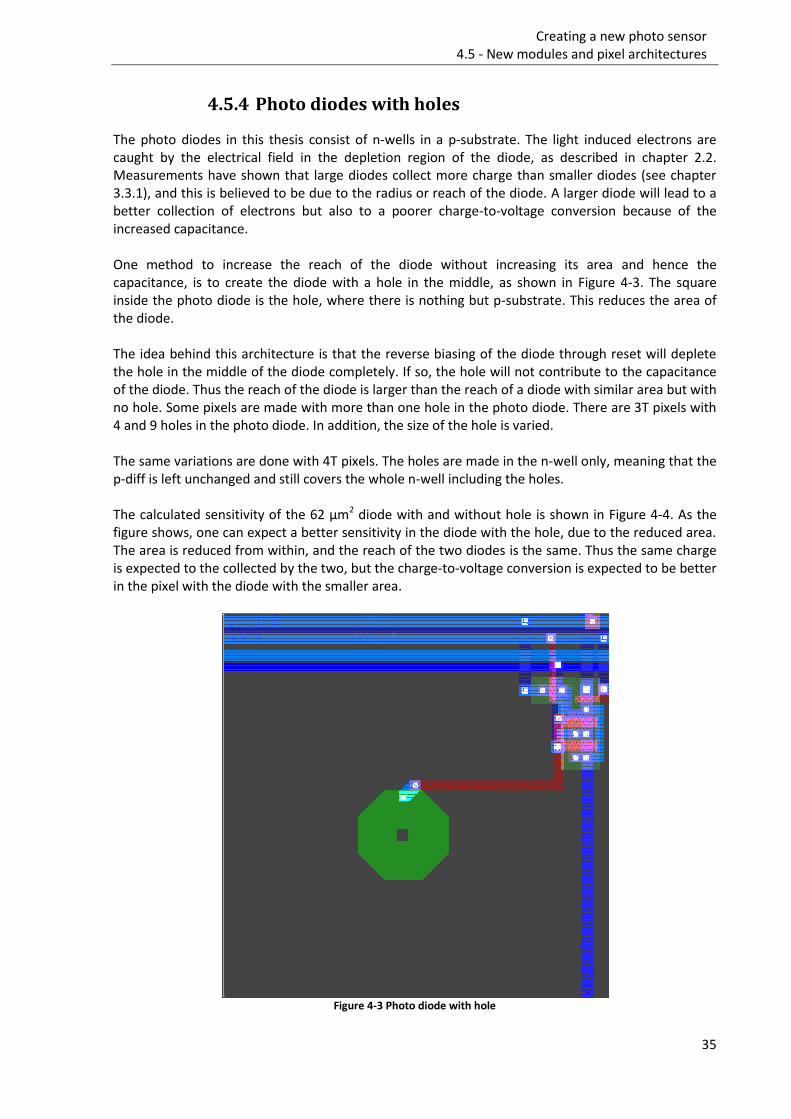
35
Creating a new photo sensor 4.5 - New modules and pixel architectures
4.5.4 Photo diodes with holes
The photo diodes in this thesis consist of n-wells in a p-substrate. The light induced electrons are caught by the electrical field in the depletion region of the diode, as described in chapter 2.2. Measurements have shown that large diodes collect more charge than smaller diodes (see chapter 3.3.1), and this is believed to be due to the radius or reach of the diode. A larger diode will lead to a better collection of electrons but also to a poorer charge-to-voltage conversion because of the increased capacitance. One method to increase the reach of the diode without increasing its area and hence the capacitance, is to create the diode with a hole in the middle, as shown in Figure 4-3. The square inside the photo diode is the hole, where there is nothing but p-substrate. This reduces the area of the diode. The idea behind this architecture is that the reverse biasing of the diode through reset will deplete the hole in the middle of the diode completely. If so, the hole will not contribute to the capacitance of the diode. Thus the reach of the diode is larger than the reach of a diode with similar area but with no hole. Some pixels are made with more than one hole in the photo diode. There are 3T pixels with 4 and 9 holes in the photo diode. In addition, the size of the hole is varied. The same variations are done with 4T pixels. The holes are made in the n-well only, meaning that the p-diff is left unchanged and still covers the whole n-well including the holes. The calculated sensitivity of the 62 µm2 diode with and without hole is shown in Figure 4-4. As the figure shows, one can expect a better sensitivity in the diode with the hole, due to the reduced area. The area is reduced from within, and the reach of the two diodes is the same. Thus the same charge is expected to the collected by the two, but the charge-to-voltage conversion is expected to be better in the pixel with the diode with the smaller area.
Figure 4-3 Photo diode with hole
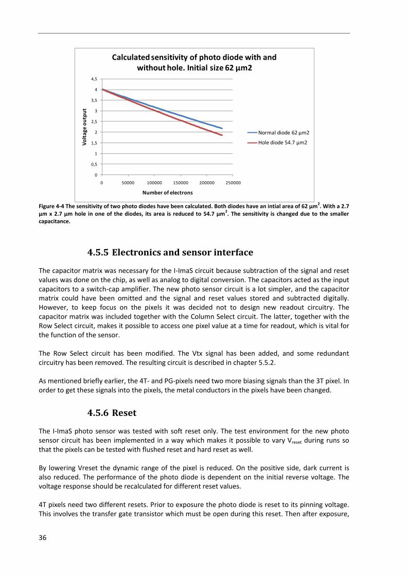
36
Figure 4-4 The sensitivity of two photo diodes have been calculated. Both diodes have an intial area of 62 µm
2. With a 2.7
µm x 2.7 µm hole in one of the diodes, its area is reduced to 54.7 µm2. The sensitivity is changed due to the smaller
capacitance.
4.5.5 Electronics and sensor interface
The capacitor matrix was necessary for the I-ImaS circuit because subtraction of the signal and reset values was done on the chip, as well as analog to digital conversion. The capacitors acted as the input capacitors to a switch-cap amplifier. The new photo sensor circuit is a lot simpler, and the capacitor matrix could have been omitted and the signal and reset values stored and subtracted digitally. However, to keep focus on the pixels it was decided not to design new readout circuitry. The capacitor matrix was included together with the Column Select circuit. The latter, together with the Row Select circuit, makes it possible to access one pixel value at a time for readout, which is vital for the function of the sensor. The Row Select circuit has been modified. The Vtx signal has been added, and some redundant circuitry has been removed. The resulting circuit is described in chapter 5.5.2. As mentioned briefly earlier, the 4T- and PG-pixels need two more biasing signals than the 3T pixel. In order to get these signals into the pixels, the metal conductors in the pixels have been changed.
4.5.6 Reset
The I-ImaS photo sensor was tested with soft reset only. The test environment for the new photo sensor circuit has been implemented in a way which makes it possible to vary Vreset during runs so that the pixels can be tested with flushed reset and hard reset as well. By lowering Vreset the dynamic range of the pixel is reduced. On the positive side, dark current is also reduced. The performance of the photo diode is dependent on the initial reverse voltage. The voltage response should be recalculated for different reset values. 4T pixels need two different resets. Prior to exposure the photo diode is reset to its pinning voltage. This involves the transfer gate transistor which must be open during this reset. Then after exposure,
0
0,5
1
1,5
2
2,5
3
3,5
4
4,5
0 50000 100000 150000 200000 250000
Vo
ltag
e o
utp
ut
Number of electrons
Calculated sensitivity of photo diode with and without hole. Initial size 62 µm2
Normal diode 62 µm2
Hole diode 54.7 µm2

37
Creating a new photo sensor 4.6 - Others’ contributions to the photo sensor
the FD is reset to the standard reset voltage (e.g. 5 V) before the collected charge is transferred. The transfer gate transistor is closed during this reset.
4.6 Others’ contributions to the photo sensor
Kjetil B. Stiansen has created the operational amplifier, as a part of the work for his master thesis. Joar Martin Østby has made the switching circuitry at the output of the circuit.

38
5 The new photo sensor
5.1 Introduction
In this chapter the new photo sensor circuit is described in detail. First an overview of the circuit is presented, then the pixel matrix and the pixels themselves are described. Finally the biasing circuitry is presented.
5.2 Overview of the circuit
Layout of the new photo sensor circuit is shown in Figure 5-1. The circuit is 3 mm x 3 mm = 9 mm2. The outermost square is the pad ring, where signals and biasing voltages and currents are fed into the circuit and results are read out. Biasing and timing diagrams are presented in chapter 6. The two large squares on the left inside the pad ring are pixel matrices, each consisting of 32x32 pixels. The two pixel matrices including biasing circuitry are equal. They have some switching circuitry on the output in common. In the following, only the bottommost part of the circuit is described. This part of the circuit is shown in Figure 5-2. Below the pixel matrix there is a biasing circuit called Row Select, described in more detail in chapter 5.5.2. This circuit makes it possible to select the pixels by the row for readout and for resetting them before exposure. In Figure 5-2 the pixel matrix is tilted 90o to the left, so that the rows are vertical, and the topmost row is on the left. The green rectangle in the middle of the pad ring in Figure 5-1 is four capacitor matrices, two of which are also shown in Figure 5-2. The pixels are read out one row at a time, and this means that 32 signal and reset values are stored on the capacitor matrix at a time. Then the signal and reset values are subtracted and read out sequentially. The capacitor matrix is described in chapter 5.5.3. On the bottom under the capacitor matrices is a small circuit called the Column Select, which controls which pixel value is to be sent from the capacitor storage to the output line. The Column Select is described in chapter 5.5.4. The current mirrors necessary to bias the source follower transistors in the pixels are hard to spot in the figure, but there are two of them, each with 16 current outputs. In Figure 5-2 they are shown as two pink rectangles between the pixel matrix and the capacitor matrix. The current mirrors are described in more detail in chapter 5.5.5. The small circuits on the upper right of Figure 5-2 are operational amplifiers (opamps) and some switching circuitry. The opamps are coupled as follower buffers, and through a switch on the

39
The new photo sensor 5.2 - Overview of the circuit
printboard the operator can choose whether to send the output values through these buffers or to read them out directly.
Figure 5-1 Layout of the photo sensor circuit. Inside the pad ring there are two similar photo sensor circuits. On the right there are three operational amplifiers, two of which are coupled to the photo sensor as output buffers.

40
Figure 5-2 The pixel matrix with its biasing and readout circuitry is repeated twice in the circuit. One of the circuits is
shown here. The 32x32 pixel matrix is the largest shape on the top left, and is tilted 90° to the left. The row biasing circuit
is on the bottom left, and the column biasing on the bottom right. On the right there are two identical capacitor matrices.
5.3 The pixel matrix
Each pixel is 32x32 µm. This is the same size as the I-ImaS pixels. The cancer registry of Norway states that a functional size for a mammography pixel is between 50 and 100 µm (3). This statement is dated in 2005. The acceptance of such a low spacial resolution is mainly the need for larger radiation doses when the pixels become smaller. The pixel size is chosen mainly because it fits the biasing circuitry from the I-ImaS circuit and because it simplifies comparison between the two circuits. The pixel matrix consists of 32x32 = 1024 pixels, as shown in Figure 5-3. There are 35 different pixel architectures. These are implemented in the bottom part of the matrix, seen as mostly grey in Figure 5-3, as opposed to the mostly blue pixels in the top part of the matrix. In the bottom part of the matrix, there are 16 pixels of each type, placed in 4x4 squares. The blue coloured pixels are partly covered with metal. They are described in chapters 5.4.3.9 and 5.4.3.10. In the bottom grey part of the pixel matrix in Figure 5-3, each pixel is repeated 16 times in a 4 x 4 square. In a normal image sensor, all pixels are identical. Each pixel is influenced by the architecture and light absorption of its neighbouring pixels, and the 4x4 square of identical pixels in the test matrix is to ensure that the four pixels in the middle of the square are surrounded by a uniform environment, resembling the environment of a pixel in a uniform image sensor. The pixels on the edges of the 4x4 squares are not guaranteed anything from their neighbours, so the results from these pixels are less reliable.

41
The new photo sensor 5.3 - The pixel matrix
Figure 5-3 Pixel matrix. There are 32 rows and 32 columns. The rows are counted from the top, and the columns are counted from right to left.
The pixel matrix is logically divided into rows and columns. In Figure 5-3 the topmost row is Row0, and the bottommost row is Row31. The columns are vertical, and counted from right to left, so that the rightmost column is Col0. The columns are divided into channels, with 16 columns in each channel. According to this, the rightmost 16 columns make Channel0, and the leftmost 16 columns make Channel 1. The two pixel matrices are logically separated by the numbering of channels, in that the second pixel matrix consists of Channel2 and Channel3. During readout, the rows are selected one by one. The column selector counts only 16 columns, and one column in each channel is selected for readout simultaneously. Thus, two pixels from each pixel matrix are sampled simultaneously, into its two capacitor matrices. The switching circuitry makes sure that the results from only one pixel are read out at a time. A simplified version of the part of the matrix with different pixel architectures is shown in Figure 5-4. Instead of 4x4 squares of each pixel, the pixels are shown only once, for a clearer view of the different pixel architectures. Table 5-1 displays the names of the corresponding pixel in Figure 5-4. The names of the pixels are explained in Table 5-2.

42
Figure 5-4 Pixel matrix simplified, showing the 35 different pixel architectures. The pixels with dark green photo diodes are 3T pixels. The 4T pixels are shown with yellow-green photo diodes. The red pixels are PG pixels.
pix_3T_2 pix_3T_10 pix_3T_25 pix_3T_46 pix_3T_62 pix_3T_98 pix_3T
_98_SF_w8
pix_3T _SFmin_d2
pix_3T _SFmin_d10
pix_3T _SFmin_d25
pix_3T _SFmin_d46
pix_3T _SFmin_d62
pix_3T _diff_SFmin
pix_3T _4diff_SFmi
n
pix_4T_46 pix_4T_62 pix_4T_98 pix_4T_132 pix_4T _132_u
pix_4T_208 pix_3T
_46_SF_w2
pix_PG _FD11
pix_PG_FD5 pix_4Th _62_4h0
pix_4Th _132_9h0
pix_3Th _46_h0
pix_3Th _46_h084
pix_2D _SFmin
pix_PG pix_PG _SFmin
pix_3Th _62_4h0
pix_3Th _132_9h0
pix_3Th _62_h0
pix_3Th_ 62_h084
pix_2D _SFstd
Table 5-1 Pixel names, corresponding to Figure 5-4.

43
The new photo sensor 5.4 - The pixels
5.4 The pixels
5.4.1 Overview
There are 35 different pixel architectures, described in short in Table 5-2. All pixel names start with the prefix “pix”, followed by an acronym describing the pixel type. 3T and 4T denote the 3-transistor and 4-transistor pixels, respectively, while PG denotes photo gate pixels. The 3Th and 4Th pixels have photo diodes with holes. The 2D pixel is a 3T pixel with two photo diodes. The following number denotes the area of the photo diode. The notion “SFmin” denotes a minimum sized source follower. The prefix “d” means diode area, and the prefix “h” means hole size relative to the minimum hole size of 1 µm2.
Pixel name Description
pix_3T_2 3T pixel with smallest diode, area = 2.4 µm2
pix_3T_10 Diode area = 10 µm2
pix_3T_25 Diode area = 25 µm2
pix_3T_46 Standard 3T pixel, diode area = 46 µm2
pix_3T_62 Diode area = 62 µm2
pix_3T_98 Diode area = 98 µm2
pix_3T_SFmin_d2 Smallest source follower, smallest diode
pix_3T_SFmin_d10 Smallest source follower, diode area = 10 µm2
pix_3T_SFmin_d25 Smallest source follower, diode area = 25 µm2
pix_3T_SFmin_d46 Smallest source follower, diode area = 46 µm2
pix_3T_SFmin_d62 Smallest source follower, diode area = 62 µm2
pix_3T_98_SF_w8 Source follower width 8 µm, diode area 98 µm2
pix_3T_46_SF_w2 Source follower width 2 µm
pix_4T_46 4T pixel, n-well diode area = 46 µm2
pix_4T_62 4T pixel, n-well d iode area = 62 µm2
pix_4T_98 4T pixel, n-well d iode area = 98 µm2
pix_4T_132 Standard 4T pixel, diode area = 132 µm2
pix_4T_132_u No guard bar around FD
pix_4T_208 Diode area = 208 µm2
pix_3Th_46_h0 Standard diode with small hole
pix_3Th_46_h084 Standard diode with large hole
pix_3Th_62_4h0 62 µm2 diode with 4 small holes
pix_3Th_62_h0 62 µm2 diode with 1 small hole
pix_3Th_62_h084 62 µm2 diode with 1 large hole
pix_3Th_132_9h0 132 µm2 diode with 9 small holes
pix_4Th_62_4h0 4T pixel with 4 holes in the n-well
pix_4Th_132_9h0 4T pixel with 9 holes in the n-well
pix_PG Standard photo gate pixel
pix_PG_FD11 Photo gate pixel, smaller FD
pix_PG_FD5 Photo gate pixel, smallest FD
pix_PG_SFmin Photo gate pixel with minimum SF
pix_2D_SFstd 3T pixel with two diodes
pix_2D_SFmin 3T pixel with two diodes and minimum SF
pix_3T_diff_SFmin 3T pixel with small n-diff photo diode
pix_3T_4diff_SFmin 3T pixel with 4 small n-diff photo diodes Table 5-2 Pixel names and descriptions

44
5.4.2 The electronics of the pixel
There are three nmos 5V-transistors in a 3T pixel, as shown in Figure 5-5. The standard sizes are shown in Table 5-3. The function of a 3T pixel is described in chapter 2.3.2.1. The schematics in this section are drawings. The actual schematics are shown in Appendix A.
Figure 5-5 A 3T pixel consists of three transistors and a photo diode.
Transistor Width Length Function
Reset transistor 1 µm 0.5 µm Resets the photo diode to reference reset voltage
Row select transistor 1 µm 0.5 µm Couples the pixel to the capacitor matrix
Source follower 4 µm 0.8 µm Current amplification of the diode voltage Table 5-3 Standard transistor sizes. The source follower is varied in some pixels.
The same basic electronics are used in the 4T and PG pixels. The schematics of a 4T pixel is shown in Figure 5-6. The new transistor (transfer transistor TX) is made up of the photo diode on the left, the floating diffusion (FD) on the right and a polysilicon gate. The buried photo diode is described in chapter 2.3.2.2. The photo gate pixel electronics is the same as for the 4T pixels. Schematics of a PG pixel is shown in Figure 5-7. The sensing node in the figure is made up of the photo gate (PG). The transfer transistor (TX) is made up of the floating diffusion (FD) on the right, and a small diffusion area on the left between the transistor gate and the photo gate.
PD
VDD
M3
M2
M1 Row Select
Vreset
Reset

45
The new photo sensor 5.4 - The pixels
Figure 5-6 A 4T pixel consists of four transistors and a complicated photo diode which is presented as two photo diodes.
Figure 5-7 A PG pixel consists of four transistors and a photo gate denoted as the sensing node.
5.4.3 Pixel architectures
5.4.3.1 The standard pixel
The pixel pix_3T_46 is denoted as the standard pixel. The name indicates that it is a 3-transistor pixel, the diode area is 46 µm2. The diode is octagonal, and the sides of the octagon are made as equal as possible, making an even octagon. Layout of the standard pixel is shown in Figure 5-8. All other pixel architectures are based on this pixel. The other pixels with the same naming structure (pix_3T_x) are in the same category, and only the size of the diode changes between these pixels. The number indicates the area of the diode. There are six pixels in this category, the diode sizes varying from 2 to 98 µm2. These pixels can be seen in the top row of Figure 5-4 and Table 5-1. These pixels are expected to vary in sensitivity.
FD
VDD
Vtx Vpg
PG
M4
TX M3
M2
M1 Row Select
Vreset
Reset
VDD
TX
PD
FD
M4
Vtx
M3
M2
M1 Row Select
Vreset
Reset

46
Figure 5-8 The standard pixel. The green octagon is the photo diode. The blue lines are metal conductors. On the top right is the electronics. The two fingered transistor (poly in pink) is the source follower, and the other two transistors are the reset transistor and the Row Select transistor.
5.4.3.2 3T_SFmin
The name of these pixels indicates that the source follower SF is at minimum size, i.e. W=0.4 µm, L=0.5 µm. Apart from the change in source follower size, these pixels are identical to the pix_3T_x. There are five of these pixels, corresponding to the five of the pix_3T_x with the smallest photo diodes. These pixels are denoted pix_3T_SFmin_dx, and can be seen in the second row of Figure 5-4 and Table. These pixels are implemented in order to see how the gate capacitance of the source follower affects the charge-to-voltage conversion of the pixel.
5.4.3.3 Other variations of the 3T pixel
To further investigate the influence of the source follower gate capacitance, the standard pixel has been implemented with a third SF size, W=2 µm, L=0.8 µm. This pixel is named pix_3T_46_SF_w2, indicating that the SF width is 2 µm. This pixel is the one most identical to the most sensitive pixel in the I-ImaS test structure. The pixel most identical to the I-ImaS standard pixel is pix_3T_98_SF_w8. The name indicates that the source follower width is 8 µm, twice the width of the standard pixel SF. This pixel has been implemented in order to compare the two circuits to the I-ImaS standard pixel.
5.4.3.4 4T pixels
As mentioned earlier, 4T pixels are documented to be better suited than 3T pixels for low light applications. It is therefore interesting to compare these pixel architectures. When implemented on the same chip, conditions are optimal for comparing the two. 4T pixels in general are described in chapter 2.3.2.2. The layout of the standard 4T pixel is shown in Figure 5-9.The standard 4T pixel has a photo diode larger than the standard 3T pixel. The n-well photo diode size is 132 µm2, a diode size which also exists in the 3T pixels. The 4T pixels have the same initial architecture as the 3T pixels. In addition comes the diode made up of the n-well and the p-diffusion. The reset transistor, the SF and the row select transistor are the same as for the 3T

47
The new photo sensor 5.4 - The pixels
pixels. The photo diode is buried, as shown in Figure 5-10. (Buried diodes are described in chapter 2.3.2.2.) The pixels also have a floating diffusion FD implemented as an n-diffusion. The standard FD size is 17.4 µm2 and has been calculated from equation [5] on page 9. According to the calculations FD is capable of holding the charge from 200.000 electrons. FD is protected by a guard bar implemented as a p-diffusion ‘fence’ connected to ground. FD is situated beneath the metal conductors in the pixels, so that they occupy as little of the sensitive part of the pixel as possible. The fill factor is nevertheless a little reduced, mainly because of the guard bar around the FD. The pixels in this category have varying diode sizes. There are six pixels in this category, with five different diode sizes. The n-well diode sizes vary from 46 to 208 µm2. The pixels are named pix_4T_x, and the pixel pix_4T_132_u is equal to the standard 4T pixel pix_4T_132, but without the guard bar around FD. The sizes of the photo diodes are larger than for the 3T pixels because of the charge transfer to FD as explained in chapter 2.3.2.2. There is also a 4T pixel with the same n-well diode size as the standard 3T pixel, 46 µm2.
Figure 5-9 The standard 4-transistor pixel. The nwell (green) is mostly covered with p-diffusion, shown as a brown/pink shape. The floating diffusion is shown in the top middle, where both the guard bar and the transfer gate are shown as pink shapes.
Figure 5-10 The buried photo diode seen from the side. The n-well is mostly covered by a p-diffusion.
n-well n-well
p-diff
Buried diode Normal diode
p-substrate

48
5.4.3.5 Photo gate pixels
Just like 4T pixels, PG pixels are more sensitive to low light than 3T pixels, according to the literature. Thus, these have been implemented for the same reasons. The photo gate pixels have the same electronics as the 4T pixels, including the FD, but without the guard bars. Layout of a photo gate pixel is shown in Figure 5-11, and the schematics are repeated in Figure 5-12 for illustration. What separates the photo gate pixels from the other pixels is the absence of a photo diode. Instead these pixels have a polysilicon gate covering most of the sensitive area, as described in chapter 2.3.2.3. Two attributes are varied in the photo gate pixels, the floating diffusion and the source follower. The pixels in this category are pix_PG, pix_PG_FD11, pix_PG_FD5 and pix_PG_SFmin. In pix_PG_FD11 the floating diffusion is 11 µm2, and in pix_PG_FD5 the floating diffusion is 5 µm2. In the other PG pixels, the floating diffusion is the standard size 17.4 µm2. The standard size floating diffusion has been calculated to be the optimal size for collecting 200.000 electrons. Thus, the smaller FDs (in theory) are too small for this purpose. However it is interesting to document the difference in sensitivity for the different architectures for two reasons. First the mammography technology is constantly developing, and the radiation doses may change. Second it is uncertain whether the photo gate is able to collect all the electrons and have them transferred to the FD. If not, there is no need for a full size floating diffusion.
Figure 5-11 Photo gate pixel. The large red shape is the polysilicon gate, shown as PG in Figure 5-12. The floating diffusion is shown as a purple rectangle above the photo gate (FD in Figure 5-12).

49
The new photo sensor 5.4 - The pixels
Figure 5-12 Schematics of the photo gate pixel is repeated here for illustration
5.4.3.6 Diodes with holes
The voltage output of the pixel is restricted by the capacitance in the sensing node according to the charge-to-voltage conversion function V=Q/C. The capacitance is a weighted sum of the area and perimeter of the photo diode, while the collection of electrons is believed to depend more on the radius of the diode. In theory there is a way to reduce the area of the n-well diode without reducing the radius and the reach of the diode. This can be done by creating holes in the n-well diode and making sure that the holes are depleted during exposure. Depletion is important to avoid increased sidewall capacitance caused by the hole. The layout of such a pixel is shown in Figure 5-13.
Figure 5-13 Diode with hole
FD
VDD
Vtx Vpg
PG
M4
TX M3
M2
M1 Row Select
Vreset
Reset

50
Creating the hole is straightforward, cutting a hole in the layout of the n-well. Making sure the hole is depleted is a different matter, in that voltage dependent junction depth is not disclosed by the manufacturer. However, most of these pixels have been made with the minimum hole size 1 µm x 1 µm, which is believed to be small enough to be constantly depleted. The larger holes are 2.7 µm x 2.7 µm. There are eight different pixels with holes, seen in the two bottom rows in Figure 5-4. Both 3T and 4T pixels are implemented this way. Where there are more than one hole, the spacing between the holes is the minimum spacing, 1.7 µm. The pixels with holes are denoted 3Th and 4Th, and are described in Table 5-2. There are pixels equal to all of these only without the holes, for comparison.
5.4.3.7 Diff-diode pixels, 3T
Two of the 3T pixels have tiny diodes, implemented in n-diffusion. Both these pixels have a minimum size source follower, to keep the SF gate capacitance small relatively to the small diode capacitance. The diffusion diodes are square, 1.44 µm2. The two pixels are pix_3T_diff_SFmin and pix_3T_4diff_SFmin, where the latter name indicates that there are four diodes in the pixel. These pixels are interesting with respect to their sensitivity, but are thought to be unable to collect the maximum amount of electrons. The diff-diode pixels were more or less copied from the I-ImaS test pixels because there was not enough time to test them during the I-ImaS testing. Calculations and ideas behind these pixel architectures are I-ImaS confidentials.
5.4.3.8 Pixels with two n-well diodes
The two-diode (2d) pixels, shown in Figure 5-14, have the same electronics as the 3T pixels. There are two photo diodes in each pixel, size 26 µm2. There are two such pixels, with standard SF and minimum SF. These are included on the same basis as the diff-diode pixels. These pixels are interesting with respect to charge collection, because the photo diodes are not centred in the pixel.
Figure 5-14 Pixel with two photo diodes

51
The new photo sensor 5.4 - The pixels
5.4.3.9 Pixels covered with metal
Light induced electrons diffuse across the wafer until they recombine with holes, or are caught by a photo diode or some other trap in the electronics. Some of these electrons might diffuse to a neighbouring pixel and be collected by the photo diode there. Some of the photons might also be reflected by the metal in a pixel so that it changes direction and is absorbed by a neighbouring pixel. This is denoted as neighbour influence. A part of the pixel matrix has been made with the standard pixel architecture and varying metal covering to study this phenomenon. This part is seen in Figure 5-3 as the blue shape, the six rightmost columns excluded. Some of the pixels are covered with metal, to prevent any light from hitting them directly, see Figure 5-15. The metal covered pixels have different numbers of metal covered neighbours, so that the influence can be measured as a function of the number of uncovered neighbours. Any non-zero output from these pixels must be due to neighbour influence, and the output is expected to increase as the number of uncovered neighbours increases. The metal covering is implemented in metal2. The most optimal would be to implement it in metal1, because it is the metal layer closest to the wafer. However metal1 is used in the routing between the photo diode and the poly conductor. Thus covering the pixel with metal1 would contribute to the capacitance of the diode. Alternatively a hole could be made in the metal covering to avoid the small piece of metal1 in the diode. But this would let light into the diode. To avoid this problem, the metal covering was implemented in metal2. Since all four metals are used to bias the pixels, it is impossible to cover the pixels totally without causing a short circuit. The pixels are therefore covered by as much metal as possible within these restraints. The outputs from these pixels should therefore not be compared to the dark response of the standard pixel, but to the response of a metal covered pixel with only metal covered neighbours exposed to the same amount of light. The influence between pixels will affect the sharpness (acutance) in the resulting image. This is why it is important to document the amount of neighbour influence. If the influence is large, steps might be taken to reduce it. A large neighbour influence may also contribute to the maximum amount of electrons collected by a pixel. This will in turn lead to the need for larger photo diodes in order to collect all the neighbour induced charge.
Figure 5-15 Pixel covered with metal. The metal covering is implemented in metal2.
The pixel is not totally covered because metal2 is used in the electronics as well. Metal2 is shown as dark blue.

52
5.4.3.10 Pixels partly covered with metal
The sensitivity of different parts of the pixel with respect to distance from the photo diode is up for testing. Together with information about neighbour influence, results from this testing can indicate whether the size of the pixel is optimal. Too small pixels will yield large neighbour influence, while too large pixels will be unable to collect charge induced in peripheral parts of the pixel. Results from testing the I-ImaS circuit showed that there was a neighbour influence of 10 %, which indicates that the photo diodes are able to collect electrons from neighbouring pixels to a relatively large extent. This indicates that the pixels are not too large. Larger pixels could perhaps reduce the neighbour influence, but it would also have other, possibly negative, consequences. In order to do some further research on the areas from which the photo diode collects electrons, some pixels are implemented with metal covering which lets light into certain areas of the pixel. In Figure 5-3 these pixels are implemented in the rightmost part of the top blue shape. They are all implemented as the standard pixel. The pixels are covered with metal, and then some of the metal has been removed, so that there is a metalless ring, as shown in Figure 5-16. There are six different implementations, repeated twice, with the uncovered ring in different distances from the photo diode. The neighbours of these pixels are covered with metal, as described in the previous section, so that the pixels in focus are exposed to minimal neighbour influence. The partial metal covering is copied from the I-ImaS test pixels, to make them comparable.
Figure 5-16 Pixel partly covered with metal. The octagonal grey shape is the uncovered part of the pixel. The other grey
areas are uncovered because the metal is also used in the electronics of the pixel, as explained in chapter 5.4.3.9.

53
The new photo sensor 5.5 - Biasing and readout
5.5 Biasing and readout
5.5.1 The path of the signal
The creation of the signal and reset voltages in the pixel is described chapter 2. From the sensing node, the signal voltage is amplified through the source follower amplifier consisting of the amplifier transistor in the pixel and a current mirror. There is no voltage amplification, but current amplification makes the signal able to travel a distance through the pixel matrix into the storage matrix. One row of pixels is read out to the storage matrix at a time, which means that 64 values are stored from one pixel matrix, i.e. the signal and reset values. From the storage matrix the values are given access to two double readout lines so that two signal and reset values are read out from the capacitor matrix at a time. Finally two 4 to 1 multiplexers put the voltages on the double output line, one for signal values and one for reset values. (4:1 because there are two similar pixel matrices, and all in all four double readout lines from the storage matrices.) On the output line behind the multiplexers, there are two follower coupled opamps, and a new set of multiplexers controls whether the signal is sent through this buffer or put directly out of the circuit. The path between the storage matrix and the output is shown in Figure 5-17.
Figure 5-17 The path of the signal between the capacitor matrix and the output. There are two pixel matrices, each with two channels and two capacitor matrices. All in all, four signal values and four reset values are read out from the capacitor matrices at a time. Two 4:1 multiplexers choose between these so that one signal and reset value is read out of the circuit at a time. The second set of multiplexers decide whether the values are buffered or not.

54
5.5.2 The Row Select circuit
Figure 5-18 The Row Select circuit selects the pixels by the row. The connection of pixels to the capacitor matrix is controlled from here. The Row Select circuit also manages the transfer gate signal and the reset of the pixels.
The Row Select circuit controls three bias signals, the row select signal (RS) itself, the transfer gate signal (VTX) and the reset signal (ResetA in Figure 5-18). Figure 5-18 shows a small part of the circuit, biasing one row of pixels. RS connects the pixels in one row to the capacitor matrix, and switching in the capacitor matrix makes it possible to store both signal and reset values. The VTX signal is used in the 4T pixels and PG pixels to transfer the accumulated charge from the sensing node to the floating diffusion for readout. The ResetA signal corresponds to the Reset signal in the pixels, and couples the photo diodes and floating diffusions (FD) to the Reset voltage supply. The digital signal circuits use 3.3 V logic, while the electronics in the pixels make use of 5 V logic. The inverting steps in the middle of Figure 5-18 carries out the transformation between the two. The whole Row select circuit is made up of 32 equal parts as shown in Figure 5-18. They are connected via flip-flops which create a shift register. The RS_x signal goes high when a road is to be selected for readout, the Vtx_x signal determines if the 4T and PG pixels in a road are to transfer the accumulated charge to the FD for readout, and when the Reset_x signal goes high, the selected row of pixels is reset. The Q signal from the flip-flop controls which row of pixels receives these signals.

55
The new photo sensor 5.5 - Biasing and readout
5.5.3 Capacitor matrix – analog storage
Figure 5-19 Part of capacitor matrix. The Vin node is connected to one pixel at a time. The signal and reset values are stored on separate capacitors C1 and C2, controlled by switches W2 and W3.
The capacitor matrix consists of 16 pairs of capacitors for storage of signal and reset voltages. There are two capacitor matrices per pixel matrix, one for each channel of pixels. A small part of the capacitor matrix, showing one pair of capacitors, is given in a simplified version in Figure 5-19. The actual schematics are shown in Appendix A. When one row is selected for readout, the entire row of pixels is read out simultaneously, to 32 pairs of capacitors (two capacitor matrices). The signal value from one pixel is stored on one capacitor, and the reset value on the other. The part of the circuit shown in Figure 5-19 shows the storage elements for one column in the pixel matrix. The voltage on the output from the pixel is presented on Vin. The signals Sample_signal and Sample_reset control the switches W2 and W3 so that the signal and reset values are stored on separate capacitors. The further readout is done sequentially, controlled by the Column Select circuit, controlling the readout switches W4 and W5 shown in Figure 5-19. The Signal_Out and Reset_Out lines are connected to common readout buses. Since there are all in all four of these readout buses in the circuit, there is some switching between them before the signals can be read out from the circuit. The CSC-signal controls the switch between the storing capacitors, which closes when the values are to be read out, so that the differential value is presented on the output.

56
5.5.4 The Column Select circuit
Figure 5-20 Part of the Column select circuit
The Column Select circuit is a simple digital circuit which creates the signal that controls W4 and W5 in Figure 5-19, selecting one pair of capacitors, containing the signal and reset values from one pixel. The circuit is built up of flip-flops and logic gates, see Figure 5-20. 16 of these circuits are connected via the flip-flops creating a shift register. Two capacitor matrices are biased from one Column Select circuit so that two signal and reset values are read out from the capacitor matrix simultaneously. The CS_x signal indicates that a column is to be selected, and Q decides which column to select.
5.5.5 Current mirror
Figure 5-21 Current mirror, detail

57
The new photo sensor 5.5 - Biasing and readout
The source followers in the pixels need a current source. This is provided by a current mirror. A detailed part of the current mirror is shown in Figure 5-21 for illustration. The schematics of the whole current mirror is shown in Appendix A. This is the simplest form of current mirror, copying the current IB to the outputs IB_COL_x. The bias current IB is mirrored 16 times, two of which are shown in the figure. The row select circuit makes sure that only one row of pixels is connected to the output at any time. The current drawn from one column will then in effect be drawn from one pixel and thus the source follower is complete. There are two current mirrors, each serving one channel.

58
6 Testing
6.1 Data Acquisition
Figure 6-1 The test bench at the laboratory. On the left is the digital analyzer. The computer in the middle is the LabView computer. In the cardboard box to the right are the PCBs and the photo sensor circuit. On the shelf there are two power supplies. The photo is taken during testing of the digital signals.
The photo sensor is implemented on a chip measuring 3 mm x 3 mm. It has been bonded to a 68 pin package. The package has been mounted on a printed circuit board (PCB), where the power, biasing and signal lines are routed out to pins and contacts. 18 digital signals are needed to operate the photo sensor. In addition, some power and analog current and voltage biasing is necessary. The digital signals are provided by an FPGA. Analog and digital power is provided by a standard power supply, while biasing voltages and currents are provided by a LabView computer. The output voltages are fed into the LabView computer for analog to digital conversion and further processing and visualisation of the results. Some of the hardware used to test the photo sensor is listed in Table 6-1. The modules from National Instruments are put into the LabView computer. In addition there are some small IC packages and

59
Testing 6.1 - Data Acquisition
PCBs, as well as the power supplies. Photos of the test environment are shown in figures Figure 6-1, Figure 6-2 and Figure 6-3. Schematics and layout of the custom made PCB are shown in Appendix B.
Figure 6-2 The PCBs and the photo sensor circuit. On the left is the custom made PCB with the photo sensor circuit. The sensor is covered by a lid with a white sticker. The grey cables are connected to the digital analyzer for debugging. The two PCBs on the right (one mounted on top of the other) contain the FPGA which controls the digital biasing signals to the photo sensor.
Figure 6-3 The custom made PCB with the photo sensor circuit in the middle. The three BNC contacts on the bottom left are the output signal contacts and the trigger contact.

60
In this chapter the words “runs” and “frames” are used. The word “frame” refers to one round of reset, exposure and readout of the sensor. There may be several frames in one run, but within one run all biasing is held constant. The initial test bench software was made simple with one frame per run and manual trigging for each run. When the initial testing is ok and results look good, the plan is to expand the test bench to make it possible to run more frames and calculate average values and standard deviations, among other things.
Hardware description Manufacturer Model
PCB, custom made
Analog output National Instruments NI 6707
Digitizer National Instruments NI 5122
FPGA card Memec Design Spartan 3 LC
FPGA header card Memec Design P160 Table 6-1 Data Acquisition hardware

61
Testing 6.2 - Biasing
6.2 Biasing
To operate the circuit, several digital signals are required, in addition to power and biasing voltages and currents. The signals are listed in Table 6-2. Digital signal type Receiver of the signal Description D_CS DI Column shift.reg. D signal for flip-flop CLK_CS DI Column shift.reg. CLK signal for flip-flop RN_CS DI Column shift.reg. Reset of flip-flop D_RS DI Row shift.reg. D signal for flip-flop CLK_RS DI Row shift.reg. CLK signal for flip-flop RN_RS DI Row shift.reg. Reset of flip-flop RS_x DI Row_Select Select row of pixels for sampling Reset_x DI Row_Select Reset row of pixels Vtx_x DI Row_Select Transfer charge to floating diffusion C2 DI Output opamp Whether to use output buffer or not C0 DI Output switch Switching between capacitor matrix output lines C1 DI Output switch “” CSC DI Capacitor matrix Closing switch between storage capacitors Sample_signal DI Capacitor matrix Store pixel output on ‘signal capacitor’ Sample_reset DI Capacitor matrix Store pixel output on ‘reset capacitor’ CS_x DI Col_select – cap.matrix Putting stored values from one column on the
capacitor matrix output line LED_on DI LED LED switch Set_VM DI External switch Puts analog voltage on output pad (M1, M2) VCC5V PI Pixels Analog power 5 V VSS PI Digital circuitry Digital ground VDD PI Digital circuitry Digital power 3.3 V VDD3ALLP PI Pad ring Pad ring power 3.3 V GND3ALLP PI Pad ring Pad ring ground AVSS PI Pixels Analog ground AVCC_5V PI Digital circuitry Digital power 5 V IB1 C Pixels, source follower Bias current IB2 C Pixels, source follower “” IB3 C Pixels, source follower “” IB4 C Pixels, source follower “” Vreset AI/PI Pixels Pixel reset voltage supply VPG AI Pixels Biasing of the photo gate Reset_default AI Row_select - pixels Low potential of the reset transistor gate Reset_pulse AI Row_select – pixels High potential of the reset transistor gate Vtx_default AI Row_select – pixels Low potential of the transfer gate Vtx_pulse AI Row_select – pixels High potential of the transfer gate VM AI Output lines Biasing of the capacitor matrix M2 AO Output, signal values M1 AO Output, reset values
Table 6-2 Biasing. Digital input signals (DI) , power (PI), currents (C), analog voltage inputs (AI), analog voltage output (AO).

62
6.2.1 Analog biasing
6.2.1.1 Vreset
When Reset is high, the photo diode is coupled through the reset transistor to Vreset, which with soft reset is 5V. Vreset is coupled so that it is possible to change the voltage both between and during runs. This makes it possible to test the circuit with soft, hard and flush reset. With flush reset Vreset changes from a low to a high voltage during reset.
6.2.1.2 VM
The VM signal was added during testing of the circuit when it was discovered that the capacitor matrix was not biased correctly. VM functions as a virtual ground for the storage capacitors during sampling. The details about the VM signal are presented in chapter 7.3.1.
6.2.1.3 VPG
The photo gate pixels draw light induced electrons to the surface by adding a positive voltage VPG to the photo gate. The performance of the pixel varies with variations in VPG. According to the literature, low VPG voltages (e.g. slightly above 0 V)are good for the sensitivity of the pixel, while higher VPG voltages (e.g. 3 V) give better dynamic range (27).
6.2.1.4 IB
The source follower amplifiers in the pixels are not complete without a current source. This is fed to the pixel through the current mirrors. The bias current for the current mirrors is delivered by the LabView computer. The default bias current is 25 µA.
6.2.1.5 VTX and the pinning voltage
The pinning voltage of the 4T pixels is fed to the buried diode through the transfer gate transistor. Thus Vreset, the voltage fed to the gate of the transistor and the reset time all contribute to the final voltage over the buried diode.
6.2.2 Timing – digital biasing
There are essentially three procedures happening in sequence during testing. Before exposure, the pixels and shift registers need to be reset (global reset procedure). Then there is the exposure, during which the photo sensor is exposed to light. After exposure it is time for readout. Detailed timing diagrams can be found in Appendix C. The timing is different for 3T and 4T pixels, as explained in chapter 2.3.2.2. Therefore only one type of pixels can be tested at a time. During global reset, if 3T pixels are to be tested, the photo diodes are reset according to the reset type used after exposure. If the pixel is going to be reset with hard reset at 4 V, the global reset of the pixels is also 4 V. 4T pixels need two different types of reset, as described in chapter 4.5.6.

63
Testing 6.3 - Exposure
6.3 Exposure
The photo sensor is to be tested with a light emitting diode (LED). The intensity of the emitted light is determined by the current through the LED, which can be controlled. The exposure time is also controlled, so the total amount of light can be decided. The LED is the same as the one used in the I-ImaS project. Some key features are listed in Table 6-3. The green LED was chosen because it emulates the scintillator of choice (the CsI(TI) scintillator described in chapter 2.1.2). Light absorption in the silicon wafer with respect to depth is shown for several wavelengths in Figure 6-4. The topmost area of the wafer, to the left of the first vertical dashed line in Figure 6-4, absorbs mostly blue light. The middle area down to 1.5 µm absorbs mostly green light, and deeper down red light is best absorbed. The junction depth of the n-well diodes in the pixels is 2.0 µm, and as the figure shows, wavelengths at about 550 µm (green) are absorbed well at this depth, although it is more common to collect electrons induced from red light at this depth(13).
Manufacturer Philips Lumileds Lighting Company
Model Luxeon Emitter
Colour Green
Wavelength 520-550 nm, typically 530 nm.
Forward voltage 2.70 V – 3.99 V, typically 3.42 V
DC forward current Ca 100 mA - 350 mA Table 6-3 LED specifications
Figure 6-4 Absorption depth in silicon for various wavelengths (28). The areas separated by vertical dashed lines indicate
the depths at which it is optimal to measure blue, green and red light respectively.

64
6.4 Readout
The double output line from the circuit is connected via two BNC contacts on the PCB to the digitizer in the LabView computer. The two values are read out simultaneously by a sample-and-hold circuit in the digitizer. The output values are kept on the line for 1 µs before they are sampled. This is because of the unknown time constant of the contacts and cables.
6.5 Test runs
This section describes how the new photo sensor is to be tested. Unless otherwise is stated, the tests are to be performed on all types of pixels. This means that two different runs have to be done, one for 3T and one for 4T and PG pixels, with everything else held constant. These runs are denoted as 3T and 4T runs. Optimal usage of the LED is assumed, so that the linear range of the LED corresponds to the linear output range of the pixels. This can be achieved through calibration and pulse width modulation of the LED. Most of these tests have not been performed due to problems with the initial test. However, the tests are described the way they were meant to be done. The descriptions are also meant to be a guide to whoever might continue the work on testing the circuit.
6.5.1 Does everything work?
The first test is to couple everything together and run two frames with different light exposure to look at the result. Light differences can be made by switching off all lights in the room and then add some light for the second run. This initial testing is done with 3T runs. The outputs are expected to vary with varying light intensity. Furthermore, differences between different pixel architectures are expected, especially between 3T and 4T/PG pixels because the 4T pixels are not tested appropriately. What is read out from the 4T pixels during 3T runs is the collected charge in the floating diffusion. Also differences are expected in the area where some pixels are totally covered with metal while others are uncovered.
6.5.2 Calibration of the pixels
When the initial testing is done, it is time to attach the LED. The LED will need to be calibrated and adjusted in order to give a linear response in the sensitivity range of the pixels. When this is done, the pixels can be calibrated. During calibration, standard settings are used with respect to exposure time, reset values, IB etc. The brightness of the LED is stepped from very low to above the saturation points of the pixels, and noise floor and saturation points for all pixels are recorded. The actual amount of photons hitting the pixels during this testing is unknown, but some calculations have been done, and the results from this testing are to be compared to the calculations.
6.5.3 Pixel response
The LED brightness is stepped from the noise floor to the saturation point, and there are many frames per run. This way the average output values and standard deviations of the pixels can be calculated for each brightness step. Variations in one pixel between frames are expected, and say something about the noise level.

65
Testing 6.5 - Test runs
The average output values are expected to increase with increasing light intensity. Pixels with small photo diode are expected to saturate at lower light intensities than pixels with larger photo diodes. The noise floor of 4T and PG pixels may vary from that of 3T pixels because of the extra electronics and the processing of the signal within the pixels. Between the noise floor and saturation point, the pixel responses are supposed to be linear. The sensitivity of the pixels can be tested by comparing the output voltage of the pixels somewhere in the middle of the linear output range of the pixels. This will only be valid for pixels with similar noise floors. If the noise floors vary a lot, this must be compensated for. Alternatively, 4T pixels can be compared only to other 4T pixels. Comparison between 3T and 4T pixels can still be done based on these and other results.
6.5.4 Image lag
In the pixel response test the brightness of the LED is stepped between runs, and for each step many frames are taken. Since all frames in a run are done with the same brightness, the reset values from the previous frame vary very little. This reset value is the initial value for the next exposure. Image lag is tested by performing the pixel response test with a twist. Instead of many frames with the same light exposure in a row, the brightness is varied between all frames. Still the results from frames with the same brightness are added to calculate the average outputs and standard deviations. This way, different reset values from the previous exposures affect the signal values from the present exposure. Average values are expected not to differ from the pixel response test. This is true when the pixels are in the middle of the linear range. At low brightness, averages are expected to diverge more from those from the pixel response test, because previous exposures are mostly brighter than the present exposure. The same effect is expected with results from high brightness. The standard deviations are also expected to be larger because of the non-uniform initial values. The average values and standard deviations from this test, compared to those from the pixel response test will say something about the image lag in the pixels.
6.5.5 Reset
Pixel response and image lag is to be tested for all three types of reset. With hard reset, Vreset is lower than with soft reset. Vreset must be lower than the Reset signal voltage on the reset transistor gate, minus the gate-source threshold voltage of the transistor. Thus the optimal Vreset voltage for hard reset is believed to be around 4.2 V. Pixel response and image lag from a few pixels should be tested with different Vreset voltages in order to find one or two values for testing of all the pixels. Image lag is expected to be smaller with hard reset than with soft reset, but the dynamic range also shrinks. With flush reset, Vreset is first held at a low voltage before it is switched to the actual reset voltage (e.g. 5 V). During calibration a few pixels should be tested with respect to image lag with the initial low reset voltage varying with respect to voltage value and duration. Flush reset is expected to diminish the image lag.

66
6.5.6 Bias current
Testing of the I-ImaS circuit revealed that variations of the bias current had little effect on the performance of the sensor with respect to sensitivity and noise. The dynamic range was not tested with respect to bias current, however, and as mentioned in chapter 4.5.2, the voltage over the current mirror adds to the saturation voltage of the source follower transistor. This test is initiated by measuring the voltage over the current mirror directly with a voltmeter. If there is a significant voltage variation, the outputs are recorded with respect to bias current. If the voltage over the current mirror changes significantly with varying bias current, the dynamic range of the pixels are to be tested with the most promising bias current. Then, if the dynamic range has improved, the other tests must be run again with the new bias current.
6.5.7 Pinning voltage – 4T pixels
To calculate the pinning voltage, information about doping concentrations is needed. This is not disclosed by the manufacturer. To find the most optimal reset voltage for the 4T pixels, the reset voltage Vreset is to be varied while the transfer gate is kept open during reset of the diode. For each step, a few 4T pixels are tested with respect to dynamic range, linearity and sensitivity. When the most optimal reset voltage has been found, conclusions must be made as to whether the 4T pixels can compete with the 3T pixels. If so, the 4T pixels are to be tested the same way as the 3T pixels. If not, further research is required, and improved versions of the 4T pixels need to be implemented.
6.5.8 Photo gate voltage VPG
The photo gate (PG) pixels need to be calibrated with respect to the photo gate voltage VPG. As mentioned earlier, a low voltage is good for the sensitivity of the pixel, while a high voltage gives a better dynamic range. Thus, VPG must be stepped, and a few PG pixels tested for dynamic range. The dynamic range of the PG pixels can be compared to that of the standard 3T pixel. The standard 3T pixel has a calculated sensitivity range which is close to optimal for mammography calculations. The PG pixels therefore need to be sensitive over the same range. The VPG of choice is the one which gives the best sensitivity, while at the same time keeping full dynamic range. When this voltage is found, the PG pixels are to be tested the same way as the 3T pixels.
6.5.9 Different light sources.
The pixels are tested with a green LED because this emulates the most widely used scintillator. The n-well depth of 2.0 µm is more commonly used for detecting red light, however, and it would be interesting to see how the circuit responds to red light. The n-diff pixels, 4T pixels and PG pixels might respond better to blue light because they collect charge close to the surface.

67
Testing 6.6 - Comparisons between pixels
6.6 Comparisons between pixels
When the test runs are done, it is time to analyze the test results.
6.6.1 Dynamic range
Noise floor and saturation point is measured for all pixels. Measured saturation points are to be compared to the saturations points calculated for 3T pixels. Between the noise floor and the saturation points the output values of the pixels are expected to be close to linear with respect to the brightness of the LED. The noise floor is expected not to vary much between pixels. Variations in noise floor must be compensated for when measuring the pixel sensitivity.
6.6.2 Diode size, sensitivity
The 3T pixels are to be compared with respect to diode size, and so are the 4T pixels. The standard pixel is to be compared to the equivalent pixel from the I-ImaS test pixels. This is the pixel with the -2 diode and source follower width 2 µm, denoted as pixel 9 in Figure 3-5. Similarly pix_3T_98_SF_w8 is to be compared to the I-ImaS standard pixel. The I-ImaS pixels are expected to yield better results, because of the better fill factor.
6.6.3 Source follower size
Some pixels have been implemented with varying source follower size. These are to be tested with respect to sensitivity and dynamic range. The results from testing the I-ImaS circuit indicate that small source followers are more optimal for the pixels than large ones. It is also interesting to see whether the bias current IB influences on these results.
6.6.4 Influence between pixels
Influence between pixels is to be tested the same way as it was tested in the I-ImaS project. Since the pixels in the new photo sensor circuit are not totally covered with metal, as described in chapter 5.4.3.9, the zero value must be defined differently. This is because some light is expected to hit the covered pixels through the holes in the metal. One solution is to denote the output value from a covered pixel with covered neighbours – exposed to the same light as the rest of the pixels - as the zero value. Because of the issue of the zero value, comparing these results with those from the I-ImaS test pixels might be difficult.
6.6.5 Fixed pattern noise
Differences in average output values between equal pixels with equal surroundings are mainly due to fixed pattern noise. These differences must be measured and compensated for in an image sensor system.

68
6.6.6 Partly covered pixels
The photo diode collects electrons induced in peripheral parts of the pixel, and even in neighbouring pixels. The partly covered pixels will have most of their light induced electrons in a specific distance to the diode. The size of the ring shaped hole in the metal and its distance to the diode together with the response of the pixel, will say something about the diffusion of electrons and the electron collecting ability of the pixel. The zero is the same as described in chapter 6.6.4.
6.6.7 Pixels with holes
The pixels with holes are to be compared with their counterparts without holes with respect to sensitivity and dynamic range. The diodes with holes are expected to be at least as sensitive as their counterparts without holes. It is interesting to see if the diodes with large holes will be more sensitive than the ones with small holes. If so, it can be concluded that the large holes (7.29 µm2) are depleted during exposure.

69
Test results and troubleshooting 7.3 - Testing
7 Test results and troubleshooting
7.1 Chronicle
This chapter describes the testing and debugging of the photo sensor circuit and its test environment. In this first section the timing of the testing and debugging is listed. The details of the testing are presented in the rest of the chapter. March-May 2008 – Setting up the test environment Early June 2008 – Initial testing and work on the capacitor matrix Mid-June – LED calibration Late June - termination
7.2 Setting up the test environment
Tapeout for the photo sensor circuit was 3 December 2007, and in early March the circuit was ready. Morten Berg (WarmSystems) agreed to set up the test environment with an FPGA generating the digital signals and a LabView environment for analog biasing and readout. My fellow student Kjetil B. Stiansen constructed the printed circuit board on which to mount the IC which also contained his master thesis circuit. The process took more time than expected; more than two months later the test environment was ready. The initial setup was simple, and plans were to expand it when it was clear that the circuit and the test bench were working correctly. One frame is run when the LabView program has been set to wait for trigger and a button is pushed on the PCB. The resulting graphs show the voltage result from subtracting the signal and reset outputs from the circuit. An example is shown in Figure 7-1.
7.3 Testing
The initial testing was done without the LED, using what light was in the room. Darkness was made by covering the circuit with its own lid, switching all lights off and covering the monitor of the LabView computer. The monitor could not be switched off, because of the initial test bench with manual onscreen trigging as explained above. There was also some untimely trigging, due to the layout of the PCB. The BNC contacts on the board were placed too close to one another, and the untimely trigging is believed to be due to small movements causing friction and noise.

70
Figure 7-1 First test results I
Figure 7-2 First test results II
The first test results showed that something was wrong. There was a lot of noise in the readout graphs, and no variation with varying light intensity. Two of the first resulting graphs are shown in Figure 7-1 and Figure 7-2. Nothing is changed in the setup between the two runs. The circuit is exposed to the normal light in the room, fluorescent light from the ceiling. The x-axis label (Time) in the LabView diagrams is wrong. It is supposed to be pixel number. There are two graphs because there are two identical pixel matrices. The numbering of pixels is illustrated in Figure 7-3. The values are centered around 0.52 V in both diagrams, but the amount of noise varies greatly. 0.52 V is a good value, because we expect variations between reset and signal values to lie between 0 and 2 V. As shown in Figure 7-1 and Figure 7-2, the output values from the pixels are close to equal except for the spikes and noise. The noise is believed to originate from noise from the fluorescent light, and no effort has been made to minimize it. More variation was expected between the pixel outputs. As shown in Figure 7-3, the pixels numbered from 0 to 319 are partly covered with metal. These were expected to give more up-and-down outputs when exposed to bright light. There are also 4T and PG

71
Test results and troubleshooting 7.3 - Testing
pixels which are not read out correctly. What is read out from these pixels is the voltage value from the floating diffusion. The 3T pixels were expected to vary more with respect to different diode and SF sizes. Since the output values were almost the same, one theory evolved, that it was in fact the same value that was read out repeatedly. Consequently a digital analyzer was added, and the digital input signals were checked for errors in switching between pixels during readout. The digital signals looked ok. The analog biasing was also checked and found satisfactory.
Figure 7-3 Pixel numbering. The numbers in the LabView graphs correspond to pixel numbers as shown here. The light grey shape is the area partly covered with metal. The blue squares are 3T pixels, and the orange squares are 4T and PG pixels. The pixels in a uniformly coloured 4x4 square are equal. The darker grey pixels are dummy pixels, not meant for testing.
31 30 29 28 27 26 25 24 23 22 21 20 19 18 17 16 15 14 13 12 11 10 9 8 7 6 5 4 3 2 1 0
63 62 61 60 59 58 57 56 55 54 53 52 51 50 49 48 47 46 45 44 43 42 41 40 39 38 37 36 35 34 33 32
95 94 93 92 91 90 89 88 87 86 85 84 83 82 81 80 79 78 77 76 75 74 73 72 71 70 69 68 67 66 65 64
127 126 125 124 123 122 121 120 119 118 117 116 115 114 113 112 111 110 109 108 107 106 105 104 103 102 101 100 99 98 97 96
159 158 157 156 155 154 153 152 151 150 149 148 147 146 145 144 143 142 141 140 139 138 137 136 135 134 133 132 131 130 129 128
191 190 189 188 187 186 185 184 183 182 181 180 179 178 177 176 175 174 173 172 171 170 169 168 167 166 165 164 163 162 161 160
223 222 221 220 219 218 217 216 215 214 213 212 211 210 209 208 207 206 205 204 203 202 201 200 199 198 197 196 195 194 193 192
255 254 253 252 251 250 249 248 247 246 245 244 243 242 241 240 239 238 237 236 235 234 233 232 231 230 229 228 227 226 225 224
287 286 285 284 283 282 281 280 279 278 277 276 275 274 273 272 271 270 269 268 267 266 265 264 263 262 261 260 259 258 257 256
319 318 317 316 315 314 313 312 311 310 309 308 307 306 305 304 303 302 301 300 299 298 297 296 295 294 293 292 291 290 289 288
351 350 349 348 347 346 345 344 343 342 341 340 339 338 337 336 335 334 333 332 331 330 329 328 327 326 325 324 323 322 321 320
383 382 381 380 379 378 377 376 375 374 373 372 371 370 369 368 367 366 365 364 363 362 361 360 359 358 357 356 355 354 353 352
415 414 413 412 411 410 409 408 407 406 405 404 403 402 401 400 399 398 397 396 395 394 393 392 391 390 389 388 387 386 385 384
447 446 445 444 443 442 441 440 439 438 437 436 435 434 433 432 431 430 429 428 427 426 425 424 423 422 421 420 419 418 417 416
479 478 477 476 475 474 473 472 471 470 469 468 467 466 465 464 463 462 461 460 459 458 457 456 455 454 453 452 451 450 449 448
511 510 509 508 507 506 505 504 503 502 501 500 499 498 497 496 495 494 493 492 491 490 489 488 487 486 485 484 483 482 481 480
543 542 541 540 539 538 537 536 535 534 533 532 531 530 529 528 527 526 525 524 523 522 521 520 519 518 517 516 515 514 513 512
575 574 573 572 571 570 569 568 567 566 565 564 563 562 561 560 559 558 557 556 555 554 553 552 551 550 549 548 547 546 545 544
607 606 605 604 603 602 601 600 599 598 597 596 595 594 593 592 591 590 589 588 587 586 585 584 583 582 581 580 579 578 577 576
639 638 637 636 635 634 633 632 631 630 629 628 627 626 625 624 623 622 621 620 619 618 617 616 615 614 613 612 611 610 609 608
671 670 669 668 667 666 665 664 663 662 661 660 659 658 657 656 655 654 653 652 651 650 649 648 647 646 645 644 643 642 641 640
703 702 701 700 699 698 697 696 695 694 693 692 691 690 689 688 687 686 685 684 683 682 681 680 679 678 677 676 675 674 673 672
735 734 733 732 731 730 729 728 727 726 725 724 723 722 721 720 719 718 717 716 715 714 713 712 711 710 709 708 707 706 705 704
767 766 765 764 763 762 761 760 759 758 757 756 755 754 753 752 751 750 749 748 747 746 745 744 743 742 741 740 739 738 737 736
799 798 797 796 795 794 793 792 791 790 789 788 787 786 785 784 783 782 781 780 779 778 777 776 775 774 773 772 771 770 769 768
831 830 829 828 827 826 825 824 823 822 821 820 819 818 817 816 815 814 813 812 811 810 809 808 807 806 805 804 803 802 801 800
863 862 861 860 859 858 857 856 855 854 853 852 851 850 849 848 847 846 845 844 843 842 841 840 839 838 837 836 835 834 833 832
895 894 893 892 891 890 889 888 887 886 885 884 883 882 881 880 879 878 877 876 875 874 873 872 871 870 869 868 867 866 865 864
927 926 925 924 923 922 921 920 919 918 917 916 915 914 913 912 911 910 909 908 907 906 905 904 903 902 901 900 899 898 897 896
959 958 957 956 955 954 953 952 951 950 949 948 947 946 945 944 943 942 941 940 939 938 937 936 935 934 933 932 931 930 929 928
991 990 989 988 987 986 985 984 983 982 981 980 979 978 977 976 975 974 973 972 971 970 969 968 967 966 965 964 963 962 961 960
1023 1022 1021 1020 1019 1018 1017 1016 1015 1014 1013 1012 1011 1010 1009 1008 1007 1006 1005 1004 1003 1002 1001 1000 999 998 997 996 995 994 993 992

72
7.3.1 Biasing of the capacitor matrix
Closer looks at the circuit schematics revealed a flaw at the output stage. The capacitor matrix was not biased properly. The I-ImaS circuit had an amplifier stage which delivered a bias voltage to the capacitor matrix, as shown in Figure 7-4. The bias voltage VM is fed to the capacitor matrix as a virtual ground in order to keep it stable during sampling. Simplified schematics of a part of the capacitor matrix is shown in Figure 7-5. To create a stable environment for the capacitors during sampling, a biasing entity was constructed using two switches and a bias voltage VM from the LabView system. This biasing circuitry is shown in Figure 7-7. A change in the FPGA programming for the switching signals C1 and C2 was also called for, to switch the new bias voltage VM into all readout channels. The switching of the capacitor matrix also needed a small upgrade, and is now switched as shown in Figure 7-6.
Figure 7-4 The I-ImaS output buffer (simplified)
Figure 7-5 Part of capacitor matrix. This circuit is described in chapter 5.5.3.

73
Test results and troubleshooting 7.3 - Testing
Figure 7-6 Simplified timing diagram for capacitor matrix. Signal and reset values are sampled, while the biasing voltage on the ouput is switched to the output nodes. CSC is closed during readout from the capacitor matrix.
Figure 7-7 Biasing of the output stage. The switches on the left are integrated in the circuit and are described in chapter 5.5.1. Here four channels are read out simultaneously, and are switched to the output line. The switches on the right are added to feed the biasing voltage VM to the capacitor matrix during sampling. For this biasing to work, the opamp buffers are bypassed during sampling. M1 and M2 are the output nodes (pads).
The output results did not improve after this upgrade, and we took a closer look at the new readout stage. What was currently being read out, was the floating voltage over a series capacitor consisting of W4, CSC and W5, referring to Figure 7-6. A slightly different variant was tested, where one of the biasing voltages was kept stable so that the bias voltage was read out from the reset line, acting as analog ground for the previously mentioned series capacitor. To keep a bias voltage on the capacitors during readout, the opamp buffers must be omitted during readout as well as during sampling. The stored voltages on the capacitor after sampling are now VCapsig = VM-Vsig and VCapres = VM-Vres, where VCapsig is the voltage over the signal storage capacitor, VCapres is the voltage over the reset storage capacitor, Vsig is the signal value from the pixel, Vres is the reset voltage from the pixel, and VM is the output bias voltage. When CSC closes, the capacitor voltages change in opposite directions so that the difference between the output voltages equals the difference between Vsig and Vres, with VM as the middle value. When the reset output is forced to the VM voltage, only half of the initial value is read out. Still, if this setup can give some valid outputs, it is better than anything that has been achieved so far. More tests were run, but the results were the same.

74
7.3.2 Light Emitting Diode
The first two weeks of June passed before a new idea struck. What if the darkness exposed to the circuit was not dark enough? The circuit has been testet with normal brightness of the room, and in darkness made by switcing all lights off and covering the computer monitor. There was still light from the monitor and from LEDs on the PCBs. Could it be that this light was enough to saturate the pixels? If the source followers in all pixels were switched off, this could explain the lack of variation is the pixel outputs. In order to control the light conditions for the circuit, the LED used to test the I-ImaS circuit was put in a box and placed on top of the sensor, padding the opening with felt to keep all other light out. The LED is described in chapter 6.3. The datasheet for the LED describes what currents and voltages are suitable for the LED, as shown in Figure 7-8. Calibration of the LED confirms this. The relationship between voltage and current is close to linear in the operating range. Performance of the LED is not guaranteed outside the scope presented in the figure. The brightness of the LED is proportional to the current.
Figure 7-8 Current and voltage specifications for the LED
The circuit was tested with varying brightness. In the operating range of the LED the pixels saturate. For very small LED currents, however there is a close to linear relationship between LED current and the voltage output from the circuit, as shown in Figure 7-9. The voltage output numbers were read from the resulting graphs on the computer screen, an example is shown in Figure 7-10. As Figure 7-9 shows, the output value increases as the current decreases. This is unexpected. With no light, the reset and signal values in the pixel are close to equal, and the difference should be small. The calculated voltage output is Vout = VM-(VM+ ½(Vreset- Vsignal)) =- ½ (Vreset- Vsignal), which is a positive value and should decrease as the brightness decreases. These results might be due to bugs in the LabView system where subtraction is done, or misunderstandings between myself and Morten Berg who implemented it. The LED being operated far from its operating range might have something to do with it. Still there seems to be some photosensitive response from the circuit, which is uplifting. As shown in Figure 7-10, the output values from all the pixels are still close to equal.

75
Test results and troubleshooting 7.3 - Testing
Figure 7-9 Output voltage values vs LED current
Figure 7-10 Voltage output from the pixels with LED current 0.6 mA.
Figure 7-9 shows that the sensitivity range of the circuit corresponds to LED currents of about 1 mA, while the operating range of the LED is 100-350 mA. The performance of the LED is not guaranteed by the manufacturer when operated with smaller currents. There are several solutions to this problem. The LED can be operated with pulse-width modulation, or it can be covered with a semi-opaque substance. It can also be operated as it is with small currents and uncertain performance. The first option would be the most desirable because the use of the LED can be documented. The manufacturer also recommends this approach for lower light. The drawback is that a pulse-width modulation must be implemented in the VHDL code for the FPGA by Morten Berg, who was on vacation at the time when this problem occured.
0
0,05
0,1
0,15
0,2
0,25
0,3
0,35
0,4
0,45
0 1 2 3 4 5 6
Vo
ltag
e o
utp
ut
(V)
Current through the LED (mA)
Voltage output vs LED current

76
7.4 Conclusion
Test results have shown that the circuit is photo sensitive. Further testing should include pulse-width modulation of the LED in order to expose the photo sensor to light brightness in its sensitive range. The LabView program should also be checked for bugs in the subtraction of reset and signal values. The LabView graphs show that there is little variation between pixels. There might still be issues with the biasing of the circuit, digital or analog, or even with the circuit itself. One theory is that the same value is read out 2048 times for each run. If so, the question is why this is happening. From testing of the I-ImaS sensor circuit, it is known that the electronic modules and the 3T pixel electronics are working properly. But there may be issues with the routing. With July approaching and the deadline of the master thesis (1 August) closing in, I found it necessary to finish the debugging and come to a conclusion.

77
Conclusions 8.2 - The size of the photo diode
8 Conclusions
8.1 Introduction
Test pixels have been implemented in the AMS 0.35 µm opto process. The pixels are 32 µm x 32 µm. The first set of test pixels (from the I-ImaS project) have been tested. They consist of 3T pixels with variations in photo diode size, source follower size, and metal covering. Other variations were made as well, but these have not been tested explicitly. These test pixels were implemented by research scientists at SINTEF, and the work on this thesis began with the testing of the sensor. Testing of the second set of test pixels did not give the expected results, and more work is needed before they can be tested further. 3T pixels are implemented with variations due to new calculations and test results from the first set of test pixels. In addition 4T and PG pixels are implemented. New 3T and 4T architectures are also implemented, with holes in the n-well diodes. Photo diode size, source follower and metal covering are varied in this test structure as well as the previous one. Other variations are also made for exploratory reasons. The conclusions given in this chapter are based on one process and with a certain pixel size and a given architecture of electronics and metal routing of the pixels. Caution must therefore be taken when applying the results to other processes or architectures. Despite the application specific nature of this research, however, it contributes to the understanding of the behaviour of pixels for low light applications in general. In particular it is meant to add to the improvement of digital mammography.
8.2 The size of the photo diode
The photo diode works as a capacitor on which the light induced electrons can be stored. Thus, the photo diode must be large enough to contain the maximum amount of charge. Measurements also show that the amount of collected charge increases when the size of the diode increases. This is due to the light induced charge diffusing through the wafer outside the photo diode. Thus, one should think that the optimal photo diode is a large one. However, the capacitance of the diode also increases with the size of the diode, with a different gradient than the collected charge. This causes the charge-to-voltage conversion function V=Q/C to have a top point at a certain diode size with respect to sensitivity. The top point indicates the most sensitive pixel architecture. The variation between the two functions is believed to be due to simple geometry rules. The capacitance is dependent on the area and perimeter of the diode, while the collection of electrons is dependent on the radius, as described in chapter 3.3.1. According to calculations, a photo diode of about 46 µm2 is optimal for the pixel geometry in this thesis and with the current mammography specifications (such as the number of photons per

78
square). Measurements also show that the pixels containing such photo diodes provide a good sensitivity.
8.3 The source follower
The source follower amplifier is a part of the electronics of the pixel. When it increases in size, the fill factor of the pixel decreases. The gate capacitance of the source follower also increases with the size of the transistor, and adds to the capacitance of the sensing node of the pixel. Test results show that small source followers give more sensitive pixels than large source followers. This can be due to the increased fill factor in the pixel, but more likely because of the smaller gate capacitance contributing to a better charge-to-voltage conversion.
8.4 Influence between pixels
Neighbour influence is 10 % between two pixels. This means that a pixel exposed to no light but with one neighbouring pixel exposed to full light, can give an output of 10 % of its maximum output because of light reflection and electron diffusion between the two pixels. A pixel surrounded by uncovered pixels can therefore give an output of up to 40 % of its maximum value even if it is not exposed to light. The test results also showed the opposite, that uncovered pixels gave smaller outputs when surrounded by covered pixels than when their neighbours were exposed to the same light. Neighbour influence reduces the sharpness (acutance) of the image. Sharp edges in the image become blurred because dark pixels situated close to a bright pixel collect some of the light induced charge from the bright pixel. In addition some of the light itself may bounce off the metal in the bright pixel and hit dark pixels nearby directly.
8.5 The new photo sensor circuit
The new photo sensor circuit was created to do further research on pixel architectures for mammography applications. The variations made in the I-ImaS test pixel structure were repeated. The electronics and metal differ between the two test structures. It would therefore be interesting to see how this would affect the performance of the pixels. The variations in diode size and source follower size were altered in accordance with test results from the I-ImaS project and new calculations. The new standard pixel contains a smaller photo diode and a smaller source follower than the standard pixel from the I-ImaS circuit. In addition some new pixel architectures were added. According to the literature, both photo gate pixels and 4T pixels are good choices for low light applications. For this reason these pixel architectures were added for comparison. Also some of the 3T and 4T pixels were made with holes in the n-well diodes in order to decrease the area of the diode without decreasing the perimeter and radius of the diode. This is believed to decrease the capacitance of the diode without decreasing the collection of electrons, and hence give a better charge-to-voltage conversion due to the function V=Q/C.

79
Conclusions 8.6 - Further work
8.5.1 Testing of the new photo sensor circuit
The new photo sensor circuit shows some promising features. It is photo sensitive with a linear characteristic with respect to light intensity. However, there seems to be no significant variation between the pixels. Variation between the pixels with respect to output values were expected due to variations in architecture and metal covering. The sampling and readout circuitry (capacitor matrix) has been improved as a means to overcome this obstacle, but with no apparent improvement of the performance of the circuit. A theory is that the same value is read out from the circuit 2048 times. This can be due to flaws in the switching circuitry in the sensor itself. The parts of the circuit copied from the I-ImaS sensor are known to function properly. The potential problem areas are therefore constricted to the routing between these modules, the way they are coupled together or the biasing or readout of the circuit.
8.6 Further work
8.6.1 Motivation for further work
Digital mammography is slowly taking over for the analog mammography technology. There are still issues about the digital technology, both with the radiation doses exposed to the patient, and to whether the digital technology is as good as the analog counterpart at detecting breast cancer. All the parts of the digital technology are up for improvements, including the sensors. Improving the photo sensors leads to a better overall performance of the digital system. The goal is to make digital technology as good as, or better than, the analog technology in detecting breast cancer, and at the same time reduce the radiation exposed to the patient.
8.6.2 Testing of the new test pixels
The photo sensor circuit has still not been tested successfully. In order to do so, more tests are needed to locate the error, which may be in the circuit itself or in the test environment hardware or software. If the new photo sensor circuit and its test environment can be made to work properly, the next step is to do the testing described in chapters 6.5 and 6.6. Alternatively a new circuit can be made with improved readout circuitry, preferably with direct readout of the sample and reset values without on-chip storage.
8.6.3 Pixel architectures
A small number of pixel architectures have been implemented so far in this research. Much more exploratory research can be done to contribute to the general understanding of pixels.
8.6.3.1 Pixel size
The pixel size is an important feature of an image sensor. The pixel size in this research has been fixed, but there are many things to learn from varying the pixel size. Larger pixels will lead to less neighbour influence, but also to less collection of charge if the diode size is unchanged. Both the

80
neighbour influence and the collection of electrons depend on the size of the photo diode. Two important questions are if there is an optimal pixel size for a specific application, and how the optimal size of the photo diode varies with the pixel size.
8.6.3.2 Pixels with holes
When the optimal diode size (without holes) has been found, and the maximum hole size has been identified further research is suggested: The initial optimal pixel should be compared with an almost identical pixel, where the diode has the same area, only with one or more holes, so that the radius and outer perimeter are made larger. It will be interesting to see if the latter pixel is more sensitive than the former. This is expected because the radius of the diode is increased while the area is the same.
8.6.4 Keep up to date
The technology for digital mammography is constantly developing. This means that the fundamentals for pixel development may change. The maximum amount of radiation per square is one thing that may vary. As technology improves, the required pixel size may also change. It is vital for the overall improvement of digital technology that one keeps up to date so that one does not try to solve yesterday’s problems but focuses on tomorrow.

I
Appendix A - Schematics
Appendix A Schematics
3T pixel
4T pixel
The 4T pixel diode is made up of two diodes in the schematics. One n-well/p-sub diode and one p-diff/n-well diode.

II
PG pixel
The sensing node of the pixel consists of a polysilicon gate to which there is no reference in the schematics.
Capacitor matrix - detail
The signal and reset values are stored on two different capacitors shown in the figure. The switches are implemented as transmission gates. COL_O is the output line from the pixels in column 0, and CS_0 is the signal line from the column select circuit.

III
Appendix A - Schematics
Current mirror
The current mirror has 16 output currents. The two bottommost transistors in the schematics are dummy transistors.

IV
Appendix B Printed circuit board schematics and layout
Pinout to the PCB and power switching
Pinout and power switcning on the PCB. The ADC and F signals are irrelevant. The signals relevant to the photo sensor are the ones on the right, the power lines on the top and the IB lines on the left.

V
Appendix B - Printed circuit board schematics and layout
Routing of the PCB
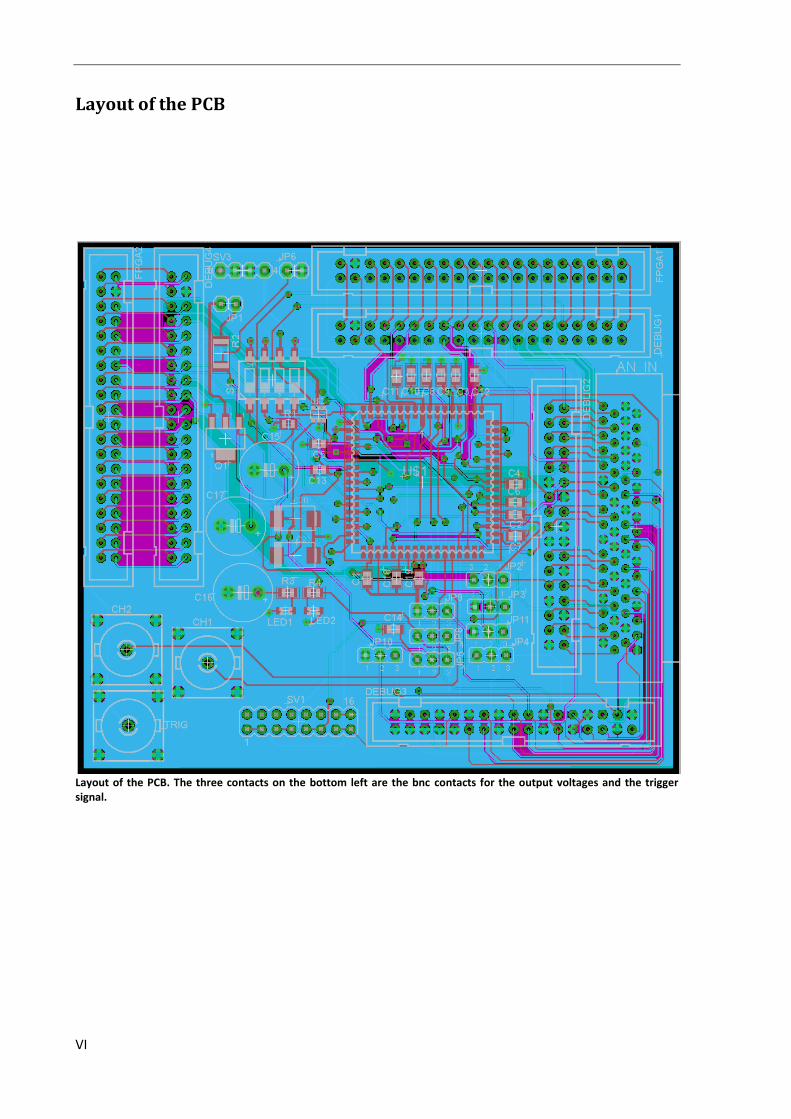
VI
Layout of the PCB
Layout of the PCB. The three contacts on the bottom left are the bnc contacts for the output voltages and the trigger signal.

VII
Appendix C - Timing diagrams
Appendix C Timing diagrams
The timing diagrams shown in this appendix are for illustration only. The y-axis is not valid, and all digital signals shown are 3.3 V logic.
Global reset
Timing diagram for global reset. The top two rows are the reset signals for the shift registers for Row Select (RS) and Column Select. The shift registers are reset to 0 both before and after the global reset.. The third row shows the D-signal into the first flip-flop in the Row Select circuit. It is kept high while the RS clock (fourth row) is ticked 32 times to enable all rows. When all rows are enabled, the reset_x goes high and resets all the pixels. For the sake of resetting the 4T pixels, Vtx_x also goes high. When 4T pixels are to be tested, the Vreset voltage is altered to adjust the pinning voltage of the buried photo diode. When all rows are reset, the shift registers are reset to 0 once more so that no rows are enabled.

VIII
3T readout
Timing diagram for readout of 3T pixels. The diagram shows the readout of one row plus storing of the values from the second row on the capacitor matrix. This diagram was made for illustration purposes to Morten Berg who made the programming file for the FPGA. Variation from these signals to the actual signals is small. The y-axis is not valid, all signals are low at 0 V and high at 3.3 V.
The top row shows the clock for the Row Select circuit. It goes high whenever a new row is to be selected. During one readout it goes high 32 times, two of which are shown here. The second row shows the reset signal, which goes directly into the pixels in the selected row. Next the sample_signal and sample_reset signals are shown. They control that the signal and reset values are stored on separate capacitors. The row select signal RS opens the row select transistor in the pixel so that the voltage value on the sensing node can be stored in the capacitor matrix. (RS is only one signal, but was simulated as two signals because of limitations in the spice program) The fifth row shows switching of the 4:1 multiplexers, who make sure that the capacitors are biased correctly during sampling. At this stage a bias voltage is presented at the output, which must be switched into all the capacitor matrix output lines. (The blue graphs are C0, and red C1.) The next row shows switching of the same signals during readout from the capacitor matrix. This time the bias voltage is switched off, so that the switches are operated as readout switches only. The seventh row illustrates the clock signal to the Column Select circuit. As shown, it goes high sixteen times during the readout of one row, reading out all 16 pixels in one channel. Thus, the stored values from four pixels are read out of the capacitor matrices at a time, two from each pixel matrix. The CS and CSC signals are equal, meaning that whenever a value is read out from the capacitor matrix, the switch between the two signal and reset storage capacitors is closed, so that the differential voltage is read out. The bottommost row shows how the different channels are read out. These signals are not presented to the circuit, but are used by the LabView system for sampling of the analog output values of the circuit.
0µs 8µs 16µs 24µs 32µs 40µs 48µs 56µs 64µs 72µs 80µs
0.0V
0.5V
1.0V
0.0V
0.5V
1.0V
0.0V
0.5V
1.0V
0.0V
0.5V
1.0V
0.0V
0.5V
1.0V
0.0V
0.5V
1.0V
0.0V
0.5V
1.0V
0.0V
0.5V
1.0V
0.0V
0.5V
1.0V
V(read_channel0) V(read_channel1) V(read_channel2) V(read_channel3)
V(csc) V(cs_x)
V(clk_cs)
V(c0) V(c1)
V(c0_sw_sig) V(c0_sw_rst) V(c1_sw_sig) V(c1_sw_rst)
V(rs_x1) V(rs_x2)
V(sample_s ignal) V(sample_reset)
V(reset_x)
V(clk_rs)

IX
Appendix D - Conference paper
Appendix D Conference paper
Abstract—The performances of optical pixels are
not well modeled in standard tools used by ASIC
designers. Hence, empirical knowledge based on a
library of implemented and measured pixels is
necessary. Such basis is especially important when
designing for high sensitivity for weak signals. An
optimal design should collect sufficient charge; have a
good charge to voltage conversion ratio and low noise
and leakage current. As a partner in a European
project SINTEF implemented a front end circuit
containing 520 x 40 pixels, amplifiers and ADCs. As
an additional add-on some test pixels where included
to get more empirical expertise on the performance of
different pixel architectures. This paper will report on
the test pixels only and ignore the main purpose and
application of the chip.
Index Terms—APS (Active Pixel Sensors), ASIC
(Application Specific Integrated Circuit), photo
sensors, silicon sensors
1. INTRODUCTION
Standard CMOS technologies are light sensitive
and by optimizing some parameters CMOS can
The development and production of the circuit that hosted the test structure was done through the I-ImaS [1,2] (Intelligent Imaging Sensors for Industry, Health and Security) project partly founded by the European Commission under the Sixth Framework Programme, Priority 3 NMP “New generation of sensors, actuators and systems for health, safety and security of people and environment”, contract no. NMP2-CT-2003-505593 and with additional support from the Norwegian Research Council. K.H. Løkken is a master student at the University of Oslo, Norway. J.M. Østby is senior research scientist with SINTEF ICT and an associate professor with the Department if Informatics, University of Oslo, Norway. (email: [email protected]).
compete with specialized technologies like CCD
[3,4]. A significant part of today’s digital cameras
have CMOS sensors. An advantage of the CMOS
technology is that both sensors and electronics can
be implemented on the same device.
The test structures described in this paper was
designed in the 0.35µm Opto CMOS process from
AMS. Available for the test pixels was a row of 512
pixels. Each pixel has a size of 32 x 32 µm. A test
unit consisting of 64 pixels was designed and
repeated 8 times along the 512 pixel long row.
Pixels and areas on both sides of the test row were
covered by metal. Thus we assume that the
influence from light on neighboring areas outside
the test row is ignorable.
The sensor consists of an n-well diffusion in a p-
substrate. The p-substrate is connected to the low
potential. Before exposure the n-well diffusion is
resat to a high potential. Incoming light generate
electron-hole pairs. The potential field between the
n-well and the substrate will attract the electrons to
the n-well. The accumulated charge in the n-well
will result in a reduced potential. The reduced
potential is measured and represents the amount of
light that has been received.
Each pixel consists of four elements: The n-well
diode that is the sensor element, a transistor that
resets that n-well potential to the high reference
value, a source follower transistor and a switch
transistor that connects to the common column bus.
Optical Test Pixels Implemented in a Standard
CMOS technology
K. H. Løkken, and J.M. Østby

X
Fig. 1. Top view and vertical cut of sensor diode in pixel. The
transistors are not drawn here.
Fig. 2. 3T pixel architecture
What we actually measure is the voltage on the
source follower gate. This voltage is related to the
charge according to: V=Q/C. The main
contributions to C are the capacitance of the n-well
diode and the gate capacitance of the source
follower transistor. One of the mayor trade-offs are
the size of the n-well diffusion. We would like to
have a large diffusion area to collect more of the
available charge. But on the other hand larger
diffusion area results in larger capacitance and
lower charge to voltage conversion ration. Larger
diffusion area will also result in more leakage
current and more shot noise. Another issue is the
size of the follower transistor. A larger source
follower transistor increases the transistor gain. But
a larger transistor does also have a larger gate
capacitance that reduces the voltage on the gate
representing the charge.
Since the difference between an optimal and a
non-optimal pixel design is significant, a reasonable
understanding of the physical parameters above is
required. Especially the charge collection and
capacitance as a function of diode size is important
but not well covered by standard ASIC design tools
and models. Hence empirically experience is
necessary.
2. THE TEST PIXELS
3. Reorganized pixel format to increase paper
readability
Fig. 3. Mapping between the actual 16x1 pixel row in the
layout and the 8x8 representation used in this paper.
To increase the readability the pixels of the 64 x 1
test unit are in the following drawn as an 8 x 8
matrix. Fig. 3 shows the reorganized drawing made
for this documentation.
4. The different types of test pixels
The first (topmost) line of fig. 4 contains the
same pixel architecture (defined as the standard or
reference pixel) but with different shielding. The
purpose is to get an impression of the sensitivity at
the different distances from the central sensor
diode.
Fig. 4. Test pixels drawn as an 8 x 8 matrix. Some of the pixels are pertly or fully covered by metal.
The second, fourth, sixth and eight lines are
equal except for the shielding of line four and eight.

XI
Appendix D - Conference paper
Pixel 13 and pixel 14 are variations with two and
four smaller diodes. Pixel 12, 14 and 15 all have the
same sensor diode size. The sensor size of pixel 11
is a little smaller than the others, sensor diode 10 is
two steps smaller while 9 and 10 are both three
steps smaller. The amplifier transistors in pixel 10,
11 and 12 are half of the standard while the
amplifier transistor in pixel 9 is one forth.
Line three and five are equal but line five are
covered by metal. In this line only the sensor diodes
have different size. Pixel 17 and 18 are three steps
smaller than the standard. Pixel 19 is two steps
smaller (same diode size as pixel 8 and 9). Pixel 20
is one step smaller than the standard. Pixels 21 and
22 have standard size while 23 and 24 are one step
larger.
Line seven contains only standard pixels but with
different shielding. The purpose of the pixels in this
line is to measure the influence of light on neighbor
pixels.
5. MEASUREMENT RESULTS
6. Reorganized pixel format to increase
readability
Since the test structure are repeated 8 times along
pixel row 39 we can chose between one or more of
these units. It seems that the highest channels
(which are closest to the bus drivers) are most
stable. Hence we chose to us the two 64 pixel units
at the higher end.
Fig. 5. Test pixels drawn as an 8 x 8 matrix. Some of the pixels are partly or fully covered by metal.
Fig. 6. Measured pixel gain given in % where 100% is the
average of the standard pixels within the test row while 0% is the
dark level.
We would like to compare performance of the
pixel variations with the performance of the
standard pixel. Hence we normalize the data so that
0% is the dark level and 100% is the average of the
14 standard pixels within the two test structures.
The results of the measurement on group 7 and 8
are shown in fig. 5. Each entry is the average of the
group 7 and group 8 values.
7. Neighbor influence
Before we discuss the measurements of the
individual pixels we have to look at the influence
by the neighbors. By studying fig. 6 we see that the
influence of light on neighbor pixels contribute
significantly to the measured values. We can see
this in several of the pixels. Since line 7 contains
only equal pixel cells with a variable shielding
pattern the size of this influence can be more easily
estimated here.
Pixel 52 is an unshielded pixel with one
uncovered pixel one each of two sides. This is
defined as the reference pixel between the test
pixels and the measured value is close to 100%. We
should note that all neighbors in the other directions
are shielded. Hence in the standard matrix where no
neighbors are covered the influence by neighbors is
larger and thus the measured value is larger (approx
120%).
The difference between pixel 51 and 53 relative
to pixel 52 is that one more of their neighbors are
covered by metal. This results in a reduction in the
measured value of about 10%.
Pixel 54 is it self covered by metal but one of the
neighbors are uncovered. The measured value is
12% of the reference value which corresponds well
with the previous observation.
Pixel 50 are covered it self but have two
Testpixel group 7 (ch 24-27) and 8 (ch 28-31) [1.38V]
0,4
0,6
0,8
1
1,2
1,4
1,6
1,8
0 16 32 48 64
Pixel number within group
Vo
ltag
e
Group 7
Group 8

XII
uncovered neighbors. The influence from these two
neighbors results in a measured value of 23%.
If we look in the areas with covered pixels the
measured values are close to 0% in the middle and
about 10% at the edges with uncovered neighbors.
We also see that uncovered pixels with a covered
neighbor have a reduction of about 10%.
From this we can conclude that each of the four
neighbor pixels contribute with about 10% of their
measured value to the inspected pixel.
8. Influence of diode size
Line 3 contains pixels with variable diode size.
We expect that a larger sensor diode collects more
charge. However a larger diode has larger
capacitance and hence reduces the charge to voltage
conversion ratio. Thus it is reasonable to assume
that at some size the increase in capacitance is
larger than the increase in collected charge resulting
in a reduced measured voltage.
Fig. 7. C, Q and V as function of diode size.
In fig 7 the measured voltage is given for the five
different diode sizes in line 3. The sensor
capacitance is estimated from the layout and given
in the figure. From these figures we calculate the
accumulated charge by multiplying the measured
voltage with the estimated capacitance. From the
figure we can see that both the collected charge and
the capacitance increase with the size of the sensor
diode. As expected at one point the increase in
capacitance is larger than the increase in collected
charge and the measured voltage starts to decrease.
In this particular case, given the other parameters as
source follower size etc. we can see that the optimal
size is somewhat smaller than the reference pixel
selected for the main pixel matrix.
9. Influence of transistor size
Line 2 and 6 contains pixels where not only the
sensor diode size is variable but also the transistor
size. In pixel 12 the sensor diode is standard but the
transistor size half. The transistor reduction results
in a 15% larger measured value.
Both pixel 10, 11 and 12 have half transistor
sizes. We find that reduction in sensor diodes
results in increased voltage signals. Pixel 9, 10 and
19 has a sensor size that is reduced two steps but
different transistor sizes. Pixel 19 with a standard
transistor size measure 118%, pixel 10 with a half
transistor size measure 128% while pixel 9 with a
quarter transistor size measure 140%. Since the
pixels are read by different amplifiers there may be
some errors but the tendency is believed to be
correct.
10. Behavior as function of light intensity
Fig. 8. Test pixel behavior for different light intensities
Fig.8 shows the measurements for some of the
test pixels and two standard pixels within the main
pixel matrix. The actual light intensity on chip is
believed to be proportional with the current through
the light source shown on the x-axis. Of the test
pixels on the figure we can see that pixel 9 has the
highest sensitivity and reaches the highest voltage
level. Pixel 13 is the opposite but also the pixel
which is linear over the largest part of light
intensity range and that saturate last. On the y-axis
it seems that the linear regions for the pixels are
between 0.6V and 1.4V for all of the pixels.
Fig. 8 shows also two standard pixels in the main
pixel matrix, one which is close to the dummy
shielding (Sch24r4c7) and one that is further away
from the shielding (Sch24r5c7). These pixels will
have a different performance since fewer of their
neighbors are covered by metal. None of the
neighbors of pixel Sch24r5c7 are covered by metal.
Hence this is the performance of most of the pixels
in the main pixel matrix.
11. CONCLUTION
Both from the influence from neighbors and from
Capacitance, collected charge and voltage for some
sensor sizes
60 %
70 %
80 %
90 %
100 %
110 %
120 %
-3 -2 -1 0 1
Sensor size
Perc
en
t re
lati
ve t
o r
efe
ren
ce p
ixel
C
Q
V
Some test pixels (group 7)
0,4
0,6
0,8
1
1,2
1,4
1,6
1,8
2
0 0,5 1 1,5 2 2,5 3 3,5
Current (relative consistence but uknown size)
Vo
ltag
e
T16std_7
T15std_7
T14_7
T13_7
T12_7
T11_7
T10_7
T9_7
T21std_7
T22std_7
T47std_7
T48std_7
T52std_7
Sch24r4c7
Sch24r5c7

XIII
Appendix D - Conference paper
the measurements on different diode sizes we see
that the diodes collect charge from a significantly
larger area than the diode area themselves. We also
find that there is an optimal pixel size that gives the
highest voltage.
ACKNOWLEDGMENT
The author would like to thank Roy Bahr and
Lars-Cyril Blystad for help with the design and
Morten Berg for very useful help with setting up
and developing the test equipment.
REFERENCES
[1] Web-cite for the I-ImaS project (Intelligent Image Sensors
for Industry, Health and Security): http://www.i-imas.ucl.ac.uk/
[2] R. Longo et al., ”Intelligent Imaging Sensors: System
development and preliminary results”, International Workshop on Digital Mammography (IWDM) 2006,
Manchester, UK, 18-21 June, 2006.
[3] E.R. Fossum, “CMOS image sensors: Electronic camera-on-a-chip,” IEEE Trans. Electron Devices, vol. 44, pp.
1689-1698, Oct. 1997.
[4] M. Sakakibra, “A High-Sensitivity CMOS Image Sensor With Gain-Adaptive Column Amplifiers”, IEEE Jour.
Solid State Circuits, vol. 40, no. 5, May 2005.

XIV
References
1. sentralbyrå, Statistisk. 2004. 2. Norwegian Radiation Protection Authority. Teknisk kvalitetskontroll i mammografiprogrammet. 2003. ISSN 0806-895X. 3. Cancer registry of Norway. Digital mammografiscreening. s.l. : Cancer registry of Norway, 2005. ISBN 82-90343-61-2. 4. Imaginis. Imaginis - History of Medical Diagnosis and Diagnostic Imaging. [Online] 13 September 2007. [Cited: 10 June 2008.] http://www.imaginis.com/faq/history.asp. 5. Siemens Medical. Computed Tomography - its History and Technology. [Online] [Cited: 10 June 2008.] http://www.medical.siemens.com/siemens/zh_CN/gg_ct_FBAs/files/brochures/CT_History_and_Technology.pdf. 6. James, J.J. The current status of digital mammography. Clinical Radiology. 2004. 7. Wililiamson, David. Digital mammography offers better breast cancer diagnoses. [Online] 1 December 1998. [Cited: 16 January 2008.] http://www.unc.edu/news/archives/dec98/pisano2.htm. 8. News-Medical.Net. Digital mammography no better than traditional film X-rays in the ability to detect breast cancer. [Online] 10 juni 2005. [Cited: 16 januar 2008.] http://www.news-medical.net/?id=10887. 9. Hauge IHR, Bredholt K, Pedersen K. Radiation doses to screened women in the NorwegianBreast Cancer Screening Program in 2005 and 2006. Østerås : Norwegian Radiation Protection Authority, 2007. ISSN 0804-4910. 10. Appleby, Alan, Ph.D, Costello, Martin, M.S. and Rose, Steven, M.S. 7. What Are the Health Effects of Ionizing Radiation? [Online] State University of New Jersey, Rutgers, 1996. [Cited: 16 januar 2008.] http://www.state.nj.us/dep/rpp/llrw/download/fact07.pdf. 11. Lazarou, John M. Digital mammography better at finding cancer in young women. [Online] 16 September 2005. [Cited: 16 January 2008.] http://www.hopkinsmedicine.org/Press_releases/2005/09_16_05.html. 12. Li, Flora M and Nathan, Arokia. CCD Image Sensors in Deep-Ultraviolet. s.l. : Springer, 2005. ISBN:354022680X. 13. Olsen, Alf. Lecture notes. Inf 5440 - CMOS image sensors. University of Oslo : s.n., 2007. 14. Østby, Joar Martin. Private conversation. September 2007. 15. Saint-Gobain Crystals. Sodium Iodide Datasheet. s.l. : Saint-Gobain Ceramics & Plastics, Inc, 2005. 16. Saint-Gobain crystals. Cesium Iodide, Scintillation Material - Data Sheet. s.l. : Saint-Gobain Ceramics & Plastics, Inc, 2007. 17. Shcerback, Igor and Yadid-Pect, Orly. Photoresponse Analysis and Pixel Shape Optimiation for CMOS Active Pixel Sensors. IEEE transactions on electron devices. 50, 2003. 18. Johns, David A and Martin, Ken. Analog integrated circuit design. s.l. : John Wiley & Sons, Inc, 1997. ISBN 0-471-14448-7. 19. Fossum, Erik R. CMOS active pixel image sensors. Nuclear Instruments & Methods in Physics Research. 1997.

XV
References
20. Motchenbacher, C. D. and Connelly, J. A. Low-Noise Electronic System Design. New York : John Wiley & Sons, Inc., 1993. ISBN 0-471-57742-1. 21. Nakamura, J. Image Sensors and Signal Processing for Digital Still Cameras. London : Taylor & Francis, 2006. ISBN 0-8493-3545-0. 22. Tian, Hui & al. Analysis of Temporal Noise in CMOS Photodiode Active Pixel Sensor. IEEE Journal of solid-state circuits. 2001. 23. Friedman, Edward and Miller, John Lester. Photonics Rules of Thumb. s.l. : McGraw-Hill Professional, 2003. ISBN:0071385193. 24. Cambridgeincolour.com. Tutorials - sharpness. [Online] Cambridge in colour. [Cited: 28 July 2008.] http://www.cambridgeincolour.com/tutorials/sharpness.htm. 25. Silvaco. Silvaco - products. [Online] Silvaco international, 1984. [Cited: 29 July 2008.] http://www.silvaco.com/products/products.html. 26. Fossum, Eric R, Dr. Visible Light CMOS Image Sensors. [Online] September 2003. [Cited: 13 June 2008.] http://www.slac.stanford.edu/econf/C020909/efslide.pdf. 27. Lee, Sungsik and Yang, Kyounghoon. A Novel Self-Adaptive Photosensing Active-Pixel Structure with Tunable Sensitivity for High Performance CMOS Image Sensors. IEEE SENSORS. 2006. 28. Lyon, Richard F. and Hubel, Paul M. Eyeing the Camera: into the Next Century. Santa Clara, California : Foveon, Inc.
