acon application note - powerstax · application note input voltage ... conserving battery power,...
TRANSCRIPT

ACONDC-DC CONVERTERS
TM
ACON, INC. • www.aconinc.com Rev. Dec. 21, 2004 Pg. 1 of 14
Application Note
Input Voltage The minimum and maximum input voltage which the
converter has been desinged to operate and within this voltage range the converter has been tested and met its specifications. Input voltage ranges of ACON DC-DC converters are as fol-lows.
Input voltage normally includes the ripple voltage as shown below. The ripple voltage shall be less than the following values.
When ripple voltage exceeds the above value, the out ripple voltage may become larger. The peak of input voltage wave shall be within the input voltage range.
Input Voltage Designator Input Voltage Range (Vdc)12 9 ~ 18 or 10 ~ 2024 18 ~ 36
24W 10 ~ 3630 10 ~ 3048 36 ~ 75
48W 20 ~ 72 or18 ~ 7560 20 ~ 60
Input Voltage Designator Input Ripple Voltage12 1.0 Vp-p24 2.0 Vp-p
24W 4.0 Vp-p30 4.0 Vp-p48 4.0 Vp-p
48W 4.0 Vp-p60 4.0 Vp-p
Time
Inpu
t Vol
tage
InputVoltageRange
RippleVoltage
Input FusingIn order to comply with safety requirements, the user must
provide a fuse in the input line. Fuses should also be used if the possibility of input polarity reversals exits. The fuse will cut off input power in the event of a catastrophic failure within the converter.
The fuse should have the current rating capable of withstanding the turn on inrush current but it should also be fast enough to blow to minimize the damage as much as possible.
It is recommended that the fuse be a slow-blow type with a current rating approximately 200% of the the full load input current to the converter.
Input Range (Vdc) 25W 50W 150W 200W 300W12 10 ~ 20 5A 8A 25A 30A 40A24 18 ~ 36 3A 4A 12A 15A 20A
24W 10 ~ 36 5A 8A 25A 30A 40A30 10 ~ 30 5A 8A 25A 30A 40A48 36 ~ 75 1.5A 3A 8A 10A 15A
48W 18 ~ 75 3A 4A 12A 15A 20A60 20 ~ 60 3A 4A 12A 15A 20A
Exclusively distributed by Powerstax
ACONDC-DC CONVERTERS
TM
ACON, INC. • www.aconinc.com Rev. Dec. 21, 2004 Pg. 2 of 14
Application Note
Sample Plot, 24Vin - 3.3Vout4.0
Out
put (
V)
3.0
2.0
1.0
0.014.0 15.0 16.0 17.0 18.0 19.0 20.0
Input Voltage (V)
Under-Voltage Lockout
Reverse Voltage ProtectionInput reverse polarity can be protected with a series diode
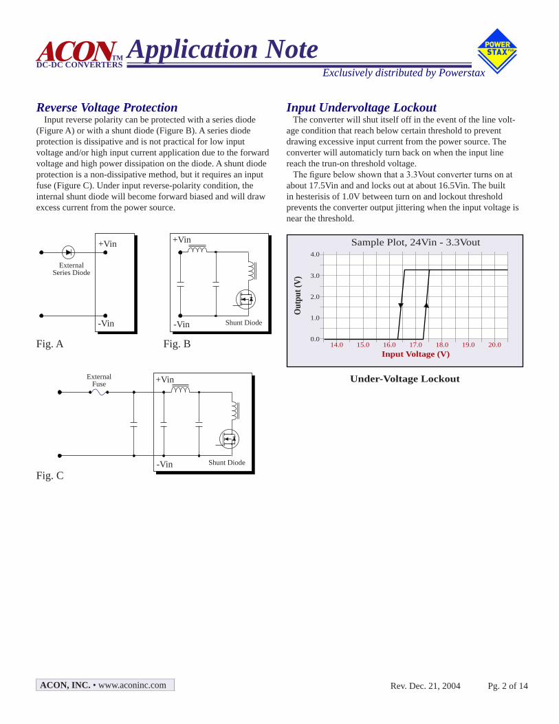
(Figure A) or with a shunt diode (Figure B). A series diode protection is dissipative and is not practical for low input voltage and/or high input current application due to the forward voltage and high power dissipation on the diode. A shunt diode protection is a non-dissipative method, but it requires an input fuse (Figure C). Under input reverse-polarity condition, the internal shunt diode will become forward biased and will draw excess current from the power source.
+Vin
-Vin Shunt Diode
ExternalSeries Diode
+Vin
-Vin
Fig. A Fig. B
+Vin
-Vin Shunt Diode
ExternalFuse
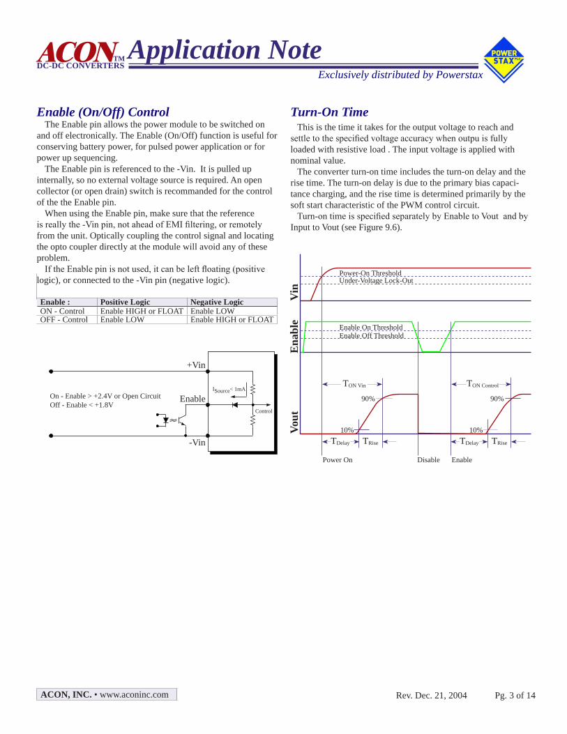
Input Undervoltage Lockout The converter will shut itself off in the event of the line volt-age condition that reach below certain threshold to prevent drawing excessive input current from the power source. The converter will automaticly turn back on when the input line reach the trun-on threshold voltage. The figure below shown that a 3.3Vout converter turns on at about 17.5Vin and and locks out at about 16.5Vin. The built in hesterisis of 1.0V between turn on and lockout threshold prevents the converter output jittering when the input voltage is near the threshold.
Fig. C
Exclusively distributed by Powerstax
ACONDC-DC CONVERTERS
TM
ACON, INC. • www.aconinc.com Rev. Dec. 21, 2004 Pg. 3 of 14
Application Note
Enable (On/Off) ControlThe Enable pin allows the power module to be switched on
and off electronically. The Enable (On/Off) function is useful for conserving battery power, for pulsed power application or for power up sequencing.
The Enable pin is referenced to the -Vin. It is pulled up internally, so no external voltage source is required. An open collector (or open drain) switch is recommanded for the control of the the Enable pin.
When using the Enable pin, make sure that the reference is really the -Vin pin, not ahead of EMI filtering, or remotely from the unit. Optically coupling the control signal and locating the opto coupler directly at the module will avoid any of these problem.
If the Enable pin is not used, it can be left floating (positive logic), or connected to the -Vin pin (negative logic).
Enable : Positive Logic Negative LogicON - Control Enable HIGH or FLOAT Enable LOWOFF - Control Enable LOW Enable HIGH or FLOAT
+Vin
-Vin
Control
ISource< 1mA
EnableOn - Enable > +2.4V or Open CircuitOff - Enable < +1.8V
Turn-On Time This is the time it takes for the output voltage to reach and settle to the specified voltage accuracy when outpu is fully loaded with resistive load . The input voltage is applied with nominal value. The converter turn-on time includes the turn-on delay and the rise time. The turn-on delay is due to the primary bias capaci-tance charging, and the rise time is determined primarily by the soft start characteristic of the PWM control circuit. Turn-on time is specified separately by Enable to Vout and by Input to Vout (see Figure 9.6).
TDelay TRise
10%
90%
Power-On ThresholdUnder-Voltage Lock-Out
Vin
TDelay TRise
10%
90%
Enable On ThresholdEnable Off Threshold
TON Vin TON Control
Ena
ble
Vout
Power On Disable Enable
Exclusively distributed by Powerstax
ACONDC-DC CONVERTERS
TM
ACON, INC. • www.aconinc.com Rev. Dec. 21, 2004 Pg. 4 of 14
Application NoteInput Filtering DC-DC converters by nature generate significant levels of both conducted and radiated noise. There are two types of con-ducted noise: common mode and differential mode noise. The common mode noise is directly related to the effective parasitic capacitance between the power module input conductors and chassis ground. The differential mode noise is across the input conductors. It is recommended to have some level of EMI sup-pression to the power module.
Conducted noise on the input power lines can occur as either differential or common-mode noise currents. The required standard for conducted emissions is EN55022 Class A (FCC Part 15).
+Vout
-Vout
LOA
D+Vin
-Vin
Conducted EMI
CommonMode
CommonMode
DifferentialMode
+Vout
-Vout
LOA
D
+Vin
-Vin
External Common Mode Filter
+Vout
-Vout
LOA
D
+Vin
-Vin
Basic Connection
+ ++
+S
-SEnable
Fuse
C1 C2 C3
L1
Input Refelcted Ripple CurrentConverter is drawing current from input power source only
when the input switch is on. This creates a pulsation current flow from the input source. The reflected ripple current is measured as a peak-to-peak current with a current probe over 0 to 20MHz bandwidth. Ripple current can be suppressed by an external Π (pi) filter as shown below.
Input Reflected Ripple Current
+Vin
-Vin
C1C2
L1 = 12µH
ICIS
C1 = 47µF, ESR < 1Ω @ 100KHzC2 = 220µF, ESR < 100mΩ @ 100KHzIC = Reflected Ripple Current without External LC FilterIS = Reflected Ripple Current with External LC Filter
Vin+_
Exclusively distributed by Powerstax
ACONDC-DC CONVERTERS
TM
ACON, INC. • www.aconinc.com Rev. Dec. 21, 2004 Pg. 5 of 14
Application Note
Line RegulationThe percent change in output voltage when the input voltage
is swing from rated minimu (Low Line) to rated maximum (High Line) while the out is fully loaded.
Load RegulationThe percent change in output voltage when the output load is
switched from minimum rated load to maximum rated load.
Cross RegulationIn a multiple output power supply, the percent voltage change at one output caused by the load change on another output. See Figure below.
Transient ResponseThe time it takes for the output voltage to settle to the
specified voltage accuracy after the 25% output load change.
Screen Shot of Load Transient
Overshoot
Load Transient
Undershoot
PeakDeviation
Voltage Accuracy
Tranisent Response Time
25% Load Transient
Cross Regulation(±15Vout vs +5Vload)
17.0
±15V
Out
put (
V) 16.0
15.0
14.0
13.0100 200 300 400 500
±15V Loading (mA)
5V @ 4.0A
5V @ 0.5A
Exclusively distributed by Powerstax

ACONDC-DC CONVERTERS
TM
ACON, INC. • www.aconinc.com Rev. Dec. 21, 2004 Pg. 6 of 14
Application Note
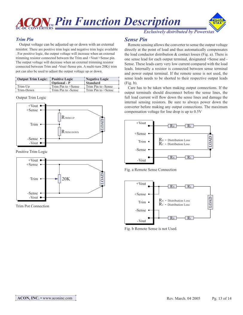
Remote SensingRemote sensing allows the converter to sense the output voltage
directly at the point of load and thus automatically compensates the load conductor distribution & contact losses (Fig. a). There is one sense lead for each output terminal, designated +Sense and -Sense. These leads carry very low current compared with the load leads. Internally a resistor is connected between sense terminal and power output terminal. If the remote sense is not used, the sense leads needs to be shorted to their respective output leads (Fig. b).
Care has to be taken when making output connections. If the output terminals should disconnect before the sense lines, the full load current will flow down the sense lines and damage the internal sensing resistors. Be sure to always power down the converter before making any output connections. The maximum compensation voltage for line drop is up to 0.5V
+Vout
-Vout
LOA
D
+Sense
-Sense
Trim
Fig. b Remote Sense is not Used.
RD RC
RD RC
RD - Distribution LossRC - Distribution Loss
+Vout
-Vout
LOA
D
+Sense
-Sense
Trim
Fig. a Remote Sense Connection
RD RC
RD RC
RD - Distribution LossRC - Distribution Loss
Output Ripple & NoiseThe output ripple is composed of fundamental frequency
ripple and high frequency switching noise spikes. The fundamental switching frequency ripple (or basic ripple) is in the 100KHz to 1MHz range; the high frequency switching noise spike (or switching noise) is in the 10 MHz to 50MHz range. The switching noise is normally specified with 20 MHz bandwith to include all significant harmonics for the noise spikes. In the case of switching power supplies and DC-DC convert-ers, the output ripple is composed of fundamental frequency ripple and high frequency switching noise spikes. The funda-mental switching frequency ripple (or basic ripple) is in the 100KHz to 1MHz range; the high frequency switching noise spike (or switching noise) is in the 10 MHz to 50MHz range. The switching noise is normally specified with 20 MHz band-with to include all significant harmonics for the noise spikes.
The easiest way to measure the output ripple and noise is to use an oscilloscope probe tip and ground ring pressed directly aganist the power converter ouptut pins, as shown below. This makes the shortest possible connection across the output terminals.
The oscilloscope probe groud clip should never be used in the ripple and noise measurement. The ground clip will not only act as an antena and pick-up the the radiated high frequency energy, it will introduce the common-mode noise to the measurement as well.
The standard test setup for ripple & noise measurements is shown in Figure 9.9a. A probe socket (Tektronix, P.N. 131.0258-00) is used for the measurements to eliminate noise pickup associated with long ground clip of scope probes.
Exclusively distributed by Powerstax

ACONDC-DC CONVERTERS
TM
ACON, INC. • www.aconinc.com Rev. Dec. 21, 2004 Pg. 7 of 14
Application Note
Output Ripple & Noise
NoiseRipple
+Vout
-Vout
0.1uF
Probe Socket
Copper Strips (2-3”)
Output Ripple & Noise Measurement
LOA
D
Scope Ground RingScope Tip
Unit Under Test
Simplified Ripple & Noise Measurement
X1 Probe
Output Voltage TrimOutput voltage can be adjusted up or down with an external
resistor. There are positive trim logic and negative trim logic available . For positive logic, the output voltage will increase when an external trimming resistor connected between the Trim and +Vout/+Sense pin. The output voltage will decrease when an external trimming resistor connected between Trim and -Vout/-Sense pin. A multi-turn 20Ký trim pot can also be used to adjust the output voltage up or down.
+Vout
-Vout
LOA
D
+Sense
-Sense
Trim
RTRIM-UP
RTRIM-DOWN
Positive Trim Logic
Output Trim Logic: Positive Logic Negative LogicOptional - P Standard
Trim-Up Trim Pin to +Sense Trim Pin to -SenseTrim-Down Trim Pin to -Sense Trim Pin to +Sense
Output Trim Logic
+Vout
-Vout
LOA
D
+Sense
-Sense
Trim 20K
Trim Pot Connection
Exclusively distributed by Powerstax

ACONDC-DC CONVERTERS
TM
ACON, INC. • www.aconinc.com Rev. Dec. 21, 2004 Pg. 8 of 14
Application Note
Output LoadingThere is a minimum load required for most of converter
output. Specially for those multiple output converters that use only one PWM (Pulse Width Modulator) controller. Load regulation is usually tested from minimum rated load to maximum rated load.
Output Overvoltage ProtectionTo Preventing damage to the user’s circuitry in the event of
broken feedback control loop, the main output is limited by an internal clamp typically @ 120% of rated output. An accurate overvoltage clamp can be implemented externally vai the Enable pin.
Hiccup Mode Short Circuit ProtectionUnder output faulty condition (short circuit), the converter
goes into hiccup short circuit protection mode and limits the output current both in peak value and duration time. Once the faulty condition removed, the converter automatically exits the hiccup mode and continues normal operation.
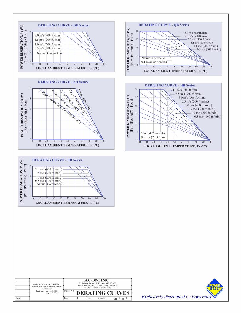
0 10 20 30 40 50 60 70 80 90 100
4
2
0
LOCAL AMBIENT TEMPERATURE, TA (°C)
DERATING CURVE6
Natural Convection.0.5 m/s (100 ft./min.)1.0 m/s (200 ft./min.)1.5 m/s (300 ft./min.)2.0 m/s (400 ft./min.)
POW
ER
DIS
SIPA
TIO
N, P
D (W
)P
D =
(PO
UT
/eff
.) - P
OU
T
Typical Derating Curve
POUT , Output Power (Watt)η = POUT /PIN , Efficiency PIN = POUT / η , Input Power (Watt) θ , Thermal Impedance (°C/Watt)PDISS = PIN - POUT , Power DissipationTRISE = PDISS x θ , Temperature Rise (°C)
PIN POUTPDISS
TRISE = PDISS x θ
θ
Temperature Rise
Thermal ImpedanceThe temperature rise of the converter is the product of power
dissipation and thermal impedance, TRISE = PDISS x θ. The figure below illustrates the relationships of output power and temperature rise.
+Vin
-Vin
Control
ISource< 1mA
EnableOn - Enable > +2.4V or Open CircuitOff - Enable < +1.8V
Exclusively distributed by Powerstax

ACONDC-DC CONVERTERS
TM
ACON, INC. • www.aconinc.com Rev. Dec. 21, 2004 Pg. 9 of 14
Application Note
High Capacitive Load
+S
-S
+48V
-48V
Trim
1N4448
100K
499K
10V
0.022µF
2N2907 IRF540N
25Ω/2W
+10,000µF
FH50
S244
818
-36V
in48
Vout
@1.
04A
Capacitive LoadingOutput capacitors draw charging current during the startup
phase of DC-DC converters. This capacitive charging current become very significant specifically for high output voltage with high capacitive loading. The initial surge input current could exceed the current limit threshold and trigger the short circuit protection circuitry and send the converter running into the hiccup mode. Converters in hiccup mode show an abnormally low output voltage.
The circuit shown below can charge the 10000µF capacitor to 48V without triggering the converter protection circuitry.
EnableThis pin provides the remote On/Off control function. Two control logics are available: Positive & Negative. Positive logic turns the module ON during a logic high voltage on the enable pin, and OFF during a logic low. Negative logic turns the mod-ule OFF during a logic high and ON during a logic low. Positive logic is the standard factor configuration. Negative Enable Logic can be specified with suffix N. The Enable pin can be left float-ing if not used.
Sync-InThis pin can be connected either to external clock or directly to the Sync-In pin of another MKS, MKD or MKT module. If the Sync-In pin is connected to another module's Sync-In pin, the connection should be as direct as possible, and the Vin(-) pins of the modules must be shorted together. If an external clock signal is applied to the Sync-In pin, the signal must be a 300KHz (±30KHz) square wave with a ≥ 4 Vp-p amplitude. The Sync-In pin can be left floating if not used.
I-ShareTwo or more modules can be operated in parallel for either redundant operation or additional power requirements. Connect I-Share pin together will force load sharing between the con-nected modules. To implement forced load sharing, the Sync-In pins of all units must be connected together also. The I-Share pin can be left floating if not used.
Sync-OutThis pin contains a clock signal referenced to the (-)Vout pin. The frequency of this signal will equal either the module's inter-nal clock frequency or the frequency established by an external clock applied to the Sync-In pin. The Sync-Out pin can be left floating if not used.
PG (PWR GOOD)The PWR GOOD pin indicates the operating state of the module. A TTL high indicates that the Vout is within ±15% of voltage set-point. A TTL low indicates that the Vout is out of regulation. The PG pin can be left floating if not used.
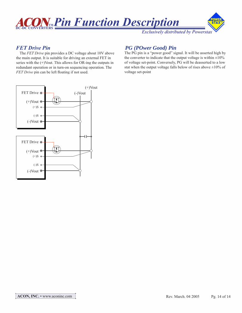
FET DriveThe FET Drive pin provides a DC voltage about 10V above the main output. It is suitable for driving an external FET in series with the (+)Vout. This allows for OR-ing the outputs in redun-dant operation or in turn-on sequencing operation. The FET Drive pin can be left floating if not used.
Exclusively distributed by Powerstax
Unless Otherwise Specifi edDimension are in Inches (mm)
Tolerances:Decimals .xx ± 0.020 .xxx ± 0.005
ACON, INC.22 Bristol Drive, S. Easton, MA 02375
Tel : (508)230-8022 ; Fax (508) 230-2371E-Mail : www.aconinc.com
Model No. DERATING CURVESDate Rev: 1 Date: 11/4/02 SH 1 of 1 of 1 of
0 10 20 30 40 50 60 70 80 90 100
30
15
10
5
0
LOCAL AMBIENT TEMPERATURE, TA (°C)
POW
ER
DIS
SIPA
TIO
N, P
D (W
)P
D =
(PO
UT
/eff
.) - P
OU
T
DERATING CURVE - HB Series
20
25
4.0 m/s (800 ft./min.) 3.5 m/s (700 ft./min.) 3.0 m/s (600 ft./min.) 3.0 m/s (600 ft./min.) 2.5 m/s (500 ft./min.) 2.5 m/s (500 ft./min.) 2.5 m/s (500 ft./min.) 2.5 m/s (500 ft./min.) 2.5 m/s (500 ft./min.) 2.5 m/s (500 ft./min.) 2.0 m/s (400 ft./min.) 2.0 m/s (400 ft./min.) 2.0 m/s (400 ft./min.) 2.0 m/s (400 ft./min.) 2.0 m/s (400 ft./min.) 2.0 m/s (400 ft./min.) 2.0 m/s (400 ft./min.) 2.0 m/s (400 ft./min.) 2.0 m/s (400 ft./min.) 2.0 m/s (400 ft./min.) 2.0 m/s (400 ft./min.) 1.5 m/s (300 ft./min.) 1.5 m/s (300 ft./min.) 1.5 m/s (300 ft./min.) 1.5 m/s (300 ft./min.) 1.5 m/s (300 ft./min.) 1.5 m/s (300 ft./min.) 1.5 m/s (300 ft./min.) 1.5 m/s (300 ft./min.) 1.5 m/s (300 ft./min.) 1.0 m/s (200 ft./min.) 1.0 m/s (200 ft./min.) 1.0 m/s (200 ft./min.) 1.0 m/s (200 ft./min.) 1.0 m/s (200 ft./min.) 1.0 m/s (200 ft./min.) 1.0 m/s (200 ft./min.) 1.0 m/s (200 ft./min.) 1.0 m/s (200 ft./min.) 1.0 m/s (200 ft./min.) 1.0 m/s (200 ft./min.) 0.5 m/s (100 ft./min.) 0.5 m/s (100 ft./min.) 0.5 m/s (100 ft./min.) 0.5 m/s (100 ft./min.) 0.5 m/s (100 ft./min.) 0.5 m/s (100 ft./min.) 0.5 m/s (100 ft./min.) 0.5 m/s (100 ft./min.) 0.5 m/s (100 ft./min.) 0.5 m/s (100 ft./min.) 0.5 m/s (100 ft./min.)
Natural Con vec tionNatural Con vec tionNatural Con vec tionNatural Con vec tionNatural Con vec tion0.1 m/s (20 ft./min.)
0 10 20 30 40 50 60 70 80 90 100
4
2
0
LOCAL AMBIENT TEM PER A TURE, TA (°C)
DERATING CURVE - DH Series
6
Natural ConvectionNatural ConvectionNatural ConvectionNatural ConvectionNatural ConvectionNatural ConvectionNatural ConvectionNatural ConvectionNatural ConvectionNatural ConvectionNatural ConvectionNatural Convection0.5 m/s (100 ft./min.)0.5 m/s (100 ft./min.)0.5 m/s (100 ft./min.)0.5 m/s (100 ft./min.)0.5 m/s (100 ft./min.)1.0 m/s (200 ft./min.)1.0 m/s (200 ft./min.)1.0 m/s (200 ft./min.)1.0 m/s (200 ft./min.)1.0 m/s (200 ft./min.)1.5 m/s (300 ft./min.)1.5 m/s (300 ft./min.)1.5 m/s (300 ft./min.)1.5 m/s (300 ft./min.)1.5 m/s (300 ft./min.)2.0 m/s (400 ft./min.)2.0 m/s (400 ft./min.)2.0 m/s (400 ft./min.)2.0 m/s (400 ft./min.)2.0 m/s (400 ft./min.)
POW
ER
DIS
SIPA
TIO
N, P
D (W
)P
D =
(PO
UT
/eff
.) - P
OU
T
0 10 20 30 40 50 60 70 80 90 100
10
4
2
0
LOCAL AMBIENT TEM PER A TURE, TA (°C)
DERATING CURVE - EH Series
6
8
Natural Convection, 0.1 m/s (20 ft./min.)
Natural Convection, 0.1 m/s (20 ft./min.)
Natural Convection, 0.1 m/s (20 ft./min.)
Natural Convection, 0.1 m/s (20 ft./min.)
Natural Convection, 0.1 m/s (20 ft./min.)
Natural Convection, 0.1 m/s (20 ft./min.)
Natural Convection, 0.1 m/s (20 ft./min.)
Natural Convection, 0.1 m/s (20 ft./min.)
Natural Convection, 0.1 m/s (20 ft./min.)
Natural Convection, 0.1 m/s (20 ft./min.)
Natural Convection, 0.1 m/s (20 ft./min.)
0.5 m/s (100 ft./min.)
0.5 m/s (100 ft./min.)
0.5 m/s (100 ft./min.)
0.5 m/s (100 ft./min.)
0.5 m/s (100 ft./min.)
0.5 m/s (100 ft./min.)
0.5 m/s (100 ft./min.)
1.0 m/s (200 ft./min.)
1.0 m/s (200 ft./min.)
1.0 m/s (200 ft./min.)
1.0 m/s (200 ft./min.)
1.0 m/s (200 ft./min.)
1.0 m/s (200 ft./min.)
1.0 m/s (200 ft./min.)
1.5 m/s (300 ft./min.)
1.5 m/s (300 ft./min.)
1.5 m/s (300 ft./min.)
1.5 m/s (300 ft./min.)
1.5 m/s (300 ft./min.)
1.5 m/s (300 ft./min.)
2.0 m/s (400 ft./m
in.)
POW
ER
DIS
SIPA
TIO
N, P
D (W
)P
D =
(PO
UT
/eff
.) - P
OU
T
0 10 20 30 40 50 60 70 80 90 100
4
2
0
LOCAL AMBIENT TEM PER A TURE, TA (°C)
DERATING CURVE - FH Series6
Natural Convection.Natural Convection.Natural Convection.Natural Convection.Natural Convection.0.5 m/s (100 ft./min.)0.5 m/s (100 ft./min.)0.5 m/s (100 ft./min.)0.5 m/s (100 ft./min.)0.5 m/s (100 ft./min.)1.0 m/s (200 ft./min.)1.0 m/s (200 ft./min.)1.0 m/s (200 ft./min.)1.0 m/s (200 ft./min.)1.0 m/s (200 ft./min.)1.5 m/s (300 ft./min.)1.5 m/s (300 ft./min.)1.5 m/s (300 ft./min.)1.5 m/s (300 ft./min.)1.5 m/s (300 ft./min.)2.0 m/s (400 ft./min.)2.0 m/s (400 ft./min.)2.0 m/s (400 ft./min.)2.0 m/s (400 ft./min.)2.0 m/s (400 ft./min.)
POW
ER
DIS
SIPA
TIO
N, P
D (W
)P
D =
(PO
UT
/eff
.) - P
OU
T
0 10 20 30 40 50 60 70 80 90 100
15
10
5
0
LOCAL AMBIENT TEMPERATURE, TA (°C)POW
ER
DIS
SIPA
TIO
N, P
D (W
)P
D =
(PO
UT
/eff
.) - P
OU
T
DERATING CURVE - QB Series20
3.0 m/s (600 ft./min.) 2.5 m/s (500 ft./min.) 2.5 m/s (500 ft./min.) 2.5 m/s (500 ft./min.) 2.0 m/s (400 ft./min.) 2.0 m/s (400 ft./min.) 2.0 m/s (400 ft./min.) 2.0 m/s (400 ft./min.) 1.5 m/s (300 ft./min.) 1.5 m/s (300 ft./min.) 1.5 m/s (300 ft./min.) 1.5 m/s (300 ft./min.) 1.5 m/s (300 ft./min.) 1.5 m/s (300 ft./min.) 1.0 m/s (200 ft./min.) 1.0 m/s (200 ft./min.) 1.0 m/s (200 ft./min.) 1.0 m/s (200 ft./min.) 1.0 m/s (200 ft./min.) 1.0 m/s (200 ft./min.) 0.5 m/s (100 ft./min.) 0.5 m/s (100 ft./min.) 0.5 m/s (100 ft./min.) 0.5 m/s (100 ft./min.) 0.5 m/s (100 ft./min.) 0.5 m/s (100 ft./min.) 0.5 m/s (100 ft./min.) 0.5 m/s (100 ft./min.) 0.5 m/s (100 ft./min.)
Natural Con vec tionNatural Con vec tionNatural Con vec tionNatural Con vec tionNatural Con vec tion0.1 m/s (20 ft./min.)
Exclusively distributed by Powerstax

ACONDC-DC CONVERTERS
TM
ACON, INC. • www.aconinc.com Rev. March. 04 2005 Pg. 11 of 14
Pin Function Description
Enable : Positive LogicPositive Logic Negative LogicNegative LogicON - Control Enable HIGH or FLOAT Enable LOWOFF - Control Enable LOW Enable HIGH or FLOAT
+Vin
-Vin
Control
ISource< 1mA
EnableOn - Enable > +2.4V or Open CircuitOff - Enable < +1.8V
Enable (On/Off Control) PinThe Enable pin allows the power module to be switched on
and off electronically. The Enable (On/Off) function is useful for conserving battery power, for pulsed power application or for power up sequencing.
The Enable pin is referenced to the -Vin. It is pulled up internally, so no external voltage source is required. An open collector (or open drain) switch is recommanded for the control of the the Enable pin.
When using the Enable pin, make sure that the reference is really the -Vin pin, not ahead of EMI fi ltering, or remotely from the unit. Optically coupling the control signal and locating the opto coupler directly at the module will avoid any of these problem.
Two control logics are available: Positive & Negative. Posi-tive logic turns the module ON during a logic high voltage on the enable pin, and OFF during a logic low. Negative logic turns the module OFF during a logic high and ON during a logic low. Positive logic is the standard factor confi guration. Negative Enable Logic can be specifi ed with suffi x N.
If the Enable pin is not used, it can be left fl oating (positive logic), or connected to the -Vin pin (negative logic).
Sync-InThis pin can be connected either to external clock or directly
to the Sync-In pin of another MKS, MKD or MKT module. If the Sync-In pin is connected to another module's Sync-In pin, the connection should be as direct as possible, and the Vin(-) pins of the modules must be shorted together. If an external clock signal is applied to the Sync-In pin, the signal must be a 300KHz (±30KHz) square wave with a ≥ 4 Vp-p amplitude. The Sync-In pin can be left fl oating if not used.
Sync- In
I-Share(+)Vin
(-)Vin(-)Vin
External Clock (Optional)(270KHz ~ 340KHz)
100ρF
1KΩ
(+)Vin
(-)Vin
Sync- In
I-Share
(+)Vin
(-)Vin
Exclusively distributed by Powerstax

ACONDC-DC CONVERTERS
TM
ACON, INC. • www.aconinc.com Rev. March. 04 2005 Pg. 12 of 14
Pin Function Description
Two or more modules can be operated in parallel for either redundant operation or additional power requirements. Connect I-Share pin together will force load sharing between the con-nected modules. To implement forced load sharing, the Sync-In pins of all units must be connected together also. The I-Share pin can be left fl oating if not used.
Sync- In
I-Share(+)Vin
(-)Vin(-)Vin(+)Vin
(-)Vin
Sync- In
I-Share
(+)Vin
(-)Vin
I-Share Sync-OutThis pin contains a clock signal referenced to the (-)Vout pin.
The frequency of this signal will equal either the module's inter-nal clock frequency or the frequency established by an external clock applied to the Sync-In pin. The Sync-Out pin can be left fl oating if not used.
Exclusively distributed by Powerstax
ACONDC-DC CONVERTERS
TM
ACON, INC. • www.aconinc.com Rev. March. 04 2005 Pg. 13 of 14
Pin Function DescriptionTrim Pin
Output voltage can be adjusted up or down with an external resistor. There are positive trim logic and negative trim logic available . For positive logic, the output voltage will increase when an external trimming resistor connected between the Trim and +Vout/+Sense pin. The output voltage will decrease when an external trimming resistor connected between Trim and -Vout/-Sense pin. A multi-turn 20Ký trim pot can also be used to adjust the output voltage up or down.
+Vout
-Vout
LOA
D
+Sense
-Sense
Trim
RTRIM-UP
RTRIM-DOWN
Positive Trim Logic
Output Trim Logic: Positive Logic Negative LogicOptional - POptional - P Standard
Trim-UpTrim-Up Trim Pin to +Sense Trim Pin to -SenseTrim-Down Trim Pin to -Sense Trim Pin to +Sense
Output Trim Logic
+Vout
-Vout
LOA
D
+Sense
-Sense
Trim 20K
Trim Pot Connection
Sense PinRemote sensing allows the converter to sense the output voltage
directly at the point of load and thus automatically compensates the load conductor distribution & contact losses (Fig. a). There is one sense lead for each output terminal, designated +Sense and -Sense. These leads carry very low current compared with the load leads. Internally a resistor is connected between sense terminal and power output terminal. If the remote sense is not used, the sense leads needs to be shorted to their respective output leads (Fig. b).
Care has to be taken when making output connections. If the output terminals should disconnect before the sense lines, the full load current will fl ow down the sense lines and damage the internal sensing resistors. Be sure to always power down the converter before making any output connections. The maximum compensation voltage for line drop is up to 0.5V
+Vout
-Vout
LOA
D
+Sense
-Sense
Trim
Fig. b Remote Sense is not Used.
RD RC
RD RC
RDRDR - Distribution LossRC - Distribution Loss
+Vout
-Vout
LOA
D
+Sense
-Sense
Trim
Fig. a Remote Sense Connection
RD RC
RD RC
RDRDR - Distribution LossRC - Distribution Loss
Exclusively distributed by Powerstax
ACONDC-DC CONVERTERS
TM
ACON, INC. • www.aconinc.com Rev. March. 04 2005 Pg. 14 of 14
Pin Function Description
The PG pin is a “power good” signal. It will be asserted high by the converter to indicate that the output voltage is within ±10% of voltage set-point. Conversely, PG will be deasserted to a low stat when the output voltage falls below of rises above ±10% of voltage set-point
FET Drive Pin PG (POwer Good) PinThe FET Drive pin provides a DC voltage about 10V above
the main output. It is suitable for driving an external FET in series with the (+)Vout. This allows for OR-ing the outputs in redundant operation or in turn-on sequencing operation. The FET Drive pin can be left fl oating if not used.
FET Drive
(+)Vout(+)S
(-)S
FET Drive
(+)S
(-)S
(-)Vout
(+)Vout
(-)Vout
(+)Vout(-)Vout
Exclusively distributed by Powerstax