accurate modeling of the delay and energy overhead of
TRANSCRIPT

1
Accurate Modeling of the Delay and EnergyOverhead of Dynamic Voltage and Frequency
Scaling in Modern MicroprocessorsSangyoung Park Student Member, IEEE, Jaehyun Park Student Member, IEEE, Donghwa Shin Student
Member, IEEE, Yanzhi Wang Student Member, IEEE, Qing Xie Student Member, IEEE, NaehyuckChang Fellow, IEEE, and Massoud Pedram Fellow, IEEE
Abstract—Dynamic voltage and frequency scaling (DVFS) hasbeen studied for well over a decade. The state-of-the-art DVFStechnologies and architectures are advanced enough such thatthey are employed in most commercial systems today. Never-theless, existing DVFS transition overhead models suffer fromsignificant inaccuracies, for example, by correctly accountingfor the effect of DC-DC converters, frequency synthesizers,and voltage and frequency change policies on energy lossesincurred during mode transitions. Incorrect and/or inaccurateDVFS transition overhead models prevent one from determiningthe precise break-even time and thus forfeit some of the energysaving that is ideally achievable. Through detailed analysis ofmodern DVFS setups and voltage and frequency change policiesprovided by commercial vendors, this paper introduces accurateDVFS transition overhead models for both energy consumptionand delay. In particular, we identify new contributors to theDVFS transition overhead including the underclocking-relatedlosses in a DVFS-enabled microprocessor, additional inductorIR losses, and power losses due to discontinuous-mode DC-DC conversion. We report the transition overheads for threerepresentative processors: Intel Core2Duo E6850, ARM Cortex-A8, and TI MSP430. Finally, we present a compact, yet accurate,DVFS transition overhead macro model for use by high-levelDVFS schedulers.
I. INTRODUCTION
DYNAMIC voltage and frequency scaling (DVFS) hasproved itself as one of the most successful energy saving
techniques for a wide range of processors from ultra low-power microprocessors for embedded applications such as theTI MSP430 to high-performance microprocessors for desktopsand servers such as the Intel’s SpeedStep Technology [1]and the AMD equivalent PowerNow!. DVFS is enabled byprogrammable DC–DC converter and a programmable clockgenerator. These devices naturally incur overhead wheneverthe system changes its voltage and frequency setting. Sincethe DVFS break-even time is strongly dependent on the DVFStransition overhead [2], correct overhead estimation is crucialin achieving the maximum DVFS benefit.
DVFS transition overhead may be negligible or significantdepending on how often we change the DVFS setting. Modernmicroprocessors tend to change their DVFS setting ratherfrequently in response to rapid changes in the applicationbehavior. In addition, DVFS is widely used for dynamicthermal management (DTM), which requires frequent change
of the DVFS setting (such as in a millisecond) to achievethermal stability. Incorrect DVFS transition overhead maycause failure in the thermal stability of the system. For suchpolicies, the transition overhead is a major deterrent to widerand more effective adoption of the DVFS. Correct modelingof the DVFS transition overhead is not a trivial undertakingsince it requires detailed understanding of the DC–DC con-verter, frequency synthesizer, voltage and frequency transitionpolicies, and so on.
Unfortunately, existing DVFS transition overhead modelshave limitations and are not applicable to modern DVFSsetups. In particular, they are significantly simplified, containtechnical fallacies, or are limited to uncommon setups. Perhapsdue to this reason, among the 120 DVFS-related paperspublished in last 10 years, only 17% of the DVFS papers haveconsidered the transition overhead. The majority of DVFSstudies simply ignore the transition overhead [3], [4], [5].Among the 17% of DVFS papers, 75% of papers are basedon the analytical transition overhead models introduced in [6],[7]. Some of the previous work (e.g. [6], [8], [9]) assumevoltage controlled oscillators for the clock generator, whichis unusual in today’s microprocessors (or even in embeddedmicrocontrollers). Surprisingly, more than a few prior workreferences have assumed that the microprocessor stops opera-tion during the entire voltage transition period, something thatis neither desirable nor practical [10]. Most of all, majorityof the prior art papers consider a DVFS transition overheadmodel based on incorrect assumptions. A recent work hasraised this problem and suggested the correct definition ofDVFS transitions [11]. Evidently there is a strong need toconstruct a correct DVFS transition overhead model becauseeven recent DVFS work is still based on the previous modelsas will be shown in Section III.
In this paper, we provide a formal definition of the DVFStransition overhead, analyze various components of the over-head, and finally construct a macro model for DVFS transitionoverhead. This paper takes into account all the major powerand performance loss components in the modern DVFS setupsas follows:• Conventional DVFS transition models consider the PLL
lock time as the major delay (latency) overhead, andthe energy required to charge and discharge the bulk

2
18.6%
78.2%
3.2%
Not wasted!
92.4%
7.6%
(a) Energy overhead (b) Delay overhead
Charging bulk capacitor
Underclocking
Additional IR
Static power duringPLL lock time
Underclocking
PLL lock time
Fig. 1. Breakdown of DVFS transition overhead in energy and time(upscaling).
capacitor as the energy overhead. Both assumptions areincorrect (delay overhead due to PLL lock time accountsfor only 7.6% of the total delay overhead as shown inFig. 1). Energy consumed for charging and dischargingthe bulk capacitor does not fully account for the energyoverhead, especially for the discontinuous mode DC–DCconverters since they discharge the bulk capacitor by theload current. Fig. 1(a) shows that more than half of theenergy is used to charge the bulk capacitor. However, asignificant portion of this energy will be used by the loaddevice again during voltage downscaling.
• During the DVFS transition, the microprocessor operatesat a higher supply voltage level than what is strictlynecessary. This results in energy waste. We call thisphenomenon the underclocking-related loss, which is asignificant source of energy overhead during the modechange (energy overhead due to under clocking accountsfor 18.6% of total energy overhead as shown in Fig. 1(a)).In addition, the underclocking causes the microprocessorto operate at a lower clock frequency than what isallowed during the voltage-frequency upscaling, whichis a major source of the delay overhead (92.4% of totaldelay overhead as shown in Fig. 1(b)).
• Voltage upscaling in a conventional DC–DC converterrequires more current to be fed through the inductor toincrease the bulk capacitor voltage. This in turn resultsin additional IR loss from the inductor (78.2% of totalenergy overhead as shown in Fig. 1(a)).
• During the PLL lock time, although the microprocessorhalts, it continues to consume static power. This is anothersource of energy waste (3.2% of total energy overheadas shown in Fig. 1(a)).
The aforesaid observations are the key contributions of thispaper, based on which we derive accurate, yet compact energyand delay overhead models for DVFS transitions. We presenta relatively simple analytical model with parameters thatcan be easily acquired from the datasheets and/or passivecomponent values (R, L and C values). We also provide casestudies for three distinct and representative microprocessors,Intel Core2 Duo E680, ARM Cortex A-8, and TI MSP430
PWM / PFM controller
VIN
VOLoad
(Processor)
IL
Feedback(Current or Voltage)
Fig. 2. A DVFS enabled microprocessor model with a buck type DC–DCconverter.
Microcontroller. Some programmers who have no hardwareknowledge may use the numbers. We finally emphasize theimportance of considering the DVFS transition overhead fora dynamic thermal management (DTM) example.
II. BACKGROUND
A. DC–DC Converters for DVFS
In addition to a DVFS-enabled microprocessor, DVFS se-tups require a voltage regulator and a clock generator withprogrammable output voltage and frequency, respectively.
A switching-mode DC–DC converter typically exhibitsmuch higher conversion efficiency compared to a linear regula-tor (that has a dropout voltage caused by the input and outputvoltage difference). A microprocessor is generally poweredby a buck type switching-mode DC–DC converter as shownin Fig. 2. In this type of design, the inductor current increaseswhen the upper MOSFET is turned on. This current in turncharges the bulk capacitor. The inductor current continuouslydecreases when the lower MOSFET is turned on, but theinductor still keeps supplying current to the bulk capacitor, dis-sipating the stored electromagnetic energy. More importantly,the inductor current never changes abruptly, which resultsin adiabatic charging and discharging to and from the bulkcapacitor. In other words, the bulk capacitor is not subject toswitching loss that is proportional to the square of the terminalvoltage. The primary sources of losses for the bulk capacitorcharge and discharge are the conduction loss of the MOSFET,the IR loss of the inductor, and the MOSFET gate drive loss.
B. DC–DC Converter Control Methods
Many modern switching power supplies perform pulsewidth modulation (PWM) and use either voltage- or current-mode control to regulate the output voltage level.
Current-mode control are usually used in modern switchingregulator designs to overcome the disadvantages of voltage-mode control [12]. The key difference between the current-and voltage-mode control is the current feedback loop. A fixedfrequency clock periodically turns on the upper-side MOSFET.The output error and the signal derived from the inductorcurrent determine when to turn off the MOSFET. In otherwords, the error voltage directly controls the peak switchingcurrent. Fast response time is achieved by direct inductor

3
0.95 1 1.05 1.1 1.15x 10⁻³
40
0.95 1 1.05 1.1 1.15x 10⁻³
25
0.95 1 1.05 1.1 1.15x 10⁻³
1.15
1.2
1.25
1.3
1.35
Time (seconds)
unna
med
Time Series Plot:unnamed1.05
1.20
1.35
1.101.00
Indu
ctor
Cur
rent
(A)
50
40
80
0
Volta
ge (V
)
1.30
1.25
1.150.95 1.05 Time (ms)
1.101.000.95
25
0
Proc
esso
r C
urre
nt (A
)
Microprocessor Current
Sum of Inductor Currents
Output Voltage
Time (ms)
Fig. 3. SPICE simulation result of an upscaling transition (Level 3 → Level1).
current sensing. However, modeling the behavior of current-mode controlled DC–DC converters is not a trivial task sincethis type of converter exhibits highly non-linear characteristics.Modeling the behavior itself is a demanding task, and manypapers only consider small-signal modeling [13].
DC–DC converters for low-power applications usuallyadopt pulse-frequency modulation (PFM) since PFM methodexhibit higher efficiency with light load. We assume a generalsetup for microprocessor systems throughout the paper; a bucktype DC–DC converter with peak current-mode PWM controlfor high-power processors and PFM for low-power processors.
C. Voltage Transition Sequences in Continuous and Discon-tinuous Modes
In this section, we observe and characterize the DVFStransition sequence for various cases. We characterize theupscaling and downscaling sequences using the continuous-and discontinuous-mode DC–DC converters separately be-cause their behaviors are quite different.
1) Upscaling Transition Sequence using Continuous andDiscontinuous Mode DC–DC Converters: Upscaling standsfor increasing the supply voltage and clock frequency. Themicroprocessor sets a new VID (voltage identifier) code tomake the DC-DC converter generate a higher output voltage.The voltage comparator recognizes that the DC–DC converteroutput voltage (i.e., the bulk capacitor terminal voltage) islower than the VID and increases the duty ratio of theupper MOSFET. This increases the inductor current, and thecharging current of the bulk capacitor becomes larger thanthe discharging current (which is the current consumed by themicroprocessor). This eventually increases the bulk capaci-tor voltage. There is no difference in the voltage transitionsequence between the continuous- and discontinuous-modeduring voltage upscaling.
Voltage upscaling pumps more charge into the bulk capaci-tor by increasing IL(t). Fig. 3 illustrates an SPICE simulationof an upscaling transition of Intel Core2 Duo E6850 processorusing LTSPICE [14]. The shaded area denotes the amount
0.95 1 1.05 1.1 1.15x 10⁻³
0
0.95 1 1.05 1.1 1.15x 10⁻³
25
0.95 1 1.05 1.1 1.15x 10⁻³
1.15
1.2
1.25
1.3
1.35
Time (seconds)
unna
med
Time Series Plot:unnamed
1.20
1.35
Indu
ctor
Cur
rent
(A)
50
0
50
-50
Volta
ge (V
)
1.30
1.25
1.15
25
0
Proc
esso
r C
urre
nt (A
)
Microprocessor Current
Sum of Inductor Currents
Output Voltage
1.05
1.101.000.95 1.05 Time (ms)
1.101.000.95 Time (ms)
Fig. 4. SPICE simulation result of an continuous-mode downscalingtransition (Level 1 → Level 3).
of additional energy transferred to the bulk capacitor duringupscaling. Briefly, higher transient IL(t) larger than 60 Aflows through the inductor while normal operating IL(t) isapproximately 30 A.
2) Downscaling Transition Sequence using ContinuousMode DC–DC Converters: Downscaling stands for decreasingthe supply voltage and clock frequency. Continuous-modedischarges the bulk capacitor to GND by the microprocessorpower supply current together with the inductor current. Suchactive discharging operation to GND results in significantenergy loss. On the plus side, the voltage transition time willbe shorter in this case. Modern DVFS setups prefer to usediscontinuous-mode for more efficient use of the stored energyin the bulk capacitor.
Fig. 4 shows how continuous-mode DC–DC conversionperforms voltage downscaling. The downscaling transitionstabilizes in 40 µs, during which the bulk capacitor is activelydischarged to GND (by flow of negative inductor current).This helps reduce the DVFS voltage transition time, but un-fortunately, it increases the transition energy overhead. Voltageupscaling is generally slower than the voltage downscaling dueto the limited capacity of the power source due to its internalresistance, heavily loaded long wire from the positive powersupply, delay overhead of the boost-up gate drive for the high-side MOSFET in the DC–DC converter circuit, etc.
3) Downscaling Transition Sequence using DiscontinuousMode DC–DC Converters: Fig. 5 shows how discontinuous-mode works. As soon as the inductor current becomes neg-ative, the bottom transistor is turned off, which preventsthe bulk capacitor from discharging further. Instead, IO(t)discharges the bulk capacitor and makes the DC–DC converteroutput voltage converge to Ve. Downscaling takes longer to sta-bilize in the discontinuous mode compared to the continuousmode because only IO(t) discharges the bulk capacitor. On thepositive side, the actual energy overhead of the discontinuousmode is much smaller than that of the continuous mode. Toshorten the settling time, some DC–DC converters operating inthe discontinuous mode allow the inductor current to become

4
0.95 1 1.05 1.1 1.15x 10⁻³
20
0.95 1 1.05 1.1 1.15x 10⁻³
1.15
1.2
1.25
1.3
1.35
0.95 1 1.05 1.1 1.15x 10⁻³
25
1.20
1.35
Indu
ctor
Cur
rent
(A)
50
20
40
0
Volta
ge (V
)
1.301.25
1.15
25
0 Proc
esso
r Cur
rent
(A)
Microprocessor Current
Sum of Inductor Current
Output Voltage
1.05
1.101.000.95 1.05 Time (ms)
1.101.000.95 Time (ms)
Fig. 5. SPICE simulation result of a discontinuous-mode downscalingtransition (Level 1 → Level 3).
Increasing
Voltage transition time
Decreasing
time
VO
VO1
VO2
f1
f2
t(n) t(n+1) t(n+2) t(n+3)
f1 f1f2
f
Fig. 6. DVFS upscaling and downscaling with a VCO.
negative until the output voltage is close enough (e.g. 0.1 V) tothe target voltage Ve. However, discontinuous mode gives riseto more underclocking of the microprocessor due to longertransition time, which is an additional energy overhead asshown in Fig. 7. We will describe the underclocking energyoverhead in Section IV-C in detail. Discontinuous mode playsan important role in modern DC–DC converter design bymaintaining high conversion efficiency even when the loadcurrent is light.
D. Clock Frequency Transition
The relationship between the supply voltage and clockfrequency is approximately explained by the Alpha PowerLaw [15]. Early DVFS works assume a voltage controlled os-cillator (VCO) for the clock generator [6]. The VCO performsautomatic and continuous frequency change according to thetransient voltage. As Fig. 6 illustrates, the gradual frequencychange allows the microprocessor to keep operating duringthe entire voltage transition period. However, VCOs are notcommonly used in typical high-performance microprocessorsystems due to their unstable and imprecise clock frequencyoutput. Some low-performance microcontrollers running ataround a few MHz, such as TI MSP430, use a VCO though.
On the other hand, PLLs are widely used for the pro-grammable clock generators thanks to the accuracy of the
Voltage transition time
PLL lock time
Microprocessor halts
Microprocessor is underclockingtime
VO
VO1
VO2
f1
f2
t(n) t(n+1) t(n+2) t(n+3)
f1 f1 f1 f1f2
f
Fig. 7. DVFS up and downscaling for a PLL.
frequency setting.As illustrated in Fig. 7, upscaling first attempts voltage
change and waits until the voltage is stabilized. Once thevoltage is stabilized, the microprocessor changes the PLLsetting. This ensures a safe operation of the microprocessoreven while the supply voltage is changing. The micropro-cessor, however, stops operating during the PLL lock time.Downscaling is the opposite; we change the PLL setting firstand the voltage setting later. This sequence is commonlyused in modern voltage-scaled processors, including the IntelCore Duo processor architecture [16]. The microprocessor issupplied by an unnecessarily high voltage during the voltagetransition period. We refer to this situation as the microproces-sor underclocking phenomenon. The microprocessor consumesunnecessarily large amounts of dynamic and static power dueto underclocking. We have identified this situation as one ofthe dominant sources of the voltage transition energy over-head, and quantify it through detailed analysis in Section IV.
PLL lock time takes typically tens of micro-seconds for amodern digital PLL [17]. Modern processors such as the Intel’sNehalem architecture typically have PLLs with several micro-seconds of lock time [1], [18]. A StrongARM 1100 processormeasurement result shows that the PLL lock time is insensitiveto the difference between the present and target frequen-cies [19]. As a side note, the IBM’s PowerTune technology isable to make a frequency transition in one cycle using multiplepre-generated clocks and selecting one by a multiplexer [20].Although our proposed model focuses on conventional digitalPLLs, it is also applicable to this technology except for thePLL lock time in Section IV-B. It is obvious that the PLL locktime of this technology is one clock cycle.
III. PREVIOUS DVFS TRANSITION OVERHEAD MODELS
This section introduces previous DVFS transition overheadmodels. Once again, these models cannot be applied to modernDVFS setup as discussed before.
A. Constant Transition Overhead ModelsConstant transition overhead models typically do not distin-
guish between the voltage and frequency transition times and

5
TABLE INOTATION FOR DVFS TRANSITION OVERHEAD DEFINITION AND
MODELING.
TX Time to complete a voltage transitionTO Total delay overhead of a DVFS transitionEO Total energy overhead of a DVFS transition
Vs/Ve Output voltage before/after a DVFS transitionfs/ fe Clock frequency before/after a DVFS transition
ηConverter efficiency (constant value) used forprevious DVFS transition models
Cb Output capacitance of a DC–DC converter
max(IL)Maximum output current of a DC–DC converterspecified in the datasheet
Tuc Underclocking-related delay overheadTPLL Delay overhead due to PLL lock time
EconvConverter-induced energy overhead of a DVFStransition
EµpMicroprocessor-induced energy overhead of a DVFStransition
Euc Energy overhead due to underclocking
EpllEnergy overhead due to processor energyconsumption during the PLL lock time
VO(t) Transient output voltage of a DC–DC converterIL(t) Sum of transient current of inductors
IO(t)Transient load current, i.e., the microprocessorcurrent
Ttrans Total time for a DVFS transition to finish
Ttrans,idTime to execute equivalent number of instructionswhen an ideal transition takes place
Etrans Energy consumption of all components during Ttrans
Etrans,idEnergy consumption of all components duringTtrans,id when an ideal transition takes place
T1The first crossing between VO and Ve duringupscaling
T2The second crossing between VO and Ve duringupscaling
slopeup Average slope of increasing VO during T1Vov Voltage overshoot when upscalingβ Coefficient for slopeup and TX relationshipγ Coefficient for slopeup and Vov relationshipδ Coefficient for slopeup and T2 relationship
ignore the voltage transition energy overhead. The underlyingassumption is that the PLL lock time is longer than the voltagetransition time. In other words, frequency scaling is the timelimiting part of the transition, which can be justified for old-fashioned analog PLL clock generators, and the PLL locktime is constant. These models assume that the microprocessorhalts during the entire transition period [17], [21], [22]. Laterwork used constant transition energy overhead on top of theconstant transition time model [23]. Another type of modelconsidered the voltage transition time and frequency transitiontime separately, accounting for a digital PLL whose locktime is shorter than the voltage transition time, i.e., voltagetransition is the time limiting part of the transition. However,this work assumes a constant voltage transition time. Thetransition energy overhead is ignored insisting on that themicroprocessor halts during the transition period [24].
B. Variable Transition Overhead Models
One of the most frequently-referred DVFS transition over-head models from [6] assumes a continuous mode DC–DC
converter and a VCO. Unfortunately, most published worksthat refer to this model do not specify whether a VCO or aPLL is used for the clock generator, and use an overhead valuedefined by the voltage transition. This overhead model consistsof time for transition, TX , and the energy overhead during thetransition time, EX . The notation for previous DVFS transitionmodels in this section is given in Table I
TX =2Cb
max(IL)|Ve−Vs|, (1)
EX = (1−η)Cb|V 2e −V 2
s |, (2)
where factor of 2 is applied because the current is pulsed ina triangular waveform, and the efficiency of the DC–DC con-verter η is assumed constant. One shortcoming of this model isoverestimation of max(IL). While [6] assumes max(IL) is muchbigger than the microprocessor current demand, in reality,designers do not overdesign the DC–DC converter in thisway due to cost and volume consideration. Typical overdesignfactor is within a factor of 3 from the average microprocessorcurrent demand. Actually, the target Intel mainboard for E6850uses an 130A regulator while E6850 draws 44A. So, themicroprocessor current should be considered to determine TXi.e.,
TX =2Cb
max(IL)− IO|Ve−Vs|. (3)
Because the microprocessor continues to operate even duringthe voltage transition, IO has a significant impact on TX . Noticethat the transition time, TX , is not the actual overhead becausethe microprocessor may be operating during TX . Only if themicroprocessor is halted during the voltage transition period,TX becomes the delay overhead for the DVFS transition.
The energy overhead, EX , is symmetrical for voltage up-scaling and downscaling, which is justified for continuous-mode DC–DC converters only. Unfortunately, EX equation in[6] gives the same expression for the energy dissipation forboth up and downscaling. The expression is twice what thecorrect value is per up or down transition. In particular, EXfor a downscaling control command dumps the charge that isalready stored in the bulk capacitor to the GND, and thus thereis no additional current flow (and thus energy extraction) fromthe power source. In addition, the DC–DC converter efficiencyshould be considered as 1/η instead of (1−η). Once again,the bulk capacitor is charged adiabatically, and therefore, thecorrect EX for a continuous-mode DC–DC conversion with aVCO DVFS setup is as follows.
E∗X =
1
2ηCb(V 2
e −V 2s ) : upscaling,
0 : downscaling.(4)
If voltage up and downscaling occur evenly, the transitionoverhead may be distributed as follows. (This is similar tocalculation of CMOS logic gate dynamic energy.)
E∗∗X =1
4ηCb|V 2
e −V 2s |. (5)

6
Time
TX Tpll
Real transition
TXTpll
Ttrans Ttrans
···
···
f1
f2
Ideal transitionTime
VO1
VO2
VO
f
Fig. 8. Definition of an ideal DVFS transition.
Another frequently referred DVFS transition overheadmodel is [7], which is basically the same as that of reference[6], but has additional consideration of the body bias.
IV. FORMULATION OF THE DVFS TRANSITIONOVERHEAD
This section presents a new and correct formulation ofthe DVFS transition overhead with modern DC–DC con-verters, which correctly accounts for both continuous- anddiscontinuous-modes fof operation and a PLL clock generator.Previous works on DVFS scheduling have typically assumedthat charging and discharging the bulk capacitor constitute themajor portion of DVFS energy overhead. As explained before,this is not a correct assumption, i.e., a significant portion ofcharge moved into the bulk capacitor can be used to supplypower to the processor (load device). The underclocking-related energy loss, which is an energy overhead coming fromconservative voltage setting during the voltage transition, aswell as an energy loss during the PLL lock time contributeto the total DVFS energy overhead. Furthermore, previousworks have assumed the delay overhead to be a constant valueor a value that is proportional to the input-output voltagedifference. However, not only the PLL lock time, but alsothe underclocking phenomenon contributes to the DVFS delayoverhead. In our proposed formulation, we take all the distinctsources of the overhead into account including losses from themicroprocessor and DC–DC converters.
A. Real vs. Ideal Transitions
We define the delay and energy overheads by comparinga real DVFS transition with an ideal one. An ideal transitionincurs no time and energy overhead, i.e., the DC–DC converteroutput voltage and microprocessor frequency are changedinstantaneously as shown in Fig. 8. The time and energyoverheads, EO and TO, are defined as follows.
TO = Ttrans−Ttrans,id , (6a)EO = Etrans−Etrans,id , (6b)
where each term is defined in Table I and Fig. 8. Note thatTtrans is different from the delay overhead since the processorcan execute instructions during Ttrans. This is a simple andobvious way to define the overhead, which leads to followingequations.
Treal = Tideal +∑TO, (7a)
Ereal = Eideal +∑EO, (7b)
where Treal and Tideal denote the elapsed times to execute aset tasks for the real transition case and the ideal transitioncase, respectively. Similarly, Ereal and Eideal denote energyconsumptions to execute a set tasks for the real transitioncase and the ideal transition case, respectively. In other words,real delay and energy consumption values are obtained bysumming up their ideal values plus the sum of delay andenergy overheads, respectively. In the following sections, weprovide the detailed model of the DVFS transition overhead,described by parameters that can be obtained from devicedatasheets.
B. Delay Overhead of a DVFS Transition
We divide the delay overhead of a DVFS transition into twoparts: PLL-induced and underclocking-related delay overheadas shown in the following equation.
TO = Tuc +TPLL. (8)
Underclocking-related delay overhead: It is the delay over-head due to underclocking phenomenon discussed in Section I.For upscaling, the first step for determining the delay overheadis to calculate the TX value. Parameter TX is defined as thesettling time of the output voltage of the DC–DC converter,where the output settles down into a certain percentage, e.g.1%, of the target voltage The value of Tuc is obtained bycomparing the elapsed time between the real DVFS transitionand the ideal DVFS transition as defined in (6a). Consideran upscaling DVFS transition from fs to fe. In case of areal DVFS transition, the microprocessor operates at a loweroperating frequency, fs, throughout TX , to guarantee safeoperation of the microprocessor. In case of an ideal DVFStransition, the microprocessor would operate at fe immediatelyafter the transition since there is no delay overhead. The timerequired for the microprocessor to execute the same number
of cycles during an ideal transition is, Ttrans,id =fs
feTX . Thus,
the underclocking-related delay overhead for an upscalingtransition is
Tuc,up = TX −fs
feTX =
fe− fs
feTX . (9)
For downscaling, the underclocking-related overhead is 0since the processor operates at fe immediately after a DVFStransition is initiated for both the ideal and real case.
Tuc,down = 0 (10)
PLL-induced delay overhead: It is the delay overhead dueto PLL lock time. Since the processor halts during the PLL

7
lock time, TPLL becomes the pure delay overhead of a DVFStransition. From modern literature, we derive the PLL locktime TPLL as a constant which is independent of the presentand next clock frequencies, fs and fe, as described in [19].
The total delay overhead becomes
TO =
TPLL +fe− fs
feTX : upscaling,
TPLL : downscaling.(11)
C. Energy Overhead of a DVFS TransitionWe divide the DVFS energy overhead into two parts:
converter-induced and microprocessor-induced as shown in thefollowing equation.
EO = Econv +Eµp. (12)
Converter-induced energy overhead: It is the energy over-head induced by the DC–DC converter. During the voltagetransition, a large surge current flows into and out of the bulkcapacitor via the inductor and MOSFETs as shown in Figs 3and 4. This causes additional IR losses in the inductor andMOSFETs.
In case of upscaling, additional charge is transferred tothe bulk capacitor, and it increases the terminal voltage fromVs to Ve. The amount of energy is described by Ecap =12
Cb(Ve2 −Vs
2). The energy drawn from the power supplyduring an upscaling transition is not yet wasted since it isstored in the bulk capacitor as discussed in Section I. Theamount of loss due to this surge current is shown in (13a).Meanwhile, the amount of loss in the DC–DC converter inpresence of an ideal transition during Ttrans,id is (13b), whereIO,e is the current draw of the processor with Ve and fe.
Econv,up,real =∫ TX
0RLIL(t)2dt, (13a)
Econv,,up,ideal =∫ Ttrans,id
0RLI2
O,edt. (13b)
During upscaling, Ttrans,id is equal tofs
feTX . Thus, the addi-
tional inductor IR loss during upscaling is defined as
Econv,up = Econv,up,real−Econv,up,ideal
=∫ TX
0RLIL(t)2dt−
∫ fsfe TX
0RLI2
O,edt.(14)
In case of downscaling, the charge drained to the groundfrom the bulk capacitor causes the energy overhead. All theenergy of the drained charge is dissipated as heat in theinductor, and the value Econv,real,down is described as (13a).If the converter operates in discontinuous mode and if theinductor current is zero, Econv,real,down will be zero. Once again,the energy loss of DC–DC converter in presence of an idealtransition should be subtracted.
Econv,real,down =∫ TX
0RLIL(t)2dt, (15a)
Econv,ideal,down =∫ Ttrans,id
0RLI2
O,edt. (15b)
During downscaling, Ttrans,id is equal to TX . Thus, the addi-tional inductor IR loss during downscaling is defined as
Econv,down = Econv,real,down−Econv,ideal,down
=∫ TX
0RL(IL(t)2− I2
O,e)dt.(16)
The operation mode of the DC–DC converter, continuous- ordiscontinous-mode, does not make difference to (14) and (16).It is implied in the term IL(t).
The total converter-induced energy overhead of a DVFStransition is given by
Econv =
Econv,up : upscaling,Econv,down : downscaling. (17)
The Ecap term used in previous DVFS works is implied in theequations.
Microprocessor-induced energy overhead: As we havestated in the beginning of this section, the microprocessor-induced energy overhead, Eµp, consists of two factors, whichare underclocking-related loss, Euc, and PLL lock time loss,Epll . Before we move on to the detailed definition and mod-eling, we state that a widely known processor power model isused.
Pcpu = Pdyn +Psta = (CeV 2cpu fcpu)+(α1Vcpu +α2), (18)
where Pcpu, Pdyn, and Psta is the total power consumption,dynamic power consumption, and static power consumption ofthe target processor, respectively. The term Ce is the averageswitching capacitance per cycle, and Vcpu and fcpu are thesupply voltage and the clock frequency of the microprocessor.
Microprocessor underclocking-related loss is caused by un-derclocking the microprocessor (i.e., applying a conservativeclock frequency below the maximum frequency that the supplyvoltage can safely support) during the transition period asshown in Fig. 7. Because of underclocking, the micropro-cessor consumes additional dynamic and static power. Theunderclocking-related loss is calculated by (19) during voltagetransition time TX .
Euc,up = Ereal−Eideal
=∫ TX
0
(Ce fsVO(t)2 +α1VO(t)+α2
)dt
−∫ fs
fe TX
0
(Ce feV 2
e +α1Ve +α2)
dt,
Euc,down = Ereal−Eideal
=∫ TX
0
(Ce feVO(t)2 +α1VO(t)+α2
)dt
−∫ TX
0
(Ce feV 2
e +α1Ve +α2)
dt,
(19)
Power consumption during the PLL lock time is caused bythe static power consumption of the microprocessor duringPLL lock time. In general, clock and/or power gating cannotbe ideal (without overhead losses), i.e., there is non-zeroamount of static power consumption from the microprocessor
8
Time
T1
T2 T1
Vov
slopeup
VO
Ve
Vs
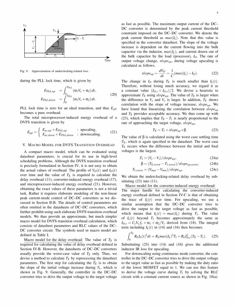
Fig. 9. Approximation of underclocking-related loss.
during the PLL lock time, which is given by
EPLL,up =∫ TPLL
0(α1Ve +α2)dt,
EPLL,down =∫ TPLL
0(α1Vs +α2)dt.
(20)
PLL lock time is zero for an ideal transition, and thus Epllbecomes a pure overhead.
The total microprocessor-induced energy overhead of aDVFS transition is given by
Eµp =
Euc,up +EPLL,up : upscaling,Euc,down +EPLL,down : downscaling. (21)
V. MACRO MODEL FOR DVFS TRANSITION OVERHEAD
A compact macro model, which can be evaluated usingdatasheet parameters, is crucial for its use in high-levelscheduling problems. Although the DVFS transition overheadis precisely formulated in Section IV, it is not easy to obtainthe actual values of overhead. The profile of VO(t) and IO(t)over time and the value of TX is required to calculate thedelay overhead (11), converter-induced energy overhead (17),and microprocessor-induced energy overhead (21). However,obtaining the exact values of these parameters is not a trivialtask. Rather it requires elaborate modeling of the non-linearpeak current-mode control of DC–DC converters as we dis-cussed in Section II-B. The details of control parameters areoften omitted in the datasheets of DC–DC converters, whichfurther prohibit using such elaborate DVFS transition overheadmodels. We thus provide an approximate, but much simplermacro model for DVFS transition overhead calculation, whichconsists of datasheet parameters and RLC values of the DC–DC converter circuit. The symbols used in macro model aredefined in Table I.
Macro model for the delay overhead: The value of TX isrequired for calculating the value of delay overhead defined inSection IV-B. However, the datasheets of DC–DC convertersusually provide the worst-case value of TX only. Thus, wedevise a method to calculate TX by reprocessing the datasheetparameters. The first step for calculating the TX is to obtainthe slope of the initial voltage increase during T1, which isshown in Fig. 9. Generally, the controller in the DC–DCconverter tries to drive the output voltage to the target voltage
as fast as possible. The maximum output current of the DC–DC converter is determined by the peak current thresholdconstraint imposed on the DC–DC converter. We denote thepeak current threshold as max(IL). Note that this value isspecified in the converter datasheet. The slope of the voltageincrease is dependent on the current flowing into the bulkcapacitor via the inductor, max(IL), and current drawn out ofthe bulk capacitor by the load (processor), IO. The rate ofoutput voltage change, slopeup, during voltage upscaling iscalculated as follows.
slopeup =dVO
dt=
1C(max(IL)− IO). (22)
The change in IO during TX is much smaller than IL(t).Therefore, without losing much accuracy, we regard it asa constant value (IO,s + IO,e)/2. We devise a heuristic toapproximate TX using slopeup. The value of TX is larger whenthe difference in Vs and Ve is larger. In addition, TX showscorrelation with the slope of voltage increase, slopeup. Wehave found that linearizing the correlation between slopeupand TX provides acceptable accuracy. We thus come up with(23), which implies that TX −T1 is nearly proportional to therate of approaching the target voltage, slopeup.
TX = T1 + slopeup ∗β. (23)
The value of β is calculated using the worst case settling timeTX , which is again specified in the datasheet. The worst caseTX occurs when the difference between the initial and finalvoltages is the largest.
T1 = (Ve−Vs)/slopeup, (24a)β = (TX ,worst −T1,worst)/slopeup,worst , (24b)
T1,worst = (Vmax−Vmin)/slopeup. (24c)
We obtain the underclocking-related delay overhead by sub-stituting (23) into (11).
Macro model for the converter-induced energy overhead:The major hurdle for calculating the converter-inducedenergy overhead defined in Section IV-C is that of obtainingthe trace of IL(t) over time. For upscaling, we use asimilar assumption that the DC–DC converter tries todrive the output to the target voltage as fast as possible,which means that IL(t) = max(IL) during T1. The valueof IL(t) beyond T1 becomes approximately the same asIO,e = CeVe fe + α1 + α2/Ve derived from (18). The integralterm including IL(t) in (14) and (16) then becomes∫ TX
0RLIL(t)2dt = RLmax(IL)
2T1 +RLI2O,e(TX −T1). (25)
Substituting (25) into (14) and (16) gives the additionalinductor IR loss for upscaling.
For downscaling using continuous mode converter, the con-troller in the DC–DC converter tries to drive the output voltageto the target value as fast as possible by making the duty ratioof the lower MOSFET equal to 1. We can use this featureto derive the voltage curve during T1 by solving the RLCcircuit with a constant current source as shown in Fig. 10(a).

9
IOCb
L
R
V1 VO
IL
(a) (b)
IOCb
VO
Fig. 10. (a) Circuit for continuous mode downscaling. (b) Circuit fordiscontinuous mode downscaling.
The traces of IL(t) and VO(t) are determined by the passivecomponents in the DC–DC converter, which are the MOSFETon-resistance, inductor, and bulk capacitor. The value of thecurrent source is assumed to be (IO,s + IO,e)/2 because itschange is not dramatic during T1. R is the summation ofwhatever resistance exists between the supply and the ground,which consists of the MOSFET on-resistance and inductorresistance. The exact trace of node voltages and inductorcurrent can be obtained by solving the following system ofnon-homogeneous differential equations.
I′LV ′1V ′O
=
0
1L
−1L
0 −RL
RL
1Cb
0 0
IL
V1VO
+
00
− IO
Cb
.
(26)The closed form solution of IL(t) and VO(t) can be obtainedby any standard method for solving a system of ordinarydifferential equations.
For downscaling using discontinuous mode converter, theinductor current is constrained to be non-negative duringnormal operation. The DC–DC converter controller generallywaits for the microprocessor to discharge the bulk capacitor.This involves solving the circuit given in Fig. 10(b).
VO(t) =Vs−IO
Ct. (27)
Sometimes the DC–DC converter drains the charge from thebulk capacitor when the voltage difference between the outputvoltage and target voltage is large. This continues until theerror becomes smaller than a certain value, e.g. 0.1 V in caseof the LTC3733 converter. For such a case, we solve both(26) and (27), and set the appropriate boundary conditions.The obtained trace of IL(t) is substituted into (16) to calculatethe additional inductor IR loss.
Macro model for the microprocessor-induced energyoverhead: The trace of VO(t) over time is required to calculatethe underclocking-related energy overhead (19). However, itis very difficult to calculate the exact value as we discussedin Section II-B. We thus make an approximation as detailedbelow.
For upscaling, we approximate the integral terms of∫VO(t)dt and
∫VO(t)2dt in (19) by calculating the area
of the two shaded triangles shown in Fig. 9. We assume
that the integral values beyond T2,∫ Tx
T2
(VO(t)−Ve)dt and∫ Tx
T2
(VO(t)2−V 2
e)
dt, add up to zero, and thus these terms
are ignored.∫ TX
0VO(t)dt ≈TXVe−
12
T1(Ve−Vs)
+12(T2−T1)Vov, (28a)∫ TX
0VO(t)2dt ≈TXV 2
e −12
T1(V 2e −V 2
s )
+12(T2−T1)
((Ve +Vov)
2−V 2e). (28b)
T1 is calculated by (24c). Vov, and T2 is calculated in asimilar way to that of calculating TX in (23). We linearize thevariations Vov, and T2−T1 according to the rate of approachingthe target voltage slopeup. Thus, the following equations hold.
Vov = γslopeup, (29a)T2 = T1 +δslopeup. (29b)
The values γ and δ are device-dependent parameters, whichdetermine the overshoot and settling time. The selection ofvalues does not affect the total DVFS transition overheadsignificantly since their effect is quite small as shown in Fig. 9.Taking (29) into account generally improves the accuracy ofthe DVFS transition overhead calculation.
For downscaling, we again use the solution of circuitsFig. 10(a) and (b) obtained from (26) and (27). The traceof output voltage, VO(t), is substituted into (19) to obtain theunderclocking-related energy loss during T1. We assume thatthe voltage ripple beyond T1 is small enough to cancel theintegral terms in Euc,down in (19).
VI. EXPERIMENTAL RESULTS
In this section, we provide experimental results for theDVFS transition overhead of microprocessors exhibiting dis-tinctive power consumption values as high as 60 W toas low as 10 mW. We emphasize that our macro modeland the experimental results are not restricted to specifictypes of microprocessors, and they are applicable to anyother microprocessors exhibiting similar amount of powerconsumption, supply voltage levels, and clock frequencies.The three representative processors we chose are Intel Core2Duo, ARM Cortex-A8, and TI MSP430. The Intel Core2 Duoprocessor shows power consumption higher than 50 W whileMSP430 shows power consumption of a few mW. We showthe accuracy and generality of the macro model by showingthe results for a wide range of processors.
A. Case 1: Intel Core2 Duo E6850 Processor
A high-fidelity DVFS transition overhead model requiresdetailed microprocessor power consumption information that
10
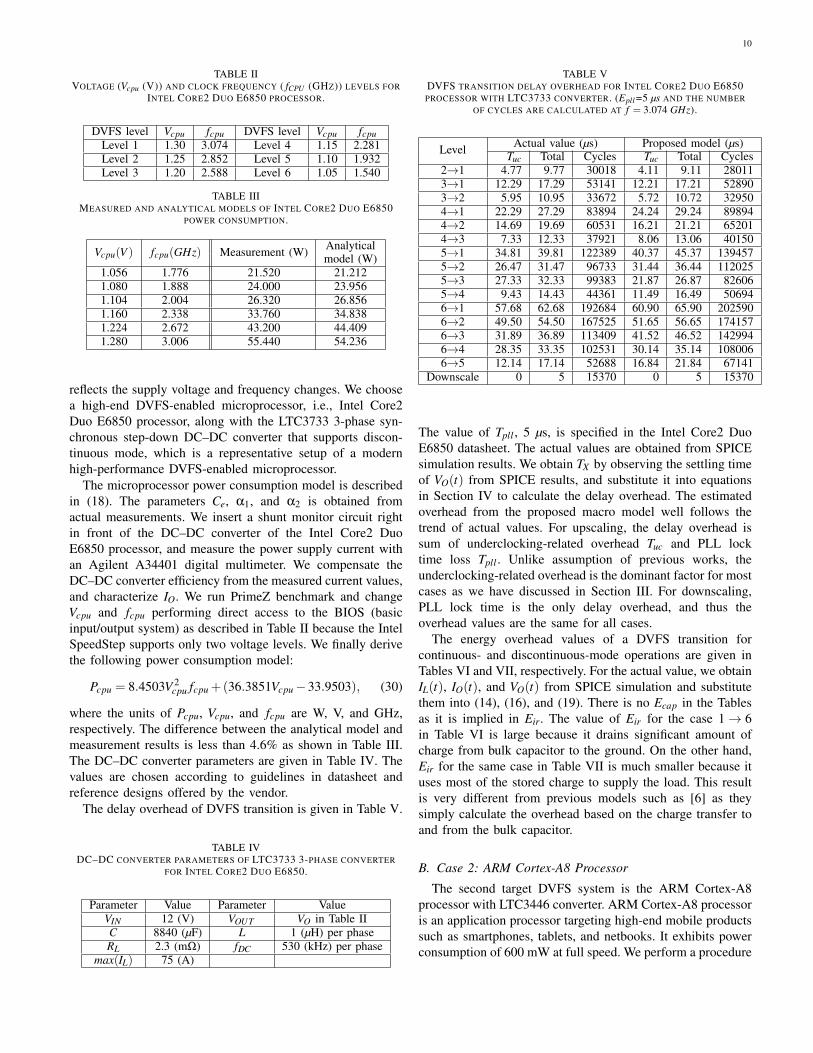
TABLE IIVOLTAGE (Vcpu (V)) AND CLOCK FREQUENCY ( fCPU (GHZ)) LEVELS FOR
INTEL CORE2 DUO E6850 PROCESSOR.
DVFS level Vcpu fcpu DVFS level Vcpu fcpuLevel 1 1.30 3.074 Level 4 1.15 2.281Level 2 1.25 2.852 Level 5 1.10 1.932Level 3 1.20 2.588 Level 6 1.05 1.540
TABLE IIIMEASURED AND ANALYTICAL MODELS OF INTEL CORE2 DUO E6850
POWER CONSUMPTION.
Vcpu(V ) fcpu(GHz) Measurement (W) Analyticalmodel (W)
1.056 1.776 21.520 21.2121.080 1.888 24.000 23.9561.104 2.004 26.320 26.8561.160 2.338 33.760 34.8381.224 2.672 43.200 44.4091.280 3.006 55.440 54.236
reflects the supply voltage and frequency changes. We choosea high-end DVFS-enabled microprocessor, i.e., Intel Core2Duo E6850 processor, along with the LTC3733 3-phase syn-chronous step-down DC–DC converter that supports discon-tinuous mode, which is a representative setup of a modernhigh-performance DVFS-enabled microprocessor.
The microprocessor power consumption model is describedin (18). The parameters Ce, α1, and α2 is obtained fromactual measurements. We insert a shunt monitor circuit rightin front of the DC–DC converter of the Intel Core2 DuoE6850 processor, and measure the power supply current withan Agilent A34401 digital multimeter. We compensate theDC–DC converter efficiency from the measured current values,and characterize IO. We run PrimeZ benchmark and changeVcpu and fcpu performing direct access to the BIOS (basicinput/output system) as described in Table II because the IntelSpeedStep supports only two voltage levels. We finally derivethe following power consumption model:
Pcpu = 8.4503V 2cpu fcpu +(36.3851Vcpu−33.9503), (30)
where the units of Pcpu, Vcpu, and fcpu are W, V, and GHz,respectively. The difference between the analytical model andmeasurement results is less than 4.6% as shown in Table III.The DC–DC converter parameters are given in Table IV. Thevalues are chosen according to guidelines in datasheet andreference designs offered by the vendor.
The delay overhead of DVFS transition is given in Table V.
TABLE IVDC–DC CONVERTER PARAMETERS OF LTC3733 3-PHASE CONVERTER
FOR INTEL CORE2 DUO E6850.
Parameter Value Parameter ValueVIN 12 (V) VOUT VO in Table IIC 8840 (µF) L 1 (µH) per phaseRL 2.3 (mΩ) fDC 530 (kHz) per phase
max(IL) 75 (A)
TABLE VDVFS TRANSITION DELAY OVERHEAD FOR INTEL CORE2 DUO E6850PROCESSOR WITH LTC3733 CONVERTER. (Epll =5 µs AND THE NUMBER
OF CYCLES ARE CALCULATED AT f = 3.074 GHz).
Level Actual value (µs) Proposed model (µs)Tuc Total Cycles Tuc Total Cycles
2→1 4.77 9.77 30018 4.11 9.11 280113→1 12.29 17.29 53141 12.21 17.21 528903→2 5.95 10.95 33672 5.72 10.72 329504→1 22.29 27.29 83894 24.24 29.24 898944→2 14.69 19.69 60531 16.21 21.21 652014→3 7.33 12.33 37921 8.06 13.06 401505→1 34.81 39.81 122389 40.37 45.37 1394575→2 26.47 31.47 96733 31.44 36.44 1120255→3 27.33 32.33 99383 21.87 26.87 826065→4 9.43 14.43 44361 11.49 16.49 506946→1 57.68 62.68 192684 60.90 65.90 2025906→2 49.50 54.50 167525 51.65 56.65 1741576→3 31.89 36.89 113409 41.52 46.52 1429946→4 28.35 33.35 102531 30.14 35.14 1080066→5 12.14 17.14 52688 16.84 21.84 67141
Downscale 0 5 15370 0 5 15370
The value of Tpll , 5 µs, is specified in the Intel Core2 DuoE6850 datasheet. The actual values are obtained from SPICEsimulation results. We obtain TX by observing the settling timeof VO(t) from SPICE results, and substitute it into equationsin Section IV to calculate the delay overhead. The estimatedoverhead from the proposed macro model well follows thetrend of actual values. For upscaling, the delay overhead issum of underclocking-related overhead Tuc and PLL locktime loss Tpll . Unlike assumption of previous works, theunderclocking-related overhead is the dominant factor for mostcases as we have discussed in Section III. For downscaling,PLL lock time is the only delay overhead, and thus theoverhead values are the same for all cases.
The energy overhead values of a DVFS transition forcontinuous- and discontinuous-mode operations are given inTables VI and VII, respectively. For the actual value, we obtainIL(t), IO(t), and VO(t) from SPICE simulation and substitutethem into (14), (16), and (19). There is no Ecap in the Tablesas it is implied in Eir. The value of Eir for the case 1→ 6in Table VI is large because it drains significant amount ofcharge from bulk capacitor to the ground. On the other hand,Eir for the same case in Table VII is much smaller because ituses most of the stored charge to supply the load. This resultis very different from previous models such as [6] as theysimply calculate the overhead based on the charge transfer toand from the bulk capacitor.
B. Case 2: ARM Cortex-A8 Processor
The second target DVFS system is the ARM Cortex-A8processor with LTC3446 converter. ARM Cortex-A8 processoris an application processor targeting high-end mobile productssuch as smartphones, tablets, and netbooks. It exhibits powerconsumption of 600 mW at full speed. We perform a procedure

11
TABLE VIDVFS TRANSITION ENERGY OVERHEAD OF LTC3733 OPERATING IN
CONTINUOUS MODE FOR INTEL CORE2 DUO E6850 PROCESSOR.
Level Actual value (µJ) Proposed model (µJ)Euc Eir Total Euc Eir Total
1→2 -2.5 -62.8 -51.9 35.4 -14.9 33.91→3 57.7 -7.1 64.0 112.7 4.2 130.21→4 152.5 177.5 343.4 202.0 119.0 335.31→5 246.0 336.8 596.2 293.7 274.2 581.31→6 329.3 680.2 1022.8 371.7 467.9 852.92→3 -11.5 -31.3 -31.3 33.0 -12.6 31.92→4 64.9 41.2 117.6 104.2 18.9 134.62→5 146.7 178.1 336.4 185.2 90.5 287.32→6 229.2 436.9 677.6 262.1 265.0 538.63→4 -1.4 -4.1 4.2 34.9 -6.7 37.93→5 65.3 110.1 185.1 94.6 28.0 132.33→6 141.1 273.4 424.3 165.7 131.3 306.74→5 3.0 22.6 33.5 32.5 -3.6 36.84→6 62.1 178.6 248.6 82.3 30.3 120.45→6 12.7 59.7 78.5 28.9 -0.3 34.72→1 29.0 378.6 420.9 16.3 352.9 382.53→1 47.1 734.3 794.7 32.4 671.2 716.93→2 43.2 373.5 428.2 40.9 335.6 388.04→1 83.1 1054.4 1150.8 91.7 951.8 1056.94→2 82.1 707.8 801.4 91.9 634.6 738.04→3 49.3 340.5 399.5 64.0 317.3 391.05→1 155.6 1352.1 1521.1 216.7 1192.6 1422.65→2 140.6 1014.1 1166.2 190.0 894.4 1095.95→3 192.9 689.5 892.1 144.9 596.3 750.95→4 58.6 315.0 381.5 85.1 298.1 391.16→1 388.6 1635.5 2037.5 423.1 1391.4 1827.86→2 331.5 1312.4 1655.4 354.9 1113.1 1479.56→3 184.9 966.4 1161.0 276.8 834.8 1121.46→4 174.1 672.6 854.6 191.9 556.6 756.36→5 61.7 276.3 344.1 103.7 278.3 388.1
End level (upscale) 1 2 3 4 5Start level (downscale)Epll (µJ) 66.8 57.7 48.6 39.5 30.4
TABLE VIIDVFS TRANSITION ENERGY OVERHEAD OF LTC3733 OPERATING INDISCONTINUOUS MODE FOR INTEL CORE2 DUO E6850 PROCESSOR.
Level Actual Value (µJ) Proposed model (µJ)Euc Eir Total Euc Eir Total
1→2 -10.6 -88.7 -85.9 0.5 -252.5 -238.71→3 74.0 -179.5 -92.1 116.3 -268.4 -138.81→4 237.9 -268.5 -17.3 268.2 -325.3 -43.81→5 376.3 -230.0 159.7 386.5 -248.2 151.71→6 478.0 -32.1 459.2 509.7 17.1 540.12→3 -14.5 -195.0 -197.9 0.5 -287.2 -275.22→4 94.3 -159.3 -53.5 124.9 -231.6 -95.22→5 248.4 -217.7 42.2 275.0 -260.4 26.22→6 375.8 -125.8 261.5 383.6 -139.1 256.03→4 1.9 -55.7 -44.1 0.5 -215.8 -205.63→5 106.0 -132.5 -16.7 138.2 -193.0 -45.23→6 266.8 -158.3 118.2 284.7 -187.0 107.44→5 10.1 -47.9 -29.9 0.5 -177.3 -168.94→6 126.0 -106.6 27.2 161.1 -153.1 15.95→6 21.5 -39.5 -11.9 0.5 -137.4 -130.8
Upscale The same as Table VI.
TABLE VIIIVOLTAGE (Vcpu (V)) AND CLOCK FREQUENCY ( fCPU (MHZ)) LEVELS FOR
ARM CORTEX-A8 PROCESSOR.
DVFS level Vcpu fcpu DVFS level Vcpu fcpuLevel 1 1.35 600 Level 4 1.10 250Level 2 1.25 550 Level 5 1.00 125Level 3 1.20 500
TABLE IXDC–DC CONVERTER PARAMETERS OF LTC3446 CONVERTER FOR ARM
CORTEX-A8.
Parameter Value Parameter ValueVIN 5 (V) VOUT VO in Table VIIIC 22 (µF) L 1 (µH)RL 1 (mΩ) fDC 2.25 (MHz)
max(IL) 1 (A)
similar to that for Intel Core2 Duo E6850 processor to modelthe power consumption of ARM Cortex-A8 processor. Theresulting equation is as follows.
Pcpu = 0.4913V 2cpu fcpu +(0.09614Vcpu−0.08187), (31)
where the units of Pcpu, Vcpu, and fcpu are W, V, and GHz,respectively. The parameters for DC–DC converters are shownin Table IX. The values are taken from datasheet and thereference design provided by the vendor.
Table X shows the DVFS transition delay overhead for thetarget system. The value of Tpll , 10 µs, is obtained from TIOMAP3530 datasheet which is based on ARM Cortex-A8.The underclocking-related overhead is higher when the changein voltage is large. Table XI shows the DVFS transition energyoverhead for the target system. Unlike LTC3733, LTC3446operates in discontinuous-mode only. There is energy gain(minus overhead) in Eir for downscaling because the inductorcurrent is fixed to 0, and no IR loss occurs when comparedwith the ideal transition.
TABLE XDVFS TRANSITION DELAY OVERHEAD OF ARM CORTEX-A8 WITH
LTC3446 CONVERTER. (Tpll = 10µs AND THE NUMBER OF CYCLES ISCALCULATED AT f = 600 MHz)
Level Actual (µs) Model (µs)Tuc Total Cycles Tuc Total Cycles
2→1 4.3 14.3 8586 5.5 15.5 92863→1 11.5 21.5 12912 12.2 22.2 133033→2 4.5 14.5 8685 6.4 16.4 98424→1 60.2 70.2 42124 54.6 64.6 387484→2 46.3 56.3 33765 49.9 59.9 359464→3 39.0 49.0 29378 44.8 54.8 329095→1 119.8 129.8 77890 81.0 91.0 545815→2 106.9 116.9 70117 77.6 87.6 525395→3 104.0 114.0 68402 74.0 84.0 504235→4 23.1 33.1 19873 47.6 57.6 34549

12
TABLE XIDVFS TRANSITION ENERGY OVERHEAD FOR ARM CORTEX-A8 WITH
LTC3446 CONVERTER.
LevelActual Value Proposed model
Euc Eir Total Euc Eir Total(nJ) (nJ) (nJ) (nJ) (nJ) (nJ)
1→2 187 -939 -350 145 -683 -1361→3 297 -1296 -664 509 -1140 -2961→4 2056 -1184 1062 2138 -1158 11711→5 3960 -804 3274 3684 -802 30002→3 73 -675 -266 113 -514 -662→4 1090 -836 445 1179 -814 5562→5 2452 -602 1968 2369 -599 18893→4 429 -548 72 561 -534 2183→5 1385 -435 1069 1430 -434 11154→5 113 -131 101 175 -128 1662→1 242 2285 3006 256 2422 31573→1 435 4403 5317 410 4369 52583→2 223 1827 2452 287 2039 27294→1 2385 7943 10808 2243 7579 103004→2 1637 5392 7432 1847 5558 78074→3 1168 3153 4656 1468 3789 55925→1 5396 9278 15154 3540 8853 128735→2 4014 6580 10996 2935 6965 103025→3 3239 4399 7973 2397 5312 80445→4 3309 2529 6029 943 1771 2905
End level (upscale) 1 2 3 4Start level (downscale)Epll (nJ) 402 335 191 119
TABLE XIIVOLTAGE (Vcpu (V)) AND CLOCK FREQUENCY ( fCPU (MHZ)) LEVELS FOR
TI MSP430 MICROCONTROLLER.
DVFS level Vcpu fcpu DVFS level Vcpu fcpuLevel 1 3.3 8 Level 4 2.175 5Level 2 2.925 7 Level 5 1.8 4Level 3 2.55 6
C. Case 3: TI MSP430 Microcontroller
The third target system is the TI MSP430 microcontroller.TI MSP430 is a microcontroller used for ultra low-powerembedded systems such as wireless sensor nodes. The powerconsumption of the TI MSP430 microcontroller is at most10.1 mW. A procedure similar to that for ARM Cortex-A8 isperformed to obtain the following power model.
Pcpu = 0.1128V 2cpu fcpu +(0.1738Vcpu−0.2832), (32)
TABLE XIIIDC–DC CONVERTER PARAMETERS OF LTC3620 CONVERTER FOR TI
MSP430 MICROCONTROLLER.
Parameter Value Parameter ValueVIN 3.6 (V) VOUT VO in Table XIIC 1 (µF) L 22 (µH)RL 1 (mΩ) fDC Variable (PFM)
max(IL) 15 (mA)
TABLE XIVDVFS DELAY OVERHEAD OF DC–DC CONVERTERS FOR TI MSP430
MICROCONTROLLER WITH LTC3620. (THE NUMBER OF CYCLES ISCALCULATED AT f = 8 MHz)
Level Actual value Proposed modelTuc (µs) Cycles Tuc (µs) Cycles
2→1 79.4 635 214 17123→1 382.3 3058 478.4 38273→2 103.4 827 254.3 20354→1 706 5648 786.2 62904→2 477.7 3822 562.3 44994→3 139 1112 306.7 24535→1 1116.1 8929 1132 90565→2 879.1 7033 917 73365→3 623.8 4990 671.8 53745→4 278.5 2228 378.2 3026
where the units of Pcpu, Vcpu, and fcpu are mW, V, andMHz, respectively. We use LTC3620 converter to power thetarget processor. The parameters for the DC–DC converter arereported in Table XIII.
Table XIV shows the DVFS transition delay overhead forthe target system. There is no overhead due to PLL lock timeTpll because TI MSP430 uses digitally controlled oscillator(DCO) instead of PLL, which is a improved variation of VCO.The underclocking-related overhead Tuc is the only delayoverhead for TI MSP430 microcontroller. Table XV showsthe DVFS transition energy overhead for the target system.LTC3620 is designed for low-power applications. It is PFMcontrolled and operates in discontinuous mode only. The IRloss for TI MSP430 processor is very small due to small loadcurrent. The underclocking-related overhead is relatively largebecause of the long voltage settling time due to simple controlmethod.
The result of the proposed model is inaccurate for somecases when the difference in the initial and final voltage levelsis small because our model does not take into account all thedetails during the voltage transition period. However, the resultof the proposed model follows the general trend well.
VII. IMPACT OF DVFS TRANSITION OVERHEAD:DYNAMIC THERMAL MANAGEMENT EXAMPLE
In this section, we show how much DVFS transitionoverhead impacts on overall system performance and energyconsumption when we perform dynamic thermal management(DTM). DVFS is a very useful control knob for dynamicthermal management (DTM) [25], [26]. DTM techniquesbased on PID control method usually use the time quantumof the operating system as the minimum time granularity. Thetime quantum of operating system is in the range of a fewmilliseconds. On the contrary, the thermal RC time constant ofa processor is much larger than the time quantum of operatingsystems. Although the two time constants differ in magnitude,the DVFS transition occurs much more frequently than thethermal RC time constant when the chip temperature is nearthe target temperature.

13
TABLE XVDVFS TRANSITION ENERGY OVERHEAD OF TI MSP430
MICROCONTROLLER WITH LTC3620.
LevelActual Value Proposed model
Euc Eir Total Euc Eir Total(nJ) (nJ) (nJ) (nJ) (nJ) (nJ)
1→2 720.9 -4.1 716.8 649.2 -4.5 644.71→3 2565.6 -6.8 2558.8 2547.8 -7.3 2540.51→4 5413.9 -8.3 5405.6 5619.8 -8.5 5611.31→5 9116.3 -8.4 9107.9 9802.4 -8.6 9793.82→3 701.0 -2.4 698.6 652.1 -3.4 648.72→4 2515.6 -5.0 2510.6 2562.1 -5.3 2556.82→5 5371.7 -5.8 5365.9 5674.2 -5.9 5668.33→4 694.0 -2.3 691.7 659.9 -2.4 657.53→5 2530.7 -3.5 2527.2 2610.0 -3.6 2606.44→5 689.0 -1.5 687.5 680.4 -1.6 678.82→1 60.9 75.6 136.5 418.2 56.3 474.53→1 300.8 151.8 452.6 188.6 108.2 296.83→2 29.2 72.1 101.3 374.6 54.1 428.74→1 177.7 197.0 374.7 -57.8 157.8 1004→2 245.6 140.5 386.1 209.4 104.5 313.94→3 39.4 67.0 106.4 313.2 52.3 365.55→1 -18.1 232.0 213.9 -232.1 203.0 -29.15→2 108.4 178.1 286.5 47.7 152.2 199.95→3 204.0 125.4 329.4 195.8 101.5 297.35→4 75.9 65.3 141.2 240.0 50.7 290.7
0 1 2 3 4 50
1
2
3
4
Time (ms)
Ove
rhea
d (%
)
Energy overheadDelay overhead
Fig. 11. Energy and delay overhead of PID control based DTM for IntelCore2 Duo E6850 processor according to time granularity of DTM.
We implement a PID control-based DTM scheme in MAT-LAB/Simulink environment. Parameters of the PID controllerare determined by a tuner embedded in MATLAB/Simulink.The thermal resistance from the chip to the ambient isR = 0.7 K/W and thermal capacitance of the chip is C =140.3 J/K, which is the same as [25]. The thermal RCconstant is 98.21 seconds. Fig. 11 shows the delay and energyoverhead of DVFS according to the time granularity of DTMfor Intel Core2 Duo E6850 processor. The results show thatwe should avoid using time quantum value below 1 ms forperformance and energy efficiency. The energy and delayoverhead is comparable to the scheduling overhead and contextswitching overhead of operating systems, which take about0.4% to 1.6% in general purpose operating systems [27].
VIII. CONCLUSIONS
Dynamic voltage and frequency (DVFS) scaling is widelyused for energy saving and thermal management nowadays.
Understanding correct DVFS transition overhead is crucialin achieving the maximum power gain and thermal stability.In fact, DVFS transition overhead is comparable to contextswitching overhead in modern microprocessors. However,DVFS transition overhead has not been properly dealt so fardue to absence of correct and accurate models.
This paper is the first paper that introduces correct andaccurate DVFS transition overhead models. We show thatenergy to charge and discharge the bulk capacitor in the DC-DC converter, which was regarded as the major source ofoverhead, is not true overhead. Instead, we introduce energyand delay overhead caused by microprocessor underclockingand additional current through the inductor. This paper pro-vides comprehensive solutions for the models, but the derivedmodel is somewhat complicated for system engineers. We alsoprovide succinct macromodels while maintaining reasonableaccuracy. Finally, we summarize DVFS transition overheadvalues of three representative microprocessors for high-end,embedded and ultra low-power applications, such as IntelCore2 Duo E6850, Cortex-A8 and TI MSP430 so that somesoftware programmers may simply use the numbers.
REFERENCES
[1] Intel Core2 Extreme Processor QX9000 and Intel Core2 Quad ProcessorQ9000, Q9000S, Q8000 and Q8000S Series Datasheet, 2009.
[2] Y.-H. Lu and G. De Micheli, “Comparing system level power manage-ment policies,” Design Test of Computers, IEEE, vol. 18, no. 2, pp. 10–19, mar/apr 2001.
[3] T. Ishihara and H. Yasuura, “Voltage scheduling problem fordynamically variable voltage processors,” in Proceedings of the 1998international symposium on Low power electronics and design, ser.ISLPED ’98. New York, NY, USA: ACM, 1998, pp. 197–202.[Online]. Available: http://doi.acm.org/10.1145/280756.280894
[4] W. Kim, J. Kim, and S. L. Min, “Preemption-aware dynamic voltagescaling in hard real-time systems,” in Low Power Electronics andDesign, 2004. ISLPED ’04. Proceedings of the 2004 InternationalSymposium on, aug. 2004, pp. 393 – 398.
[5] Z. Cao, B. Foo, L. He, and M. van der Schaar, “Optimality andimprovement of dynamic voltage scaling algorithms for multimediaapplications,” in Proceedings of the 45th annual Design AutomationConference, ser. DAC ’08. New York, NY, USA: ACM, 2008, pp. 179–184. [Online]. Available: http://doi.acm.org/10.1145/1391469.1391516
[6] T. D. Burd and R. W. Brodersen, “Design issues for dynamicvoltage scaling,” in Proceedings of the 2000 international symposiumon Low power electronics and design, ser. ISLPED ’00. NewYork, NY, USA: ACM, 2000, pp. 9–14. [Online]. Available:http://doi.acm.org/10.1145/344166.344181
[7] S. M. Martin, K. Flautner, T. Mudge, and D. Blaauw, “Combineddynamic voltage scaling and adaptive body biasing for lower powermicroprocessors under dynamic workloads,” in Proceedings of the2002 IEEE/ACM international conference on Computer-aided design,ser. ICCAD ’02. New York, NY, USA: ACM, 2002, pp. 721–725.[Online]. Available: http://doi.acm.org/10.1145/774572.774678
[8] X. Zhang, A. Bermak, and F. Boussaid, “Dynamic voltage and frequencyscaling for low-power multi-precision reconfigurable multiplier,” inCircuits and Systems (ISCAS), Proceedings of 2010 IEEE InternationalSymposium on, 30 2010-june 2 2010, pp. 45 –48.
[9] M. Schmitz, B. Al-Hashimi, and P. Eles, “Energy-efficientmapping and scheduling for dvs enabled distributed embeddedsystems,” in Proceedings of the conference on Design, automationand test in Europe, ser. DATE ’02. Washington, DC, USA:IEEE Computer Society, 2002, pp. 514–. [Online]. Available:http://dl.acm.org/citation.cfm?id=882452.874328
[10] Voltage Regulator Module (VRM) and Enterprise Voltage Regulator-Down (EVRD) 11.1, 2009.
14
[11] J. Park, D. Shin, M. Pedram, and N. Chang, “Accurate modelingand calculation of delay and energy overheads of dynamic voltagescaling in modern high-performance microprocessors,” in Proceedingsof Proceedings of IEEE/ACM International Symposium on Low PowerElectronics and Design (ISLPED), August 2010, pp. 419–424.
[12] R. Ridley, “A new, continuous-time model for current-mode control[power convertors],” Power Electronics, IEEE Transactions on, vol. 6,no. 2, pp. 271 –280, apr 1991.
[13] B. Bryant and M. Kazimierczuk, “Modeling the closed-current loop ofpwm boost dc-dc converters operating in ccm with peak current-modecontrol,” Circuits and Systems I: Regular Papers, IEEE Transactions on,vol. 52, no. 11, pp. 2404 – 2412, nov. 2005.
[14] LTSPICE. www.linear.com.[15] T. Sakurai and A. Newton, “Alpha-power law mosfet model and its
applications to cmos inverter delay and other formulas,” Solid-StateCircuits, IEEE Journal of, vol. 25, no. 2, pp. 584 –594, apr 1990.
[16] “Introduction to intel core duo processor architecture,” in Intel Technol-ogy Journal, vol. 10, 2006, pp. 89 –97.
[17] S. Lee and T. Sakurai, “Run-time voltage hopping for low-power real-time systems,” in Design Automation Conference, 2000. Proceedings2000. 37th, 2000, pp. 806 –809.
[18] A. Bashir, J. Li, K. Ivatury, N. Khan, N. Gala, N. Familia, andZ. Mohammed, “Fast lock scheme for phase-locked loops,” in CustomIntegrated Circuits Conference, 2009. CICC ’09. IEEE, sept. 2009, pp.319 –322.
[19] J. Pouwelse, K. Langendoen, and H. Sips, “Dynamic voltage scalingon a low-power microprocessor,” in Proceedings of the 7th annualinternational conference on Mobile computing and networking, ser.MobiCom ’01. New York, NY, USA: ACM, 2001, pp. 251–259.[Online]. Available: http://doi.acm.org/10.1145/381677.381701
[20] C. Lichtenau, M. Ringler, T. Pfluger, S. Geissler, R. Hilgendorf,J. Heaslip, U. Weiss, P. Sandon, N. Rohrer, E. Cohen, and M. Canada,“Powertune: advanced frequency and power scaling on 64b powerpcmicroprocessor,” in Solid-State Circuits Conference, 2004. Digest ofTechnical Papers. ISSCC. 2004 IEEE International, feb. 2004, pp. 356– 357 Vol.1.
[21] B. Mochocki, X. S. Hu, and G. Quan, “A realistic variable voltagescheduling model for real-time applications,” in Proceedings of the2002 IEEE/ACM international conference on Computer-aided design,ser. ICCAD ’02. New York, NY, USA: ACM, 2002, pp. 726–731.[Online]. Available: http://doi.acm.org/10.1145/774572.774679
[22] P. Schaumont, B.-C. C. Lai, W. Qin, and I. Verbauwhede, “Coopera-tive multithreading on embedded multiprocessor architectures enablesenergy-scalable design,” in Design Automation Conference, 2005. Pro-ceedings. 42nd, june 2005, pp. 27 – 30.
[23] D. Shin and J. Kim, “Optimizing intratask voltage scheduling usingprofile and data-flow information,” Computer-Aided Design of IntegratedCircuits and Systems, IEEE Transactions on, vol. 26, no. 2, pp. 369 –385, feb. 2007.
[24] P. Pillai and K. G. Shin, “Real-time dynamic voltage scaling for low-power embedded operating systems,” in Proceedings of the eighteenthACM symposium on Operating systems principles, ser. SOSP ’01.New York, NY, USA: ACM, 2001, pp. 89–102. [Online]. Available:http://doi.acm.org/10.1145/502034.502044
[25] S. Zhang and K. Chatha, “Approximation algorithm for the temperature-aware scheduling problem,” in Computer-Aided Design, 2007. ICCAD2007. IEEE/ACM International Conference on, nov. 2007, pp. 281 –288.
[26] K. Skadron, M. R. Stan, K. Sankaranarayanan, W. Huang,S. Velusamy, and D. Tarjan, “Temperature-aware microarchitecture:Modeling and implementation,” ACM Trans. Archit. Code Optim.,vol. 1, no. 1, pp. 94–125, Mar. 2004. [Online]. Available:http://doi.acm.org/10.1145/980152.980157
[27] D. Tsafrir, “The context-switch overhead inflicted by hardwareinterrupts (and the enigma of do-nothing loops),” in Proceedingsof the 2007 workshop on Experimental computer science, ser.ExpCS ’07. New York, NY, USA: ACM, 2007. [Online]. Available:http://doi.acm.org/10.1145/1281700.1281704