abstract - university of washington
TRANSCRIPT

ABSTRACT
KEPHART, JEREMY D. Method of Evaluating the effect of HPGe Design on the Sensitivityof Physics Experiments. (Under the direction of Dr. Albert Young).
Motivated by planned double beta decay experiments in 76Ge I describe a com-
putational model for the electric fields of solid state diode detectors and the subsequent
charge transport. Aspects of detector performance determined by the impurity charge con-
centration are explored in a series of measurements of comparable “point contact” p-type
germanium detectors and compared to our computational model.
In particular, we measure the capacitance of the germanium detector as a function
of the bias voltage to determine the free parameters in a three parameter model of the
impurity charge density, effectively mapping out the density at all points within the detector
volume. We then use our impurity charge density map to refine the sensitivity of pulse shape
analysis applied to various classes of physics events detected in the crystal. When possible,
the impact of our refinements on a figure-of-merit for double-beta decay experiments is
described.
Method of Evaluating the effect of HPGe Design on the Sensitivity of PhysicsExperiments
byJeremy Dale Kephart
A dissertation submitted to the Graduate Faculty ofNorth Carolina State University
in partial fullfillment of therequirements for the Degree of
Doctor of Philosophy
Physics
Raleigh, North Carolina
2009
APPROVED BY:
Dr. Paul Huffman Dr. Robert White
Dr. Albert Young Dr. Christopher GouldChair of Advisory Committee

v
TABLE OF CONTENTS
LIST OF TABLES. . . . . . . . . . . . . . . . . . . . . . . . . . . . . . . . . . . . . . . . . . . . . . . . . . . . . . . . viii
LIST OF FIGURES . . . . . . . . . . . . . . . . . . . . . . . . . . . . . . . . . . . . . . . . . . . . . . . . . . . . . . ix
1 Motivation . . . . . . . . . . . . . . . . . . . . . . . . . . . . . . . . . . . . . . . . . . . . . . . . . . . . . . . . . . . . 11.1 Overview . . . . . . . . . . . . . . . . . . . . . . . . . . . . . . . . . . . . . 11.2 Introduction . . . . . . . . . . . . . . . . . . . . . . . . . . . . . . . . . . . . 3
1.2.1 Neutrinos . . . . . . . . . . . . . . . . . . . . . . . . . . . . . . . . . 31.3 Motivation . . . . . . . . . . . . . . . . . . . . . . . . . . . . . . . . . . . . 4
1.3.1 IGEX . . . . . . . . . . . . . . . . . . . . . . . . . . . . . . . . . . . 41.3.2 Heidelberg-Moscow . . . . . . . . . . . . . . . . . . . . . . . . . . . . 51.3.3 GERDA . . . . . . . . . . . . . . . . . . . . . . . . . . . . . . . . . . 51.3.4 Majorana . . . . . . . . . . . . . . . . . . . . . . . . . . . . . . . . . 61.3.5 Necessary advances addressed by this work . . . . . . . . . . . . . . 61.3.6 Wrapping it all up . . . . . . . . . . . . . . . . . . . . . . . . . . . . 9
1.4 Scope of this work . . . . . . . . . . . . . . . . . . . . . . . . . . . . . . . . 9
2 Fundamentals of radiation interaction with high purity germanium detec-tors . . . . . . . . . . . . . . . . . . . . . . . . . . . . . . . . . . . . . . . . . . . . . . . . . . . . . . . . . . . . . . . . . . . 112.1 Introduction . . . . . . . . . . . . . . . . . . . . . . . . . . . . . . . . . . . . 112.2 The Detection Process . . . . . . . . . . . . . . . . . . . . . . . . . . . . . . 122.3 Photon Interactions with Matter . . . . . . . . . . . . . . . . . . . . . . . . 12
2.3.1 Compton Scattering . . . . . . . . . . . . . . . . . . . . . . . . . . . 132.3.2 Photoelectric Absorption . . . . . . . . . . . . . . . . . . . . . . . . 142.3.3 Pair Production . . . . . . . . . . . . . . . . . . . . . . . . . . . . . 142.3.4 Other forms of interactions . . . . . . . . . . . . . . . . . . . . . . . 15
2.4 HPGe as a radiation detector . . . . . . . . . . . . . . . . . . . . . . . . . . 152.4.1 Charge Carrier Mobility . . . . . . . . . . . . . . . . . . . . . . . . . 182.4.2 Statistics of charge collection . . . . . . . . . . . . . . . . . . . . . . 202.4.3 Charge Impurity . . . . . . . . . . . . . . . . . . . . . . . . . . . . . 22
2.5 Electronics . . . . . . . . . . . . . . . . . . . . . . . . . . . . . . . . . . . . 25
3 Charge Transport Simulation . . . . . . . . . . . . . . . . . . . . . . . . . . . . . . . . . . . . . . . . . . 283.1 Introduction . . . . . . . . . . . . . . . . . . . . . . . . . . . . . . . . . . . . 283.2 Charge Transport Code . . . . . . . . . . . . . . . . . . . . . . . . . . . . . 28
3.2.1 Field Solutions . . . . . . . . . . . . . . . . . . . . . . . . . . . . . . 293.2.2 Charge Transport Dynamics . . . . . . . . . . . . . . . . . . . . . . . 333.2.3 Pulse Processing . . . . . . . . . . . . . . . . . . . . . . . . . . . . . 343.2.4 Verification and Validation . . . . . . . . . . . . . . . . . . . . . . . 35

vi
3.3 Charge Impurity Profile . . . . . . . . . . . . . . . . . . . . . . . . . . . . . 36
4 Single from Multiple Site Rejection . . . . . . . . . . . . . . . . . . . . . . . . . . . . . . . . . . . . 404.1 Why we need it . . . . . . . . . . . . . . . . . . . . . . . . . . . . . . . . . . 404.2 Statistical Moments . . . . . . . . . . . . . . . . . . . . . . . . . . . . . . . 44
4.2.1 Statistical Moments properties . . . . . . . . . . . . . . . . . . . . . 444.3 Pulse Shape Discrimination . . . . . . . . . . . . . . . . . . . . . . . . . . . 48
4.3.1 Introduction . . . . . . . . . . . . . . . . . . . . . . . . . . . . . . . 484.3.2 Aalseth PSD Method . . . . . . . . . . . . . . . . . . . . . . . . . . 484.3.3 Analytical Model for PSD . . . . . . . . . . . . . . . . . . . . . . . . 534.3.4 Velocity and the PSD parameter space . . . . . . . . . . . . . . . . . 544.3.5 Notes on PSD . . . . . . . . . . . . . . . . . . . . . . . . . . . . . . . 56
4.4 Figure of Merit . . . . . . . . . . . . . . . . . . . . . . . . . . . . . . . . . . 58
5 A P-type Modified Electrode Detector: Overview of Detector Properties 605.1 Introduction . . . . . . . . . . . . . . . . . . . . . . . . . . . . . . . . . . . . 605.2 Motivation for the P-type Detector Geometry . . . . . . . . . . . . . . . . . 615.3 Method . . . . . . . . . . . . . . . . . . . . . . . . . . . . . . . . . . . . . . 655.4 Results . . . . . . . . . . . . . . . . . . . . . . . . . . . . . . . . . . . . . . . 695.5 Conclusion . . . . . . . . . . . . . . . . . . . . . . . . . . . . . . . . . . . . 73
6 Determination of the Impurity Profile for a PPC Detector . . . . . . . . . . . . . 756.1 Introduction . . . . . . . . . . . . . . . . . . . . . . . . . . . . . . . . . . . . 756.2 Physics of HPGe Detector Capacitance . . . . . . . . . . . . . . . . . . . . . 77
6.2.1 Electronic noise and capacitance . . . . . . . . . . . . . . . . . . . . 806.3 Capacitance Measurement . . . . . . . . . . . . . . . . . . . . . . . . . . . . 816.4 Impurity profile from Capacitance . . . . . . . . . . . . . . . . . . . . . . . 836.5 Efficiency Method for Impurity Profile . . . . . . . . . . . . . . . . . . . . . 856.6 Four point Resistance Measurement . . . . . . . . . . . . . . . . . . . . . . 876.7 Pulse Shape Library from a Scan . . . . . . . . . . . . . . . . . . . . . . . . 896.8 Conclusion . . . . . . . . . . . . . . . . . . . . . . . . . . . . . . . . . . . . 90
7 Position Resolution . . . . . . . . . . . . . . . . . . . . . . . . . . . . . . . . . . . . . . . . . . . . . . . . . . . . 917.1 Overview . . . . . . . . . . . . . . . . . . . . . . . . . . . . . . . . . . . . . 917.2 Factors affecting position resolution . . . . . . . . . . . . . . . . . . . . . . 91
7.2.1 Intrinsic Factors . . . . . . . . . . . . . . . . . . . . . . . . . . . . . 917.2.2 Technical Factors . . . . . . . . . . . . . . . . . . . . . . . . . . . . . 937.2.3 Consequences . . . . . . . . . . . . . . . . . . . . . . . . . . . . . . . 95
7.3 Effect of Anisotropic Drift Velocity . . . . . . . . . . . . . . . . . . . . . . . 967.4 Effect of Finite Carrier Lifetimes . . . . . . . . . . . . . . . . . . . . . . . . 1027.5 Optimizing a Geometry . . . . . . . . . . . . . . . . . . . . . . . . . . . . . 106

vii
8 Conclusion . . . . . . . . . . . . . . . . . . . . . . . . . . . . . . . . . . . . . . . . . . . . . . . . . . . . . . . . . . . . 1128.1 Overview . . . . . . . . . . . . . . . . . . . . . . . . . . . . . . . . . . . . . 1128.2 Extension of this work to future 0νββ decay experiments . . . . . . . . . . 114
Bibliography . . . . . . . . . . . . . . . . . . . . . . . . . . . . . . . . . . . . . . . . . . . . . . . . . . . . . . . . . . . . . 118
Appendices . . . . . . . . . . . . . . . . . . . . . . . . . . . . . . . . . . . . . . . . . . . . . . . . . . . . . . . . . . . . . . . 130Appendix A. Shockely Ramo theorem for calculation . . . . . . . . . . . . . 131

viii
LIST OF TABLES
Table 1.1 Characterization of the 5 enriched Heidelberg-Moscow HPGe detectors [1]. . . 5
Table 2.1 Common shallow donors and acceptors that can be used in high purity ger-manium semiconductors [2]. . . . . . . . . . . . . . . . . . . . . . . . . . . . . . . . . . . . . . . . . . . . . . . . . . . . . . . 23
Table 2.2 Segregation coefficients for elements in germanium as reported by Trumbore[3].The elements U,Th and K are not known but of particular interest as sources ofbackground in HPGe detectors. . . . . . . . . . . . . . . . . . . . . . . . . . . . . . . . . . . . . . . . . . . . . . . . . . . . 25
Table 3.1 Coefficients for the velocity equation Eq. 3.1 from [4]. . . . . . . . . . . . . . . . . . . . . . . 34
Table 7.1 Mass attenuation Coefficients, density, and thicknesses for the materials usedin the measurement [5]. Dead layer thicknesses are typically ”several hunderedmicrometers”[6]. . . . . . . . . . . . . . . . . . . . . . . . . . . . . . . . . . . . . . . . . . . . . . . . . . . . . . . . . . . . . . . . . . . 99

ix
LIST OF FIGURES
Figure 2.1 Representation of the diamond lattice structure of high purity germanium. 16
Figure 2.2 The band structure of Germanium. Used with permission [2]. . . . . . . . . . . . . . 16
Figure 2.3 The range of an electron of given energy in high purity germanium. . . . . . . . 17
Figure 2.4 Comparison of the magnitude of the electric field for a coaxial HPGe detectorwith and without a charged impurities. The radius goes from an inner radius of 1.5mm to an outer radius of 14 mm. The impurity density was given as constant at0.0003 C/m3. The black line illustrate the electric field at depletion at 100 Voltsup to 150 Volts applied to the contact. The red line shows the electric field withoutcharged impurities at 150 volts. . . . . . . . . . . . . . . . . . . . . . . . . . . . . . . . . . . . . . . . . . . . . . . . . . . 24
Figure 2.5 Impurity profile of a germanium ingot [7]. The crystal growth seed is locatedat the 0 % end of the crystal. . . . . . . . . . . . . . . . . . . . . . . . . . . . . . . . . . . . . . . . . . . . . . . . . . . . . 26
Figure 3.1 A simple HPGe detector showing cylindrical, spherical and conic shapedregions. . . . . . . . . . . . . . . . . . . . . . . . . . . . . . . . . . . . . . . . . . . . . . . . . . . . . . . . . . . . . . . . . . . . . . . . . . . 30
Figure 3.2 Illustration of how congruent solid geometry descriptions can represent com-plex geometries. Starting with a simple cylinder on the right, we can apply a sub-traction of another smaller cylinder to produce a coaxial cylinder. We can thenuse a union to join another cylinder to the top to generate a semi coaxial detectorshape. . . . . . . . . . . . . . . . . . . . . . . . . . . . . . . . . . . . . . . . . . . . . . . . . . . . . . . . . . . . . . . . . . . . . . . . . . . . 31
Figure 3.3 Illustration of how a cylinder super-imposed on a Cartesian grid. In red arethe grid points of a regular Cartesian grid. With the cylinder superimposed theblue shows the volume of our effective solution. . . . . . . . . . . . . . . . . . . . . . . . . . . . . . . . . . . 32
Figure 3.4 This figure demonstrates the relationship between each grid point and thesuper-imposed surface grid point. The Blue connections are pointers from each gridpoint to its neighbor. The Red connections are pointers to the surface grid pointpotential. These links have the correct distance to the correct nearest neighbor.These surface elements can be understood as the superposition of two different gridsystems. These two grids allow us the ease of a regular Cartesian grid while usingthe surface grid to correctly enforce boundary conditions. The ability to buildthe surface grid in any non-uniform way allows for the construction of complexgeometries. . . . . . . . . . . . . . . . . . . . . . . . . . . . . . . . . . . . . . . . . . . . . . . . . . . . . . . . . . . . . . . . . . . . . . . 33

x
Figure 3.5 The potential of a true cylindrical coaxial HPGe from simulation comparedto the analytical solution [6]. . . . . . . . . . . . . . . . . . . . . . . . . . . . . . . . . . . . . . . . . . . . . . . . . . . . . . 37
Figure 3.6 Comparison between simulated energy depositions uniformly distributedthrough an HPGe detector and the energy given after charge transport simula-tion. This type of systematic test shows that the energy is preserved across thecrystal volume. This type of test also shows that charge is conserved as well. . . . . . 38
Figure 4.1 The electron range in HPGe versus initial energy. The solid horizontal lineshows the 1 mm electron path length close to 0.9 MeV. . . . . . . . . . . . . . . . . . . . . . . . . . . 43
Figure 4.2 Theoretical PSD parameter space with color indicating the distance betweenmultiple interactions. . . . . . . . . . . . . . . . . . . . . . . . . . . . . . . . . . . . . . . . . . . . . . . . . . . . . . . . . . . . . 49
Figure 4.3 A current pulse with the 10% to 10% of the maximum enclosed in a box.The timming points needed are the start time, the end time and the time directlyin the middle of these two, called the mid time. . . . . . . . . . . . . . . . . . . . . . . . . . . . . . . . . . . 50
Figure 4.4 The front back area and the half back area as measured from a current pulse. 51
Figure 4.5 The PSD line for single site events as the interaction point moves alongthe radius. The different lines indicate the effect of different combinations of driftvelocities for electrons and hole respectively. . . . . . . . . . . . . . . . . . . . . . . . . . . . . . . . . . . . . . 55
Figure 5.1 This notional diagram shows the comparison of an ordinary p-type detector(left) and a p-type point contact detector (right) showing a dead layer (dark), bulkp-type material (light), and an implanted contact on the central hole (thinned). . . 62
Figure 5.2 Impurity profile of a germanium ingot [7]. The crystal growth seed is locatedat the 0 percent end of the crystal. . . . . . . . . . . . . . . . . . . . . . . . . . . . . . . . . . . . . . . . . . . . . . . . 64
Figure 5.3 Simplified schematic of a typical HPGe preamplifier circuit focusing on thecontributions to the front end capacitance. The PPC preamp may or may not havea Feedback loop in the circuit. . . . . . . . . . . . . . . . . . . . . . . . . . . . . . . . . . . . . . . . . . . . . . . . . . . . 67
Figure 5.4 Calculated depletion voltage for given values of minimum charge impurityand charge impurity profile. Dark to light shading represents low to high depletionvoltage respectively. The computation was cutoff at 5000 V. The darkest shadingrepresents 0 V. Imposing a lower bound of 1000 V would only remove a small regionvery close to the origin. . . . . . . . . . . . . . . . . . . . . . . . . . . . . . . . . . . . . . . . . . . . . . . . . . . . . . . . . . . 70
Figure 5.5 Calculated charge collection time surface parameterized by A and B. Theprototype PPC showed a charge collection of up to 700 ns. . . . . . . . . . . . . . . . . . . . . . . . 72

xi
Figure 5.6 Capacitance versus bias voltage for the prototype PPC [8] compared withsimulation. . . . . . . . . . . . . . . . . . . . . . . . . . . . . . . . . . . . . . . . . . . . . . . . . . . . . . . . . . . . . . . . . . . . . . . 73
Figure 6.1 Effects of a reverse bias on a p-n junction. As the voltage increases, theamount of the charge in both the acceptor and donor regions increase by the regionsincreasing in volume. . . . . . . . . . . . . . . . . . . . . . . . . . . . . . . . . . . . . . . . . . . . . . . . . . . . . . . . . . . . . 79
Figure 6.2 Capacitance measurement of a HPGe detector using injected voltage pulse,compared to 60Co 1332 keV peak. . . . . . . . . . . . . . . . . . . . . . . . . . . . . . . . . . . . . . . . . . . . . . . . . 83
Figure 6.3 Iterating over a parameter space of the charge impurity profile, a fit to thecapacitance was found.. . . . . . . . . . . . . . . . . . . . . . . . . . . . . . . . . . . . . . . . . . . . . . . . . . . . . . . . . . . 85
Figure 6.4 The Number of counts for a collimated 60Co source placed at four differentheights versus the applied bias voltage of the University of Chicago PPC detector.As the applied voltage increases, the active volume increases thus the number ofcounts should increase proportionately. . . . . . . . . . . . . . . . . . . . . . . . . . . . . . . . . . . . . . . . . . . . 87
Figure 7.1 Spectra for a 120% HPGe detector for a colimated 57Co source at differentangles to the front of the detector. . . . . . . . . . . . . . . . . . . . . . . . . . . . . . . . . . . . . . . . . . . . . . . . 98
Figure 7.2 The relative dead layer thickness as parsed from the low energy efficiency. . 98
Figure 7.3 Rise time data extracted from the 122 keV peak of the 57Co spectra. . . . . . . 99
Figure 7.4 A fit to the rise time extracted from the 122 keV peak of the 57Co spectraat 25. . . . . . . . . . . . . . . . . . . . . . . . . . . . . . . . . . . . . . . . . . . . . . . . . . . . . . . . . . . . . . . . . . . . . . . . . . . . 100
Figure 7.5 The timing for full charge collection of electrons in a p-type HPGe versusangle. The error bars indicate the FWHM of the peak. . . . . . . . . . . . . . . . . . . . . . . . . . . . 100
Figure 7.6 The velocity of holes in a p-type HPGe versus angle. Including correctionsfor dead layer thickness. . . . . . . . . . . . . . . . . . . . . . . . . . . . . . . . . . . . . . . . . . . . . . . . . . . . . . . . . . 101
Figure 7.7 A plot of the charge carrier lifetime limit in high purity germanium at 77k versus path length and electric field strength. This is for holes and is the loss ofenergy given a 1 MeV energy deposition with τ < 1E − 4 seconds [6]. . . . . . . . . . . . . 104
Figure 7.8 A plot of the total charge carrier drift time in the UC PPC versus the 10-90% rise time of the integrated current pulse. For the 1332.5 keV gamma of a 60Cosource tagged with a NaI detector. Data courtesy of Phil Barbeau and Juan Collarat the University of Chicago. . . . . . . . . . . . . . . . . . . . . . . . . . . . . . . . . . . . . . . . . . . . . . . . . . . . . . 106
Figure 7.9 A plot of the Energy versus the duration for the UC PPC. . . . . . . . . . . . . . . . . 107

xii
Figure 7.10 Representation of the geometric parameter space. We can see the change indiameter and height for the parameter space in question. . . . . . . . . . . . . . . . . . . . . . . . . . 108
Figure 7.11 A 232Th spectrum illustrating the PSD method used to remove most of themultiple site events while retaining most of the single site events. Using these peaksfrom this type of spectrum follows the method outlined in [9]. . . . . . . . . . . . . . . . . . . . . 110
Figure 7.12 The resulting figure of merit interpolated for the geometric parameter spaceshown in Fig. 7.10 of different radii and heights for a simple Point Contact Detectordesign. . . . . . . . . . . . . . . . . . . . . . . . . . . . . . . . . . . . . . . . . . . . . . . . . . . . . . . . . . . . . . . . . . . . . . . . . . . . 111
Figure 8.1 Parameterized model for for simulation of the detector response. . . . . . . . . . . 115
Figure 8.2 Total parameterized model for general consideration of physics experiments.117

1
Chapter 1
Motivation
1.1 Overview
Modern nuclear and particle physics experiments analyze individual pulse shapes
from many different detector geometries to help characterize the interaction giving rise
to a particular detected event. A complete model of the detector’s response, for each
physical region and each type of detected event can be helpful in the analysis of experimental
data and may also be key in optimizing the detector design and configuration before the
experiment begins. For instance, the utility of certain detector schemes depends critically
on the pulse-by-pulse analysis of events to categorize them as single or multiple site. The
response of the detector (or the segment of the detector) to these two classes of events is
critical in determining if a design is worth the additional cost, schedule delay, or difficulty
in handling. Modelling the response to individual energy depositions can help differentiate
among different detector configurations and guide the optimization of detector material,
size, electrode configurations and even relative placement.

2
Many backgrounds anticipated in next-generation neutrinoless double-beta decay
searches involve multiple photon interactions. In contrast, neutrinoless double-beta decay
events deposit all of their energy at a single interaction location. Thus, event multiplicity
is a desirable way of discriminating signal from backgrounds. Event multiplicity discrim-
ination is done by decomposing detector signals using a basis, or library of pulse shapes
corresponding to interactions at each position in a detector. The single from multiple site
resolution of pulse-shape analysis depends on the accuracy of this library. A library is built
in two ways; a long and difficult experimental campaign, or using a highly-accurate, verified
model of the pulse formation process.
This first chapter outlines the physics needs which motivate our work, namely the
need of better detectors and detection methods to farther our limited knowledge of the na-
ture of neutrinos. To this end, a brief overview of neutrinos is given. In particular, neutrino
mass provides the motivation for several current and historic physics experiments each of
which may benefit from an increased pulse shape discrimination ability. These experiments
rely on the solid state technology of high purity germanium detectors. Several needs are
discussed about a single experiment, yet applicable to an entire series of experiments: the
ability to do pulse-by-pulse analysis, the need for extremely low background and the need
for detector material on the ton scale.
Double beta-decay is an extremely rare process in which the charge of the nucleus
changes by two owing to a second order charged current weak interaction [10, 11, 12]. Neu-
trinoless double beta decay is a double beta decay in which the neutrino acts as its own
antiparticle, and no neutrinos are actually emitted. This process has never been observed,
but it can only occur if the neutrino is a Majorana particle and is therefore its own antipar-

3
ticle. The decay rate is also proportional to the mass of the neutrino squared. The unique
information these measurements provide, place them as one of the highest priorities of the
nuclear physics communities [13, 14, 15].
1.2 Introduction
1.2.1 Neutrinos
Neutrinos are a particle originally proposed by Enrico Fermi to retain the principle
of conservation of energy in beta decay. Neutrinos are spin 1/2 particles with no charge,
and known to have mass[16]. There are many unique and wonderful properties of neutrinos
which include but are not limited to its oscillating between three distinct states, each of
which with a unique mass matrix. As a result propagating neutrinos do not have a unique
mass, but are a superposition of mass states.
The fact that neutrinos have masses and oscillate between mass eigenstates repre-
sents the first real extension of the standard model of particle physics since it was formulated
[17] and has generated tremendous interest in the physics community. These experiments
have grown steadily larger and more complex[18]. A key remaining question is whether a
neutrino has a Majorana mass term [19].
Double beta decay is an extremely rare process in which the charge of the nucleus
changes by two due to the second order charged-current weak interaction. Neutrino-less
double beta decay is a double beta decay in which the neutrino acts as its own antiparticle,
and no neutrinos are actually emitted [20]. This process has never been observed, but it can
only occur if the neutrino is a Majorana particle and is therefore its own antiparticle. The
decay rate is also proportional to the mass of the neutrino squared. Because of the unique

4
information these measurements provide, they have become one of the highest priorities of
the nuclear and particle physics communities.
1.3 Motivation
The basic operating premise for HPGe neutrinoless double beta decay experiments
is to use the ”target” mass is also the active detector[20]. This strategy utilizes the 76Ge
isotope as a semiconductor detector. This strategy has, to date, placed the most stringent
limits on neutrinoless double beta decay rates [21, 1]. Many new experiments intend to
extend this limit [14], this work focuses on two such experiments, the GERDA [22] and
Majorana [23] experiments.
1.3.1 IGEX
The International Germanium Experiment (IGEX) was a search for neutrinoless
double beta decay using approximately 6.5 kilograms of isotropically enriched to 86% in
76Ge. Three p-type detectors of ∼ 2kg each and three detectors of ∼ 1 kg each collected data
in three laboratories: Homestake gold mine(4000 meters water equivalent(mwe)), Canfranc
Tunnel (2450 mwe) and Baskan Neutrino Observatory (660 mwe). The detectors had a
detection efficiency of almost 100% relative to a 7.62 cm ×7.62 cm cylindrical NaI(Tl)
detector for a 1332 keV gamma peak. The total energy resolution of the summed data was
interpolated to be ∼ 4 keV at 2038 keV. IGEX used unique cryostat technology, ultra-low
background materials, ancient lead shielding, and pulse shape analysis to maximize the
signal to noise ratio.

5
1.3.2 Heidelberg-Moscow
The HEIDELBERG-MOSCOW experiment used 10.96 kg active mass of 86% en-
riched 76Ge into five p-type HPGe detectors. The experiment ran August 1990 to May 2003
in the Gran-Sasso underground laboratory(3500 mwe). Four of these detectors were placed
in a common shield. In the construction of the cryostat, mainly made of electrolytic Cu,
only selected and cleaned low-level materials were used. Materials were stored underground
to minimize the activation due to cosmic rays [24].
All detectors except detector No. 4 were operated in a common Pb shielding of
30 cm of Pb, the 10 cm closest to the detectors were radio-pure LC2-grade Pb. The entire
cryostat is placed in an air-tight steel box pressurized with radio-pure nitrogen in order to
suppress the 222Rn contamination of the air [1].
Table 1.1: Characterization of the 5 enriched Heidelberg-Moscow HPGe detectors [1].
Technical parameters of the five enriched detectorsDetector Total Active Enrichment FWHM at
mass mass in 76Ge 1332 keV[kg] [kg] [%] [keV]
No. 1 0.980 0.920 85.96±1.3 2.226±0.02No. 2 2.906 2.758 86.66±2.5 2.436±0.03No. 3 2.446 2.324 88.36±2.6 2.716±0.03No. 4 2.400 2.295 86.36±1.3 2.146±0.04No. 5 2.781 2.666 85.66±1.3 2.556±0.05
1.3.3 GERDA
GERmanium Detector Array (GERDA) experiment is an array of 86% isotopically
enriched 76Ge detectors, submerged in liquid argon for both shielding and cooling [25, 26].
The argon is very radon pure and will be surrounded by water as a low-Z shield. The liquid

6
argon will act as an active shield as well as a bulk shield to the HPGe detectors inside.
This experiment has three phases. The first phase will combine the five detectors from the
Heidelberg-Moscow experiment with the three ∼ 2 kg detectors from the IGEX experiment.
GERDA will reduce the background lower then both Hiedelberg-Moscow and IGEX by using
ultra-clean materials, pulse shape analysis, segmentation, and novel shielding with liquid
argon.
1.3.4 Majorana
The Majorana collaboration proposes to operate 500 kg of 86% enriched Ge detec-
tors seperated into 60 kg modules. The cryostat’s will be constructed using electro-formed
copper[27], to avoid the production of radioactive impurities by cosmic ray activation the
copper will be electroformed underground. Presently, electrode configurations for Ge detec-
tors are under study to check the impact of parameters such as segmentation and granularity
on signal and background. The research and development phase will begin with a demon-
strator module with 30-60 kg of enriched and unenriched HPGe detectors. The goal is to
reach a background of less than 1 counts/ton/keV/y in the energy region of interest around
2038 keV through the use of ultrapure materials, improved pulse shape discrimination,
and detector granularity to reject multiple site events corresponding to background events
[11, 23].
1.3.5 Necessary advances addressed by this work
All of these experiments have used, or have proposed using high purity germanium
as both the source and the detector of the neutrino less double beta decay signal. Results
are recorded as lower limits and the reader is referred to the Particle Data Group publication

7
for their comparison [28]. In order to place stringent limits on the neutrino signal, many
sources of background must be suppressed as much as possible.
Pulse Shape Analysis
The availability of digital electronics capable of recording and analyzing pulses
from an HPGe detector system has enabled the continued advancement of detector technol-
ogy and experimental sensitivity. Previous experiments would typically use sophisticated
analog electronics to reduce backgrounds by triggering on the pulses of interest, defined
by some criteria, and extract information such as the energy and timing of the event. By
digitizing the analog signals on the nanosecond time scale, we can easily record the pulse for
off-line analysis. This Pulse Shape Analysis (PSA) for HPGe detector systems allows for
the extraction of information about the event that was difficult if not impossible in previous
systems [29].
With the ability to record and analyze each pulse a new door has opened. In
addition to the energy of the incident interaction, geometrical localization of the event can
be extracted [30]. Multiple site events can be separated from single site events. Even gamma
ray tracking can be done to locate the source position relative to the detector [31].
The electronic noise is a fundamental limitation of any PSA method. Charge car-
rier production in an ionizing event has fluctuations described by the Fano factor. There is
thermal noise in the solid state detector and there is noise in the electronics. Where possi-
ble, all of these sources must be minimized to extract the maximum amount of information
from the signal.

8
Low Background
The half life of neutrinoless double beta decay in 76Ge is greater than 1.2 × 1025
years [14, 32]. With such a small decay rate, true decay events will be very few and far
between. In order to tell the signal of interest from the background radiation, all back-
grounds must be minimized. Existing experiments have gone to great lengths to minimize
backgrounds, however future experiments must go further. Experiments must be located
deep underground with both passive and active shielding to reduce high energy cosmic
backgrounds. Ultrapure materials must surround the detectors to reduce local radiological
backgrounds. In short, every means within the resources available to the experimenters
must be utilized to drive backgrounds low enough to see such rare events.
One source of background is the detector itself [33]. Even though these detectors
are made of a high purity germanium, the highest purity material known to man [6], there
still exists a radioactive contamination in the detector. Two of the most troublesome con-
taminants are U, Th and K. Also, when exposed to cosmic radiation, as is present on the
earths’ surface, detector material can be transformed into radioactive isotopes such as 57Co,
60Co,68Ge.
1 Ton
As mentioned earlier, the decay rate of the signal of interest is exceedingly small.
One way to increase the likelihood of seeing a signal, assuming that the background is low
enough, is simply to increase the amount of mass. Current calculations indicate that at
least 1 ton of material is needed to achieve a statistically significant result within 10 years
for a Majorana neutrino mass of ≈ 50 eV. A common HPGe detector is between 1/2 and

9
1 kg, with up to 2 kg detectors possible. There are, however, limits to the size of a crystal
that can be made and this means that arrays of detectors must be used to establish 1 ton
of active mass.
1.3.6 Wrapping it all up
There are many more factors to consider. The ones listed above are the ones
directly affected by this work. In order to maximize our ability to do pulse shape analysis,
an electronic model of each detector must be made. The better the model, the better our
ability to discriminated between signals of interest and noise. The number of detectors
necessary, combined with the very urgent need to minimize the time spent above ground
dictates that any characterizations needed above ground must be done quickly. The number
of detectors limits the amount of characterization time that can be spent on each detector.
Optimizing the performance of an array of HPGe detectors involves a delicate trade off
between ease of characterization, background reduction capability, and intrinsic background
introduced by the instrumentation required for signal readout. As the parameters of this
problem have clarified, so has the opportunity for new detector geometries and analysis
methods to make an impact.
1.4 Scope of this work
This work includes investigation of a new method to quickly characterize high pu-
rity germanium detectors. The new method is a simple two hour test that can be preformed
with no more than a working detector, suitable electronics and a pulser. Our method is
compared and contrasted with other methods to obtain the same information. Each alter-

10
native is found inadequate or too time consuming to be viable. A second key method is
introduced for optimization of the design parameters using simulations of HPGe response
and the actual analysis software to maximize the signal to noise ratio in the region of inter-
est. An example of this method optimizes a novel detector design and optimizes the height
and diameter of the detector to maximize a specific analysis method. As such, this work
provides current experiments a method to quickly optimize the efficacy of pulse shape analy-
sis methods while minimizing ingrown backgrounds and remaining tractable for performing
in an experiment with a large number of detectors.

11
Chapter 2
Fundamentals of radiationinteraction with high puritygermanium detectors
2.1 Introduction
The interaction of a photon with the detector material results in all or part of
the photon’s energy being transferred to one or more charged particles. These charges are
transported through the detector and collected, producing an electrical signal which can
be recorded and analyzed to extract information such as the energy and location of the
interaction.
Pulse shape analysis of photon interactions with high purity germanium semicon-
ductor detectors requires an understanding of the physical processes associated with the
interaction of electromagnetic radiation with matter, the basic properties of germanium
semiconductor as related to its use as a semiconductor detector, and the factors involved
in the electronic signal formation within the detector material. Each aspect contributes to
the ability to accurately model and analyze pulse shapes formed by photon interactions.

12
2.2 The Detection Process
A detector will produce an electrical signal that contains information from the
photon interaction. In addition to the energy it has deposited in the detector, other infor-
mation is available as well. The detection of photons is an indirect process, involving an
interaction between the photon and the detector material that results in all or part of the
energy being transferred to one or more charge carrying particles. From one keV to tens
of an MeV the interaction mechanisms that a photon can undergo in a solid state detector
are restricted to photoelectric absorption, Compton scattering and electron-positron pair
production. The relevance of each interaction mechanism as a function of energy will be
investigated in subsequent sections.
An HPGe detector with an appropriate contact forms a p-n junction [6]. This
junction is reverse biased by applying the appropriate voltage to the appropriate detector
contact, creating an electric field across an empty conduction band. A photon moving
through the region can interact through processes of photoelectric absorption, Compton
scattering or electron-positron pair production. Photon interactions result in all or part
of the energy being transferred to the charge carrying particles, traversing the forbidden
band gap of the crystal lattice to the conduction band which are then swept away to the
contacts by the electric field. The signal formed by the movement of this charge contains
the information of the interaction.
2.3 Photon Interactions with Matter
As mentioned previously, there are three main photon interactions considered in
this thesis. In the most general form, we have the statistics formula for the photon interac-

13
tion probability.
I = I0e−µx (2.1)
where x is the distance traveled in the the material and µ is the probability per unit length of
removal of that photon called the linear attenuation coefficient [34]. The linear attenuation
coefficient µ has three contributions:
µ = PPA + PCS + PPP (2.2)
The PPA is the probability per unit length of photo absorption. The PCS is the probability
per unit length of Compton scattering. The PPP is the probability per unit length of pair
production. Each probability can be expressed as a cross section as Pi = σiNZ
Note that this formula applies to a specific material and photons at a specific
energy. It cannot account for altering of the energy or production of new photons of any
other methods. This is a limited methodology.
2.3.1 Compton Scattering
For the probability of Compton scattering above the probability is given by P (σ) =
σcNZ where N is the number of atoms and Z is the atomic number. The the differential
cross section per electron, σc, is given by the Klein-Nishina formula:
dσ
dΩ= r20
(1
1 + α(1− cosθ)
)2(1 + cos2θ
2
)(1 +
α2(1− cosθ)2
(1 + cos2θ)[1 + α(1− cosθ)]
)(2.3)
where α is the photon energy in units of the electron rest energy α = Eγ/mc2. The r0 is a
parameter given by r0 = e2/4πε0mc2 = 2.818 [34].

14
2.3.2 Photoelectric Absorption
The photoelectric effect is the main interaction mechanism for photons at low
energies (up to about 200 keV for Ge). The photon interacts with an atom in such a way
that the entire photon energy is transferred to a bound electron which leaves the atom. The
energy of the resulting free electron is given by the difference between the energy of the
photon hν and the binding energy of the electron Eb
E = hν − Eb (2.4)
The nucleus will recoil due to conservation of the impulse. Photons undergoing photoelectric
absorption are predominantly absorbed by the K shell electrons. Part of the binding energy
Eb will be transferred to X-rays emitted from the atom when the vacancy left by a photo-
electron is filled by a less bound electron. The X-rays are in turn absorbed by the other
atoms producing further photoelectrons.
The probability of photoelectric absorption is given as the cross-section:
σpe = kpe ·Z4.5
E3γ
, (2.5)
where kpe is a proportionality constant, Z is the atomic number of the material, and Eγ is
the energy of the incident photon [35]. For compounds, the different atomic numbers (Z)
are averaged according to their weight fractions. The probability of interaction occurring at
constant atomic densities is proportional to the path length of photon through the detector.
2.3.3 Pair Production
Pair production is the production of electron-positron pairs in the presence of an
electromagnetic field due to the presence of a near by massive atom. The conservation of

15
energy gives the equation:
Eγ = T+ + T− + 2mc2 (2.6)
Thus no pair production happens below 1.022 MeV.
No simple expression exists for the probability of pair production per nucleus,
however an empirical formula exists for the cross section for high energies. For photon
energies E >> 20 MeV the cross section has roughly a Z2 dependence. It can be written
σPP = 4αr20Z2
(79ln
(183Z1/3
)− 1
54
)(2.7)
where α represent the fine structure constant [36].
The electron and positron produced then can further interact with the detector
material through several means. The charges can produce additional photons by annihila-
tion or Bremsstrahlung in strong electric fields.
2.3.4 Other forms of interactions
In addition, photons can undergo Rayleigh scattering, Thompson scattering and
muon-antimuon pair production. These processes are typically not important in double beta
decay experiments, and so we do not consider them further, for a more extensive review see
[36, 35, 33].
2.4 HPGe as a radiation detector
Germanium and silicon are semiconducting material which can be made to exceed-
ingly high purity standards [7]. They can also be made into very large crystals. A crystal
of germanium is made from germanium atoms arranged in a diamond lattice, as in Fig. 2.4.

16
Figure 2.1: Representation of the diamond lattice structure of high purity germanium.
Figure 2.2: The band structure of Germanium. Used with permission [2].

17
Figure 2.3: The range of an electron of given energy in high purity germanium.
Germanium atoms arranged in a diamond lattice are close enough that their orbital
electron shells of overlap. Given the Pauli exclusion principle and multiple atoms, the
electrons form bands in the allowed energies they can take. As more atoms are brought
into the diamond lattice, more electrons fill the allowed energy band. For semiconductors,
there exist both allowed and forbidden energy bands.
The outer most electrons are only loosely bond to the atom. When the atoms come
together to form a semi-conductor crystal lattice these outer electrons form an energy band
called the valence band. Above this is the forbidden band which no electron can occupy.
Above this is called the conduction band. In the conduction band electrons are free to move
around the crystal.
Electrons in the conduction band are not geometrically free to zip through the
18
crystal. From Newtons laws we know that a mass will move in a straight line until acted
on by a force, its momentum is constant unless changed by a force. This is true of electrons
traveling in the conduction band of a crystal. The changes in the charge carriers momen-
tum as they scatter through the crystal lattice gives rise to the concept of resistance in a
conducting material. The motion of electrons in a crystal lattice is only approximately a
classical process, described by quantum mechanics through a Bloch wave-function. This
wave-function describes an electron traveling through a crystal lattice and can be used to
accurately calculate the band structures of a semiconductor in a self consistent manner.
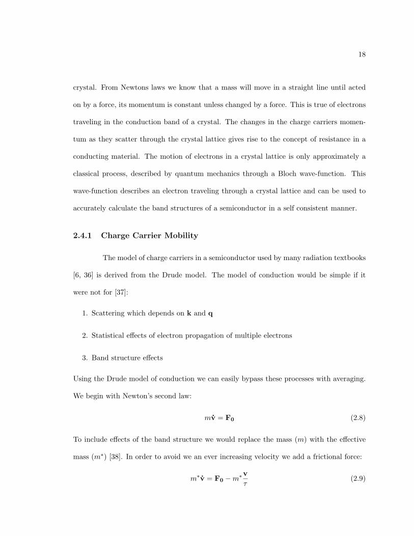
2.4.1 Charge Carrier Mobility
The model of charge carriers in a semiconductor used by many radiation textbooks
[6, 36] is derived from the Drude model. The model of conduction would be simple if it
were not for [37]:
1. Scattering which depends on k and q
2. Statistical effects of electron propagation of multiple electrons
3. Band structure effects
Using the Drude model of conduction we can easily bypass these processes with averaging.
We begin with Newton’s second law:
mv = F0 (2.8)
To include effects of the band structure we would replace the mass (m) with the effective
mass (m∗) [38]. In order to avoid we an ever increasing velocity we add a frictional force:
m∗v = F0 −m∗vτ
(2.9)

19
Letting F0 go to 0 we have a solution for the velocity v ∝ e−tτ with τ as the decay time
constant. In the presence of an electric field the force is F = qE giving:
m∗v = −eE−m∗vτ
(2.10)
combining this equation with the assumption of steady state we have:
m∗v = 0 = −eE−m∗vτ
(2.11)
Solving for the velocity we have:
m∗v = eEτ (2.12)
We know from Ohm’s law that the current density is defined as j = σE. From electrody-
namics [39] we have the current density is given by j = env. Plugging in v from above we
have:
j = env =e2τn
m∗E = σE (2.13)
where σ is the conductivity, σ = e2τnm∗ = enµ, and µ is the mobility. This model is good
for low field, low frequency conduction where the velocity is on average isotropic in the
semiconductor, such as exist in HPGe detectors.
The source of the frictional force is scattering through the crystal lattice. By far the
most important scattering process for low energy electrons affecting conductivity is lattice
vibrations (phonons) [37]. Phonons take energy away from the electrons and keep them
energetically close to the conduction band edge. There are other scattering mechanisms,
which are elastic but still influence the conduction substantially. Among these are scattering
by charge impurities, neutral impurities, and surfaces. Phonons traverse the crystal lattice
as well and scatter by impurities in the crystal lattice as well as different isotopes of which
the crystal is composed

20
In this model we have the velocity as a function of the electric field strength
v = µ|E| where the coefficient is given by µ = eτ/m∗. The electrons scattering through the
crystal lattice gives rise to an effective mass of the charge carriers. This lattice dependence
also introduces a directionality to the effective mass, thus an effective mass is a tensor
relative to the crystal lattice. This directionality, coupled with the electric field results in
a directional dependence of the velocity in the crystal lattice as well. This directionality in
the charge carrier velocity is called the anisotropic drift velocity.
2.4.2 Statistics of charge collection
To understand the statistics of electron-hole pair production, let us assume that
the energy deposited by the incident radiation goes into causing lattice excitations and
ionization. If εi and εx represent the average energies needed to produce ionization and
excitation respectively, then the total deposited energy can be written as
Edep = εini + εxnx (2.14)
where ni and nx represent the total number of ionization and excitations produced by the
radiation. If we now assume that these processes follow Poisson statistics, it would mean
that the variance in the number of ionization and excitations can be written as
σi =√ni (2.15)
σx =√nx (2.16)
These two variances are normally not equal because of differences in the thresholds for
excitation and ionization processes. However if we weight them with their corresponding

21
thresholds, they should be equal for a large number of collisions, i.e.,
εiσi = εxσx (2.17)
εi√ni = εx
√nx (2.18)
Combining this with equation 2.14 gives
σi =εxεi
[Edepεx− εiεxni
]1/2
(2.19)
Let us now denote the average energy needed to create an electron-hole pair by wi. Note
that this energy includes the contribution from all other non-ionizing processes as well. This
means that it can be obtained simply by dividing the total deposited energy by the number
of electron-hole pairs detected ns. Hence we can write
wi =Edepns
(2.20)
or
ns =Edepwi
(2.21)
If we have a perfect detection system that is able to count all the charge pairs generated,
then we can safely substitute ns for ni. In this case the above expression for σi, yields
σi =[εxεi
(wiεi− 1)Edepwi
]1/2
(2.22)
Using Edep/wi = ns, this can be written as
σi =√Fns (2.23)
where
F =εxεi
(wiεi− 1)
(2.24)
22
is called the Fano factor. It is interesting to note here that even though we assumed that the
individual processes of ionization and excitations were Poisson in nature, but the spread in
the output signal can be described by the Poisson process only if we multiply it by another
factor. The reason, of course, is that these processes are not uncorrelated as required by
a strictly Gaussian process. The Fano factor was first introduced to explain the anomaly
between the observed and expected variance in the signal [40]. The simple calculations we
performed above do not produce very accurate results and they were only meant to motivate
the Fano factor. For detailed calculations see van Roosbroeck, W and Alkhazov.
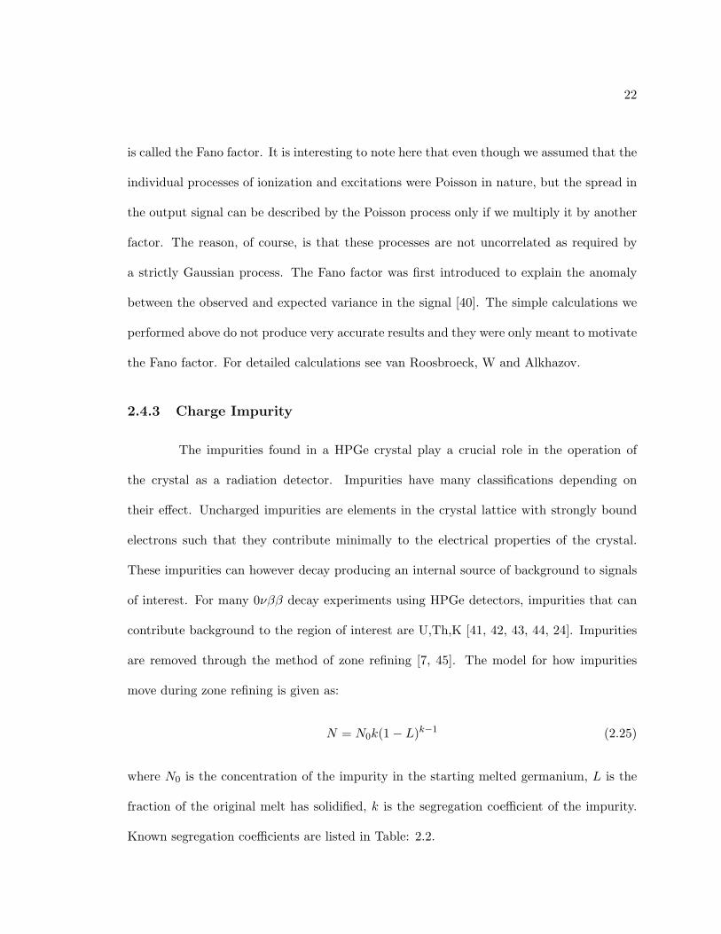
2.4.3 Charge Impurity
The impurities found in a HPGe crystal play a crucial role in the operation of
the crystal as a radiation detector. Impurities have many classifications depending on
their effect. Uncharged impurities are elements in the crystal lattice with strongly bound
electrons such that they contribute minimally to the electrical properties of the crystal.
These impurities can however decay producing an internal source of background to signals
of interest. For many 0νββ decay experiments using HPGe detectors, impurities that can
contribute background to the region of interest are U,Th,K [41, 42, 43, 44, 24]. Impurities
are removed through the method of zone refining [7, 45]. The model for how impurities
move during zone refining is given as:
N = N0k(1− L)k−1 (2.25)
where N0 is the concentration of the impurity in the starting melted germanium, L is the
fraction of the original melt has solidified, k is the segregation coefficient of the impurity.
Known segregation coefficients are listed in Table: 2.2.

23
Charged impurities are those elements which contribute significantly to the elec-
trical properties of an HPGe crystal. Of these type of impurities are donors and acceptors.
Donors have a loosely bound electron which it shares with the germanium crystal lattice.
Acceptors are the opposite of donors in that they want to loosely accept an electron from
the crystal lattice. Charged impurities play a crucial role in HPGe detectors. At the purity
levels germanium crystal are grown, manufactures must add charged impurities to make
a functional HPGe detector, these are referred to as dopant’s. The need for dopant’s is
illustrated in Fig. 2.4. The electric field without the dopant’s is very high at the inner
contact and very low at the outer contact, resulting in very poor charge collection. The
application of large voltages cannot compensate. By doping the high purity material with
the appropriate donors or acceptors, the initially neutral material must remove the donor
or acceptor charge leaving behind a net charge which extends the electric field through the
entire volume. Dopant’s enable high purity germanium detectors. Many common dopant’s
are used in HPGe detectors, many common in the semi-conductor industry are listed in
Table: 2.1. All High purity material
Table 2.1: Common shallow donors and acceptors that can be used in high purity germaniumsemiconductors [2].
Common dopant’s for use in GermaniumShallow Donors As P Sb Bi Li
Shallow Acceptors Al B Ga In Tl
After the material is zone refined and the proper dopant’s added, it is fabricated
into a large single crystal by the Czochralski method [45]. This method involves growing a
single crystal from melted material in a quartz crucible. The system is heated by a radio
frequency induction coil wrapped around the crucible in a process called RF heating. A

24
Figure 2.4: Comparison of the magnitude of the electric field for a coaxial HPGe detectorwith and without a charged impurities. The radius goes from an inner radius of 1.5 mmto an outer radius of 14 mm. The impurity density was given as constant at 0.0003 C/m3.The black line illustrate the electric field at depletion at 100 Volts up to 150 Volts appliedto the contact. The red line shows the electric field without charged impurities at 150 volts.

25
Table 2.2: Segregation coefficients for elements in germanium as reported by Trumbore[3].The elements U,Th and K are not known but of particular interest as sources of back-ground in HPGe detectors.
Elemental Segregation Coefficients in GermaniumElement Coefficient Element Coefficient
Co 1.00E-06 Sb 3.00E-03Zn 4.00E-04 Li 0.002Mn 1.00E-06 As 2.00E-02Fe 3.00E-05 P 8.00E-02Tl 4.00E-05 B 17Bi 4.50E-05 U -P 8.00E-02 Th -Pt 5.00E-06 K -Cd > 1E-05 Ag 4.00E-07V < 3E-07 In 0.001
Au 1.30E-05 Si 5.5Cu 1.50E-05 Pb 1.70E-04Al 7.30E-02 Bi 4.50E-05Ga 8.70E-02 Te 1.00E-06Sn 2.00E-02 Ni 3.00E-06
small dislocation free seed crystal is slowly pulled out of the melt as the material solidifies
into a single crystal. The seed is rotated as it is pulled to obtain a cylindrical ingot. To
prevent absorption of impurities the process takes places under argon gas [7].
2.5 Electronics
One of the key components in modern detector systems is the electronics readout
system. Many experiments and detector systems use many different electronics technologies,
however the all share the same basic principles for the electronic readout and optimization
of signal to noise ratio. Ultimately, the purpose of these pulse processing systems is to:
1. Acquire electrical signal from the detector.

26
Figure 2.5: Impurity profile of a germanium ingot [7]. The crystal growth seed is locatedat the 0 % end of the crystal.
2. Optimize the response of the system to:
• the minimum detectable signal
• energy measurement
• event rate
• timing
• insensitivity to variations in the pulse shape due to detector characteristics
3. Digitize and store the signal for subsequent analysis
Generally, these properties cannot be optimized simultaneously, so compromises
are necessary. In addition to these primary properties of the electronics readout system,
other considerations can be equally important like: resistance to radiation damage, low

27
power, portable, temperature, etc. . . . Many modern and accessible texts exists so the topic
of electronics will not be discussed any further here except when necessary.

28
Chapter 3
Charge Transport Simulation
3.1 Introduction
The Shockely-Ramo theorem is the basis for charge transport simulation in High
Purity Germanium (HPGe) detectors [46, 47, 48]. In this chapter we review this method and
present a computer code (CRT) to perform charge transport simulations in HPGe detector.
We discuss the most significant input parameters such as the geometry and impurity profile.
3.2 Charge Transport Code
Our charge transport code developed solves for the potential of a complex geomet-
rical germanium detector in three dimensions. The code was developed from scratch for
many reasons, including the high cost of commercial software to the scientific community
in general, and the lack of free software capable of solving for complex three dimensional
geometries in particular. Instead of patching several programs and data formats together
a complete solution provides seamless compatibility, as well as high level transparency. Fi-

29
nally, being general in the scope of the geometry but specific in the ultimate form of the
solution provides for efficient development, computational efficiency and design stability.
An accurate, verified model of the pulse shape formation process is needed. Such
an accurate simulation model has been developed (CRT), with experimental validation.
The model covers aspects necessary to completely describe the pulse formation process:
(1) Modeling of the electric fields, with and without space charge effects.
(2) Transport of the deposited charge, including second-order effects such as drift velocity
anisotropy from lattice orientation effects.
(3) Calculation of induced charge signals, using the weighting field formalism.
(4) Convolving with the electronic response of the analog readout system, e.g. a charge-
integrating preamplifier.
3.2.1 Field Solutions
CRT can solve for the fields given the applied voltages, the geometry and the
charged impurity profile. Solving for the electric field in a given region is most easily done
by first solving for the potential. Given boundary conditions, the relaxation method [39] is
a simple yet powerful method of solving the potential in the bounded region. However, it
proves difficult to solve the boundary conditions do not match up with the grid coordinate
system being used. HPGe detectors are often of very complex shapes and most often include
cylindrical and spherical regions.

30
Figure 3.1: A simple HPGe detector showing cylindrical, spherical and conic shaped regions.
Geometry
The geometry is described with Congruent Solid Geometry, where simple shapes
are operated on by a subtraction, intersection, or a union of one of more shapes to another.
A simple implementation of this method allows for the combination of simple shapes to ac-
curately represent a complex volume. The shapes are combined with the relevant material
properties. With the description of the geometry a Cartesian grid is built and superimposed
with a surface grid. The surface grid imposes the proper boundary conditions of the geom-
etry on the fields. Given a charge density profile, the code can then solve for the necessary
electric and weighting fields.
CRT constructs geometries using derived classes for each simple shape. Adding a
derived object that performs a Union, Intersection, or Subtraction function on two objects
we can make complex volumes from simple ones. We pass the constructed object to a
logical class providing material information about the object, like its permittivity or density.

31
Figure 3.2: Illustration of how congruent solid geometry descriptions can represent complexgeometries. Starting with a simple cylinder on the right, we can apply a subtraction ofanother smaller cylinder to produce a coaxial cylinder. We can then use a union to joinanother cylinder to the top to generate a semi coaxial detector shape.
Finally we pass the logical object to a physical volume class handling the actual placement of
the volume. The physical volume represents the object in question, defining its boundaries,
its position and any material properties. Any information needed, is passed through the
physical volume, and given the correct offsets to be passed to each constituent simple solid.
Grid
A graphic of a cylinder represented on a course Cartesian grid is shown in Fig. 3.3.
We can see the short comings inherent to this method. Even with very small grid spacing,
there will be significant error near the surface which can collectively increase the error of
the integral cells and final solution. Besides the inability to account for the volume and
total charge, the greatest error comes from not being able to correctly enforce the boundary
conditions of the electric field at the surface.

32
Figure 3.3: Illustration of how a cylinder super-imposed on a Cartesian grid. In red are thegrid points of a regular Cartesian grid. With the cylinder superimposed the blue shows thevolume of our effective solution.
CRT superimposes several grids. The basis is a Cartesian grid used to represent
the potential at any point in the volume. A second non-regular grid represents the surface
at any intersection of the surface with the Cartesian grid. This method faithfully reproduces
the correct boundary conditions at the surface, most notably that the electric field is normal
to the metallic surface [39].
CRT is written in the C++ language [49] making use of many of the key concepts.
Defining base classes, inheritance, along with the extensive use of pointers. Each regular
grid point contains the potential and charge at that point, as well as pointers to each of
the six nearest neighbors and the distance to each. The CRT code uses relaxation to solve
for the potential [39] and using pointers to get the nearest neighbor information relieves
the code of costly overhead with the use of a little extra memory. The consequent speedup
makes this simple relaxation implementation more than sufficient for calculating electric

33
Figure 3.4: This figure demonstrates the relationship between each grid point and the super-imposed surface grid point. The Blue connections are pointers from each grid point to itsneighbor. The Red connections are pointers to the surface grid point potential. These linkshave the correct distance to the correct nearest neighbor. These surface elements can beunderstood as the superposition of two different grid systems. These two grids allow us theease of a regular Cartesian grid while using the surface grid to correctly enforce boundaryconditions. The ability to build the surface grid in any non-uniform way allows for theconstruction of complex geometries.
fields within the scope of this problem. These nearest neighbor pointers of the regular grid
point to the necessary value at the surface for unambiguous calculation.
3.2.2 Charge Transport Dynamics
CRT can build directly or read from a file the weight potentials for each contact as
well as the electrical potential given a charge impurity profile and applied voltage. From this
CRT builds the electric field. For charge transport dynamics, a third order, 3D polynomial
interpolation of the potential is built and stored for each grid point. This allows for a
second order electric field such that the electric field and derivatives are smooth at any cell
boundary. For dynamics,the interaction locations and deposition energies are read in from
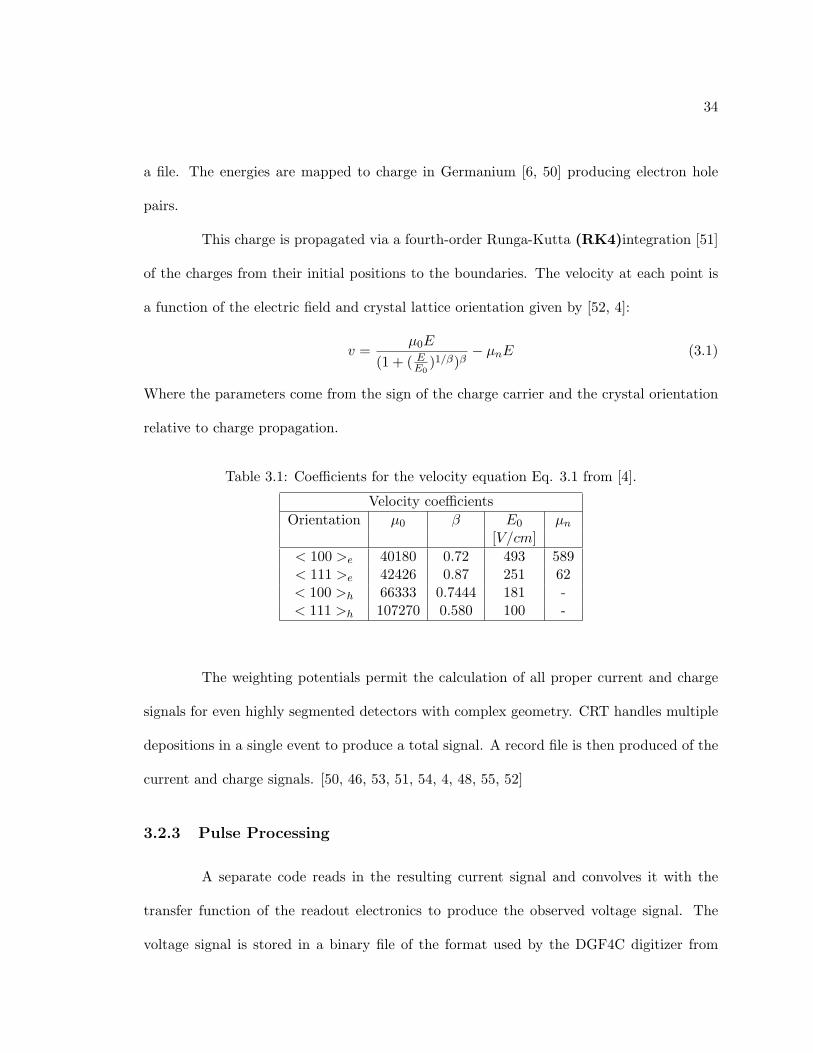
34
a file. The energies are mapped to charge in Germanium [6, 50] producing electron hole
pairs.
This charge is propagated via a fourth-order Runga-Kutta (RK4)integration [51]
of the charges from their initial positions to the boundaries. The velocity at each point is
a function of the electric field and crystal lattice orientation given by [52, 4]:
v =µ0E
(1 + ( EE0)1/β)β
− µnE (3.1)
Where the parameters come from the sign of the charge carrier and the crystal orientation
relative to charge propagation.
Table 3.1: Coefficients for the velocity equation Eq. 3.1 from [4].
Velocity coefficientsOrientation µ0 β E0 µn
[V/cm]< 100 >e 40180 0.72 493 589< 111 >e 42426 0.87 251 62< 100 >h 66333 0.7444 181 -< 111 >h 107270 0.580 100 -
The weighting potentials permit the calculation of all proper current and charge
signals for even highly segmented detectors with complex geometry. CRT handles multiple
depositions in a single event to produce a total signal. A record file is then produced of the
current and charge signals. [50, 46, 53, 51, 54, 4, 48, 55, 52]
3.2.3 Pulse Processing
A separate code reads in the resulting current signal and convolves it with the
transfer function of the readout electronics to produce the observed voltage signal. The
voltage signal is stored in a binary file of the format used by the DGF4C digitizer from
35
X-ray Instrumentation Associates. This allows us to run the same analysis code on both
the simulated and experimental signals for consistent comparison.
The transfer function captures the effect of a charge integrating preamplifier. The
functional form of the response can be read in from a file that has been produced from a
measurement or from a SPICE model [56]. The default behavior is to use a two parameter
analytical model to approximate the electronics response. This analytical model works very
well in general cases. Reading a response function in from a file allows one to fine tune
the simulation to an electronics design or existing electronics package [57]. The analytical
model is given as [58]:
R(t) =A
Td − Tr√π
2√
1.3
(exp(− t
Td)− exp(−1.3t2
T 2r
))
(3.2)
3.2.4 Verification and Validation
Validation of the electric field solution has been relatively straight forward. A
comparison for geometries with analytical solutions has been performed 3.5. The electric
fields are normal to the metallic surface in all cases tested. Explicit enforcement of this rule
is not necessary with the super-position of the surface grid.
The energy histogram in Fig. 3.6 sums up the three main systematic tests necessary
for this code. An input file was generated where an energy distribution was spread out
along a constant radius but varying angle. The model has crystal lattice anisotropic drift
velocity capabilities, however these results used an isotropic model where all charges moved
at the same speed given the magnitude of the electric field. This tested the ability of the
code to interpolate the electric field in 3D coordinates. The sensitivity of the current on

36
the weighting field made this very difficult. Thus the systematic tests we felt were most
significant for this code were:
• Charge conservation, charge is lost as a particle steps out of the volume, with such
high fields the velocities must have good integration method. We use RK4 integration,
charge is conserved in this model.
• Sufficiently smooth interpolation methods, the current is very sensitive to the weight-
ing field, so we must have a good interpolation method, otherwise the results are both
non-conservation of charge and inaccurate signals.
• Correctly account for non-Cartesian system in Cartesian coordinates. Interpolating
along an axis on a grid is fairly easy, interpolating in a 3D grid, is straight forward
as long as the point is sufficiently contained by Cartesian grid point. If we are near
a surface, most interpolation schemes introduce errors. Correct geometric accounting
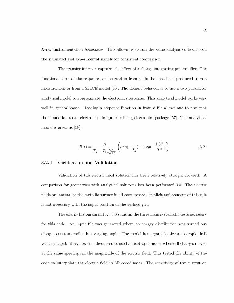
ensures that every path gives the correct pulse for the same energy for the same radius.
3.3 Charge Impurity Profile
The signal is a function of the velocity. The velocity and path depend on the
electric field in the detector. The electric field is a direct result of the boundary conditions
combined with the charged density of the charged impurities, both acceptors NA and donors
ND. The total charge density is the difference in these two impurities per unit volume.
The charge density is one of the most critical parameters in the computational
model. Ironically, the charge density, from the dopant’s, is the most difficult parameter
to measure and insufficiently understood. The underlying processes are understood, the

37
Figure 3.5: The potential of a true cylindrical coaxial HPGe from simulation compared tothe analytical solution [6].

38
Figure 3.6: Comparison between simulated energy depositions uniformly distributedthrough an HPGe detector and the energy given after charge transport simulation. Thistype of systematic test shows that the energy is preserved across the crystal volume. Thistype of test also shows that charge is conserved as well.

39
models exist, but few studies have been preformed to examine the nature of charge density
profiles in working high purity germanium detectors. A method to quickly obtain a charge
density profile is given in chapter 6.
The lack of these studies is a critical shortcoming in the current status of detector
characterization methods. A proper handle on the charged impurity profile is necessary for
any functional model of the detector response [7]. The impurity profile determines many
physical aspects of an HPGe detector performance, including the depletion voltage, the
capacitance, and the pulse shape characteristics directly. How to find the charged impurity
profile is given in chapter 6, along with a comparison to other methods.

40
Chapter 4
Single from Multiple Site Rejection
The signatures of events encountered in double beta decay experiments can be
classified according to the the spatial distribution of ionization in the semiconducting de-
tector. A detailed classification for these events is given in addition to the importance of
multiple site rejection and single site acceptance. A simple analytical model of the pulse
shape discrimination is presented as well.
4.1 Why we need it
The 0νbb-decay process has, in addition to the daughter nuclei, two electrons and
no neutrinos in the final state. The sum of the kinetic energies of the electrons is therefore
approximately equal to the Q-value for the decay. For the germanium isotope 76Ge this
energy release is Qββ = 2039 keV [59]. Electrons in the relevant energy range predominantly
deposit their energy in germanium via ionization. The range of the electrons is of the order
of millimeters [60]. Since the germanium detectors under consideration has a volume of the
order of 400cm3, the energy of the electrons will be fully contained within a small volume
of the crystal, if no hard bremsstrahlung is present. The signature of 0νbb-decay events is
thus a peak at the energy of 2039 keV.
41
Background events are produced from a wide variety of physical processes with
alpha’s, beta’s, gamma’s, pion’s, muon’s, neutrons, etc. . . , in this work we concentrate
on the dominant background contributions in underground low background germanium
experiments resulting from gamma radiation. Background rocesses not treated here are
considered more fully elsewhere [61] as is the overall neutron flux from radioactive elements
in the surrounding bed-rock.
All radioactive materials with Q-values larger than Qββ are potential background
sources for the 0νββ-decay process. A fraction of the released energy can be deposited
inside a detector, such that the measured energy is in the region of interest (ROI) the
Qββ-value. Photons in the MeV range predominantly deposit their energy via Compton
scattering. Their absorption length is of the order of centimeters. Considering the size of
the germanium crystals under study, process with photons in the final state are likely to
deposit only a fraction of the total energy inside one detector. The signature of the 0νββ
decay signal and the main background signatures are classified according to the particles in
the final state1.
• Single Site:
– Two electrons: This class encompasses the neutrino-less and neutrino accompa-
nied double beta decay processes. If the energy resolution is better than 10keV,
the two modes of double beta decay can be separated, since the energy region
around the Qββ-value is not populated by 2νββ-decay process. The two electrons
deposit their energy locally, i.e. on a millimeter scale, see Fig.4.1.1The Single Site versus Multiple Site categorization was adapted from Abt[62], indicating wether energy
deposition occurs entirely within a single detector region or if energy deposition is divided amoung severaldetector regions.

42
• Multiple Site:
– Photon(s) and electron: This class contains all β− decay processes accompanied
by the emission of one of more photons which occur inside the detector or close
to its surface. The energy of the electron is deposited locally, whereas the photon
scatter and not all of its energy is necessarily deposited inside the detector. An
example for this class is the decay of 60Co inside the germanium.
– Photon(s) and positron: Similar to above, this class contains all β+-decay pro-
cesses accompanied by the emission of one or more photons inside the detector.
The positron deposits most of its energy locally and annihilates. The photons
(the two 511 keV gammas plus any additional photons) scatter and mostly do
not deposit all of their energy inside one detector. The most prominent example
for this class is the decay of 68Ge inside the germanium.
– Photon(s) only : If the decay occurs outside the germanium detectors, α-particles
of electrons can be stopped before they reach the crystals. Most prominent
examples are the decays of 208Tl and 214Bi which come from radio-impurities in
the detector surrounding.
– α-particles: Surface contaminations with 210Pb or other isotopes which decay
via α-emission can contribute to the background. α-particles in the 2-10 MeV
range deposit their energy on a 2-50 µm scale. α-particles emitted at the surface
therefore potentially deposit only a fraction of their initial energy inside the
active volume of the crystal.

43
Figure 4.1: The electron range in HPGe versus initial energy. The solid horizontal lineshows the 1 mm electron path length close to 0.9 MeV.

44
4.2 Statistical Moments
In this section we discuss the use of a pulse shape discrimination method derived
from statistical moments but not normalized to a normal distribution. The properties of
this parameter space provide an excellent basis for a complete framework to describe pulse
properties.
In order to arrive at a distinct formulation of statistical problems, it is nec-essary to define the task which the statistician set himself: briefly and in itsmost concrete form, the object of statistical methods is the reduction of data.A quantity of data, which usually by its mere bulk is incapable of entering themind, is to be replaced by relatively few quantities which shall adequately rep-resent the whole, or which, in other words, shall contain as much as possible,ideally the whole, of the relevant information contained in the original data. [63]
4.2.1 Statistical Moments properties
In the statistical description of any distribution of data point we use the statistical
language of moments. When a set of values has a sufficiently strong central tendency, that
is, a tendency to cluster around some particular value, then it may be useful to characterize
the set by its moments. A moment in this sense derives its meaning from physics and is
given mathematically by the nth moment of a real-valued function f(x) of a real variable
about a value c is
µn =∫ ∞−∞
(x− c)nf(x)dx (4.1)
The real value c is the mean of the function at the origin. Given the subtle assumption that
all moments are about the origin leading to the subtlety c→ µ.
The zeroth moment (n = 0) gives the area under the curve.
µ0 =∫ ∞−∞
(x− c)0f(x)dx =∫ ∞−∞
f(x)dx (4.2)

45
In the context of signal filters, this moment is preserved for most filters including a moving
window average. Few filters guarantee the preservation of higher moments. For discrete
signals this takes the form:
µ0 = area =N−1∑j=0
xj (4.3)
The next moment for n = 1 is the mean of the function and is given by:
µ1 =∫ ∞−∞
(x− µ)1f(x)dx =∫ ∞−∞
(x− µ)f(x)dx (4.4)
where µ is the mean. This may be confusing to have the mean defined in terms of itself,
but this is because this gives us the translated mean about the origin. If we assume that
the mean is already at the origin, then c = 0 in what follows. For discrete signals we have
the form:
µ1 = mean =1N
N−1∑j=0
xj (4.5)
The second moment, n = 2, is the variance of the function given by:
µ2 =∫ ∞−∞
(x− µ)2f(x)dx (4.6)
For discrete signals we have the form:
µ2 = variance =1
N − 1
N−1∑j=0
(xj − x)2 (4.7)
We note that σ is defined as σ =√variance.
The third moment, n = 3, is the skewness of the distribution. The skewness of a
function is a measure of its lopsidedness. A symmetric distribution will have a skewness of
zero. The skewness is given in the usual way:
µ3 =∫ ∞−∞
(x− µ)3f(x)dx (4.8)

46
Again, for discrete signals this has the form:
µ3 = skewness =1N
N−1∑j=0
xj − xσ
3
(4.9)
A distribution that is skewed to the left has a negative skewness and one to the right has a
positive skewness.
The fourth moment, n = 4, is the Kurtosis of the distribution. The kurtosis
measures if a given distribution has a peak or a flat shape to it.
µ4 =∫ ∞−∞
(x− µ)4f(x)dx (4.10)
Again, for discrete signals this has the form:
µ4 = kurtosis =
1N
N−1∑j=0
xj − xσ
4− 3 (4.11)
We will note that the value 3 subtracted from the end make the value zero for a normal
distribution.
These moments are important to the application of filters to noisy data. Few filters
preserve moments higher than n = 0. One exception is the Savitsky-Golay filter (SG) [51].
This is a filter in the time-domain as opposed to the frequency domain. SG preserves up
to a designated nth moment. Each physical characteristic of a pulse is related to one of
these moments, and if we want to be able to discern signal from noise we must preserve the
necessary moment. SG can remove noise in a very simple way in the time domain while
retaining a designated nth moment of the information. Thus SG is very important to pulse
shape analysis applications.
Another important statistical quantity to the field of radiation detection is the
Fano factor. The Fano factor relies on moments one and two, n = 1 & n = 2. The Fano

47
factor is defined as the ratio of the variance to the mean:
F =σ2
µ(4.12)
This is a measure of the dispersion of a probability distribution. It was formulated to
explain integrated charge of a specific energy in radiation detectors had a spread due not
only to the electronic noise but also due to the detector material properties [40].

48
4.3 Pulse Shape Discrimination
4.3.1 Introduction
Pulse Shape Discrimination (PSD) is the process of extracting information from
each pulse produced by radiation interaction with a detector. Pulses often go through
several stages of amplification. As the signals travel through the detector and associated
electronics noise accumulates in the signal. This noise must be minimized in order to extract
the maximum amount of information from a pulse [50, 64].
Assuming reasonable minimal noise, there exists a great deal of information that
can be extracted from pulse shapes. Current off-the-shelf systems use the pulse to deter-
mine the energy deposited from an interaction. However, particle identification, geometric
information, and even particle paths can be extracted from these pulses [9, 57].
The PSD technique used to distinguish multi-site events from single-site events in
the IGEX experiment is based on 3 moments of the current pulse. Unlike the statistical
moments of the previous sections, these moments were designed to maximize the ability to
discriminate specific information from current pulses of characteristic shape [9]. The first
parameter is the pulse rise time, the second is the full width from the half width, the third
is a normalized moment about the center of mass.
4.3.2 Aalseth PSD Method
The discrimination technique explored here is the method developed by Aalseth
et.al.[9, 65], using three energy independent parameters to discriminate multiple site events
from single site events. This method takes a raw current pulse from a digitizer, and ap-
plies any of several Digital Signal Processing (DSP) techniques. The only necessary DSP

49
Figure 4.2: Theoretical PSD parameter space with color indicating the distance betweenmultiple interactions.
techniques is smoothing, which is done with the Savitsky-Golay filter [51]. This filter was
discussed previously.
The first parameter is the timing information. Given a voltage signal, the most
obvious timing is the rise time (τ) of the voltage pulse, often taken as the time it takes to
go between 10% and 90% of the maximum height of the voltage pulse. The 10% to 90% is
often called the constant fraction discriminator (CFD) and it used to truncate noise from
the measurement. Techniques to measure the rise time of a voltage pulse are given by the
IEEE [66].
The rise time can come from the CFD of the voltage pulse, however in this method
all of the parameters come form the current pulse. The current pulse, I(t), comes from
discrete differentiation of the voltage pulse. The rise from from the CFD applied to the

50
Figure 4.3: A current pulse with the 10% to 10% of the maximum enclosed in a box. Thetimming points needed are the start time, the end time and the time directly in the middleof these two, called the mid time.
current pulse begins at the 10% level to the left of the maximum and goes until it reaches
the 10% level to the right of the maximum. Fig. 4.3 shows a typical current pulse with a
box encompassing the timing information.
The second parameter used is the front back half back area (FHBH). If we start
at the center of the current rise time, and integrate the area before this we have the front
area. If the we integrate the area after this, we have the half back area. This is illustrated
in Fig. 4.4.
FrontHalf = B =∫ τ1/2
τi
I(t)dt (4.13)
BackHalf = C =∫ τf
τ1/2
I(t)dt (4.14)
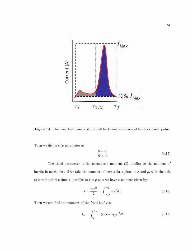
51
Figure 4.4: The front back area and the half back area as measured from a current pulse.
Then we define this parameter as:
B − CB + C
(4.15)
The third parameter is the normalized moment (I), similar to the moment of
inertia in mechanics. If we take the moment of inertia for a plane in x and y, with the axis
at x = 0 and rise time τ , parallel to the y-axis we have a moment given by:
I =mτ2
2=∫ τ/2
−τ/2mx2dx (4.16)
Then we can find the moment of the front half via:
IB =∫ τ1/2
τi
I(t)(t− τ1/2)2dt (4.17)

52
and the back half is given by:
IC =∫ τf
τ1/2
I(t)(τ1/2 − t)2dt (4.18)
Then the normalized moment is given by:
IN =IB − IC
I(4.19)
The first note about these parameters is that the interaction location is lost. This
is to say that these parameters are degenerate to the azimuthal angle and height of a
cylindrically symmetric detector, so we cannot extract from a current pulse. This, however,
is not a weakness because for experiments such as Majorana there is a much more important
piece of information that can be extracted. We can extract whether an event was single site
or multi site.
A single site event is exactly that, a photon interacts with an electron in a re-
stricted, contiguous region of space. If a photon is completely absorbed by an electron,
or in a detector a photon Compton scatters only once and then escapes the crystal, single
site events are produced. Ultimately, we are limited by the spatial resolution of our PSD
techniques, and cannot resolve events as single or multiple site if they occur too together.
Hence, a photon which Compton scatters several time in a very small volume of the detector
may be classified as single site by our PSD technique, even though, from a physics perspec-
tive events occur at several distinct regions. From a functional perspective any event which
can be identified as multiple site cannot be double beta decay [23], so ultimately, our spatial
resolution limits our ability to cut background events from a double beta decay experiment.
The Aalseth PSD method is excellent at discriminating if a current pulse was in fact
due to one ionization event or several within the time of the pulse duration. This technique

53
is often called a radial discriminator because it is assumed that two events, happening at
the same time at the same radius, will look like a single event because it will take them the
same mount of time to get to the collecting electrode. Thus, the current pulse will look like
a single event.
4.3.3 Analytical Model for PSD
We can write a simple model for a current pulse given an interaction radius if we
deal only with a coaxial detector. Second, if we assume that all charge carriers travel at
saturation velocity at all times. These assumptions are not very restrictive and produce a
surprisingly good model of the current pulse coming from the detector. We can write this
model as
I(r0, vc, t) = Q1
ln(Ri/Ro)vc
1r0 + vct
(4.20)
where r0 is the energy deposition radius, vc is the saturation velocity for a given charge
carrier, since the distinction of electron or hole can make a significant difference. Given
the constant velocity, we can easily solve for the time it takes to reach the corresponding
electrode with
τe =Ro − r0ve
(4.21)
τh =r0 −Rivh
(4.22)
A function can be used with a Heaviside step function to account for the finite path while
integrating over all time. However with careful consideration of individual integration limits,
the Heaviside step functions are not necessary.
The first parameter is simply the maximum of the two charge carrier collection
times, which is the rise time as it would be measured. If the electron transport time is

54
longer than that of the hole, we use it, or vice versa. For multiple site events, we simply
use the longest transport time. The longest transport time, for any event whether single or
multiple site, is τ .
The second parameter space is the front half back half (FHBH) area, given by
the integral of the front half and the back half of the current:
B =∫ τ/2
0I(r0, t)dt =
∫ τ/2
0(Ie(r0, t) + Ih(r0, t))dt (4.23)
So,
B =∫ τ/2
0(QDve−r0 + vet
+QDvhr0 + vht
)dt (4.24)
with D = 1/ln(Ri/Ro). It must be pointed out that the integration to τ/2 could be greater
than the transport time for that charge carrier τc/2. So care must be taken with this
integration limit.
We need the other side of this integral which is given as C:
C =∫ τ
τ/2(QDve−r0 + vet
+QDvhr0 + vht
)dt (4.25)
We have the FHBH parameter B − C given by the integral equation:
B − C =∫ τ/2
0(QDve−r0 + vet
+QDvhr0 + vht
)dt−∫ τ
τ/2(QDve−r0 + vet
+QDvhr0 + vht
)dt (4.26)
Thus, given τ we can easily integrate to find the FHBH parameter in this model.
4.3.4 Velocity and the PSD parameter space
The focus of this analytical parameter space model is to show that by including
anisotropic drift velocities in our models, we can improve our ability to get at the relevant
information in these experiments. If the Aalseth PSD method is to be improved on, then

55
Figure 4.5: The PSD line for single site events as the interaction point moves along theradius. The different lines indicate the effect of different combinations of drift velocities forelectrons and hole respectively.
there must be an affect on the PSD parameter that can be discerned. One parameter to
explore is the effects of different electron(ve) and hole (vh) drift velocities. Such an effect is
illustrated in Fig.4.5.
From Fig.4.5, we can see that velocity of the charge carrier not only affects the
signal site curve through PSD space, but the velocity of each charge carrier affects this
curve differently. This can be translated into the statement that the single site curve
through PSD space contains information about the velocity of the charge carriers. The
question that remains is the nature of noise in the PSD space and if the differences due to
velocity are significant enough to be extracted from this noise.

56
4.3.5 Notes on PSD
We had to discern if an anisotropic drift velocity will affect the PSD results. We
have established that it will. Next we must show significance in that some of this information
can be extrapolated out of the noise inherent in the signal. So we asked how the noise in
the current pulse affected the PSD data.
For the pulse time information, the current pulse is a set of discrete data points in
time. If there is jitter (error in the timing of the data point) it cannot be distinguished from
an error in the current pulse. This is due to the fact that the current is in fact a continuous
signal and displacement from noise in the time direction is the same as a displacement
current value. Error in the timing is the same as error in the current, so we will refer to a
single error and assume it is simply of the current.
For the discrete current data points any error will effect the pulse width parameter
space by inducing an expansion or contraction in the space. This effect is linear with the
error and to be expected. This is not magnified in any way, neither is different in part of the
space as it is from another. In fact this error is greatly reduced by using a Savitsky-Golay
filter [51].
The error introduced to the FHBH area parameter space is different from that of
the rise time. If we assume the error is additive to the current (as opposed to multiplicative)
we can use the toy model above to ascertain its effect in this parameter space.
B′−C ′ =∫ τ/2
0(I(t)+e(t))dt−
∫ τ
τ/2(I(t)+e(t))dt = B+EB−(C+EC) = (B−C)+(EB−EC)
(4.27)
57
The denominator gives us:
B′+C ′ =∫ τ/2
0(I(t)+e(t))dt+
∫ τ
τ/2(I(t)+e(t))dt = B+EB+(C+EC) = (B+C)+(EB+EC)
(4.28)
The resulting equation with error is:
B′ − C ′
B′ + C ′=
(B − C) + (EB − EC)B + C + EB + EC
(4.29)
Given that the error EC is approximately the same size as EB the contribution to the
numerator is very small, but the contribution to the denominator will push this parameter
toward the origin. Given that the error at any given point can be greater than or less than
the current at that point, but it cannot be negative due to the choice of baseline, given
that it is part of the pulse and well removed from negative values. The sum of the error
cannot be negative given the CFD level is much greater than the error as a requirement of
a good CFD [66], any error will push this parameter toward the origin. The range of this
parameter is both positive and negative due entirely to the numerator. Thus adding error
to the denominator will contract this parameter range toward the center.
The error contribution to the normalized moment is very different from the other
two parameters. If the error is once again additive, then it can be separated from the
current in the integral like so:
M ′ =∫ τ
0(t− τ
2)2(I(t) + e(t))dt =
∫ τ
0(t− τ
2)2I(t)dt+
∫ τ
0(t− τ
2)2e(t)dt = M + E (4.30)
while the denominator gives:(∫ τ
0(I(t) + e(t))dt
)τ2
12=τ2
12(B + C + E) (4.31)
Thus the error in the denominator will contribute in a linear fashion, meaning here uniform
everywhere in the PSD space. The numerator, however, multiplies the error by its distance

58
from the mid-point squared. This is a very non-linear contribution not only in time but
also in the parameter space. One conclusion is that error will have the greatest affect for
the longest pulses. Given the error term in the denominator is linear while that in the
numerator is multiplied by a square term, the error will push the normalized moment away
from the origin, and in a non-linear fashion. The error in the normalized moment maybe
by far the most significant in the PSD parameter space.
The ultimate result of errors introduced into this PSD method are a contraction
of data in each dimension. Error in the timing information is referred to as timing jitter
whose effects are nominal compared to the other two dimensions. The FHBH and Moment
dimensions contract with the introduction of error, or noise, to the signal. The effect is
linear, but given the discrete nature of the PSD algorithm a contraction of the space will
make discrimination more difficult. The acceptable levels of error for any signal of interest
can be evaluated with this simple analytical model. In order to asses the impact of this
method, however, we must introducea figure or merit capable of directly comparing alternate
methods.
4.4 Figure of Merit
A figure of merit,(FOM), is in general some quantity used to characterize the effi-
cacy of a method relative to alternative methods. The FOM commonly used in neutrinoless
double beta decay experiments, and used through out this work, is defined by Aalseth et.
al. [67] with the form
FOM =εββ√
εbackground(4.32)

59
where εββ and εbackground are the acceptance fractions of the discrimination for 0νββ decay
events and background events, respectively. The usefulness of this FOM definition is that
it is a multiplier to the standard half-life limit. This gives the direct improvement that one
might gain in half-life sensitivity of the experiment due to the method of discrimination.
Thus any analysis method can be compared by the FOM that it produces to any other
analysis method.
60
Chapter 5
A P-type Modified ElectrodeDetector: Overview of DetectorProperties
5.1 Introduction
An n-type germanium crystal with a small with a small point contact was reported
by Luke [68] in 1989. Barbeau et al. [8] recently presented, for the first time, the implemen-
tation of this geometry as a p-type point contact (PPC) detector. Having a 330 eV energy
threshold and energy resolution of 1.8 keV at 1332 keV, the performance of this detector
has generated interest in the nuclear science community working on ultra-low background
radiation measurements. At the time of the Barbeau et al. [8] paper , only one such
PPC detector had been extensively studied, thus the question arises regarding the future
availability and potential production rate of this detector design. This chapter presents an
overview of the influence of the impurity concentration1 and the impurity profile of the ger-
manium crystal on the performance of an operational PPC detector. We present the results1Throughout this paper the term “impurity concentration” is used as short hand for “net electrically-
active impurity concentration”. Similarly, the term “impurity profile” is short hand for “net electrically-active impurity concentration spatial profile”.

61
of field modeling and charge transport simulations of PPC detectors. We use consistency
with the depletion voltage, the charge transport time and the depletion capacitance curve
of the existing PPC detector to establish the reliability of our models. The results of our
simulations and comparison to known germanium ingot characteristics suggests that the
PPC design is a feasible detector for regular manufacture, not unlike typical p-type coaxial
detectors.
5.2 Motivation for the P-type Detector Geometry
There are two consequences to the electrode configuration of a PPC detector, as
shown on the right in Fig. 5.1[8]. The first consequence is a reduction of the detector
capacitance to ∼ 1 pF in comparison to ∼ 40 pF for a typical semi-coaxial detector [6].
The reduced capacitance permits a lower energy threshold [50], and an improved ability to
resolve spatially separated charge depositions through pulse shape analysis (PSA). Barbeau
et al. [8] have already reported one potential application of this detector design – the
measurement of neutrino-nucleus coherent scattering. Another important application, the
use of HPGe detectors in searches for neutrino-less double beta decay [23], provides a
stringent set of performance requirements. Those requirements include excellent energy
resolution (better than 0.2% FHWM at 2MeV), high mass detector elements(≥∼ 0.5 kg),
amenable to implementation in an ultra-low radioactive background environment and the
ability to distinguish events of interest from background events.
The predominant event identification method is based on neutrino-less double beta
decay producing a single-site energy deposition while gamma-ray backgrounds often produce
multiple site energy depositions [9]. Although several commercially available germanium

62
Figure 5.1: This notional diagram shows the comparison of an ordinary p-type detector(left) and a p-type point contact detector (right) showing a dead layer (dark), bulk p-typematerial (light), and an implanted contact on the central hole (thinned).
detector designs satisfy the energy resolution and mass requirements, there is typically
a trade off between event identification capability and the requirement to minimize the
introduction of radioactive contaminants in the electrical instrumentation and cabling com-
ponents needed for readout. Typical p-type coaxial HPGe detectors allow the greatest
control over radioactive backgrounds in detector construction materials; having only two
contact electrodes, there are a minimal number of readout components. However, the event
identification in typical p-type coaxial detectors is limited to PSA sensitive only to energy
depositions spatially separated in radial position [69]. An alternative is to use highly seg-
mented detectors which provide segment position, PSA-based radial position, and vertical
and phi-cylindrical coordinate through PSA of adjacent segments citation. The price paid
for this 3-dimensional event localization is the number and complexity of the read-out elec-
tronics (and their potential contaminants) required for the segmentation. In the absence of
a clearly superior choice of detector design, investigation into alternative designs, such as
the PPC detector, is warranted.
The central point-contact PSA for a PPC detector is substantially more powerful
63
in differentiating single vs. multiple site energy depositions than obtainable from standard
coaxial p-type detectors. This results from the stretching out of the charge collection
signal in time due to decreased weight fields and increased charge transport path lengths
relative to a standard p-type design. In contrast to segmented detectors, this improved
event discrimination ability does not increase the number or mass of cabling and local
electronics components, relative to the coaxial p-type. Likewise the PPC design does not
increase the complexity of the read-out instrumentation and subsequent analysis as will a
fully instrumented segmented detector [70, 71]. In the specific case of neutrino-less double
beta decay experiments, the PPC design profits from the thick (≈ 0.5 mm) dead layer
covering most of the crystal surface, which acts as a shield against external betas, x-rays,
and surface alpha particles. Hence the PPC detector design is compatible with good ultra-
low background design while improving upon the event discrimination capabilities of coaxial
p-type detectors.
For a successful future neutrino-less double beta decay or dark matter program, the
benefits of the PPC detector design may be desirable, but cost, difficulty in manufacturing,
and the rate of production are important considerations, especially in light of the number
of detector elements required for a future large-scale experiment. For these reasons it is
important this new detector design be straightforward and cost effective to manufacture. For
comparison, the cost of a generic p-type detector of 1 kg mass is approximately 1/3 the cost
per kg of a highly segmented n-type detector. If the cost and difficulty of manufacturing
a PPC detector is only incrementally higher than a common, p-type coaxial detector of
similar mass, broader applications are possible and essentially every detector manufacturer
will be able to produce them. The goal of this chapter is to investigate the likelihood of

64
Figure 5.2: Impurity profile of a germanium ingot [7]. The crystal growth seed is locatedat the 0 percent end of the crystal.
this outcome.
The driving factor for determining the type (p- or n-type) and the quality of
the detector is the distribution (amount and profile) of impurities throughout the ingot.
Fig. 2.5, reproduced here as Fig. 5.2, shows the typical impurity concentration and profile
of a germanium ingot. The impurity profile arises in the production of germanium crystals
due to the different segregation coefficients of the electrically-active trace impurities in the
Czochralski crystal pull method [7]. The analysis presented in this paper suggests that a
reasonably wide range of impurity profiles will lead to an acceptable p-type point contact
detector. To facilitate comparison, the same dimensions given in [8] for the first PPC
detector were used for this study (2.5 cm radius and 4.4 cm length).

65
5.3 Method
A study of the impact of the impurity profile on the acceptability of a PPC detec-
tor requires defining “acceptable performance”. The limits due to practical considerations
are: reasonable maximum applied depletion voltage and a maximum charge collection time.
These requirements together bound the usable parameter space of the model used for these
calculations. We use a model to pair impurity profile and the charge transport properties
of the detector to identify acceptable impurity profiles. Our impurity profiles can be some-
what arbitrary, therefore we use consistency with the measured depletion voltage, charge
transport time and the depletion capacitance curve of the existing PPC detector to establish
the reliability of our models. The calculation method uses a simulation of charge transport
through a germanium crystal in the presence of the appropriate electric field. Two such
codes have been developed at PNNL, an earlier 2-D model [57] and more recently a 3-D
version [72]. The earlier code was validated in the IGEX experiment [73] while the new 3-D
code has been shown to reproduce the 2-D solutions. The dynamics are handled with the
application of the Shockley-Ramo theorem2 [47, 46, 48, ?] and a parametric description of
charge carrier mobility [4].
In this study, the equation describing the impurity concentration of a crystal cut
from the p-type region of the ingot is given as a function of the crystal height alone [7].
The impurity density is given as:
ρ(z) = A+B
√z
H(5.1)
where A is the crystal’s minimum impurity concentration and B is the coefficient describing
the shape of the impurity profile. Both A and B have units of net electrically-active impurity2See Appendix A. for a derivation of the Shockely-Ramo theorem

66
concentration (i.e., atoms/cm3) with the radial dimension accounted for. The constant H is
the detector’s height. The independent parameter, z, is the distance between [0,H]. Using a
two parameter equation simplifies the description of the net charge impurity concentration
distribution, such that only the boundary values at either end ( ρ(z = 0) = A and ρ(z =
H) = A+B) are necessary. This is equivalent to the parameterization used for the detectors
of the GRETINA experiment [71] and is implicit in the discussions of Haller et al. [7]. As
the difference between the impurity concentrations at either end of the crystal decreases,
the profile becomes more linear. As the difference increases, the profile has more curvature
due to the square root dependence on z, as in Fig. 5.2.
Using the simulation, the voltage necessary for depletion is determined for the
(A,B) parameter space, this calculation is described in section 6.3. This parameter space
is bounded by a maximum allowable depletion voltage at 5 keV, consistent with typical
instrumentation, preamplifier high voltage filters, and achievable crystal surface dielectric
strength. The acceptable parameter space is compared with that for an equivalent p-type
coaxial detector in Fig. 5.4. In this context, an equivalent p-type coaxial detector has the
same external dimensions as the PPC detector, but with a central contact hole of depth
3.0 cm and radius 0.5 cm. Rather than comparing equal masses, this definition allows
comparison of the potential detectors that could be prepared from equally-sized crystal
blanks.
The time needed for full charge collection due to radiation interaction is determined
using the dynamics of charge carrier propagation in a semiconductor following Ramo and
Shockley [47, 46, 48]. Full charge collection time for the idealized PPC detector is generally
longer than an equivalent idealized p-type coaxial detector. As already stated, the charge

67
Figure 5.3: Simplified schematic of a typical HPGe preamplifier circuit focusing on thecontributions to the front end capacitance. The PPC preamp may or may not have aFeedback loop in the circuit.
collection time is a constraint on the acceptability of the detector. Low electric fields,
charge trapping, and ballistic deficit are important additional considerations with respect
to the PPC design. Relative to a typical coaxial p-type, the PPC detector design will have
larger regions of volume where the charge carrier velocity is below the saturation velocity
due to low electric field strength along the axis [74, 75, 68]. Furthermore, on average the
PPC design has longer path lengths for the charge carriers to reach collection electrodes.
These two features conspire to increase the probability of charge trapping resulting in poor
detector performance. However this possibility can be assessed using an IEEE measurement
standard [66].
At full operating bias voltage, a high purity germanium detector is in essence a
very large reverse biased pn-junction where the p (or n) region extends over the entire
volume of the crystal. As the voltage on one contact is increased the width of the depleted
region extends further into the crystal volume until it extends all the way to other electrode.
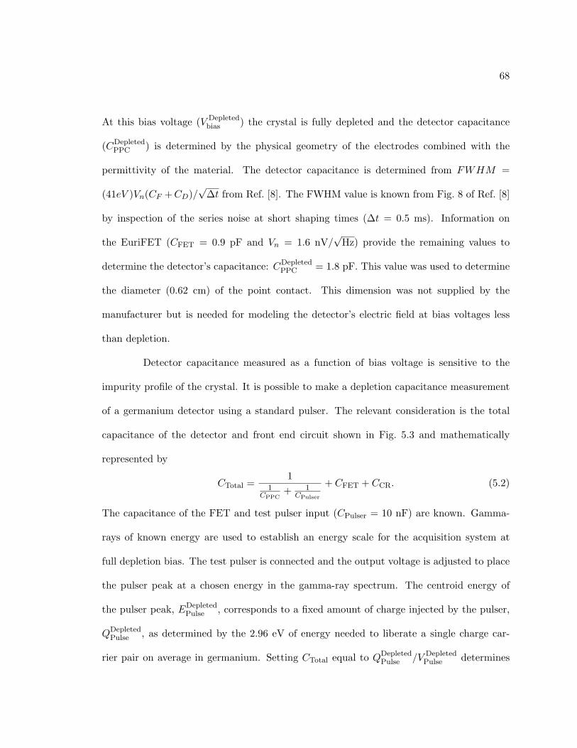
68
At this bias voltage (V Depletedbias ) the crystal is fully depleted and the detector capacitance
(CDepletedPPC ) is determined by the physical geometry of the electrodes combined with the
permittivity of the material. The detector capacitance is determined from FWHM =
(41eV )Vn(CF +CD)/√
∆t from Ref. [8]. The FWHM value is known from Fig. 8 of Ref. [8]
by inspection of the series noise at short shaping times (∆t = 0.5 ms). Information on
the EuriFET (CFET = 0.9 pF and Vn = 1.6 nV/√
Hz) provide the remaining values to
determine the detector’s capacitance: CDepletedPPC = 1.8 pF. This value was used to determine
the diameter (0.62 cm) of the point contact. This dimension was not supplied by the
manufacturer but is needed for modeling the detector’s electric field at bias voltages less
than depletion.
Detector capacitance measured as a function of bias voltage is sensitive to the
impurity profile of the crystal. It is possible to make a depletion capacitance measurement
of a germanium detector using a standard pulser. The relevant consideration is the total
capacitance of the detector and front end circuit shown in Fig. 5.3 and mathematically
represented by
CTotal =1
1CPPC
+ 1CPulser
+ CFET + CCR. (5.2)
The capacitance of the FET and test pulser input (CPulser = 10 nF) are known. Gamma-
rays of known energy are used to establish an energy scale for the acquisition system at
full depletion bias. The test pulser is connected and the output voltage is adjusted to place
the pulser peak at a chosen energy in the gamma-ray spectrum. The centroid energy of
the pulser peak, EDepletedPulse , corresponds to a fixed amount of charge injected by the pulser,
QDepletedPulse , as determined by the 2.96 eV of energy needed to liberate a single charge car-
rier pair on average in germanium. Setting CTotal equal to QDepletedPulse /V Depleted
Pulse determines

69
V DepletedPulse , the voltage seen at the FET gate induced by the pulser. When the bias voltage is
less than the depletion voltage the test pulser voltage remains fixed. However, the capaci-
tance of the detector has changed and becomes a function of the bias voltage, CPPC(VBias).
The changed detector capacitance results in a changed amount of charge injected at the
FET gate. This effect is measured as a displacement of the location of the pulse peak in the
gamma-ray spectrum. From the gamma-ray spectrum’s energy scale, the amount of charge
represented by the location of the pulser peak is determined as a function of bias voltage,
QPulse(VBias). Setting QPulse(VBias)/VDepletedPulse equal to CTotal gives the detector capacitance
as a function of bias voltage, CPPC(VBias). A measurement of the prototype PPC detector
was conducted in the manner described above.
5.4 Results
A successful impurity profile for a common p-type coaxial detector has the greatest
impurity concentration at the closed end of the detector, decreasing toward the open end. If
a point contact is simply substituted for a common p-type coaxial detector, the simulation
predicts a local minimum in the potential above the central contact. This local minimum is
difficult if not impossible to to remove except with the most extreme voltages applied. The
solution is to reverse the direction of the impurity gradient. This is essentially a flipped
orientation relative to the common p-type coaxial design.
The depletion voltage for the PPC detector as a function of the parameter space
is given in Fig. 5.4. The figure shows the depletion voltage as a shaded surface in the
2-D parameter space The lightest part, the lower edge, represents the maximum reasonable
depletion voltage of 5000 V. The darkest part, the upper left corner, represents the lowest

70
Figure 5.4: Calculated depletion voltage for given values of minimum charge impurity andcharge impurity profile. Dark to light shading represents low to high depletion voltagerespectively. The computation was cutoff at 5000 V. The darkest shading represents 0 V.Imposing a lower bound of 1000 V would only remove a small region very close to the origin.

71
depletion voltage. A cutoff for a lowest depletion voltage is not included in this graph. Note
that low depletion voltages imply long collection times, which is undesirable and discussed
further below. There are other practical limitations imposed by the crystal growth; intrinsic
germanium radiation detectors are rarely reported to have impurity concentrations less than
0.1 × 1010 cm−3 or greater than 5 × 1010 cm−3. These rough bounds set the reasonable
range of the impurity. The wide range of impurity profiles producing acceptable detectors
in terms of attainable depletion voltage as shown in Fig. 5.4. The typical coaxial p-type
detector design has a larger acceptable range of A and B values (shown by the dashed line),
yet given equivalent external crystal dimensions the two are not significantly different.
The charge collection time as a function of the A and B parameter space is given
in Fig. 5.5. The figure shows the maximum charge collection time as a function of the
parameter space. The charge collection time has a range from 250 to 2000 ns. Very long
collection times such as 2000 ns would lead to poor detector performance. PPC detectors
will generally have longer charge collection times in comparison to common p-type coaxial
detectors of the same external crystal dimensions.
Investigating the capacitance of these detectors, the prototype PPC detector [8]
capacitance (CPPC) was measured as a function of bias voltage. Fig. 5.6 compares this
measurement to simulation using the same dimensions and the two parameter model in
equation 5.1. A suggested relation of B = A [76], which is consistent with those impurity
concentration values reported in [68], is needed for a solution of the depleted detector capac-
itance using the measured detector depletion voltage, 2500 V. The simulation reproduces
the charge collection time of 700 ns as seen in the bottom of Fig. 11 in Ref. [8].
Note that the two capacitance curves do not match up at voltages below the

72
Figure 5.5: Calculated charge collection time surface parameterized by A and B. Theprototype PPC showed a charge collection of up to 700 ns.

73
Figure 5.6: Capacitance versus bias voltage for the prototype PPC [8] compared withsimulation.
full depletion voltage. This likely demonstrates demonstrates the need to add a radial
component to the model of the impurity concentration, equation 5.1. This hypothesis is
based on the results from an impurity concentration model having an ad hoc exponential
dependence on the radius. The degree of freedom provided by the radial dependence allows
different capacitance values at voltages less than full depletion. We explore the details of
the depletion capacitance and it measurement in chapter 6.
5.5 Conclusion
This work explores the relationship between germanium crystal impurity concen-
trations and the performance of detectors having the PPC design. Using a field simulation
for high purity germanium crystals, the range of charge impurity concentrations and pro-

74
files that will produce acceptable detectors is predicted. Detector acceptability is defined
by explicit calculation of depletion voltages and charge collection times. These measures
are used to compare with the first operational PPC detector [8].
This work shows that with current manufacturing methods, production of the
PPC detector design is confined to a range of impurity concentrations and profiles only
slightly smaller than a typical p-type coaxial germanium detector. Thus it is concluded
PPC detectors have the potential to become a moderately priced and universally available
resource for future applications.
Finally, this work suggests greater attention must be given to the radial impurity
concentration profile for complete understanding of the charge collection properties of the
PPC detector design. This subject is explored in chapter 6.

75
Chapter 6
Determination of the ImpurityProfile for a PPC Detector
6.1 Introduction
In the previous chapter we have shown that a PPC type detector may be made
from a wide range of impurity profiles. In this chapter we seek to demonstrate how to
measure the profile of a PPC detector. A method for using the measured capacitance
versus the applied voltage combined with appropriate simulations to model the impurity
profile is developed. A similar method for using an efficiency versus applied voltage, as
well as the commonly used four point resistance method is explained and contrasted to the
capacitance method developed.
Experimental characterization of an impurity profile for a detector can be resource
intensive and time consuming. Advanced PSA often uses a library of pulse shapes. To
statistically characterize the pulse shapes based on interaction position can take months.
However, the only alternative is simulation of the pulses as a function of position. If
simulations are to be used to build a library of pulse shapes, then a very good model for
the charge impurity density must be obtained. We demonstrate a method of solving for

76
the charge impurity density as a function of height and radius with a simple capacitance
measurement. This measurement gives the solution for a three parameter 2 dimensional
charge impurity density model. This can be used to simulate the electrical properties and
response of a solid state radiation detector.
There are only three ways to find the charge impurity model, one is an efficiency
scan and subsequent fit, another is a resistance measurement done at the manufacturer, the
third is a capacitance measurement and a subsequent fit. A scan to statistically characterize
the pulse shapes based on interaction position can only be used to build a pulse shape library,
and without a good model for the charged impurity profile. However, no modeling work can
be done to optimize any of the parameters for a particular experiment or physical process
signature without a charged impurity profile.
Pulse shape analysis (PSA) can be distinguished into two categories: parametric
and library. Parametric PSA uses specific parameters of the pulses to establish whether a
given pulse satisfies a given set of criteria. Common parameters include energy and charge
collection time. Library PSA builds a library of basis pulse shapes from which any pulse
can be reconstructed. Each experimental pulse is then compared to the library of pulses to
find a best match or a set of best possible matches. This corresponds to the position of the
interaction [77, 6, 78].
There are two approaches to making a library of pulse shapes. One can experi-
mentally scan a detector with highly collimated sources to produce a statistical pulse shape
for a set of interaction positions [31]. This can take months to complete for a single crystal.
The alternative is a parametric approach that uses computational modeling techniques to
build the pulse shape library. The computational method is very fast, yet its effectiveness

77
depends on the level of validation with experimental observables that can be achieved.
We present a method of doing a simple capacitance versus voltage measurement
to solve for the 2 dimensional charge impurity density equation with the third dimension
being symmetric. Given boundary conditions on the radius and height a 2 dimensional
solution guarantees a unique solution for this set of 2 dimensional boundary conditions.
Given this insight, the question becomes one of how sensitive are these measurements to
computational solutions and local deviations.
6.2 Physics of HPGe Detector Capacitance
For a depleted detector, the capacitance is completely determined by the geometry
of the conductors and the dielectric constant of the materials. Therefore the capacitance of
a true coaxial detector is given by the capacitance of two cylinders [6, 36]. If the crystal is
not depleted, then the capacitance takes a very different form.
In many modern text books on materials and their electrical properties we will
find the capacitance that relates the charge on a conducting surface to the voltage applied
for a p-n junction is termed the depletion capacitance [45]. The capacitance for reverse
biased p-n junctions is defined this way and using the energy stored in the electric field can
give very different and incorrect results.
A p-n junction has two basic types of capacitance. The first type is the differen-
tial storage capacitance or diffusion capacitance which arises from a rearrangement of the
minority carrier distribution due to diffusion into the bulk semiconductor as the voltage is
changed [79]. Differential storage capacitance is dominant under forward bias conditions.
The second type of junction capacitance is the transition capacitance or depletion-layer

78
capacitance. It is due to the variation of space charge with voltage in the depletion region
and is dominant under reverse bias conditions [45].
A transition capacitance is the result of the flow of majority carriers that changes
the widths of the total n and p space charge regions in response to a change in the applied
reverse bias potential V . A capacitance calculated from the total energy of the electric field
will give an incorrect result because it cannot account for energy lost to the lattice due to
scattering of the charge carriers as the boundary changes.
The variation of the space charge with an applied bias is due to the movement
of majority carriers in and out of the depletion zones. This is a very fast process that
takes on the order of picoseconds. Time constants associated with these charge variations
can therefore be neglected, and the associated capacitances can be considered frequency
independent [45].
Using the definition of the transition capacitance
Ct =∣∣∣∣dQdV
∣∣∣∣ (6.1)
as we increase the voltage, the depletion region of the junction changes. The dopant or
acceptor is neutral until this voltage sweeps away the neutralizing charge creating a space
charge. HPGe detectors are neutral except for the very thin natural p-n junction. As the
reverse bias inducing applied voltage to an electrode increases this p-n junction grows toward
the opposing electrode. This wide p-n junction region forms an active detector region. As
this active detector region grows charges from the dopant’s are swept away leaving a net
charge in the region as in Fig. 6.1. This net charge induces its own electric field which
adds by the principle of linear super position to the electric field due to the applied voltage
as illustrated in Fig. 2.4. In a p-type material the resulting space charge in the active
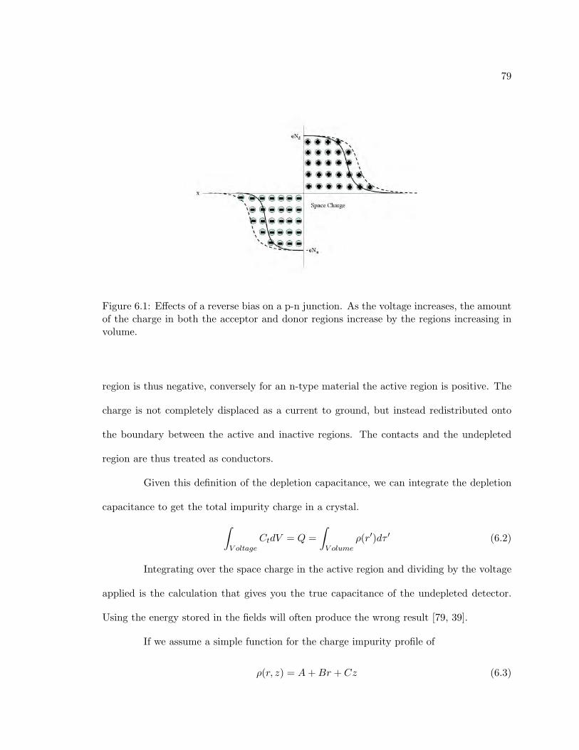
79
Figure 6.1: Effects of a reverse bias on a p-n junction. As the voltage increases, the amountof the charge in both the acceptor and donor regions increase by the regions increasing involume.
region is thus negative, conversely for an n-type material the active region is positive. The
charge is not completely displaced as a current to ground, but instead redistributed onto
the boundary between the active and inactive regions. The contacts and the undepleted
region are thus treated as conductors.
Given this definition of the depletion capacitance, we can integrate the depletion
capacitance to get the total impurity charge in a crystal.∫V oltage
CtdV = Q =∫V olume
ρ(r′)dτ ′ (6.2)
Integrating over the space charge in the active region and dividing by the voltage
applied is the calculation that gives you the true capacitance of the undepleted detector.
Using the energy stored in the fields will often produce the wrong result [79, 39].
If we assume a simple function for the charge impurity profile of
ρ(r, z) = A+Br + Cz (6.3)

80
We can then use the definition of the capacitance to pin down one of the parameters. The
most obvious parameter being the constant term A. The integration limits are therefore the
radius R and the height H of the detector. Integrating over the experimentally obtained
capacitance as a function of voltage, up to the depletion voltage, we have a value for the
charge Q. Then
∫C(V )dV = Q =
∫ρ(r, z)dτ = 2π
∫ H
0
∫ R
0(A+Br + Cz)rdrdz (6.4)
giving a parameterized limit to the three parameters A,B,C. Using this integrated charge
as a limit will greatly decrease the size of the parameter space that must be modelled.
6.2.1 Electronic noise and capacitance
The capacitance of an HPGe detector is not of secondary consideration. The
capacitance of the system including the HPGe detector influences strongly the electronic
noise of the system. The noise level of an HPGe detector is conveniently given as the
equivalent noise charge Qn. The equivalent noise charge is amount of deposited charge that
gives a signal to noise ratio of one [66]. For and HPGe detector the equivalent noise charge
is:
Q2n = i2nFiTS + e2nFv
C2
TS+ FvfAfC
2 (6.5)
where C is the sum of all of the capacitances shunting the input. The constants Fi,Fv and
Fvf come from the shape of the pulse, TS is a characteristic time of the circuit [58]. We can
see that the electronics noise contributions are related to the capacitance.
In Pulse Shape Analysis (PSA) methods the slope of the pulse to the noise must be
optimized in addition to the signal to noise ration alone. The jitter of the timing distribution

81
is:
σt ≈trS/N
(6.6)
where tr is the rise time of the amplifier. To increase dS/dt without excessive noise the
amplifier bandwidth should match the rise time of the voltage pulse. Often the rise time of
the voltage pulse is given as the 10% to 90% CFD rise time of the pulse [66]. The rise time
of the amplifier is given as:
tr =0.35fu
(6.7)
with fu being the amplifier bandwidth in Hertz. When amplifiers are chained together the
individual rise times add in quadrature as:
tr ≈√t2r1 + t2r2 + . . . (6.8)
Thus for good PSA, improving the signal to noise ratio will improve the time resolution so
minimizing the total capacitance at the input is very important.
6.3 Capacitance Measurement
The capacitance of an undepleted crystal can be measured at any applied voltage
by injecting a small voltage pulse into the crystal. Most HPGe detectors are made such that
the test pulse input bypasses the detector. In some detectors, like the PPC, the test pulse
input connects to the high voltage line allowing the pulse to travel through the crystal. A
simplified circuit diagram is given in Fig. 5.3. If the test pulse input bypasses the detector,
a line can be placed is such proximity to capacitively couple to the high voltage line and
inject test pulses through the crystal.

82
The voltages pulses were 20 mV square waves with a 20 ms duration. The 20
mV test pulse, ∆V is on top of the constant applied voltage V . At each applied voltage,
the detector system was run in multi-channel analyzer, (MCA), mode recording the ADC
values of the test pulses as if they were radiation events. The test pulses will produce
a Gaussian peak in the histogram whose peak position and FWHM is recorded for that
applied voltage. This procedure is repeated for each applied voltage of interest. The test
pulse peak will stop changing once the applied voltage is above the depletion voltage. The
results of this procedure on the PNNL PPC detector are recorded in Fig. 6.2.
A radiation source of know energy is used to calibrate the energy histogram. The
calibration will give the gain of the system
G =Epeak(eV )ADCpeak
(6.9)
Using this gain on the test pulse peaks Pi, for each voltage i, we have the number of electrons
produced
Ne =Pi ·G
2.96(eV/e−)(6.10)
, where 2.96 eV per electron is the energy per electron hole pair in germanium [6]. The
number of electrons can then be easily converted into Coulombs of charge produced in the
detector for use in the capacitance at each applied voltage.
C(Vi) =(1.602×10⁻¹⁹C)Pi·G
2.96(eV/e−)
20(mV )(6.11)
The capacitance as a function of applied voltage is now correctly in units of farads as show
in Fig. 6.3.

83
Figure 6.2: Capacitance measurement of a HPGe detector using injected voltage pulse,compared to 60Co 1332 keV peak.
6.4 Impurity profile from Capacitance
The model for the charged impurity profile is a three parameter 2 dimensional
equation given by:
ρ(r, z) = A+Br + Cz (6.12)
where A,B and C are simply the parameter space with the appropriate units. The parameter
set is exceedingly large and until we calculate the capacitances we do not know how close
we are to a good model. Calculating the capacitances is a very CPU intensive process, thus
we must use a small subset of the A,B,C parameter set. The necessary limit is given
by integrating the capacitance as a function of voltage, giving the total charge Q of the
detector.
Q =∫C(V )dV =
∫V olume
ρ(r, z)dτ (6.13)

84
The model for ρ(r, z) given above is easily integrated given the radius and height. The
measured capacitance as a function of voltage does have an associated error as well as lower
limit of 300 Volts. To account for this unknown region of the capacitance we set a 10%
upper and lower bound on the integrated charge. Thus we generate a parameter space file
for all A,B,C sets whose integrated value is in the range Q ± 10%. The range needs
to wide enough to account for the unknown region of the capacitance measurement while
being small enough to allow the problem to be tractable. The parameter space should allow
for negative values of parameters B and C.
A model of the charged impurity density will allows simulation of the capacitance
at any voltage below depletion. The capacitance is simulated using the CRT code. CRT
calculates the capacitance very simply, by first calculating the potentials at the applied
voltage V . The total charge in the active region is integrated as Q1. Then a ∆V of 20 mV
is added to the applied voltage and the potential is calculated. The total charge is again
calculated in the new active region as Q2. Thus the capacitance is simply:
C(V ) =Q2 −Q1
∆V(6.14)
CRT reads in each parameter set A,B,C giving the charged impurity density
ρ(r, z). CRT then calculates the capacitance at each voltage given in the measured ca-
pacitance curve. The χ2 is then calculated using the resulting capacitance curve and the
measured capacitance curve. This process is repeated for each parameter set until χ2 is
less than 1. Associating the χ2 with each parameter set in the parameter space shows a
very non-linear solutions set. The fitted parameter coordinates are surprisingly sensitive to
the parameter space. Thus minimization methods do not become effective until they are
sufficiently close to the solution coordinates. Several minimization routines were used, but

85
Figure 6.3: Iterating over a parameter space of the charge impurity profile, a fit to thecapacitance was found.
none proved more efficient than straight forward iteration until a solution was found. This
calculation will remain CPU intensive until an effective minimization routine is found.
6.5 Efficiency Method for Impurity Profile
In this method a count of the events in a given peak at each voltage with a
collimated γ source at several positions along the height of the crystal. The number of
counts in the peak, for each height for each voltage is proportional to the amount of volume
exposed to the γ rays. Taking many such measurements with a good knowledge of the total
volume should allow one to solve for the area of each height at a given voltage. This in turn
could produce a charge impurity profile as well as active volume versus voltage.
A 60Co source was placed between two lead slabs and aligned such that the col-
limated source irradiated a thin slice if the detector perpendicular to its axis. At a given

86
voltage, below depletion, only the active area will respond. The energy histograms were
recorded for 30 seconds with the collimated source at each of four heights from the base for
each voltage. The number of counts in a peak for some height at some voltage should relate
to the relative active area of the detector at that voltage. The measurement was made at
the University of Chicago and the results are given in Fig. 6.4.
The computational approach is much the same as with the capacitance approach.
CRT reads in the parameter set for the charged impurity model, and solves for the potential
at the given voltage. CRT then records the active region due to the calculated potential.
CRT then reads in a Monte Carlo of the detector with the appropriate collimated source,
recording the energies in a histogram of all events depositing energy in the active region.
The energy peaks are then compared to the measured energy peaks. The errors were to
significant to differentiate between a wide range of parameter sets.
There are many other drawbacks to this method. A fairly hot source needs to be
used to achieve a high signal to background as well as to be able to perform the measure-
ments in reasonable time. The γ rays scatter such that the radiation field volumes overlap
leading to spatial errors. As the voltage decreases below the depletion voltage the error, due
to very poor charge collection, increases well beyond any usable form. Thus the changing
nature of the charge collection as a function of voltage adds a great deal of uncertainty to
this method. Ultimately this method was determined to be inadequate due to the statistical
errors inherent to the measurement and the insensitivity of the computational solution set.

87
Figure 6.4: The Number of counts for a collimated 60Co source placed at four differentheights versus the applied bias voltage of the University of Chicago PPC detector. As theapplied voltage increases, the active volume increases thus the number of counts shouldincrease proportionately.
6.6 Four point Resistance Measurement
This method is common for manufactures to use on an HPGe crystal. The benefit
to manufactures is that it must be performed on an HPGe crystal before any surface treat-
ments, thus it can act as a quality control where the crystal can be rejected before expensive
treatments if the resistance is not in a specific range for a functioning HPGe detector.
This method measures the resistance which is related to the charged impurities.
The drawbacks of this method are that it measures the resistance very close to the surface,
it is only performed when necessary, it supplies only a couple of points, it can be off by as
much as 30%. The method can only be performed by the manufacture and gives insufficient
information with which to base simulations.

88
The resistivity of a semiconductor is defined as:
R =1
nq(µe + µh)(6.15)
where n is the free electron and hole concentrations, and µe and µe are the electron and
hole mobilities[80]. This resistivity can be measured in many ways, but sharing some very
common traits. The most common from semi-conductor manufactures is the four point
probe[80]. The four probes are generally arranges in-line with equal spacing between them.
Two probes carry the current while the other two probes measure the voltage derived from
the simple relationship:
V =RI
2πr(6.16)
Assuming equal spacing (s) between the probes, the total resistant can be given
as
R = 2πsF (V
I) (6.17)
where the most common spacings are 0.635 mm and 1.588 mm [80]. F is the correction
factors necessary to account for the edge effects, thickness effects, probe placement effects
and several other independent correction factors. The correction factors needed are much
more complex than the simple equation for the resistance. Common sources of error in-
clude sample size, minority carrier injection, probe spacing, current effects and temperature
effects.
According to Schroder:
Conventional four-point probe measurements give an average resistivity. Thisis suitable for uniformly doped substrates but is not sufficient for non-uniformlydoped samples in which the resistivity profiles need to be determined. [80].
The charge carrier dopant concentration (majority carrier) is related to the resis-
tivity, but it is not usually derived from it. Resistivity measurements are often preformed

89
by HPGe detector manufactures. given that the current flows at only very shallow depths it
will not give detailed information about a detector. Assuming a well behaved impurity con-
centration, measurements typically measure the resistance at four points, two at either end
of crystal center and two at either end of the outer radius. Giving a linear profile. These
measurements differ from the absolute impurity concentration by as much as 30 percent
[9, 81], however maintain good relative information.
The path of the current typically will have a small diffusion width and direct
path between the source and drain of the current. Only with extensive and complex sets
of measurements could the bulk of the material be sampled. Even if this were feasible
for HPGe detectors, the effort required would dissuade any manufacture from attempting
it. Manufactures apply a passivation and metalized surface to HPGe crystals, resistance
measurements must be made on bare crystal, thus a resistance measurement can only be
done by the manufacture.
6.7 Pulse Shape Library from a Scan
A library of pulse shapes can be made for an HPGe detector. The general method
involves two setup in a Compton scattering technique. A collimated source is incident on
the detector of interest, while a second detector is placed relative to the detector of interest
to maximize a Compton scatter. This second detector will also be collimated to the fist
detector and shielded from the source. A data set is collected with these two detectors in
coincidence and analyzed for a specific combined energy. With large statistics, this method
will produce a dataset of dominated by energy depositions from the intersection of the
source and second detector collimation paths in the detector of interest. A scan is very

90
resource intensive, as well it takes a very long time to complete, on the order of months per
detector.
6.8 Conclusion
We have reviewed the physics of capacitance in an HPGe detector. We have
written code that can correctly give the capacitance for an undepleted HPGe detector, given
a charged impurity density. The dependence of the capacitance on the charged impurity
profile for an undepleted HPGe detector allows an iterative search for the best charged
impurity model. A three parameter 2D model of the charged impurity density was used to
fit the measured capacitance curve for the PNNL PME detector.

91
Chapter 7
Position Resolution
7.1 Overview
The position resolution for ionizing events in HPGe detectors fundamentally limits
the efficacy of multiple site cuts The position resolution is difficult to analyze in general,
however, as it it depends on a host of factors which we divide broadly into intrinsic factors
characterizing the spatial ionization distribution and technical factors associated with de-
tector and readout design. In what follows we explore these factors and how they influence
the position resolution of P-type Point Contact detectors.
7.2 Factors affecting position resolution
7.2.1 Intrinsic Factors
A number of physical aspects closely related to the detection process impose a fun-
damental limit in the attainable position resolution. The finite length of the photoelectron’s
ionization path, and the spatial distribution of the charge carrier clouds formed following
photoelectron-induced excitations place a lower bound on the precision with which we can

92
identify the formation of charge carriers that take place in an extended volume. The de-
tector technology we consider does have the capability to reconstruct the three dimensional
path of the ionization. We must model the effect of the ionization distribution on the time
profile of the current signal.
The energetic electrons produced following a γ- interaction in the Ge detector loose
their energy in the detector material through ionizations and excitations according to the
formula derived by Bethe formula for the linear stopping power Sc [6] of free electrons in a
material.
Sc =4πe4z2
m0ν2NZ
[ln
(2m0ν
2
I
)− ln
(1− ν2
c2
)− ν2
c2
](7.1)
The velocity and charge of the primary particle are ν and ze, while N and Z are the
number density and atomic number of the absorber atoms, m0 is the electron rest mass.
The parameter I represents the average excitation and ionization potential of the absorber
atoms. Besides the energy loss through excitations and ionizations, the electrons lose energy
by radiating bremsstrahlung due to deflections of their trajectories, but the proportion of
energy loss through this process is small for the energies of interest here. Eq. 7.2 represents
the radiative stopping power Sr for energetic electrons[6].
Sr =NEZ(Z + 1)e4
137m20c
4
[4ln
(2Em0c2
)− 4
3
](7.2)
where E is the energy of the primary particle. An approximation for the ratio between the
two specific energy losses is given by the formula:
SrSc≈ EZ
700(7.3)
with the photoelectron energy E expressed in MeV, and Z = 32 for Ge. Fortunately, the
produced bremsstrahlung is predominately low energy and is absorbed in close proximity

93
the the site of the initial bremsstrahlung interaction.
Besides the spatial range of the charge carrier formation during the event ion-
ization, the charge carriers diffuse as they drift through the detector and its electric field
leading to a spatial distribution often referred to as a charge cloud. As a consequence, the
electrons and holes will have individual paths through the weighting fields for each elec-
trode, thus forming different induced signals on each detector electrode. Hence the resulting
signal on a given electrode will be an integral over a distribution of signal shapes.
7.2.2 Technical Factors
In the category of technical factors which influence the position sensitivity are those
which result from the design of the detector and of the read-out electronics. Theoretically,
these factors can be adjusted for better performance, through better knowledge of the
involved physical processes and a better technical design.
Good control of the signal shapes corresponding to a particular interaction site,
and to be able to accurately simulate these signals, the charge collection process must be
well known within the entire active volume, and the weighting fields of each electrode must
be be carefully calculated. There are a few factors which hinder precise characterization of
charge collection processes and the weighting fields. The normal design of any HPGe detec-
tor involves the existence of at least one active surface between the electrodes of opposite
polarity. This surface is treated to minimize surface leakage currents by etching and pas-
sivation. Unfortunately, the influence of the passivation material on the electrostatic fields
is not very well understood. Ideally, such surfaces should behave as electrostatic mirrors,
corresponding to Neumann boarder conditions [39]. Since for the moment, the technology
94
is not fully developed and the knowledge of the influence of surfaces on the electrical field is
approximate, one should account for the existence of electric field inhomogeneities especially
at the edges of the detector. This limits the knowledge of the charge collection process, as
well as the accuracy of the calculated weighting fields of the segments which are adjacent
to the open surfaces.
As presented in chapter 4, the electrostatic field in the detector varies with the
concentration of the spatial charges which exist in the depleted detector volume. These
charges are formed at the places where impurities exist, and therefore, the distribution of
the impurity concentration will determine the charge distribution, and consequently, will
affect locally the electrostatic field. In the detector production, variations of the impurity
concentration are unavoidable. An accurate determination of this distribution will improve
our estimate of the local electrostatic field.
The empirical model of the charge carrier drift velocity, Eq. 3.1, and its variation
with the electric field is also an model. Moreover, variations of the bias voltage or tem-
perature lead to variations in the drift velocity of the charge carriers, inducing different
signals.
The influence of the limited preamplifier bandwidth on the shapes of the detector
segment signals is often referred to as ballistic deficit. Ballistic deficit comes from the
read out electronics and directly affects the energy resolution [66]. This is an important
limitation, since valuable information which exists in the detector signal is typically lost in
the preamplifier output signal. Moreover, the unavoidable detector and electronics noise
will further distort the signal shapes.

95
7.2.3 Consequences
Due to uncertainties in the charge collection process, the assumptions taken for
pulse shape simulations used in creating the database of signal shapes for each discernible
interaction site must be checked and directly compared with experimental values. By mea-
suring experimental signals produced by single interactions in several well defined regions
using a Compton spectrometer, the parameters used in the simulation can be adjusted to re-
produce the experimental shapes. In this way, variations in the distribution of the impurity
concentration and the charge carrier drift velocity can be estimated.
Another possible method to circumvent the missing knowledge in the signal shape
formation is to preform a scan with highly collimated γ-ray sources over the entire volume of
the detector, and to directly use the experimental shapes in the data base of patterns. The
resultant grid of signal types can be refined by interpolation between the experimentally
determined pulse shapes. Obviously, such a procedure is time-consuming, and impractical,
more so when applied to a very large number of detectors, as would be required for a large
neutrinoless double beta decay experiment. In any case, one of the two methods must be
applied to avoid systematical errors in position determination.
For single interactions, the position resolution will be finite, the ultimate limitation
being the dimension of the charge carrier clouds. Besides this, depending on the local vari-
ations of the signal features, which can have different levels of discrimination applicability
for different positions, the position reconstruction precision will vary at different interaction
locations. Finally, the signal-to-noise ratio of the detected signal, which is a function of the
deposited energy, will influence also the precision of the position resolution. Ultimately, the
signal-to-noise ratio can be improved simply by reducing the noise, by an improved design

96
of the analog section of the electronics, and by using sampling ADC’s with a larger number
of bits.
For multiple interactions, due to the distribution of the charge carrier clouds,
electronic noise and preamplifier shaping, the decomposition of the signals will be a math-
ematically ill-posed problem. Especially for interactions lying close together, for other
particular combinations of interactions, it will not be possible to decompose them uniquely.
In principle, this limitation has to be considered in the design of an optimized tracking
algorithm. Moreover, to optimally extract the available information by pulse shape analy-
sis, a Bayesian approach for the decomposition of multiple interactions can be followed by
taking into account the statistics of the γ-ray scattering process. Thus, the distribution of
the multiple interactions can be estimated by calculating an a-priori probability using the
known released energies. This information can then be included in the pulse shape analysis
methods to estimate the relative positions and energies of the interactions.
7.3 Effect of Anisotropic Drift Velocity
HPGe detectors are semiconductors as well as crystals, subject to crystal lattice
effects. One such affect is called anisotropic drift velocity [37]. This refers to each charge
carrier having a velocity dependence on the crystal orientation relative to the direction of
travel. This was discussed in chapter 2 and expanded on in chapter 3. To review, we see
from Fig. 2.4 that the band structure is different for different crystal axes. Charge carrier
traveling through this lattice scatter to some certain degree off of the charges held tight
in the lattice. Different orientations offer different scattering properties and therefore limit
the maximum velocity differently.

97
This effect is known in the field but no current publications address this effect in
regards to pulse shape analysis. We built a rotating source holder such that we can place
a collimated low energy source at different angles relative to the detector. We used a 57Co
source with a 122 keV γ incident on a p-type semi-coaxial 120% relative efficiency HPGe
detector, such that all full energy depositions occurred close to the surface, maximizing the
path that holes must travel to reach the inner contact. This allowed us to measure the drift
velocity at different angles.
The spectra collected are shown in Fig. 7.1. The source was in place for 9 hours
in each orientation, the time was monitored closely. We can see the dead layer results in
a significant difference in the relative efficiency of each orientation. To account for this
the dead layer thickness must be accounted for. Only the relative dead layer needs to be
accounted for since the ultimate measures is a difference for the spectra.
To account for the non-uniformity of the dead layer, we begin with the attenuation
formula for photons through matter:
N = N0e−µtρ (7.4)
where N0 is the number of incident photons, t is the thickness normal to the beam, ρ is the
density of the material, and µ is the mass attenuation coefficient of the incident material
given a specific energy E. The mass attenuation coefficients came from NIST standards,
and are given in the Table. 7.1. We find the following simple correction for the number of
incident photons in the active region of the detector:
N = N0e[−µtρ]Al+[−µtρ]Ge (7.5)
where tAl is the Al thickness and tGe is the HPGe detector dead layer thickness. Given all of
the parameters being known we can solve for the thickness of the Germanium dead layer tGe
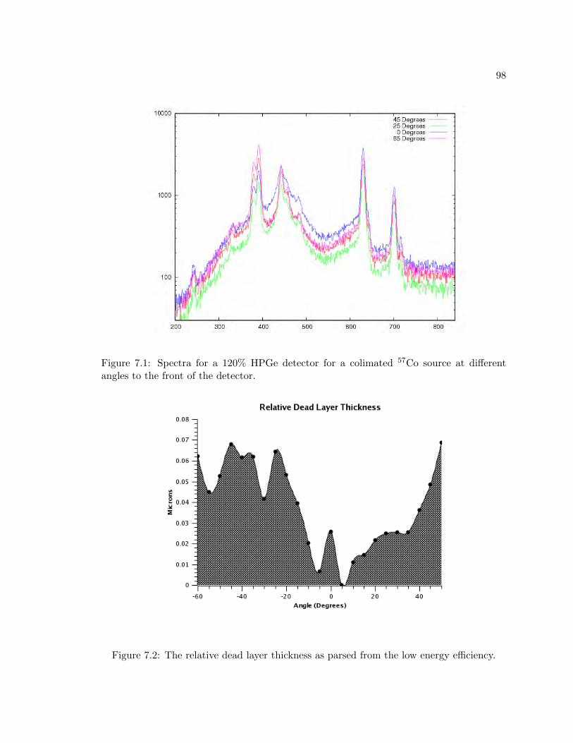
98
Figure 7.1: Spectra for a 120% HPGe detector for a colimated 57Co source at differentangles to the front of the detector.
Figure 7.2: The relative dead layer thickness as parsed from the low energy efficiency.

99
Figure 7.3: Rise time data extracted from the 122 keV peak of the 57Co spectra.
for each angle relative to some well chosen reference position. For this measurement we chose
5 as the relative angle since it gave the thinest dead layer, all other angle measurements
are the thickness in addition the thickness at 5. The results of the dead layer uniformity
are given in Fig. 7.2.
Table 7.1: Mass attenuation Coefficients, density, and thicknesses for the materialsused in the measurement [5]. Dead layer thicknesses are typically ”several hunderedmicrometers”[6].
Mass attenuation Coefficients of the materials involvedMaterial Attenuation Density Thickness
Coefficient[cm2/g] [g/cm3] [cm]
Aluminum 0.155 2.702 0.050Germanium 0.405 5.3234 ≈ 0.02
Correcting for the dead layer of the detector we can fit a Gaussian peak to the
charge collection time of the given energy peak, as in Fig. 7.4, to extract the charge

100
Figure 7.4: A fit to the rise time extracted from the 122 keV peak of the 57Co spectra at25.
Figure 7.5: The timing for full charge collection of electrons in a p-type HPGe versus angle.The error bars indicate the FWHM of the peak.

101
Figure 7.6: The velocity of holes in a p-type HPGe versus angle. Including corrections fordead layer thickness.

102
collection time. Comparing these charge collection peaks we see the difference in the total
charge collection time as illustrated in Fig. 7.3. We can see the difference in the time it
takes for the different angles for a p-type semi-coaxial HPGe detector is maximally about
15 ns from Fig. 7.5. Using the results of these fits the dead layer thickness, relative to 5,
and timing information for each angle we can reconstruct the anisotropic drift velocity of
the charge carriers versus the angle in Fig. 7.6.
The effect of the anisotropic drift velocity of the charge carriers for an 80 mm p-
type semi-coaxial HPGe detector was measured. The maximal difference in the timing for
different angles was approximately 15 ns. When the Aalseth PSD method was applied to
multiple angular data sets, the difference in the PSD spaces were below the noise threshold.
Thus, for this detector it is determined that no angular information can be extracted with
this PSD method. Given the design of this detector it is unlikely that angular information
can be extracted, using this PSD method, from any semi-coaxial HPGe detector.
7.4 Effect of Finite Carrier Lifetimes
The charge carrier path lengths for a PPC can be significantly longer than those in
a semi-coaxial detector. The maximum length a charge carrier will move in a semi-coaxial
detector is from the outer radius to the inner radius. In a PPC where the height is roughly
equal to the radius then 13 of the volume of the crystal has a path length further then the
maximum path length in a semi-coaxial detector. If the height of the PPC is roughly equal
to the diameter, then the approximately 43 of the volume of the crystal extends beyond the
maximum path length of an equivalent semi-coaxial detector. Given that PPC detectors
come in various lengths, the volume that extends beyond the maximum path length of an
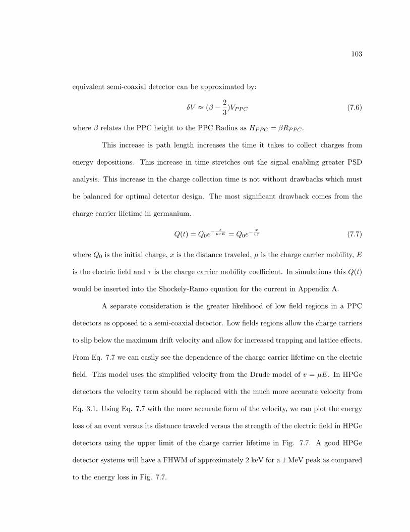
103
equivalent semi-coaxial detector can be approximated by:
δV ≈ (β − 23
)VPPC (7.6)
where β relates the PPC height to the PPC Radius as HPPC = βRPPC .
This increase is path length increases the time it takes to collect charges from
energy depositions. This increase in time stretches out the signal enabling greater PSD
analysis. This increase in the charge collection time is not without drawbacks which must
be balanced for optimal detector design. The most significant drawback comes from the
charge carrier lifetime in germanium.
Q(t) = Q0e− xµτE = Q0e
− xvτ (7.7)
where Q0 is the initial charge, x is the distance traveled, µ is the charge carrier mobility, E
is the electric field and τ is the charge carrier mobility coefficient. In simulations this Q(t)
would be inserted into the Shockely-Ramo equation for the current in Appendix A.
A separate consideration is the greater likelihood of low field regions in a PPC
detectors as opposed to a semi-coaxial detector. Low fields regions allow the charge carriers
to slip below the maximum drift velocity and allow for increased trapping and lattice effects.
From Eq. 7.7 we can easily see the dependence of the charge carrier lifetime on the electric
field. This model uses the simplified velocity from the Drude model of v = µE. In HPGe
detectors the velocity term should be replaced with the much more accurate velocity from
Eq. 3.1. Using Eq. 7.7 with the more accurate form of the velocity, we can plot the energy
loss of an event versus its distance traveled versus the strength of the electric field in HPGe
detectors using the upper limit of the charge carrier lifetime in Fig. 7.7. A good HPGe
detector systems will have a FHWM of approximately 2 keV for a 1 MeV peak as compared
to the energy loss in Fig. 7.7.

104
Figure 7.7: A plot of the charge carrier lifetime limit in high purity germanium at 77 kversus path length and electric field strength. This is for holes and is the loss of energygiven a 1 MeV energy deposition with τ < 1E − 4 seconds [6].

105
Based on this simple model, we can measure the charge carrier loss of a given energy
if we can establish the distance the charge traveled. For semi-coaxial HPGe detectors, this
correction would be insignificant except for crystals with significant lattice damage and
trapping regions. For a PPC detector, however, the path lengths of the charge carriers
can give rise to significant energy losses due to even a reasonable charge carrier lifetime.
The two requirements for this type of measurement are that, first, we can identify events
belonging to a specific full energy deposition even with charge trapping losses. Using a
coincidence γ-source we can easily identify the energy of the deposition. Second, we must
be able to identify the distance which the charge carrier has traveled.
A PPC detector has a very different pulse shape from a semi-coaxial detector.
One major difference is that for a PPC pulse, the start time is often unknown. However, if
we place a NaI detector in coincidence with the PPC detector for a 60Co γ-source we can
measure the start time of the pulse independently of the PPC detector. We compare the
total charge carrier lifetime measured by the NaI detector to the 10− 90% rise time of the
PPC detector. Fig. 7.8 thus verifies the simple linear relationship between the total drift
time to the 10− 90% rise time of the PPC detector. The first implication is that if a drift
time correction is necessary, then it can be done for this and similar PPC detectors. The
second implication is that the 10 − 90% rise time of a PPC pulse carries spatial and drift
time information for the entire volume.
A measure of the charge carrier lifetime for the UC PPC detector was made using
the 60Co coincident data set. By fitting an energy peak versus the 10 − 90% rise time,
as in Fig. 7.9, we can demonstrate the effect of the charge carrier lifetime on the energy
peak through its losses. Fig. 7.9 graphs the energy peaks versus rise time at depletion

106
Figure 7.8: A plot of the total charge carrier drift time in the UC PPC versus the 10-90%rise time of the integrated current pulse. For the 1332.5 keV gamma of a 60Co source taggedwith a NaI detector. Data courtesy of Phil Barbeau and Juan Collar at the University ofChicago.
(2500 Volts) as well as at the operating voltage (3000 Volts). The charge carrier lifetime
measured is 1.654E − 4 s at 2500 Volts and 0.878E − 4 s at 3000 Volts, demonstrating the
need for significant electric field strengths in the PPC detector.
7.5 Optimizing a Geometry
Combining the models with a Monte Carlo we can evaluate the figure of merit for
different HPGe radii and height given the same impurity density. The figure of merit to be
used has previously been defined in in chapter 4 folowing from that developed by Aalseth
[67]. We show the geometry space below and the results of the figure of merit calculations
using a 228Th source distributed uniformly around the detector.

107
Figure 7.9: A plot of the Energy versus the duration for the UC PPC.

108
Figure 7.10: Representation of the geometric parameter space. We can see the change indiameter and height for the parameter space in question.
The parameter space consists only of the diameter and height of a P-type Point
Contact detector. This parameter space is illustrated in Fig. 7.10. The point contact itself
is 6mm in diameter. The impurity density equation is
ρ(r, z) = A+Br + Cz (7.8)
Where A is −100E−5 Cm3 , B is 200E−5 C
m3 and C is 1000E−5 Cm3 . This choice allows the
entire range of diameters and heights to easily be depleted under 4000 volts. Each detector
had a dead layer thickness of 0.5 mm over the entire surface except the bottom passivated
surface. The thorium source surrounds the detector on all sides without any absorbing
material. The source include the entire thorium decay chain.
The depletion voltage for each detector was solved given the the impurity density.
Each detector was simulated at 500 Volts above depletion. This gives a fairly uniform
electric field throughout the detector except very close to the point contact. The potential
and electric field for each detector is then stored from later use.
Once the detector geometries were defined a Monte Carlo of the radiation inter-
actions for each detector geometry was performed. The data listed each energy deposition

109
as part of the parent event. Each event corresponds to a single iteration through the entire
decay chain. Thus no two independent decays can interfere as background or summing.
Each energy deposition has an interaction time relative to the parent event. In the
charge transport simulation all energy depositions are simulated with the given location and
relative timing. The signals are recorded and passed through the electronics transfer func-
tion into the appropriate file format for analysis. Thus very realistic signals are generated
for analysis by the same code used to analyze experimental data.
The analysis is a pulse by pulse based parametric method developed in the IGEX
experiment [73, 9, 65]. The code uses a training set of predominately single site events.
Thus a single site event library can be fed directly into the analysis code, or one can use
the events from a given energy whose interactions are predominately single site. In this
case events from the 1592 keV peak have been shown to be > 90 percent single site through
Monte Carlo simulations [65]. Using these events from the energy peak to train the analysis
code, we can evaluate our ability to discriminate background, in this case the 1620 keV peak
is dominated by multiple site events, also show by Monte Carlo simulations, as seen in Fig.
7.11. This method is used to evaluate the efficacy of the pulse shape discrimination method
for an experiment with similar event interaction characteristics. The resulting figure of
merit for the geometric parameter space (Fig. 7.10) is presented in Fig. 7.12.

110
Figure 7.11: A 232Th spectrum illustrating the PSD method used to remove most of themultiple site events while retaining most of the single site events. Using these peaks fromthis type of spectrum follows the method outlined in [9].

111
Figure 7.12: The resulting figure of merit interpolated for the geometric parameter spaceshown in Fig. 7.10 of different radii and heights for a simple Point Contact Detector design.

112
Chapter 8
Conclusion
8.1 Overview
Physicists have and will continue to explore the nature of the neutrino through
a variety of experimental techniques [15, 13, 82, 32]. Neutrino-less double beta decay is a
process specific to certain fundamental properties of the neutrino [12, 83, 20]. Experiments
must continue to improve beyond present detector sensitivity in order to explore these
properties. Advancement is required in many areas to achieve this lofty goal, detector
design optimization is one such necessary advancement [84, 14, 20]. This work does not
address the requirements of any specific experiment, instead it addresses the key components
and develops the necessary models to optimize HPGe detector design parameters to meet
experiment specific goals.
Many neutrino-less double beta decay experiments employ isotropically enriched
high purity germanium detectors as both source and detector [20, 73, 23, 22]. For greatest
sensitivity these experiments must build a detector that maximizes the 0νββ-signal while

113
simultaneously minimizing backgrounds and noise. If a background free condition can be
obtained in the signal region within a width determined by the energy resolution, the
sensitivity scales as the square root of the exposure [14]. Great efforts have gone into
eliminating sources of radioactive contamination [41, 42, 43, 44, 24, 85, 86] via extreme
shielding [12], evaluation and screening of all material [87], minimalistic suspension and
contact design [22], the use of ultra-pure materials [27] and pulse shape analysis [65, 62, 88,
89].
A factor of 1.56 in the half life sensitivity by pulse shape analysis has been demon-
strated [90], further an increase from electrical contact segmentation has also been demon-
strated [62, 91]. Novel electrical contact design has also shown increase in half-life sensitivity
[8]. Clearly that the sensitivity to the neutrino-less double beta decay signal in these ex-
periments is greatly affected by many factors of the detector design and subsequent signal
analysis. To truly maximize experiment efficacy, each experiment must seek an optimal
detector design and operational parameters based on both initial experimental conditions
and ultimate scientific goals.
In this work, models for electric field, charge transport, and signal formation are
developed given an electrode geometry description, charged impurity density equation, and
electrical response function as input parameters. A novel detector characterization is pre-
sented to address the difficulty of characterizing the charge impurity equation, with exper-
imental validation. A pulse shape analysis method is also developed from previous work.
The combination of these elements provides a robust evaluation of detector design and
operational parameters impact on the specific goals of an experiment.
Highlights of the computer code are explained, including the geometrical repre-

114
sentations, electrostatic solutions and signal generation dynamics. The code includes func-
tionality for including the electrical response, nevertheless this work uses a general HPGe
preamplifier response function from the appropriate literature. Results are shown to pass a
series of systematic and experimental validations. The importance of the charged impurity
profile to this model requires its characterization beyond current standards or even capa-
bilities. A method is presented to iteratively solve for the charged impurity profile within
the error of a χ2 fit [51] using the measured capacitance as a function of voltage. Chapter
6 shows an example of this technique.
We provide a simple example of one possible use of this model for the optimization
of input parameters for some defined experimental result. We use a simple equation for the
charged impurity equation, combined with the contact geometry of a p-type point contact
detector. Reasonable limits were set on the allowed depletion voltages and detector size
were used. The a figure of merit for a well defined physics goal was used to find the optimal
diameter and height combination given the simulation limits.
8.2 Extension of this work to future 0νββ decay experiments
Great efforts have gone into eliminating sources of radioactive contamination [41,
42, 43, 44, 24, 85, 86] via extreme shielding[12], evaluation and screening of all material [87],
minimalistic suspension and contact design [22], the use of ultra-pure materials [27] and
pulse shape analysis [65, 62, 88, 89]. Radiation transport and Monte Carlo simulations may
be used to study the effects of material radio-purity and spatial distribution of radioactive
sources within an experimental geometry. The data from these Monte Carlo simulations
can then be used to couple in detector design and property limits such as impurity density

115
Figure 8.1: Parameterized model for for simulation of the detector response.
116
and charge carrier lifetime. The final step of applying the actual analysis methods directly
to the simulation data will allow a realistic evaluation of the total detector design toward
the science specific goals.
Our model simulates the response of high purity germanium detectors to radiation
based on a large set of physical parameters. This parameter set includes the geometry, the
electrode layout, the charged impurity density and even the electronics response. The model
will evaluate any parameter set from simulated radiation event data completely through to
the specific analysis performed on the data. Given quantifiable experiment specific goals,
this entire model can be used to evaluate many possible parameter sets. This model even
allows the optimization of the input parameters to achieve maximum efficiency in some
appropriate experiment specific goals.
Neutrino-less double beta decay experiments will have a certain set of well defined
goals for experiential success embodied in an appropriately defined figure of merit. The
model can be used to optimize increasingly complex parameter spaces, within the limits
set, for a maximal probability of positive outcome for this defined set of physics goals. In
the case of Germanium detector experiments, at least two major experiments explore a
number of alternate designs in an attempt to identify the optimal strategy for experiments
scalable to one ton or more of active germanium mass. This huge undertaking will be
substantially aided by the analysis tools we have developed.
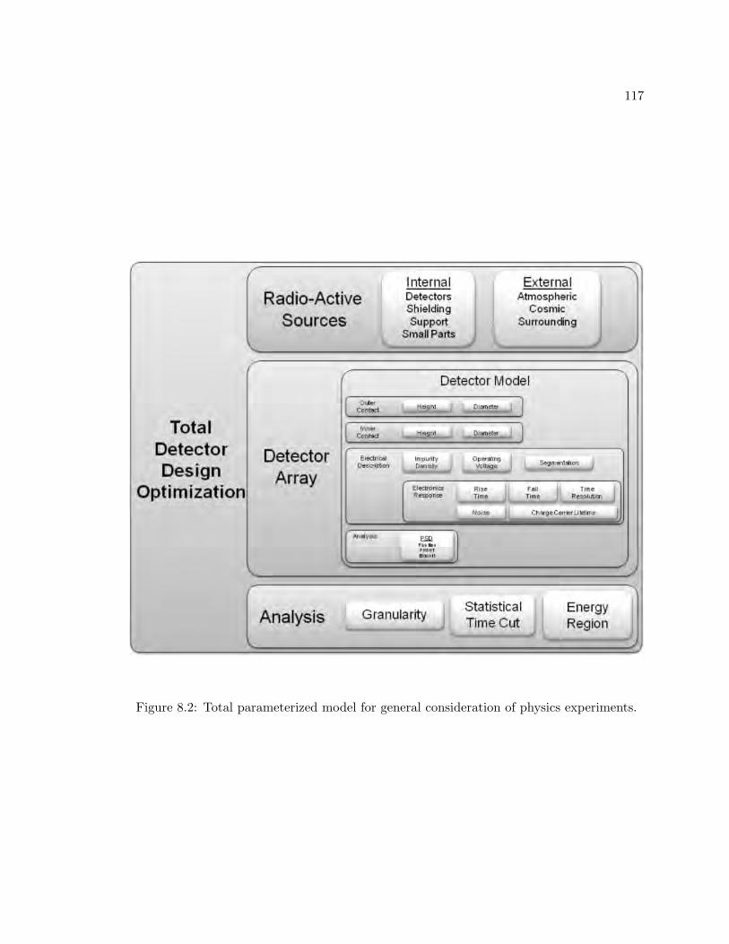
117
Figure 8.2: Total parameterized model for general consideration of physics experiments.

118
Bibliography
[1] M. Gunther, J. Hellmig, G. Heusser, M. Hirsch, H. V. Klapdor-Kleingrothaus, B. Maier,
H. Pas, F. Petry, Y. Ramachers, H. Strecker, M. Vollinger, A. Balysh, S. T. Belyaev,
A. Demehin, A. Gurov, I. Kondratenko, D. Kotel’nikov, V. I. Lebedev, and A. Muller.
Heidelberg-Moscow ββ experiment withˆ76 Ge: Full setup with five detectors. Phys-
ical Review D, 55(1):54–67, Jan 1997.
[2] Vadim Siklitsky. Band structure and carrier concentration.
http://www.ioffe.ru/SVA/NSM/Semicond/Ge/index.html.
[3] FA Trumbore. The Bell system technical journal, 1960.
[4] C. Canali, G. Majni, R. Minder, and G. Ottaviani. Electron and hole drift velocity
measurements in silicon and their empirical relation to electric field and temperature.
IEEE Transactions on Electron Devices, 22(11):1045–1047, 1975.
[5] J.H. Hubbell and S. M. Seltzer. X-ray mass attenuation coefficients.
http://physics.nist.gov/PhysRefData/XrayMassCoef/tab3.html, April 1996.
[6] Glenn F. Knoll. Radiation Detection and Measurment. Wiley, 2000.

119
[7] E.E. Haller, W.L. Hansen, and F.S. Goulding. Physics of ultra-pure germanium. Ad-
vances in Physics, 30(1):93–138, 1981.
[8] J. I. Collar P. S. Barbeau and O. Tench. Large-mass ultra-low noise germanium detec-
tors: Performance and applications in neutrino and astroparticle physics. arXiv:nucl-
ex/0701012v1, 2007.
[9] H.S. Miley C.E. Aalseth. A novel method of pulse shape discrimination for germanium
spectrometers. Nuclear Physics B - Proceedings Supplements, 2000.
[10] S. M. Bilenky, S. Pascoli, and S. T. Petcov. Majorana neutrinos, neutrino mass spec-
trum, cp violation, and neutrinoless double β decay: The three-neutrino mixing case.
Phys. Rev. D, 64(5):053010, Aug 2001.
[11] H.S. Miley. Majorana whitepaper. Technical report, PNNL, 2005.
[12] F.T. Avignone III, S.R. Elliott, and J. Engel. Double Beta Decay, Majorana Neutrinos,
and Neutrino Mass. eprint arXiv: 0708.1033, 2007.
[13] S.R. Elliott and J. Engel. Double-beta decay. J. Phys, 30:183–215, 2004.
[14] S.R. Elliott. Introduction to the Double-Beta Decay Experimental Program. Arxiv
preprint nucl-ex/0609024, 2006.
[15] A. Barabash. Double beta decay experiments: past and present achievements. Arxiv
preprint hep-ex/0608054, 2006.
[16] F. Boehm and P. Vogel. Physics of Massive Neutrinos. New York: Cambridge, 1992.
[17] B. Kayser. On the quantum mechanics of neutrino oscillation. Physical Review D,
24(1):110–116, 1981.

120
[18] Z. Xing, FR Klinkhamer, A. Kostelecky, J. Tasson, M. Pospelov, A. Ritz, S. Winitzki,
R. Whisker, S.D.O. Shin’ichi Nojiri, M. Kawasaki, et al. Theoretical Overview of
Neutrino Properties. International Journal of Modern Physics A, 23(26):4255–4272,
2008.
[19] RN Mohapatra, S. Antusch, KS Babu, G. Barenboim, MC Chen, S. Davidson,
A. de Gouvea, P. de Holanda, B. Dutta, Y. Grossman, et al. Theory of Neutrinos:
A White Paper. Reports on Progress in Physics, 70(11):1757–1867, 2007.
[20] A. Morales and J. Morales. The neutrinoless double beta decay: The case for germa-
nium detectors. Nuclear Physics B (Proceedings Supplements), 114:141–157, 2003.
[21] C. E. Aalseth, F. T. Avignone, R. L. Brodzinski, J. I. Collar, E. Garcia, D. Gonzalez,
F. Hasenbalg, W. K. Hensley, I. V. Kirpichnikov, A. A. Klimenko, H. S. Miley,
A. Morales, J. Morales, A. Ortiz de Solorzano, S. B. Osetrov, V. S. Pogosov,
J. Puimedon, J. H. Reeves, A. Salinas, M. L. Sarsa, A. A. Smolnikov, A. S. Starostin,
A. G. Tamanyan, A. A. Vasenko, S. I. Vasiliev, and J. A. Villar. Neutrinoless double-
beta decay of 76Ge: First results from the International Germanium Experiment
(IGEX) with six isotopically enriched detectors. Phys. Rev. C, 59(4):2108–2113, Apr
1999.
[22] A. Bettini. GERDA. Germanium Detector Array. Search for Neutrino-less ββ Decay
of 76Ge. Nuclear Physics B (Proceedings Supplements), 168:67–69, 2007.
[23] R. Arthur F.T. Avignone III C. Baktash T. Ball A. S. Barabash F. Bertrand R. L.
Brodzinski V. Brudanin W. Bugg A. E. Champagne Y-D. Chan T. V. Cianciolo J. I.
Collar R. W. Creswick M. Descovich M. Di Marco P. J. Doe G. Dunham Yu. Efremenko
121
V. Egerov H. Ejiri S. R. Elliott A. Emanue P. Fallon H. A. Farach R. J. Gaitskell1
V. Gehman R. Grzywacz A. Hallin R. Hazma R. Henning A. Hime T. Hossbach D.
Jordan K. Kazkaz J. Kephart G. S. King III O. Kochetov S. Konovalov R. T. Kouzes
K. T. Lesko P. Luke M. Luzum A. O. Macchiavelli A. McDonald D. Mei H. S. Miley
G. B. Mills A. Mokhtarani M. Nomachi J. L. Orrell J. M. Palms A. W. P. Poon D.
C. Radford J. H. Reeves R. G. H. Robertson R. Runkle K. Rykaczewski K. Saburov
Y. Sandukovsky Sonnenschein A. Tornow W. Tull C. van de Water R.G. Vanushin
I. Vetter K. Warner R.A C. E. Aalseth, D. Anderson, J.M. Young A.R Wilkerson,
J.F. Wouters, and V. Yumatov. The majorana experiment. Something, 2004.
[24] RL Brodzinski, HS Miley, JH Reeves, and FT Avignone. Low-background Germanium
spectrometry the bottom line three years later. Journal of Radioanalytical and Nuclear
Chemistry, 193(1):61–70, 1995.
[25] I. Abt, M. Altmann, A. Bakalyarov, I. Barabanov, C. Bauer, E. Bellotti, ST Belyaev,
L. Bezrukov, V. Brudanin, C. Buettner, et al. A New 76Ge Double Beta Decay Ex-
periment at LNGS. Arxiv preprint hep-ex/0404039, 2004.
[26] S. Schonert, I. Abt, M. Altmann, AM Bakalyarov, I. Barabanov, C. Bauer, M. Bauer,
E. Bellotti, S. Belogurov, ST Belyaev, et al. The GERmanium Detector Array (Gerda)
for the search of neutrinoless ββ decays of 76Ge at LNGS. Nuclear Physics B (Pro-
ceedings Supplements), 145:242–245, 2005.
[27] E.W. Hoppe, A. Seifert, C.E. Aalseth, A.R. Day, O.T. Farmer, T.W. Hossbach, J.I.
McIntyre, H.S. Miley, J.E. Smart, and G.A. Warren. A method for removing surface
122
contamination on ultra-pure copper spectrometer components. Journal of Radioana-
lytical and Nuclear Chemistry, 276(3):645–650, 2008.
[28] C. Amsler, M. Doser, M. Antonelli, DM Asner, KS Babu, H. Baer, HR Band, RM Bar-
nett, E. Bergren, J. Beringer, et al. Particle Data Group. Phys. Lett. B, 667(1), 2008.
[29] M. Lauer. Digital Signal Processing for Segmented HPGe Detectors Preprocessing Al-
gorithms and Pulse Shape Analysis. PhD thesis, s. n, 2004.
[30] L.P. Gamir. A new method for the determination of the entry position of γ rays in HPGe
detectors by current pulse analysis. PhD thesis, Max-Planck-Institut fur Kernphysik,
Heidelberg, 1997.
[31] K. Vetter. Gamma-ray tracking: Utilizing new concepts in the detection of gamma-
radiation. The European Physical Journal A-Hadrons and Nuclei, 15(1):265–269, 2002.
[32] K. Zuber. Neutrinoless double beta decay experiments. ACTA PHYS.POLON.B,
37:1905, 2006.
[33] G. Heusser. Low-Radioactivity Background Techniques. Annual Reviews in Nuclear
and Particle Science, 45(1):543–590, 1995.
[34] K.S. Krane. Introductory Nuclear Physics. John Wiley & Sons, 1987.
[35] K. Debertin and R.G. Helmer. Gamma-and x-ray spectrometry with semiconductor
detectors. North-Holland, 1988.
[36] S.N. Ahmed. Physics & Engineering of Radation Detection. Academic Press, 2007.
[37] Karl Hess. Advanced Theory Of Semiconductor Devices. PublisherWiley-Interscience,
1999.

123
[38] C. Kittel et al. Introduction to solid state physics. Wiley New York, 1986.
[39] J.D. Jackson. Classical Electrodynamics. Wiley, 1998.
[40] U. Fano. Ionization Yield of Radiations. II. The Fluctuations of the Number of Ions.
Physical Review, 72(1):26–29, 1947.
[41] R.L. Brodzinski, D.P. Brown, J.C. Evans, W.K. Hensley, J.H. Reeves, N.A. Wog-
man, F.T. Avignone, and H.S. Miley. An ultralow background germanium gamma-
ray spectrometer. Nuclear Instruments and Methods in Physics Research Section A,
239(2):207–213, 1985.
[42] RL Brodzinski, JH Reeves, FT Avignone, and HS Miley. Achieving ultralow back-
ground in a germanium spectrometer. Journal of Radioanalytical and Nuclear Chem-
istry, 124(2):513–521, 1988.
[43] RL Brodzinski, HS Miley, JH Reeves, and FT Avignone. Further reduction of radioac-
tive backgrounds in ultrasensitive germanium spectrometers. Nuclear Instruments and
Methods in Physics Research Section A, 292(2):337–342, 1990.
[44] RL Brodzinski, HS Miley, JH Reeves, and FT Avignone. Ultra-low background ger-
manium spectrometry: Techniques and results. Nuclear Physics B Proceedings Supple-
ments, 28(1):415–419, 1992.
[45] S.O. Kasap. Principles of Electrical Engineering Materials and Devices. McGraw-Hill,
2000.
[46] S. Ramo. Currents induced by electron motion. Proc. IRE, 27(9):584, 1939.

124
[47] W. Shockley. Currents to conductors induced by a moving point charge. Journal of
Applied Physics, 9:635, 1938.
[48] G. Cavalleri, E. Gatti, G. Fabri, and V. Svelto. Extension of ramos theorem as applied
to induced charge in semiconductor detectors. Nucl. Instr. and Meth, 92:137–140, 1971.
[49] S. Prata. C++ Primer Plus. Sams Publishing, 2001.
[50] Radika. Noise in radiation detection. Reviews of Physics, 1982.
[51] W.H. Press, S.A. Teukolsky, W.T. Vetterling, and B.P. Flannery. Numerical recipes in
C++. Cambridge University Press New York, 2002.
[52] L. Reggiani, C. Canali, F. Nava, and G. Ottaviani. Hole drift velocity in germanium.
Physical Review B, 16(6):2781–2791, 1977.
[53] W. Shockley. Currents in conductors induced by moving point charge. Journal of
Applied Physics, 1938.
[54] CE Aalseth and HS Miley. A simulation method for germanium pulse shapes. Nuclear
Science Symposium, 1999. Conference Record. 1999 IEEE, 2, 1999.
[55] Z. He. Review of the shockley–ramo theorem and its application in semiconductor
gamma-ray detectors. Nuclear Inst. and Methods in Physics Research, A, 463(1-2):250–
267, 2001.
[56] A. Vladimirescu. The SPICE book. J. Wiley New York, 1994.
[57] H.S. Miley C.E. Aalseth. A simulation method for germanium pulse shapes. IEEE
Nuclear Science Symposium Conference Record, 1999.

125
[58] H. Spieler. Semiconductor Detector Systems. Oxford University Press, 2005.
[59] G. Douysset, T. Fritioff, C. Carlberg, I. Bergstrom, and M. Bjorkhage. Determination
of theˆ76 Ge Double Beta Decay Q Value. Physical Review Letters, 86(19):4259–
4262, 2001.
[60] R.B. Firestone, V.S. Shirley, C.M. Baglin, S.Y.F. Chu, and J. Zipkin. Table of isotopes.
Wiley, 1996.
[61] L. Pandola, M. Bauer, K. Kroninger, X. Liu, C. Tomei, S. Belogurov, D. Franco,
A. Klimenko, and M. Knapp. Monte Carlo evaluation of the muon-induced background
in the GERDA double beta decay experiment. Nuclear Inst. and Methods in Physics
Research, A, 570(1):149–158, 2007.
[62] I. Abt, M. Altmann, A. Caldwell, K. Kroninger, X. Liu, B. Majorovits, L. Pandola,
and C. Tomei. Background reduction in neutrinoless double beta decay experiments
using segmented detectorsA Monte Carlo study for the GERDA setup. Nuclear Inst.
and Methods in Physics Research, A, 570(3):479–486, 2007.
[63] R.A. Fisher. On the Mathematical Foundations of Theoretical Statistics. 1992). Break-
throughs in Statistics, 1, 1922.
[64] G. Vasilescu. Electronic Noise And Interfering Signals: Principles And Applications.
Springer, 2005.
[65] C.E. Aalseth. Germanium Spectrometer Pulse-shape Discrimination for 76Ge Double-
beta Decay. PhD thesis, University of South Carolina, 2000.

126
[66] TOC View. IEEE standard test procedures for high-purity germanium crystalsfor
radiation detectors. IEEE Std 1160-1993, 1993.
[67] C.E. Aalseth. Germanium spectrometer pulse-shape discrimination for germanium-76
double-beta decay. PhD thesis, UNIVERSITY OF SOUTH CAROLINA, 2001.
[68] PN Luke, FS Goulding, NW Madden, and RH Pehl. Low capacitance large volume
shaped-field germanium detector. Nuclear Science, IEEE Transactions on, 36(1):926–
930, 1989.
[69] J. L. Orrell, C. E. Aalseth, M. W. Cooper, J. D. Kephart, and C. E. Seifert. Radial
position of single-site gamma-ray interactions from a parametric pulse shape analysis
of germanium detector signals. Presented at the SORMA XI Conference, Ann Arbor,
MI, May 2006.
[70] MA Deleplanque, IY Lee, K. Vetter, GJ Schmid, FS Stephens, RM Clark, RM Dia-
mond, P. Fallon, and AO Macchiavelli. Greta: Utilizing new concepts in-ray detection.
Nuclear Instruments and Methods in Physics Research A, 430:292–310, 1999.
[71] IY Lee, RM Clark, M. Cromaz, MA Deleplanque, M. Descovich, RM Diamond, P. Fal-
lon, AO Macchiavelli, FS Stephens, and D. Ward. GRETINA: A gamma ray energy
tracking array. Nuclear Physics, Section A, 746:255–259, 2004.
[72] Jeremy Kephart. Method of evaluating the effect of HPGe design on the sensitivity of
physics experiments. PhD thesis, North Carolina State University, 2009.
[73] CE Aalseth, FT Avignone III, RL Brodzinski, S. Cebrian, E. Garcia, D. Gonzalez,
WK Hensley, IG Irastorza, IV Kirpichnikov, AA Klimenko, et al. IGEXˆ76 Ge

127
neutrinoless double-beta decay experiment: Prospects for next generation experiments.
Physical Review D, 65(9):92007, 2002.
[74] P.N. Luke. Low noise germanium radial drift detector. Nuclear Instruments and Meth-
ods in Physics Research Section A, 271(3):567–570, 1988.
[75] PN Luke. Germanium Detectors with a Built-In Transverse Drift Field. IEEE Trans.
Nucl. Sci, 32(1), 1985.
[76] Juan Collar. Private communication. email.
[77] IY Lee. Gamma-ray tracking detectors. Nuclear Instruments and Methods in Physics
Research Section A: Accelerators, Spectrometers, Detectors and Associated Equipment,
422(1):195–200, 1999.
[78] K. Vetter, A. Kuhn, MA Deleplanque, IY Lee, FS Stephens, GJ Schmid, D. Beckedahl,
JJ Blair, RM Clark, M. Cromaz, et al. Three-dimensional position sensitivity in two-
dimensionally segmented HP-Ge detectors. Nuclear Inst. and Methods in Physics Re-
search, A, 452(1-2):223–238, 2000.
[79] C. Jacoboni and P. Lugli. The Monte Carlo method for semiconductor device simula-
tion. Springer, 1989.
[80] D.K. Schroeder. Semiconductor material and device characterization. Wiley, 1990.
[81] Craig Aalseth. Private communication. email.
[82] RN Mohapatra, S. Antusch, KS Babu, G. Barenboim, M.C. Chen, S. Davidson,
A. de Gouvea, P. de Holanda, B. Dutta, Y. Grossman, et al. Theory of Neutrinos:
A White Paper. Arxiv preprint hep-ph/0510213, 2005.

128
[83] P. Vogel. Double Beta Decay: Theory, Experiment, and Implications. Arxiv preprint
nucl-th/0005020, 2000.
[84] I. Abt, A. Caldwell, K. Kroninger, J. Liu, X. Liu, and B. Majorovits. Identification of
photons in double beta-decay experiments using segmented germanium detectorsStud-
ies with a GERDA phase II prototype detector. Nuclear Inst. and Methods in Physics
Research, A, 583(2-3):332–340, 2007.
[85] H. Gomez, S. Cebrian, J. Morales, and J. A. Villar. Background reduction and sensi-
tivity for germanium double beta decay experiments, 2007.
[86] HS Miley, RL Brodzinski, WK Hensley, JH Reeves, and FT Avignone. New techniques
and results in sup 76 Ge double-beta decay. Conference: 2. international workshop
on theoretical and phenomenological aspects of underground physics, Toledo (Spain),
9-13 Sep 1991, 1991.
[87] FT Avignone, RL Brodzinski, JI Collar, HS Miley, E. Garcia, A. Morales, J. Morales,
R. Nunez-Lagos, JH Reeves, C. Saenz, et al. Theoretical and experimental investigation
of cosmogenic radioisotope production in germanium. Nuclear Physics B Proceedings
Supplements, 28(1):280–285, 1992.
[88] D. Gonzalez, J. Morales, S. Cebrian, E. Garcıa, IG Irastorza, A. Morales, A. Ortiz de
Solorzano, J. Puimedon, ML Sarsa, JA Villar, et al. Pulse-shape discrimination in the
IGEX experiment. Nuclear Inst. and Methods in Physics Research, A, 515(3):634–643,
2003.
[89] HV Klapdor-Kleingrothaus, IV Krivosheina, and IV Titkova. Theoretical investigation
of the dependence of double beta decay tracks in a Ge detector on particle and nu-

129
clear physics parameters and separation from gamma ray events. Physical Review D,
73(1):13010, 2006.
[90] CE Aalseth and HS Miley. The Majorana Project: Ge-76 0νββ-decay neutrino mass
measurement. Nuclear Physics B-Proceedings Supplements, 110:392–394, JUL 2002.
[91] SR Elliott, VM Gehman, K. Kazkaz, D.M. Mei, and AR Young. Pulse shape analysis in
segmented detectors as a technique for background reduction in Ge double-beta decay
experiments. Nuclear Inst. and Methods in Physics Research, A, 558(2):504–510, 2006.

130
Appendices

131
Appendix A. Shockely Ramo theorem for calculation
Consider the equation for the total rate of work done by the fields given a contin-
uous distribution of charge and current in a finite volume: (Eq. 6.103 [39])∫τ
E · Jtdτ (A-1)
where Jt = J + ∂D∂t such that ∇ · Jt = ∇(J + ∂D
∂t ) = 0. Let us assume a quasi-static case:
E = −∇φ (A-2)
We can write the current equation:∫τ
E · Jtdτ =∫τ−∇φ · Jt = −
∫τ∇ · (φJt)dτ +
∫τφ∇ · Jtdτ (A-3)
The last term is equal to zero. We can apply the divergence theorem to the next to the
remaining term to get:∫τ
E · (J +∂D∂t
)dτ = −∫SφJ · dS =
n∑k=1
VkIk(t) (A-4)
with Vk as the voltage applied to the kth electrode and Ik(t) is the current on the kth
electrode. We can separate out the relevant parts by the principle of linear super position
such that E = E1 + E2 + E3 with E1 being the electric field due to the electrodes with no
space charge, E2 is due to static space charge ρ2 and E3 is due to the moving charge ρ3
with a velocity u3. Note that ρ = ρ2 + ρ3, such that the boundaries are at zero potential
due to the presence of charge. φ1(r → S) = Vk and φ2(r → S) = φ3(r → S) = 0 at all
electrodes.
Let Vk → 0 for all k, while retaining ρ2 and ρ3.∫τ
E · (J +∂D∂t
)dτ =∫
(E2 + E3) · (ρ3u +∂
∂t(D2 + D3))dτ = 0 (A-5)

132
where D2 = εE2 and D3 = εE3. Then:
∂D1
∂t= 0 =
∂D2
∂t(A-6)
We write E2 + E3 = E−E1 to get
∫(E−E1 · (ρ3u +
∂D3
∂t)) = 0 (A-7)
⇒∫
E · (ρ3u +∂D3
∂t)dτ =
n∑k=1
VkIk(t) =∫
E1 · (ρ3u +∂D3
∂t)dτ (A-8)
Such that:n∑k=1
VkIk(t) =∫
E1 · (ρ3u +∂D3
∂t)dτ (A-9)
Taking the second term in the integral
∫E1 ·
∂D3
∂tdτ (A-10)
Using
∂
∂t
∫E1 ·D3dτ =
∫∂E1
∂t·D3dτ +
∫E1 ·
∂D3
∂tdτ (A-11)
We can see that ∫∂E1
∂t·D3dτ = 0 (A-12)
Since E1 is constant in time, we can pull the partial differential outside of the integral to
get: ∫E1 ·
∂D3
∂tdτ =
∂
∂t
∫E1 ·D3dτ (A-13)
We can use the definition of D3 = εE3 to write:
∫E1 ·
∂D3
∂tdτ =
∂
∂tε
∫E1 ·E3dτ (A-14)

133
We can then use the relationship of the electric field to the potential E = −∇φ to write:
∫E1 ·
∂D3
∂tdτ =
∂
∂tε
∫∇φ1 · ∇φ3dτ (A-15)
Using Green’s first identify [39]
∫τ(φ3∇2φ1 +∇φ1 · ∇φ3)dτ =
∮Sφ3 ·
∂φ1
∂tdS (A-16)
From this equation we know that ∇2φ1 = ρ1 = 0, as well we have φ3 = 0 at the surface. So
this part of the integral is zero. We are left with:
n∑k=1
VkIk(t) =∫
(E1 · ρ3u)dτ) (A-17)
With the applied voltage on electrode k being Vk we can divide through to get the current
Ik(t):
Ik(t) =∫
(Wk1 · ρ3u)dτ) (A-18)
where Wk1 = E1Vk
is the weight potential. Thus we are left with the current on electrode k
as a function of time due to the movement of the charge ρ3, the applied voltage on electrode
k and the electric field due to the electrodes with no space charge.