abstract document: complex metal oxide thin film growth by
TRANSCRIPT
ABSTRACT
Title of Document: COMPLEX METAL OXIDE THIN FILM GROWTH BY METALORGANIC CHEMICAL VAPOR DEPOSITION
Seung-Yeul Yang, Doctor of Philosophy, 2005
Directed By: Professor Ramamoorthy Ramesh,
Department of Materials Science and Engineering
The phenomenon of ferroelectricity recently attracted great attention with the
successful advances in the development of thin-film fabrication. This development
enables the integration of ferroelectric materials directly into device fabrication
processes such as MEMS and FeRAMs. The stringent need for high-density, high-
speed, and low-power memory devices has prompted an immense interest in studying
the size effects in ferroic systems. The thickness dependence of ferroelectricity and
critical thickness, which is the thickness limit when the ferroelectricity disappears,
has become an issue of tremendous interest for both scientific and technological point
of view. In parallel, current nonvolatile memory manufacturing processes inevitably
require a scalable process such as metal-organic chemical vapor deposition
(MOCVD) to deposit the ferroelectric layers.
The process controls as well as the ferroelectric and piezoelectric properties of
two ferroelectric material systems, lead zirconate titanate (PZT) and bismuth ferrite

(BFO), prepared by MOCVD is presented in this dissertation. A systematic study on
deposition process control such as stoichiometric composition, structure change and
growth temperature was carried out.
The scaling of ferroelectric properties with film thickness in PZT films has
been investigated. PZT films show bulk-like properties for thickness above ~20 nm. It
was observed that a progressive decrease in the ferroelectric polarization as well as
the piezo-response as the thickness is decreased; films as thin as 3.6 nm are
piezoelectric. In this work, the interpretation of the origins of this decrease as well as
results of the MOCVD processing studies is studied.
Epitaxial BFO thin film, which is an interesting candidate for Pb-free ferro /
piezoelectrics, was grown by MOCVD as the first challenge. The film composition
and phase equilibrium are sensitive to the Bi:Fe supply ratio of precursors. In the
optimized condition, an epitaxial single perovskite phase thin films were obtained.
Electrical measurements using both quasi-static hysteresis and pulsed polarization
measurements confirm the existence of ferroelectricity with a switching polarization
of 110-120 µC/cm2, ∆P (= P* - P^). Out-of plane piezoelectric (d33) measurements
using an atomic force microscope yield a value of 50 – 55 pm/V.
COMPLEX METAL OXIDE THIN FILM GROWTH BY METALORGANIC CHEMICAL VAPOR DEPOSITION
By
Seung-Yeul Yang
Dissertation submitted to the Faculty of the Graduate School of the University of Maryland, College Park, in partial fulfillment
of the requirements for the degree of Doctor of Philosophy
2005
Advisory Committee: Professor Ramamoorthy Ramesh, Chair/Advisor Professor John N. Kidder, Jr. Professor Ichiro Takeuchi Professor Lourdes G. Salamanca-Riba Professor Raymond A. Adomaitis

© Copyright by Seung-Yeul Yang
2005

ii
DEDICATION
To my mother and father…
iii
ACKNOWLEDGEMENTS
First and foremost, I would like to express my sincere gratitude to my advisor,
Prof. R. Ramesh, for his support, patience, and encouragement throughout my Ph. D.
studies. His enthusiasm and the drive for the scientific pursuit were essential to the
completion of this dissertation and have taught me innumerable lessons and insights
on the research. I can never thank you enough to give me the opportunity to work on
this challenging and exciting project.
I also would like to thank my former advisor Prof. J. Kidder for introducing
me to the research of the metal oxide CVD. His guidance and assistance in getting my
research started on the right foot have led me to fruitful goal. I have benefited from
valuable discussions on design and set-up for the CVD system as well as the basic
theory on the thin film growth. This dissertation is part of the research carried out
through his vision throughout my research.
I am also grateful to Prof. L. Salamanca-Riba, Prof. I. Takeuchi and Prof. R.
Adomaitis for taking time out of their busy schedules to review my work.
I am fortunate to have the opportunity to work with intelligent and energetic
group collaborators, Dr. Florin Zavaliche, Dr. Tong Zhao, Ladan Mohaddes-Ardabili,
Dr. Haimei Zheng, Jun Ouyang, Junling Wang, Dr. Bao-Ting Liu, A. Prasertchoung,
and Dr. V. Nagarajan. Many parts of this dissertation would be impossible if it were
not for the collaboration with you and it is your friendships and invaluable
discussions that make the work for Ph. D. more precious.
I specially thank Dr. Florin Zavaliche for enlightening discussions on
ferroelectrics and constant encouraging during my research.

iv
I also want to show my gratitude to all the CONCEPT members at Berkeley
for giving me helpful suggestions and assistance.
Finally, I would like to thank my wife So-Young and my lovely daughter
Soomin for their understanding and love during my journey. Their support and
encouragement was in the end what made this dissertation possible. It would have
never been possible to have my research career without my parents' love, dedication
and their faith in me. I would like to thank my sisters and family for their love and
support. I own everything I achieved to them. This dissertation is dedicated to them.

v
TABLE OF CONTENTS
DEDICATION.............................................................................................................. ii
ACKNOWLEDGEMENTS......................................................................................... iii TABLE OF CONTENTS.............................................................................................. v LIST OF TABLES...................................................................................................... vii LIST OF FIGURES ................................................................................................... viii Chapter 1: Introduction ................................................................................................. 1
1.1 Ferroelectric materials ........................................................................................ 1 1.2 Pb(Zr,Ti)O3 ......................................................................................................... 4 1.3 Ferroelectric Random Access Memory (FeRAM)............................................ 10 1.4 Metal Organic Chemical Vapor Deposition (MOCVD)................................... 12 1.5 Theoretical analysis in ferroelectric films......................................................... 22
Chapter 2: Experimental techniques used in this study .............................................. 25
2.1 Precursors for PZT film growth........................................................................ 25 2.2 Liquid delivery system (LDS) MOCVD........................................................... 28
2.2.1 Lquid delivery system (LDS)..................................................................... 28 2.2.2 MOCVD system......................................................................................... 29
2.3 Conductive metal oxide thin film growth ......................................................... 32 2.3.1 RF sputtering.............................................................................................. 33 2.3.2 Pulsed laser deposition (PLD) ................................................................... 34
2.4 Device fabrication............................................................................................. 35 2.5 Characterization ................................................................................................ 37
2.5.1 X-ray Diffraction (XRD) ........................................................................... 37 2.5.2 Rutherford backscattering (RBS)............................................................... 38 2.5.3 Ferroelectric property characterization ...................................................... 40 2.5.4 Capacitance-Voltage measurement……………………………………….42
2.5.5 Piezoelectric force microscopy (PFM) …...………………………………42 Chapter 3: Pb(Zr0.5Ti0.5)O3 thin film growth on Si ..................................................... 45
3.1 Background ....................................................................................................... 45 3.2 Growth condition control.................................................................................. 47 3.3 Structural and electrical properties of Pb(Zr0.5Ti0.5)O3 films............................ 54 3.4 Comparison of piezoelectric properties of different thickness and composition................................................................................................................................. 63 3.5 Discussion ......................................................................................................... 67
Chapter 4: Thickness effects in epitaxial Pb(Zr,Ti)O3 films grown by MOCVD ...... 69
4.1 Background ....................................................................................................... 69

vi
4.2 Thickness effects in PZT thin films : a model system...................................... 73 4.3 The thickness effects in Pb(Zr0.2Ti0.8)O3 thin films .......................................... 80 4.4 Disccussion ....................................................................................................... 95
Chapter 5: BiFeO3 thin film growth by MOCVD...................................................... 97
5.1 Background ....................................................................................................... 97 5.2 Growth conditions............................................................................................. 99 5.3 Crystal structure .............................................................................................. 103 5.4 Surface morphology and Electrical properties................................................ 105 5.5 Discussion ....................................................................................................... 111
Chapter 6: Summary and future work...................................................................... 114

vii
LIST OF TABLES Table 2-1. Deposition parameters of PZT films prepared by liquid delivery
MOCVD………………………………………………………………..29 Table 5-1. Deposition parameters of BFO films prepared by liquid delivery
MOCVD………………………………………………………………..98

viii
LIST OF FIGURES
Figure 1-1. Hysteresis loop in ferroelectric materials…………………………………2 Figure 1-2. The phase diagram of PbZrO3 - PbTiO3 solid solution system…………...4 Figure 1-3. The ABO3 perovskite structure…………………………………………...6 Figure 1-4. (a) Ferroelectric and (b) Piezoelectric properties of Pb(Zr1-xTix)O3……...8 Figure 1-5. Trend of Cell Circuit Architecture and Cell Capacitor Structure……….10 Figure 1-6. SEM images of PZT film deposited on a patterned substrate…………...12 Figure 1-7. Cross-sectional SEM images. PZT films grown on (a) 17 µm wide (2 : 1
aspect ratio) and (b) 5 µm wide (6 : 1 aspect ratio) 3-D trench structures…………………………………….…………………………13
Figure 1-8. Chemical structure of (a) β-diketonates and (b) its complex (tetramethyl-heptanedionate (thd))….……………………………………………….17
Figure 1-9. Schematic diagram of MOCVD with conventional bubbler system…….18 Figure 1-10. Operation sequence in LDS MOCVD………………………………….20 Figure 2-1. The thermogravimetric (TG) curves show the good thermal compatible
behavior for Zr(dmhd)4 with Pb(thd)2 and Ti(OiPr)2(thd)2….…………25 Figure 2-2. Liquid line manifold……………………………………………………..26 Figure 2-3. The schematic of liquid delivery MOCVD system…………………...…28 Figure 2-4. The growth rate dependence of the liquid source supply rate…………...30 Figure 2-5. RF sputtering configuration.…………………………………………….31 Figure 2-6. Schematic of PLD system……………………………………………….33 Figure2-7. Sample structure after device fabrication………………………………...34 Figure 2-8. XRD measurement techniques…………………………………………..35 Figure 2-9. RBS result for a sample of PZT film on STO substrate…………………36 Figure 2-10. Signal drive profile for hysteresis polarization measurement………….37 Figure 2-11. Sequence of voltage pulses…………………………………………….38 Figure 2-12. Switching (P*) and non-switching (P^) polarization…………………...38 Figure 2-13. Schematic of the experimental setup for piezoelectric measurements…39 Figure 3-1. Growth of epitaxial STO films on Si substrate………………………….44 Figure 3-2. The relation of atomic percent of Pb, Zr and Ti of PZT films was
measured by RBS with precursor mixing ratio prepared at 650 oC and the same volume ratio (V(Pb) / V(Zr) = 1 ) of Pb and Zr precursors was used during deposition at 650 oC………………………………………45
Figure 3-3. The variation of Pb atomic percent grown at 650 oC with different liquid supply flow rate……………………………………….………………..47
Figure 3-4. The effect of Pb stoichiometry on ferroelectric properties of PZT films…………………………………………………………………....48
Figure 3-5. Composition dependence on growth temperature……………………….49 Figure 3-6. θ - 2θ XRD patterns from films deposited at different temperature…….50

ix
Figure 3-7. (a) P-E hysteresis loops and (b) Switched polarization (∆P = P* - Pr (~ 2Pr)) from films deposited at different temperature…………………...51
Figure 3-8. The dependence of oxygen flow rate on the film growth (a) O2 : 0 sccm and (b) O2 : 300 sccm. …………………………………………………52
Figure 3-9. A typical θ-2θ x-ray diffraction scan and φ-scan of LSCO/ PZT/LSCO capacitors deposited on STO/Si at 650 oC……………………………..53
Figure 3-10. The hysteresis response of 230 nm thick Pb(Zr0.5Ti0.5) capacitor sandwiched by LSCO electrodes at 1 V, 3 V and 5 V………………....54
Figure 3-11. Capacitance vs applied voltage measured with 230 nm thick Pb(Zr0.5Ti0.5) capacitor sandwiched by LSCO electrodes……………...55
Figure 3-12. Polarization (switched (P*) – non-switched (P^)) and coercive voltage of LSCO/PZT/LSCO capacitors as a function of applied voltage……..56
Figure 3-13. Pulse-width dependence of polarization (switched (P*) – non-switched (P^)) of LSCO/PZT/LSCO capacitors measured at 3V and 5 V, respectively………………………………………………………….…57
Figure 3-14. Fatigue resistant characteristics of LSCO/PZT/LSCO capacitors as a function of bipolar-pulsed cycles measured at 3 V and 5 V, respectively……………………………………………….……………58
Figure 3-15. Retention characteristics of LSCO/PZT/LSCO capacitors as a function of time measured at 3 V and 5 V, respectively………………………...59
Figure 3-16. Piezoelectric hysteresis loops of 230 nm and 1, 3, 5 µm-thick Pb(Zr0.5Ti0.5)O3 films…………………………………………………..60
Figure 3-17. The changes of piezoelectric coefficient (d33) and coercive field (Ec)with film thickness; d33 of PZT films, Ec of PZT films………….62
Figure 3-18. The changes of piezoelectric coefficient (d33) with change of Ti/(Zr+Ti) ratio; -♦- d33 of bulk PZT calculated by Haun et al., d33 of thin PZT obtained from MOCVD..……………………………………………....63
Figure 3-19. The variation of ferroelectric properties with change of Ti/(Zr+Ti) ratio; -•- Ps of bulk PZT calculated by Haun et al., Pr from MOCVD, Psfrom MOCVD, ♦ Pr from PLD, ◊ Pr from PLD, and ο Pr from Sputtering………………………………………………………….…...64
Figure 4-1. (a) Evolution of the energy as a function of the soft-mode distortion ξ. (b)
Induced dipoles, potentials and depolarizing fields along the [001] direction of the short-circuited ferroelectric capacitor………………....68
Figure 4-2. The lattice parameter constant variation with different composition of zirconium to titanium in PZT. Lattice constants for electrodes (LSCO and SRO) are also indicated………………………………………...….71
Figure 4-3 (a) P-E hysteresis loops and (b) Switching polarization and d33 for 20, 40, 70, 100 and 200 nm thick Pb(Zr0.5Ti0.5)O3 films on LSCO/STO substrate………………………………………………………….…….73
Figure 4-4 (a) ∆P vs film thickness (b) d33 vs film thickness from MOCVD-Pb(Zr0.5Ti0.5)O3 films, (c) ∆P vs film thickness (d) d33 vs film thickness from Sputtering-Pb(Zr0.5Ti0.5)O3 films………………………………...75
Figure 4-5. AFM images of the SRO bottom electrode surface……………………..77

x
Figure 4- 6(a) A typical θ - 2θ x-ray diffraction scan of 130 nm thick PZT/SRO/STO. The in-plane φ-scan around the (101) peak shown in the inset. (b) P-E hysteresis loops measured at a frequency of 16 kHz. (c) PUND (∆P = P*
(switched polarization) - P^ (non-switched polarization)) measurement. (d) Piezoelectric hysteresis loop measured at room temperature………79
Figure 4-7. Ferroelectric hysteresis loops as a function of electric field for 25, 34 and 130 nm thick PZT films measured at 16 kHz…………………….……81
Figure 4-8. Piezoelectric coefficients, d33, loops as a function of electric field for 17, 25, 34 and 130 nm thick PZT films…………………………………....82
Figure 4-9 (a) Ferroelectric hysteresis loop and (b) piezoelectric coefficients, d33, loop for 17 nm thick PZT film……………………………………….……...82
Figure 4-10 (a) low magnification and (b) high resolution cross-section TEM images of 34 nm thick PZT film……………………………………………….83
Figure 4-11. Piezoelectric response images for (a) 34 nm (b) 17nm and (c) 8 nm thick films. Piezoelectric response heights of 863.4 mV, 562.5 mV and 357.1 mV were observed, respectively……………………………….………85
Figure 4-12 (a), (b) Cross-section TEM images of 3.6 nm thick PZT film. (c) Piezoelectric response images from 3.6 nm thick PZT films (8-10 unit cells). (d) Piezoelectric response of 5.2 mV was observed with ± 1.5 Vand 0.3 Vpp…………………………………………………..…………86
Figure 4-13. The behavior of ferroelectric order parameters in PZT films with film thickness. Normalized amplitudes from PFM (), ∆P (∆) and d33 (∇)measurements of Pb(Zr0.2Ti0.8)O3/SRO were plotted. The dash-line plot shows the experimental result from PLD-PZT (Nagarajan et al.). The dependence of polarization (∆P) on thickness in Pb(Zr0.5Ti0.5)O3/LSCO is also plotted in same scale…………………………………………....88
Figure 4-14. XPS analysis on 4 and 17 nm thick PZT films. Normal (a), (c), (e), (g) and grazing incidence (b), (d), (f), (h) measurements. (a) and (b) : Pb (5d); (c) and (d) : Zr (3d); (e) and (f) : Ti (2p); (g) and (h) : O (1s)…...91
Figure 4-15. XPS spectrum of Zr 3d peak (Zr atoms present in the form of an oxide in PZT and hydroxylated metal species, probably of the form PbZrOx(OH)3-x)……………………………………………………..….92
Figure 5-1. Bi2O3 - Fe2O3 phase diagram……………………………………………96 Figure 5-2. The thermogravimetric (TG) curves for Bi(thd)3 and Fe(thd)3………….98 Figure 5-3. Relation between Bi and Fe atomic percentage in BiFeO3 films as
measured by Rutherford backscattering (RBS) and energy disperse spectrometry (EDS), for precursor mixing ratio prepared at growth temperature of 650 oC. Atomic percentage ratio in Pb(ZrxTi1-x)O3 is also plotted at the same scale for comparison………………………………99
Figure 5-4. θ - 2θ X-ray diffraction scans for (I) Fe-rich phase, (II) stoichiometric composition and (III) Bi-rich phase. * : BiFeO3; •••• : SrRuO3; :SrTiO3………………………………………………………………...102
Figure 5-5. Cross-sectional HRTEM image of BFO/SRO interface……………….103

xi
Figure 5-6. Surface morphologies (a), (b), (c) and out-of-plane piezoelectric response measurements (d), (e), (f) using a piezoelectric force microscopy (PFM). The thickness of films is ~250 nm……………………………………105
Figure 5-7 (a) Piezoelectric coefficients, d33, loop as a function of applied voltage from 250 nm thick BFO film. (b) P-E hysteresis loops as a function of applied voltage from 250 nm thick BFO film measured at frequency of 20 kHz. (c) Pulsed polarization (∆P) as a function of applied voltage at frequency of 20 kHz. (d) Pulse-width dependence of switched polarization (∆P) in the range from 1µsec. to 1 msec. at 15 V……….107
Figure 5-8. P-E hysteresis loops obtained from BFO films on SRO / STO and SRO / STO / Si substrates. XRD patterns around (002) BFO peaks are shown in inset…………………………………………………………………...108
Figure 5-9. Comparison of (a) P-E hysteresis loops and (b) coercive fields dependence obtained from BFO and PZT films on SRO / STO……...110
1
Chapter 1: Introduction
1.1 Ferroelectric materials
One of the most fascinating aspects of chemistry and physics of oxide
materials is a wide variety of the properties they exhibit. Multi-component metal
oxides exist in a variety of compositions and crystal structures and their properties
vary widely, from insulator to superconductors; and from paraelectric to ferroelectric
leading to a vast range of potential applications.
Ferroelectric materials can be classified as non-linear dielectrics that exhibit
an electric dipole moment in the absence of an external electric field. The first
discovery of ferroelectric phenomenon was found in Rochelle salt [sodium potassium
tartrate tetrahydrate (NaKC4H4O6·4H2O)] by J. Valasek1. Up to date, more than two
hundred pure materials and complex crystals are known to possess ferroelectric
properties.
A crystal is said to be ferroelectric when it has two or more orientational states
in the absence of an electrical field and can be shifted from one to another of these
states by an electric field. Polarization is defined as the charge per unit area ( AQ ) on a
plane which is orthogonal to the direction of the polarization vector. The magnitude
and orientation of the polarization vector, P, is dependent on the magnitude and
orientation of the electric field (E) and crystal structure of the sample.

2
Accordingly, basic characteristic of all ferroelectric materials is the hysteretic
behavior relating polarization (P) and applied field (E). The energy which is required
to change the polarization direction is called “coercive field” (Ec). At zero fields,
there are two remanent polarization states (+Pr and –Pr) that can be used to store
logical states ‘0’ and ‘1’ for memory device applications. The two zero-field values,
±Pr, are equally stable.
Pr
Ec
-Ec
Ps
-Pr
Polar
izatio
n(µµ µµC
/cm2 )
Applied Field (kV/cm)
Figure 1-1. Hysteresis loop in ferroelectric materials.
Several key parameters quantify the hysteresis loop. The saturation
polarization is the polarization due to maximum domain growth and spontaneous
polarization (Ps) is extrapolated from Psat via a tangent. The remanent polarization
(Pr) is that remaining upon actual field removal (E = 0). As shown in Figure 1-1,
3
reduction of E to zero does not return the domain structure to equal volumes of
opposing polarization. It is necessary to reverse the field to a level the coercive field
(Ec) to achieve this result.
The phenomenon of ferroelectricity and potential device applications recently
attracted the great attention for the successful advances in the development of thin-
film fabrication of these materials.2,3,4 This development enables the integration of
ferroelectric materials in high quality thin film form directly into device fabrication
processes.5,6
Thin films of metal oxides are finding a rapidly growing application in
advanced materials technology. Ferroelectric thin films have been being developed
for a variety of electronic devices. The hysteresis phenomenon in the P–E curve cause
ferroelectric materials to be an outstanding candidate for the nonvolatile storage of
information in the type of Ferroelectric Random Access Memory (FeRAM).7,8
FeRAM is a RAM-based device that uses the ferroelectric effect to store
information as an electric polarization in the absence of an applied electric field. No
applied field or voltage is required to maintain the memory, which is why the device
is termed “nonvolatile”.
The polarization of the entire crystal can be switched from up (+1) to down
(0) by reversing the applied field. The memory function is obtained by switching the
remanent polarization between two polarization directions by applying appropriate
voltages across the capacitor. Among the many desirable attributes for a memory
device, the ferroelectric thin film capacitors should show following properties;

4
•Nonvolatile Memory Characteristics
•Low Writing Voltages (~2V)
•Fast Writing Speeds (<100 ns)
•No Limitation in the Number of Writings
1.2 Pb(Zr,Ti)O3
Lead titanate zirconate, Pb(Zr,Ti)O3 (PZT), is a solid solution of lead titanate
(PbTiO3) and lead zirconate (PbZrO3) and has a perovskite-type structure. Depending
on the proportions of PbZrO3 and PbTiO3 and the temperature, PZT composition has
a particular crystal structure.
In Figure 1-2, the PZT phase diagram is shown. At high temperature (above
the curie temperature), a centro-symmetric cubic paraelectric phase (PC) is stable. In
the PbTiO3 rich phase, a ferroelectric tetragonal phase (FT) with a spontaneous
polarization direction along the [001] direction forms. The tetragonal phase changes
to a rhombohedral phase (FR) at a morphotrophic phase boundary (MPB), which is
the zirconate-to-titanate ratio of 52:48 at room temperature, to the PbZrO3 rich phase.
In this case (rhombohedral phase), the direction of a spontaneous polarization is along
[111].
PZT is well known materials with the perovskite structure which have useful
ferroelectric and electro-optic properties. Recent studies showed that PZT materials
offer high permittivity for capacitors, large spontaneous polarization for nonvolatile

5
memory devices, large electromechanical coupling coefficient for surface acoustic
wave (SAW) applications, and good optical properties for electro-optic devices.
Figure 1-2. The phase diagram of PbZrO3 - PbTiO3 solid solution system.9
The principle perovskite structure found in ferroelectric materials is a simple
cubic structure containing three different ions of the form ABO3. The A and B atoms
represent +2 and +4 ions, respectively, while the O atom is the oxygen -2 ion. This
ABO3 structure can be thought of as face centered cubic (FCC) lattice with A atoms
at the corners and the oxygen atoms on the faces. The B atom is located at the center

6
of the lattice. This structure can be thought of as each B atom is octahedrally
coordinated with six oxygen atoms, with an A atom in the center.
In PZT, Ti4+ ions occupy the centers of each cube; Pb2+ ions are located at the
corners; and O2- ions are centered on each face. The cubic perovskite structure shown
in Figure 1-3 is found above the Curie temperature (Tc). Above the Curie temperature
these materials have a centrosymmetric structure and this phase is known as
paraelectric phase. The Curie temperature of PZT varies in the range of 250 – 480 oC
depending on the composition.
The transition over the Curie temperature affects both structural and physical
properties of the material. Upon cooling just below this temperature, PZT undergoes a
phase transformation from cubic to a tetragonal modification. In this case, PZT is said
to be ferroelectric below Curie temperature. Accordingly, the structure (Tetragonal)
of PZT is asymmetrical at room temperature.
As a result, the overall center of positive charge for the distribution of cations
within the unit cell is separate from the overall center of negative charge for the anion
distribution. This is equivalent to a permanent electrical dipole (spontaneous
polarization, Ps) in the tetragonal PZT unit cell. In contrast to a cubic material, the
dipole structure of tetragonal unit cell allows for a large polarization of the material in
response to an electric field.
The ferroelectric material can have zero polarization under zero applied fields
due to a random orientation of microscopic-scale domain regions. Under an applied
field, unit cell dipole orientations parallel to the applied field direction are favored.10

7
Figure 1-3. The ABO3 perovskite structure.
Ferroelectric Pb(ZrXTi1-X)O3 film is one of the most promising materials for a
FRAM capacitor because of its high phase transformation temperature (Tc), high
remanent polarization (Pr) and low working voltage (Vc). Because of these advantages,
Pb(Zr,Ti)O3 thin film has been widely investigated for application to FeRAM.
Among the many desirable attributes for a memory device, the ferroelectric thin film
Centro-symmetric cubic (isotropic)
Tc (Curie temperature)
Tetragonal symmetry (anisotropic structure)
O2-
Pb2+
Ti4+ or Zr4+
+-

8
capacitors should show large values of switched polarization (∆P) for short read and
write pulses and low coercive voltages. This is motivated by the fact that they will be
used in circuits that will typically be integrated using 100 ns wide pulses.
The major properties and device application of PZT can be summarized as;
Piezoelectricity : Sensors and Actuators
Pyroelectricity : IR detector
High Permittivity : Integrated Capacitors
Electro-optic Effect : Optical Wave guides and Light modulators
Ferroelectricity : Non-volatile Memories
Piezoelectricity is the electromechanical coupling phenomena, which is the
electrical response to mechanical pressure application. Conversely, electrical signals
can make the mechanical deformation. By applying an external voltage the magnitude
or the state of the polarization is changed and, consequently, the dimension of the
materials can be modified ( dE=ε , where ε is strain, d is piezoelectric coefficient,
and E is electric field).
The piezoelectric response of ferroelectric PZT films has been extensively
studied for years. From this, there is strong interest in introducing ferroelectric PZT
materials for microelectromechanical systems (MEMS), because they have large
piezoelectric coefficients which may further enhance the performance of sensing and
actuation devices.

9
In bulk ceramics, the piezoelectric and ferroelectric properties vary
substantially with the compositional parameter of Zr/Ti ratio.
0.0 0.2 0.4 0.6 0.8 1.030
40
50
60
70
80
Polar
izatio
n(µµ µµ C
/cm2 )
Ti/(Ti+Zr)
(a)
0.0 0.2 0.4 0.6 0.8 1.00100200300400500600
d 33(p
m/V)
Ti/(Ti+Zr)
(b)
Figure 1-4. (a) Ferroelectric and (b) Piezoelectric properties of Pb(Zr1-xTix)O3.

10
In the case of bulk PZT ceramics, the maximum values of piezoelectric
coefficients and relative permittivity can be achieved near the morphotropic boundary
phase (MBP) composition. The intrinsic ferroelectric and piezoelectric properties
with different composition (Zr/(Zr+Ti)) were illustrated (based on the calculations by
Haun, 1989, Ferroelectrics)11.
The effect of Zr/Ti ratios on piezoelectric and ferroelectric has been
investigated in thin film PZT. However, the reported piezoelectric coefficients in PZT
thin films are scattered, which are believed to arise from both the difficulty in
accurate characterization of piezoelectric response in thin films and the sensitive
nature of film properties to many parameters other than composition, such as
crystallographic orientation, film thickness and microstructure.
1.3 Ferroelectric Random Access Memory (FeRAM)
In the past decade, memory chips with low power consumption and low cost
have attracted more and more attention. FRAM offers low-voltage operation and
high-speed access as Dynamic Random Access Memory (DRAM) and Static Random
Access Memory (SRAM), while containing the nonvolatile data storage and low
power consumption of Flash Memory. Figure 1-5 shows the FRAM technology
roadmap and the trend of cell circuit architecture and cell capacitor structure. The
circuit configuration of memory cells can be either a reliable 2T/2C type (two

11
transistors and two capacitors) or a 1T/1C type (one transistor and one capacitor) that
allows high-density integration.
A FRAM memory cell is fabricated by depositing crystalline ferroelectric film
between two electrode plates to form a capacitor. The acute need for compatibility of
high-density, high-speed, and low-power memory devices have demanded aggressive
scaling of ferroelectric capacitor. The increase in the area of the device can be
achieved using the solid stack capacitor structure to compensate the reduced
switching charge per cell resulting from the shrinkage of cell size (Figure 1-5).
Figure 1-5. Trend of Cell Circuit Architecture and Cell Capacitor Structure
(from Fujitsu’s FRAM technology solution).12

12
In the fabrication of solid stack capacitor, a key factor is to facilitate the
coating of the steps in the ferroelectric film. Therefore, the development of practical
preparation process, such as metalorganic chemical vapor deposition (MOCVD), is
inevitably required to realize a high-density FeRAM.
1.4 Metal Organic Chemical Vapor Deposition (MOCVD)
The major scientific and technological advances related to the field of
ferroelectric thin films made in past decade have been possible because of significant
advances in the development and optimization of thin film deposition techniques as
well as the development of integration scheme and device design.
A variety of techniques have been used for the deposition of ferroelectric thin
films. In general, the thin film deposition techniques can be divided into three major
categories;
(1) Physical vapor deposition (PVD): radio-frequency and magnetron
sputtering, ion beam sputtering, molecular beam epitaxy (MBE), pulsed
laser deposition (PLD)
(2) Solution deposition: sol-gel, metalorganic deposition
(3) Chemical vapor deposition (CVD): metalorganic chemical vapor
deposition (MOCVD), atomic layer deposition (ALD)

13
When ferroelectric capacitors with an effective area larger than the footprint
area are desired for high-density integration, three dimensional (3D) capacitor
structures should be introduced. Among these deposition techniques, MOCVD offers
the greatest potential advantages over other deposition techniques because of its
excellent conformal step coverage, controllability of composition, high deposition
rate, the possibility of scaling up the process to commercial base production, and
compatibility with current Si processes.
In particular, good conformal step coverage is unique in MOCVD so that it
enables extension to three-dimensional structures of very small feature sizes with
aspect ratios > 1 required for high density FeRAM devices as well as
microelectronics.
The technology of MOCVD for oxides has demonstrated explosive advances
in the past ten years because of popular interests in ferroelectric as well as oxide
superconducting and dielectric materials.13,14,15,16,17,18,19,20,21
The step coverage of films grown by MOCVD (MOCVD system in Univ. of
Maryland) is shown in figure 1-6.
PZT film was grown on 17 µm wide (2 : 1 aspect ratio) and 5 µm wide (6 : 1
aspect ratio) 3-D trench structures which are processed into silicon substrate. A cross-
sectional scanning electron microscopy (SEM) images are shown in figure 1-7.
All surfaces appear to be covered with PZT film and conformality was found
to be 85 % and 70 % for 17 µm and 5 µm wide trench, respectively.

14
The conformality of film on a trench structure is defined as;
filmofthicknessfilmofthicknesstyConformali .max
.min=
Figure 1-6. SEM images of PZT film deposited on a patterned substrate.
Photo No. = 743, Filename “big overview
SEM of “closely spaced fins”
SEM of “moderately spaced fins”
17 µm trench width between fins
5 µm trench width between fins

15
Figure 1-7. Cross-sectional SEM images. PZT films grown on (a) 17 µm wide (2 : 1
aspect ratio) and (b) 5 µm wide (6 : 1 aspect ratio) 3-D trench structures.
70 nm thick
85 nm thick
50 nm thick
70 nm thick

16
The MOCVD technique involves transporting a metal as a volatile
metalorganic compound in the vapor phase followed by thermal decomposition
usually in the presence of oxygen on an appropriate substrate.
It is important that the precursors are volatile enough to be transported
efficiently at source temperatures which are below the precursor decomposition
temperature. In other words, there should be an adequate temperature window
between vaporization and decomposition. The precursors used need to be compatible
and not pre-react. They should decompose to form the desired metal oxide in the
same temperature region.
A thorough investigation into the growth mechanism requires dedicated
experiments. The basic chemical reaction flow in MOCVD process can be simplified
as follows;
1. Generation and transport of precursors in the gas phase.
2. Adsorption to substrate surface of partially decomposed metal organic source.
3. Reaction of the adsorbates to form the intermediate oxide compounds.
4. Intermediate adsorption complexes of the individual oxides are incorporated
as a second phase in to the film or they may react with each other to form
multi-component metal oxide.
The characteristics of deposited oxide films thus show crucial dependence on
the selection of precursor compounds, deposition temperature, deposition
environment, and kinetic factors such as the precursor partial pressure and flow rate.

17
There are two basic regimes in which to deposit films. The deposition regimes
are either kinetically limited or mass transport limited. At the low temperature
conditions the deposition rate is “kinetics-limited”, i.e. controlled by the rate of
reaction of adsorbed species on the substrate surface, and is strongly influenced by
temperature. On the other hand, at the higher temperatures the deposition rate is
“transport-limited”, i.e. control by the transport rate of precursor to the surface.
In general, there are two methods for obtaining the crystallized ferroelectric
phase: the first is direct crystallization from the gas phase (the direct crystallization
process) and the second is solid-phase transformation from other solid phases
deposited at low temperature, such as the amorphous phase (the solid-phase process).
The latter case is mainly used to get high step coverage under reaction rate-limiting
conditions (kinetics-limited). However, these low temperature conditions sometimes
include imperfect decomposition of the starting source materials. This makes a large
amount of the residue produced from the starting materials, such as the element
carbon. On the other hand, the former process has been widely investigated in order
to obtain epitaxially grown films to study the fundamental properties of ferroelectric
thin films.
The first successful deposition of perovskite Pb-based ferroelectric thin films
by CVD was reported by Nakagawa et at. in "Preparation of PbTiO3 ferroelectric thin
film by chemical vapor deposition".22 They deposited PbTiO3 films by using TiCl4,
PbCl2, O2, and H2O as source materials. Several problems were pointed from their
studies: (1) very high evaporation temperature (700 oC) was required for PbCl2, (2)
poor composition uniformity in PbTiO3 films, and (3) crystallographic imperfections

18
due to water and/or chloride contamination. Obviously, chlorides are not ideal
precursors for the CVD process to prepare metal oxide thin films.
By carefully selecting the organic compounds, the undesirable contaminations
in films can be completely excluded. Metalorganic compounds are now used almost
exclusively for the deposition of oxide thin films.
MOCVD of PZT films was first adopted in the early 1990s23 and significant
progress has been made to optimize the process control of growth parameters,
precursor delivery method, and precursor chemistry.24,25,26,27,28,29 The success of an
MOCVD process depends critically on the availability of volatile and stable precursor
materials.
A considerable number of advances have occurred in the area of precursor
development as well as delivery techniques.30,31,32,33
It is necessarily required that appropriate organometallic precursors be
selected in order to obtain desired properties and quality of the thin film. The ideal
precursors for MOCVD have to meet the following requirements;
(1) High vapor pressure at low vaporization temperature.
(2) Low decomposition temperature.
(3) Large enough temperature "window" between vaporization and decomposition
temperatures.
(4) No contaminations from the organic constituents of the precursors.
(5) Stable under ambient conditions.
(6) Nontoxic.

19
All of these conditions are seldom met in a single organometallic precursor.
Several types of metalorganic compounds have been commonly used as precursors to
grow metal oxide thin films including metal alkyls, metal alkoxides, and metal β-
diketonates. Most of the metalorganic precursors have reasonable vapor pressures at
relative low temperatures. Although metal alkoxides and metal β-diketonates tend to
be less volatile than their alkyl equivalents, they are easier to handle and are much
less toxic.
The chemical structure of β-diketonates and its complex (tetramethyl
heptanedionate (thd)) are shown in Figure 1-8.
(a) (b)
Figure 1-8. Chemical structure of (a) β-diketonates and (b) its complex (tetramethyl-
heptanedionate (thd)).
The method of flowing gas through a precursor container under temperature
control to carry the bubbled or vaporized material into a reaction chamber is referred
R1
H2CC
C
O
OR2
Pb
(CH3)3C
HCC
C
O
O(CH3)3C
C(CH3)3
CHC
C
O
OC(CH3)3

20
to as a “bubbler” system. A typical schematic design of thermal MOCVD with
bubbler system is illustrated in Figure 1-9.
Figure 1-9. Schematic diagram of MOCVD with conventional bubbler system.34
Available metal β-diketonate precursors generally have very low vapor
pressures, so that high source temperatures are required to obtain adequate mass
transport for MOCVD process. In conventional bubbler system, a carrier gas is passed
through a precursor held at a high temperature for the duration of the deposition
process, this can lead to thermal ageing and decomposition of the precursor prior to
transport into a reactor.35,36

21
One of the most promising methods of alternative precursor delivery is liquid
delivery system (LDS) MOCVD. In this process, the low-vapor-pressure solid
precursors are dissolved in an appropriate organic solvent to form a solid solution.
LDS systems are operated by introducing liquid mixtures at high pressure into a hot
vaporization cell where the solution is flash evaporated and then transported to the
process chamber. In this way the precursor is only subjected to heating in the small
“hot cell” during evaporation rather than for the duration of the MOCVD process.
Advantages of LDS can be summarized as;
1. Maintain high accuracy and control flow conditions.
2. Delivery is not affected by source temperature.
3. Flexibility – no pressure drop across the delivery devices.
4. Reduced material decomposition – With LDS, the liquid is not exposed to
heat or reactive carrier gases over extended period of time thereby reducing
the concern of material decomposition prior to entering process chamber.
5. Minimize need for heated lines.
6. Delivery of low vapor pressure materials at high mass flow rates.
7. Delivery of materials to high-pressure processes.
8. Can take advantage of solution chemistries.
The basic operating sequence of liquid delivery system (LDS) is illustrated in
Figure 1-10.

22
Figure 1-10. Operation sequence in LDS MOCVD.
Contrary to the conventional bubbling MOCVD system, the concept of LDS
includes transfer of liquid precursor from the source container at ambient temperature
through a pump to a vaporization cell (vaporizer) which is heated to high temperature.
1.5 Theoretical analysis in ferroelectric films
Traditionally, most of phenomenological results from ferroelectric materials
have been explained using the theoretical calculations based on the frame of mean-
field Landau-Ginzburg thermodynamic theory as described in Eq. (1-1).37
....6614
412
210)( ++++= PPPFPF δβα (1-1)
VaporizationZone
MeteringPump
CVD Process
Liquid Source 1Liquid Source 2Liquid Source 3
Carrier gas

23
where, α, β and δ are the dielectric stiffness and higher-order stiffness coefficients at
constant strain and P is polarization.
with external electric field (E) [Eq. (1-2)],
EPPPPFPF −++++= ....61
41
21)( 642
0 δβα (1-2)
However, these theoretical calculations were established only by considering
of a bulk single crystal or freestanding film. Therefore, additional concepts must be
considered to describe theoretical analysis on substrate-constrained single domain
epitaxial films grown on much thicker substrates. In this case, the clamping effect by
the in-plane lattice misfit may affect considerably its phase state and physical
properties, and additional strain-term must be included. This concept was well
established by Roytburd et al.38 and expressed as Eq. (1-3).
SPPQEPPPPFPF
bM
220
212
0642
0])([....6
141
21)( −−+−++++= εδβα (1-3)
where, ,1211PP SSS += P
ijS are the biaxial in-plane elastic compliances under constant
polarization; bP0 is the spontaneous polarization of the free standing film or bulk; 0Mε
is the effective in-plane misfit; and 12Q is the in-plane electrostrictive constant.

24
As the interest of the real device application of ferroelectric thin films has been
growing up, the theoretical analysis has been focused on demonstrating the
phenomena in a device structure (short-circuit condition) and nano-scale films.
Recently, theoretical investigations using the first principles calculations
predicted the ferroelectric ground state and size effects in peroskite-type ferroelectric
films. From the first principles calculations, it was found that “depolarizing field” is a
key parameter to determine the critical thickness of ferroelectric thin films in device
structure.39,40,41,42
The size effect in PZT thin films will be discussed in chapter 4 in detail.

25
Chapter 2: Experimental techniques used in this study
2.1 Precursors for PZT film growth
Of the various metalorganic precursors useful for preparing the PZT thin
films, metalorganic Pb precursors and metalorganic Ti precursors are relatively well
developed and can be volatilized at relatively low temperatures. By contrast,
metalorganic Zr precursors are disadvantageous in that they are very difficult to
volatilize.
Although good quality PbO films were obtained from tetraethyl lead (TEL),
the extremely toxic nature of this precursor may prevent its use in safety and large-
scale applications.43,44,45,46 Lead alkoxides, for example lead t-butoxide, are liquids at
room temperature and possess significant vapor pressures, which also creates toxicity
problems. 47 Alternatively, Bis (2,2,6,6-tetramethyl-3,5-heptanedionate) lead
(Pb(thd)2) has been widely used as an metalorganic source for the preparation of thin
films of Pb-containing ferroelectric materials because of their high chemical and
thermal stability.48,49,50
Ti(OiPr)2(thd)2, mixed alkoxide/β-diketonate, is coordinately saturated and
therefore less prone to reactive degradation than titanium alkoxides such as Ti(OiPr)4.
Moreover, Ti(OiPr)2(thd)2 is chemically compatible with Pb(thd)2 and preferred when
Pb(thd)2 is selected as a lead source.51,52

26
Conventionally, it is tetra (2,2,6,6-tetramethyl-3,5-heptanedione) zirconium
(Zr(thd)4) that is the most useful in providing a zirconium source for PZT thin films.
Zr(thd)4 exhibits outstanding thermal stability in that it is not decomposed at up to
300 oC. In addition, Zr(thd)4 is very resistant to moisture, unlike other Zr precursors.
However, this Zr source for PZT thin film growth has a vaporization temperature that
is much higher than those of the other sources (Pb and Ti sources). Accordingly, the
gap in vaporizing point between the Zr source and the other sources is large. For
example, Zr(thd)4 is volatilized at a temperature of about 220 oC to 240 oC, while
Pb(thd)2 and Ti(OiPr)2(thd)2 have a vaporizing temperature of about 150 oC and about
170 oC, respectively. Consequently, it is difficult to control the temperature of a
vaporizer cell or preheat tube in which volatilized Pb, Ti and Zr precursors are mixed
just before entering a reactor. For example, if the preheat temperature is controlled for
the Pb or Ti precursor, the gas phase Zr(thd)4 can be easily solidified. On the other
hand, if the preheat temperature is raised for the Zr precursor, the Pb and Ti
precursors are decomposed or changed before entering the reactor. Consequently, in
spite of superior thermal stability and moisture resistance, Zr(thd)4 is disadvantageous
because of its low volatility.
Zirconium alkoxides, such as Zr(OiPr)4 and Zr(OBut)4 are predicted to be
much less thermally stable than Zr(thd)4 but are highly air and moisture sensitive
which make them difficult to manufacture in pure form and too unstable for long term
storage. Tetrakis(2,6-dimethyl-3,5-heptanedionate) zirconium (Zr(dmhd)4) is a new
metalorganic source with chemically stable but has 25 - 30 oC lower vaporization

27
temperature than that of Zr(thd)4, which can makes better thermal compatibility with
Ti(OiPr)2(thd)2 and Pb(thd)2.
In this study, 0.3 mol/L bis(2,2,6,6-tetramethyl-3,5-heptanedionate)lead,
Pb(thd)2, in Tetrahydrofuran (THF), 0.3 mol/L di(isopropoxyde)bis(2,2,6,6-
tetramethyl-3,5-heptanedionate)titanium, Ti(OiPr)2(thd)2, in THF, and 0.3 mol/L
tetrakis(2,6-dimethyl-3,5-heptanedionate)zirconium, Zr(dmhd)4, in THF (all from
Mitsubishi Materials Corporation) were used as metalorganic precursors.
The good thermal compatibility of Zr(dmhd)4 with Pb(thd)2 and
Ti(OiPr)2(thd)2 was confirmed by thermogravimetric (TG) curves as shown in Figure
2-1.
0 100 200 300 400 500-100-80-60-40-20
0 Pb(thd)2Zr(dmhd)4Ti(OiPr)2(thd)2
Weig
htlos
s(%)
Temperature (oC)
Figure 2-1. The thermogravimetric (TG) curves show the good thermal compatible
behavior for Zr(dmhd)4 with Pb(thd)2 and Ti(OiPr)2(thd)2.

28
TG results were measured at 1 atm Ar atmosphere by Mitsubishi Materials
Corporation. Thermal properties of Pb(thd)2 and Ti(OiPr)2(thd)2 showed very similar
behaviors. Although Zr(dmhd)4 is more compatible with Pb(thd)2 and Ti(OiPr)2(thd)2
than Zr(thd)4, Zr(dmhd)4 still has about 50 oC higher thermal decomposition
temperature. The promising characteristics from TG analysis is that all the precursors
completely decompose without leaving residues which make difficulty in process
reproducibility and system maintenance.
2.2 Liquid delivery system (LDS) MOCVD
2.2.1 Lquid delivery system (LDS)
The standard design elements of typical Liquid delivery system are
schematically illustrated in Figure 2-2.
Figure 2-2. Liquid line manifold.
Vent
Chamber
FlushCarrier
gas Purge
gas
Liquid Precursor
Mixingmanifold
Vaporizer
29
The precursor solutions were delivered using a computer-controlled positive
displacement pump with mixing manifold. Three liquid precursors were mixed at
specified volumetric ratios in a computer controlled mixing manifold and then
transported to the vaporization cell. The mixing of the precursors occurs before the
pump and is performed on a time basis, with each channel open for a specified
percentage of the total fill stroke of the dual-piston pump. When the low pressure side
of the pump is filled, the mixed liquid is transferred to the high pressure side where it
is delivered to the vaporizer through a high pressure (≥200 psi) check valve. The
vaporization zone was maintained at the appropriate temperature with four-zone
heating jackets.
2.2.2 MOCVD system
PZT films were prepared by liquid delivery metalorganic chemical vapor
deposition (MOCVD). The schematic diagram of the MOCVD system is shown in
Figure 2-3. Vaporized source gas was transported by ultra-high purified Ar carrier gas
to a vertical warm-type chamber. During deposition, the vaporizer was switched
between the deposition chamber and a bypass to the vacuum system so that the
vaporization process stabilized before the introduction of the precursor into the
deposition chamber. All the down-stream parts, including the chamber, were heated
to a temperature of 5 - 10 oC higher than the vaporizer temperature to avoid
condensation of gas phase source material. The cold traps filled with liquid nitrogen
which is connected at the down stream of a reactor, in the meanwhile, remove un-

30
reacted reagents. The substrate temperature was monitored by a thermocouple which
was directly placed inside the center of the substrate holder.
Figure 2-3. The schematic of liquid delivery MOCVD system.
Before loading into chamber, substrates were cleaned in sequence of
trichloroethylene (TCE), acetone and isopropanol. The chamber was pumped to a
base pressure of 1 × 10⁻³ Torr prior to ramping the temperature of the substrate heater.
The heating and cooling rates were controlled with 20 oC/min and 5 oC/min,
respectively. At the beginning of the deposition, the source vapors accompanied with
Ar carrier gas were flowed through the bypass line; oxygen was flowed through the

31
deposition chamber to prevent the oxygen vacancy generation in substrate and
minimize the back diffusion of source vapors into the chamber. This bypass process
was continued for about 3 minutes before beginning the deposition process. After the
bypass process, the bypass valve was closed and the main valve of the reaction
chamber was opened to start the deposition. At the end of the run the evaporators and
all the gases were shut off, and the reactor was evacuated to base pressure before
backfilling with air to atmospheric pressure.
High-purity O2 was used as an oxidizing gas during the deposition that was
performed at various substrate temperatures, ranging from 450 oC to 650 oC. The
deposition rate was in excess of 130 -150 Å/min at 650 oC.
The detailed deposition parameters are summarized in Table 2-1.
Precursors Pb(thd)2
Zr(dmhd)4Ti(OiPr)2(thd)2
Vaporizer temperature 190 - 210 oCCarrier gas flow rate 200 sccm
O2 gas flow rate 500 sccm Substrate temperature 450 – 650 oC
Process pressure 2 Torr Liquid solution flow rate 0.2 ml/min.
Table 2-1. Deposition parameters of PZT films prepared by liquid delivery MOCVD.
32
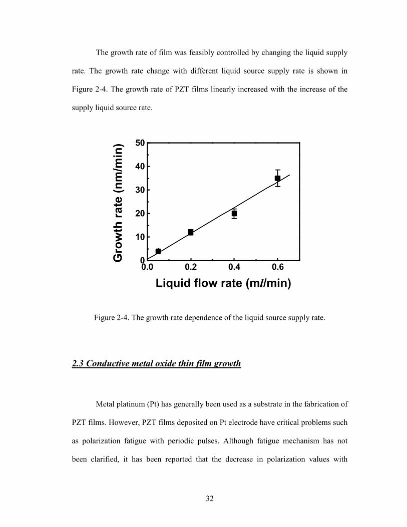
The growth rate of film was feasibly controlled by changing the liquid supply
rate. The growth rate change with different liquid source supply rate is shown in
Figure 2-4. The growth rate of PZT films linearly increased with the increase of the
supply liquid source rate.
0.0 0.2 0.4 0.60
10
20
30
40
50
Grow
thra
te(n
m/mi
n)
Liquid flow rate (ml/min)
Figure 2-4. The growth rate dependence of the liquid source supply rate.
2.3 Conductive metal oxide thin film growth
Metal platinum (Pt) has generally been used as a substrate in the fabrication of
PZT films. However, PZT films deposited on Pt electrode have critical problems such
as polarization fatigue with periodic pulses. Although fatigue mechanism has not
been clarified, it has been reported that the decrease in polarization values with

33
periodic pulses is related to domain pinning by the charged defects accumulated at
grain boundaries, domain boundaries and PZT/electrode interfaces. 53 , 54 Oxygen
vacancies that are mobile in PZT are the most probable charged defects. It has been
suggested that the Pt substrate must be replaced with conducting oxides such as RuO2,
IrO2, (LaXSr1-X)CoO3 and Sr0.5Ru0.5O3 to avoid the fatigue due to oxygen
vacancies.55,56,5758
Conductive metal oxide layers such as La0.5Sr0.5CoO3 (LSCO) and
Sr0.5Ru0.5O3 (SRO) were used as bottom electrode layers.
2.3.1 RF sputtering
For RF sputtering, a high-frequency generator is used generating
electromagnetic power in the MHz Region (typically 13.56 MHz). Therefore, the
sputtering target is alternatively bombarded by ions and then electrons to avoid
charge build-up which limits the use of dc-sputtering for insulating thin film
deposition.
Figure 2-5. RF sputtering configuration.

34
50 – 60 nm of LSCO or SRO electrode layers were deposited at room
temperature on SrTiO3 / Si or SrTiO3 substrates by RF sputtering with a power of 300
W for 30 min. A mixed gas with a ratio of 5 : 1 for Ar : O2 was used as the reactive
and the oxidation source.
The samples were then annealed at 600 – 650 oC for 1 hour in an oxygen-
flowing tube furnace to obtain an epitaxial buffer layer for PZT films. The cooling
rate was set to 5 oC/min after annealing.
2.3.2 Pulsed laser deposition (PLD)
PLD was used to prepare Sr0.5Ru0.5O3 thin films. In the PLD technique, a laser
beam (most frequently an excimer laser) is directed at a solid target. The interaction
of the pulsed laser beam with the target produces a plume of material that is
transported toward a heated substrate placed directly in the line of the plume.
50 - 60 nm thick SRO layers were prepared at 630 oC by pulsed laser
deposition (PLD) where KrF laser with a wavelength of 248 nm was used. The
deposition was carried out at 200 mTorr of oxygen for 30min and the samples were
cooled down from growth temperature in 1 atmosphere of oxygen to prevent the
occurrence of high oxygen vacancy concentration.
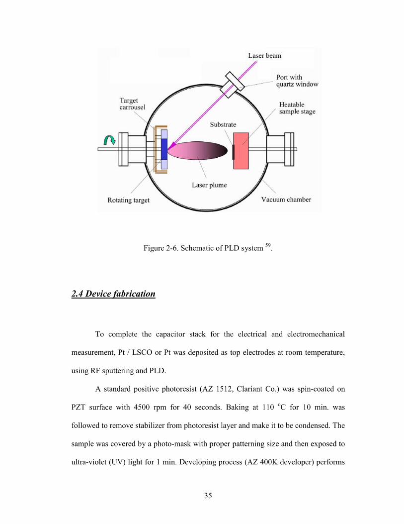
The schematic diagram of a PLD chamber is illustrated in Figure 2-6.
35
Figure 2-6. Schematic of PLD system 59.
2.4 Device fabrication
To complete the capacitor stack for the electrical and electromechanical
measurement, Pt / LSCO or Pt was deposited as top electrodes at room temperature,
using RF sputtering and PLD.
A standard positive photoresist (AZ 1512, Clariant Co.) was spin-coated on
PZT surface with 4500 rpm for 40 seconds. Baking at 110 oC for 10 min. was
followed to remove stabilizer from photoresist layer and make it to be condensed. The
sample was covered by a photo-mask with proper patterning size and then exposed to
ultra-violet (UV) light for 1 min. Developing process (AZ 400K developer) performs

36
photoresist removal by breaking down the structure of the exposed region and shapes
circular holes. Care must be taken to avoid overdeveloping or incomplete developing
which can be a critical factor to define the precise dimension and good contact
between electrode and PZT films.
This was followed by LSCO and Pt deposition at room temperature. The
standard lift-off was used to make discrete top electrodes. In lift-off process, samples
were dipped in acetone that dissolves underlying photoresist layer. The typical
thickness of Pt top electrodes was 60 - 80 nm. The circular electrode diameter was
between 18 and 50 µm. This process formed device structure for electrical
measurement.
The final sample structure is shown in Figure 2-7.
Figure2-7. Sample structure after device fabrication.
Substrate (STO or STO/Si)
Bottom electrode (LSCO or SRO)Ferroelectric layer (PZT or BFO)
Top electrodeBottom electrode
37
2.5 Characterization
2.5.1 X-ray Diffraction (XRD)
X-ray diffraction (XRD) is a powerful method, which is widely used for the
characterization of crystalline and structural properties with non-destructivity. When
monochromatic X-ray radiation is incident upon the sample, a part of the radiation is
scattered from the sample atoms. Scattered X-rays constructively interfere when
certain conditions are satisfied. This phenomenon is known as diffraction of X-rays.
Two incident rays are scattered from two atomic planes of the crystal. The traveling
difference of two rays is equal to the double product of the interatomic plane distance
dhkl and the sin function of the incident angle θ. If the traveling difference is equal to
an integer number of the incident X-ray wavelength then the constructive interference
of the diffracted beam occurs and a sharp diffraction peak can be observed.
This is expressed by Bragg’s Law [Eq. (2-1)];
θλ sin2dn = (2-1)
where n is an integer, λ is the wavelength of X-rays (generally, Cu Kα
(1.54056Å)), d is the lattice interatomic spacing and θ is the diffraction angle.
In the case of thin films, lattice mismatch between the grown film and the
substrate occurs, which is an important factor in thin film material properties as well

38
as epitaxial devices. Thus, the complete set of XRD experiments enables to determine
and compare the lattice parameters of the substrate and the grown films.
In this study, XRD measurements were carried out by Siemens D5000 four-
circle diffractometer with monochromatized Cu Kα radiation. A typical θ - 2θ scans,
ω - rocking curves and φ scans were performed in the XRD studies.
The XRD measurement techniques are schematically illustrated in Figure 2-8.
Figure 2-8. XRD measurement techniques.
2.5.2 Rutherford backscattering (RBS)
Rutherford backscattering (RBS) was employed for analyses of the
composition and thickness of films with various growth conditions. A 2.00 MeV
4He+ ion beam was directed at normal incidence to the sample surface and then
θθθθ θθθθ
φφφφ-scan
θθθθ −2−2−2−2θθθθ scan
ωωωω-scan
DetectorX-ray source
ωωωω

39
detected at a scattering angle of 168o. Channeling measurements were used to
evaluate the heteroepitaxial quality of PZT films.
Figure 2-9 shows a typical RBS result of a Pb(Zr0.2Ti0.8)O3 film. The
calculated minimum-channeling yield obtained from random spectrum and aligned
spectrum was 10 - 15 % from PZT films grown on STO substrate, which indicates an
excellent crystalline property of PZT films.
Figure 2-9. RBS result for a sample of PZT film on STO substrate.

40
2.5.3 Ferroelectric property characterization
The ferroelectric properties were characterized using a Radiant Technologies
(RT) 6000 ferroelectric test system which is available for measurements of charge
hysteresis, pulse response, bipolar resistivity, pulse polarization cycling vs. fatigue
cycling and retention loss vs. time.
Hysteresis polarization measurement
In Figure 2-10, the hysteresis drive profile is illustrated. The hysteresis
measurement is performed by applying two single triangle waves which have
opposite voltage. A triangle wave with the input positive voltage (+Vmax) is applied
first and the negative voltage (-Vmax) is followed. The measure charge values at each
step are plotted as polarization (Q/A = µC/cm2) vs. voltage.
Figure 2-10. Signal drive profile for hysteresis polarization measurement.

41
Pulse polarization measurement
The pulse sequence to extract the switching polarization, called PUND, is
shown in Figure 2-11. Switched and non-switched polarization is measured and
polarization induced by domain switching (∆P = P* - P^) can be determined. In ideal
case, the polarization measured from hysteresis loop measurement must be equal to
the switching polarization obtained from a pulse polarization (2Pr ≈ ∆P).
Figure 2-11. Sequence of voltage pulses.
First sample is poled with one direction by negative pulse and the polarization
state after poling is marked as 1. This polarization state (-Pr) is switched by following
two pulses with opposite bias. The switched polarization (P*) and non-switched
polarization (P^) is measured from these two pulses. Consequently, intrinsic switching
polarization can be obtained from the relation of ∆P = P* - P^.

42
By doing this measurement, non-ferroelectric switching polarization induced
mainly by defects can be distinguished from ferroelectric domain switching. The
sequence of pulse and corresponding polarization state are illustrated in Figure 2-12.
Figure 2-12. Switching (P*) and non-switching (P^) polarization.
2.5.4 Capacitance-Voltage measurement
An HP 4194 gain impedance analyzer (Hewlett-Packard) was used for
dielectric property measurement at room temperature.
A small signal with 50 - 100 mV amplitude and various oscillation signal
between 100 Hz and 100 kHz in frequency was applied to the test capacitors while a
dc-bias was swept with up (negative bias to positive bias) or down (positive bias to
negative bias) sweep direction. The small signal capacitance was recorded and the
dielectric constant was calculated from the parallel plate equation [Eq. (2-2)];

43
tAC rεε 0= (2-2)
where, C is the capacitance, ε0 is the permittivity of free space, εr is relative
dielectric constant of the ferroelectric layer, A is electrode area and t is thickness.
2.5.5 Piezoelectric force microscopy (PFM)
The piezoelectric measurements and the domain structure in thin film, i.e.,
quantitative piezoelectric coefficient (d33) and piezoresponse domain imaging, were
carried out using piezoelectric force microscopy (PFM). A commercial Digital
Instruments Nanoscope IIIA Multimode scanning probe microscope, equipped with
standard silicon tips coated with Pt/Ir alloy for electrical conduction is used. The
schematic experimental setup is shown in Figure 2-13.
PFM measurement is based on the detection of the local electromechanical
vibration of the ferroelectric sample induced by an external ac voltage. An external
voltage with a frequency ω was applied on the film surface through the tip, which
generates a sample surface vibration with the same frequency due to the converse
piezoelectric effect. The lock-in amplifier detects the modulated deflection signal
from the cantilever which oscillates together with the sample. During measurement,
the frequency of the applied voltage was much lower than the cantilever resonant
frequency in order to avoid mechanical resonance of the cantilever.

44
Figure 2-13. Schematic of the experimental setup for piezoelectric measurements.60
In piezoelectric imaging, the voltage is applied directly on the surface of
sample through the conducting tip, which is used as a movable top electrode. By
scanning along the sample surface, the domain configuration of the sample can be
mapped out. The typical force constant of these tips was 5 N/m and the apex radius
was approximately 20 nm. The contact force was estimated to be around 70 100 nN.
In a quantitative d33 measurement, the output signal from the photodiode was
calibrated using a quartz-coated with top and bottom Au electrodes (2.3 pm/V).
The voltage is applied on the capacitor through the tip to top electrode. This
not only makes a homogenous electric field under the electrode, but also prevents the
build up of electrostatic interaction between the cantilever and the sample. The
measurement frequency of 6.39 kHz was used. Each capacitor was driven at
particular dc voltage to study the field dependence.

45
Chapter 3: Pb(Zr0.5Ti0.5)O3 thin film growth on Si
3.1 Background
Lead zirconate titanate (PZT) ferroelectric thin films have been extensively
studied as candidates for use in nonvolatile ferroelectric random memories
(FeRAMs)61,62,63, field effect devices64,65, microelectromechanical systems (MEMS)66,
and pyroelectric sensors67. Efforts to integrate ferroelectric thin films with Si-CMOS
technology have been greatly increased to enable commercially viable, high-density,
nonvolatile ferroelectric memories and other devices. However, the polycrystalline
nature of the PZT layer that is typically deposited on platinum-coated silicon wafers
can lead to the suppression of ferroelectric and piezoelectric properties of the films.
To improve such properties, employing the appropriate substrate must be considered
to lower the strain introduced by the mismatch of the substrate and the ferroelectric as
well as to control the PZT orientation to the desired direction.
Up to date, there has been significant progress in the growth of epitaxial
oxides on semiconductors. 68 , 69 , 70 , 71 Of specific interest is the development of
epitaxial SrTiO3 (STO) on silicon for use as an alternative gate dielectric.72,73,74 By
using insulating STO layer as a template/barrier, the epitaxial growth of ferroelectric
layers by a sol-gel method has been recently demonstrated.75
The orientation of epitaxial STO layer on Si substrate is illustrated in Figure
3-1. The STO layer allows the growth of a highly textured/epitaxial film, ensuring

46
high polarization as well as uniform properties over large scales and small feature
sizes. Such an approach is especially important when the ferroelectric grain size is
commensurate with that of the lateral dimensions of the storage cell. This
combination of ferroelectric thin film into a bulk semiconductor devices raises
practical issues due to the properties of the ferroelectric thin film itself and to process
integration.
Figure 3-1. Growth of epitaxial STO films on Si substrate
In this chapter the structural and physical properties of LaSrCoO3 / Pb(ZrXTi1-
X)O3 / LaSrCoO3 (LSCO/PZT/LSCO) capacitors, which can provide a solution to the
polarization fatigue problem, will be presented. In this study the dependence of PZT
film composition with the precursor mixing ratio, growth temperature, and switching
properties of epitaxial Pb(Zr0.5Ti0.5)O3 capacitors are addressed.
Si : 5.43 Å
STO : 3.905 Å

47
3.2 Growth condition control
In order to fully control the MOCVD deposition process, the ratio of
Zr/(Zr+Ti) in Pb(ZrXTi1-X)O3 films as a function of the Zr and Ti precursor ratios
(V(Zr) / V(Ti)) was mapped out. In this study x ranged from 0.2 to 0.8 at a deposition
temperature of 650 oC. The dependence of PZT composition with various
temperatures at specific precursor ratios was also investigated. Figure 3–2 shows the
relationship of Zr/(Zr+Ti) atomic ratio in the PZT films measured by RBS versus
supply precursor source mixing ratios.
0.0 0.2 0.4 0.6 0.8 1.00.00
0.25
0.50
0.75
1.00
Zr/(Z
r+Ti)
atomi
crati
oinf
ilm
Solution mixing ratio (Zr/(Zr+Ti))
Figure 3-2. The relation of atomic percent of Pb, Zr and Ti of PZT films was
measured by RBS with precursor mixing ratio prepared at 650 oC and the same
volume ratio (V(Pb) / V(Zr) = 1 ) of Pb and Zr precursors was used during deposition
at 650 oC.

48
The volumetric ratio of Pb was fixed between 20 - 30 % to get a proper
stoichiometric composition of Pb/(Pb+Zr+Ti) (~ 0.5). Even though the entire range of
compositions (0<Zr/(Zr+Ti)<1) of PZT films were able to be obtained with proper
solution mixing ratios, non-ideal solution behavior was observed. Keijser et al.
experimentally determined a non-ideality factor for a conventional bubbler system
where each precursor was thermally controlled separately.76 Non-ideality factor (K)
can be obtained by the following Eq. (3-1),
g
g
xxKx
x−=− 11 (3-1)
where, x and xg denote Zr/(Zr+Ti) ratio in film and gas phase, respectively.
As an approximation, we assume xg can be directly replaced with xl (liquid
mixing ratio of Zr/(Zr+Ti)). The obtained K value was 2.6, which is higher than the
result of 1.49 reported by Keijser et al. While conventional bubbler systems deliver
each precursor separately, liquid delivery systems have only one hot vaporization cell
where mixtures of three different precursors are vaporized simultaneously and then
delivered to the chamber together. Since the three precursors have different thermal
properties, such as evaporation temperature and thermal volatility, volumetric
solution mixing ratio cannot be the same as the supply gas ratio of each component at
a fixed temperature which means that xl is not equivalent to xg and other calibration
factors must be added to Eq. (3-1) to compensate for different thermal volatility. Even
though the K’s for liquid and gas delivery are not physically equivalent, they are still

49
useful in describing the relative ease of composition control, independent of delivery
method. Despite the relatively high non-ideality factor, it was still possible to
reproducibly control film composition.
Figure 3-3 shows the variation of Pb concentration in the film with changing
supply mixing ratio at a substrate temperature of 650 oC. Pb concentration in the film
became saturated at a supply mixing ratio of 20 % (Pb/(Pb+Ti+Zr) = 0.5).
0 10 20 30 400.00
0.25
0.50
0.75 (III)(II)
(I)Substrate temperature : 650 oCVaporizer temperature : 190 oC
Pb/(P
b+Ti+
Zr)in
film
Mixing ratio [Pb/(Pb+Zr+Ti)] (%)
Figure 3-3. The variation of Pb atomic percent grown at 650 oC with different liquid
supply flow rate.
This behavior is consistent with the well-known Pb concentration self-
regulation mechanism.76,77,78 This self-regulation behavior can be explained by the

50
existence of an equilibrium state between adsorption to substrate surface and
desorption to gas phase. The higher vapor pressure of PbO compared with ZrO2 and
TiO2 allows it to be readily re-evaporated from substrate at high temperature.
Competitive reactions between adsorption and re-evaporation on the substrate results
in a plateau, which can be used as process window.
The ferroelectric properties of PZT films were significantly influenced by the
Pb stoichiometry composition as shown in Figure 3-4.
(a) Pb-excess composition (b) stoichiometric composition
Figure 3-4. The effect of Pb stoichiometry
on ferroelectric properties of PZT films.
(c) Pb-deficient composition
-3 -2 -1 0 1 2 3-6.0k-4.0k-2.0k
0.02.0k4.0k6.0k
Polar
izatio
n(µµ µµC
/cm2 )
Applied voltage (V)-25 -20 -15 -10 -5 0 5 10 15 20 25-60
-40-20
0204060
Polar
izatio
n(µµ µµC
/cm2 )
Applied voltage(V)
-2 -1 0 1 2-3-2-10123
Polar
izatio
n(µµ µµC
/cm2 )
Applied voltage (V)

51
No hysteresis behavior or balloon-like opened-hysteresis loops were observed
from samples which have more than 10 % Pb excess. Saturated hysteresis loops were
obtained from 18.5 % < Pbfilm < 21 % composition of PZT films which correspond to
7.5 % deficient and 5% excess from stoichiometric Pb composition. On the other
hand, dielectric linear response was measured from Pb deficient films.
The variation of composition of each element in film with growth temperature
was shown in Figure 3-5. Volumetric mixing ratio of liquid sources was 29 : 29 : 52
of Pb : Zr : Ti and vaporizer temperature was fixed at 190 oC.
450 500 550 600 65005
101520253035
PbZrTi
Atom
ic%
inFil
m
Growth temperature (oC)
Figure 3-5. Composition dependence on growth temperature.

52
It was observed that Pb in PZT films decreases with increase of growth
temperature because of highly volatile thermal property meanwhile Ti has a slight
increase in the PZT films. The content of Zr in PZT films increased below 550 oC and
then saturated. From this plot, it was found that the lowest temperature to get
stoichiometric composition (0.9 < Pb/(Zr+Ti) < 1.1) is about 550 oC and Pb atomic
ratio in films drastically increased at low temperature occurred (lower than 500 oC).
The XRD patterns of PZT films deposited at various temperatures are shown
in Figure 3-6. As expected from composition measurement, highly [00l] oriented PZT
films without any secondary phase were formed above growth temperature of 500 oC.
However, only PbO peak was observed from film deposited at 450 oC.
20 25 30 35 40 45 50
PZT(
001) PZ
T(00
2)
450oC
650oC
Inten
sity(
arb.
unit)
600oC550oC500oC
2θθθθ (degree)
Figure 3-6. θ - 2θ XRD patterns from films deposited at different temperature.

53
P-E hysteresis loops and switched polarization (∆P = P* - Pr (~ 2Pr)) were
measured from these films. The higher polarization values were obtained from films
grown at high temperature as shown in Figure 3-7, which results from the better
crystallinity with high process temperature within stoichiometric composition.
-6 -4 -2 0 2 4 6 8-40-30-20-10
010203040
500 oC550 oC600 oC625 oC650 oC
Polar
izatio
n(µµ µµC
/cm2 )
Applied voltage(V)
0 5 10 15 200
10
20
30
40
500 oC
550 oC
600 oC
625 oC
650 oC
Polar
izatio
n(µµ µµ C
/cm2 )
Applied voltage(V)
Figure 3-7. (a) P-E hysteresis loops and (b) Switched polarization (∆P = P* - Pr (~
2Pr)) from films deposited at different temperature.
Pure oxygen was used an as oxidation source for the PZT thin film growth.
The deposition of metal oxides can theoretically be achieved without an added
oxidant source because a metal-oxygen bond is already present in metal β-diketonate
complex. On the other hand, metalorganic precursors contain carbon element already,
which can be the critical factor of the leakage problem when it is incorporated into
the films. Therefore it is necessary to add oxygen gas to fully convert the hydro-
carbon in β-diketonates complex to CO2 and H2O. The dependence of the oxygen
flow rate on the PZT film growth is shown in Figure 3-8.

54
20 25 30 35 40 45 50101
102
103
Inten
sity(
arb.
unit)
2θθθθ20 25 30 35 40 45 50101
102
103
104
105
Inten
sity(
arb.
unit)
2θθθθ
(a) (b)
Figure 3-8. The dependence of oxygen flow rate on the film growth (a) O2 : 0 sccm
and (b) O2 : 300 sccm.
Perovskite PZT phase was not formed without oxygen supply while the
epitaxial films were obtained with minimum oxygen flow rate of 300 sccm. Oxygen
flow rate of 500 sccm which is the pressure of 0.9 torr in chamber was used as a
growth condition.
3.3 Structural and electrical properties of Pb(Zr0.5Ti0.5)O3 films
Pb(Zr0.5Ti0.5)O3 films were obtained with the solution mixing ratio of 20 : 20 :
60 from Pb : Zr : Ti. This composition is close to the morphotropic phase boundary
(MPB). This composition possesses a lower coercive field, and large d33, which is
strong candidate for nonvolatile memory and new microelectromechanical systems
(MEMS).

55
A typical θ - 2θ x-ray diffraction scan of LSCO/PZT/LSCO is shown in
Figure 3-9, indicating that the LSCO/PZT/LSCO heterostructure is highly [00l]
oriented without any secondary phase. The in-plane φ-scan around the (101) peak
shown in the inset in Fig. 3-9 further confirms that the films grow with the expected
four-fold symmetry. A c-axis lattice parameter of 4.08 Å was calculated from the
diffraction patterns.
20 25 30 35 40 45 5010
100
1k
10k
LSCO
(002)
PZT(
002)
PZT(
001)
LSCO
(001)
Inten
sity(
arb.
unit)
2θθθθ (degree)
Figure 3-9. A typical θ-2θ x-ray diffraction scan and φ-scan of LSCO/ PZT/LSCO
capacitors deposited on STO/Si at 650 oC.
The capacitors were subjected to a variety of stringent electrical tests to probe
their performance characteristics. The hysteresis loops of 230 nm thick PZT films
measured at 1 V, 3 V, and 5 V are shown in Figure 3-10. The measured resistivity
0 50 100 150 200 250 3000
1k
2k
3k
4k
Inten
sity(
arb.
unit)
Phi (degree)
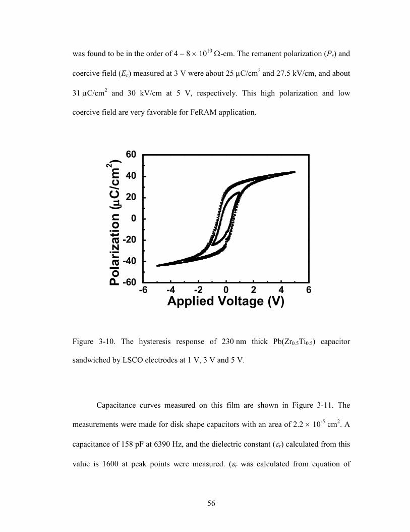
56
was found to be in the order of 4 – 8 × 10¹⁰ Ω-cm. The remanent polarization (Pr) and
coercive field (Ec) measured at 3 V were about 25 µC/cm2 and 27.5 kV/cm, and about
31 µC/cm2 and 30 kV/cm at 5 V, respectively. This high polarization and low
coercive field are very favorable for FeRAM application.
-6 -4 -2 0 2 4 6-60-40-20
0204060
Polar
izatio
n(µµ µµC
/cm2 )
Applied Voltage (V)
Figure 3-10. The hysteresis response of 230 nm thick Pb(Zr0.5Ti0.5) capacitor
sandwiched by LSCO electrodes at 1 V, 3 V and 5 V.
Capacitance curves measured on this film are shown in Figure 3-11. The
measurements were made for disk shape capacitors with an area of 2.2 × 10⁻⁵ cm2. A
capacitance of 158 pF at 6390 Hz, and the dielectric constant (εr) calculated from this
value is 1600 at peak points were measured. (εr was calculated from equation of

57
ACt
r ××=
0εε , where t is thickness, C is capacitance, ε0 is permittivity of free space and
A is electrode area). This value is close to the results obtained for films of similar
compositions and thicknesses grown by CVD.79
-8 -6 -4 -2 0 2 4 6 8
5.0x10⁻¹¹
1.0x10⁻¹⁰
1.5x10⁻¹⁰
2.0x10⁻¹⁰
Capa
citan
ce(F
)
Applied voltage (V)
Figure 3-11. Capacitance vs applied voltage measured with 230 nm thick
Pb(Zr0.5Ti0.5) capacitor sandwiched by LSCO electrodes.
In order to further characterize the capacitors, the pulsed polarization (∆P = P*
– P^) as a function of applied voltage is displayed in Figure 3-12.

58
0 2 4 6 8 10 12 140
10
20
30
40
50
Applied voltage(V)
Polar
izatio
n(µµ µµ C
/cm2 )
0
20
40
60
80
100Coercivefield(kV/cm)
Figure 3-12. Polarization (switched (P*) – non-switched (P^)) and coercive voltage
of LSCO/PZT/LSCO capacitors as a function of applied voltage.
It indicates a pulsed polarization value of 34 µC/cm2 and 36 µC/cm2
corresponding to 3 V and 5 V, respectively. In addition, the coercive field versus the
applied voltage is shown in the same figure. This figure shows that it saturates with
increasing the applied voltage; the coercive field is only 37.3 kV/cm (0.75 V) at 12
V, which is consistent with the properties of PZT near MPB 80 and ideal for low
voltage application.
Figure 3-13 shows the dependence of pulsed polarization (∆P) on pulse-width.
A key point of reference is the value of this pulse polarization at a pulse width of 1
µsec. The LSCO / PZT / LSCO capacitors show favorable pulse width dependence,
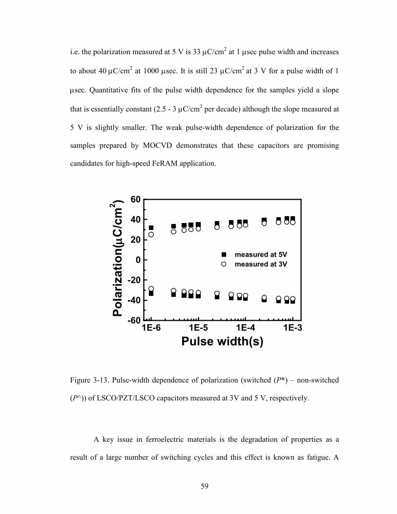
59
i.e. the polarization measured at 5 V is 33 µC/cm2 at 1 µsec pulse width and increases
to about 40 µC/cm2 at 1000 µsec. It is still 23 µC/cm2 at 3 V for a pulse width of 1
µsec. Quantitative fits of the pulse width dependence for the samples yield a slope
that is essentially constant (2.5 - 3 µC/cm2 per decade) although the slope measured at
5 V is slightly smaller. The weak pulse-width dependence of polarization for the
samples prepared by MOCVD demonstrates that these capacitors are promising
candidates for high-speed FeRAM application.
1E-6 1E-5 1E-4 1E-3-60-40-20
0204060
measured at 5Vmeasured at 3V
Polar
izatio
n(µµ µµC
/cm2 )
Pulse width(s)
Figure 3-13. Pulse-width dependence of polarization (switched (P*) – non-switched
(P^)) of LSCO/PZT/LSCO capacitors measured at 3V and 5 V, respectively.
A key issue in ferroelectric materials is the degradation of properties as a
result of a large number of switching cycles and this effect is known as fatigue. A

60
critical drawback in early ferroelectric memories was the fact that the total switched
charge decreased with use. Typically switched charge degraded to ~50 % of its initial
value after 106 writing/read cycles. This is crucial problem for ferroelectric memories
and fatigue in ferroelectric devices has been studied for many years. It has been
clearly demonstrated that the use of a conducting perovskite electrode (such as
LSCO) can eliminate polarization fatigue.81 Figure 3-14 shows the test capacitors
subjected to polarization fatigue testing via bipolar-pulsed cycles of both 3 V and 5 V
at 1 MHz. Fatigue characteristics of LSCO/PZT/LSCO capacitors measured at
different voltages shows no observable degradation up to 1011 cycles.
100 102 104 106 108 1010 1012-60-40-20
0204060
measured at 5 Vmeasured at 3 V
Polar
izatio
n(µµ µµC
/cm2 )
Cycles
Figure 3-14. Fatigue resistant characteristics of LSCO/PZT/LSCO capacitors as a
function of bipolar-pulsed cycles measured at 3 V and 5 V, respectively.

61
In order to confirm that the capacitors still retain a logic state (either ”1” or
“0”) after cycling, capacitors were subjected to the retention test. During a retention
test the decay in stored charge (polarization) of a capacitor which has already been
stored as a “1” or “0” logic state is measured as a function of time. The retention tests
were performed by applying a write pulse of 3 V and 5 V to a test capacitor, after a
specific period of time, and then applying two read pulses using the same voltage as
write voltage to measure the polarization. The difference of switched polarization (P*)
and nonswitched polarization (P^) is used to characterize the ability of retention to
distinguish the two logic states. Figure 3-15 shows desirable retention characteristics
measured at 3V and 5 V. The polarization of test capacitors did not decrease
apparently up to 105 sec.
100 101 102 103 104 10505
10152025303540
3V5VPo
lariza
tion(
µµ µµ C/cm
2 )
Time (sec.)
Figure 3-15. Retention characteristics of LSCO/PZT/LSCO capacitors as a function
of time measured at 3 V and 5 V, respectively.

62
PZT with composition around MPB is known to display anomalously high
dielectric and piezoelectric responses, which has also been observed in thin films.
Accordingly, PZT thick films have attracted a great deal of attention as actuators with
applications in MEMS devices.
The piezoelectric hysteresis loops for this MPB composition samples were
measured by using piezoresponse microscopy, which has been successfully used to
characterize piezoelectric properties of PZT capacitors.82, 83 Figure 3-16 shows the
piezoelectric hysteresis loops obtained from 230 nm- and 1, 3, 5 µm-thick
Pb(Zr0.5Ti0.5)O3 films. The obtained maximum out-of-plane piezoelectric coefficients,
i.e., d33, were 199, 208, 226 and 218 pm/V, respectively, which are higher than values
reported by other studies but still smaller than bulk value.
-400 -200 0 200 400-300-200-100
0100200300
235 nm1 µµµµm3 µµµµm5 µµµµm
d 33(p
m/V)
Applied electric field (kV/cm)
Figure 3-16. Piezoelectric hysteresis loops of 230 nm and 1, 3, 5 µm-thick
Pb(Zr0.5Ti0.5)O3 films.

63
Further analysis on d33 values of films compared to that of bulk will be
discussed in following section.
3.4 Comparison of piezoelectric properties of different thickness and
composition
As indicated in previous section, the PZT family of ceramics is widely used in
piezoelectric and dielectric applications. It was reported that compositions near the
morphotropic phase boundary (MPB) have the largest piezoelectric constants. 84
Especially, [001] oriented bulk PZT shows maximum values of 327 pm/V for the
tetragonal phase and above 500 pm/V for the rhombohedral phase. In this study, PZT
films with different thickness from 230 nm to 5 µm were fabricated and piezoelectric
properties were measured and compared with bulk values.
In order to avoid the complication induced by large discontinuity of d33
between tetragonal and rhombohedral structures, first we identified the structure of all
the samples. Careful measurements were performed by φ-scan and in plane lattice
parameter measurement. All the samples showed four-fold symmetry, which reveals
the cube-on-cube epitaxy, and tetragonal structure was confirmed by calculation of
c/a ratio (between 1.005 and 1.01). The obtained c/a values, which are smaller than
that of bulk (1.025), illustrates the in-plane tensile stress in PZT films induced by the
thermal mismatch between films and the Si substrate.
Figure 3-17 showed the variation of d33 values and coercive fields obtained
from 230 nm, 1 µm, 3 µm and 5 µm thick films. The obtained d33 values showed

64
almost constant values between 199 pm/V and 225 pm/V within experimental error,
while coercive field decreased sharply up to 1 µm and saturated at 10 kV/cm. In a
previous study, the effect of misfit on d33 was demonstrated, where the d33 of PZT
films on Si substrate were theoretically predicted. The obtained values in this study
agree well with the previously reported results.85
050
100150200250300350
d 33(p
m/V)
0 1 2 3 4 5 0102030405060 Coercivefield(kV/cm)
Film thickness (µµµµm)
Figure 3-17. The changes of piezoelectric coefficient (d33) and coercive field (Ec)
with film thickness; d33 of PZT films, Ec of PZT films
The compositional dependence of d33 on the Zr/(Zr+Ti) ratio has been further
investigated. All the samples were prepared with the thickness at 230±20 nm. Figure
3-18 demonstrates the relationship of experiment measured film d33 and the
theoretical bulk d33 (by Haun et al) with the composition of PZT films. 86 The
maximum d33, 199 pm/V, was obtained at MPB composition. This tendency is in

65
good agreement with those of bulk PZT. For reference, the dependences of d33 on the
Zr : Ti ratio obtained from PZT films grown by PLD and sol-gel are plotted in the
same figure.75,85 All the films were prepared on the same type of substrate
(LSCO/STO/Si). Although the experimentally measured values of d33 are still
significantly smaller than those theoretically predicted by Haun et al, PZT films
prepared by different growth methods show a similar values and trend.
0.2 0.3 0.4 0.5 0.6 0.7 0.80100200300400500600
d33 (bulk)MOCVDSol-gelPLD
d 33(p
m/V)
Ti/(Ti+Zr)
Figure 3-18. The changes of piezoelectric coefficient (d33) with change of Ti/(Zr+Ti)
ratio; -♦- d33 of bulk PZT calculated by Haun et al., d33 of thin PZT obtained from
MOCVD.

66
The values of remanent polarization (Pr) and saturation polarization (Ps) from
these hysteresis loops are plotted in Figure 3-19. For 0.27<x=[Ti/(Ti+Zr)]<0.55, Pr
values were in the range of 20–33 µC/cm2 and showed a clear dependence on x with a
minimum near the morphotropic boundary.
0.0 0.2 0.4 0.6 0.8 1.001020304050607080
Ps from Haun et al.MOCVD (Pr)MOCVD (Ps)PLD (Pr)PLD (Ps)Sputtering (Pr)
Polar
izatio
n(µµ µµC
/cm2 )
Ti/(Ti+Zr)
Figure 3-19. The variation of ferroelectric properties with change of Ti/(Zr+Ti) ratio;
-•- Ps of bulk PZT calculated by Haun et al., Pr from MOCVD, Ps from
MOCVD, ♦ Pr from PLD, ◊ Pr from PLD, and ο Pr from Sputtering.
The Pr values for rhombohedral compositions were measured along <001>
direction, but the polarization vector in these phases lies along the pseudocubic
<111> direction. Consequently, for rhombohedral compositions, only a projection of

67
the total polarization vector on the <001> was measured and actual values of Pr must
be higher than obtained values. The variation trend showed very similar to the
theoretical values by Haun et al. but still showed small values, which is attributed to
the thermal stress by the Si substrate and lattice mismatch strain between LSCO and
PZT layers. These effects will be discussed in next chapter.
3.5 Discussion
It should be mentioned that measured piezoelectric coefficients are still
smaller than theoretical value for bulk-PZT. This may be caused by several factors,
for example, the clamping from substrate, which can be reduced by creating sub-
micron islands of PZT capacitors (by Focused Ion Beam etching (FIB)). Accordingly,
d33 values close to theoretical prediction from FIB processed PZT capacitors have
been obtained where PZT films were prepared by pulsed laser deposition (PLD).85
These results suggest that d33 values are substantially suppressed in continuous films
by the clamping from the substrate.
The piezoelectric coefficient (d33) can be expressed as a function of
polarization (P), relative permittivity (ε33), and electrostrictive coefficient (Q)
according to the Eq. (3-2).87
PQd 3333 2 εεεε==== (3-2)

68
The suppression of d33 by the clamping from substrate can be expressed by the
Eq. (3-3).88
bEE
Ebf dSS
Sdd 311211
133333
2++++−−−−==== (3-3)
where, f and b denotes “film” and “bulk”, respectively, and Sij are elastic
compliances.
Considering the 50/50 composition films, bd31 = - 156 pm/v, bd33 = 327 pm/v (in tetragonal phase boundary),
ES13 = - 4.22×10⁻¹² m2/N, ES11 = 12.4×10⁻¹² m2/N, ES12 = - 4.06×10⁻¹² m2/N,86
then, fd33 (001)= 327 – 158 = 169 pm/v is expected from for single c-domains and
closed to experimentally observed values.

69
Chapter 4: Thickness effects in epitaxial Pb(Zr,Ti)O3 films
grown by MOCVD
4.1 Background
The stringent need for high-density, high-speed, and low-power memory
devices has prompted an immense interest in studying the size effect in ferroic
systems. However, a progressive degradation of ferroelectric properties has been
generally observed including the decrease of remnant polarization, the increase of
coercive field and a lower phase transition temperature with decreasing film
thickness.89,90,91 Consequently, the critical thickness of a ferroelectric thin film, i.e.,
the thickness limit when the ferroelectricity becomes unstable, has become an issue of
tremendous interest.
Based on the research performed during the last decade, several models have
been proposed to explain the size effect including both experimentally induced
imperfect film structures originating from deposition process, and theoretically
predicted intrinsic phenomena. The former describes the presence of a non-switching
and low-permittivity layer at the ferroelectric-electrode interface; meanwhile the
other comprises depletion, surface intrinsic effect and depolarizing effects. However,
both theoretical and experimental results have shown that critical thickness has been
changed with time.

70
Larsen et al. proposed blocking layer model where the presence of a non-
ferroelectric blocking layer in ferroelctric capacitors made with PZT films92. By
correcting for the influence of this layer, it was found that there is no thickness
dependence of ferroelectric properties, at least down to a thickness of 0.1 - 0.2 µm.
Meanwhile, Yanase et al. successfully reported sharp hysteresis loops and low
leakage in a 12 nm thick BaTiO3 film grown on SrRuO3 bottom electrodes, with a 2Pr
value of 65 µC/cm2.93 Moreover, the recent first principle calculations for a realistic
BaTiO3 thin films between two epitaxial metallic SrRuO3 electrodes under short
circuit conditions have shown that the critical thickness for ferroelectricity is of the
order of 6 unit cells which corresponds to 2.4 nm 94 where the reason for the
disappearance of a stable polar state was demonstrated to be a depolarizing
electrostatic field.
(a) (b)
Figure 4-1. (a) Evolution of the energy as a function of the soft-mode distortion ξ.
(b) Induced dipoles, potentials and depolarizing fields along the [001] direction of the
short-circuited ferroelectric capacitor. [Ref. 94]

71
In parallel, current nonvolatile memory manufacturing processes require a
scalable process such as metalorganic chemical vapor deposition (MOCVD) to grow
ferroelectric layers. Attempts to scale the operating voltage by reducing PZT
thickness are generally hampered by a substantial increase in coercive field (Ec) and a
marked decrease in switched polarization (Psw), particularly below 100 nm.
Accordingly, the research on thin film (tfilm<100 nm) growth by MOCVD has been
intensified to improve the properties and the understanding of size dependent
phenomena in thin films.
Physical vapor deposition (PVD) techniques, such as pulsed laser deposition
(PLD) and sputtering, have been employed to prepare samples for studying the size
effect in thin films because of the facile control of the stoichiometry.89,95,96 Only a few
quantitative studies on the properties of ultra-thin Pb(ZrxTi1-x)O3 (PZT) films grown
by MOCVD have been reported.90,97 However, quantitative results on the effects of
thickness scaling down to a few 10’s nm have been rarely reported because of the
complications in the chemical reaction and difficulties in controlling the growth
process in CVD. The experimental data, even for hundred of nanometers thick films,
have shown polarization values smaller than those predicted by theoretical
calculations. These findings have been explained by the presence of non-ferroelectric
interfacial layers and/or dislocations in films prepared by MOCVD.92,98 Up to date,
only a few films with intrinsic polarization values have been reported.99 In order to
investigate this size effect, preparing high quality films is the most important pre-
condition.

72
Another key aspect for reliable quantitative analysis of ultra-thin films is to
employ a suitable measurement technique. Traditionally, P-E hysteresis loop
measurements have been used to evaluate the ferroelectric properties in thin films.
However, polarization measurements for ultra-thin films are primarily dominated by
leakage and other methods are required.
A variety of techniques have been introduced to investigate ferroelectricity of
ultra thin film. Fong et al. observed ferroelectric phase of PbTiO3 on STO substrate
down to 3 unit cell thickness by observing the stripe domain formation with
synchrotron X-ray technique.100 Another example is that polarization dynamics in
ferroelectric films has been successfully studied at sub-micron scale with scanning
probe microscopy techniques. Notable examples are the works of Ahn et al. and
Tybell et al. in which the time dependence of local piezoelectric and electric field
signals suggests a stable ferroelectric polarization in PZT films down to thickness of
40 Å (10 unit cell).101 The advantage of the piezoelectric force microscopy (PFM)
technique is the reduced sensitivity to leakage currents, which is a major problem in
measuring ferroelectric properties for ultra-thin films. Previous research also has
shown that the polarization dynamics in ferroelectric films can be successfully
studied at submicron scale with scanning probe microscopy techniques.101,102,103
The approach in this study is based on two steps. First, epitaxial PZT films
with bulk-like properties were prepared, to enable the extraction of intrinsic
properties from extrinsic effects. Second, the thickness effect is investigated by
probing the local piezoelectric response by PFM.

73
4.2 Thickness effects in PZT thin films : a model system
Selecting suitable buffer layers between substrate and film can control the
strain in the film. In the case of capacitor devices, bottom electrode layers can play a
critical role as a buffer layer as well as conducting layer. Accordingly, the choice of
electrode materials must be considered for desirable electrical and crystalline
properties of PZT.
Figure 4-2. The lattice parameter constant variation with different composition of
zirconium to titanium in PZT. Lattice constants for electrodes (LSCO and SRO) are
also indicated.
PL
SRO
LSCOPS

74
Figure 4-2 demonstrates the lattice parameter constant variation with different
composition of zirconium to titanium in PZT. The key factor of this figure is to
compare the in-plane lattice constant misfit strain between PZT and electrodes. This
misfit strain can be expressed as Eq. (4-1).
PZTaelectrodeaPZTa
M−=ε (4-1)
Lattice mismatch between LSCO bottom electrode and Pb(Zr0.5Ti0.5)O3 is
pointed as PL, which is about 3.75 % misfit strain. On the other hand, SrRuO3, which
is also conductive metal oxide, can be outstanding candidate as a bottom electrode
layer because of its excellent lattice match with STO and Pb(Zr0.2Ti0.8)O3.
First, different thickness of Pb(Zr0.5Ti0.5)O3 films were prepared on
LSCO/STO substrates. SrTiO3 was selected as a substrate because the thermal
mismatch with PZT thin film is smaller than that with Si substrate. P-E hysteresis
loops and switching polarization (∆P) obtained from 20, 40, 70, 100 and 200 nm
thick Pb(Zr0.5Ti0.5)O3 films are shown in Figures 4-3(a) and (b). It was observed that
the decrease of polarization in the wide range of the thickness as film thickness
decreased and smaller polarization than theoretically expected intrinsic value was
obtained even with 200 nm thick films.

75
-400 -200 0 200 400 600-60-40-20
0204060
20 nm40 nm70 nm100 nm
Polar
izatio
n(µµ µµ C
/cm2 )
Applied electric field (kV/cm)
(a)
0 50 100 150 2000102030405060
Polar
izatio
n(µµ µµ C
/cm2 )
Film thickness (nm)0
50
100
150
200
d33 (pm/V)
(b)
Figure 4-3 (a) P-E hysteresis loops and (b) Switching polarization and d33 for 20, 40,
70, 100 and 200 nm thick Pb(Zr0.5Ti0.5)O3 films on LSCO/STO substrate.

76
In order to confirm the film quality, the thickness dependence of the
polarization and piezoelectric coefficient obtained from MOCVD-Pb(Zr0.5Ti0.5)O3
films was compared with the results obtained from Pb(Zr0.5Ti0.5)O3 films grown by
sputtering method (prepared by Prof. Eom group in Univ. of Wisconsin-Madison). As
shown in Figure 4-4, similar switching polarization (∆P) and d33 values and scaling
behaviors were obtained from Pb(Zr0.5Ti0.5)O3 films prepared by two different growth
methods. Both ∆P and d33 show the drastic decrease around 250 - 300 nm.
In epitaxial films and heterostructures, the strain due to lattice mismatch
between the film and the substrate can be relaxed by the formation of misfit
dislocations at the film-substrate interface. The relation between the critical thickness
for the formation of misfit dislocation and misfit strain can be described by the
Matthews-Blakesee model [Eq. (4-2)].
+
+= 1ln)1(8 b
chbch ενπ (4-2)
where, hc is the critical thickness for misfit dislocation formation, ν is the
Poisson’s ratio, b is the Burger’s vector, and ε is the lattice mismatch.
This misfit dislocation acts as an extrinsic dominating factors, such as
depolarizing field formation, in the scaling of polarization,104,105,106 which can be
significantly suppressed by selecting an optimum combination of substrate and PZT-
composition.

77
0 200 400 600 800 10000
20
40
60
80
LSCO/STO/SiLSCO/STOPo
lariza
tion(
µµ µµC/cm
2 )
Film thickness (nm)0 200 400 600 800 10000
50
100
150
200
250
LSCO/STO/SiLSCO/STO
d 33(p
m/V)
Film thickness (nm)
(a) (b)
0 200 400 600 800 10000
20
40
60
80
LSCO/STO/SiLSCO/STO
Polar
izatio
n(µµ µµC
/cm2 )
Thickness(nm)0 200 400 600 800 10000
50
100
150
200
250
Thickness(nm)
d 33(p
m/V)
LSCOSTO/SiLSCO/STO
(c) (d)
Figure 4-4 (a) ∆P vs film thickness (b) d33 vs film thickness from MOCVD-
Pb(Zr0.5Ti0.5)O3 films, (c) ∆P vs film thickness (d) d33 vs film thickness from
Sputtering-Pb(Zr0.5Ti0.5)O3 films.
As indicated in Figure 4-2, the approach of lattice engineering scheme to
investigate the thickness dependence was changed (from PL to PS).

78
As far as the composition of PZT films is concerned, we have focused on
Pb(Zr0.2Ti0.8)O3 with the conducting perovskite, SrRuO3 (SRO) [pseudocubic with
a=0.393 nm (calculated from the orthorhombic lattice parameters of a = 0.557, b =
0.553, and c = 0.785 nm)]. SRO is one of the most promising conductive metallic
oxides with very good thermal conductivity and stability, and high resistance to
chemical corrosion. Pb(Zr0.2Ti0.8)O3 thin films were prepared on SrRuO3(SRO) /
SrTiO3(STO) (001) substrates by liquid delivery MOCVD. SRO bottom electrode
with 50 - 60 nm thickness was deposited by pulsed laser deposition (PLD) at 630 oC
for 35 minutes.
AFM topographic images of the as-grown SRO bottom electrode surface
(Figure 4-5) showed that the surface is atomically flat terraces separated by single and
double atomic steps. Thus, these layers are applicable to the heteroepitaxial growth of
further oxide layers in applications requiring a conducting bottom layer.
The high surface quality (near-perfect) for under-layer is preliminarily
required to minimize leakage and surface roughness of PZT films.
For the quantitative electrical and electromechanical measurement, Pt was
deposited as the top electrode with 18-32 mm diameter circular pads patterned by
standard lift-off lithography processes.

79
Figure 4-5. AFM images of the SRO bottom electrode surface

80
4.3 The thickness effects in Pb(Zr0.2Ti0.8)O3 thin films
Prior to studying ultra thin films, we prepared and studied the ferroelectric
properties of relatively thick PZT films (~130 nm).
A typical θ - 2θ x-ray diffraction scan of PZT/SRO is shown in Figure 4-6 (a),
indicating that the PZT/SRO heterostructure is highly [00l] oriented without any
secondary phase. The in-plane φ-scan around the (101) peak shown in the inset in
Figure 4-6 (a) further confirms that the films grow with the expected cube on cube
four-fold symmetry. A c-axis lattice parameter of 4.14 Å was calculated from (002)
peak from the PZT diffraction patterns.
These films exhibited excellent crystalline property with ω - rocking full
width at half maximum (FWHM) of 0.26o and the minimum-channeling yield
(obtained from RBS) of 10 - 15 %.

81
20 25 30 35 40 45 50100
101
102
103
104
105
106
STO(
002)
SRO(
002)
PZT(
002)
Inten
sity(
a.u.)
2θθθθ-6 -4 -2 0 2 4 6-100
-75-50-25
0255075
100
Polar
izatio
n(µµ µµ C
/cm2 )
Applied voltage (V)
(a) (b)
1 2 3 4 5 6-200-150-100-50
050
100150200
∆∆∆∆P-∆∆∆∆P
Polar
izatio
n(µµ µµ C
/cm2 )
Applied voltage (V)-6 -4 -2 0 2 4 6
-60-40-20
0204060
d 33(p
m/V)
Applied voltage (V)
(c) (d)
Figure 4- 6(a) A typical θ - 2θ x-ray diffraction scan of 130 nm thick PZT/SRO/STO.
The in-plane φ-scan around the (101) peak shown in the inset. (b) P-E hysteresis
loops measured at a frequency of 16 kHz. (c) PUND (∆P = P* (switched polarization)
- P^ (non-switched polarization)) measurement. (d) Piezoelectric hysteresis loop
measured at room temperature.
0 50 100 150 200 250 3000
200
400
600
800
4
94
184
274
Inten
sity(
arb.
unit)
φφφφ (degree)
82
Sharp and square P-E hysteresis loops were obtained, with the remanent
polarization values (2Pr) of about 145 µC/cm2 as shown in Figure 4-6 (b), which
correspond to bulk-like ferroelectric properties.107 To extract the intrinsic polarization
switching, PUND (∆P = P*, i.e. switched polarization, - P^, i.e. non-switched
polarization) measurements were also performed and it was confirmed that obtained
values of 2Pr are consistent with the switched polarization, ∆P [Figure 4-6(c)].
The out-of-plane piezoelectric coefficient (d33) value of 60 – 65 pm/V
obtained from piezoelectric hysteresis loop is shown in Figure 4-6(d). The
experimentally obtained piezoelectric coefficient is in good agreement with
theoretical calculations for d33 of clamped PZT films.108,109
A set of hysteresis loops for 25, 34 and 130 nm thick films measured at a
frequency of 16 kHz is shown in Figure 4-7. The remanent polarization values (2Pr)
of 140 - 150 µC/cm2 were also observed with 25 and 34 nm thick films. Asymmetric
coercive fields were observed due to the asymmetric electrical boundary conditions
between the top (Pt/PZT) and bottom (PZT/ SRO) electrode interfaces. Small
openings were observed in the hysteresis loops of the 25 and 34 nm thick films which
are attributed to the leakage component effects in Pt top electrode side. The intrinsic
polarization switching was measured by pulse polarization measurement [PUND, ∆P
= P*, i.e. switched polarization, - P^, i.e. non-switched polarization] which is less
likely convoluted by leakage and nonlinear dielectric effects, and these polarization
values were confirmed.

83
-900 -600 -300 0 300 600 900-120-90-60-30
0306090
120 25 nm34 nm130 nm
Polar
izatio
n(µµ µµ C
/cm2 )
Electric field (kV/cm)
Figure 4-7. Ferroelectric hysteresis loops as a function of electric field for 25, 34 and
130 nm thick PZT films measured at 16 kHz.
Figure 4-8 shows piezoelectric hysteresis loops measured at room temperature.
Out-of-plane piezoelectric coefficient (d33) values of 55 – 65 pm/V in the thickness
range of 17 – 130 nm were obtained. For the 17 nm thick film, a saturated d33 (E)
hysteresis loop with 55 pm/V was observed, but unsaturated P-E polarization loops
due to high leakage current density were measured. This demonstrates that the
quantitative determination of d33 using an AFM setup is significantly less convoluted
by leakage, because the mechanical displacement of the cantilever is solely used for
this measurement. However, due to the large top electrode size, measurements on
films thinner than about 17 nm were mainly affected by leakage, and the results were
unreliable. P-E and d33-E hysteresis loops obtained from 17 nm thick film are shown
in Figure 4- 9.

84
-900 -600 -300 0 300 600 900-90-60-30
0306090
17 nm25 nm34 nm130 nm
d 33(p
m/V)
Electric field (kV/cm)
Figure 4-8. Piezoelectric coefficients, d33, loops as a function of electric field for 17,
25, 34 and 130 nm thick PZT films.
-900 -600 -300 0 300 600 900-75
-50
-25
0
25
50
75
Polar
izatio
n(µµ µµC
/cm2 )
Applied voltage (V)
-900 -600 -300 0 300 600 900-90-60-30
0306090
d 33(p
m/V)
Electric field (kV/cm)
(a) (b)
Figure 4-9 (a) Ferroelectric hysteresis loop and (b) piezoelectric coefficients, d33, loop
for 17 nm thick PZT film.

85
Therefore, local out-of-plane piezoelectric response measurements were
performed to study ferroelectricity in films thinner than 20 nm. The film thickness
was determined by cross section TEM images. Low magnification and high-
resolution cross-sectional TEM images of 34 nm thick PZT film are shown Figure 4-
10 (a) and (b).
(a)
(b)
Figure 4-10 (a) low magnification and (b) high resolution cross-section TEM images
of 34 nm thick PZT film.
STOSROPZT
60nm
SRO
PZT
2 nm

86
There was no second phase observed in TEM images and the epitaxial growth
with a sharp interface between PZT and SRO was confirmed. In addition, the 90o
domains are not observed with this thickness range.
Figures 4-11 (a), (b) and (c) show piezoelectric response images for the 34, 17,
and 8 nm thick films. First, the films were poled at a positive dc-bias by scanning
over an area of 1×1 µm2, followed by another poling at the opposite bias over a
0.5×0.5 µm2 area inside the previously poled area. The magnitude of the piezoelectric
response is defined as the peak-to-peak value of measured signal as shown in figures.
The obtained signal magnitudes were 863.4 mV for 34 nm, 562.5 mV for 17 nm and
357.1 mV for 8 nm thick films, respectively.
A clear piezoresponse image with a signal magnitude of 5.2 mV, which is
well above the noise level, was measured on a film as thin as 3.6 nm as shown in
Figure 4-12 (c). This image was obtained after a 1.5 V dc poling, by scanning with
the probe at an ac bias of 0.3 Vpp. From the high resolution TEM image in Figure 4-
12 (b), 8 - 10 unit cells of PZT films were counted.
This thickness is very close to the theoretically calculated critical thickness for
a BaTiO3 ferroelectric film by Junquera and Ghosez, where they predicted the critical
thickness for BaTiO3 thin films under short circuit conditions is 6 unit cells which
corresponds to 2.4 nm.94

87
(a)
(b)
(c)
Figure 4-11. Piezoelectric response images for (a) 34 nm (b) 17nm and (c) 8 nm thick
films. Piezoelectric response heights of 863.4 mV, 562.5 mV and 357.1 mV were
observed, respectively.

88
(a)
(b)
(c) (d)
Figure 4-12 (a), (b) Cross-section TEM images of 3.6 nm thick PZT film. (c)
Piezoelectric response images from 3.6 nm thick PZT films (8-10 unit cells). (d)
Piezoelectric response of 5.2 mV was observed with ± 1.5 V and 0.3 Vpp.
5.2 mV
15 nmPZT ==== 3.6 nmSRO
PZT
SRO

89
In contrast to polarization and d33, a drawback of the PFM technique is the
difficulty of making quantitative analyses because of the inherent variations in the tip
elastic constants, and also the uncertainties in electric field distribution at the tip apex.
In order to quantify the thickness dependent behavior, the measured
piezoelectric response signals were normalized to the value obtained from a 34 nm
thick film (863.4 mV) with same electric field. All the measurements were carefully
performed and confirmed by calibrating with the value obtained from 34 nm thick
films before and after measuring new samples. This is a reasonable approach because
the 34 nm thick films show almost the same polarization and converse piezoelectric
coefficient values as the 130 nm thick films which are considered bulk-like in terms
of the ferroelectric properties.
Figure 4-13 shows the dependence of ferroelectric order parameters
(switching polarization, and d33) on the film thickness, and the local piezoelectric
response. Polarization and d33 values were normalized with respect to the
theoretically expected values for substrate-clamped films.110
An abrupt drop of the normalized order parameters is observed between 10
nm and 20 nm thick films. Responsible for this decay can be imperfect film structures
grown during the deposition process, but theoretical calculations suggest that intrinsic
and extrinsic phenomena may produce the same effect.

90
0.1 1 10 1000.0
0.2
0.4
0.6
0.8
1.0PFM∆∆∆∆Pd33∆∆∆∆P - PLD filmsPZT(50/50)/LSCO
Norm
alize
dord
erpa
rame
ter
Film thickness (nm)
Figure 4-13. The behavior of ferroelectric order parameters in PZT films with film
thickness. Normalized amplitudes from PFM (), ∆P (∆) and d33 (∇) measurements
of Pb(Zr0.2Ti0.8)O3/SRO were plotted. The dash-line plot shows the experimental
result from PLD-PZT (Nagarajan et al.). The dependence of polarization (∆P) on
thickness in Pb(Zr0.5Ti0.5)O3/LSCO is also plotted in same scale.
Experimentally induced imperfections involve the presence of a non-
switching, and low-permittivity layer at the ferroelectric-electrode interface. As a
comparison, the results on thickness scaling of polarization in Pb(Zr0.5Ti0.5)O3 films
with a LaSrCoO3 (LSCO) bottom electrode are shown in the same figure. In this

91
system, the mismatch strain (PZT
LSCOPZTa
aa −=ε ) measured from XRD was 1.4 %,
which is almost one order of magnitude larger than the one measured for
Pb(Zr0.2Ti0.8)O3 on SRO (0.2 %). In the Pb(Zr0.5Ti0.5)O3/LaSrCoO3 system,
polarization does not saturate even at 250 nm thick films. As pointed out previous
section, this demonstrates that the formation of misfit dislocations or imperfect
interfacial layers due to large lattice mismatches or intermixing can induce a critical
degradation of ferroelectricity in thin films.
The theoretical models take into account depletion, intrinsic surface and
depolarizing effects, while a perfect structure is assumed. Recent results suggested
that the depolarizing field governs the suppression of ferroelectricity. A quantitative
study of the size effect was experimentally performed by Nagarajan et al.89 In this
study, a pulsed probing technique was used to measure the switching polarization of
PZT films grown by PLD and the size effect was scaled. It was suggested that the
depolarizing field governs the suppression of ferroelectricity as suggested by
Junquera and Ghosez.94 Those data are also plotted in Figure 4-13 for comparison,
and show a similar behavior to the piezoelectric response results obtained on
MOCVD-grown films.
Although the critical thickness observed from MOCVD-PZT films is almost same or
even smaller than that of PLD-PZT films, small shift to the thicker side was observed.
This small deviation in scaling behaviors between PLD-films and MOCVD-films
may originate from two main factors. First, the possible existence of error range or
sensitivity of different measurement techniques may give rise to the different values.

92
The other critical reason for this deviation may be induced by the film crystallinity or
composition change with thickness.
The surface chemical bonding state analysis on 4 and 17 nm thick PZT films
was performed by X-ray photoelectron spectroscopy (XPS). Typical XPS analysis
uses an incidence angle normal to the sample surface. However, it is necessary to
employ the low incidence angle (grazing incidence) to discern more clearly between
the surface and bulk states. XPS analysis was carried out with two different incidence
angle conditions. The high-resolution XPS results show no observable peak shift in
Pb, Ti, and Zr peaks for 4 and 17 nm thick films in both incidence angle conditions as
shown in Figure 4-14 (Pb 5d = 412.5 eV, Zr 3d5/2 = 180.4 and Zr 3d3/2 = 182.8, Ti
2p3/2 = 457.3 and Ti 2p1/2 = 463, O 1s = 528.9). However, it was found that the peak
widths of Zr peaks are wider for the 4 nm film compared to the 17 nm films, which is
more clearly observed in grazing incidence angle measurement. This demonstrates
that the Zr chemical bonding states influenced by chemical surrounding could be
different in 4 and 17 nm thick films and the broadening in a few top layers is more
pronounced. XPS work on PZT films by Vaidya et al. showed that the spin-orbit split
Zr 3d peak exhibits two binding states one at Zr 3d5/2 = 180.3 and Zr 3d3/2 = 182.7 eV
and the other at Zr 3d5/2 = 181.4 and Zr 3d3/2 = 183.8 eV. The lower bonding energy
doublet of the Zr 3d peak was assigned to Zr atoms present in the form of an oxide in
PZT, while the second Zr 3d doublet (Zr 3d5/2 = 181.4 and Zr 3d3/2 = 183.8 eV) is
shifted from the lower bonding energy doublet by about +1eV. It was suggested that
this species is consistent with a hydroxylated metal species, probably of the form
PbZrOx(OH)3-x.111

93
425 420 415 410 405 4000.0
0.2
0.4
0.6
0.8
1.0 Pb Peak Normal Incidence4 nm17 nm
Norm
alize
dInt
ensit
y
Binding Energy (EV)425 420 415 410 405 400
0.0
0.2
0.4
0.6
0.8
1.0 Pb peak Grazing Incidence4nm17nm
Norm
alize
dInt
ensit
y
Binding Energy (EV)
(a) (b)
188 186 184 182 180 178 176-0.20.00.20.40.60.81.0 Zr peak Normal Incidence
4 nm17 nm
Norm
alize
dInt
ensit
y
Binding Energy (EV)188 184 180 176-0.2
0.00.20.40.60.81.0 Zr peak Grazing Incidence
4 nm17 nm
Norm
alize
dInt
ensit
yBinding Energy (EV)
(c) (d)
465 460 4550.0
0.2
0.4
0.6
0.8
1.0 Ti Peak Normal Incidence4nm17nm
Norm
alize
dInt
ensit
y
Binding Energy (EV)465 460 455
0.0
0.2
0.4
0.6
0.8
1.0 Ti Peak Grazing Incidence4nm17nm
Norm
alize
dInt
ensit
y
Binding Energy (EV)
(e) (f)
534 532 530 528 5260.0
0.2
0.4
0.6
0.8
1.0
Surface adsorbedoxygen
Lattice oxygenof PZT
Norm
alize
dInt
ensit
y O peak Normal Incidence4nm17nm
Binding Energy (EV)534 532 530 528 526
0.0
0.2
0.4
0.6
0.8
1.0
Surface adsorbedOxygen
Lattice oxygenof PZT
O Peak Grazing Incidence4nm17nm
Norm
alize
dInt
ensit
y
Binding Energy (EV)
(g) (h) Figure 4-14. XPS analysis on 4 and 17 nm thick PZT films. Normal (a), (c), (e), (g)
and grazing incidence (b), (d), (f), (h) measurements. (a) and (b) : Pb (5d); (c) and
(d) : Zr (3d); (e) and (f) : Ti (2p); (g) and (h) : O (1s).

94
X-ray photoelectron spectrum obtained from Zr 3d in 4 nm thick film can be
interpreted by using this model. The precursor of Zr used in this study is
Tetrakis(dimethylheptanedionate)zirconium, [Zr(dmhd)4, (C9H15O2)4Zr], and the
hydroxide from this metalorganic source can be incorporated into PZT films when it
is not completely decomposed to form ZrO2. Accordingly, Zr spectrum measured
from 4 nm thick film is composed of two different chemical states as proposed in
Figure 4-15.
188 186 184 182 180 178 176-0.20.00.20.40.60.81.01.21.4
hydroxylatedmetal species[PbZrOx(OH)3-x]
Zr in the form ofoxide in PZT
4 nm17 nm
Norm
alize
dInt
ensit
y
Binding Energy (EV)
Figure 4-15. XPS spectrum of Zr 3d peak (Zr atoms present in the form of an oxide in
PZT and hydroxylated metal species, probably of the form PbZrOx(OH)3-x).

95
Contrary to the peak width changes in Zr, the same peak shape and width
from even for top layers were obtained from Pb. Now, the scaling behavior of
MOCVD-PZT films can be interpreted with XPS results. As discussed in previous
chapter, polarization and piezoelectric properties are the function of composition of
Zr to Ti while the stoichiometric composition for perovskite is governed by the
composition of Pb. This leads to the observation of piezoresponse in 4 nm thick films
but small deviation in scaling behavior with order parameters which was calibrated
with 34 nm thick Pb(Zr0.2Ti0.8)O3 films. This observation of clear difference of peak
widths in Zr was not found in PLD-PZT samples (it was insignificant even there
exists wider peak width in ~4 nm). However, further experiments to identify the
bonding states for these observations are needed.
4.4 Disccussion
In summary of this chapter, ultra-thin PZT films have been prepared by liquid
delivery MOCVD. The effect of reduced thickness on ferroelectricity in thin PZT
films was studied by comparing the magnitude of the piezoresponse signal as
measured by PFM with the quantitatively determined order parameters. It is found
that the films as thin as 8–10 unit cell thick PZT films shows a measurable
piezoelectric response.
It was found that the instability of surface chemical bonding state in ultra thin
films found in XPS results may affect the scaling behavior obtained from MOCVD-
PZT films. The formation of hydroxylated metal species is related to the activation

96
energy to form stable oxide phase and could be controlled by controlling the process
parameters. However, chemical reaction control to suppress hydroxylated metal
species is not clearly understood in this study. To carefully investigate chemistry and
reaction mechanism in PZT thin film process, an in-situ diagnostic method such as
FTIR or mass spectrometry can provide some more insights into the basic science of
CVD process. Clearly careful analysis is required to clarify these observations.

97
Chapter 5: BiFeO3 thin film growth by MOCVD
5.1 Background
There is currently significant interest in the field of ferroelectric thin film
materials and devices, with a strong focus on the integration of thin films on Si-
complementary metal-oxide semiconductor (CMOS) for non-volatile memory
(FeRAM) applications. Two ferroelectric perovskites, namely the lead zirconate
titanate (PZT) and strontium bismuth tantalite (SBT) family of materials have
emerged as the most attractive candidates for the storage capacitor layer. Although
considerable progress towards integration is being made, there are some key
questions that are pertinent to these materials systems. The optimum processing
temperatures are still quite high for the SBT system, although the recent progress in
reducing the temperature is very encouraging112, 113; in the case of the PZT system,
the inherent toxicity of lead is of great environmental concerns.
Therefore, it is quite desirable to have a ferroelectric material system that has
the large polarization properties and low temperature processability of the PZT
system with the chemical “benign-ness” of the SBT system.
In this regard, recently it has been reported that a significant ferroelectric
polarization was observed in epitaxial thin films of the lead-free perovskite, bismuth
ferrite (BFO) 114 , 115 , which was also observed by the studies of Yun and co-
workers 116 . A perovskite BFO has high Curie temperature (850 oC) 117 , 118 and

98
possesses a rhombohedrally distorted perovskite structure with space group
633 vCcR − in the bulk119. It has been reported that bulk BFO showed a polarization
of 3.5 µC/cm2 along (001) at 70 K, indicating a polarization of 6.1 µC/cm2 along
(111)120. The unit cell parameters of rhombohedral and pseudocubic are a = 5.616 Å,
and a = 3.96 Å, respectively.
It was found that bismuth ferrite could typically exist three different stable
phases, i.e., Bi25FeO40, BiFeO3, and Bi2Fe4O9, as shown in Bi2O3 - Fe2O3 phase
diagram (Figure 5-1) 121 . Therefore, careful analyses on the composition and the
crystal structure must be performed to identify the phase of samples.
Figure 5-1. Bi2O3 - Fe2O3 phase diagram.

99
In the process of exploring the viability of using this materials system as an
alternative ferroelectric system that embodies the positive attributes of both the PZT
and SBT systems into a FRAM memory process flow, it is imperative that a viable,
manufacturable process (such as a chemical vapor deposition) be available for the
deposition of the ferroelectric layer. In this chapter, the precursor chemistry, the
process window as well as the ferroelectric and piezoelectric properties of films
deposited on single crystal (001) SrTiO3 (STO) and STO / Si covered with an SrRuO3
(SRO) electrode layer will be described.
5.2 Growth conditions
An MOCVD equipped with liquid delivery system (LDS) was used with
Tris(2,2,6,6-tetramethyl-3,5-heptanedionate)bismuth (III) [Bi(thd)3] and Tris(2,2,6,6-
tetramethyl-3,5-heptanedionate)iron (III) [Fe(thd)3] dissolved in tetrahydrofuran
(THF) which are both based on β-diketonates as the liquid metalorganic precursor
materials. Their intrinsic similarity in organometallic chemistry makes them
reasonably compatible and the thermogravimetric (TG) curves of Bi(thd)3 and
Fe(thd)3 are shown in Figure 5-2. As indicated in TG analysis, Bi(thd)3 shows the
imperfect vaporization property leaving ~30 % residue even at 350 oC. The vaporizer
was clogged after about 5 hours of operation due to this residue.
An SRO layer was prepared by PLD at 650 oC as a bottom electrode and the
growth condition of MOCVD process is summarized in Table 5-1.

100
0 100 200 300 4000
20
40
60
80
100
Fe(thd)3Bi(thd)3
Weig
htlos
s(%)
Temperature (oC)
Figure 5-2. The thermogravimetric (TG) curves for Bi(thd)3 and Fe(thd)3.
precursors Bi(thd)3
Fe(thd)3
Vaporizer temperature 190 - 210 oC
Carrier gas flow rate 200 sccm
O2 gas flow rate 500 sccm
Substrate temperature 600 – 650 oC
Process pressure 2 Torr
Liquid solution flow rate 0.2 ml/min.
Table 5-1. Deposition parameters of BFO films prepared by liquid delivery MOCVD.

101
A showerhead that is designed to be heated with oil to avoid condensation of
vaporized precursors and achieves high uniform film deposition over a 2 in. substrate
was used.
Consistent with previous work on CVD process of PZT thin films, it was
found that the film composition and structure are quite sensitive to the substrate
temperature, the precursor delivery ratio as well as the vaporizer temperature122. The
variation of film composition with different precursor supply ratios is shown in
Figure 5-3.
0 10 20 30 40 50 60 70 80 901020304050607080
(III)(II)
Bi/(Bi+Fe)Pb/(Pb+Zr+Ti)
Bi/(B
i+Fe)
orPb
/(Pb+
Zr+T
i)inf
ilm(%
)
Bi or Pb solution mixing ratio (%)
(I)
Figure 5-3. Relation between Bi and Fe atomic percentage in BiFeO3 films as
measured by Rutherford backscattering (RBS) and energy disperse spectrometry
(EDS), for precursor mixing ratio prepared at growth temperature of 650 oC. Atomic
percentage ratio in Pb(ZrxTi1-x)O3 is also plotted at the same scale for comparison.
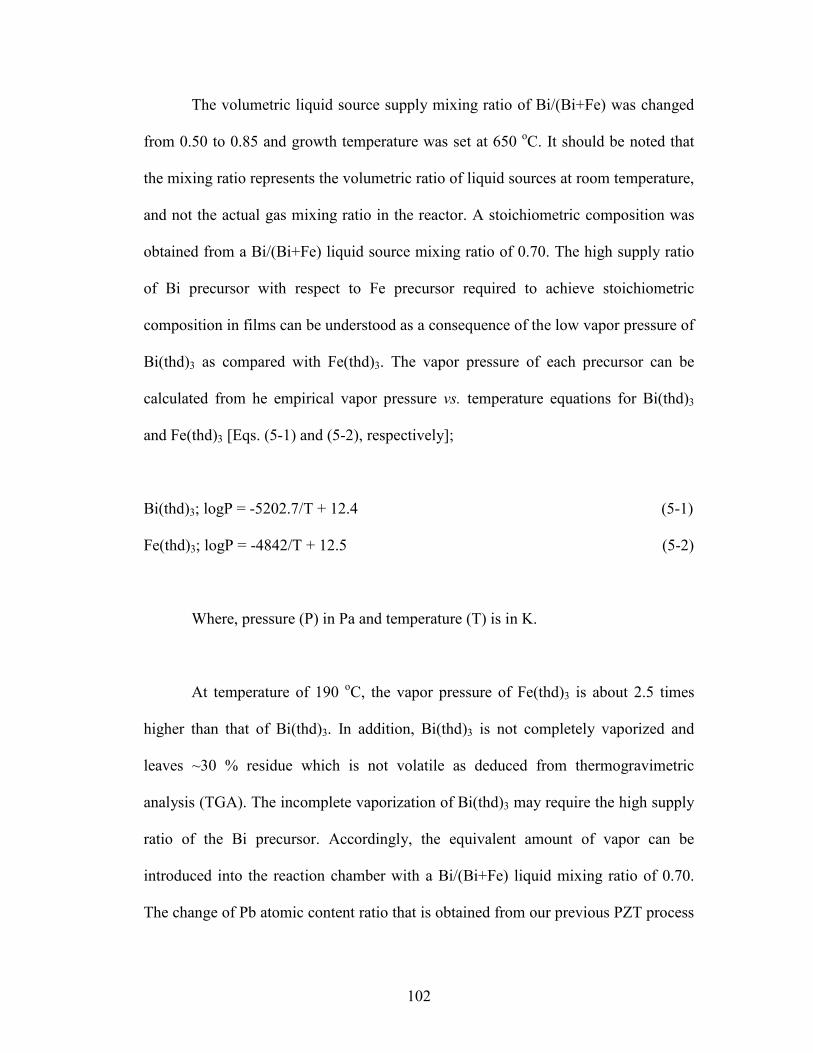
102
The volumetric liquid source supply mixing ratio of Bi/(Bi+Fe) was changed
from 0.50 to 0.85 and growth temperature was set at 650 oC. It should be noted that
the mixing ratio represents the volumetric ratio of liquid sources at room temperature,
and not the actual gas mixing ratio in the reactor. A stoichiometric composition was
obtained from a Bi/(Bi+Fe) liquid source mixing ratio of 0.70. The high supply ratio
of Bi precursor with respect to Fe precursor required to achieve stoichiometric
composition in films can be understood as a consequence of the low vapor pressure of
Bi(thd)3 as compared with Fe(thd)3. The vapor pressure of each precursor can be
calculated from he empirical vapor pressure vs. temperature equations for Bi(thd)3
and Fe(thd)3 [Eqs. (5-1) and (5-2), respectively];
Bi(thd)3; logP = -5202.7/T + 12.4 (5-1)
Fe(thd)3; logP = -4842/T + 12.5 (5-2)
Where, pressure (P) in Pa and temperature (T) is in K.
At temperature of 190 oC, the vapor pressure of Fe(thd)3 is about 2.5 times
higher than that of Bi(thd)3. In addition, Bi(thd)3 is not completely vaporized and
leaves ~30 % residue which is not volatile as deduced from thermogravimetric
analysis (TGA). The incomplete vaporization of Bi(thd)3 may require the high supply
ratio of the Bi precursor. Accordingly, the equivalent amount of vapor can be
introduced into the reaction chamber with a Bi/(Bi+Fe) liquid mixing ratio of 0.70.
The change of Pb atomic content ratio that is obtained from our previous PZT process

103
performed at the same growth temperature (650 oC) is also plotted in Figure 5-3122.
Here, it should be noted that the growth-window of BFO films appears to be much
smaller than that of PZT as can be seen in Figure 5-3. The composition change in the
Bi/(Bi+Fe) ratio shows an almost linear behavior with the liquid source mixing ratio,
while there is a relatively wide plateau region for the PZT film growth process. This
is generally explained by a “Pb self-regulating” mechanism at high temperature
growth processes and is used as the growth window123, 124 as discussed in previous
chapter.
5.3 Crystal structure
Crystal structures for different composition films were determined by a typical
θ - 2θ x-ray diffraction scan. Only (00l) diffraction peaks from BFO, SRO and STO
without any second phase were observed for films with the stoichiometric
composition [Figure 5-4 (designated as (II))].
The out-of plane lattice parameter calculated from the (002) peak of a 150 nm
thick BFO film is 4.03 Å. This value is larger than bulk lattice constant (3.96 Å)
because of the in-plane compressive strain induced by the substrate (SRO/STO).
However, additional secondary phase peaks such as (024) α-Fe2O3 (Rhombohedral,
cR3 , a = 5.112 Å, c = 13.82 Å) or (002) and (220) β-Bi2O3 (tetragonal, cP 124 , a =
7.741 Å, c = 5.634 Å) were observed in Fe- and Bi-rich films (designated as (I) and
(III), respectively) in Figure 5-4.

104
2 0 2 5 3 0 3 5 4 0 4 5 5 01 0 0
1 0 1
1 0 2
1 0 3
1 0 4
1 0 5
1 0 6
* αα αα-Fe 2O 3
αα αα-Fe 2O 3
Inten
sity(
arb.
unit)
2 θθθθ ( d e g r e e )
( I )*
2 0 2 5 3 0 3 5 4 0 4 5 5 01 0 0
1 0 1
1 0 2
1 0 3
1 0 4
1 0 5
1 0 6
( I I )
Inten
sity(
arb.
unit)
2 θθθθ ( d e g r e e )
* *
2 0 2 5 3 0 3 5 4 0 4 5 5 01 0 0
1 0 1
1 0 2
1 0 3
1 0 4
1 0 5
1 0 6
( I I I )
ββ ββ-Bi 2O 3
Inten
sity(
arb.
unit)
2 θθθθ ( d e g r e e )
**
Figure 5-4. θ - 2θ X-ray diffraction scans for (I) Fe-rich phase, (II) stoichiometric
composition and (III) Bi-rich phase. * : BiFeO3; •••• : SrRuO3; : SrTiO3.

105
The interface between SRO and BFO, observed in the cross-sectional high-
resolution transmission electron microscopy (HR-TEM) image as shown in Figure 5-
5, is atomically sharp and coherent.
Figure 5-5. Cross-sectional HRTEM image of BFO/SRO interface.
5.4 Surface morphology and Electrical properties
Subsequent to the optimization of the Bi:Fe ratio in the precursors, it was
proceeded to grow epitaxial films on single crystalline (001) STO and (001) STO / Si.
To facilitate heteroepitaxy and to introduce a conducting perovskite bottom electrode,
a 70 nm thick, epitaxial SRO layer deposited by pulsed laser deposition (PLD) was
used. For the electrical and electromechanical measurements, circular platinum (Pt)

106
pads with 32 µm diameter were deposited as top electrodes by a standard lift-off
process.
The surface morphologies of BFO films for different compositions measured
by atomic force microscopy (AFM) are shown in Figures 5-6 (a), (b) and (c). Out-of-
plane piezoelectric response measurements using piezoelectric force microscopy
(PFM) were performed to study the piezoelectric properties of these films, and the
results are shown in Figures 5-6 (d), (e) and (f).
The films were first poled at a negative dc-bias (-8 V) applied to a conducting
probe while scanning over a 2×2 µm2 area. In the case of stoichiometric films [figure
5-6 (e)], another poling was performed, with the probe biased at the opposite voltage
(+8 V) during scanning over a 1×1 µm2 area inside the previously poled area. Details
on the PFM technique can be found elsewhere125, 126.
A flat surface with 2 nm of peak-to-peak height was observed within the area
of 3×3 µm2 on 250 nm thick film with stoichiometric composition as shown in Figure
5-6 (b). A sharp piezoelectric response with complete reversible switching was also
observed as shown in Figure 5-6 (e). In the case of Fe-rich films, a rough, granular
surface was observed [Figure 5-6 (a)] and no piezoresponse was detected [Figure 5-6
(d)]. On the other hand, Bi2O3 islands were formed on a BFO matrix in the case of Bi-
rich films as shown in Figures 5-6 (c) and (f).
107
(a) Fe-rich (d) Fe-rich
(b) stoichiometric BiFeO3 (e) stoichiometric BiFeO3
(c) Bi-rich (f) Bi-rich
Figure 5-6. Surface morphologies (a), (b), (c) and out-of-plane piezoelectric response
measurements (d), (e), (f) using a piezoelectric force microscopy (PFM). The
thickness of films is ~250 nm.
0.0 0.3 0.6 0.9 1.2 1.5-3-2-10123
Heigh
t(nm
)
Scan distance (µµµµm)
108
An out-of-plane piezoelectric coefficient, d33, of 50 – 60 pm/V was measured
at room temperature, as shown in Figure 5-7 (a). The polarization-electric field (P-E)
hysteresis loops measured at 16 kHz on the 250 nm thick BFO film are shown in
Figure 5-7 (b). The sharp and square loops yield a 2Pr value of 110 - 120 µC/cm2.
This value is comparable to the theoretically predicted and experimentally obtained
values from PLD-grown films114, 127.
In order to extract the real switched polarization properties, PUND
measurements (∆P = P* (switched polarization) - P^ (non-switched polarization))
were also performed to confirm these values and the result is shown in Figure 5-7 (c).
The obtained switched polarization (∆P) is 110 - 120 µC/cm2 which is consistent with
the 2Pr value from the P-E hysteresis loop.
The electric field dependence of polarization with the results obtained for
BFO films grown by PLD and sputtering125 were compared. These three films
prepared by different growth methods showed very similar behavior. In all the cases,
switched polarization values of ~120 µC/cm2 were observed, which began to saturate
at 400 – 450 kV/cm. Moreover, the polarization showed weak pulse width
dependence in the range of 1 µsec - 1 msec, as shown in Figure 5-7 (d). This
demonstrates that the measured polarization switching is an intrinsic property of BFO
films, and is not dominated by leakage, which was a critical obstacle in determining
the ferroelectric property of bulk BFO120.

109
-600 -400 -200 0 200 400 600-60-40-20
0204060
d 33(p
m/V)
Electric field (kV/cm)
-600 -400 -200 0 200 400 600-80-60-40-20
020406080
Polar
izatio
n(µµ µµC
/cm2 )
Electric field (kV/cm)
(a) (b)
0 200 400 600 800 10000
306090
120150
BFO by CVDBFO by SputteringBFO by PLD
Polar
izatio
n(µµ µµC
/cm2 )
Electric field (kV/cm)
10-6 10-5 10-4 10-3-200-150-100-50
050
100150200
+ ∆∆∆∆P- ∆∆∆∆P
Polar
izatio
n(µµ µµC
/cm2 )
Pulse width (sec)
(c) (d)
Figure 5-7 (a) Piezoelectric coefficients, d33, loop as a function of applied voltage
from 250 nm thick BFO film. (b) P-E hysteresis loops as a function of applied voltage
from 250 nm thick BFO film measured at frequency of 20 kHz. (c) Pulsed
polarization (∆P) as a function of applied voltage at frequency of 20 kHz. (d) Pulse-
width dependence of switched polarization (∆P) in the range from 1µsec. to 1 msec.
at 15 V.

110
BFO films were also prepared on (001) Si using a 20 nm thick STO layer as a
template, and their properties were compared with those of films grown on STO
substrates.
Figure 5-8 shows P-E loops of BFO films grown on such substrates.
Polarization values (∆P) of 85 – 90 µC/cm2 and coercive fields of ~ 225 kV/cm were
measured for BFO films grown on Si substrate. These values are smaller than those
obtained for BFO films grown on STO, due to the in-plane tensile stress induced by
large thermal mismatch with silicon115. Out-of-plane lattice constants of 4 Å and 3.96
Å were observed for BFO films (200 nm) grown on STO and Si substrates,
respectively.
-600 -300 0 300 600 900 12001500-90-60-30
0306090
STO/SiSTO
Polar
izatio
n(µµ µµC
/cm2 )
Electric field (kV/cm)
Figure 5-8. P-E hysteresis loops obtained from BFO films on SRO / STO and SRO /
STO / Si substrates. XRD patterns around (002) BFO peaks are shown in inset.
43 44 45 46 47 48 49
*
BFO/SRO/STO/Si
BFO/SRO/STO
Inten
sity(
arb.
unit)
2θθθθ (degree)
*

111
5.5 Discussion
It has been demonstrated that a viable chemical vapor deposition process
enables the growth of high quality BiFeO3 thin films in this chapter. The
implementation of such a process into the potential FeRAM technology requires the
solution for some key issues.
First, the leakage current must be lowered by at least an order of magnitude.
This requires a careful study of the defect chemistry of the films as a function of Bi-
Fe ratio as well as other process parameters such as the substrate temperature and
oxygen ambient during cooling.
Second, the coercive field must be reduced to ~ 50 kV/cm (e.g., 1 V for a 200
nm thick film). Ferroelectric properties of BFO and PZT films are shown in Figure 5-
9. These figures clearly show the direction of the future study. Even though BFO film
shows the comparable polarization value, it has about 2-3 times higher coercive field
than that of PZT (20 / 80) film.
Lowering the coercive field of BFO film is a key question needs to be solved
for the realization of device applications. Careful studies of the switching
mechanisms in these films (180o versus 71/109o switching, and the interplay between
ferroelectric and ferroelastic switching125, 128) are needed.

112
-600 -400 -200 0 200 400 600-100-75-50-25
0255075
100Pb(Zr0.2Ti0.8)O3BiFeO3
Polar
izatio
n(µµ µµC
/cm2 )
Electric field (kV/cm)
(a)
0 2 4 6 8 10 120
306090
120150180
Pb(Zr0.2Ti0.8)O3BiFeO3Po
lariza
tion(
µµ µµC/cm
2 )
Applied voltage (V)
(b)
Figure 5-9. Comparison of (a) P-E hysteresis loops and (b) coercive fields
dependence obtained from BFO and PZT films on SRO / STO.

113
Third, the growth temperature must be reduced. Preliminary studies indicate
that this should be possible, in agreement with the reports of Yun et al.116. From the
CVD chemistry point of view, it is critical to explore the processing space to identify
the possibility of a “self-regulating” reaction zone. In this regard, preliminary results
show that a post-deposition oxygen flush of the film surface appear to hold promise in
terms of removing the excess Bi on the surface.

114
Chapter 6: Summary and future work
In this dissertation, a systematic study of the process controls as well as the
ferroelectric and piezoelectric properties of two ferroelectric material systems, lead
zirconate titanate (PZT) and bismuth ferrite (BFO), prepared by MOCVD has been
carried out. In order to feasibly control the precursor partial pressure and flow rate a
liquid delivery system (LDS) was equipped to MOCVD chamber. Precursors based
on β-diketonate were used for thin film growth and the characteristics of deposited
films showed crucial dependence on deposition temperature, deposition environment,
and kinetic factors such as the precursor partial pressure and flow rate.
In PZT system, the changes of spontaneous polarization (Ps) and piezoelectric
coefficient (d33) with Ti/(Zr+Ti) ratio are presented and compared with theoretical
values. Ferroelectric and piezoelectric properties at the composition close to
morphotropic phase boundary (MPB) region (Pb(Zr0.5Ti0.5)O3) have been investigated
for application in nonvolatile ferroelectric random access memories (FeRAM) and
microelectromechanical system (MEMS). These capacitors show desirable
ferroelectric properties such as high polarization and small coercive field, which
proves that this approach is very promising for both fundamental study and potential
applications.
The scaling of ferroelectric properties with film thickness in Pb(Zr0.2Ti0.8)O3
films grown on SrRuO3/SrTiO3(001) was studied. The PZT films are single
crystalline, c-oriented, and showed bulk-like properties for thickness above ~20nm.
Piezoelectric force microscopy (PFM) was employed to investigate the ferroelectric

115
properties of films thinner than 20 nm. Piezoelectric response was observed down to a
film thickness of 8 – 10 unit cells. A quantitative analysis of the size effect in
Pb(Zr0.2Ti0.8)O3 films was performed using the piezoelectric response. From the high
resolution XPS analysis, it was found that a hydroxylated metal species were formed
on a top few layers. This imperfect chemical state induced by unstable chemical
reaction in MOCVD process can be the main factor for the deviation in determining
the ferroelectric scaling in ultra thin films (thinner than 10 unit-cells).
Epitaxial BiFeO3 thin films were grown by MOCVD using Bi(thd)3 and
Fe(thd)3 as precursors. This research was the first challenge to prepare this material
system by MOCVD process. A systematic study on deposition process control such
as stoichiometric composition, structure change and growth temperature was carried
out. The film composition and phase equilibrium are sensitive to the Bi:Fe ratio in the
precursor. In the optimized growth condition which is very small growth window,
high quality epitaxial single perovskite phase thin films were obtained. Electrical
measurements using both quasi-static hysteresis and pulsed polarization
measurements confirm the existence of ferroelectricity with a switched polarization of
110-120 µC/cm2, ∆P (= P* - P^). Out-of plane piezoelectric (d33) measurements using
an atomic force microscope yield a value of 50 – 55 pm/V. These values are
comparable to the theoretically predicted and experimentally obtained values from
PLD-grown films.

116
Further research will be performed on both material systems (PZT and BFO)
which has not been completely understood in this study.
1) A careful quantitative analysis of the effect of hydroxylated metal species
on the thickness effect on the ferroelectric properties can extract the real thickness
effect of PZT films prepared by MOCVD. This study needs precise computing
simulation of XPS results and careful analysis on the structure in ultra thin films.
2) A perovskite BiFeO3 system could be a promising alternative ferroelectric
material for the current most popular PZT system due to its large ferroelectric
polarization and environmentally favorable nature. This makes it an interesting
replacement candidate for Pb-based ferro/piezoelectrics. However, BiFeO3 has about
3 times higher coercive field than that of PZT film and lowering the coercive field of
BiFeO3 film is a key question needs to be solved for the realization of device
applications as discussed in Chapter 5. One of the possible approaches is by doping
BiFeO3 with other elements, e.g. lanthanum.129,130,131 This design is inspired from
lowering the Curie temperature or tailoring the domain switching mechanism by
doping with lanthanum. 132 The spontaneous polarization and coercive field are
expected to be lowered by reducing the distortion of the structure.
3) As indicated in Chapter 5, the growth window for BiFeO3 film is very
small in MOCVD process and secondary phase is prone to form which is also
applicable in pulsed laser deposition.133 A relatively wide “self-regulating” growth
window with stoichiometric composition is very attractive aspect in the growth
process. This can lead to the availability of large-scale wafer process and greater
process flexibility. In order to verify the existence of “self-regulating” growth

117
mechanism in BiFeO3 system, the following directions can be considered for further
research.
i) The effect of growth temperature.
ii) The effect of oxygen partial pressure.
iii) Growth process control such as cooling rate and cooling in oxygen
atmosphere.

118
REFERENCES 1 J. Valasek, Phys. Rev. 15 (6), 537 (1920); 17 (4), 475 (1921). 2 D. W. Chapman, J. Appl. Phys. 40, 2381 (1969). 3 R. B. Atkin, Ferroelectrics 3, 213 (1972). 4 M. Francombe, Ferroelectrics 3, 199 (1972). 5 P. M. Heyman and G. H. Heilmeier, Proc. IEEE 54, 842 (1966). 6 S. Mathews, R. Ramesh, T. Venkatesan, J. Benedetto, Science 276, 238 (1997). 7 J. F. Scott and C. A. Paz de Arauzo, Science 246, 1400 (1989). 8 A. Mannish, Ferroelectrics 102, 69 (1990). 9 B. Jaffe, W. R. Cook, and H. Jaffe, “Piezoelectric Ceramics”, Academic Press
(1971). 10 M. E. Linesand A. M. Glass, Priciples and applications of Ferroelectrics and
Related Materials (Oxford University Press, Oxford, 1997). 11 M. J. Haun, E. Furman, S. J. Jang, and L. E. Cross, Ferroelectrics 99, 45 (1989). 12 Fujitsu’s FRAM technology solution, “What’s new about FRAM”, 20 (2002). 13 A. Erbil, W. Braun, B. S. Kwak, B. J. Wilkens, L. A. Boatner and J. D. Budai, J.
Crystal Growth 124, 684 (1992). 14 D. L. Schulz and T. J. Marks, Adv. Mater., 6, 719 (1994). 15 Toshio Hirai and Hisanori Yamane, J. Crystal Growth 107, 683 (1991). 16 K. Endo, H. Yamasaki, S. Misawa, S. Yoshida, and K. Kajimura, Nature 355, 327
(1992). 17 Mikko Ritala, Kaupo Kukli, Antti Rahtu, Petri I. Raisanen, Markku Leskela, Timo
Sajavaara, Juhani Keinonen, Science 288, 319 (2000).

119
18 Anthony C. Jones, Chem. Vap. Deposition 4, 169 (1998). 19 Hiroshi Funakubo, Tsuyoshi Hioki, Masato Otsu, Kazuo Shinozaki and Nobuyasu
Mizutani Jpn. J. Appl. Phys. 32, 4175 (1993). 20 A. C. Jones, P. A. Williams, P. R. Chalker, S. Taylor, A. Zoolfakr, L. M. Smith, P.
McGraw, Integr. Ferroelectr. 57, 1271 (2003). 21 K. J. Hubbard and D. G. Schlom, J. Mater. Res. 11, 2757 (1996). 22T. Nakagawa, J. Yamaguchi, M. Okuyama and Y. Hamakawa, Jpn. J. Appl. Phys.
21, L655 (1982). 23 M. Okada, K. Tominaga, T. Araki, S. Katayama and T.Sakashita, Jpn. J. Appl.Phys.
29, 718 (1990). 24 Yukio Sakashita, Hideo Segawa, Kouji Tominaga, and Masaru Okada, J. Appl.
Phys. 76, 2405 (1994). 25 P. K. Larsen, G. J. M. Dormans, D. J. Taylor and P. J. Van Veldhoven, J. Appl.
Phys. 73, 7857 (1993). 26 M. De Keijser, J. F. M. Cillessen, R. B. F. Janssen, A. E. M. De Veirman and D. M.
de Leeuw, J. Appl. Phys. 79, 393 (1996). 27 C. M. Foster, G.-R. Bai, R. Csencsits, J. Vetrone, R. Jammy, L. A. Wills, E. Carr,
and Jun Amano, J. Appl. Phys. 81, 2349 (1997). 28 Hiroshi Funakubo,a) Masanori Aratani, Takahiro Oikawa, Kouji Tokita, and
Keisuke Saito, Appl. Phys. Lett. 92, 6768 (2002). 29 Hajime Nonomura, Hironori Fujisawa, Masaru Shimizu and Hirohiko Niu, Jpn. J.
Appl.Phys. 41, 6682 (2002).

120
30 Vladislav V. Krisyuk, Aciya E. Turgambaeva, and Igor K. Igumenov, Chem. Vap.
Deposition, 4. 43 (1998). 31 K. Nagashima, H. Funakubo, S. Seki, Y. Sawada, Y. Miura, N. Higuchi, and H.
Matchida, Chem. Vap. Deposition. 6, 311 (2000). 32 J. F. Roeder, T. H. Baum, S. M. Bilodeau, G. T. Stauf, C. Ragaglia, M. W. Russell,
and P. C. Van Buskirk, Adv. Mater. Opt. Electron. 10, 145 (2000). 33 H. K. Ryu, J. S. Heo, S. I. Cho, and S. H. Moon, J. Electrochem. Soc. 146, 1117
(1999). 34 R. Ramesh, S. Aggarwal, and O. Auciello, Materials Science and Engineering R,
32, 191 (2001). 35 D. L. Schultz, T. J. Marks, Adv. Mater. 6, 719 (1994). 36 T. J. Marks, Pure Appl. Chem. 67, 313, (1995). 37 Introduction to Solid State Physics, C. Kittel, (1976). 38 A. L. Roytburd, S. P. Alpay, V. Nagarajan, C. S. Ganpule, S. Aggarwal, E. D.
Williams, and R. Ramesh, Phys. Rev. Lett. 85, 190 (2000). 39 M. D. Glinchuk, E. A. Eliseev, and V. A. Stephanovich, Physica B 322, 356
(2002). 40 J. Junquera and P. Ghosez, Nature 422, 506 (2003). 41 I. P. Batra, P. Wurfel, and B. D. Silverman, J. Vac. Sci. Technol. 10, 687 (1973). 42 R. R. Mehta, B. D. Silverman, and J. T. Jacobs, J. Appl. Phys. 44, 3379 (1973). 43 Y. Sotome, J. Senjaki, S. Morita, S. Tanimoto, T. Hirai, T. Ueno, K. Kuroiwa, and
Y. Tarui, Jpn. J. Appl. Phys. 33, 4066 (1994). 44 T. Y. Kim, D. Kim, and C. W. Chung, Jpn. J. Appl. Phys. 36, 6494 (1997).

121
45 C. M. Foster, G.-R. Bai, R. Csencsits, J. Vetrone, R. Jammy, L. A. Wills, E. Carr,
and Jun Amano, J. Appl. Phys. 81, 2349 (1997). 46 H. Fujisawa, M. Yoshida, M. Shimizu and Hirohiko Niu, Jpn. J. Appl. Phys. 37,
5132 (1998). 47 I. S. Chen, B. C. Hendrix, S. M. Bilodeau, Z. Wang, C. Xu, S. Johnston, P. C.
Van Buskirk, T. H. Baum and J. F. Roeder, Jpn. J. Appl. Phys. 41, 6695 (2002). 48 H. Yamazaki, T. Tsuyama, I. Kobayashi, and Y. Sugimori, Jpn. J. Appl. Phys. 31,
2995 (1992). 49 G. Asano, T. Oikawa and H. Funakubo, Jpn. J. Appl. Phys. 42, 2801 (2003). 50 K. Tokita, M. Aratani, and H. Funakubo, Appl. Phys. Lett. 82, 4122 (2003). 51 H. K. Ryu, J. S. Heo, S. I. Cho, and S. H. Moon, J. Electrochem. Soc. 146, 1117
(1999). 52 A. C. Jones, Chem. Vap. Deposition, 4, 169 (1998). 53 H. M. Duiker, P. D. Beale, J. F. Scott, C. A. Paz de Araujo, B. M. Melnick, J. D.
Cuchiaro, and L. D. McMillan, J. Appl. Phys. 68, 5783 (1990). 54 I. E Scott, C. A. Araujo, B. M. Melnick, L. D. McMillan, and R. Zuleeg, J. Appl.
Phys. 70, 382 (1991). 55 H. N. Al-Shareef, K. R. Bellur, 0. Auciello, and A. I. Kingon, Proceedings of 5th
International Symposium on Integrated Ferroelectrics, Colorado Springs, CO, 1994. 56 K. Maki, B. T. Liu, H. Vu, V. Nagarajan, R. Ramesh, Y. Fujimori, T. Nakamura,
and H. Takasu, Appl. Phys. Lett. 82, 1263 (2003). 57 R. Ramesh, H. Gilchrist, T. Sands, V. G. Keramidas, R. Haakenaasen, and D. K.
Fork, Appl. Phys. Lett. 63, 3592 (1993).

122
58 C. B. Eom, R. B. Van Dover, Julia M. Phillips, D. J. Werder, J. H. Marshall, C. H.
Chen, R. J. Cava, R. M. Fleming, and D. K. Fork, Appl. Phys. Lett. 63, 2570 (1993). 59 http://superconductivity.et.anl.gov/Techniques/PLD.html 60 R. Ramesh, S. Aggarwal, and O. Auciello, Materials Science and Engineering R,
32, 191 (2001). 61 O. Auciello, J. F. Scott and R. Ramesh, Physics Today, 22 (1998). 62 S. Aggarwal, A. M. Dhote, H. Li, S. Ankem, and R. Ramesh, Appl. Phys. Lett. 74,
230 (1999). 63 H. N. Al-Sharreef, B. A. Tuttle, W. L. Warren, D. Dimos, M. V. Raymond, Appl.
Phys. Lett. 68, 272 (1996). 64 B. T. Liu, Z. Hao, Y. F. Chen, B. Xu, H. Chen, F. Wu and B. R. Zhao, Yu.
Kislinskii, E. Stepantsov, Appl. Phys. Lett. 74, 2044 (1999). 65 T. Wu, S. B. Ogale, J. E. Garrison, B. Nagaraj, Amlan Biswas, Z. Chen, R. L.
Greene, R. Ramesh, and T. Venkatesan, Phys. Rev. Lett. 86, 5998 (2001). 66 Ing-Shin Chen, Jeffrey F. Roeder, Dong-Joo Kim, Jon-Paul Maria, and Angus I.
Kingon, J. Vac. Sci. Technol. B, 19,1833 (2001). 67 S. A. Impey, Z. Huang, A. Patel, R. Beanland, N. M. Shorrocks, R. Watton, R.
Watton, R. W. Whatmore, J. Appl. Phys. 83, 2202 (1998). 68 T. Yamaguti, Proc. Phys. Math. Soc. Jpn. 17, 443 (1935). 69 R. Sato, J. Phys. Soc. Jpn. 6, 527 (1951). 70 M. Ihara, Y. Arimoto, M. Jifuku, T. Kimura, S. Kodama, H. Yamawaki, and T.
Yamaoka, J. Electrochem. Soc. 129, 2569 (1982).
123
71 S. Matsubara, N. Shohata, and M. Mikami, Jpn. J. Appl. Phys., Suppl. 24,10
(1985). 72 R. A. McKee, F. J. Walker, and M. F. Chisholm, Phys. Rev. Lett. 81, 3014 (1998). 73 A. Lin, X. Hong, V. Wood, A. A. Verevkin, C. H. Ahn, R. A. Mckee, F. Walker,
and E. D. Specht, Appl. Phys. Lett. 78, 2034 (2001). 74 K. Eisenbeiser, J. M. Finder, Z. Yu, J. Ramdani, J. A. Curless, J. A. Hallmark, R.
Droopad, W. J. Ooms, L. Salem, S. Bradshaw, and C. D. Overgaard, Appl. Phys. Lett.
76, 1324 (2000). 75 Y. Wang, C. Ganpule, B. T. Liu, H. Li, K. Mori, B. Hill, M. Wuttig, R. Ramesh, J.
Finder, Z. Yu, R. Droopad, and K. Eisenbeiser, Appl. Phys. Lett. 80, 97 (2000). 76 M. De Keijser, P. J. Van Veldhoven and G. J. M. Dormans, Mat. Res. Soc. Symp.
Proc. 310, 223 (1993). 77 M. V. Ramana Murty, S. K. Streiffer, G. B. Stephenson, J. A. Eastman, G. R. Bai,
A. Munkholm, and O. Auciello, Appl. Phys. Lett. 80, 1809 (2002). 78 S. R. Gilbert, S. Hunter, D. Ritchey, C. Chi, D. V. Taylor, J. Amano, S. Aggarwal,
T. S. Moise, T. Sakoda, S. R. Summerfelt, K. K. Singh, C. Kazemi, D. Carl, and B.
Bierman, J. Appl. Phys. 73, 1713 (2003). 79 P. K. Larsen, G. J. M. Dormans, D. J. Taylor and P. J. Van Veldhoven, J. Appl.
Phys. 76, 2405 (1994). 80 A. H. Carim, B. A. Tuttle, D. H. Doughty, and S. L. Martinez, J. Am. Ceram. Soc.
74, 1455 (1991). 81 R. Ramesh, W. K. Chan, B. Wilkens, H. Gilchrist, T. Sands, J. M. Tarascon, V. G.
Keramidas, D. K. Fork, J. Lee, and A. Safari, Appl. Phys. Lett. 61, 1537 (1992).

124
82 P. Muralt, J. Micromech. Microeng. 10, 136 (2000). 83 C. S. Ganpule, A. Stanishevsky, Q. Su, S. Aggarwal, J. Mengailis, E. Williams, and
R. Ramesh, Appl. Phys. Lett. 75, 4091 (1999). 84 Dennis L. Polla, Lorraine F. Francis, Annu. Rev. Mater. Sci. 28, 563 (1998). 85 V. Nagarajan, A. Stanishevsky, L. Chen, T. Zhao, B. T. Liu, J. Melngailis, A. L.
Roytburd, and R. Ramesh, Appl. Phys. Lett. 81, 4215 (2002). 86 M. J. Haun, E. Furman, S. J. Jang, and L. E. Cross, Ferroelectrics 99, 45 (1989). 87 A. F. Devonshire, Philos. Mag. 42, 1065 (1951). 88 K. Lefki and G. J. M. Dormans, J. Appl. Phys. 76, 1764 (1994). 89 V. Nagarajan, S. Praserchoung, T. Zhao, H. Zheng, J. Ouyang, R. Ramesh, W. Tian,
X. Q. Pan, D. M. Kim, C. B. Eom, H. Kohlstedt and R. Waser, Appl. Phys. Lett. 84,
5225 (2004). 90 C. H. Lin, P. A. Friddle, C. H. Ma, A. Daga, and Haydn Chen, J. Appl. Phys. 90,
1509 (2001). 91 S. Horii, S. Yokoyama, H. Nakajima and S. Horita, Jpn. J. Appl. Phys. 38, 5378
(1999). 92 P. K. Larsen, G. J. M. Dormans, D. J. Taylor and P. J. van Veldhoven, J. Appl.
Phys. 76, 2405 (1994). 93 N. Yanase, K. Abe, N. Fukushima and T. Kawakubo, Jpn. J. Appl. Phys. 38, 5305
(1999). 94 J. Junquera and P. Ghosez, Nature, 422, 506 (2003). 95 Y. S. Kim, D. H. Kim, J. D. Kim, Y. J. Chang, T. W. Noh, J. H. Kong, K. Char, Y.
D. Park, S. D. Bu, J.-G. Yoon, J.-S. Chung, Appl. Phys. Lett. 86, 102907 (2005).

125
96 J. Rodriguez Contreras, H. Kohlstedt, U. Poppe, R. waser, Ch. Buchal, Appl. Phys.
Lett. 83, 126 (2003). 97 H. Nonomura, H. Fusisawa, M. Shimizu, and H. Niu, Jpn. J. Appl. Phys. 41, 6682
(2002). 98 Y. Sakashita, H. Segawa, K. Tominaga and M. Okada, J. Appl. Phys. 73, 7857
(1993). 99 H. Morioka, G. Asano, T. Oikawa, H. Funakubo, and K. Saito, Appl. Phys. Lett. 82,
4761 (2003). 100 D. D. Fong, G. B. Stephenson, S. K. Streiffer, J. A. Eastman, O. Auciello, P. H.
Fuoss, and C. Thompson, Science, 304, 1650 (2004). 101 T. Tybell, C. H. Ahn and J. –M. Triscone, Appl. Phys. Lett. 75, 856 (1999). 102 C. H. Ahn, T. Tybell, L Antognazza, K. Char, R. H. Hammond, M. R. Beasley, Ø.
Fischer, J. –M. Triscone, Science, 276, 1100 (1997). 103 A. Roelofs, N. A. Pertsev, R. Waser, F. Schlaphof, L. M. Eng, C. Ganpule, V.
Nagarajan and R. Ramesh, Appl. Phys. Lett. 80, 1424 (2002). 104 A. M. Bratkovsky and A. P. Levanyuk, Phys. Rev. B 63, 132103 (2001). 105 S. P. Alpay, I. B. Misirlioglu, V. Nagarajan, and R. Ramesh, Appl. Phys. Lett. 85,
2044 (2004). 106 V. Nagarajan, C. L. Jia, H. Kohlstedt, R. Waser, I. B. Misirlioglu, S. P. Alpay, and
R. Ramesh, Appl. Phys. Lett. 86, 192910 (2005). 107 M. J. Haun, E. Furman, S. J. Jang, and L. E. Cross, Ferroelectrics 99, 45 (1989). 108 Jun Ouyang, S. Y. Yang, L. Chen, R. Ramesh, and A. L. Roytburd, Appl. Phys.
Lett. 85, 278 (2004).

126
109 V. Nagarajan, A. Stanishevsky, L. Chen, T. Zhao, B.-T. Liu, J. Melngailis, A. L.
Roytburd, R. Ramesh, J. Finder, Z. Yu, R. Droopad, and K. Eisenbeiser, Appl. Phys.
Lett. 81, 4215 (2002). 110 L. Chen, V. Nagarajan, R. Ramesh, and A. L. Roytburd, J. Appl. Phys. 94, 5147
(2003). 111 R. Vaidya, R. J. Simonson, J. Cesarano III, D. Dimos, G. P. Lopez, Langmuir 12,
2830 (1996). 112 M. Aratani, T. Oikawa, T. Ozeki, and H. Funakubo, Appl. Phys. Lett. 79, 1000
(2001). N. Nukaga, M. Saito, K. Okuwada and H. Funakubo, Jpn. J. Appl. Phys. 41,
L710 (2002). 113 M. Shimizu, M. Okaniwa, H. Fujisawa, H. Niu, J. Eur. Ceram. Soc. 24, 1625
(2004). 114 J. Wang, J. B. Neaton, H. Zheng, V. Nagarajan, S. B. Ogale, B. Liu, D. Viehland,
V. Vaithylyanathan, D. G. Schlom, U. V. Waghmare, N. A. Spaldin, K. M. Rabe, M.
Wuttig and R. Ramesh, Science 299, 1719 (2003). 115 J. Wang, H. Zheng, Z. Ma, S. Prasertchoung, M. Wuttig, R. Droopad, J. Yu, K.
Eisenbeiser and R. Ramesh, Appl. Phys. Lett. 85, 2574 (2004). 116 K. Y. Yun, M. Noda and M. Okuyama, Appl. Phys. Lett. 83, 3981 (2003). 117 Yu. N. Venevtsev, G. Zhadanov, and S. Solov’ev, Sov. Phys. Crystallogr. 4, 538
(1960). 118 G. Smolenskii, V. Isupov, A. Agranovskaya, and N. Kranik, Sov. Phys. Solid State
2, 2651 (1961).
127
119 C. Michel, J. M. Moreau, G. D. Achenbach, R. Gerson, and W. J. James, Solid
State Commun. 7, 701 (1969). 120 J. R. Teague, R. Gerson and W. J. James, Solid State Commun. 8, 1073 (1970). 121 A. Maitre, M. Francois and J. C. Gachon, J. Phase Equil. and Diff. 25, 59 (2004). 122 S. Y. Yang, B. T. Liu, J. Ouyang, V. Nagarajan, V. N. Kulkarni, J. Kidder, R.
Droopad, K. Eisenbeiser and R. Ramesh, J. Electroceramics 14, 37 (2005). 123 M. De Keijser, P. J. Van Veldhoven and G. J. M. Dormans, Mat. Res. Soc. Symp.
Proc. 310, 223 (1993). 124 S. R. Gilbert, S. Hunter, D. Ritchey, C. Chi, D. V. Taylor, J. Amano, S. Aggarwal,
T. S. Moise, T. Sakoda, S. R. Summerfelt, K. K. Singh, C. Kazemi, D. Carl, and B.
Bierman, J. Appl. Phys. 93, 1713 (2003). 125 F. Zavaliche, R. R. Das, D. M. Kim, S. Y. Yang, P. Shafer, C. B. Eom and R.
Ramesh, submitted to Appl. Phys. Lett. (2005). 126 V. Nagarajan, A. Stanishevsky, L. Chen, T. Zhao, B.-T. Liu, J. Melngailis, A. L.
Roytburd, J. Finder, Z. Yu, R. Droopad, K. Eisenbeiser and R. Ramesh, Appl. Phys.
Lett. 81, 4215 (2002). 127 J. Li, J. Wang, M. Wuttig, R. Ramesh, N. Wang, B. Ruette, A. P. Pyatakov, A. K.
Zvezdin, D. Viehland, Appl. Phys. Lett. 84, 5261 (2004). 128 F. Kubel, H. Schmid, Acta Cryst. B46, 698 (1990). 129 M. Polomska, W. Kaczmarek, and Z. Pajak, Phys. Status Solidi. 23, 567 (1974). 130 Yu. E. Roginskaya, Yu. N. Venevtsev, S. A. Fedulov, and G. S. Zhdanov, Sov.
Phys. Crystallogr. 8, 490 (1964).
128
131 Y. H. Chua), T. Zhao, Q. Zhan, S. Y. Yang, F. Zavaliche, M. P. Cruz, P. T. Joseph,
I. N. Lin, D. G. Schlom, and R. Ramesh will be submitted to Appl. Phys. Lett. 132 M. Polomska, W. Kaczmarek and Z. Pajak, Phys. Stat. Sol. (a) 23, 567 (1974). 133 H. Béa, M. Bibes, A. Barthélémy, K. Bouzehouane, E. Jacquet, A. Khodan, J.-P.
Contour, S. Fusil, F. Wyczisk, A. Forget, D. Lebeugle, D. Colson, and M. Viret, Appl.
Phys. Lett. 87, 072508 (2005).