abstract approved - oregon state university
TRANSCRIPT
AN ABSTRACT OF THE THESIS OF
Erik D Geissenhainer for the degree of Master of Science in
Electrical and Computer Engineering presented on July 21, 2006.
Title: Characterization of a Digital Phase Locked Loop and a Stochastic Time to
Digital Converter Abstract approved: _______________________________________________________________
Un-Ku Moon Kartikeya Mayaram
A digital phase locked loop (DPLL) and a statistical time-to-digital
converter (STDC) were previously fabricated in a 0.35µm, 3.3V SOI
CMOS process. This work summarizes these designs and characterizes the
measured performance. Simulations supplement the measurements where
applicable.
The DPLL was found to reach a locked state under a limited range of
input conditions. Evaluation of the DPLL’s digitally controlled analog
oscillator (DCAO) revealed that transistor mismatch resulted in a
non-ideal tuning curve. Simulations and measurements of the DCAO phase
noise showed good correlation.
The STDC circuit was characterized for several test chips. Measurement
results show good matching between the chips for the same input
conditions. The ability to achieve higher resolution than standard
time-to-digital converters is demonstrated through simulations and
measurements.
Characterization of a Digital Phase Locked Loop and a Stochastic Time to Digital Converter
by
Erik D Geissenhainer
A THESIS
submitted to
Oregon State University
in partial fulfillment of the requirements for the
degree of
Master of Science
Presented July 21, 2006 Commencement June 2007
Master of Science thesis of Erik D Geissenhainer presented on July 21, 2006. APPROVED: __________________________________________________________
Co-Major Professor, representing Electrical and Computer Engineering __________________________________________________________
Co-Major Professor, representing Electrical and Computer Engineering __________________________________________________________
Director of the School of Electrical Engineering and Computer Science __________________________________________________________
Dean of the Graduate School I understand that my thesis will become part of the permanent collection of Oregon
State University libraries. My signature below authorizes release of my thesis to
any reader upon request.
__________________________________________________________
Erik D Geissenhainer, Author
ACKNOWLEDGEMENTS
I would like to thank Dr. Un-Ku Moon and Dr. Karti Mayaram for being
my advisors. Over the past two years, my research work has been performed
under their guidance.
Thanks to Pavan Hanumolu who was a great mentor and he was always
willing to explain engineering concepts to me.
I would also like to thank the students in the analog group for answering
my questions.
TABLE OF CONTENTS
Page
1. INTRODUCTION................................................................................................ 1
2. PHASE LOCKED LOOPS .................................................................................. 3
2.1 Analog Phase Locked Loop ........................................................................... 3
2.2 Digital Phase Locked Loops .......................................................................... 4
3. CHARACTERIZATION OF A DPLL ................................................................ 6
3.1 Implemented DPLL........................................................................................ 6
3.2 PFD and TDC................................................................................................. 7
3.3 Digital Loop Filter ....................................................................................... 10
3.4 Digitally Controlled Analog Oscillator........................................................ 11
3.5 Divider Circuit ............................................................................................. 12
3.6 DPLL Analysis............................................................................................. 12
3.7 Simulations................................................................................................... 14
3.8 Initial IC Testing and Findings .................................................................... 14
3.9 Comparison of Measured and Simulated Results ........................................ 15
4. STOCHASTIC TIME TO DIGITAL CONVERTER........................................ 26
4.1 Quantization of Phase Error......................................................................... 26
4.2 Theory of Operation of the STDC ............................................................... 27
4.3 Design Limitations....................................................................................... 29
4.4 Implemented STDC ..................................................................................... 31
4.5 Arbiter Mismatch Analysis .......................................................................... 31
4.6 Delay and Slew Control ............................................................................... 34
TABLE OF CONTENTS (Continued)
Page
4.7 Simulation Results ....................................................................................... 36
4.8 Comparison of Measurements and Simulations........................................... 38
5. CONCLUSIONS................................................................................................ 41
BIBLIOGRAPHY.................................................................................................. 44
APPENDICES ....................................................................................................... 46
Appendix A Additional IC and PCB Details ..................................................... 47
Appendix B Additional Measurements.............................................................. 50
LIST OF FIGURES
Figure Page 2.1. Analog PLL...................................................................................................... 3
2.2. Digital PLL. ..................................................................................................... 5
3.1. Digitally controlled analog oscillator block diagram....................................... 6
3.2. Implemented DPLL block diagram.................................................................. 7
3.3. Time-to-digital converter. ................................................................................ 9
3.4 Digital loop filter diagram............................................................................... 10
3.5 Phase noise measurement and simulation. ...................................................... 17
3.6 DCAO tuning characteristic............................................................................ 18
3.7 Binary weighted DAC major bit transition. .................................................... 19
3.8 Divided DCAO output (top) and reference signal (bottom) vs time............... 20
3.9 Phase error signal (top) and control signal (bottom) vs time. ......................... 21
3.10 Frequency spectrum of the DCAO output – divide by 64. ........................... 23
3.11 Jitter Histogram of DPLL ............................................................................. 24
4.1 Quantization of phase error for TDCs............................................................. 27
4.2 Relationship between rise time and offset voltage.......................................... 30
4.3 STDC block diagram. ..................................................................................... 31
4.4. Arbiter schematic. .......................................................................................... 32
4.5. Histograms of offset voltage for different overdrive (delta) values............... 34
4.6. Delay and slew control circuit schematic....................................................... 34
4.7 Decimal code vs delay time for a 305 ps rise time. ........................................ 36
4.8. Signal delay vs control current....................................................................... 37
LIST OF FIGURES (Continued)
Figure Page
4.9 Average decimal code output vs delay time. .................................................. 39
4.10 Decimal code output vs delay time. .............................................................. 40
LIST OF APPENDIX FIGURES
Figure Page
A1. Die photograph of DPLL and STDC. ............................................................ 47
A2. Layout of DPLL and STDC. .......................................................................... 48
A3. Printed circuit board photograph.................................................................... 49
A4. Oscillator phase noise plot for locked DPLL. ................................................ 50
A5. DCAO tuning characteristic. .......................................................................... 51
A6. Frequency spectrum of the DCAO output – divide by 64.............................. 53
A7. Phase error and control signal with large reference signal vs time................ 54
A8. Phase error of DPLL (top) and STDC (bottom) vs time. ............................... 55
Characterization of a Digital Phase Locked Loop and a Stochastic Time to Digital Converter
1. INTRODUCTION The first phase locked loop (PLL) system was designed in the 1930s for
use in radio receivers [1]. Since that time, the phase locking concept has been
applied to many applications ranging from generating clock signals in
microprocessors to synthesizing frequencies. PLLs are currently being designed
on integrated circuits for use in modern electronics, such as wireless devices.
Since the performance of these devices can be limited by the PLL, product
designers desire the highest performance PLLs possible.
The high performance PLLs used in electronic products need to operate at
high speeds to handle the ever increasing data throughput. Since most wireless
devices are portable and use batteries, these PLLs must consume low power in
order to maximize the operating time of the battery. Finally, there is a desire to
combine the PLL circuitry and other system components onto a single integrated
circuit due to consumer demands for more features.
The following chapters discuss the system design, circuits, simulation, and
measurements of a digital PLL (DPLL) and a statistical time-to-digital converter
(STDC). Chapter 2 begins by describing an analog PLL and then relating it to a
DPLL. In Chapter 3, the architecture of the implemented DPLL is discussed.
Simulated and measured results showing the performance of the DPLL are
presented. Chapter 4 discusses the motivation for obtaining a more accurate time-
to-digital converter, and then presents a statistical time-to-digital converter as a
2 way to obtain this accuracy. Simulated and measured results of the implemented
circuit are also presented. Chapter 5 concludes this report with a summary of the
work performed, closing remarks on the obtained results, and suggestions for
future work.
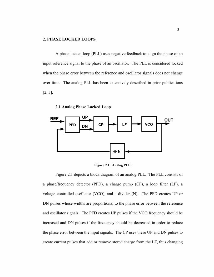
3 2. PHASE LOCKED LOOPS
A phase locked loop (PLL) uses negative feedback to align the phase of an
input reference signal to the phase of an oscillator. The PLL is considered locked
when the phase error between the reference and oscillator signals does not change
over time. The analog PLL has been extensively described in prior publications
[2, 3].
2.1 Analog Phase Locked Loop
UP REF OUT VCO LFCPPFD DN
N
Figure 2.1. Analog PLL.
Figure 2.1 depicts a block diagram of an analog PLL. The PLL consists of
a phase/frequency detector (PFD), a charge pump (CP), a loop filter (LF), a
voltage controlled oscillator (VCO), and a divider (N). The PFD creates UP or
DN pulses whose widths are proportional to the phase error between the reference
and oscillator signals. The PFD creates UP pulses if the VCO frequency should be
increased and DN pulses if the frequency should be decreased in order to reduce
the phase error between the input signals. The CP uses these UP and DN pulses to
create current pulses that add or remove stored charge from the LF, thus changing
4 the VCO control voltage. The polarity of these current pulses is dependent on
whether the VCO frequency should be increased or decreased. The output of the
LF is a regulated control voltage that is used to set the VCO frequency. The
VCO’s output is fed back to the PFD through the divider, thus closing the system
loop.
The frequency divider (N) is an optional component in the PLL. The
VCO output can be divided by a factor of N before it is fed back to the PFD. The
divider allows for frequency multiplication since the oscillator frequency will be N
times higher than the reference frequency when the PLL is locked. For increased
functionality, the division factor N could be an integer or a fractional user-
programmable number depending on the design of the divider [4].
2.2 Digital Phase Locked Loops
A digital PLL’s components, shown in Fig. 2.2, are very similar to those of
the analog PLL discussed above. The digital PLL uses a time-to-digital converter
(TDC) along with a PFD to determine the phase error sign and magnitude. The
digital loop filter (DLF) integrates the phase error information (PE) to create a
frequency error signal. The frequency and phase error signals are gain scaled and
then summed to create the DLF’s output signal. This output is used to set the
frequency of the digitally controlled analog oscillator (DCAO). The DLF replaces
the CP and LF components in the analog PLL. As in the analog PLL, a frequency
divider connected to the DCAO output may be used in the feedback path.

5
The DPLL is becoming increasingly more desirable than analog PLLs for
the following reasons. As deep submicron processes become available, a DPLL
design can be easily scaled into the new process. The DPLL is also easier to test
because the digital error signals can be accurately monitored. The digital control
word in a DLF is less susceptible to noise than the analog voltage present in the
LF. Finally, digital circuits are also less susceptible to noise.
REF OUT PEPFD & DCO DLF TDC
N
Figure 2.2. Digital PLL.
6
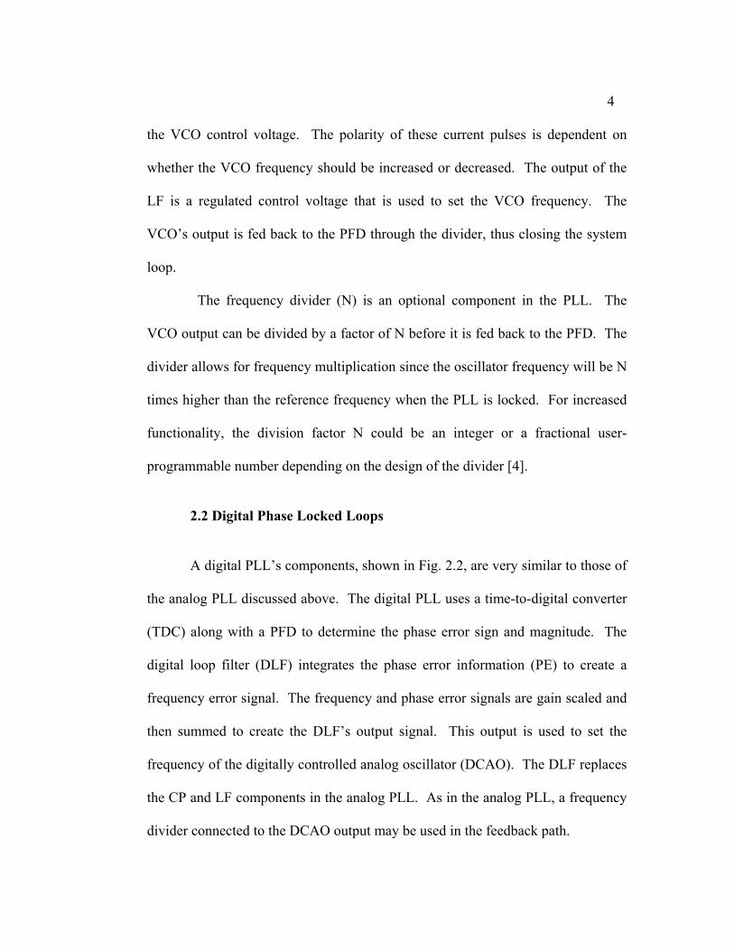
3. CHARACTERIZATION OF A DPLL
A digital PLL with the components described above was designed and
fabricated in a 0.35µm technology SOI process [5]. This DPLL uses a digitally
controlled analog oscillator (DCAO) that converts the digital controlling word into
two analog signals with two 6 bit digital to analog converters (DACs) [6]. These
two signals create fine and coarse tuning controls for the oscillator (Fig. 3.1). The
motivation for doing this is that a 12 bit DAC with a single tuning control is much
harder to design than two 6 bit DACs with two tuning controls.
DAC VCO
CTRL<12:7>
DAC
CTRL<6:1>
Ifine
Icoarse
Coarse
Fine
Out
In<6:1>
Bias
Bias
Out
Out
In<6:1>
CTRL<12:1>
DAC VCO
CTRL<12:7>
DAC
CTRL<6:1>
Ifine
Icoarse
Coarse
Fine
Out
In<6:1>
Bias
Bias
Out
Out
In<6:1>
CTRL<12:1>
Figure 3.1. Digitally controlled analog oscillator block diagram.
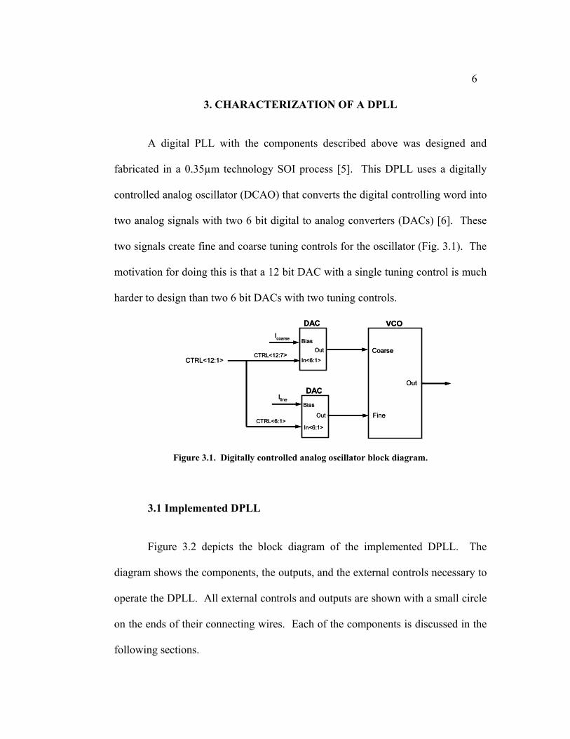
3.1 Implemented DPLL Figure 3.2 depicts the block diagram of the implemented DPLL. The
diagram shows the components, the outputs, and the external controls necessary to
operate the DPLL. All external controls and outputs are shown with a small circle
on the ends of their connecting wires. Each of the components is discussed in the
following sections.
7
Buffers
Ref_In PFD & TDC
Ref_Out DLFRef
Div_Out T<10:1> PE<10:1>Div
CTRL<10:1>Clk Clk
VG1
DCAOVG2
I_fine I_coarse
CTRL<10:1>
Divider
CTRL<12>Out InCTRL<11>
div1div0
VCO_out
Figure 3.2. Implemented DPLL block diagram.
3.2 PFD and TDC
The PFD used in the DPLL is no different from that of an analog PLL. The
PFD’s pulse widths are analog signals that represent the phase error between the
input signals. A TDC is used to create a binary word that represents these pulse
widths. The TDC’s output only defines the magnitude of the phase error and an
additional logic circuit is required to determine the sign of the phase error. The
sign of the phase error arises from which input clock signal arrives first.
Assuming the two input clock signals have the same frequency, the time difference
that is represented is proportional to the phase difference between these clocks.
8
A phase detector alone is not sufficient for use in a PLL design. The use of
a phase/frequency detector is necessary in order to avoid false frequency locking
[2]. A PLL using only a phase detector would allow false frequency locking since
there are usually both phase and frequency errors present between the reference
and oscillator signals.
The most common TDC uses a chain of non-inverting delay cells to
measure the phase difference of the rising edge transitions of the input clocks. The
delay chain propagates a signal starting when either input clock’s rising edge
transition occurs. The delay chain is sampled by flip flops when the second clock
input has its rising edge transition. The flip flops generate a digital word depicting
how many delay cells propagated the signal between the rising edges of the two
input clocks. The digital word created is thermometer coded and is often
converted into binary to simplify hardware used in the controller block.
There are two common ways that the delay elements of a TDC are sized.
All of the elements in the delay chain can have equal sizing [7] or they can have
exponential sizing [8]. If the delay chain contains equally sized elements, the
quantization error of each element remains small. The exponential delay chain, on
the other hand, has increasing quantization error across the elements but it can
measure a larger time range using the same number of elements as an equally sized
delay chain.
9
R U
V D
PFD
∆T ∆T ∆T 4∆T 8∆T 16∆T 32∆T 64∆T 128∆T
D QSign
D1 D2 D3 D4 D5 D6 D7 D8 D9
Pseudo-Thermometer Encoder
Q<9:1>
PE<10:1>
Flip Flops
Variable Delays
R U
V D
PFD
∆T ∆T ∆T 4∆T 8∆T 16∆T 32∆T 64∆T 128∆T
D QSign
D1 D2 D3 D4 D5 D6 D7 D8 D9
Pseudo-Thermometer Encoder
Q<9:1>
PE<10:1>
Flip Flops
Variable Delays
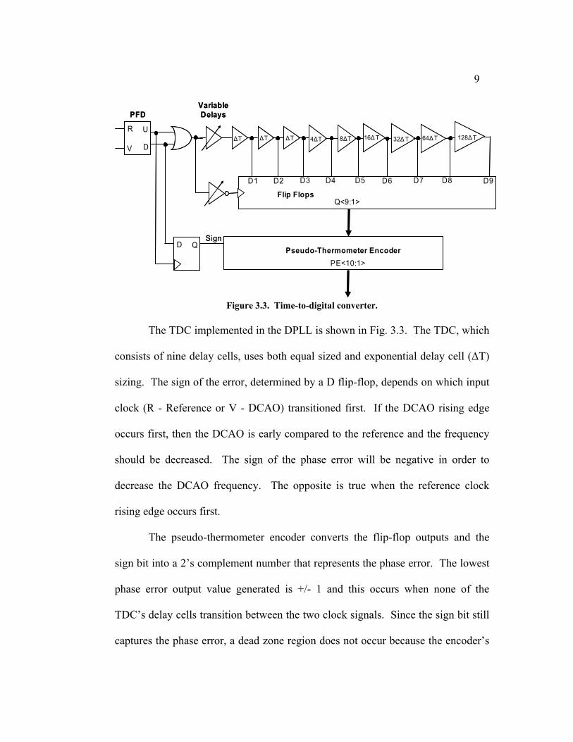
Figure 3.3. Time-to-digital converter.
The TDC implemented in the DPLL is shown in Fig. 3.3. The TDC, which
consists of nine delay cells, uses both equal sized and exponential delay cell (∆T)
sizing. The sign of the error, determined by a D flip-flop, depends on which input
clock (R - Reference or V - DCAO) transitioned first. If the DCAO rising edge
occurs first, then the DCAO is early compared to the reference and the frequency
should be decreased. The sign of the phase error will be negative in order to
decrease the DCAO frequency. The opposite is true when the reference clock
rising edge occurs first.
The pseudo-thermometer encoder converts the flip-flop outputs and the
sign bit into a 2’s complement number that represents the phase error. The lowest
phase error output value generated is +/- 1 and this occurs when none of the
TDC’s delay cells transition between the two clock signals. Since the sign bit still
captures the phase error, a dead zone region does not occur because the encoder’s
10 output is always nonzero. Thus, the highest phase error output from the encoder is
+/- 256 and this occurs when all of the delay cells have transitioned.
The variable delays in the TDC are controlled by VG1 and VG2 from Fig.
3.2. These controls are present to balance the time delays of the two paths
branching out from the OR gate. Mainly, the delay adjustment compensates for
the constant phase error introduced by the PFD’s reset pulse.
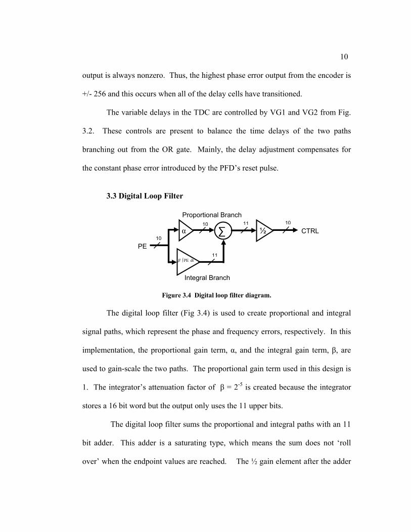
3.3 Digital Loop Filter
dt PE∫β
Proportional Branch101110
CTRL ∑α ½10
PE 11
Integral Branch
Figure 3.4 Digital loop filter diagram. The digital loop filter (Fig 3.4) is used to create proportional and integral
signal paths, which represent the phase and frequency errors, respectively. In this
implementation, the proportional gain term, α, and the integral gain term, β, are
used to gain-scale the two paths. The proportional gain term used in this design is
1. The integrator’s attenuation factor of β = 2-5 is created because the integrator
stores a 16 bit word but the output only uses the 11 upper bits.
The digital loop filter sums the proportional and integral paths with an 11
bit adder. This adder is a saturating type, which means the sum does not ‘roll
over’ when the endpoint values are reached. The ½ gain element after the adder
11 is realized by using only the 10 upper bits of the adder. These remaining 10 bits
are converted from two’s complement into offset binary notation which becomes
the control word for the DCAO.
In [9], it was concluded that the smallest phase change of the proportional
branch should be much larger than the smallest phase change of the integral
branch. This ratio is referred to as the stability factor which is shown below.
3221
integral alproportionFactorStability 5 === −∆θ
∆θ (3.1)
This is a low stability factor value, which results in an under-damped
response of the PLL due to a frequency step.
3.4 Digitally Controlled Analog Oscillator
The DCAO is a three stage delay cell with the Lee/Kim [10] structure. The
DCAO output is rail to rail which is beneficial because this minimizes the effect
that noise has on the output. Each of the delay cell stages has a differential output
in order to increase the power supply rejection ratio. A single ended output from
the delay cell’s differential output is connected to the programmable divider for
use in the feedback loop.
The implemented DCAO differs slightly from the Lee/Kim structure, in
that an additional pair of auxiliary transistors was added to create both fine and
coarse tuning. The fine and coarse tuning DACs create analog voltages that are
used to drive the tuning transistors of the DCAO, which controls the oscillation
frequency. The oscillation frequency is controlled by a 12 bit word where the
12 controller supplies the lower 10 bits, and the most significant two bits are
externally controlled as shown in Fig. 3.2. Both of the DACs are six bit, where the
lower 6 bits use the fine DAC and the upper 6 bits use the coarse DAC. The fine
and coarse DAC gains are controlled by the external bias currents Ifine and Icoarse,
respectively.
Although not shown in the block diagram of Fig. 3.2, a multiplexer exists
between the DLF’s output and the DCAO’s control word input. The multiplexer
allows the DCAO’s input control word to be externally created (open loop) or
determined by the DLF (closed loop). This multiplexer allows the DCAO to be
characterized out of the loop, which is beneficial for understanding the DPLL
operation.
3.5 Divider Circuit
The PLL loop contains an externally programmable DCAO divider. The
divider can be set to produce the following divisions of the DCAO signal: (64, 32,
16, and 8). Two digital input signals (div0 and div1) control the divider ratio by
simply switching D flip-flop divide-by-two stages into or out of the signal path as
necessary.
3.6 DPLL Analysis
The frequency steps of the DCAO are produced by the proportional and
integral paths. The step size depends on the following parameters: proportional
13 path gain, integral path gain, DCAO gain from the fine DAC, DCAO gain from the
coarse DAC, the current phase error, and the current integrator value. The value of
the resulting control word determines what portions of the fine and coarse DACs
are to be utilized. The upper 6 bits of CTRL use the coarse DAC and the lower 6
bits use the fine DAC.
In [5], the equations governing the DPLL are derived from a continuous
time analog PLL. These equations can be used if the loop bandwidth is less than
1/10th of the PFD’s update frequency. From these equations, the unity gain
bandwidth and phase margin can be estimated for the operating conditions used in
the measurements. The values for this DPLL will be discussed in Section 3.9.
)(φtan1N
FKω M
2RdigUGB +
= (3.2)
= −
Z
UGB1M ω
ωtanφ (3.3)
RLSBR
ndig TfT
TGK
∆
= (3.4)
where, FR is the reference frequency, TR = 1/ FR, flsb is the smallest DCAO
frequency step size, and Gn = 0.5.
The selection of the PLL’s loop bandwidth is critical to the overall system
performance. A low bandwidth PLL has the best ability to filter input jitter and
also a high bandwidth PLL is necessary to reduce jitter from the VCO [11]. This
obviously leads to a trade off because both criteria cannot be met. The designer
must select a loop bandwidth to best fit the desired specifications.
14
3.7 Simulations
Each block of the DPLL was individually simulated with Spectre to verify
proper operation and expectations. The simulation results were also used to
determine the approximate current and voltage bias conditions that would be used
when measuring the fabricated test chips. From this information, biasing resistor
sizes, or their range, could be determined so properly sized trimpots and resistors
could be populated on the PCB. A DCAO tuning curve and an oscillator phase
noise plot were also generated for comparison with the measured values.
3.8 Initial IC Testing and Findings
It was found that the DPLL was able to lock to the reference signal but
only if the reference was a sine wave with a small amplitude centered at Vdd/2.
The use of a sine wave reference was not obvious since a square wave reference
signal indicated no problems in simulation. Also, the necessary reference
amplitude of ~500mV pk-pk was unexpected.
These special conditions, necessary to make the DPLL lock, seem to
suggest that the input signals are coupling into other parts of the circuit. The
source of the coupling is most likely the input/output buffers shown in Fig. 3.2.
Since a sine wave has a more gradual rise and fall time than a square wave of the
same frequency, a sine wave reference would, therefore, allow the input buffer to
switch states slowly. When the buffer switches states slower, it consumes less
15 current. It is assumed that the fast transition of a reference square wave is causing
the buffer to have a higher switching current. These current spikes are likely
creating noise and glitches that affect other circuits which cause the DPLL to not
reach a locked state.
Also, it was found that 50Ω termination was required for all three of the
input/output buffers. If one of these signals was not buffered, the circuit could not
reach a locked state. This seems to indicate that signal coupling from the buffer
signals was occurring.
The divide-by-N circuit was found to produce proper division rates of the
DCAO output for the divide by 64, 32, and16 settings. The divide by 8 did not
properly divide the DCAO’s output. The high switching speed and buffer issue
described above may account for the problems with this divider setting.
3.9 Comparison of Measured and Simulated Results
In Fig. 3.5, the results of a phase noise measurement and simulation
performed for a divided DCAO (N=32) free-running frequency of 29.28 MHz are
shown. As the figure indicates, the offset frequency where the phase noise roll-off
changes from -30dBc/decade to -20dBc/decade is the same in both measurement
and simulation. The slope change occurs approximately at a 10 kHz offset
frequency where flicker noise (1/f ) is no longer the dominant noise source. The
phase noise is due to white noise for frequency offsets greater than 10 kHz. The
phase noise at 10 kHz was simulated to be -71.76 dBc/Hz but was measured to be
16 -66.53 dBc/Hz. At 100 kHz, the phase noise was simulated to be -96.16 dBc/Hz
but was measured to be -95.81 dBc/Hz. The measured values are slightly worse
than what was simulated. The phase noise simulation was performed with
noiseless power supplies, control signals, and bias currents along with matched
transistor devices. The differences between the measured and simulated values are
likely attributed to these idealities used in the simulations.

17
(a)
102
103
104
105
106
-120
-100
-80
-60
-40
-20
0
Frequency Offset (Hz)
dBc/
Hz
(b)
Figure 3.5 Phase noise measurement and simulation.
(a) Measurement, and (b) simulation for a divided DCAO frequency of 29.28 MHz.
18
0 100 200 300 400 500 600 700 800 900 1000650
700
750
800
850
900
950
1000
Decimal Codes
Freq
uenc
y (M
Hz)
MeasuredSimulated
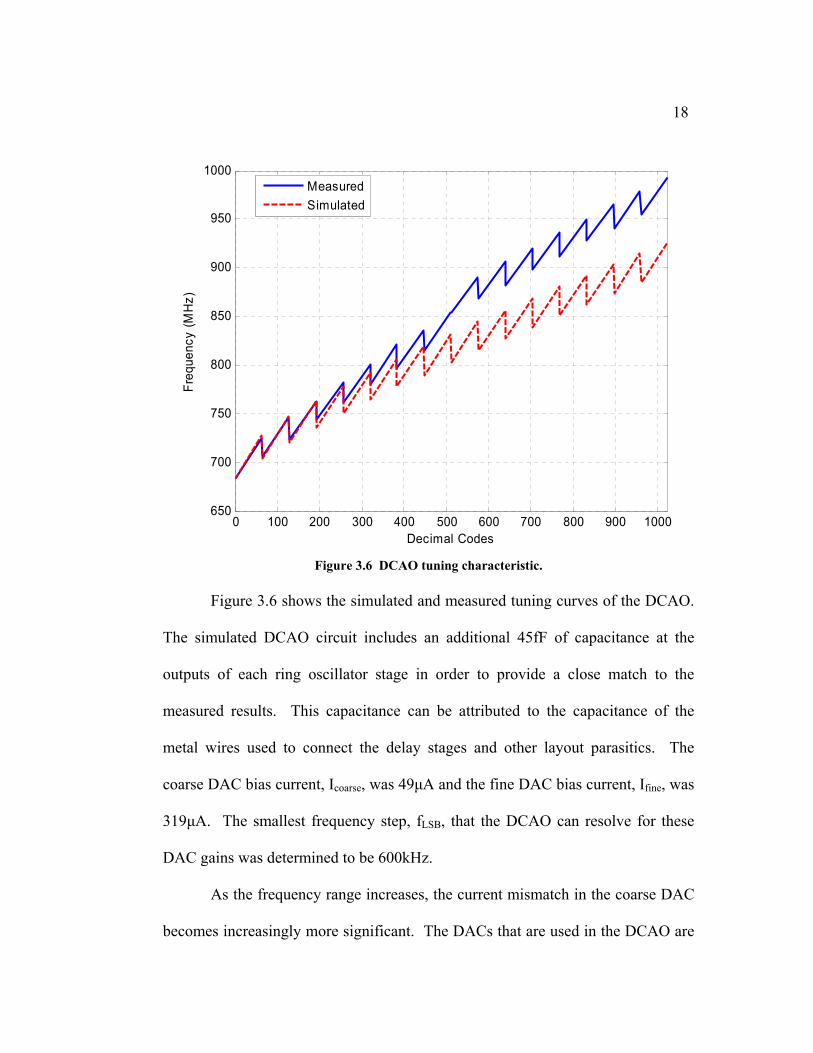
Figure 3.6 DCAO tuning characteristic.
Figure 3.6 shows the simulated and measured tuning curves of the DCAO.
The simulated DCAO circuit includes an additional 45fF of capacitance at the
outputs of each ring oscillator stage in order to provide a close match to the
measured results. This capacitance can be attributed to the capacitance of the
metal wires used to connect the delay stages and other layout parasitics. The
coarse DAC bias current, Icoarse, was 49µA and the fine DAC bias current, Ifine, was
319µA. The smallest frequency step, fLSB, that the DCAO can resolve for these
DAC gains was determined to be 600kHz.
As the frequency range increases, the current mismatch in the coarse DAC
becomes increasingly more significant. The DACs that are used in the DCAO are
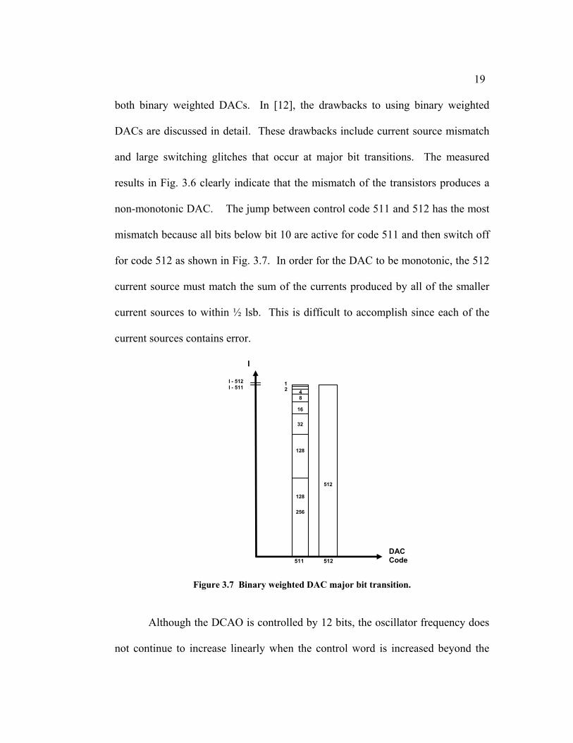
19 both binary weighted DACs. In [12], the drawbacks to using binary weighted
DACs are discussed in detail. These drawbacks include current source mismatch
and large switching glitches that occur at major bit transitions. The measured
results in Fig. 3.6 clearly indicate that the mismatch of the transistors produces a
non-monotonic DAC. The jump between control code 511 and 512 has the most
mismatch because all bits below bit 10 are active for code 511 and then switch off
for code 512 as shown in Fig. 3.7. In order for the DAC to be monotonic, the 512
current source must match the sum of the currents produced by all of the smaller
current sources to within ½ lsb. This is difficult to accomplish since each of the
current sources contains error.
I
I - 512 1I - 511 2
Figure 3.7 Binary weighted DAC major bit transition.
Although the DCAO is controlled by 12 bits, the oscillator frequency does
not continue to increase linearly when the control word is increased beyond the
16
DAC Code
128
256
84
32 128
512
511 512
20 shown 10 bit range. Since the upper two bits are externally controlled, the
nonlinear region can be avoided. The biasing currents for the fine and coarse
DACs could be adjusted to produce a large set of turning curves. However, all of
these curves still contain the mismatch issue described above.
0 0.02 0.04 0.06 0.08 0.1 0.12 0.14 0.16 0.18 0.2-0.05
0
0.05
0.1
0.15
Vol
ts
Time (microseconds)
0 0.02 0.04 0.06 0.08 0.1 0.12 0.14 0.16 0.18 0.2-0.05
0
0.05
0.1
0.15
Vol
ts
Time (microseconds)
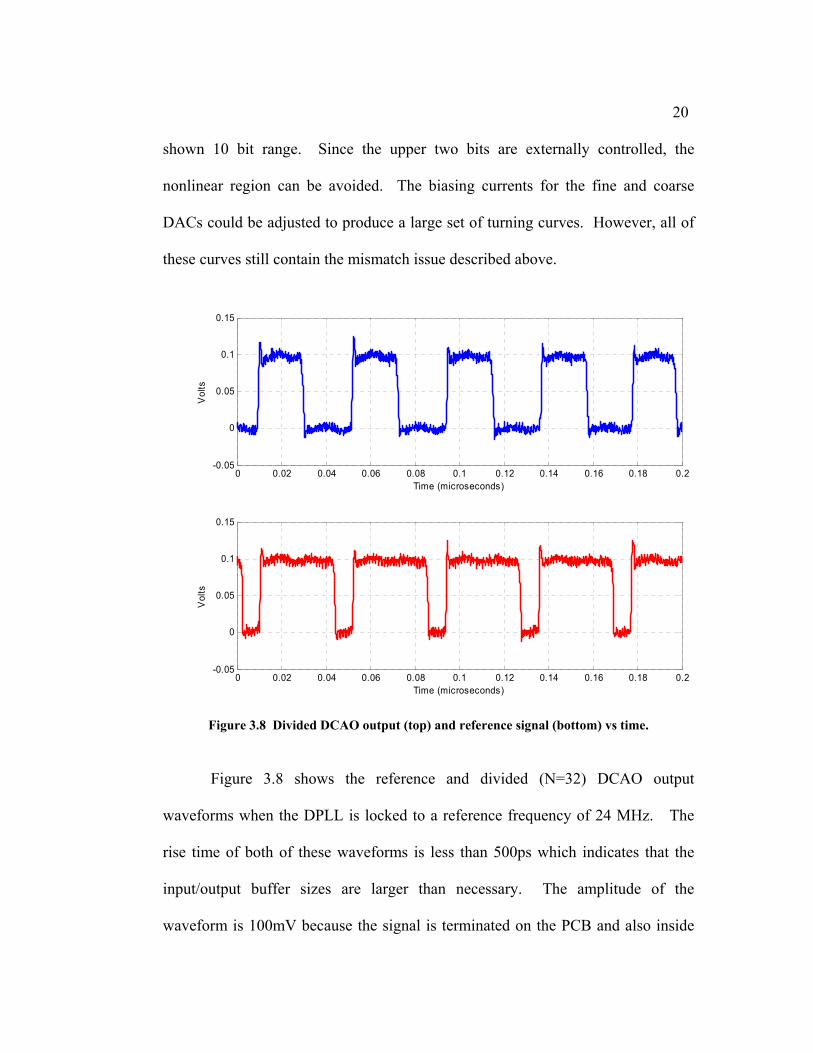
Figure 3.8 Divided DCAO output (top) and reference signal (bottom) vs time.
Figure 3.8 shows the reference and divided (N=32) DCAO output
waveforms when the DPLL is locked to a reference frequency of 24 MHz. The
rise time of both of these waveforms is less than 500ps which indicates that the
input/output buffer sizes are larger than necessary. The amplitude of the
waveform is 100mV because the signal is terminated on the PCB and also inside
21 the oscilloscope. The ringing present on the rising edges of the waveforms could
be due to the oversized buffers or possibly cable reflections. Additionally, the
duty cycle of the reference signal has been altered by the inverter stages in the
DPLL’s reference buffers. This is because the input amplitude of the reference
signal is very small which increases the duty cycle’s dependence on the inverter
trip point. From simulation, the duty cycle shown in this figure could result from a
Vt mismatch of approximately 85mV in the initial inverter stage.
0 0.5 1 1.5 2 2.5 3 3.5 4 4.5 5-4
-2
0
2
4
Pha
se W
ord
Time (microseconds)
0 0.5 1 1.5 2 2.5 3 3.5 4 4.5 5273
274
275
276
277
278
279
Time (microseconds)
CTR
L W
ord
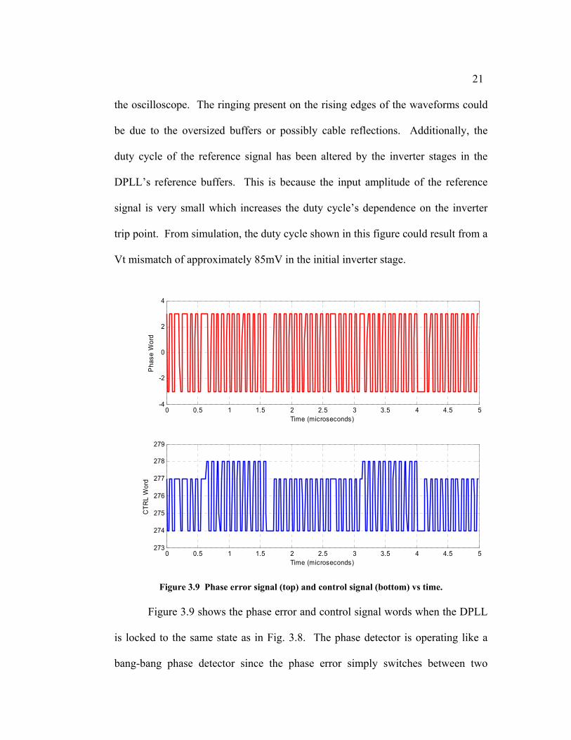
Figure 3.9 Phase error signal (top) and control signal (bottom) vs time.
Figure 3.9 shows the phase error and control signal words when the DPLL
is locked to the same state as in Fig. 3.8. The phase detector is operating like a
bang-bang phase detector since the phase error simply switches between two
22 values. The step between control word values of 277 and 278 is caused by the
integrator. Since the integrator stores 16 bits but only outputs the upper 11 bits,
the frequency error accumulating in the lower 5 bits does not affect the DPLL loop
until it becomes large enough to change the higher bits. At this point, the
frequency error value of the loop is updated. This creates the switching pattern
between the control word values of 277 and 278. Since the integrator is switching
between two values, it means that both positive and negative frequency errors are
being captured, as would be expected when the DPLL is locked.
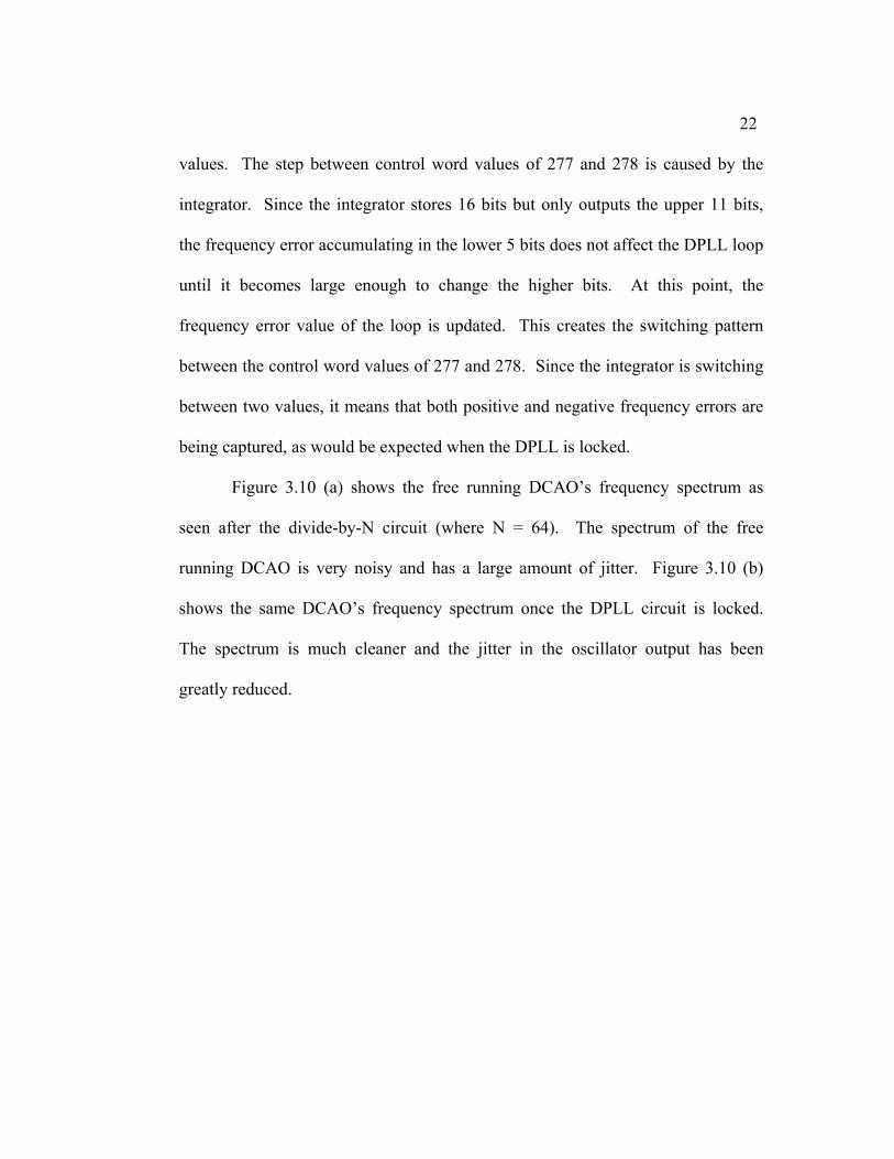
Figure 3.10 (a) shows the free running DCAO’s frequency spectrum as
seen after the divide-by-N circuit (where N = 64). The spectrum of the free
running DCAO is very noisy and has a large amount of jitter. Figure 3.10 (b)
shows the same DCAO’s frequency spectrum once the DPLL circuit is locked.
The spectrum is much cleaner and the jitter in the oscillator output has been
greatly reduced.
23
11.9 11.95 12 12.05 12.1-100
-90
-80
-70
-60
-50
-40
-30
-20
-10
0
dB
Frequency (MHz)
(a)
11.9 11.95 12 12.05 12.1-100
-90
-80
-70
-60
-50
-40
-30
-20
-10
0
dB
Frequency (MHz)
(b)
Figure 3.10 Frequency spectrum of the DCAO output – divide by 64. (a) Free running DCAO. (b) DCAO in DPLL.
24
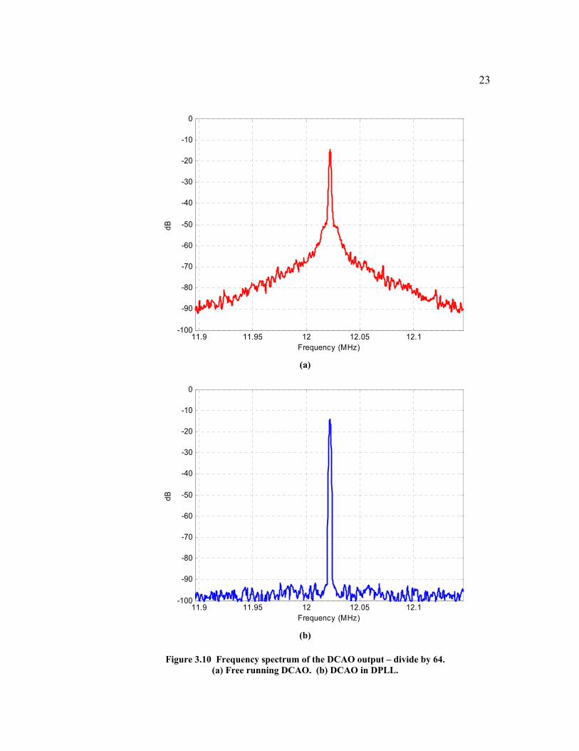
Figure 3.11 Jitter Histogram of DPLL
The obtained jitter distribution shown in Fig. 3.11 was measured when the
DPLL was locked to a 24MHz reference with a divider setting of N=32. This was
the best case jitter obtained for any of the divider settings. When looking at the
measured sigma distribution percentages, we can see they are close to the true
Gaussian percentages.
Using the measured data, the DPLL’s loop bandwidth can be approximated
from the equations in Section 3.6 along with FR = 24 MHz, N = 32, and fLSB =
600kHz. The calculated loop bandwidth was found to be 400 kHz and the phase
margin was 73º. Since the bandwidth is much less than 1/10th of the PFD’s update
25 frequency, the continuous time PLL equations are valid for approximating the
DPLL’s behavior which confirms that the DPLL loop is stable.
26
4. STOCHASTIC TIME TO DIGITAL CONVERTER
In order to reduce noise in a DPLL, it is desirable to have a small
quantization error of the PFD’s pulse width. The smallest time step that a TDC,
like the one described previously, can measure is dependent on the speed of the
delay cells which are constructed with inverters. The stochastic time-to-digital
converter (STDC) was designed to measure time differences that are smaller than
the delay time of an inverter [14]. The addition of an STDC in a DPLL should
improve the jitter performance.
4.1 Quantization of Phase Error
The fastest delay cell that can be constructed is an inverter, thus the
inverter’s propagation time is the smallest measurable time step in a traditional
TDC. In the 0.35µm process, this propagation time is at least 80ps. Fig. 4.1
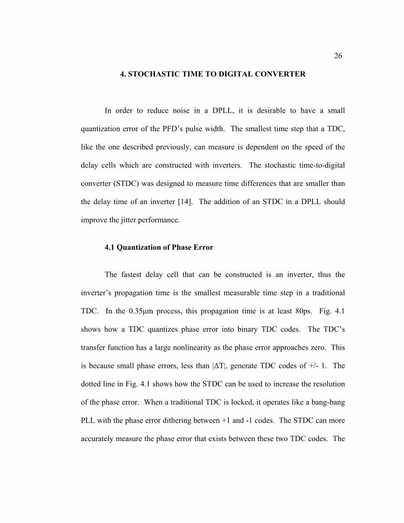
shows how a TDC quantizes phase error into binary TDC codes. The TDC’s
transfer function has a large nonlinearity as the phase error approaches zero. This
is because small phase errors, less than |∆T|, generate TDC codes of +/- 1. The
dotted line in Fig. 4.1 shows how the STDC can be used to increase the resolution
of the phase error. When a traditional TDC is locked, it operates like a bang-bang
PLL with the phase error dithering between +1 and -1 codes. The STDC can more
accurately measure the phase error that exists between these two TDC codes. The
27 STDC is designed to supplement a DPLL by creating a fine control loop that
would be used for higher accuracy when the loop is locked to the reference signal.
+1
+2
-1
-2
∆T 2∆T∆θe
-∆T-2∆T
TDC Code
TDC
Statistical TDC
+1
+2
-1
-2
∆T 2∆T∆θe
-∆T-2∆T
TDC Code
TDC
Statistical TDC
Figure 4.1 Quantization of phase error for TDCs.
Although a TDC can be designed with inverting delay cells, many
designers create TDCs with non-inverting delay cells because of differences in the
inverter rise and fall time characteristics. These differences create inaccuracies
when resolving the phase error. By using non-inverting delay cells, the smallest
time step of the TDC is even larger than the propagation time of an inverter.
Recently, [7] proposed a pseudo-differential TDC that uses inverting delay cells
and avoids the described mismatch between even and odd delay stages.
4.2 Theory of Operation of the STDC
The STDC relies on mismatches of arbiters to help measure small time
steps of the phase error. An arbiter can be used to determine which of two clock
signals had its rising edge first. Transistor mismatch in this arbiter circuit creates
28 an offset voltage between the arbiter’s inputs which introduces a small error.
When determining which rising edge occurred first, the offset voltage is
effectively equivalent to time delaying one of the input signals by a finite amount.
The original concept of this system was described in [13], where an array of
arbiters calibrated a flash TDC. The STDC design, on the other hand, uses the
sum of a group of arbiter outputs to determine the time difference between the
signals in the DPLL [14].
The STDC design contains 84 independent arbiters, each connected to the
two clock signals for which the time difference has to be measured. The output
states of the arbiters are either high or low, depending on which clock signal had
its rising edge first. The arbiter’s output is reset every time both of the clock
signals become grounded. In a DPLL, the arbiter determines if the VCO clock
signal is ‘early’ or ‘late’ when compared to the reference clock signal.
Each of these 84 arbiters has an input offset voltage due to the IC
fabrication process. The offset voltage is assumed to have a statistical distribution.
When the phase error between the input signals is small, the offset voltage will
affect which output state is reached. By summing together the arbiter outputs, the
number of output states that are in the majority can be used to create a fine time
estimation of the phase error.
29
4.3 Design Limitations
Some of the factors that can limit the STDC’s performance include the size
of the standard deviation of offset voltage, the input signal rise time, the number of
arbiters used, and the speed of the hardware used to sum the arbiter outputs.
The size of the standard deviation helps to determine the time range over
which the STDC can provide relevant information. If the time difference falls
outside of this range, all of the arbiters will produce exactly the same output and
the circuit will behave much like a bang-bang phase detector. For a fixed number
of arbiters, an increase in the standard deviation of the offset voltage will result in
a larger measurable time range. The downside to this is that the resolution of the
STDC will decrease as the arbiter offsets are distributed farther out in voltage
resulting in a farther spread in time.
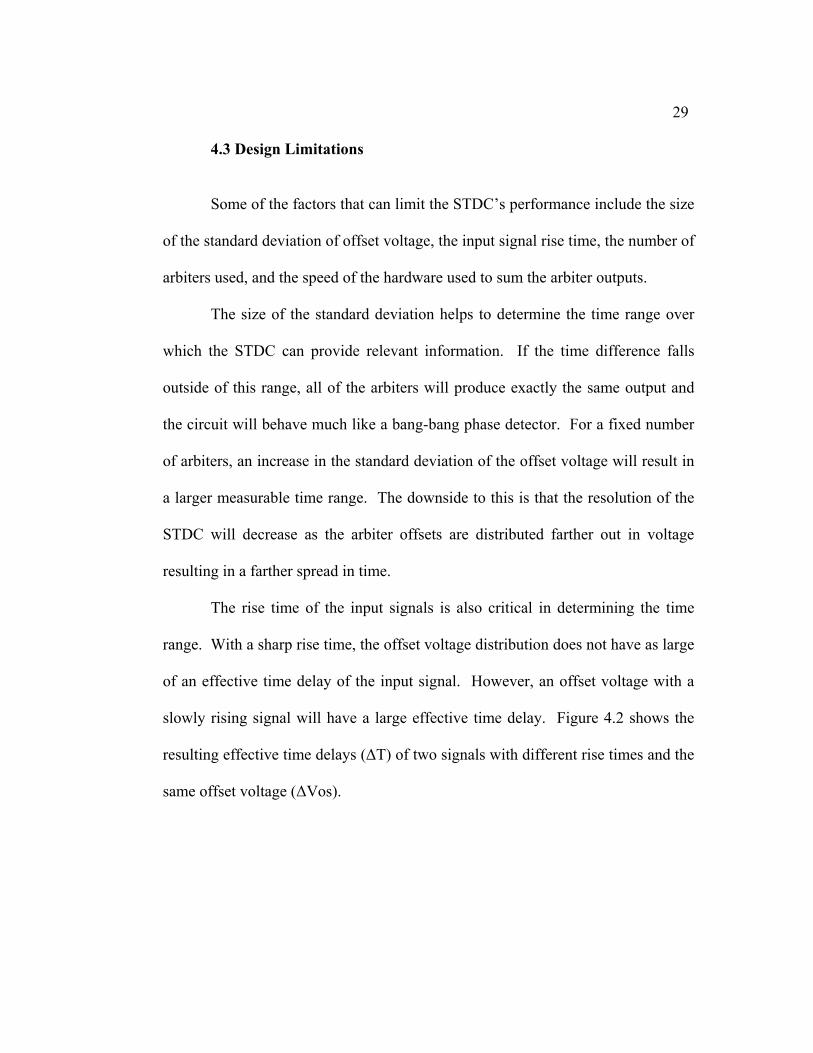
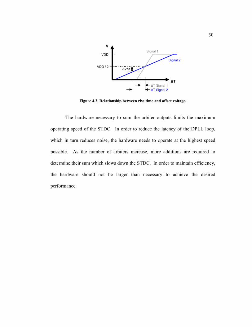
The rise time of the input signals is also critical in determining the time
range. With a sharp rise time, the offset voltage distribution does not have as large
of an effective time delay of the input signal. However, an offset voltage with a
slowly rising signal will have a large effective time delay. Figure 4.2 shows the
resulting effective time delays (∆T) of two signals with different rise times and the
same offset voltage (∆Vos).
30
V Signal 1
VDD
Signal 2
VDD / 2∆Vos
∆T ∆T Signal 1
∆T Signal 2
Figure 4.2 Relationship between rise time and offset voltage.
The hardware necessary to sum the arbiter outputs limits the maximum
operating speed of the STDC. In order to reduce the latency of the DPLL loop,
which in turn reduces noise, the hardware needs to operate at the highest speed
possible. As the number of arbiters increase, more additions are required to
determine their sum which slows down the STDC. In order to maintain efficiency,
the hardware should not be larger than necessary to achieve the desired
performance.
31
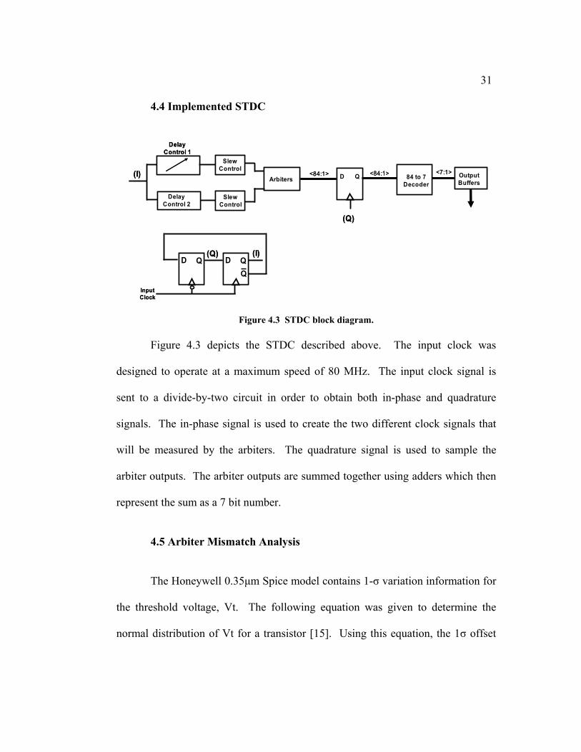
4.4 Implemented STDC
Delay Control 1
SlewControl
Arbiters D Q<84:1> <84:1> 84 to 7Decoder
OutputBuffers
D Q D Q
<7:1>
InputClock
Q
(I)(Q)
SlewControl
Delay Control 2
(I)
(Q)
Delay Control 1
SlewControl
Arbiters D Q<84:1> <84:1> 84 to 7Decoder
OutputBuffers
D Q D Q
<7:1>
InputClock
Q
(I)(Q)
SlewControl
Delay Control 2
(I)
(Q)
Figure 4.3 STDC block diagram. Figure 4.3 depicts the STDC described above. The input clock was
designed to operate at a maximum speed of 80 MHz. The input clock signal is
sent to a divide-by-two circuit in order to obtain both in-phase and quadrature
signals. The in-phase signal is used to create the two different clock signals that
will be measured by the arbiters. The quadrature signal is used to sample the
arbiter outputs. The arbiter outputs are summed together using adders which then
represent the sum as a 7 bit number.
4.5 Arbiter Mismatch Analysis
The Honeywell 0.35µm Spice model contains 1-σ variation information for
the threshold voltage, Vt. The following equation was given to determine the
normal distribution of Vt for a transistor [15]. Using this equation, the 1σ offset
32 voltage distribution was calculated to be less than 20mV for the input transistor
used in the arbiter circuit.
3108.0
L*W46.3mV)(in 1σ
⋅
+= - W and L are in microns (4.1)
In [16], the author claims that Vt mismatch doesn’t follow Area1 when
transistor geometries are wide/short and narrow/long and a more accurate model is
proposed. The parameters required to use this more accurate model were not
available and not necessary for proving the STDC concept.
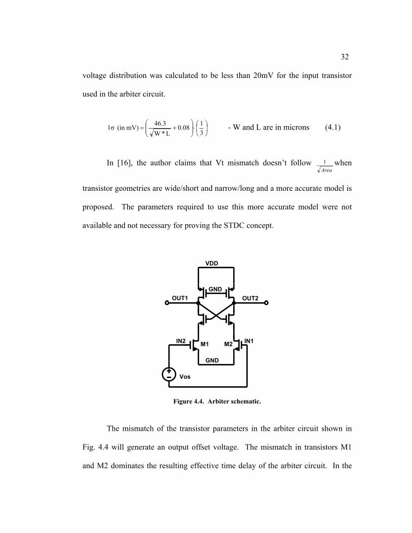
VDD
GNDOUT1 OUT2
IN2 IN1 M1 M2
GND
Vos
Figure 4.4. Arbiter schematic.
The mismatch of the transistor parameters in the arbiter circuit shown in
Fig. 4.4 will generate an output offset voltage. The mismatch in transistors M1
and M2 dominates the resulting effective time delay of the arbiter circuit. In the
33 schematic, the voltage source Vos is applied to the circuit input in order to cancel
the output offset.
The analysis of mismatch in [17] describes the mutually independent
components related to mismatch and also provides approximate percent variations.
This information can be used to analyze the offset voltage of the arbiter circuit.
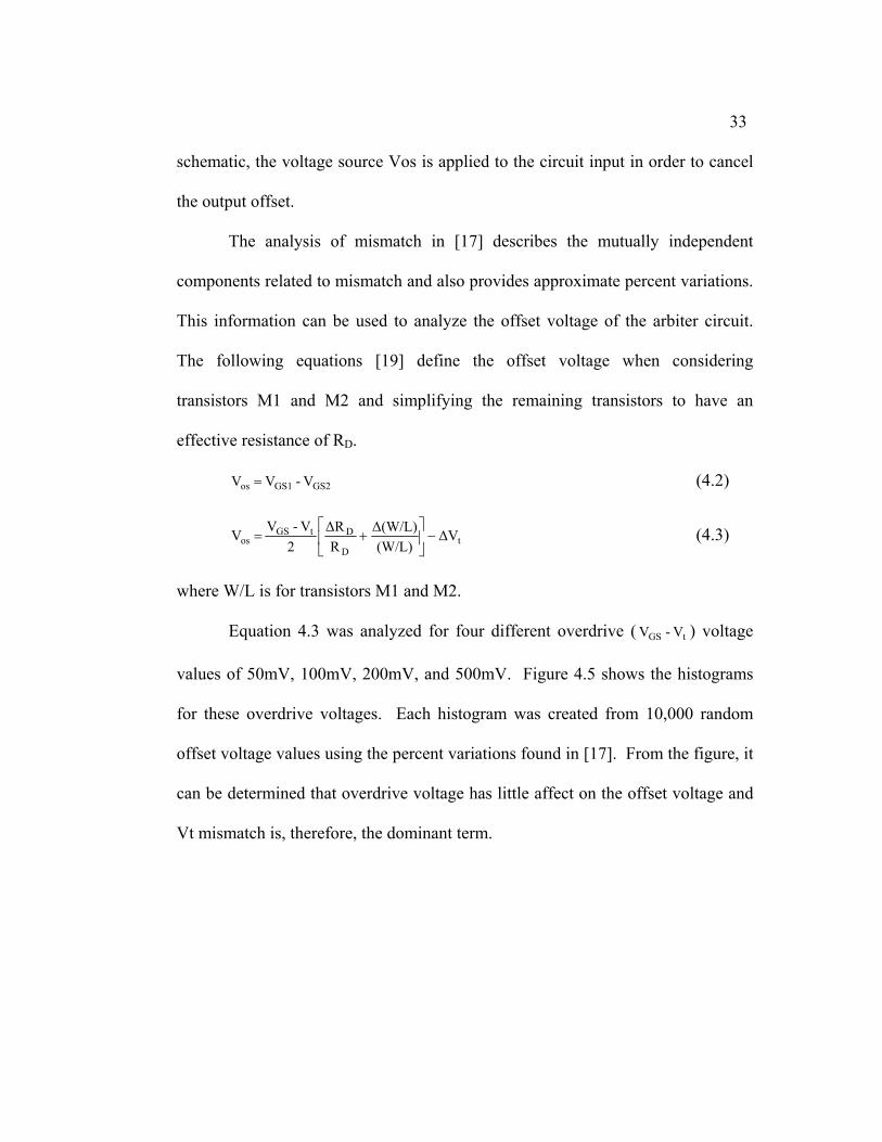
The following equations [19] define the offset voltage when considering
transistors M1 and M2 and simplifying the remaining transistors to have an
effective resistance of RD.
GS2GS1os V - V V = (4.2)
tD
DtGSos ∆V
(W/L)∆(W/L)
R∆R
2V - V V −
+= (4.3)
where W/L is for transistors M1 and M2.
Equation 4.3 was analyzed for four different overdrive ( V ) voltage
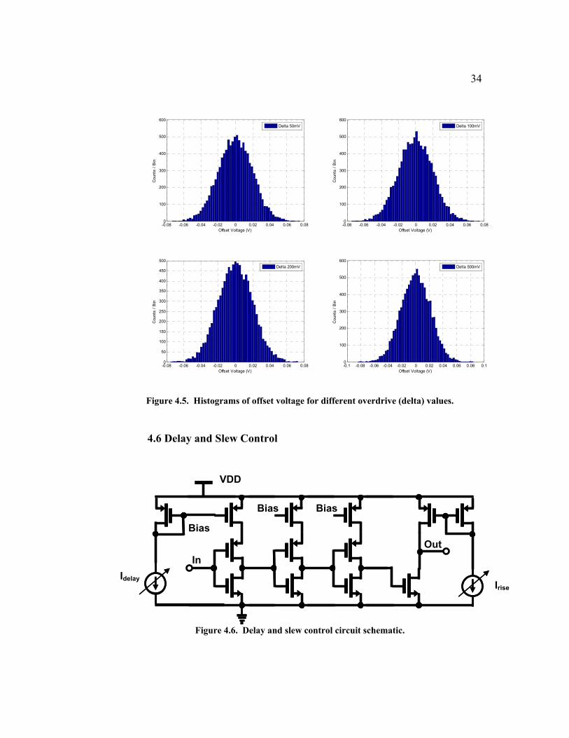
values of 50mV, 100mV, 200mV, and 500mV. Figure 4.5 shows the histograms
for these overdrive voltages. Each histogram was created from 10,000 random
offset voltage values using the percent variations found in [17]. From the figure, it
can be determined that overdrive voltage has little affect on the offset voltage and
Vt mismatch is, therefore, the dominant term.
tGS V -
34
-0.08 -0.06 -0.04 -0.02 0 0.02 0.04 0.06 0.080
100
200
300
400
500
600
Offset Voltage (V)
Cou
nts
/ Bin
Delta 50mV
-0.08 -0.06 -0.04 -0.02 0 0.02 0.04 0.06 0.080
100
200
300
400
500
600
Offset Voltage (V)
Cou
nts
/ Bin
Delta 100mV
-0.08 -0.06 -0.04 -0.02 0 0.02 0.04 0.06 0.080
50
100
150
200
250
300
350
400
450
500
Offset Voltage (V)
Cou
nts
/ Bin
Delta 200mV
-0.1 -0.08 -0.06 -0.04 -0.02 0 0.02 0.04 0.06 0.08 0.10
100
200
300
400
500
600
Offset Voltage (V)
Cou
nts
/ Bin
Delta 500mV
Figure 4.5. Histograms of offset voltage for different overdrive (delta) values.
4.6 Delay and Slew Control
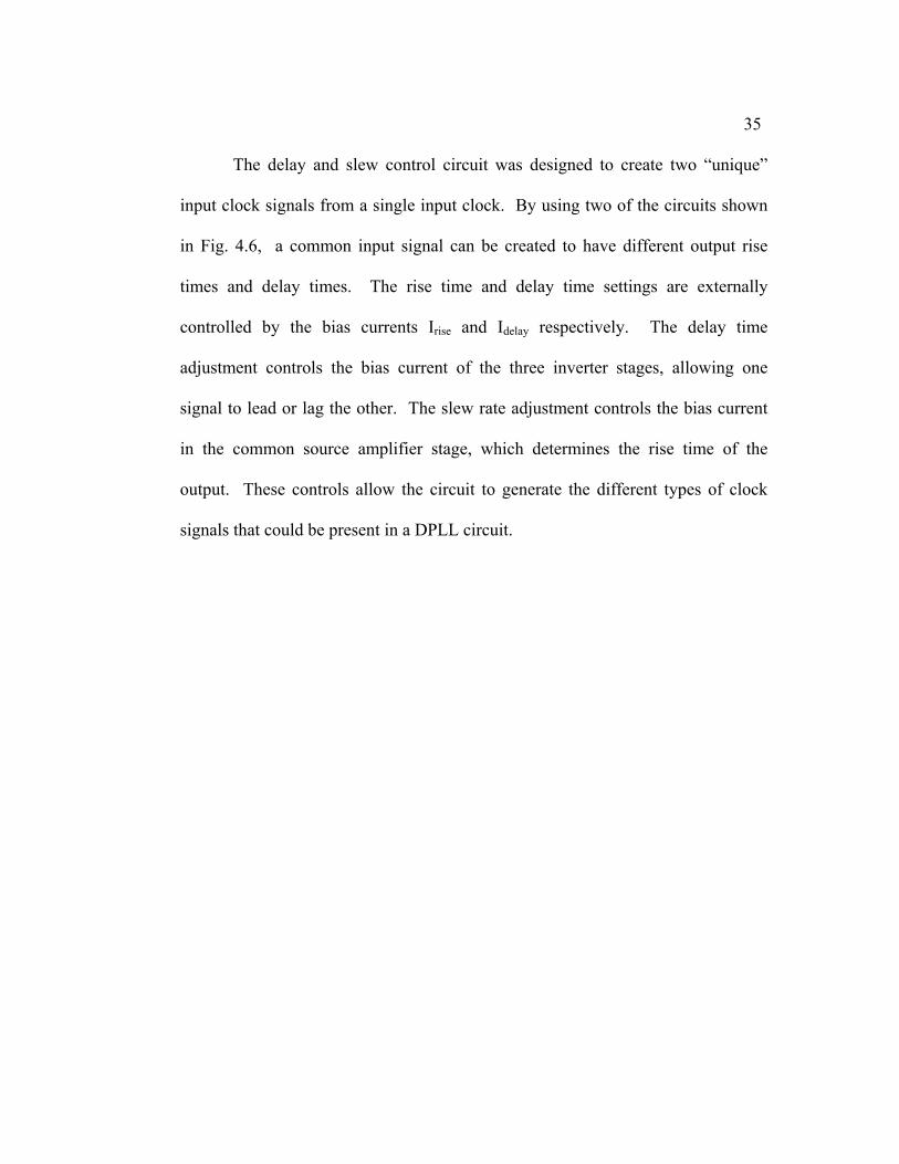
Figure 4.6. Delay and slew control circuit schematic.
VDD
Bias Bias
B ias Out
In I delay
Irise
35
The delay and slew control circuit was designed to create two “unique”
input clock signals from a single input clock. By using two of the circuits shown
in Fig. 4.6, a common input signal can be created to have different output rise
times and delay times. The rise time and delay time settings are externally
controlled by the bias currents Irise and Idelay respectively. The delay time
adjustment controls the bias current of the three inverter stages, allowing one
signal to lead or lag the other. The slew rate adjustment controls the bias current
in the common source amplifier stage, which determines the rise time of the
output. These controls allow the circuit to generate the different types of clock
signals that could be present in a DPLL circuit.
36
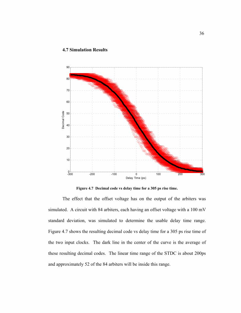
4.7 Simulation Results
-300 -200 -100 0 100 200 3000
10
20
30
40
50
60
70
80
90
Delay Time (ps)
Dec
imal
Cod
e
Figure 4.7 Decimal code vs delay time for a 305 ps rise time.
The effect that the offset voltage has on the output of the arbiters was
simulated. A circuit with 84 arbiters, each having an offset voltage with a 100 mV
standard deviation, was simulated to determine the usable delay time range.
Figure 4.7 shows the resulting decimal code vs delay time for a 305 ps rise time of
the two input clocks. The dark line in the center of the curve is the average of
these resulting decimal codes. The linear time range of the STDC is about 200ps
and approximately 52 of the 84 arbiters will be inside this range.
37
0 50 100 150 200 250 300 350 400 450-500
-400
-300
-200
-100
0
100
200
300
400
500
Current (uA)
Del
ay (p
s)
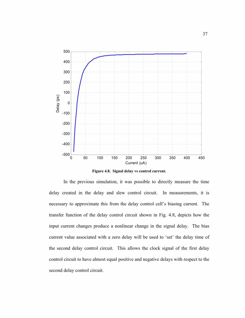
Figure 4.8. Signal delay vs control current.
In the previous simulation, it was possible to directly measure the time
delay created in the delay and slew control circuit. In measurements, it is
necessary to approximate this from the delay control cell’s biasing current. The
transfer function of the delay control circuit shown in Fig. 4.8, depicts how the
input current changes produce a nonlinear change in the signal delay. The bias
current value associated with a zero delay will be used to ‘set’ the delay time of
the second delay control circuit. This allows the clock signal of the first delay
control circuit to have almost equal positive and negative delays with respect to the
second delay control circuit.
38
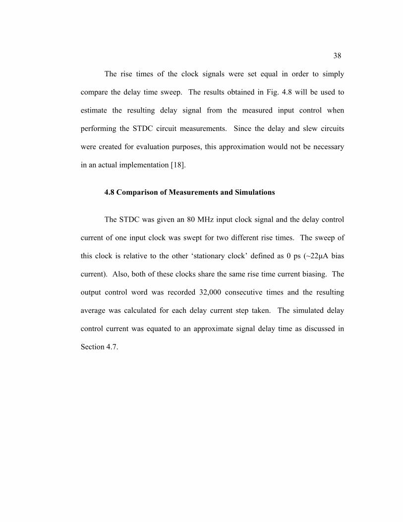
The rise times of the clock signals were set equal in order to simply
compare the delay time sweep. The results obtained in Fig. 4.8 will be used to
estimate the resulting delay signal from the measured input control when
performing the STDC circuit measurements. Since the delay and slew circuits
were created for evaluation purposes, this approximation would not be necessary
in an actual implementation [18].
4.8 Comparison of Measurements and Simulations
The STDC was given an 80 MHz input clock signal and the delay control
current of one input clock was swept for two different rise times. The sweep of
this clock is relative to the other ‘stationary clock’ defined as 0 ps (~22µA bias
current). Also, both of these clocks share the same rise time current biasing. The
output control word was recorded 32,000 consecutive times and the resulting
average was calculated for each delay current step taken. The simulated delay
control current was equated to an approximate signal delay time as discussed in
Section 4.7.
39
-300 -200 -100 0 100 200 3000
10
20
30
40
50
60
70
80
Simulation Mapped Delay Time (ps)
Ave
rage
Dec
imal
Cod
eChip #1Chip #2Chip #3Chip #4Simulated
Figure 4.9 Average decimal code output vs delay time.
Figure 4.9 shows the measured results of the STDC’s output as the delay
control is swept. The simulated average from Fig. 4.7 was also plotted for
comparison. As can be seen in the plot, about half of the arbiters are ‘tripped’
when there is zero delay time between the two clock signals. Since each of the
four measured chips shows similar characteristics, the offset voltage distribution
between the chips is also similar. The rise time of the measurements was
approximated to be 230 ps. Finally, the resolution of the STDC is about 25 times
smaller than the resolution of the TDC using an inverter chain.
40
-500 -400 -300 -200 -100 0 100 200 300 400 5000
10
20
30
40
50
60
70
80
Simulation Mapped Delay Time (ps)
Ave
rage
Dec
imal
Cod
eRise Time - 340psRise Time - 230ps
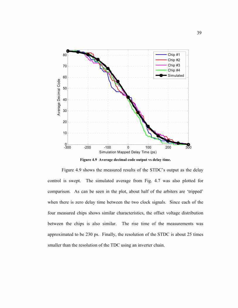
Figure 4.10 Decimal code output vs delay time. Figure 4.10 compares the STDC performance of one test circuit for 340ps
and 230ps rise time settings. The figure shows how the time measurement
window can be altered by simply changing the rise time of the input signals.
Also, the statistical offset voltage produced by the 84 arbiters is adequate for
measuring small time differences in the input signals. The good correlation
between the chips suggests that such a design could be used in mass production.
41
5. CONCLUSIONS
Typically, transistor mismatch is undesired in analog circuits because it
limits the circuit’s performance. However, the results shown in the previous
section demonstrate that mismatch can be used to improve the resolution of time
measurements. The achieved resolution of the STDC was less than an inverter’s
propagation time at the cost of additional circuitry involving the use of 84 arbiters
and their related hardware.
In the DPLL, the mismatch of the binary current sources in the DACs
created non-idealities in the DCAO tuning curve. This DAC would require
calibration of the elements in order to eliminate the current offsets that create the
poor INL/DNL performance. The recommendation of using a combination of
thermometer and binary weighted elements [12] would most likely reduce the
mismatch that is present.
Although the DPLL was able to lock, its performance was severely
limited. A possible cause is the noise coupling from the input/output buffers or
perhaps from the DCAO. The DCAO mismatch between the fine and coarse
DACs may have also limited the lock range of the DPLL.
For future designs, the following points are made to show potential areas
that can be improved.
• The input/output buffers should use their own power supply pins to
eliminate the possibility that their switching noise is coupling onto
the power supply rails.

42
• If the 0.35µm process is reused, the size of the buffers could be
reduced.
• For debugging purposes, it would be desirable to clear the value
stored in the integrator. The current design has no reset capability
and the integrator value is unknown at startup. This leads to a
repeatability issue since the DPLL does not always lock for the
same input conditions.
• The integrator’s gain value should be made programmable to test
several unity gain bandwidths.
• When open loop control of the DCAO is desired, the control word
should be programmed with a serial data stream rather than by
parallel bits. A serial shift register can store the DCAO control
word. Considering the fact that measuring the DCAO’s frequency
over all 12 bits would need to be automated, a serial input stream
would not add significantly to the design complexity. Also, this
would have allowed more package pins to be available for other
uses.
• The variable delay controls for the TDC used voltage signals for
biasing instead of current signals. Current signals should have
been used for biasing since they are less sensitive to noise.
• A calibration routine that eliminates arbiters with extremely large
offset voltages or those with offset voltages approximately equal to
43
others can be implemented. This calibration routine reduces the
hardware used while the DPLL is running at the cost of additional
setup hardware. By reducing the hardware, the STDC could
operate at higher speeds.
44
BIBLIOGRAPHY
[1] H. de Bellescize, "La reception synchrone," Onde Electrique, vol. 11, pp.
230-240, June 1932. [2] F. M. Gardner, “Charge-pump phase-locked loops,” IEEE Trans. Commun.,
vol. COM-28, pp. 1849-1858, Nov. 1980. [3] J. Maneatis, “Low-jitter process-independent DLL and PLL based on self-
bias techniques,” IEEE J. Solid-State Circuits, vol. 31, pp. 1723-1732, Dec. 1993.
[4] A. Marques, M. Steyaert, and W. Sansen, “Theory of PLL fractional-N
frequency synthesizers,” Wireless Networks 4, pp. 79-85, 1998. [5] A. Nemmani, “Design Techniques for Radiation Hardened Phase-Locked
Loops,” Master’s thesis, Oregon State University, Aug. 2005. [6] M. Vandepas, “Oscillators and Phase Locked Loops for Space Radiation
Environments,” Master’s thesis, Oregon State University, Aug. 2005. [7] R. B. Staszewski, S. Vemulapalli, P. Vallur, J. Wallberg, and P. Balsara,
“1.3 V 20 ps time-to-digital converter for frequency synthesis in 90-nm CMOS,” IEEE Trans. Circuits and Systems I, vol. 53, pp. 220-224, Mar. 2006.
[8] J. Lin, B. Haroun, T. Foo, J. Wang, B. Helmick, S. Randall, T. Mayhugh, C.
Barr, and J. Kirkpatrick, “ A PVT tolerant 0.18MHz to 600MHz self-calibrated digital PLL in 90nm CMOS process,” in ISSCC Dig. Tech. Papers, Feb. 2004, pp. 488-489.
[9] R. C. Walker, “Designing bang-bang PLLs for clock and data recovery in
serial data transmissions systems,” pp. 34-45, a chapter appearing in Phase-Locking in High-Performance Sytems - From Devices to Architectures (B. Razavi, editor). IEEE Press, 2003.
[10] J. Lee and B. Kim, “A low-noise fast-lock phase-locked loop with adaptive
bandwidth control,” IEEE J. Solid-State Circuits, vol. 35, pp. 1137-1145, Aug. 2000.
[11] P. K. Hanumolu, M. Brownlee, K. Mayaram, and U. Moon, “Analysis of
charge-pump phase-locked loops,” IEEE Trans. Circuits and Systems I, vol. 51, pp. 1665-1674, Sept. 2004.
45 [12] C. Lin and K. Bult, “A 10-b, 500-MSample/s CMOS DAC in 0.6 mm2,”
IEEE J. Solid-State Circuits, vol. 33, pp. 1948-1958, Dec. 1998. [13] V. Gutnik and A. Chandrakasan, “On-chip picosecond time measurement,”
in IEEE Symp. VLSI Circuits, Jun. 2000, pp. 52-53. [14] K. Ok, “A Stochastic Time-to-Digital Converter for Digital Phase-Locked
Loops,” Master’s thesis, Oregon State University, Aug. 2005. [15] B. Larson, “MOI5 Spice Model Specification.” Honeywell - Solid State
Electronics Center, 2001. [16] P. Drennan and C. McAndrew, “Understanding MOSFET mismatch for
analog design,” IEEE J. Solid-State Circuits, vol. 38, pp. 450-456, Mar. 2003.
[17] M. J. M. Pelgrom, C. J. Duinmaijer, and A. P. G. Welbers, “Matching
properties of MOS transistors,” IEEE J. Solid-State Circuits, vol. 24, pp. 1433-1440, Oct. 1989.
[18] V. Kratyuk, P. Hanumolu, K. Ok, K. Mayaram, and U. Moon, “A digital PLL
with a stochastic time-to-digital converter,” in IEEE Symp. VLSI Circuits, pp. 38-39, June 2006.
[19] B. Razavi, Design of Analog CMOS Integrated Circuits. New York:
McGraw Hill, 2001.
46
APPENDICES
47
Appendix A Additional IC and PCB Details
Statistical TDC Digital PLL
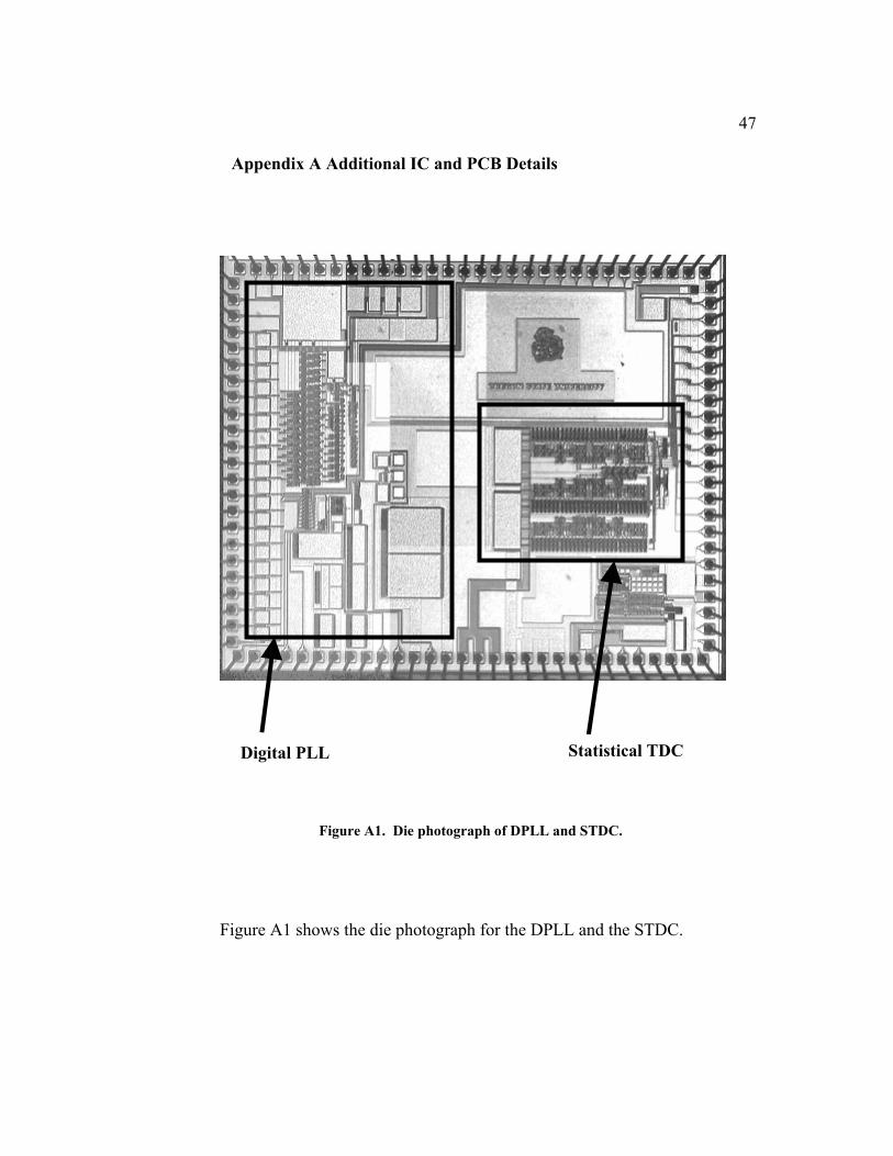
Figure A1. Die photograph of DPLL and STDC.
Figure A1 shows the die photograph for the DPLL and the STDC.
48
DIGITAL PLLStatistical TDC
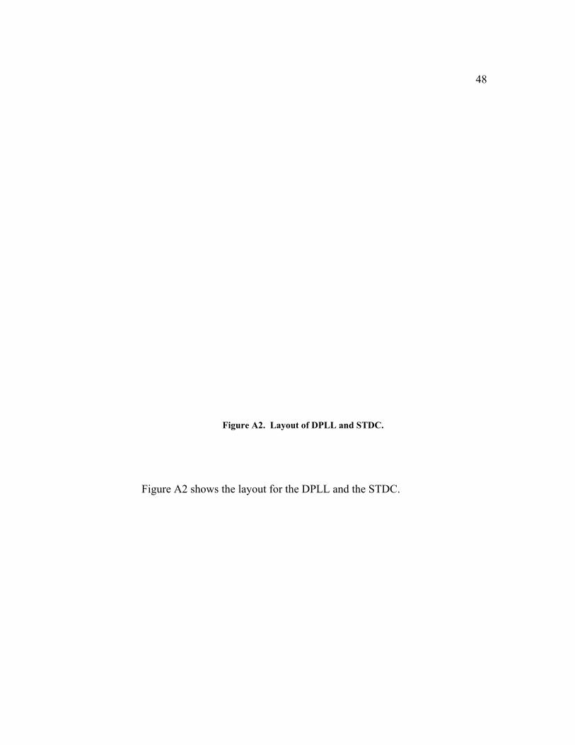
Figure A2. Layout of DPLL and STDC.
Figure A2 shows the layout for the DPLL and the STDC.
49
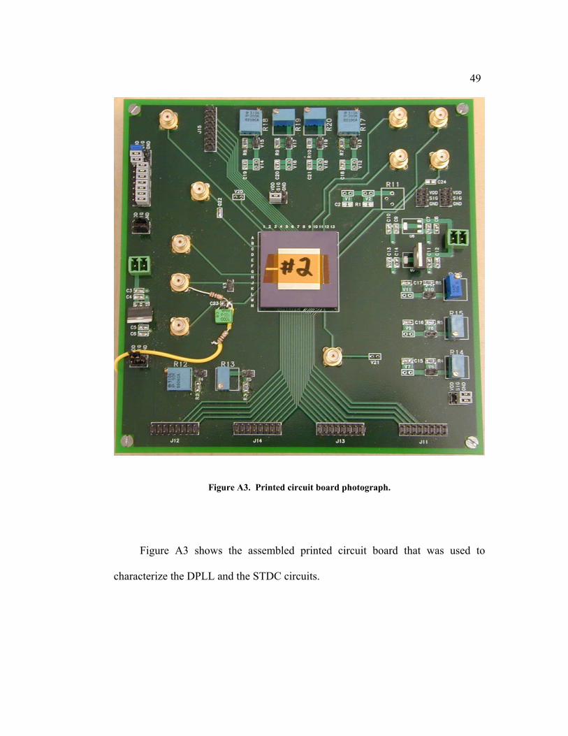
Figure A3. Printed circuit board photograph.
Figure A3 shows the assembled printed circuit board that was used to
characterize the DPLL and the STDC circuits.
50
Appendix B Additional Measurements
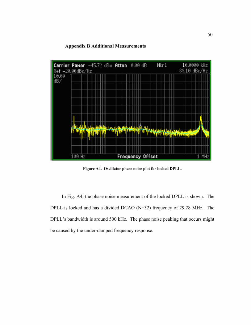
Figure A4. Oscillator phase noise plot for locked DPLL.
In Fig. A4, the phase noise measurement of the locked DPLL is shown. The
DPLL is locked and has a divided DCAO (N=32) frequency of 29.28 MHz. The
DPLL’s bandwidth is around 500 kHz. The phase noise peaking that occurs might
be caused by the under-damped frequency response.
51
0 100 200 300 400 500 600 700 800 900 1000650
700
750
800
850
900
950
1000
Decimal Codes
Freq
uenc
y (M
Hz)
MeasuredSimulated
Figure A5. DCAO tuning characteristic.
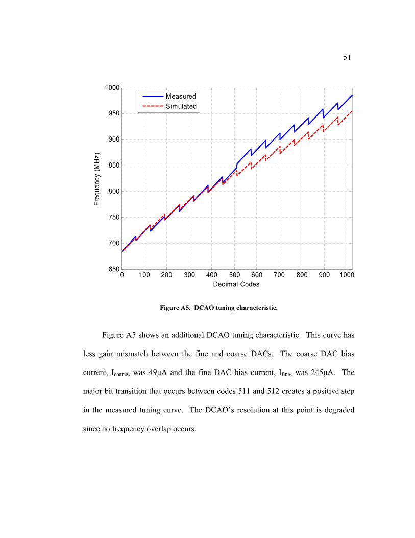
Figure A5 shows an additional DCAO tuning characteristic. This curve has
less gain mismatch between the fine and coarse DACs. The coarse DAC bias
current, Icoarse, was 49µA and the fine DAC bias current, Ifine, was 245µA. The
major bit transition that occurs between codes 511 and 512 creates a positive step
in the measured tuning curve. The DCAO’s resolution at this point is degraded
since no frequency overlap occurs.
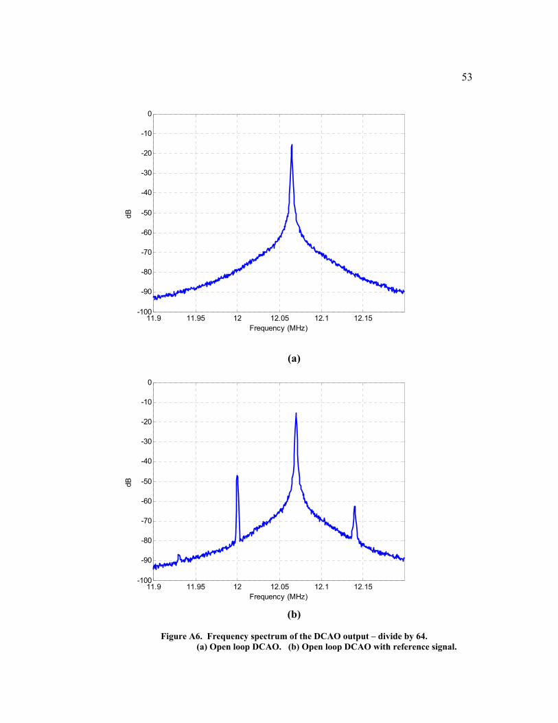
52 Figure A6 (a) shows the DCAO’s open loop frequency spectrum after the
divide-by-N circuit (where N = 64). Figure A6 (b) also shows the DCAO’s open
loop frequency spectrum with a 12.0 MHz reference signal being injected. The
coupling of the reference signal onto the DCAO’s divided output can be seen.
Both of the spectrum plots are an average of 100 measurements.
53
11.9 11.95 12 12.05 12.1 12.15-100
-90
-80
-70
-60
-50
-40
-30
-20
-10
0
dB
Frequency (MHz)
(a)
11.9 11.95 12 12.05 12.1 12.15-100
-90
-80
-70
-60
-50
-40
-30
-20
-10
0
dB
Frequency (MHz)
(b)
Figure A6. Frequency spectrum of the DCAO output – divide by 64. (a) Open loop DCAO. (b) Open loop DCAO with reference signal.
54
0 5 10 15 20 25 30 35 40 45-400
-200
0
200
400
Pha
se W
ord
Time (microseconds)
0 5 10 15 20 25 30 35 40 450
500
1000
1500
Time (microseconds)
CTR
L W
ord
Figure A7. Phase error and control signal with large reference signal vs time.
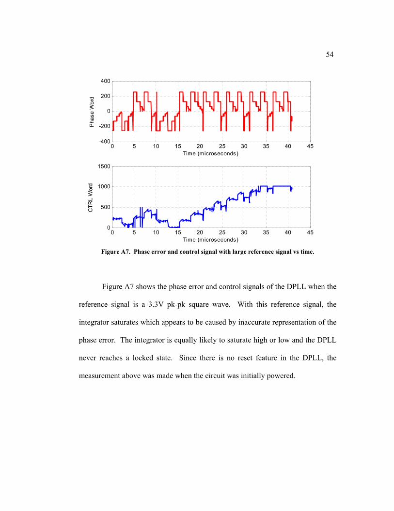
Figure A7 shows the phase error and control signals of the DPLL when the
reference signal is a 3.3V pk-pk square wave. With this reference signal, the
integrator saturates which appears to be caused by inaccurate representation of the
phase error. The integrator is equally likely to saturate high or low and the DPLL
never reaches a locked state. Since there is no reset feature in the DPLL, the
measurement above was made when the circuit was initially powered.
55
0 0.5 1 1.5 2 2.5 3-4
-2
0
2
4
Pha
se W
ord
Time (microseconds)
0 0.5 1 1.5 2 2.5 30
20
40
60
80
100
Time (microseconds)
STD
C C
ode
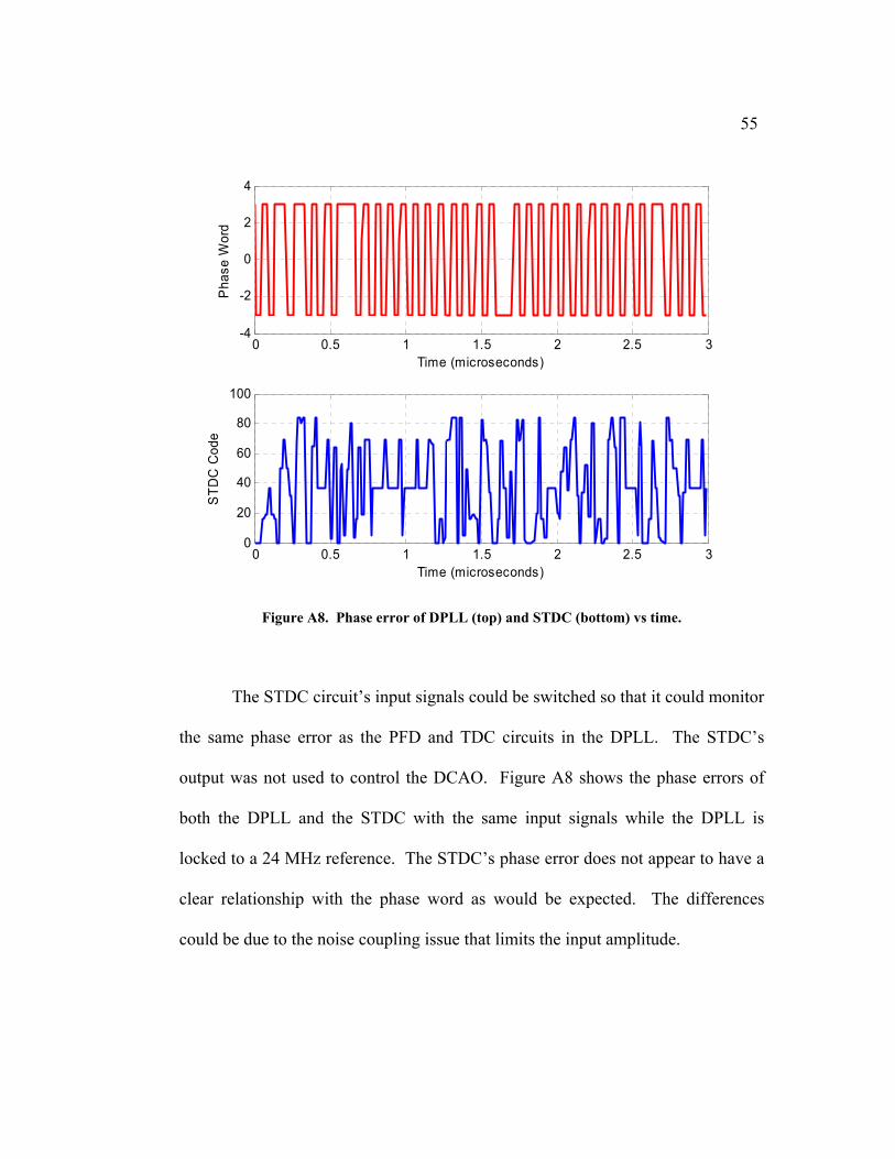
Figure A8. Phase error of DPLL (top) and STDC (bottom) vs time. The STDC circuit’s input signals could be switched so that it could monitor
the same phase error as the PFD and TDC circuits in the DPLL. The STDC’s
output was not used to control the DCAO. Figure A8 shows the phase errors of
both the DPLL and the STDC with the same input signals while the DPLL is
locked to a 24 MHz reference. The STDC’s phase error does not appear to have a
clear relationship with the phase word as would be expected. The differences
could be due to the noise coupling issue that limits the input amplitude.