aalto-1 radmon experiment interface document-part … radmon eid... · aalto-1 radmon experiment...
TRANSCRIPT

Doc. No. A1-RAD-IF-03-v2-DRAFT
RADMON Issue DRAFT
RADMON Experiment Interface Document-Part B Date:17.03.2014
Page: 1 (27)
Aalto-1
Aalto-1
RADMON Experiment Interface Document-Part B
Name Signature Date
Prepared by J. Peltonen 14.03.2014
17.03.2014
Checked by R. Vainio 15.03.2015
Approved by
DISTRIBUTION
Name Organisation
Aalto-1 Team
CHANGE LOG
Date Issue Rev. Pages Reason for change
29.10.2013 03 v1-Draft New document for CDR replacing all earlier EID-B versions
14.03.2014 (JP)
15.03.2014 (RV)
17.03.2014 (JP)
03
03
03
v2-Draft
v2-Draft
v2-Draft
1-27
Corrections related to RIDs before the CDR
Added operational modes
Clarifications to the communication section
Resolution/clarity of some images
Scientific part corrections. General document check
Added table of content. Changed some heading levels for
readability. Further clarifications to the text.

Doc. No. A1-RAD-IF-03-v2-DRAFT
RADMON Issue DRAFT
RADMON Experiment Interface Document-Part B Date:17.03.2014
Page: 2 (27)
Aalto-1
Contents
1 Introduction .............................................................................................................................................. 3
1.1 Scope ................................................................................................................................................. 3
1.2 Applicable Documents ....................................................................................................................... 3
1.3 Reference Documents ....................................................................................................................... 3
1.4 Abbreviations and Acronyms............................................................................................................. 3
2 Mechanical Interface ................................................................................................................................ 4
2.1 Coordinate System and Mechanical Structure .................................................................................. 4
2.2 Mass Budget ...................................................................................................................................... 5
2.3 Center of Mass and Moments of Inertia ........................................................................................... 6
2.4 Mechanical Interface to the Spacecraft ............................................................................................ 6
3 Electrical Interface .................................................................................................................................... 9
3.1 General Description of RADMON Electronics .................................................................................... 9
3.2 Subunits Interfacing (RADMON Bus) ................................................................................................. 9
3.3 Aalto-1 Bus Interfacing .................................................................................................................... 11
3.4 Grounding ........................................................................................................................................ 12
3.5 Communication Interfaces .............................................................................................................. 12
3.5.1 Interfacing, Bits and Bytes ....................................................................................................... 13
3.6 Power Interface ............................................................................................................................... 14
3.6.1 Power Modes and Currents ..................................................................................................... 15
3.7 Electromagnetic Interface ............................................................................................................... 15
4 Software Interface, Data Transfers and Commands ............................................................................... 17
4.1 Data Protocols ................................................................................................................................. 17
4.2 RADMON Commanding ................................................................................................................... 17
4.3 Data and Housekeeping Read Rates ................................................................................................ 20
4.4 Data/Housekeeping Content ........................................................................................................... 20
4.5 Housekeeping Measurements ......................................................................................................... 20
5 RADMON Operational Modes ................................................................................................................. 22
6 Thermal Interface ................................................................................................................................... 23
6.1 Expected Dynamical Thermal Load over Experiment Operation Cycle ........................................... 23
6.2 Acceptable Operational and Stand-by Temperature Ranges .......................................................... 23
6.3 Expected Components for Cooling/Heating .................................................................................... 23
7 Ground Segment ..................................................................................................................................... 24
7.1 Ground support equipment ............................................................................................................ 24
7.2 Communication and Data Delivery .................................................................................................. 24
8 Scientific Experiment .............................................................................................................................. 25
8.1 Observed Data and Mission Objectives ........................................................................................... 25
8.2 Experiment Cycle Description.......................................................................................................... 25
8.3 Dynamic Power Budget ................................................................................................................... 27
8.4 Dynamic Data Budget ...................................................................................................................... 27
8.5 Attitude Control and Determination Requirements ....................................................................... 27
8.6 Positioning Requirements ............................................................................................................... 27

Doc. No. A1-RAD-IF-03-v2-DRAFT
RADMON Issue DRAFT
RADMON Experiment Interface Document-Part B Date:17.03.2014
Page: 3 (27)
Aalto-1
1 Introduction
1.1 Scope
This document provides the Part B of the Experiment Interface Document for RADMON, the radiation
monitor for the Aalto-1 satellite. A new document version IF-03 was created for the Critical Design Review.
1.2 Applicable Documents
Ref. Document Name Document Reference Issue
A1 Experiment Interface Document (Part A) A1-SYS-EID-01 v7
1.3 Reference Documents
Ref. Document Name Document Reference Issue
R1 Mechanical Drawings for RADMON A1-RAD-DW-01 Draft
R2 Aalto-1 OBC –
Payload Communication Protocol Definitions
and Details
A1-OBH-DS-03-v3 10.7.2013
1.4 Abbreviations and Acronyms
EMC Electro Magnetic Cleanliness
HK House Keeping (measurements)
I2C Inter- IC bus
LVDS Low Voltage Differential Signaling
PCB Printed circuit board
PSU Power Supply Unit
RADMON Radiation Monitor for Aalto-1 satellite

Doc. No. A1-RAD-IF-03-v2-DRAFT
RADMON Issue DRAFT
RADMON Experiment Interface Document-Part B Date:17.03.2014
Page: 4 (27)
Aalto-1
2 Mechanical Interface
2.1 Coordinate System and Mechanical Structure
The S/C coordinate system is defined in [A1] and depicted in Fig. 1. RADMON is placed so that its field-of-
view is through the –Z panel. The figure gives a sketch of the RADMON Unit and its main parts. A
summary of the mechanical structure is given below. For a more detailed description of the mechanical
design, see [R1].
RADMON has a mechanical structure consisting of five subunits (Figure 1):
• Detector Unit: quasi-cubical, 30×30×27.2 mm³ (TBC) with two extruding Board-to-Wire connectors
• Power Supply Unit (PSU) Board: one-sided CubeSat-kit-compliant PCB (90.17×95.89 mm²) with
PC104 bus connector (1×SAMTEC ESQ-126-39-G-D) and another stack-through-connector
SAMTEC ESQ-126-37-G-D to the Digital Electronics Board
• Digital Electronics Board: two-sided CubeSat-kit-compliant PCB (90.17×95.89 mm²) with a stack-
through-connector SAMTEC SSQ-126-22-G-D to the PSU Board and to the Analog Electronics
Board
• Analog Electronics Board: two-sided CubeSat-kit-compliant PCB (90.17×95.89 mm²) with a stack-
through-connector SAMTEC SSQ-126-22-G-D to the Digital Electronics Board
• Top Frame: Al structure providing support for the detector and the upper mechanical interface to the
spacecraft.
The main outer dimensions of RADMON are:
Figure 1. Radmon mechanical structure

Doc. No. A1-RAD-IF-03-v2-DRAFT
RADMON Issue DRAFT
RADMON Experiment Interface Document-Part B Date:17.03.2014
Page: 5 (27)
Aalto-1
o width (X-direction) 90.17 mm
o height (Y-direction) 40.00 mm
o depth (Z-direction) 95.89 mm
The Detector Unit extrudes outside this envelope by 7 mm (TBC) towards the –Z-direction, providing it with
a view to space. The cross-section of the extruding part (in XY plane) is 30×30 mm² and positioned 1 mm
(TBC) below the upper plane of the unit in the Y direction and centered in the X direction.
The RADMON will be attached to the Aalto-1 short-stack with four 3 mm crews at the corners.
The detector of RADMON will be also attached from below with two 3 mm screws and spacers to the Al-
support on the PSU board. And from above with two 3mm screws to the support frame and with two 3 mm
(TBC) screws to the short stack support plate.
Note that the screw heads will be extruding the main envelope below and possibly from the detector top side
at the frame and short stack connection (TBC). In addition, the 52 pins of the Board-to-Board through
connector between the PSU Board and the Digital Board will extrude the bottom plane by ~1 mm (TBC).
Thus, Plasma Brake should not assume a completely flat lower surface of RADMON.
The boards will be stacked using the 52-pin stack-through connectors. In addition, they will be mated by
(M3) male-female stainless steel standoffs in the corners (see http://www.unicorpinc.
com/metric_3.2mm_maletofemale.htm ). If needed, a thin PTFE (teflon) insulator will be added between the
standoffs and the PCB boards (TBC).
The distances between the PCB boards are
• PSU Board -Digital Board 14.6 mm (bottom to bottom)
• Digital Board – Analog Board 12.1 mm (bottom to bottom)
• Analog Board – Upper Frame 13.3 mm (bottom to top)
The positions of the screw holes are determined by the CubeSat-kit PCB dimensions. The Top Frame has
screw holes with 3-mm thread at correct positions for the male end of the standoffs between the Analog
Electronics Board and the Digital Electronics Board.
2.2 Mass Budget
The mass breakdown of RADMON at subunit level is presented in Table 1. The mass of the PCBs is
estimated using the thickness 0.16 cm, the outer dimensions 9.017×9.589 cm² and FR-4 mass density of 1.85
g cm⁻³. This gives a base mass of 23.6/25.6 g for cards with/without the (2.1×3.2 cm²) cutout for the
Detector Unit. PC-104 style connectors are assumed to weigh 8 g / 52 pins. The Detector Unit mass is
estimated as follows: 135 g for the outer brass parts (assuming density 8.7 g cm⁻³), 5 g for the CsI crystal and
10 g for the rest (consisting mainly of plastic).
Currently the mass budget includes some reserve for addition of copper between the PCB boards and for
changing TBD plastic parts to ceramic. The first proto model PCB boards weighted ~150 g (measured
17.10.2013: PSU1 56g, Dig 44g, Ana 44g and Det 144g,). The weight will increase some for the next models
but the total weight will stay in the given limits.
A more detailed breakdown of RADMON mass is presented in [R1].

Doc. No. A1-RAD-IF-03-v2-DRAFT
RADMON Issue DRAFT
RADMON Experiment Interface Document-Part B Date:17.03.2014
Page: 6 (27)
Aalto-1
Table 1. Mass breakdown for RADMON. All numbers TBC. Margin is 20% of the estimated
mass.
Subunit Mass (g) Margin (g) Mass with margin (g)
Detector Unit 150 30 180
PSU Board + Connectors 80 16 96
Digital Electronics Board + Connector 70 14 84
Analog Electronics Board + Connector 60 12 72
Top Frame 25 5 30
Standoffs, screws, spacers 30 6 24
Total 415 83 498
2.3 Center of Mass and Moments of Inertia
Will be determined by measurement (CM) and using the CAD model.
2.4 Mechanical Interface to the Spacecraft
The mechanical interface to the spacecraft and the outer dimensions of RADMON are compliant with [A1].
The mechanical interface between the RADMON stack and the spacecraft is achieved from above through
the screw holes with 3-mm thread through the corners of the Top Frame (see Fig. 2). Their positions are
determined according to the standard hole positions of a CubeSat-kit PCB, as required in [A1].
The orientation of the male-female connectors is such that RADMON has male interfaces towards the
Plasma Brake.

Doc. No. A1-RAD-IF-03-v2-DRAFT
RADMON Issue DRAFT
RADMON Experiment Interface Document-Part B Date:17.03.2014
Page: 7 (27)
Aalto-1
Figure 2. RADMON Top Frame

Doc. No. A1-RAD-IF-03-v2-DRAFT
RADMON Issue DRAFT
RADMON Experiment Interface Document-Part B Date:17.03.2014
Page: 8 (27)
Aalto-1
The protruding part of the Detector Unit has two M3 (TBC) screw holes in TBD positions facing the short-
stack support plate (see [A1]) on top of RADMON, to allow further support to the heavy detector unit. Using
these holes, the Detector Unit shall be fixed to the short stack support plate.
Figure 3. RADMON PSU Board viewed from above (top) and from the +X side
(bottom).

Doc. No. A1-RAD-IF-03-v2-DRAFT
RADMON Issue DRAFT
RADMON Experiment Interface Document-Part B Date:17.03.2014
Page: 9 (27)
Aalto-1
3 Electrical Interface
3.1 General Description of RADMON Electronics
Electrically, RADMON consists of four subunits:
• Detector Unit
• Analog Electronics Board
• Digital Electronics Board
• PSU Board
An overview of the electrical interfaces between the four subunits and the S/C is depicted in Fig. 4. The
spacecraft PC-104 bus (sBus) shall be implemented as in [A1]. Inside RADMON, the sBus extends only to
the PSU Board. From there on, the power lines and inter-board communication are handled via the 52-pin
(TBC) RADMON bus. See [R2] for more information.
3.2 Subunits Interfacing (RADMON Bus)
The Aalto-1 Short Stack communication signals go from the RADMON Power board the Digital board via
the RADMON internal bus. RADMON internal bus connections are therefore summarized also here.
The Detector Unit is connected to the Analog Board via two harnesses, one for each detector. Signals carried
by the harnesses are bias (about –50 V) and ground. The Si detector has a guard ring, which has to be biased
as well. The harness for the Si detector needs three signal wires and the one for the photodiode needs two.
Figure 4. Overview of RADMON electrical interfaces. Spacecraft Bus is terminated at the
PSU Board. All signal and power lines between the RADMON Boards are via the RADMON
bus consisting of a 52-pin (TBC) stack-through connector. The Detector Unit is connected to
the Analog Board via two harnesses, one for each detector.

Doc. No. A1-RAD-IF-03-v2-DRAFT
RADMON Issue DRAFT
RADMON Experiment Interface Document-Part B Date:17.03.2014
Page: 10 (27)
Aalto-1
Internally RADMON communicates through 52-pin bus. The internal bus pin layout and
signals are shown in Figure 5.
Figure 5. RADMON internal bus pin order
Remarks From-To Bus Signal Bus Signal From-To Remarks
Scintillator Ana-Dig SCINT_B11 1 2 SCINT_B10 Ana-Dig Scintillator
Scintillator Ana-Dig SCINT_B9 3 4 SCINT_B8 Ana-Dig Scintillator
Scintillator Ana-Dig SCINT_B7 5 6 SCINT_B6 Ana-Dig Scintillator
Scintillator Ana-Dig SCINT_B5 7 8 SCINT_B4 Ana-Dig Scintillator
Scintillator Ana-Dig SCINT_B3 9 10 SCINT_B2 Ana-Dig Scintillator
Scintillator Ana-Dig SCINT_B1 11 12 SCINT_B0 Ana-Dig Scintillator
Semicond Ana-Dig SEMI_B11 13 14 SEMI_B10 Ana-Dig Semicond
Semicond Ana-Dig SEMI_B9 15 16 SEMI_B8 Ana-Dig Semicond
Semicond Ana-Dig SEMI_B7 17 18 SEMI_B6 Ana-Dig Semicond
Semicond Ana-Dig SEMI_B5 19 20 SEMI_B4 Ana-Dig Semicond
Semicond Ana-Dig SEMI_B3 21 22 SEMI_B2 Ana-Dig Semicond
Semicond Ana-Dig SEMI_B1 23 24 SEMI_B0 Ana-Dig Semicond
GND 25 26 ANA_CS Dig-Bus Ana FF-Chip sel
CLK to Ana Dig-Ana ANA_CLOCK 27 28 HK_CLOCK Dig-Bus HK-Clock to all
GND 29 30 HK_DIN Bus-Dig
HK-DataIn to
FPGA
HK-Data Out Dig-Bus HK_DOUT 31 32 HK_CS1 Dig-Bus HK-Circuit CS
HK-Circuit CS Dig-Bus HK_CS2 33 34 HK_CS3 Dig-Bus HK-Circuit CS
LVDS
Communication
Dig-(PSU)-
Aalto LVDS_MISO_POS 35 36 LVDS_MISO_NEG
Dig-(PSU)-
Aalto
LVDS
Communication
LVDS
Communication
Aalto-(PSU)-
Dig LVDS_MOSI_POS 37 38 LVDS_MOSI_NEG
Aalto-(PSU)-
Dig
LVDS
Communication
I2C
Communication Aalto-PSU-Dig I2C_CLK_A 39 40 I”C_DATA_A
Bidirectional
Aalto-(PSU)-
I2C
Communication
NC 41 42 VREF Dig-Ana Ref 4.1 V
Power PSU-Dig +1.2V 43 44 +2.5V PSU-Dig Power
Power PSU-Dig +1.8V 45 46 -6V PSU-Ana Power
Power PSU-Dig/Ana +3.3V 47 48 +6V PSU-Ana Power
Bias on/off
Clock Dig-Ana BIAS_CLOCK 49 50 +12V PSU-Ana Power
GND 51 52 GND
HeaderRadmon Bus Signal Radmon Bus Signal

Doc. No. A1-RAD-IF-03-v2-DRAFT
RADMON Issue DRAFT
RADMON Experiment Interface Document-Part B Date:17.03.2014
Page: 11 (27)
Aalto-1
3.3 Aalto-1 Bus Interfacing
The Aalto-1 short stack signals used by RADMON (and the corresponding RADMON/PSU signals) are
shown in Fig 6.
Figure 6. RADMON short stack bus signals and pins
Remarks In/Out PSU Signal PSU Signal In/Out Remarks
Radmon LVDS Master
out, slave in+ In
LVDS_MOSI_PO
S RAD_LVDS_MOSI+ 1 2 RAD_LVDS_MOSI-
LVDS_MOSI_NE
G In
Radmon
LVDS
Master out,
Radmon LVDS Master
in, slave out+ Out
LVDS_MISO_PO
S RAD_LVDS_MISO+ 3 4 RAD_LVDS_MISO-
LVDS_MISO_NE
G Out
Radmon
LVDS
Master in,
Ground connection GND GND_1-5 5 6 GND_1-6 GND
Ground
connection
NC Reserved Aalto 7 8 Reserved Aalto NC
NC Reserved Aalto 9 10 Reserved Aalto NC
NC Reserved Aalto 11 12 Reserved Aalto NC
NC Reserved Aalto 13 14 Reserved Aalto NC
NC Reserved Aalto 15 16 Reserved Aalto NC
Radmon +12V power
line +12V_ABUS +12V RAD 17 18 +5V RAD +5V_ABUS
Radmon
+5V power
line
NC Reserved Aalto 19 20 Reserved Aalto NC
NC Reserved Aalto 21 22 Reserved Aalto NC
NC Reserved Aalto 23 24 Reserved Aalto NC
Ground connection GND GND_1-25 25 26 Reserved Aalto NC
NC Reserved Aalto 27 28 Reserved Aalto NC
NC Reserved Aalto 29 30 Reserved Aalto NC
NC Reserved Aalto 31 32 Reserved Aalto NC
Ground connection GND GND_1-33 33 34 GND_1-34 GND
Ground
connection
NC Reserved Aalto 35 36 Reserved Aalto NC
NC Reserved Aalto 37 38 Reserved Aalto NC
Ground connection GND GND_1-39 39 40 GND_1-40 GND
Ground
connection
I2C data In/Out I2C_DATA_A I2C_PRI DATA 41 42 I2C_PRI DATA I2C_DATA_A In/Out I2C data
I2C clock In I2C_CLK_A I2C_PRI CLK 43 44 I2C_PRI CLK I2C_CLK_A In I2C clock
NC Reserved Aalto 45 46 Reserved Aalto NC
NC Reserved Aalto 47 48 Reserved Aalto NC
NC Reserved Aalto 49 50 Reserved Aalto NC
NC Reserved Aalto 51 52 Reserved Aalto NC
Communication
Power
Radmon Signal Aalto Radmon Signal
Short Stack Header 2: Outer Header

Doc. No. A1-RAD-IF-03-v2-DRAFT
RADMON Issue DRAFT
RADMON Experiment Interface Document-Part B Date:17.03.2014
Page: 12 (27)
Aalto-1
3.4 Grounding
The RADMON detector unit enclosure or detector box is grounded directly to the spacecraft hull by
conductive screws. Sensor ground is connected to the signal ground near the amplifiers of the analog board
and further to the RADMON power/digital ground. A single common digital/power ground is used at the
digital card. The power ground origin is at the PSU board, near the power converters. At PSU, there is a
possibility to connect the chassis to the common RADMON ground at the PSU. Filtering is used at the
chassis connections to isolate the PCBs from noise sources of chassis. The details of this filter are TBD. A
reservation for a resistor in parallel with a capacitor has been made to the layout of PSU board in the
engineering model. Note that the Short Stack bus ground wires all connect at the RADMON interface. If
these grounds do not connect to common plane there is a loop possibility. At least two of these ground pins
should be in use at RADMON for connection reliability. The principle of RADMON grounding is shown in
Figure 7.
Figure 7. Principle of the electrical grounding of RADMON instrument (TBC).
3.5 Communication Interfaces
RADMON communicates with the S/C using
• Asynchronous Low Voltage Differential Signaling (LVDS) and
• Synchronous I2C-bus (Inter-IC) communication.
There is dedicated serial LVDS interface for RADMON, differential inputs terminated with 100 Ohm
resistor. The I2C bus is shared between other payloads and sensors. The pull-up resistors of I2C (2K2 Ohm)
and the serial resistors (47 Ohm) can be implemented or left out (TBC).
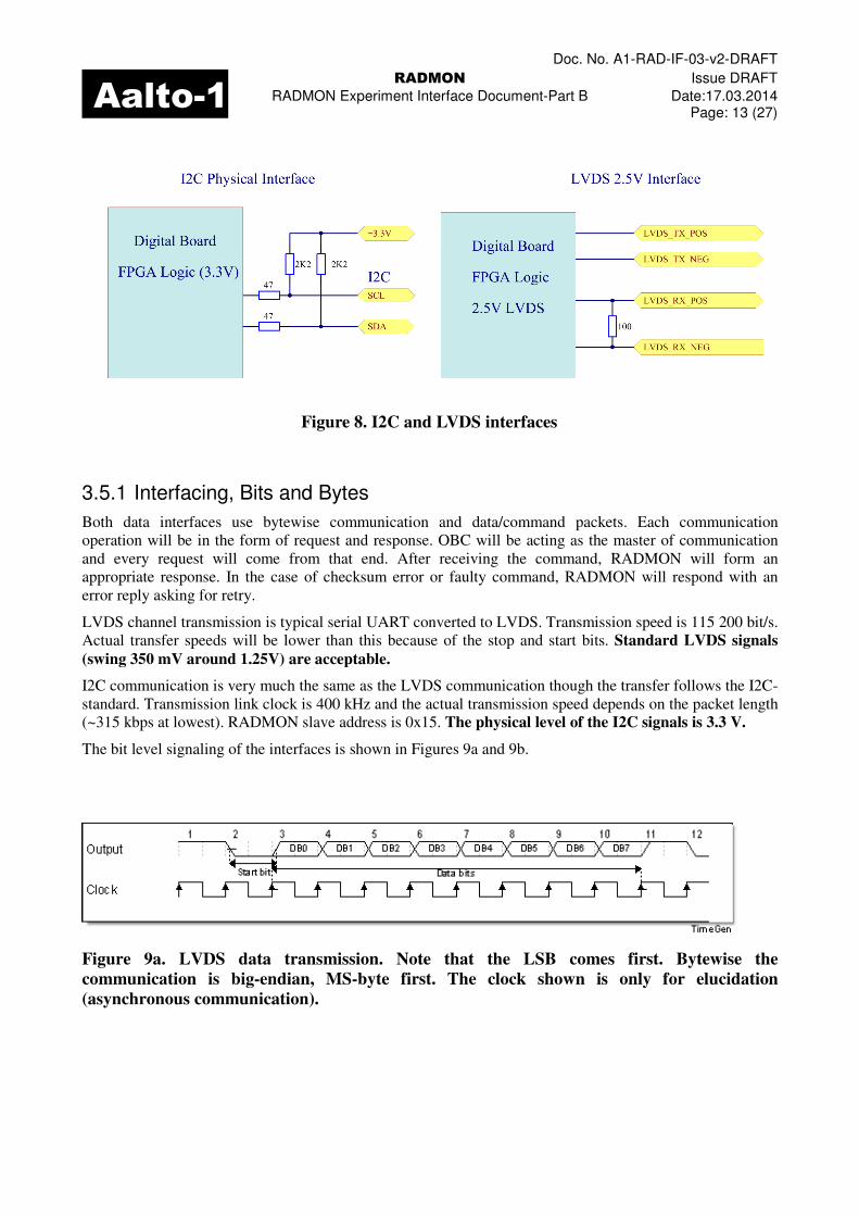
The physical interfaces are shown in Figure 8. .
Doc. No. A1-RAD-IF-03-v2-DRAFT
RADMON Issue DRAFT
RADMON Experiment Interface Document-Part B Date:17.03.2014
Page: 13 (27)
Aalto-1
Figure 8. I2C and LVDS interfaces
3.5.1 Interfacing, Bits and Bytes
Both data interfaces use bytewise communication and data/command packets. Each communication
operation will be in the form of request and response. OBC will be acting as the master of communication
and every request will come from that end. After receiving the command, RADMON will form an
appropriate response. In the case of checksum error or faulty command, RADMON will respond with an
error reply asking for retry.
LVDS channel transmission is typical serial UART converted to LVDS. Transmission speed is 115 200 bit/s.
Actual transfer speeds will be lower than this because of the stop and start bits. Standard LVDS signals
(swing 350 mV around 1.25V) are acceptable.
I2C communication is very much the same as the LVDS communication though the transfer follows the I2C-
standard. Transmission link clock is 400 kHz and the actual transmission speed depends on the packet length
(~315 kbps at lowest). RADMON slave address is 0x15. The physical level of the I2C signals is 3.3 V.
The bit level signaling of the interfaces is shown in Figures 9a and 9b.
Figure 9a. LVDS data transmission. Note that the LSB comes first. Bytewise the
communication is big-endian, MS-byte first. The clock shown is only for elucidation
(asynchronous communication).

Doc. No. A1-RAD-IF-03-v2-DRAFT
RADMON Issue DRAFT
RADMON Experiment Interface Document-Part B Date:17.03.2014
Page: 14 (27)
Aalto-1
Figure 9b. I2C data transmission. Note that MSB comes first in contrary to the LVDS
transmission.
The details of the packet formats are given in document [R2]. A shortened description of packets and
commanding is given also in Section 4.
3.6 Power Interface
RADMON uses S/C the +12V and +5V lines of the S/C power bus. The principle of the power connections
is shown in Fig. 10.
The power pins of Aalto-1 short stack were given in Figure 6.
Figure 10. Principle of the RADMON power connections, triggering the killswitch located at
the Aalto PSU cuts the RADMON +5V line. The RADMON +5V line then triggers an
internal switch of RADMON PSU cutting the +12V line. RADMON can tolerate any
switching order, however is preferred that the +12V input is ready when +5V is switched on.

Doc. No. A1-RAD-IF-03-v2-DRAFT
RADMON Issue DRAFT
RADMON Experiment Interface Document-Part B Date:17.03.2014
Page: 15 (27)
Aalto-1
3.6.1 Powers and Inrush Currents
RADMON has two power modes: on and off. The power consumption of RADMON is given in
Table 2.
Table 2 Power consumption and inrush currents of RADMON (TBC)
NODE Off
On
(Measurement
and Calibration
modes similar)
Inrush currents when
switched on REMARKS
+12VRAD 0 0.03A
~1 A peak, duration
~100 us. Less than 0.5A
averaged over 2 ms.
94 uF tantalum+
small ceramic at
input.
1.5 Ohm resistor
in series and then
overload
protection circuits.
+5VRAD 0 0.22 A
~0.6 A, duration ~1 ms
FPGA logic is
unfinished and this
power inrush value is
preliminary. We don’t
expect significant
change
94 uF tantalum +
small ceramic
at input
1 Ohm resistor in
series and then
overload
protection circuits.
3.7 Electromagnetic Interface
RADMON shall comply with the EMC-requirements of Aalto as given in [TBD] document. RAD-
MON uses only low power and low voltage electronics so it is believed it will not generate consid-
erable EM-noise.
The foreseen sources of electromagnetic radiation in Radmon are summarized in Table 3.
Doc. No. A1-RAD-IF-03-v2-DRAFT
RADMON Issue DRAFT
RADMON Experiment Interface Document-Part B Date:17.03.2014
Page: 16 (27)
Aalto-1
Table 3. EM noise sources of Radmon
Power supplies: ~500 kHz (+6.8V/60 mA peak)
~500 kHz (-6.8V/60 mA peak)
2.25 MHz fixed (digital voltages/0.8 A peak at start)
200 kHz fixed (+-6.8 V/50 mA peak)
FPGA and other logic:
Oscillator frequency 40 MHz
FPGA clock frequency 10 MHz
ADC conversion 10 MHZ
Communication I2C CLOCK 400 kHz
LVDS 111.5 kHz
The results of the following instrument EM tests will be made available:
• Emission measurements (radiation caused by RADMON)
o Conductive 150 kHz - 30 MHz
o Radiative 30 MHz - 1 GHz
• Behavior in RF radiation field (RADMON influenced by the field)
o Radiated RF field 80 MHz - 1 GHz
o Conductive RF field 0.15 - 80 MHz
The tests will be carried out at the EMC tests laboratory of Turku University of Applied Sciences.

Doc. No. A1-RAD-IF-03-v2-DRAFT
RADMON Issue DRAFT
RADMON Experiment Interface Document-Part B Date:17.03.2014
Page: 17 (27)
Aalto-1
4 Software Interface, Data Transfers and Commands
4.1 Data Protocols
The commands used in the protocol are 4-257 bytes wide. This range comes from the length field being one
byte that determines the packet length excluding checksum portion. The commands are designated to each
payload from the range of different commands. 8-bit command identifier gives us a range of 256 commands,
some of which are same for all payloads. Command structure is presented Figure 9. Communication between
RADMON and the OBC happens with this protocol. In addition to RADMON, other payloads will use the
same scheme as well.
Figure 9. Payload command packet according to the protocol
4.2 RADMON Commanding
Overview of the RADMON commanding is presented in Table 3. More details of the communica-
tion are given in [R2].

Doc. No. A1-RAD-IF-03-v2-DRAFT
RADMON Issue DRAFT
RADMON Experiment Interface Document-Part B Date:17.03.2014
Page: 18 (27)
Aalto-1
Table 4. RADMON commanding. Radmon will response sending the above specified data
package to OBS. The response ACK/ERR in the table refers to the content of the status field:
0x00= ACK, 0x01-0xFF error codes (TBD). On powering RADMON will automatically go to
the measurement mode.
Generic commands
Command name Function
Command pre-
requisite Hex value Response
Status Ask for house-
keeping data
Response possible
1 second from the
power switching
0x01 Housekeep-
ing data
On Turns payload
ON. Not used
by RADMON
Response possible
1 second from the
power switching
0x02 ACK/ERR
Off Command not
used. For
shutdown,
switch powers
OFF
0x03 ACK/ERR
Standby Same as ON.
Not used by
RADMON.
Response possible
1 second after the
power switching
0x04 ACK/ERR
Reset Resets payload
internal state
Further com-
mands possible 1
second from the
Reset command
0x05 ACK/ERR
RADMON specific commands 0x51 - 0x79
Command name Function Command pre-
requisite
Hex value Data accom-
panied
Response
Calibration The collection
of the science
data is inter-
rupted. Sci-
ence counters
are zeroed.
Then payload
collects a sam-
ple of 1 k raw
data, and sends
the data values
and associated
counters to
OBC.
0x51 Pulse/coun
ter data.
Typically
13 ~max
length data
packets

Doc. No. A1-RAD-IF-03-v2-DRAFT
RADMON Issue DRAFT
RADMON Experiment Interface Document-Part B Date:17.03.2014
Page: 19 (27)
Aalto-1
Measurement Payload will
end calibration
mode and will
go back to
normal meas-
uring. Science
counters are
zeroed.
0x52 ACK/ERR
Sanity check Asks payload
for sanity
check
0x53 Sanity check
challenge
Correct
challenge
response
Read memory ad-
dress
Reads specific
memory slot.
Not used.
0x54
Memory
address
ACK/ERR
Read status regis-
ters
32 Byte status
registers are
read
0x55
Data portion
to be read
Data/ERR
Write status regis-
ters
32 Byte status
registers are
written
0x56
Data portion
to be written
ACK/ERR
Scientific data
Reads scien-
tific data.
Nominal inter-
val 15 seconds
(TBC).
0x57
Scientific
data, 64
Bytes
(Note the
increased
number of
bytes!)
Change configura-
tion points Sets new val-
ues for every
configuration
point for the
data analyzer
0x58 New values
(21 values
12bits each
total 42 bytes
with pad-
ding)
ACK/ERR
Readback configu-
ration points Reads the con-
figuration
point values
0x59 Config
values.
Data 42
Bytes

Doc. No. A1-RAD-IF-03-v2-DRAFT
RADMON Issue DRAFT
RADMON Experiment Interface Document-Part B Date:17.03.2014
Page: 20 (27)
Aalto-1
4.3 Data and Housekeeping Read Rates
In the normal Measurement-mode the science data should be read in ~15 seconds intervals. The
simplest operation scenario is that Housekeeping data is read in similar intervals, at the same time.
The resulting raw data rate is (TBC)
106 bytes/15 seconds or 424 bytes/min.
The Calibration-mode will be used only in the start of the mission and as an exception.
4.4 Data/Housekeeping Content
The housekeeping monitoring of RADMON will be done from the ground. The task of the Aalto-1
OBC is just to store and transfer RADMON science and housekeeping data, and to label the data
with additional information. The minimum is that each data and HK packet to ground should in-
clude the date and time stamps of the packets received from RADMON. If available, the spacecraft
position, the orientation of the RADMON and the components of the local magnetic field should be
added to the scientific data.
• The scientific data, normal data giving the particle energy channels out, consists of series of
32-bit counter values. The Aalto-1 OBC should store and transmit these values to ground as
they are. Data stamping as above. 64 bytes.
• The calibration/raw data values are series of 12 bits ADC values, one event requiring 3
bytes. The Aalto-1 OBC should store and transmit these values to ground as they are. On
one calibration command RADMON will send out 13 data packets (TBC). (An alternative
possibility is that OBC requests each of the 13 packets separately). Date and time stamps are
needed.
• Housekeeping data will be 25 values (TBC) of 12bits, each value occupying two bytes and
padded with 4bits of zeroes. So the whole response will be 50 bytes long. The packet should
be send as-is to the ground station. Data stamping preferably as for the science data.
• Readback configuration data should be sent to ground similarly as the housekeeping data.
4.5 Housekeeping Measurements
Radmon will monitor most of its internal voltages, currents and temperatures and will keep record
of the data collection time by specific livetime counter. The tiny (pA range) detector leakage cur-
rents are not currently been measured (TBC). The HK data is summarized in Table 5. In addition to
these there will be logic status information (TBD). In all, Housekeeping will include 50 data bytes.

Doc. No. A1-RAD-IF-03-v2-DRAFT
RADMON Issue DRAFT
RADMON Experiment Interface Document-Part B Date:17.03.2014
Page: 21 (27)
Aalto-1
Table 5 Housekeeping measurements HK0-20. Measurements HK21-24 are TBD.
Board- HK
Data
Measured Value/Signal Range or calibration Explanation
PSU -HK0 U_MEAS+12V /U11-IN0 3.0 V @ Vin = 12.0 V Voltage +12V
PSU -HK1 U_MEAS+5V /U11-IN1 3.0 V @ Vin = 5.0 V Voltage +5V
PSU -HK2 I_MEAS+12V /U11-IN2 1.0 V @ I = 20 mA Current +12V
PSU -HK3 I_MEAS+5V /U11-IN3 1.0 V @ I = 124 mA Current +5V
PSU -HK4 U_MEAS+6V /U11-IN4 3.0 V @ Vin = 6.0 V Voltage +6V
PSU -HK5 U_MEAS-6V /U11-IN5 3.0 V @ Vin = - 6.0 V Voltage -6V
PSU -HK6 TEMP_PSU /U11-IN6 1.574 V @ +25 C PSU board tem-
perature
PSU -HK7 I_MEAS+3.3V /U11-IN7 1.0V@I(R85)=124 mA Current +3.3V
DIGIT -HK8 MEAS 1.2 V /U3-IN0 Direct Voltage +1.2V
DIGIT -HK9 MEAS 1.8 V /U3-IN1 Direct Voltage +1.8V
DIGIT -HK11 MEAS 2.5 V /U3-IN2 Direct Voltage +2.5V
DIGIT -HK12 MEAS 3.3 V /U3-IN3 Direct Voltage +3.3V
DIGIT -HK13 DIGI_TEMP /U3-IN4 1.574 V @ +25 C
DIGIT -HK14 GND /U3-IN5 Direct
DIGIT -HK15 GND /U3-IN6 Direct
DIGIT -HK16 GND /U3-IN7 Direct
DIGIT -HK17 Internal FPGA TBD Internal Temp of
FPGA
DIGI -HK18 Internal FPGA LiveCount Livetime Counter
ANA -HK19 BIAS_MEASUREMENT_2/
IN0
Scintillator bias
voltage
ANA -HK20 BIAS_MEASUREMENT_1/
IN1
Si detector bias
voltage
Doc. No. A1-RAD-IF-03-v2-DRAFT
RADMON Issue DRAFT
RADMON Experiment Interface Document-Part B Date:17.03.2014
Page: 22 (27)
Aalto-1
5 RADMON Operational Modes
There are three modes:
• Off (powers off)
• Measurement- or the basic On-mode. After Reset command or power up RADMON enters
this mode. This is the standard mode of RADMON. All commands.
• Calibration-mode. RADMON enters this mode after receiving the Calibration command.
Can be ended with the Measurement or Reset commands. Normal scientific data collection
is prohibited and raw pulse data with science counters and parameters will be sent out. All
commands accepted but science data not valid.

Doc. No. A1-RAD-IF-03-v2-DRAFT
RADMON Issue DRAFT
RADMON Experiment Interface Document-Part B Date:17.03.2014
Page: 23 (27)
Aalto-1
6 Thermal Interface
6.1 Expected Dynamical Thermal Load over Experiment Operation Cycle
The instrument dissipates TBD W (~1 W) while switched on. No specific thermal hardware for cooling the
device is foreseen.
RADMON has a small surface area directly visible to space. It consists mainly of aluminum. It is assumed
that practically the whole dissipated power is conducted/radiated to the spacecraft structures.
6.2 Acceptable Operational and Stand-by Temperature Ranges
RADMON has only two power modes (ON/OFF). Spacecraft temperature sensor reading shall be used to
determine whether the experiment can be switched on. The operational temperature range is from –30ºC to
+40ºC (TBC).
RADMON has internal sensors, which monitor the instrument temperature. OBC decides based on this
information whether it is safe continue the operation of the instrument.
6.3 Expected Components for Cooling/Heating
N/A.
Doc. No. A1-RAD-IF-03-v2-DRAFT
RADMON Issue DRAFT
RADMON Experiment Interface Document-Part B Date:17.03.2014
Page: 24 (27)
Aalto-1
7 Ground Segment
7.1 Ground support equipment
RADMON will have dedicated electrical ground support equipment, which will be procured and tested
before the integration of the protoflight model. This consists of a laptop computer (TBC) with a
communication card that can emulate the interface to the spacecraft. In the development phase, both groups
have their own ground support equipment, which are standard laboratory equipment and ad-hoc
communication/data collection boards for analyzing the software and hardware performance.
RADMON will flight model will have also some mechanical ground support equipment: a custom briefcase
for transportation and some jigs to support the device in various tests.
Note that we do not intend to apply nitrogen purging to the protoflight model despite the fact that CsI(Tl) is
slightly hygroscopic. Instead, the RADMON briefcase shall contain some silica aerogel to absorb the
moisture.
After launch, RADMON data can be analyzed using standard data analysis software (matlab, IDL). Thus, no
dedicated ground support equipment at this phase is needed.
7.2 Communication and Data Delivery
TBD.
Doc. No. A1-RAD-IF-03-v2-DRAFT
RADMON Issue DRAFT
RADMON Experiment Interface Document-Part B Date:17.03.2014
Page: 25 (27)
Aalto-1
8 Scientific Experiment
8.1 Observed Data and Mission Objectives
The main science objective is to provide mapping of the inner-belt proton (electron) spectra in the
energy range >10 MeV (>700 keV) as a function of geographic coordinates, especially in the SAA
region. The observations are performed in logarithmically spaced energy channels at 15-second
time resolution, corresponding to ~1° latitude resolution on a ~90-min polar orbit. The energy reso-
lution of the observations is ∆E/E ~ 40% (~70%).
In addition to trapped particles, as the mission is going to occur during the solar maximum activity,
the experiment will provide valuable data on outer-belt dynamics in response to geomagnetic activi-
ty driven by solar eruptions. Also solar energetic particle events are likely to occur during the mis-
sion, and the data – when combined with observations outside the magnetosphere (e.g., by another
Finnish instrument, SOHO/ERNE, that observes fluxes at Lagrangian point L1 of the Sun–Earth
system) – will provide new information on the penetration of SEPs into to the geomagnetic field.
The most important technology demonstration objective is to operate in space a novel readout elec-
tronics concept, where the amount of analog electronics is minimized and the identification of parti-
cle-generated pulses, determination of the energy losses in the detector elements and counting in the
spectral channels is all done digitally using a single FPGA. The analog electronics is minimized to a
pre-amplified detector signal, which is digitized at high rate to the input of the signal processor. To
our knowledge, this is the first time such a concept is flown in space.
The minimal goals for a successful RADMON mission are:
• Successful operation of the device and successful continuous observation of electron and
proton fluxes, while powered on for at least one month in orbit.
• Mapping of the trapped particle environment at the flight altitude at 3-by-3-degree latitude-
longitude-resolution.
• Successful observation of at least one solar energetic particle event occurring over the
mission (if applicable).
8.2 Experiment Cycle Description
RADMON experiment is continuously operated in a single observation mode, ideally during the whole
science mission. The radiation environment consists of the low cosmic-ray background, quasi-static intense
regions of trapped particles (Figure 10 and Figure 11) and occasional solar energetic particle events.
Due to power limitations, the spacecraft may have to switch RADMON off. However, during the science
phase, RADMON shall be switched on for at least 80 % (TBC) of the time. The best regions for observation
are those with high particle fluxes, i.e., close to and inside the South Atlantic Anomaly region, the outer
radiation belt region and the polar caps above the radiation belt latitudes, which are accessible to solar
energetic particles. The boundaries of the best observing regions can be translated to latitude and longitude
ranges as
λ>44º+10ºsin(φ–20º)
λ < –44º + 10º sin φ + 60º exp{–[(φ + 45º)/90º]⁶},
where λ and φ are the latitude and longitude, respectively, and the sign convention follows that of Figure 10
and Figure 11, i.e., positive values denote northern latitudes and eastern longitudes. The two boundaries are
marked in Figure 11 as black curves. The low-latitude band between these limits is a region, where we do not
expect strong flux enhancements to be observed.

Doc. No. A1-RAD-IF-03-v2-DRAFT
RADMON Issue DRAFT
RADMON Experiment Interface Document-Part B Date:17.03.2014
Page: 26 (27)
Aalto-1
Figure 10 Trapped >10 MeV proton flux at 700 km altitude according to the AP-8 model, as
plotted from SPENVIS (spenvis.oma.be).
Figure 11 Trapped >700-keV electron flux at 700-km altitude according to the AE-8 model, as
plotted from SPENVIS (spenvis.oma.be). The thick black curves give the boundaries of the
low-latitude region, which is unlikely to exhibit high fluxes.

Doc. No. A1-RAD-IF-03-v2-DRAFT
RADMON Issue DRAFT
RADMON Experiment Interface Document-Part B Date:17.03.2014
Page: 27 (27)
Aalto-1
Due to data download and, thus, the operation of the S-band transmitter, RADMON will have to be switched
off while Aalto-1 is visible to the ground station. As the ground station will be placed in Otaniemi (TBC), the
orbits that pass over Northern Europe will have a break in RADMON measurements. Geographic
distribution of fluxes, however, can be reconstructed from measurements outside this region, as it is
organized by the magnetic field.
8.3 Dynamic Power Budget
The power consumption of RADMON, while switched on, is TBD. Power consumption in the OFF-mode is
negligible (TBC).
8.4 Dynamic Data Budget
The average data rate of RADMON is 100 bit/s (TBC), and it is accumulated quasi-continuously in TBD
packet format, when the experiment is ON. In this budget, an 80% duty cycle is assumed.
8.5 Attitude Control and Determination Requirements
RADMON shall be pointed mainly within 10 degrees (TBC) to the east-west direction to ensure that the
trapped particle populations (pitch angles around 90 degrees) are visible to the instrument window. The
actual attitude and the orientation of the detector with respect to the local magnetic field need to be known
within 1 degree. The magnetic field direction has to be either measured locally (by the attitude control
system) or computed from a model using a known spacecraft position.
8.6 Positioning Requirements
The spacecraft position along the orbit needs to be known within 10 km, so that it does not introduce
inaccuracies in the construction of the maps of the radiation environment. This accuracy is also enough for
the determination of the local magnetic field from models.