a5984: dmos microstepping driver with translator and ... · apfd adjusts on-the-fly the amount of...
TRANSCRIPT

FEATURES AND BENEFITS• Drop-in replacement for A4984• Proprietary Adaptive Percent Fast Decay option• Low RDS(on) outputs• Single supply• Microstepping up to 32 microsteps per full step• Full torque step modes• Short-to-ground protection• Shorted load protection• Short-to-battery protection• Fault output• Low current Sleep mode, < 10 µA• No smoke no fire (NSNF) compliance (ET package) • Thin profile QFN and TSSOP packages• Thermal shutdown circuitry • Synchronous rectification for low power dissipation• Internal UVLO• Crossover-current protection
DESCRIPTIONThe A5984 is a complete microstepping motor driver with built-in translator for easy operation. It is designed to operate bipolar stepper motors from full-step up to 1/32 step modes. Step modes are selectable by MSx logic inputs. It has an output drive capacity of up to 40 V and ±2 A.
A5984 introduces a proprietary Adaptive Percent Fast Decay (APFD) algorithm to optimize the current waveform over a wide range of stepper speeds and stepper motor characteristics. APFD adjusts on-the-fly the amount of fast decay during a PWM cycle to keep current ripple at a low level over the various operating conditions. This adaptive feature improves performance of the system resulting in reduced audible motor noise, reduced vibration, and increased step accuracy.
The translator is the key to the easy implementation of the A5984. Simply inputting one pulse on the STEP input drives the motor one microstep. There are no phase sequence tables, high frequency control lines, or complex interfaces to program. The A5984 interface is an ideal fit for applications where a complex microprocessor is unavailable or is overburdened.
The ET package meets customer requirements for no smoke no fire (NSNF) designs by adding no-connect pins between critical output, sense, and supply pins. So, in the case of a pin-to-adjacent-pin short, the device does not cause smoke or fire. Additionally, the device does not cause smoke or fire when any pin is shorted to ground or left open.
DMOS Microstepping Driver with Translator and Overcurrent Protection
Continued on the next page…
A5984
Typical Application Diagram
Microcontroller orController Logic
VREF
GND PAD
RESET
ENABLE
SLEEP
DIRMS3
VBB1CP1 VCPROSC5 kΩ
5 V
5 V
0.1 µF 0.1 µF
100 µF
CP2
VBB2
OUT1A
OUT1B
SENSE1
OUT2A
OUT2B
SENSE2
A5984
nFAULT
5 kΩ
MS2
MS1
STEP
5984-DS, Rev. 2
• Video Security Cameras• Printers• Scanners
• Robotics• ATM• POS
APPLICATIONS
January 3, 2017

DMOS Microstepping Driver with Translatorand Overcurrent ProtectionA5984
2Allegro MicroSystems, LLC115 Northeast Cutoff, Box 15036Worcester, Massachusetts 01615-0036 (508) 853-5000www.allegromicro.com
Internal synchronous rectification control circuitry is provided to improve power dissipation during PWM operation. Internal circuit protection includes: thermal shutdown with hysteresis, undervoltage lockout (UVLO), and crossover-current protection. Special power-on sequencing is not required.
The A5984 is supplied in three surface mount packages: two QFN packages, the 4 mm × 4 mm, 0.75 mm nominal overall height ES package, and the 5 mm × 5 mm × 0.90 mm ET package. The LP package is a 24-pin TSSOP. All three packages have exposed pads for enhanced thermal dissipation, and are lead (Pb) free (suffix –T), with 100% matte-tin-plated leadframes.
DESCRIPTION (continued)
ABSOLUTE MAXIMUM RATINGSCharacteristic Symbol Notes Rating Units
Load Supply Voltage VBB 40 V
Output Current IOUT ±2 A
Logic Input Voltage VIN –0.3 to 6 V
Motor Outputs Voltage –2.0 to VBB + 2 V V
Sense Voltage VSENSE –0.5 to 0.5 V
Reference Voltage VREF 5.5 V
Operating Ambient Temperature TA Range G –40 to 105 °C
Maximum Junction TJ(max) 150 °C
Storage Temperature Tstg –55 to 150 °C
SELECTION GUIDEPart Number Package Packing
A5984GESTR-T 24-pin QFN with exposed thermal pad 1500 pieces per 7-in. reel
A5984GETTR-T* 32-pin QFN with exposed thermal pad 1500 pieces per 7-in. reel
A5984GLPTR-T 24-pin TSSOP with exposed thermal pad 4000 pieces per 13-in. reel
* Contact marketing for availability.
PACKAGES:
24-contact QFNwith exposed thermal pad 4 mm × 4 mm × 0.75 mm
(ES package)
24-pin TSSOP with exposed thermal pad
(LP Package)
32-contact QFN with exposed thermal pad 5 mm × 5 mm × 0.90 mm
(ET package)
SPECIFICATIONS

DMOS Microstepping Driver with Translatorand Overcurrent ProtectionA5984
3Allegro MicroSystems, LLC115 Northeast Cutoff, Box 15036Worcester, Massachusetts 01615-0036 (508) 853-5000www.allegromicro.com
Table of ContentsSpecifications 2
Functional Block Diagram 4Pinout Diagrams and Terminal List Table 5Electrical Characteristics 6Thermal Characteristics 7Logic Interface 8
Functional Description 9Device Operation 9Stepping Current Control 9100 Percent Torque Operation 9Microstep Select (MSx) 9Reset Input (R E S E T ) 9Step Input (STEP) 12Direction Input (DIR) 12Internal PWM Current Control 12Blanking 12ROSC 12Charge Pump (CP1 and CP2) 12Enable Input ( E N A B L E ) 12Sleep Mode ( S L E E P ) 13Synchronous Rectification 13
Protection Functions 13Fault Output (nFAULT) 13Thermal or Undervoltage Fault Shutdown 13Overcurrent Protection 13
Application Information 14Layout 14Pin Circuit Diagrams 15Phase Current Diagrams 16
Full Step (100% Torque) 16Half Step (100% Torque) 16Sixteenth Step 17Thirty-Secondth Step 17Full Step (Modified) 18Half Step (Modified) 18Eighth Step 19Quarter Step 19
Stepping Phase Tables 20Full Torque Modes 20Common Modes 21
Package Outline Drawings 25

DMOS Microstepping Driver with Translatorand Overcurrent ProtectionA5984
4Allegro MicroSystems, LLC115 Northeast Cutoff, Box 15036Worcester, Massachusetts 01615-0036 (508) 853-5000www.allegromicro.com
Functional Block Diagram
SENSE1
SENSE2
VCP
CP2
ControlLogic
DAC
PWM LatchBlanking
Mixed Decay
DAC
STEP
DIR
PWM LatchBlanking
Mixed Decay
ReInternal
gulator
Fault
CP1
ChargePump
RS2
RS1
VBB1
OUT1A
OUT1B
VBB2
OUT2A
OUT2B
0.1 µF
VREF
Translator
GateDrive DMOS Full Bridge
DMOS Full Bridge
0.1 µF
OSC
ROSC
REF
ENABLE
SLEEP
5 V
OCP
OCP
RESET
nFAULT
MS3
100 kΩ
MS2
100 kΩ
MS1
100 kΩ
PADGND
DMOS Microstepping Driver with Translatorand Overcurrent ProtectionA5984
5Allegro MicroSystems, LLC115 Northeast Cutoff, Box 15036Worcester, Massachusetts 01615-0036 (508) 853-5000www.allegromicro.com
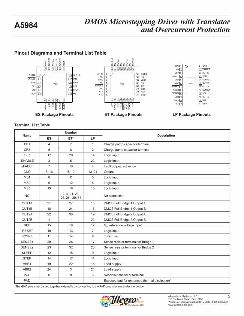
NameNumber
DescriptionES ET* LP
CP1 4 7 1 Charge pump capacitor terminal
CP2 5 8 2 Charge pump capacitor terminal
DIR 17 20 14 Logic input
E N A B L E 2 5 23 Logic input
nFAULT 7 10 4 Fault output, active low
GND 3, 16 6, 19 13, 24 Ground
MS1 8 11 5 Logic input
MS2 9 12 6 Logic input
MS3 13 16 10 Logic input
NC – 2, 4, 21, 23, 26, 28, 29, 31 – No connection
OUT1A 21 27 18 DMOS Full Bridge 1 Output A
OUT1B 18 24 15 DMOS Full Bridge 1 Output B
OUT2A 22 30 19 DMOS Full Bridge 2 Output A
OUT2B 1 1 22 DMOS Full Bridge 2 Output B
REF 15 18 12 Gm reference voltage input
R E S E T 10 13 7 Logic input
ROSC 11 14 8 Timing set
SENSE1 20 25 17 Sense resistor terminal for Bridge 1
SENSE2 23 32 20 Sense resistor terminal for Bridge 2
S L E E P 12 15 9 Logic input
STEP 14 17 11 Logic input
VBB1 19 22 16 Load supply
VBB2 24 3 21 Load supply
VCP 6 9 3 Reservoir capacitor terminal
PAD – – – Exposed pad for enhanced thermal dissipation*
*The GND pins must be tied together externally by connecting to the PAD ground plane under the device.
Pinout Diagrams and Terminal List Table
ES Package Pinouts ET Package Pinouts LP Package Pinouts
PAD
12345678
2423222120191817
9 10 11 12 13 14 15 16
32 31 30 29 28 27 26 25
SE
NS
E2
NC
OU
T2A
NC
NC
OU
T1A
NC
SE
NS
E1
VC
PnF
AU
LTM
S1
MS
2R
ES
ET
RO
SC
SLE
EP
MS
3
OUT1BNCVBB1NCDIRGNDREFSTEP
OUT2BNC
VBB2NC
ENABLEGNDCP1CP2
PAD
18
17
16
15
14
13
1
2
3
4
5
6
7 8 9 10 11 12
24 23 22 21 20 19
VB
B2
SE
NS
E2
OU
T2A
OU
T1A
SE
NS
E1
VB
B1
nFA
ULT
MS
1
MS
2
RE
SE
T
RO
SC
SLE
EP
OUT1B
DIR
GND
REF
STEP
MS3
OUT2B
ENABLE
GND
CP1
CP2
VCP
1
2
3
4
5
6
7
8
9
10
11
12
24
23
22
21
20
19
18
17
16
15
14
13
GND
ENABLE
OUT2B
VBB2
SENSE2
OUT2A
OUT1A
SENSE1
VBB1
OUT1B
DIR
GND
CP1
CP2
VCP
nFAULT
MS1
MS2
RESET
ROSC
SLEEP
MS3
STEP
REF
PAD
Terminal List Table

DMOS Microstepping Driver with Translatorand Overcurrent ProtectionA5984
6Allegro MicroSystems, LLC115 Northeast Cutoff, Box 15036Worcester, Massachusetts 01615-0036 (508) 853-5000www.allegromicro.com
ELECTRICAL CHARACTERISTICS [1] valid at TA = 25°C, VBB = 40 V (unless otherwise noted)Characteristics Symbol Test Conditions Min. Typ. [2] Max. Units
OUTPUT DRIVERS
Load Supply Voltage Range VBBOperating 8 – 40 V
During Sleep Mode 0 – 40 V
Output On Resistance RDS(on)Source + Sink Driver, IOUT = –2 A, TA = 25°C – 640 860 mΩ
Body Diode Forward Voltage VFSource Diode, IF = –2 A – – 1.4 V
Sink Diode, IF = 2 A – – 1.4 V
Output Driver Slew Rate SROUT 10% to 90% 50 100 150 ns
Motor Supply Current IBB
fPWM < 50 kHz – 7.5 10 mA
Operating, outputs disabled – 6.5 8 mA
Sleep Mode – – 10 μA
CONTROL LOGIC
Logic Input Voltage
VIN(1) 2 – – V
VIN(0) – – 0.8 V
VIN(SLEEP) – – 0.4 V
Logic Input CurrentIIN(1) –20 <1.0 20 µA
IIN(0) –20 <1.0 20 µA
Microstep Select Pins Internal Pull-Down Resistance RMSx MS1, MS2, or MS3 pin – 100 – kΩ
Logic Input Hysteresis VHYS(IN) 200 – 550 mV
Blank Time tBLANK 0.7 1 1.3 μs
Fixed Off-Time tOFF
ROSC = 5 V 20 30 40 μs
ROSC = GND 13 16 19 μs
ROSC = 25 kΩ 23 30 37 μs
Reference Input Voltage Range VREF 0 – 4 V
Reference Input Current IREF –3 0 3 μA
Current Trip-Level Error [3] errI
VREF = 2 V, %ITripMAX = 38.27% – – ±15 %
VREF = 2 V, %ITripMAX = 70.71% – – ±5 %
VREF = 2 V, %ITripMAX = 100.00% – – ±5 %
Crossover Dead Time tDT 100 475 800 ns
Fault Output Voltage VRST nFAULT pin, IOUT = 1 mA – – 0.5 V
Fault Output Leakage Current ILK nFAULT pin, no fault, pull-up to 5 V – – 1 µA
PROTECTIONOvercurrent Protection Threshold [4] IOCPST 2.6 – – A
VBB UVLO VBBUVLO VBB rising 6.3 – 6.85 V
VBB UVLO Hysteresis VBBHYS – 300 – mV
Thermal Shutdown Temperature TTSD – 165 – °C
Thermal Shutdown Hysteresis TTSDHYS – 20 – °C
1 For input and output current specifications, negative current is defined as coming out of (sourcing) the specified device pin.2 Typical data are for initial design estimations only, and assume optimum manufacturing and application conditions. Performance may vary for individual units, within the
specified maximum and minimum limits.3 VERR = [(VREF/8) – VSENSE] / (VREF/8).4 Overcurrent protection (OCP) is tested at TA = 25°C in a restricted range and guaranteed by characterization.

DMOS Microstepping Driver with Translatorand Overcurrent ProtectionA5984
7Allegro MicroSystems, LLC115 Northeast Cutoff, Box 15036Worcester, Massachusetts 01615-0036 (508) 853-5000www.allegromicro.com
THERMAL CHARACTERISTICS may require derating at maximum conditionsCharacteristic Symbol Test Conditions* Value Units
Package Thermal Resistance RθJA
ES package; estimated, on 4-layer PCB, based on JEDEC standard 37 °C/W
ET package; estimated, on 4-layer PCB, based on JEDEC standard 32 °C/W
LP package; on 4-layer PCB, based on JEDEC standard 28 °C/W
*In still air. Additional thermal information available on Allegro website.
20 40 60 80 100 120 140 160 180Temperature (°C)
Pow
er D
issi
patio
n, P
D (W
)
0.0
0.5
2.0
2.5
3.0
3.5
4.0
4.5
5.0
5.5
1.0
1.5
Maximum Power Dissipation, PD(max)
RθJA = 37 ºC/W
RθJA = 28 ºC/W
RθJA = 32 ºC/W
DMOS Microstepping Driver with Translatorand Overcurrent ProtectionA5984
8Allegro MicroSystems, LLC115 Northeast Cutoff, Box 15036Worcester, Massachusetts 01615-0036 (508) 853-5000www.allegromicro.com
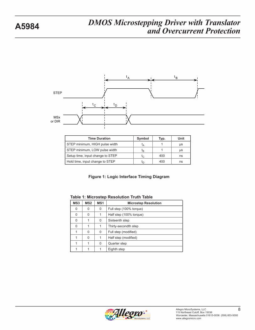
Figure 1: Logic Interface Timing Diagram
STEP
t A
t D t C
MSx RESET, or DIR
t B
Time Duration Symbol Typ. UnitSTEP minimum, HIGH pulse width tA 1 μs
STEP minimum, LOW pulse width tB 1 μs
Setup time, input change to STEP tC 400 ns
Hold time, input change to STEP tD 400 ns
Table 1: Microstep Resolution Truth TableMS3 MS2 MS1 Microstep Resolution
0 0 0 Full step (100% torque)
0 0 1 Half step (100% torque)
0 1 0 Sixteenth step
0 1 1 Thirty-secondth step
1 0 0 Full step (modified)
1 0 1 Half step (modified)
1 1 0 Quarter step
1 1 1 Eighth step
DMOS Microstepping Driver with Translatorand Overcurrent ProtectionA5984
9Allegro MicroSystems, LLC115 Northeast Cutoff, Box 15036Worcester, Massachusetts 01615-0036 (508) 853-5000www.allegromicro.com
The other method of current control utilizes slow decay mode when current is rising and mixed decay mode (31.25%) when current is falling. This method is exactly the same as A4984 series of stepper motor drivers. This method may be desired for drop-in applications to A4984 series. The current waveform and motor performance should be identical to A4984. The mixed decay waveforms for this method are shown in Figure 2. This form of current control is selected by connecting pin ROSC to greater than 3 V or by connecting a resistor from ROSC to GND. The Resistor option is used to adjust the off-time as desired (see ROSC section).
100 Percent Torque OperationIn full- and half-step modes, the device can be programmed so both phases are at ±100% current levels for full step mode, and either ±100% or 0% for half step mode.
Microstep Select (MSx)The microstep resolution is set by the voltage on logic inputs MSx, as shown in Table 1. Each MSx pin has an internal 100 kΩ pull-down resistance. When changing the step mode the change does not take effect until the next STEP rising edge.
If the step mode is changed without a translator reset, and abso-lute position must be maintained, it is important to change the step mode at a step position that is common to both step modes in order to avoid missing steps. When the device is powered down, or reset due to TSD or an over current event the translator is set to the home position which is by default common to all step modes.
Reset Input (RESET)The R E S E T input sets the translator to a predefined Home state (shown in Phase Current Diagrams section), and turns off all of the FET outputs. All STEP inputs are ignored until the R E S E T input is set to high.
FUNCTIONAL DESCRIPTION
Device OperationThe A5984 is a complete microstepping motor driver with a built-in translator for easy operation with minimal control lines. It is designed to operate bipolar stepper motors in full, half, quar-ter, eighth, sixteenth, or thirty-secondth step modes. The currents in each of the two output full-bridges and all of the N-channel DMOS FETs are regulated with fixed off-time PWM (pulse width modulated) control circuitry. At each step, the current for each full-bridge is set by the value of its external current-sense resistor (RS1 and RS2), a reference voltage (VREF), and the output voltage of its DAC (which in turn is controlled by the output of the translator).
At power-on or reset, the translator sets the DACs and the phase current polarity to the initial Home state (shown in the Phase Current Diagrams section), and the current regulator to Mixed Decay Mode for both phases. When a step command signal occurs on the STEP input, the translator automatically sequences the DACs to the next level and current polarity. (See Table 2 for the current-level sequence.) The microstep resolution is set by the combined effect of the MSx inputs, as shown in Table 1.
Stepping Current Control The A5984 has two methods of current control. The first method of current control is called Adaptive Percent Fast Decay (APFD). APFD is selected by connecting pin ROSC to GND. Essentially, the IC determines the proper amount of fast decay on both rising and falling currents. By only adding fast decay when needed, the output current more accurately tracks the input command from the D-to-A converter and solves the basic problem of current discontinuity through zero when stepping at slow speeds (see Figure 4). This will result in a performance advantage for slow-speed high-resolution stepping such as with security camera applications. An additional benefit of APFD is reduced current ripple across the various operating conditions and motor characteristics.

DMOS Microstepping Driver with Translatorand Overcurrent ProtectionA5984
10Allegro MicroSystems, LLC115 Northeast Cutoff, Box 15036Worcester, Massachusetts 01615-0036 (508) 853-5000www.allegromicro.com
VSTEP
IOUT
IOUT
t
See Enlargement A
Enlargement A
tSDtFD
toff
Slow Decay
Mixed Decay
Fast Decay
IPEAK
70.71
–70.71
0
100.00
–100.00
Symbol Characteristictoff Device fixed off-time
IPEAK Maximum output current
tSD Slow decay interval
tFD Fast decay interval
IOUT Device output current
Figure 2: Current Decay Modes Timing Chart

DMOS Microstepping Driver with Translatorand Overcurrent ProtectionA5984
11Allegro MicroSystems, LLC115 Northeast Cutoff, Box 15036Worcester, Massachusetts 01615-0036 (508) 853-5000www.allegromicro.com
Figure 3: Missed Steps in Low-Speed Microstepping
Figure 4: Continuous Stepping Using APFD (ROSC Pin Grounded)
t → , 1 s/div.Step input 10 V/div.
Mixed Decay
No Missed StepsILOAD 500 mA/div.
t → , 1 s/div.Step input 10 V/div.
Slow Decay
Slow Decay
Slow Decay
Slow Decay
MixedDecay
MixedDecay
MixedDecay
MixedDecay
Missed Step

DMOS Microstepping Driver with Translatorand Overcurrent ProtectionA5984
12Allegro MicroSystems, LLC115 Northeast Cutoff, Box 15036Worcester, Massachusetts 01615-0036 (508) 853-5000www.allegromicro.com
Step Input (STEP)A low-to-high transition on the STEP input sequences the transla-tor and advances the motor one increment. The translator controls the input to the DACs and the direction of current flow in each winding. The size of the increment is determined by the combined state of the MSx inputs.
Direction Input (DIR)This determines the direction of rotation of the motor. Setting to logic high and logic low set opposite rotational directions. Changes to this input do not take effect until the next STEP input rising edge. Refer to Phase Current diagrams (Figures 10 to 17). For DIR = LOW, currents change sequentially clockwise around the circle. For DIR = HIGH, counterclockwise.
Internal PWM Current ControlEach full-bridge is controlled by a fixed off-time PWM current control circuit that limits the load current to a desired value, ITRIP . Initially, a diagonal pair of source and sink FET outputs are enabled and current flows through the motor winding and the current sense resistor, RSx. When the voltage across RSx equals the DAC output voltage, the current sense comparator resets the PWM latch. The latch then turns off either the source FET (when in Slow decay mode) or the sink and source FETs (when in Mixed decay mode).
The maximum value of current limiting is set by the selection of RSx and the voltage at the VREF pin. The transconductance func-tion is approximated by the maximum value of current limiting, ITripMAX (A), which is set by
ITripMAX = VREF / ( 8 × RS)where RS is the resistance of the sense resistor (Ω) and VREF is the input voltage on the REF pin (V).
The DAC output reduces the VREF output to the current sense comparator in precise steps, such that
Itrip = (%ITripMAX / 100) × ITripMAX
(See table 2 for %ITripMAX at each step.)
It is critical that the maximum rating (0.5 V) on the SENSE1 and SENSE2 pins is not exceeded.
BlankingThis function blanks the output of the current sense comparators when the outputs are switched by the internal current control circuitry. The comparator outputs are blanked to prevent false overcurrent detection due to reverse recovery currents of the clamp diodes, and switching transients related to the capacitance of the load. The blank time, tBLANK (µs), is approximately
tBLANK ≈ 1 µs
ROSCThe configuration of the ROSC terminal determines both the method of current control as well as the fixed off-time (tOFF).
ROSC Decay Mode tOFF
GNDAPFD
(Adaptive Percent Fast Decay Mode)
16 µs
Resistor to GND
Slow Decay Rising Current StepsMixed Decay Falling Current Steps ROSC/825 (µs)
Pulled Up to > 3 V Supply
Slow Decay Rising Current StepsMixed Decay Falling Current Steps 30 µs
Charge Pump (CP1 and CP2)The charge pump is used to generate a gate supply greater than that of VBB for driving the source-side FET gates. A 0.1 µF ceramic capacitor, should be connected between CP1 and CP2. In addition, a 0.1 µF ceramic capacitor is required between VCP and VBB, to act as a reservoir for operating the high-side FET gates.
Capacitor values should be Class 2 dielectric ±15% maximum, or tolerance R, according to EIA (Electronic Industries Alliance) specifications.
Enable Input (ENABLE)This input turns on or off all of the FET outputs. When set to a logic high, the outputs are disabled. When set to a logic low, the internal control enables the outputs as required. The translator inputs STEP, DIR, and MSx, as well as the internal sequencing logic, all remain active, independent of the E N A B L E input state.
Sleep Mode (SLEEP)To minimize power consumption when the motor is not in use, SLEEP disables much of the internal circuitry including the

DMOS Microstepping Driver with Translatorand Overcurrent ProtectionA5984
13Allegro MicroSystems, LLC115 Northeast Cutoff, Box 15036Worcester, Massachusetts 01615-0036 (508) 853-5000www.allegromicro.com
output FETs, current regulator, and charge pump. A logic low on the S L E E P pin puts the A5984 into Sleep mode. A logic high allows normal operation, as well as start-up (at which time the A5984 drives the motor to the Home microstep position). When emerging from Sleep mode, in order to allow the charge pump to stabilize, provide a delay of 1 ms before issuing a Step command.
Synchronous RectificationWhen a PWM-off cycle is triggered by an internal fixed-off time cycle, load current recirculates according to the decay mode selected by the control logic. This synchronous rectification feature turns on the appropriate FETs during current decay, and effectively shorts out the body diodes with the low FET RDS(on). This reduces power dissipation significantly, and can eliminate the need for external Schottky diodes in many applications. Syn-chronous rectification turns off when the load current approaches zero (0 A), preventing reversal of the load current.
Protection FunctionsFAULT OUTPUT (nFAULT)An open drain fault output is provided to notify the user if the IC has been disabled due to an OCP event. If an OCP event is trig-gered the device will be disabled and the outputs will be latched off. The active low nFAULT output will be enabled. The latch can be reset by commanding S L E E P or R E S E T low, or by bringing VBB below its UVLO threshold.
THERMAL OR UNDERVOLTAGE FAULT SHUTDOWNIn the event of a fault, overtemperature (excess TJ) or an under-voltage (on VCP), the FET outputs of the A5984 are disabled until the fault condition is removed. At power-on, the UVLO (undervoltage lockout) circuit disables the FET outputs and resets the translator to the Home state.
OVERCURRENT PROTECTIONA current monitor will protect the IC from damage due to output shorts. If a short is detected, the IC will latch the fault and disable the outputs. The fault latch can only be cleared by coming out of Sleep mode or by cycling the power to VBB. During OCP events, Absolute Maximum Ratings may be exceeded for a short period of time before the device latches (see Figure 5).
Figure 5: Overcurrent Event
t →
5 A / div.Fault latched

DMOS Microstepping Driver with Translatorand Overcurrent ProtectionA5984
14Allegro MicroSystems, LLC115 Northeast Cutoff, Box 15036Worcester, Massachusetts 01615-0036 (508) 853-5000www.allegromicro.com
APPLICATION INFORMATION
LayoutThe printed circuit board should use a heavy groundplane. For optimum electrical and thermal performance, the A5984 must be soldered directly onto the board. On the underside of the A5984 package is an exposed pad, which provides a path for enhanced thermal dissipation. The thermal pad should be soldered directly to an exposed surface on the PCB. Thermal vias are used to transfer heat to other layers of the PCB (see Figure 6).
In order to minimize the effects of ground bounce and offset issues, it is important to have a low-impedance single-point ground, known as a star ground, located very close to the device. By making the connection between the pad and the ground plane directly under the A5984, that area becomes an ideal location for a star ground point. A low-impedance ground will prevent ground bounce during high-current operation and ensure that the supply voltage remains stable at the input terminal.
The two input capacitors should be placed in parallel, and as close to the device supply pins as possible (see Figure 8). The ceramic capacitor (C7) should be closer to the pins than the bulk capacitor (C2). This is necessary because the ceramic capacitor will be responsible for delivering the high-frequency current components.
The sense resistors, RSx , should have a very low-impedance path to ground, because they must carry a large current while supporting very accurate voltage measurements by the current sense comparators. Long ground traces will cause additional voltage drops, adversely affecting the ability of the comparators to accurately measure the current in the windings. The SENSEx pins have very short traces to the RSx resistors and very thick, low-impedance traces directly to the star ground underneath the device. If possible, there should be no other components on the sense circuits.
PCB
Thermal Vias
Trace (2 oz.)Signal (1 oz.)Ground (1 oz.)Thermal (2 oz.)
SolderA5984
OUT2B
ENABLE
GND
CP1
CP2
VCP
nFFA
ULT
MS
1
MS
2
RE
SE
T
RO
SC
SLE
EP
OUT1B
DIR
GND
REF
STEP
MS3
VB
B2
SE
NS
E2
OU
T2A
OU
T1A
SE
NS
E1
VB
B1
VBB
C2ROSC
PAD
A5984
C7
C3
C4
R4 R5
OUT2B OUT1A OUT1BOUT2A
R4
U1
OUT2B
GND
R5
OUT2A OUT1A OUT1B
GND
GND
GND
C3
C4
ROSCC2
C7
VBB
CAPACITANCE
BULK
Figure 7: ES Package Circuit Layout Figure 8: ES Package Typical Application
Figure 6: Soldering Cross-Section

DMOS Microstepping Driver with Translatorand Overcurrent ProtectionA5984
15Allegro MicroSystems, LLC115 Northeast Cutoff, Box 15036Worcester, Massachusetts 01615-0036 (508) 853-5000www.allegromicro.com
VCP
GND
CP2
GND
CP1VBB
8 V
GND
GND GND
8 V
SENSE VINT
GND
VBB
48 V
GND
VBB
OUTDMOSParasitic
DMOSParasitic
SENSE
PGND GND
MSxDIR
VREFROSC
SLEEPRESET
ENABLESTEP
Pin Circuit Diagrams
Figure 9: Pin Circuit Diagrams
9a 9b
9c 9d 9e
DMOS Microstepping Driver with Translatorand Overcurrent ProtectionA5984
16Allegro MicroSystems, LLC115 Northeast Cutoff, Box 15036Worcester, Massachusetts 01615-0036 (508) 853-5000www.allegromicro.com
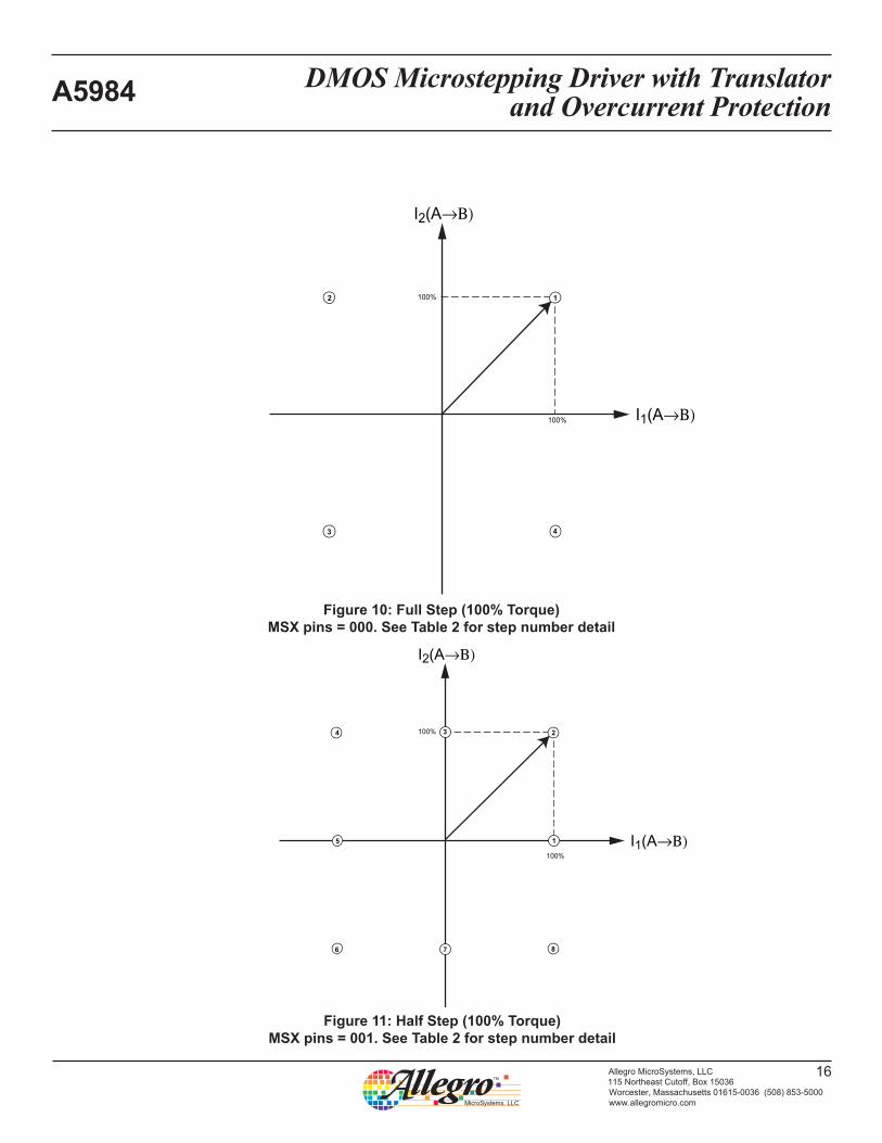
Figure 10: Full Step (100% Torque)MSX pins = 000. See Table 2 for step number detail
Figure 11: Half Step (100% Torque)MSX pins = 001. See Table 2 for step number detail
I1(A→Β)
I2(A→Β)
100%
100%
234
5
6 7 8
1
I1(A→Β)
I2(A→Β)
100%
100%
12
3 4

I1(A→Β)
I2(A→Β)
70%
70%
17
33
49
65
81
97
113
1
I1(A→Β)
I2(A→Β)
70%
70%
9
17
25
33
41
49
57
1
DMOS Microstepping Driver with Translatorand Overcurrent ProtectionA5984
17Allegro MicroSystems, LLC115 Northeast Cutoff, Box 15036Worcester, Massachusetts 01615-0036 (508) 853-5000www.allegromicro.com
Figure 12: Sixteenth StepMSX pins = 010. See Table 3 for step number detail
Figure 13: Thirty-Second StepMSX pins = 011. See Table 3 for step number detail

I1(A→Β)
I2(A→Β)
70%
70%
2
3
4
5
6
7
8
1
I1(A→Β)
I2(A→Β)
70%
70%
12
3 4
DMOS Microstepping Driver with Translatorand Overcurrent ProtectionA5984
18Allegro MicroSystems, LLC115 Northeast Cutoff, Box 15036Worcester, Massachusetts 01615-0036 (508) 853-5000www.allegromicro.com
Figure 14: Full Step (70% Torque)MSX pins = 100. See Table 3 for step number detail
Figure 15: Half Step (70% Torque)MSX pins = 101. See Table 3 for step number detail
I1(A→Β)
I2(A→Β)
70%
70%
5
9
13
17
21
25
29
1
I1(A→B)
I2(A→B)
70%
70%
3
5
7
9
11
13
15
1
DMOS Microstepping Driver with Translatorand Overcurrent ProtectionA5984
19Allegro MicroSystems, LLC115 Northeast Cutoff, Box 15036Worcester, Massachusetts 01615-0036 (508) 853-5000www.allegromicro.com
Figure 16: Quarter StepMSX pins = 110. See Table 3 for step number detail
Figure 17: Eighth StepMSX pins = 111. See Table 3 for step number detail

DMOS Microstepping Driver with Translatorand Overcurrent ProtectionA5984
20Allegro MicroSystems, LLC115 Northeast Cutoff, Box 15036Worcester, Massachusetts 01615-0036 (508) 853-5000www.allegromicro.com
Table 2: Stepping Phase Table, Full Torque Modes
Full (100%) Half Step (100%) AngleWinding Current 1
(%)Winding Current 2
(%)1 0 100 0
1 2 45 100 100
3 90 0 100
2 4 135 –100 100
5 180 –100 0
3 6 225 –100 –100
7 270 0 –100
4 8 315 100 –100
Stepping Phase Tables
DMOS Microstepping Driver with Translatorand Overcurrent ProtectionA5984
21Allegro MicroSystems, LLC115 Northeast Cutoff, Box 15036Worcester, Massachusetts 01615-0036 (508) 853-5000www.allegromicro.com
Full (70%) Half (70%) 1/4 Step 1/8 Step 1/16 Step 1/32 Step Angle Winding Current 1 (%)
Winding Current 2 (%)
1 1 1 1 1 0 100 0
2 2.8 100 5
2 3 5.6 100 10
4 8.4 99 15
2 3 5 11.3 98 20
6 14.1 97 24
4 7 16.9 96 29
8 19.7 94 34
2 3 5 9 22.5 92 38
10 25.3 90 43
6 11 28.1 88 47
12 30.9 86 51
4 7 13 33.8 83 56
14 36.6 80 60
8 15 39.4 77 63
16 42.2 74 67
1 2 3 5 9 17 45 71 71
18 47.8 67 74
10 19 50.6 63 77
20 53.4 60 80
6 11 21 56.3 55 83
22 59.1 51 86
12 23 61.9 47 88
24 64.7 43 90
4 7 13 25 67.5 38 92
26 70.3 34 94
14 27 73.1 29 96
28 75.9 24 97
8 15 29 78.8 19 98
30 81.6 15 99
16 31 84.4 10 100
32 87.2 5 100
3 5 9 17 33 90 0 100
Table 3: Stepping Phase Table, Common Modes
Continued on the next page…

DMOS Microstepping Driver with Translatorand Overcurrent ProtectionA5984
22Allegro MicroSystems, LLC115 Northeast Cutoff, Box 15036Worcester, Massachusetts 01615-0036 (508) 853-5000www.allegromicro.com
Full (70%) Half (70%) 1/4 Step 1/8 Step 1/16 Step 1/32 Step Angle Winding Current 1 (%)
Winding Current 2 (%)
34 92.8 –5 100
18 35 95.6 –10 100
36 98.4 –15 99
10 19 37 101.3 –20 98
38 104.1 –24 97
20 39 106.9 –29 96
40 109.7 –34 94
6 11 21 41 112.5 –38 92
42 115.3 –43 90
22 43 118.1 –47 88
44 120.9 –51 86
12 23 45 123.8 –56 83
46 126.6 –60 80
24 47 129.4 –63 77
48 132.2 –67 74
2 4 7 13 25 49 135 –71 71
50 137.8 –74 67
26 51 140.6 –77 63
52 143.4 –80 60
14 27 53 146.3 –83 55
54 149.1 –86 51
28 55 151.9 –88 47
56 154.7 –90 43
8 15 29 57 157.5 –92 38
58 160.3 –94 34
30 59 163.1 –96 29
60 165.9 –97 24
16 31 61 168.8 –98 19
62 171.6 –99 15
32 63 174.4 –100 10
64 177.2 –100 5
5 9 17 33 65 180 –100 0
66 182.8 –100 –5
Stepping Phase Table, Common Modes (continued)
Continued on the next page…

DMOS Microstepping Driver with Translatorand Overcurrent ProtectionA5984
23Allegro MicroSystems, LLC115 Northeast Cutoff, Box 15036Worcester, Massachusetts 01615-0036 (508) 853-5000www.allegromicro.com
Full (70%) Half (70%) 1/4 Step 1/8 Step 1/16 Step 1/32 Step Angle Winding Current 1 (%)
Winding Current 2 (%)
34 67 185.6 –100 –10
68 188.4 –99 –15
18 35 69 191.3 –98 –20
70 194.1 –97 –24
36 71 196.9 –96 –29
72 199.7 –94 –34
10 19 37 73 202.5 –92 –38
74 205.3 –90 –43
38 75 208.1 –88 –47
76 210.9 –86 –51
20 39 77 213.8 –83 –56
78 216.6 –80 –60
40 79 219.4 –77 –63
80 222.2 –74 –67
3 6 11 21 41 81 225 –71 –71
82 227.8 –67 –74
42 83 230.6 –63 –77
84 233.4 –60 –80
22 43 85 236.3 –55 –83
86 239.1 –51 –86
44 87 241.9 –47 –88
88 244.7 –43 –90
12 23 45 89 247.5 –38 –92
90 250.3 –34 –94
46 91 253.1 –29 –96
92 255.9 –24 –97
24 47 93 258.8 –19 –98
94 261.6 –15 –99
48 95 264.4 –10 –100
96 267.2 –5 –100
7 13 25 49 97 270 0 –100
98 272.8 5 –100
Stepping Phase Table, Common Modes (continued)
Continued on the next page…

DMOS Microstepping Driver with Translatorand Overcurrent ProtectionA5984
24Allegro MicroSystems, LLC115 Northeast Cutoff, Box 15036Worcester, Massachusetts 01615-0036 (508) 853-5000www.allegromicro.com
Full (70%) Half (70%) 1/4 Step 1/8 Step 1/16 Step 1/32 Step Angle Winding Current 1 (%)
Winding Current 2 (%)
50 99 275.6 10 –100
100 278.4 15 –99
26 51 101 281.3 20 –98
102 284.1 24 –97
52 103 286.9 29 –96
104 289.7 34 –94
14 27 53 105 292.5 38 –92
106 295.3 43 –90
54 107 298.1 47 –88
108 300.9 51 –86
28 55 109 303.8 56 –83
110 306.6 60 –80
56 111 309.4 63 –77
112 312.2 67 –74
4 8 15 29 57 113 315 71 –71
114 317.8 74 –67
58 115 320.6 77 –63
116 323.4 80 –60
30 59 117 326.3 83 –55
118 329.1 86 –51
60 119 331.9 88 –47
120 334.7 90 –43
16 31 61 121 337.5 92 –38
122 340.3 94 –34
62 123 343.1 96 –29
124 345.9 97 –24
32 63 125 348.8 98 –19
126 351.6 99 –15
64 127 354.4 100 –10
128 357.2 100 –5
Stepping Phase Table, Common Modes (continued)

DMOS Microstepping Driver with Translatorand Overcurrent ProtectionA5984
25Allegro MicroSystems, LLC115 Northeast Cutoff, Box 15036Worcester, Massachusetts 01615-0036 (508) 853-5000www.allegromicro.com
For Reference Only – Not for Tooling Use(Reference JEDEC MO-220WGGD)
Dimensions in millimeters – NOT TO SCALEExact case and lead configuration at supplier discretion within limits shown
C
SEATINGPLANE
C0.08
21X
2
1
1
2
2
1A
A
B
C
D
D
C
4.00 ±0.15
4.00 ±0.15 4.10
0.30 0.50
4.100.75 ±0.05
0.40 MAX
0.25+0.05–0.07
B
PCB Layout Reference View
Terminal #1 mark area
Exposed thermal pad (reference only, terminal #1 identifier appearance at supplier discretion)
Reference land pattern layout (reference IPC7351 QFN50P400X400X80-25W6M);all pads a minimum of 0.20 mm from all adjacent pads; adjust as necessary to meetapplication process requirements and PCB layout tolerances; when mounting on amultilayer PCB, thermal vias at the exposed thermal pad land can improve thermaldissipation (reference EIA/JEDEC Standard JESD51-5)
Coplanarity includes exposed thermal pad and terminals
0.95
24
24
24
2.70
2.70
2.70
2.70
0.50
Figure 18: ES Package, 24-Pin QFN with Exposed Thermal Pad
PACKAGE OUTLINE DRAWINGS
DMOS Microstepping Driver with Translatorand Overcurrent ProtectionA5984
26Allegro MicroSystems, LLC115 Northeast Cutoff, Box 15036Worcester, Massachusetts 01615-0036 (508) 853-5000www.allegromicro.com
Figure 19: ET Package, 32-Pin QFN with Exposed Thermal Pad
For Reference Only – Not for Tooling Use(Reference JEDEC MO-220VHHD-5)
Dimensions in millimeters – NOT TO SCALEExact case and lead configuration at supplier discretion within limits shown
32
32
2
1
2
1
A
A
B
C
B
32
2
1
3.40
3.40
0.50 BSC
5.00 ±0.05
5.00 ±0.05
0.90 ±0.10
0.25+0.05-0.07
0.40 ±0.10
3.40
3.40
0.30
1
0.50
1.00
5.00
5.00
C
C0.08
33X
SEATINGPLANE
CD
D
PCB Layout Reference View
Terminal #1 mark area
Exposed thermal pad (reference only, terminal #1 identifier appearance at supplierdiscretion)
Reference land pattern layout (reference IPC7351 QFN50P500X500X100-33V6M);all pads a minimum of 0.20 mm from all adjacent pads; adjust as necessary to meetapplication process requirements and PCB layout tolerances; when mounting on amultilayer PCB, thermal vias at the exposed thermal pad land can improve thermaldissipation (reference EIA/JEDEC Standard JESD51-5)
Coplanarity includes exposed thermal pad and terminals

DMOS Microstepping Driver with Translatorand Overcurrent ProtectionA5984
27Allegro MicroSystems, LLC115 Northeast Cutoff, Box 15036Worcester, Massachusetts 01615-0036 (508) 853-5000www.allegromicro.com
Figure 20: LP Package, 24-Pin TSSOP with Exposed Thermal Pad
For Reference Only – Not for Tooling Use(Reference MO-153 ADT)
NOT TO SCALEDimensions in millimeters
Dimensions exclusive of mold flash, gate burrs, and dambar protrusionsExact case and lead configuration at supplier discretion within limits shown
A
1.20 MAX
0.150.00
0.300.19
0.200.09
8º0º
0.60 ±0.15 1.00 REF
C
SEATINGPLANE
C0.10
24X
0.65 BSC
0.25 BSC
21
24
7.80 ±0.10
4.40±0.10 6.40±0.20
GAUGE PLANE
SEATING PLANE
A
B
B
Exposed thermal pad (bottom surface); dimensions may vary with device
4.32 NOM
3 NOM
0.65
6.103.00
4.32
1.65
0.45
C
C
PCB Layout Reference View
Terminal #1 mark area
Reference land pattern layout (reference IPC7351 TSOP65P640X120-25M);all pads a minimum of 0.20 mm from all adjacent pads; adjust as necessaryto meet application process requirements and PCB layout tolerances; whenmounting on a multilayer PCB, thermal vias at the exposed thermal pad landcan improve thermal dissipation (reference EIA/JEDEC Standard JESD51-5)

DMOS Microstepping Driver with Translatorand Overcurrent ProtectionA5984
28Allegro MicroSystems, LLC115 Northeast Cutoff, Box 15036Worcester, Massachusetts 01615-0036 (508) 853-5000www.allegromicro.com
For the latest version of this document, visit our website:
www.allegromicro.com
REVISION HISTORYNumber Date Description
– January 19, 2016 Initial release
1 April 26, 2016 Updated Pin Circuit Diagrams 9c and 9e on page 15
2 January 3, 2017 Added VBB UVLO and VBB UVLO Hysteresis characteristics to page 6
Copyright ©2017, Allegro MicroSystems, LLCAllegro MicroSystems, LLC reserves the right to make, from time to time, such departures from the detail specifications as may be required to
permit improvements in the performance, reliability, or manufacturability of its products. Before placing an order, the user is cautioned to verify that the information being relied upon is current.
Allegro’s products are not to be used in any devices or systems, including but not limited to life support devices or systems, in which a failure of Allegro’s product can reasonably be expected to cause bodily harm.
The information included herein is believed to be accurate and reliable. However, Allegro MicroSystems, LLC assumes no responsibility for its use; nor for any infringement of patents or other rights of third parties which may result from its use.