a0-diode pumped chassis - fermilabeddata.fnal.gov/lasso/summerstudents/papers/2011/clarke.pdfthis...
TRANSCRIPT

A0-Diode Pumped Chassis
Courtney Clarke
School of Engineering and Applied Science Miami University
Oxford, OH 45056
Jinhao Ruan and James Santucci A0PI
Accelerator Division Fermilab National Accelerator Laboratory
Batavia, IL 60510
Summer Internship in Science and Technology (SIST) Program Date: August 11, 2011
Abstract This report documents the production of the first Diode pumped chassis for use in A0 laser laboratory. It will recount the tests conducted, the results, and the issues to be considered when producing the next system for future use.

Fermilab SIST 2011
2
Contents Abstract ......................................................................................................................................................... 1
Introduction ................................................................................................................................................... 3
Design ........................................................................................................................................................... 4
Parts & Important Components ................................................................................................................ 4
Top view. .............................................................................................................................................. 4
Front view. ............................................................................................................................................ 8
Back view. ............................................................................................................................................. 9
Considerations............................................................................................................................................... 9
Mounting the Diodes ................................................................................................................................. 9
Heat Dissipated by the Diode Driver ........................................................................................................ 9
Capacitors ............................................................................................... Error! Bookmark not defined.
Tests & Results ........................................................................................................................................... 10
Conclusion & Future Work ......................................................................................................................... 14
References ................................................................................................... Error! Bookmark not defined.
Appendix ..................................................................................................................................................... 15
A) Circuit Diagram .......................................................................................................................... 15
B) Matlab power_supply_control GUI for Analog control of the Bulk Supply .............................. 16
Interface .............................................................................................................................................. 16

Fermilab SIST 2011
3
Introduction
This report documents the installation and setup of the Diode Pumped Chassis that will replace the current diode source inside A0 laser laboratory. The configuration in A0 laser lab currently uses two diode drivers and two power supplies, however one diode driver should be sufficient to power up to 15 diodes. The diode pumped chassis will be used as the pump laser for two-pass and multi-pass diode pumped amplifiers. The configuration is shown in Figure [1].
Figure [2]: Animation of current diode pump for multi-pass amplifier. The multi-pass amplifier is used to amplify the seed lasers pulses to tens of μJ, and the two-pass will further amplify the signal to hundreds of μJ as it is directed towards the CsTe photocathode.
The primary difference between the current and new system is the use of one diode driver to power two separate diodes in series. In addition, new parts were also introduced into the system including:
- 2 X 800μm, 100 W, QCW Conduction cooled single bar fiber coupled modules - 1 X High Power CW or Pulsed Laser diode driver - 1 X DLM-600W Series M51A Option Isolated Analog Power supply
The expected performance specs of the system are an output of 100 W, a pulse width of 1 ms, and a 5 Hz repetition rate. The parts are installed into a chassis which can be mounted on any standard rack unit.

Fermilab SIST 2011
4
Design
Parts & Important Components
Top view.
Figure [3]: Top view.
1. Diodes
Two 800 μm, 100W, DCW Conduction Cooled Single Bar Fiber coupled Modules mounted beside an aluminum heat sink. These diodes are paired in series and electrically isolated from the heat sink, to disallow the chance of completely bypassing one or the other diode through the heat sink to chassis ground.
2. AC Power Supply 3. Diode driver
High power CW or Pulsed Laser Diode Driver that outputs 20 Amps CW or 120 Amps pulsed, and provides a pulse width to 1.0 ms1.
1 http://www.analogmodules.com/admincenter/datasheets/779a.pdf

Fermilab SIST 2011
5
Figure [4]: High power CW or Pulsed Laser Diode Driver 2
4. LED 5. Relay Switch 6. 120V to 24V Transformer 7. Terminal Block 8. Signals 9. AC in 10. Bulk DC power supply
DLM-600W Series M51A Option Isolated Analog Power supply, which provides a remote programmable option through its DB25 connector with the following setup.
Sorenson DLM 600W Bulk Supply Back Panel INTFC Switches
Figure [5]3: Back panel The DLM 600W power supply can be set to many different settings via the INTFC switches located on the back panel of DLM600W unit. Each of the 8 switches corresponds to a different function. The primary modes being utilized in A0 include: 0-10 V mode, low-logic external off control of the outputs, voltage and current monitor. This is achieved by the positioning of the switches. Even though the primary controls are the 0-10 V (position 1), voltage monitoring (position 4), and on/off control (position 6), the complete list of functions is below:
2 http://www.mjlinc.com/data/file/productimgs/1299305075552189922212.jpg 3 Back Panel. Figure 2-1 p. 2-3, Sorensen DLM 600W Series Power Supplies: M51A Option Isolated Analog

Fermilab SIST 2011
6
Table [1]4: INTFC Switches Switch Position Function OFF (Down) Position ON (Up) Position 1 V, 10V or 4-20mA Select 0-5VDC 0-10VDC or 4-20mA5 2 I, 10V or 4-20mA Select 0-5VDC 0-10VDC or 4-20mA 3 OVP, 10V Select 0-5VDC 0-10VDC 4 VMON, 10V Select 0-5VDC or 4-20mA 0-10VDC6 5 IMON, 10V Select 0-5VDC or 4-20mA 0-10VDC 6 EXT-OFF, Active-Low
Select Active-High Logic Level
Active-Low Logic Level7
7 LCK-OUT Enable Front Panel Controls
Lockout Front Panel
8 Not Used — —
4 Table 2-1 p.2-1, Sorensen DLM 600W Series Power Supplies: M51A Option Isolated Analog Programming Manual 5 Setting used in A0 Laser lab 6 Setting used in A0 Laser lab 7 Setting used in A0 Laser lab

Fermilab SIST 2011
7
DB25 Pin Configuration
Another feature that offers more control of the DLM600W bulk supply is the remote control option, which will allow for the manipulation of the diodes without the use of the front panel. This is achieved through the isolated analog interface that is programmed through a DB25 sub with the following pins configurations:
Table [2]8: Pin designations Pin Function
1 ANALOG-CONTROL input 2 Return for 0-5/10V monitor outputs and EXTERNAL-OFF 3 OVP programming input 4 Voltage monitor output, 4-20mA 5 VOLTAGE-MODE status output 6 Return for 4-20mA monitor outputs, Auxiliary 5VDC, and digital I/O 7 Current monitor output, 0-5/10V 8 1.25VDC output for 4-20mA voltage programming signal 9 Voltage programming input 10 Current programming input 11 1.25VDC output for 4-20mA current programming signal 12 Return for 0-5/10V or resistance programming signals 13 Return for 4-20mA current programming signal 14 EXTERNAL-OFF input 15 Auxiliary 5VDC output (+) 16 OVP resistance programming output, 1mA source 17 OVP status output 18 FAULT status output 19 Voltage monitor output, 0-5/10V 20 1.25V input for 4-20mA voltage programming signal 21 Voltage resistance programming output, 1mA source 22 Current resistance programming output, 1mA source 23 1.25V input for 4-20mA current programming signal 24 Current monitor output, 4-20mA 25 Return for 4-20mA voltage programming
Figure [6]9: DB25 connector
8 Table 2-2 p. 2-4, Sorensen DLM 600W Series Power Supplies: M51A Option Isolated Analog Programming Manual 9 Figure 4-2, p. 4-3, Sorensen DLM 600W Series Power Supplies: Operation Manual

Fermilab SIST 2011
8
Pin map for Voltage control (0-10V) to DB25 Each pin on the DB25 Isolated Analog Interface has a designation, for its current usage. Pins #15, #2, and #12 are the absolute reference pins tied to positive or ground, as shown in Table [3].
Table [4]: Positive & Ground Pins Positive pin #15 Negative pin (GND) #2, #12
The other pins are used to control the features enabled by the system when in remote control mode. These features are also available in manual mode via the front panel. The pin connections and designation are in Table [5].
Table [5]: Pin connections Control Positive pin Negative (return) Variable voltage (IRM) #9 #12 Voltage monitor #19 #2 Interlock #14 #2 Remote Operation Enable #1 -
Front view.
Figure [7]: Front panel view.
A. Power B. OVP preview in display C. LED indicators D. Local/Remote switch: keep in remote mode. E. Over voltage protection (OVP) preview F. EXT-OFF control G. Current control H. Voltage control I. Displays

Fermilab SIST 2011
9
Back view.
Figure [8]: Back panel view
A. Diode outputs B. Safety contacts input C. Current control D. Pulse Enable (High Z) E. Current monitor (High Z) F. Bulk voltage monitor (High Z) G. Chassis ground H. Bulk voltage control I. Fuse
It is important that designated parts of the back panel by configure with high impedance where denoted. A circuit diagram is available in the appendix.
Considerations
Mounting the Diodes When the diodes were first powered, light was only emitted from the second diode. The voltage across the two diodes revealed that the entire voltage was across the second diode, so the main reasons for this issue could be that the first diode was malfunctioning, or the diodes were not truly in series. Therefore the diodes were tested to guarantee that they were not broken. To test this, the diodes were switched in order to see if they behaved in the same manner. Since the problem remained only with the first diode in the series then the diodes were in fact functioning because the problem did not travel with the diode.
The resistance across the diodes was measured and since there was no resistance, then there was no current. The only one other component that connected the two diodes besides the copper connection was the heat sink. The aluminum heat sink provided a path of least resistance around the first diode to the second diode, so only after the heat sink was split into two separate pieces, and electrically isolated from chassis ground and the other diode did the diodes emit the same power.
Heat Dissipated by the Diode Driver Another important aspect to check is the amount of heat dissipated by the diode driver. Based on the desired usage, a forward bias of 2.5 V per diode, a maximum driving current of 120 A, the duty cycle of 1

Fermilab SIST 2011
10
ms over a time span of 200 ms then the amount of heat generated is 3 W. Based on the specification sheet provided by Analog Modules, Inc., they recommend a heat sink be installed for any amount greater than 20 W 10. Therefore a heat sink was not necessary for this application.
Tests & Results After setup, several tests were run on the unit to determine outputs in comparison to the specification sheets. The DLM600W was tested independently to verify the given properties. This unit was connected to a DC voltage via its programmable control option, the isolated analog interface DB25 connector. An important consideration for this test is that the remote operation mode is initiated when a voltage of between 3-15 VDC is connected to Pin 1 of the DB25 connector. Once this test was completed, the next step required the creation of a remote control program, which was completed in Matlab.
Figure [9]: Control GUI.
The program created in Matlab would communicate the desired voltage to the internet rack monitor (IRM11), which will send the appropriate voltage out to the DC bulk supply unit to power the laser diode driver to manage the current to the diodes. Therefore, it was necessary to define the voltage-current plot by use of the chassis voltage and current monitoring ports.
10 http://www.analogmodules.com/admincenter/datasheets/779a_an.pdf 11 http://www-inteng.fnal.gov/Integrated_Eng/irm/

Fermilab SIST 2011
11
Figure [10]: Current vs. Power plot The diode current vs. optical power was linearly fitted to the following equation:
( )
From here, the program could be used to set the diode current to a desired value. Furthermore, this program could perform fine adjustments on the voltage to reduce oscillations that appear as a result of poor coarse adjustments.
The output power of both diodes was also tested, and it was determined that the deviation between the diodes was minimal.
Figure [11]: Plot diode power results Unfortunately, because the diode driver used may not support a 1 ms pulse width with the plotted current and control voltage combination, the current and voltage needs to be adjustable by the fine voltage adjustment provided in the program. When the voltage is too low, the current outputted by the diode
y = 1.7977x + 2.935
0
2
4
6
8
10
12
0 1 2 3 4 5
Op
tica
l Po
we
r (m
J)
Diode Current (mA)
Current vs. Power
y = 0.4996x - 4.5875
y = 0.4998x - 4.3047
0
5
10
15
20
25
30
35
40
0 20 40 60 80 100
Dio
de
Vo
ltag
e (
mV
)
Current (A)
Top Diode
Bottom Diode
Linear (Top Diode)
Linear (Bottom Diode)

Fermilab SIST 2011
12
driver for each pulse does not produce a flat top on an oscilloscope. The signal starts to decline as the time increases towards the trigger. Another undesirable feature produced by the diode driver are the oscillations at the beginning of the signal. Sometimes it is difficult to remove the oscillations from the signals to create a complete flat top. Therefore as a first step in addressing these problems, the stable voltage for a flat top current was recorded against current for a 1 ms pulse.
Figure [12]: Drooping current trace 80 A (right) and 100 A (left).
Figure [13]: Oscillating, flat top current traces. At 80 A (right) and 100 A (left).
These oscillations visible in the oscilloscope trace increase as the voltage increases, but the voltage needs to be increased to retain a flat top. This is a property most diode drivers in that when they are overdriven, they produce oscillations in the beginning of the signal. In this case, the oscillation can grow to consume the whole pulse as the voltage increases. Unfortunately, the appropriate voltages required to drive the 1 ms pulses as provided by the manufacturers are beyond the voltages that have produced oscillations in the signal.

Fermilab SIST 2011
13
Table [6]: Suggested voltages for diode currents.12 Diode current (A) Operating voltage (V) 60 14 V 80 17 V 100 20 V
From observation, the oscillation appeared to continually increase with the voltage, so there was great hesitation to test these voltages. A 150000 μF, 63 V, 19.8 A aluminum electrolytic capacitor was suggested to be placed in parallel with the DC drive input. This addition, will be use to account for the decreasing current and the capacitors should also attenuate oscillations at the beginning of the signal.
The first test was to watch the current monitor with a 0.05 Ω, 20 W shunt resistor in place of the diodes. There was a possibility that the shunt resistor would not draw enough current because of the high impedance it could have over a 1 ms pulse of 100 W. The result was that there is in fact a threshold voltage for the diode driver and after this voltage was passed the oscillations would disappear.
Figure [14]: Droop at diode current of 40 A and analog control voltage of 1.63 V.
Figure [15]: Oscillations at 40 A and a analog control voltage of 2.5 V
Figure [16]: Flat 40 A and a control voltage of 3.5V.
12 Voltage suggestion from Analog Modules
Fermilab SIST 2011
14
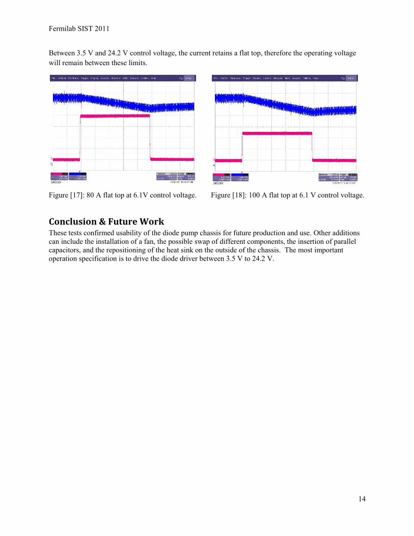
Between 3.5 V and 24.2 V control voltage, the current retains a flat top, therefore the operating voltage will remain between these limits.
Figure [17]: 80 A flat top at 6.1V control voltage. Figure [18]: 100 A flat top at 6.1 V control voltage.
Conclusion & Future Work These tests confirmed usability of the diode pump chassis for future production and use. Other additions can include the installation of a fan, the possible swap of different components, the insertion of parallel capacitors, and the repositioning of the heat sink on the outside of the chassis. The most important operation specification is to drive the diode driver between 3.5 V to 24.2 V.

Fermilab SIST 2011
15
Appendix
A) Circuit Diagram
1
2
3
4
5
6
7
8
9
10
11
12
13
14
15
16
17
18
19
20
21
22
24
25
J8
BNC
12
K1
RELAY 4PDT
3
5
4
6
7
8
9
11
10
12
13
14
1
2
J9
BNC
1
2
D3 FPLED
D2 FP LED
R2 1.3K
R1 1.3K
T1 25.2V AC
1 3
2 5
J7
BNC
1
2
+15VA
+15V
+15VA
+15VA
+15V
A
B
Current Monitor
Pulse Enable
Current Control
AC Line
Filter
+/-15V
200ma
Safety
Contact
Input
110VAC
Safety
+15V
Laser Diode
M1F-SS2.1
x2
Driver
779A
w/Fuse
1165-0250
1475-0530
KHAU-17A16-24
BurndyGOB10-4SNE
J10
Note: +15VA voltage is controlled
by the Safety input contact.
J11
Bulk Power Supply Input
1
2
+15VA
Isolated Analog Interface
EXT-OFF
VMON
Voltage Programming Input
12
12
1, 19
2
2
Isolated Analog Interface
+15VA

Fermilab SIST 2011
16
B) Matlab power_supply_control GUI for Analog control of the Bulk Supply
Interface
A0- Continuation of “Characterization of the Picosecond Pulsed Fiber Laser”
Courtney Clarke
School of Engineering and Applied Science Miami University Oxford, OH 45056
Jinhao Ruan and James Santucci
A0PI Accelerator Division
Fermilab National Accelerator Laboratory Batavia, IL 60510
Summer Internship in Science and Technology (SIST) Program
Date: August 11, 2011
Abstract This report documents the characterization of the Picosecond pulse fiber laser, as it is being commissioned as the seed laser for the RF gun at the New Muon Laboratory. This laser has undergone repair since the summer of 2010, and the downward power trend that was revealed in last year’s power measurements has been fixed. Further testing was done to determine the performance including, the wavelength, mode-locking, pulse spacing, phase noise, and phase shift was measured. The new results reveal ASE issues that will need to be corrected prior to implementation in the New Muon Lab.
2
Table of Contents Abstract ........................................................................................................................................... 1
Introduction ..................................................................................................................................... 3
Background ................................................................................................................................. 3
A0 Photoinjector ...................................................................................................................... 3
New Muon Laboratory ............................................................................................................ 4
Summer 2010 Results .............................................................................................................. 5
Methods........................................................................................................................................... 5
Picosecond Fiber Laser (PSL) ..................................................................................................... 5
Electrical Pulse Generator (EPG) ................................................................................................ 7
Low Dispersion Amplifier (LDA)............................................................................................... 7
Measurements.............................................................................................................................. 8
Power: ...................................................................................................................................... 8
Mode Locking Performance .................................................................................................... 8
Phase Noise.............................................................................................................................. 9
Results & Discussion .................................................................................................................... 11
PSL Results ............................................................................................................................... 11
EPG Results............................................................................................................................... 13
LDA Results .............................................................................................................................. 14
Future Work .................................................................................................................................. 17
Acknowledgements ....................................................................................................................... 17
Works Cited .................................................................................................................................. 18

3
Introduction The A0 Photoinjector (PI) has evolved significantly over the years especially in terms of its RF seed laser. First it was a Nd:YLF passively mode-locked oscillator that required the need of a pulse width compressor. This laser was replaced with a commercially purchased Time-Bandwidth GE-100 IR laser, which is also passively mode-locked, but had a considerably shorter pulse width. This enabled the removal of the compressor region. However, this laser had its own disadvantages including high timing jitter. This resulted in the laser pulses being unequally spaced; therefore this laser could also be upgraded. The laser proposed to replace the GE-100 is the Picosecond Pulsed Fiber Laser by Calmar, which will provide a much decrease jitter for better stability.
Background
A0 Photoinjector
The A0PI houses a 1.3 GHz RF gun and a TESLA test facility (TTF) radiofrequency (RF) cavity. It is used as an R&D physics division, and provides services like its 16 MeV electron linac (1) to many users. It also collaborates with many institutions including Argonne, Cornell, DESY, Lawrence Berkeley National Laboratory (LBNL), the National Institute of Nuclear Physics (INFN), Northern Illinois University (NIU), Rutgers, University of California, Los Angeles (UCLA), University of Chicago, University of Illinois and University of Rochester (2). This research is known as Advanced Accelerator Research and Development (AARD) and A0PI has contributed greatly to accelerator research partnering with the International Linear Collider (ILC) to create a new accelerator research facility called the New Muon Laboratory (NML).
A0 RF gun
Neodymium-doped yttrium-lithium fluoride (Nd:YLF) laser was previously in operation at A0PI. The Nd:YLF laser is passively mode locked and produces 5 ps long pulses at 81.25 MHz. After being amplified, doubled than quadrupled, these now UV pulses hit a CsTe photocathode emitting a 14.8 MeV low emittance electron beam, which is accelerated in a 9-cell superconducting cavity. This beam goes through some beam manipulation to a user experimental area and then a beam dump.

4
Figure [1]: Previous A0PI RF-gun. (3)
New Muon Laboratory
NML will simply be an up-scaled of A0PI with many upgrades. Originally home to a giant Chicago cyclotron magnet, the NML location was remodeled to be an AARD test facility (4). The new NML will provide >40 MeV beam for testing RF cryomodules for Project X and ILC on the low energy end. Some upgrades are scheduled to occur before this move including some beam experiments, instrumentation upgrades, and technology upgrades. Falling under the technology upgrades, the commissioning of the new electron gun will allow for the following advantages:
- lower dark current in the cathode changer and coaxial RF coupler - Longer bunch train length
The reduction of dark current and the lengthening of the bunch train will allow for increased imaging sensitivity, and better control of the pulse train properties.
Furthermore, in NML this 40 MeV electron beam will be accelerated in 3 cryomodules each with eight 9-cell cavities that can generate up to approximately 900 MeV. These cryomodules can be easily installed and removed from the beam line for testing purposes. The injector is proposed to produce a bunch intensity of greater than 3 nC/bunch, a bunch length of less than 300ps, a bunch train length of 3000 bunches at 3 MHz, and a repetition rate of 5 Hz similar to ILC bunches. The facility may also be able to support an approximately 10m diameter ring in the user test area, but

5
this has not yet been finalized (5). Currently, NML is completing the tunnel expansion for the high energy side, but the low energy end is fully operational but beamless. It should be complete by 2012.
Figure [2]: NML underground tunnel expansion of beam line and ring (6)
Summer 2010 Results
During the summer of 2010, the Picosecond Fiber Laser (PSL) was first received for initial testing, but a significant setback stopped tests from proceeding. The power was monitored over certain time periods yielding a significantly decreasing power trend as time increased. This power issue was deemed unacceptable, because the bunch laser needed to be as stable and as constant as possible. The problem was attributed to the electro-optic modulator (EOM), and required the installation of a feedback loop to correct for the power trend (7). As a result, the PSL was sent back to the manufacturers for repair. Recently, it was returned to be re-tested, because the previous issues had been resolved. This report will explain the progress made in the characterization of the PSL after the repair of the laser system, and the new issues that will need to be addressed prior to replacing the GE-100 laser in NML.
Methods
Picosecond Fiber Laser (PSL)
The PSL is potentially a more stable upgrade to the GE-100 laser and it will be the laser used in the New Muon Laboratory as the seed laser for the RF gun. This replacement has to major benefits: longer diode life time and decreased jitter. The PSL unit is proposed to have a diode lifetime of 50,000 hours which is 10 more than the GE-100’s 5000 hours. This will greatly

6
reduced the cost of the system and it will reduce the down time required for the diode replacement.
This upgrade will also enhance the stability by decreasing the jitter in the pulse train. This is important because every fluctuation in the seed laser is reflected in the electron beam. This is why it is extremely crucial that the pulses remain as close to identical as possible in every aspect including pulse width, power, repetition rate, etc. It is also important because when performing tests, if is necessary to keep the environment identical throughout the experiment to reduce the amount of variables. If one aspect of the experiment changes regularly, than there is one more variable to keep track of and could completely alter the results of the test and the thus reducing repeatability. This is especially important when these tests are being done by clients or users who do not maintain the beam themselves.
The final properties of the PSL are listed in Table [1]:
Table [2]:Improvements from implementing the PSL Desired Specifications Value Pulse width 4.9 ps Wavelength 1053.15 nm RF in 1.3 GHz Output power 50 mW
The laser cavity contains a Ytterbium diode fiber amplifier (YDFA). There are some significant advantages that accompany the use of a Ytterbium doped gain medium. Some of these advantages include the ability to amplify pulses to a much higher energy, an effective amplification between about 975 to 1200 nm, high efficiency of output power, wide range of pump wavelengths which allow for the option of being pumped by a diode laser (8). In this case, the YDFA is pumped by 1054 nm. The cavity also houses an output coupler that emits the amplified light, an electro-optic modulator that modulates the losses of the cavity to support mode-locking, and a filter to regulate the linewidth. The pump laser which is a 980 nm diode laser can be manually adjusted via the pump current by turning the knob on the front panel.
Figure [3]: Front Panel of PSL.

7
The pump current and the modulator bias can be set to achieve optimum mode locking. Mode locking is the means by which the laser can create ultra-short periodic pulses (refer to (7) section on mode locking).
Figure [4]: Simplified schematic for the PSL (9).
Electrical Pulse Generator (EPG) The second addition to the upgrade, the electrical pulse generator selects the 81.25 MHz harmonic pulses to progress to the low dispersion amplifier. It also provides pulse width control between 50 to 200 ps, a tunable repetitions rate, an output amplitude from 0.5-7 V, and a very small amount of added jitter (10). Final output power of these selected pulses will be about 1 mW. No issues were encountered when using this device, but the amplifier did create a potential issue that will be addressed later in the report.
Low Dispersion Amplifier (LDA) The low dispersion amplifier is the final addition to the upgraded seed laser system. The desirable specifications of this amplifier include an average power from -3 to 10 dBm (11). The desired output power is about 1 W.
When the 81.25 MHz pulses travel to the amplifier, amplified spotaneous emission (ASE) effects occur allowing for another wavelength of light to be emitted. This ASE light is being amplified along with the 1054 nm pulses, and can increase over time to become a potential danger. The most probable reason for this is because the amplification stage is too long, and ASE has time to develop. Fortunately there are solutions for this issue that will be discussed in the Future Work section.

8
Figure [5]: Actual setup.
Measurements
Power:
The power was the most important measurement that impacted the decision to return the unit back to the manufacturers in 2010. Therefore it was important to measure the power fluctuations this year prior to receiving the PSL. These results were completed during a visit to the company to verify the properties and the results were very promising.
Mode Locking Performance
The PSL is designed to actively mode-lock to longitudinal modes of the laser cavity. Longitudinal modes are the standing wave pattern produced in a cavity with a length that is a multiple of half of the wavelength.
( )
Where L is the length, n is an integer, and is the wavelength. Therefore to lock to one of these modes, one would need a cavity of appropriate length and a phase lock loop to support the achieved mode locking (12). The difference between good and bad mode locking are depicted in

9
Figure [6] and [7]. As shown in these figures, good mode locking displays a narrow spread of sampling points; where as poor mode locking shows a wider spread.
Figure [8]: Good mode locking diode trace. Figure [9]: Poor mode locking diode trace.
For this mode locking task, the laser provides a phase lock loop that receives four inputs locking it to 1.3 GHz: the PZT cavity control, the phase shifter, the modulator bias voltage, and the temperature control.
The phase lock loop controls the length of the PZT cavity for mode-locking. It requires RF and phase shifter inputs. The PZT cavity control adjusts the length of the cavity to the appropriate length for mode locking. The phase shifter adjusts the phase of the RF signal being inputted into the PSL. This should be set to achieve optimum mode locking. The electro-optic modulator (EOM) is controlled via the modulator bias voltage.
The PSL’s EOM modulates the losses of the cavity to support mode-locking. The modulator effectively allows for the destructive interference of modes of the wrong frequency. The EOM consist of a Lithium Niobate (LN) waveguide that can change its refractive properties from an applied voltage. The laser beam travels through the EOM and is split into two, then an RF voltage is applied at 1.3 GHz. When a voltage is applied across the LN, the wave shifts in phase depending on the voltage, therefore when the RF voltage is applied the phases of the separated laser paths shift such that they will interfere to create pulses at the RF frequency (13). The PSL also offer feedback modulator bias control to automatically set the appropriate voltage to be applied on the modulator.
Lastly, temperature fluctuations also have a significant impact on the cavity length, so the PSL implements a temperature control to keep the system regulated at 36 .
Phase Noise
The mode locking process of the PSL is very crucial when attempting to lock to a certain frequency for a pulsed laser. Retaining this lock on the desired mode also deals considerably with the synchronicity between the laser cavity, the RF source, and the modulator. There are

10
many components at A0PI that need to remain synchronized for the production of photoelectrons made for user research. This is the reason why there is a Master “clock” that keeps absolute time in this facility. This is known as the Master oscillator, and it generates a reliable 1.3 GHz signal accessible to many electronics at A0PI.
Though these signals all have access to the reference, the main issue arises from keeping all the signals in tune, and correcting even that slightest of deviations from the master. It is an unfortunate fact that all signals have a tendency to drift in frequency and in phase relative to an absolute, therefore there is always a great necessity to measure and correct for these deviations. Systems that accomplish this are generally called phase lock loops and even lasers, especially pulsed lasers, require this capability when generating uniform pulse trains (14).
The technical term for random deviations from the master signal is jitter. Jitter is a property that needs to be minimized and corrected since it is inherent. In reality, there are always a lot of factors that are causations for jitter. Creating an unstable pulse train causes lower efficiency in pulse production and undefined behavior and properties in the final electrons produced. Therefore the main reason behind minimizing jitter is to keep the setup predictable so the measurements and results are easier to come by and are more reproducible.
Jitter can also be quantified as phase noise over short term measurements. Phase noise is caused by ―random FM and AM modulations (15)‖ on a signal. In relationship to a mode-locking laser like the PSL, phase noise and jitter disrupts the pulse train which can randomly affect the pulse spacing, pulse repetition rate, and pulse width. The laser power gets distributed to other frequencies rather than the desired frequency. Also, since these modulations are randomly distributed around the desired frequency or phase, it can be expressed in term of an average of RMS volts.
Phase Shift Detection
Phase noise can also be quantified by phase shift over a long term scale. The detection technique used at A0PI utilizes a band-pass filter to isolate a 1.3 GHz harmonic of the pulse signal and reads it along with a master 1.3 GHz into a phase detector. The phase detector determines the phase difference between the two signals and applies XOR logic to determine whether or not to emit a signal proportional to the difference of the phase of the two signals. The phase difference at the time of detection is a summation of the initial phase difference and the frequency variation integrated over time and is quantified in mV. Phase noise and phase shift measurements are shown in the results section of this report.
But why was the 16th harmonic of 81.25 GHz tracked rather than 81.25 GHz itself? The reason is for better phase measurement accuracy. At 81.25 MHz there is amplitude noise and phase noise that are indistinguishable. 1.3 GHz has 16 times the accuracy than 81.25 MHz, because it is the fundamental mode of the cavity. Referring to the phase noise measurements in Figures [10] and

11
[11], the RMS volts refers to the amplitude and phase noise rather than just phase noise therefore it is less accurate.
Figure [12]: Phase shift detector from Wilbert Samuel Rossi’s laser phase and jitter study schematic (14).
Results & Discussion
PSL Results
The first and most important test was to determine whether the power issue from 2010 had been resolved and Figure [13] shows the result of this test. The power remained stable over a period of 24 hours so the testing could proceed.
Figure [14]: Power.
The next few tests check the operating conditions of the PSL. Adequate mode locking was achieved prior to each test as verified by the narrow thicknesses of Figures [15] and [20]. Similarly, the wavelength of 1054 nm was verified by Figure [16]. The RMS jitter for the PSL is considerably less than 500 fs which is the jitter in the time bandwidth GE-100 system (Figure [17] and [19]).

12
Figure [15]: PSL diode trace displays a relatively good mode-lock.
Figure [16]: RF spectra center around ~1054 nm.

13
Figure [17]: Phase noise where the RMS jitter is 218 fs. EPG Results
Figure [18]: Pulse trace after EPG (pulse picker), where the time between pulse is ~12 ns or 81.25 MHz.
~12 ns

14
LDA Results
Figure [19]: Phase noise with an RMS jitter of 355 fs.

15
Figure [20]: Pulse trace after LDA displays a mean pulse 376.65256 m, and standard deviation of 3.687m.
Figure [21]: Amplified laser power. Shows very little fluctuations.

16
Figure [22]: Amplified spectrum shows peak at 1054 nm and some ASE peaks to the left of that. After some warm-up time, the phase remain stable with less than 0.6 ps change over 8 hours (Figure [25]). An issue that arises after the light travels through the LDA is ASE. As shown in Figure [22], the spectrum shows a large amount of ASE and unfortunately these effects cannot be ignored. The LDA’s amplified spontaneous emission (ASE) has the potential to increase drastically. This occurs because the amplification stage is too long, and may need to be shortened or amplification reduced. Even though, it is not difficult to dampen the ASE, it will still contribute to noise which is also another unwanted side effect. This is the primary reason why the amplifier unit must be sent back to the manufacturers to correct the problem.

17
Figure [23]: Phase drift displays that it was large over first 3 hours, but then flattens out for the next 8 hours. *conversion 50 mV/ps
Future Work Since the future goal is to move the laser into NML, then tests will continue to be run until then. Most importantly, the LDA has to be fixed and the ASE removed. Only then can final characterization be completed on the finished system. The proposed solution is to pre-amplify the signal prior to the LDA. The amplification stage has too long a duration and ASE develops, but this amplification can be shorted by amplifying in stages. Then the LDA amplification can be reduced and ASE diminished.
Acknowledgements The SIST program has provided a great opportunity and experience that I think many students can benefit from. Special thanks goes out to the SIST coordinators including Dianne Engram, Linda Diepholz, James Davenport, Elliot McCrory, Jamieson Olsen, and Sandra Charles. My SIST mentors David Peterson and Elmie Peoples-Evans were also very helpful during the duration of this internship as well as the entire SIST committee. I would also like to thank my supervisors James Santucci, Jinhao Ruan and the rest of A0PI for taking the time to guide me through my projects and answer any questions I had. Lastly I would like to thank the rest of the summer interns for a great summer!
Ph
ase
dri
ft (
V*)
Time of day (hh:mm am/pm)

18
Works Cited 1. Fliller, Raymond P. Advanced Accelerator R&D at the A0 Photoinjector. Beams Document 3023-v1. [Online] February 6, 2008. [Cited: July 18, 2011.] http://beamdocs.fnal.gov/AD-public/DocDB/ShowDocument?docid=3023.
2. Bellantoni, Leo, Eddy, Nathan and al., et. Proposal for Experiments and Upgrades at the A0 Photoinjector. [Online] November 10, 2008. [Cited: July 18, 2011.] http://beamdocs.fnal.gov/AD/DocDB/0032/003248/001/A0PI_proposal_11_10.pdf.
3. Yang, Xi . Improvement in the laser system for the A0 TTF Photoinjector. [Online] March 10, 2003. [Cited: July 18, 2011.] http://lss.fnal.gov/archive/test-fn/0000/fermilab-fn-0805-ad.pdf.
4. Fermilab. ILCTA – New Muon . ILC-SRF R&D. [Online] [Cited: July 18, 2011.] http://ilc.fnal.gov/accelerators/new_muon.html.
5. Shiltsev, V., et al. Report on Workshop on Future Directions for Accelerator R&D at Fermilab. [Online] May 2009. [Cited: July 18, 2011.] http://lss.fnal.gov/archive/2009/conf/fermilab-conf-09-442-apc.pdf.
6. Church, Mike . Status and Plans for Beams at NML. [Online] December 2, 2010. [Cited: July 18, 2011.] http://beamdocs.fnal.gov/AD/DocDB/0037/003755/001/APC_seminar_church_12_02_10.pdf.
7. Clarke, Courtney. A0- Characterization of the Picosecond Pulsed Fiber Laser. [Online] https://indico.fnal.gov/getFile.py/access?contribId=8&resId=0&materialId=paper&confId=3506.
8. Ytterbium-Doped Fiber Amplifiers. Paschotta, Rudiger, Nilsson, Johan and Tropper, Anne C. 1997, IEEE JOURNAL OF QUANTUM ELECTRONICS, VOL. 33, NO. 7, pp. 1049-56.
9. Calmar Laser. Technology. Calmar Laser. [Online] [Cited: July 18, 2011.] http://www.calmarlaser.com/company/technology.php.
10. —. Electrical Pulse Generator. [Online] [Cited: July 18, 2011.] http://www.calmarlaser.com/docs/EPG.pdf.
11. —. Advanced Products. Calmar Laser. [Online] [Cited: July 18, 2011.] http://www.calmarlaser.com/products/fiber_laser/advanced_products.php.
12. Down, Adrian . 1 Longitudinal modes of a laser cavity. [Online] May 1, 2006. [Cited: July 18, 2011.] http://www.ocf.berkeley.edu/~adriand/classes/files/p110b/37.pdf.
13. Stabilization of electro-optic modulator bias voltage drift using a lock-in amplifier and a proportional-integral-derivative controller in a distributed Brillouin system. Snoddy, Jeffrey, et al. 2007, Appl. Opt. 46, pp. 1482-1485.

19
14. Rossi, Wilbert Samuel. FINAL REPORT _ Wilbert Samuel Rossi _ Fermilab, A0PI. s.l. : Retrieved from A0PI.
15. RF, RFIC & Microwave Theory, Design. www.rfic.co.uk. [Online] [Cited: July 18, 2011.] http://www.ieee.li/pdf/essay/phase_noise_basics.pdf.
16. Ruan, J, et al. Upgrade of the A0 Photoinjector Laser System for NML Accelerator Test Facility at Fermilab. [Online] August 13, 2007. [Cited: July 18, 2011.] http://lss.fnal.gov/archive/2007/conf/fermilab-conf-07-242-ad.pdf.
17. Low Dispersion Amplifier Instruction Manual. Calmar Laser, Inc. Manual No.: Man-880691.
18. Electronic Pulse Generator Instruction Manual. Calmar Laser, Inc. Manual No.: Man-880689.
19. Picosecond Fiber Laser Instruction Manual . Calmar Laser, Inc. Man-880690 V3 .