a treatment of differential signaling and … there any undesirable side effects of length...
TRANSCRIPT

Differential Signaling and Its Design Requirements, Revision 10 Page #1 Copyright Speeding Edge, September 2008
A TREATMENT OF DIFFERENTIAL SIGNALING AND
ITS DESIGN REQUIREMENTS
PREPARED BY SPEEDING EDGE, May 29, 2008 Revised September 9, 2008, Rev 10
AUTHOR: LEE W. RITCHEY
COPYRIGHT, Speeding Edge, April 29, 2008
For use only by clients of Speeding Edge.
WWW.SPEEDINGEDGE.COM
P.O. BOX 2194
GLEN ELLEN, CA 95442

Differential Signaling and Its Design Requirements, Revision 10 Page #2 Copyright Speeding Edge, September 2008
TABLE OF CONTENTS TOPIC PAGE # Introduction………………………………………………………………………………………………..………………3 What is a differential pair and how does it work?.............................................................................................3 Why use differential pairs?..................................................................................................................................4 When are differential pairs needed?...................................................................................................................5 Where are differential pairs commonly used?...................................................................................................5 Why haven’t differential pairs been used for all digital signals?.....................................................................5 How is length matching tolerance determined?................................................................................................6 Are there any undesirable side effects of length mismatching, even when within tolerance?.……………7 Choosing terminator resistor values…………………………………………………………………........................7 When are AC coupling capacitors needed? What do they do? What size should they be?.........................8 Where should AC coupling capacitors be placed? Do they cause signal degradation?...............................8 Are there any downsides to adding AC coupling capacitors to a differential pair?.......................................8 Is tight coupling of a differential pair a good idea?...........................................................................................9 How should differential pairs be routed?.........................................................................................................11 Is a differential impedance specification necessary?.....................................................................................12 Where do return currents flow?.........................................................................................................................12 Does tight coupling eliminate or reduce crosstalk into a diff pair from an aggressor?..............................13 Is broadside routing of differential pairs beneficial?......................................................................................14 Is there a situation where common mode coupling into a differential pair exists?.....................................15 What are the power delivery requirements of differential pairs?...................................................................15 Linear vs. switching power supplies………………………………………………………………………………….16 Separate serdes supplies……………………………………………………………………………………………….16 Do routing vias cause signal degradation in differential signals?.................................................................17 Do right angle bends cause signal integrity problems with high speed differential pairs?........................17 Are there other advantages of differential signaling?.....................................................................................17 Where will differential pairs appear in the future?...........................................................................................18 Are there new sources of signal integrity problems for diff signal as speed increases?...........................18 Summary of design rules for differential signals in a PCB……………………………………………………….18 Summary of rules that do not apply to differential signals routed in a PCB…………………........................18 Hazards to single-ended signals as a result of tightly spaced routing………………………………………...19 Reference materials………………………………………………………...…………………………………………....20 LIST OF FIGURES Figure 1. A typical CMOS differential signaling circuit……………………………..……………………………….3 Figure 2. CMOS differential signaling circuit showing current flow……………………………………………...4 Figure 3. Differential pair routing example and length matching………………………………...……………….6 Figure 4. Overshoot and undershoot…………………………………………………………………………………..7 Figure 5. Test PCB used to measure actual path losses…………………………………………………………...9 Figure 6. Loss vs. frequency for data paths with and without AC coupling capacitors………......................9 Figure 7. Tightly-coupled differential pair eye diagram……………………………………………………………10 Figure 8. Loosely-coupled differential pair eye diagram…………………………………………………………..10 Figure 9. Tightly spaced and loosely spaced differential pairs…………………………………………………10 Figure 10. Differential pair impedance vs. separation………………………………………………....................11 Figure 11. Single-ended impedance vs. separation…………………………………………………….………….11 Figure 12. Differential pair simulation immediately after switching showing currents……………………..13 Figure 13. Worst case cross talk, off center stripline……………………………………………………………..14 Figure 14. Possible ways to route differential pairs near an aggressor…………………………....................14 Figure 15. An unshielded differential pair showing field lines………………………………..…………………15 Figure 16. 3.125 Gb/S eye with ferrite bead in Vdd lead………………………………………….……………….16 Figure 17. 3.125 Gb/S eye with ferrite bead removed from Vdd lead……………………….……………….….16 Figure 18. PCB with seven PS voltages, no ferrite beads…………………………………………………………17
Differential Signaling and Its Design Requirements, Revision 10 Page #3 Copyright Speeding Edge, September 2008
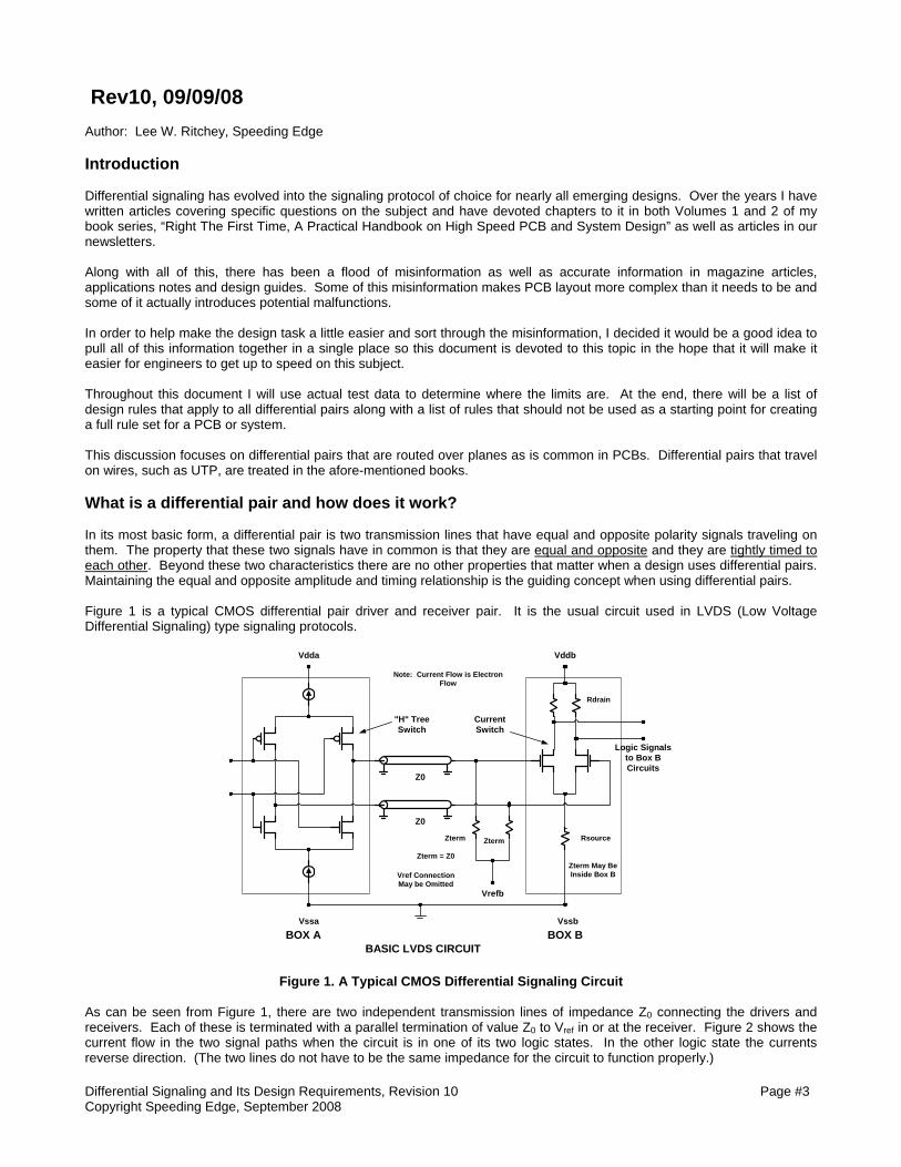
Rev10, 09/09/08 Author: Lee W. Ritchey, Speeding Edge Introduction Differential signaling has evolved into the signaling protocol of choice for nearly all emerging designs. Over the years I have written articles covering specific questions on the subject and have devoted chapters to it in both Volumes 1 and 2 of my book series, “Right The First Time, A Practical Handbook on High Speed PCB and System Design” as well as articles in our newsletters. Along with all of this, there has been a flood of misinformation as well as accurate information in magazine articles, applications notes and design guides. Some of this misinformation makes PCB layout more complex than it needs to be and some of it actually introduces potential malfunctions. In order to help make the design task a little easier and sort through the misinformation, I decided it would be a good idea to pull all of this information together in a single place so this document is devoted to this topic in the hope that it will make it easier for engineers to get up to speed on this subject. Throughout this document I will use actual test data to determine where the limits are. At the end, there will be a list of design rules that apply to all differential pairs along with a list of rules that should not be used as a starting point for creating a full rule set for a PCB or system. This discussion focuses on differential pairs that are routed over planes as is common in PCBs. Differential pairs that travel on wires, such as UTP, are treated in the afore-mentioned books. What is a differential pair and how does it work? In its most basic form, a differential pair is two transmission lines that have equal and opposite polarity signals traveling on them. The property that these two signals have in common is that they are equal and opposite and they are tightly timed to each other. Beyond these two characteristics there are no other properties that matter when a design uses differential pairs. Maintaining the equal and opposite amplitude and timing relationship is the guiding concept when using differential pairs. Figure 1 is a typical CMOS differential pair driver and receiver pair. It is the usual circuit used in LVDS (Low Voltage Differential Signaling) type signaling protocols.
Vdda Vddb
Vssa Vssb
Vrefb
Z0
Z0
BOX A BOX B
"H" TreeSwitch
CurrentSwitch
Logic Signalsto Box BCircuits
BASIC LVDS CIRCUIT
Zterm Zterm
Zterm = Z0
Note: Current Flow is ElectronFlow
Rsource
Rdrain
Vref ConnectionMay be Omitted
Zterm May BeInside Box B
Figure 1. A Typical CMOS Differential Signaling Circuit
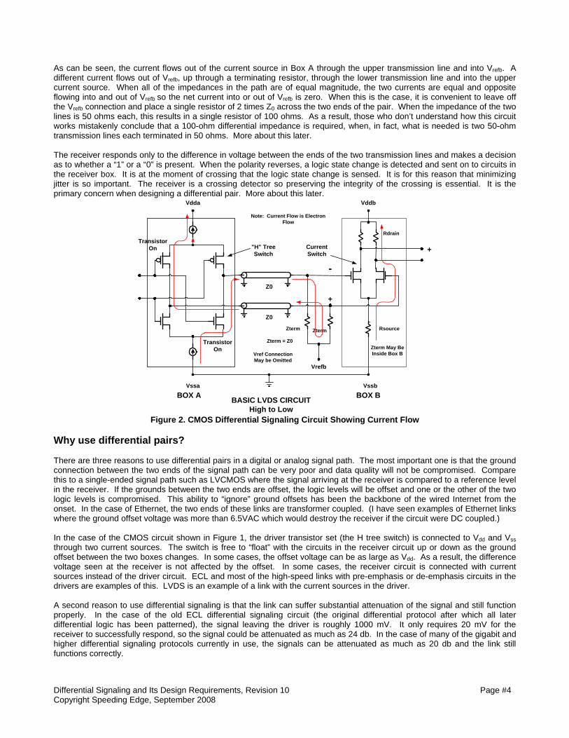
As can be seen from Figure 1, there are two independent transmission lines of impedance Z0 connecting the drivers and receivers. Each of these is terminated with a parallel termination of value Z0 to Vref in or at the receiver. Figure 2 shows the current flow in the two signal paths when the circuit is in one of its two logic states. In the other logic state the currents reverse direction. (The two lines do not have to be the same impedance for the circuit to function properly.)
Differential Signaling and Its Design Requirements, Revision 10 Page #4 Copyright Speeding Edge, September 2008
As can be seen, the current flows out of the current source in Box A through the upper transmission line and into Vrefb. A different current flows out of Vrefb, up through a terminating resistor, through the lower transmission line and into the upper current source. When all of the impedances in the path are of equal magnitude, the two currents are equal and opposite flowing into and out of Vrefb so the net current into or out of Vrefb is zero. When this is the case, it is convenient to leave off the Vrefb connection and place a single resistor of 2 times Z0 across the two ends of the pair. When the impedance of the two lines is 50 ohms each, this results in a single resistor of 100 ohms. As a result, those who don’t understand how this circuit works mistakenly conclude that a 100-ohm differential impedance is required, when, in fact, what is needed is two 50-ohm transmission lines each terminated in 50 ohms. More about this later. The receiver responds only to the difference in voltage between the ends of the two transmission lines and makes a decision as to whether a “1” or a “0” is present. When the polarity reverses, a logic state change is detected and sent on to circuits in the receiver box. It is at the moment of crossing that the logic state change is sensed. It is for this reason that minimizing jitter is so important. The receiver is a crossing detector so preserving the integrity of the crossing is essential. It is the primary concern when designing a differential pair. More about this later.
Vdda Vddb
Vssa Vssb
Vrefb
Z0
Z0
BOX A BOX B
"H" Tree Switch
Current Switch
BASIC LVDS CIRCUITHigh to Low
Zterm Zterm
Zterm = Z0
Note: Current Flow is Electron Flow
Rsource
Rdrain
Vref Connection May be Omitted
Zterm May Be Inside Box B
Transistor On
Transistor On
+
-
+
Figure 2. CMOS Differential Signaling Circuit Showing Current Flow
Why use differential pairs? There are three reasons to use differential pairs in a digital or analog signal path. The most important one is that the ground connection between the two ends of the signal path can be very poor and data quality will not be compromised. Compare this to a single-ended signal path such as LVCMOS where the signal arriving at the receiver is compared to a reference level in the receiver. If the grounds between the two ends are offset, the logic levels will be offset and one or the other of the two logic levels is compromised. This ability to “ignore” ground offsets has been the backbone of the wired Internet from the onset. In the case of Ethernet, the two ends of these links are transformer coupled. (I have seen examples of Ethernet links where the ground offset voltage was more than 6.5VAC which would destroy the receiver if the circuit were DC coupled.) In the case of the CMOS circuit shown in Figure 1, the driver transistor set (the H tree switch) is connected to Vdd and Vss through two current sources. The switch is free to “float” with the circuits in the receiver circuit up or down as the ground offset between the two boxes changes. In some cases, the offset voltage can be as large as Vdd. As a result, the difference voltage seen at the receiver is not affected by the offset. In some cases, the receiver circuit is connected with current sources instead of the driver circuit. ECL and most of the high-speed links with pre-emphasis or de-emphasis circuits in the drivers are examples of this. LVDS is an example of a link with the current sources in the driver. A second reason to use differential signaling is that the link can suffer substantial attenuation of the signal and still function properly. In the case of the old ECL differential signaling circuit (the original differential protocol after which all later differential logic has been patterned), the signal leaving the driver is roughly 1000 mV. It only requires 20 mV for the receiver to successfully respond, so the signal could be attenuated as much as 24 db. In the case of many of the gigabit and higher differential signaling protocols currently in use, the signals can be attenuated as much as 20 db and the link still functions correctly.

Differential Signaling and Its Design Requirements, Revision 10 Page #5 Copyright Speeding Edge, September 2008
A third reason to use differential pairs is for data paths with very high data rates such as gigabit and higher links. It is possible to drive differential paths at rates as high as 10 Gb/S over copper traces in standard PCB materials. This is impossible to do with single-ended logic paths. When are differential pairs needed? The usual conditions where differential pairs are needed can be determined from the characteristics discussed above. These are:
• Where the ground connections between the ends of the signal path are poor. • Where there is significant attenuation along the signal path. • When very high data rates are required.
Where are differential pairs commonly used? The first place where differential signaling was employed was the data paths between the various chassis in early mainframe computer systems. The protocol used was ECL differential signaling. A second place where differential signaling was used was slow speed data links where the environment contained large amounts of electrical noise such as a factory floor. The usual protocol was RS-422 with very large signal swings. Single-ended logic was successfully employed in almost all TTL and CMOS digital applications with wide parallel data buses until laptop computers came onto the scene with a large graphics data stream that had to pass from the motherboard through the hinge to the graphics display. When parallel data paths were used two problems crept in. These were: the wire bundle associated with the wide parallel data bus did not fit well into the hinge and the ground connection was not satisfactory for single-ended operation as the simultaneous switching noise (SSN) was excessive. The solution was to switch to a serial data stream using differential signaling and call the protocol LVDS. Since then, this protocol has been used in an increasingly wider array of products giving rise to the following protocols. All of these protocols share the same characteristics and can use the same design rules. Infiniband Ethernet Hyper Transport PCI Express Fiberchannel XAUI Rocket I/O Firewire IEEE 1394 Universal Serial Bus (USB) SSCSI (serial SCSI) SATA (serial ATA) SIDE (serial IDE) Why haven’t differential pairs been used for all digital signal paths? Knowing all of the advantages of differential signaling, why hasn’t it been adopted for every data path? The reason is that most data streams are parallel bus organized as used by CPUs and memory systems. In order to use a differential data link, which is usually serial, the parallel data stream must be first converted to a serial data stream as it enters the differential pair and then reconverted to a parallel data stream at the receiving end. This is accomplished with serializer/deserializer (serdes). The logic circuits required to do this are relatively complex and, until recently, were costly to implement. As a result, this cost was only justified where no other method of communicating the data was successful. There are examples of single data path signals that require differential signaling even when both ends of the path are on the same PCB. The clocks on DDR2 memory systems are examples of this. The simultaneous switching noise (SSN) associated with large data buses switching cause clocking problems when clocks are single-ended so these clock are differential pairs. With the advent of very large scale integration and the shrinking of features on ICs, it has become possible to manufacture these serdes as part of a large IC at very little cost. This has made it possible to employ serial differential signaling on virtually any product including disc drives (SATA, SIDE and SSCSI), video games, PCs, and peripherals (USB).

Differential Signaling and Its Design Requirements, Revision 10 Page #6 Copyright Speeding Edge, September 2008
How is length matching tolerance determined? At the beginning of this document it was shown that one of the most important design considerations when using differential signaling is making sure that the lengths of the two transmission lines are the same within some limit set by the characteristics of the circuit. A simple solution to the problem is to require that the two paths be length matched “as close as possible” or adhere to some other very tight specification. This solves the problem, but it may result in difficult or impossible routing of the PCB. Designability must also be taken into account in order to arrive at a design that is both routable and functional. A better solution is to understand how length matching affects performance and calculate a length matching tolerance that is, on the one hand, tight enough to guarantee proper performance and on the other hand loose enough to be routable with reasonable effort. There is a straightforward way to do this. Figure 3 depicts an example of routing a differential pair using routing vias to change signal layers. It would be good if this technique could be used without requiring length be added to the shorter side of the pair. A similar condition often exists when entering or exiting connectors. Two examples of signals crossing are illustrated, the upper one with perfect matching and the lower one with the two waveforms skewed. The primary consideration in length matching is keeping jitter to a minimum. Jitter is the movement in time of the crossing or data transition from bit to bit with respect to the clock that is part of the data path. Jitter is at its lowest when the two signals cross in the “straight” parts of the rising and falling edges. The circuit still detects crossings when the waveforms cross as shown in the lower case in Figure 3, but, from cycle to cycle, the crossing will move around in time with respect to the clock due to the uncertainty associated with the low slope of the two waveforms. Crossings will also be detected when the waveforms are skewed even farther than that shown in the lower waveform pair. Because the slope of the waveforms is very near zero, jitter will be very bad and may render the circuit unusable. Knowing this, it is possible to calculate the degree of mismatch that a given circuit can tolerate. This will allow specifying a matching tolerance that balances the demands of performance against ease of layout. The tick marks on the perfectly aligned set of waveforms mark the bounds of the “straight” portion of the switching waveforms. Jitter will stay at its minimum so long as the two edges cross within this time frame. All that is needed is to know the fastest rise and fall times of these waveforms as they arrive at the receiver to perform the necessary calculation. Once this time interval is known, multiplying it by the velocity of the waveforms on the transmission line (usually around 166 pSec per inch in most PCB dielectrics) yields the length tolerance. A couple of examples will illustrate this. LVDS is specified as working properly with length mismatches of 400 pSec. Converting this to a length results in a tolerance of approximately ±1200 mils or ±1.2 inches. Clearly, imposing a length-matching requirement of ±10 mils is excessively tight. Another example is a 2.4 Gb/S serial link often used in high performance products such as routers, switches and servers. The fastest slope at the receiver is 60 pSec in most systems. This results in a length matching tolerance of ±150 mils- enough to allow routing as illustrated in Figure 3 without requiring special length matching. This will result in reduced layout time and congestion of the routing surface that results from the zigzag add length routine usually used for this purpose.
EDGES PERFECTLYLINED UP
EDGES MISALIGNED
EDGES CAN SKEW WITHINLIMITS OF HASH MARKS
WITHOUT JITTER DEGRADATION
EDGES THAT SKEW PAST LIMITOF HASH MARKS WILL HAVE
JITTER DEGRADATION
LENGTH MATCHING TOLEARANCE SHOULDALLOW FOR THIS TYPE OF ROUTING
WITHOUT REQUIRING LENGTH TUNING
LENGTH MISMATCH TOLERANCE
DIFFERENTIAL PAIR LENGTH MATCHING STUDY
Figure 3. Differential Pair Routing Example and Length Matching

Differential Signaling and Its Design Requirements, Revision 10 Page #7 Copyright Speeding Edge, September 2008
Are there any undesirable side effects of length mismatching, even when within tolerance? When the two edges are not aligned so that they don’t cross exactly halfway from one voltage level to the other, as is the misaligned case in Figure 3, there is a short interval of time when current must flow into or out of the Vref terminal. If a single 100 ohm resistor is used instead of two 50 ohm resistors to Vref there is no connection. In this case, current is not available, so one of the edges will be slowed down. For low data rate protocols such as LVDS, this edge degradation is of little consequence. When data rates are high and bit intervals are short, this degradation can have an adverse effect on bit error rate. This is certainly true for 2.4 Gb/S and higher signaling. To solve this problem, a path for the current must be provided. There are several methods for accomplishing this. One is to use a Thevenin termination on the end of each transmission line. This has the unwanted side effect of increasing power consumption and using excessive real estate when done on die. An alternative is to provide the two 50-ohm terminating resistors and connecting their common pins through a very small capacitor to ground. The size of this capacitor need only be on the order of 10 pF for 2.4 Gb/S and higher data rates. This is a practical solution when done on die. (At gigabit and higher data rates, it is necessary to locate the terminations on die in order to preserve signal integrity.) Choosing terminating resistor values It is often the case that terminator values of 110 ohms are used when the specified differential impedance is 100 ohms. This looks like an error, but it is not. It is done on purpose. The reason for the higher value is as follows. Differential signal amplitudes are small, often leaving the driver at 400 mV peak to peak. As a result, there isn’t much noise margin. In order to preserve as much noise margin as possible, it is advisable to make sure that there are no reflections at the receiver from mismatches between the terminator and the line impedance. One way to help this is to use terminator resistor values that are ±1 %. This helps, but the line impedance can vary ±10 % as a normal part of the PCB fabrication process. Figure 4 is the waveform observed at the driver end of a 50-ohm parallel terminated transmission line with a perfect termination and terminations that are mismatched. Notice that when the terminator value is higher than line impedance, in this case 70 ohms, the reflection is in the same direction as the original signal or adds to the incident signal. This is often called overshoot. If there is a reflection, overshoot is the one to have as it does not degrade the signal level. When the terminator value is less than the line impedance, in this case 30 ohms, the reflection is in the opposite direction as the incident waveform or takes away from the incident signal. This is often called undershoot. It is desirable to design the circuit so undershoot does not occur at any time.
Waveforms are driver end of line
50 OHM TRANSMISSION LINE SHOWING EFFECT OF TERMINATING WITH AN IMPEDANCE HIGHER
OR LOWER THAN Zo.
Zt = 70 OHMS
Zt = 30 OHMS
OVERSHOOT
UNDERSHOOT
Zo
Zt
0 Nsec
0 Volts
4.0 Volts
0.5 Volts/Div
20 Nsec
Note: Positive reflections add to waveform. Negative reflections take away from waveform
Figure 4. Overshoot and Undershoot

Differential Signaling and Its Design Requirements, Revision 10 Page #8 Copyright Speeding Edge, September 2008
Since the usual impedance of transmission lines in PCBs is 50 ohms and the tolerance is ±10%, it would be wise to choose a terminator value that is 10% higher than 50 ohms, or 55 ohms. Similarly, for 100-ohm differential impedance, an impedance of 110 ohms would be chosen. In this case, the mismatches will result only in overshoot with an amplitude low enough that it will not cause over-voltage conditions. As can be seen, the 110-ohm value was not an error, rather it was good engineering. As the operating voltages of DDR memory ICs have dropped, the same situation exists. The built in terminations for many of the newer memory ICs is higher than 50 ohms, often 75 ohms. This has been done for the same reason. The number is higher than ±10% due to the fact that resistor tolerances on ICs are often ±20%. When are AC coupling capacitors needed? What do they do? What size should they be? AC coupling capacitors are inserted in series with each leg of a differential pair to provide DC isolation between the two ends of the data path. The usual reason for doing this is because the ground offsets between the two ends of the data path are too large for the built-in current sources in the driver or receiver to deal with. The most common situation where this is likely to occur is when signals travel between boxes or between cards in a large card cage. Many applications notes spell out AC coupling capacitors in paths that begin and end on the same PCB when both ends of the path are the same logic type. This is not necessary and should be avoided. Another example of using AC coupling capacitors is when the two ends of the differential signaling path are different technologies. The most common of these is when LVPECL (low voltage positive emitter coupled logic) is interfaced with LVDS (low voltage differential signaling). Sizing the AC coupling capacitors is done by calculating their capacitive reactance at the lowest frequency data stream that will travel down the path. The capacitive reactance at that frequency needs to be a small fraction of the transmission line impedance to avoid excessive attenuation and signal distortion. For random data patterns, the lowest frequency may be at or near DC, in which case the capacitors will have to have very large values. Luckily, most of the data paths that use differential signaling employ an encoding scheme that makes sure the data stream never drops below some “idling” frequency. This idling frequency is used to recover the clock from the data stream at the receiver end. In this case, the capacitor value can be relatively small. Where should AC coupling capacitors be placed? Do they cause signal degradation? Usually, the transmission lines that are connected to AC coupling capacitors are located on internal layers on the PCB. In order to connect the terminals of the capacitors to the transmission lines a via is required at each end of the capacitor. These vias are almost always through hole vias with a drill diameter of 12 mils. In a 100-mil thick PCB, the parasitic capacitance of each via is approximately 0.4 pF. There is concern that this added parasitic capacitance along with the parasitic capacitance of the capacitor mounting structure might adversely affect the performance of the transmission line. Much has been written about this possibility and much speculation has been done about how severe the effect will be. Similar speculation takes place about where the capacitors should be located. Should they be placed near the driver? Should they be placed midway between the driver and receiver? Should they be placed near the receiver? Many simulations have been done in an effort to determine what effect adding AC coupling capacitors will have with few, if any, real conclusions. A direct approach might be to build identical transmission lines with and without the capacitors and measure the loss vs. frequency of the two paths to see if there is any difference. This is exactly what we have done in order to resolve this confusion. Figure 5 is a photograph of a pair of test PCBs that were used to make these measurements along with others discussed later in this document. Figure 6 is the loss vs. frequency for the two paths from 100 KHz to 6 GHz. This is equivalent to 200 Kb/S to 12 Gb/S. The red curve is the path with no AC coupling capacitors and the blue curve is the path with AC coupling capacitors. Each AC coupling capacitor is 0.1 uF in a 0402 package connected to the transmission line on each side of the mounting pads with 12 mil drilled vias. Notice that there are very small differences between the two curves but nothing that would significantly affect signals out as far as 12 Gb/S. While this test does not actually change the locations of the capacitors along the length of the transmission line, it is reasonable to conclude that since the effect of the capacitor is very small at all frequencies of interest its location along the length of the trace will also not matter. If one considers that this is a linear circuit, the location of the capacitors along the path will not change the overall behavior of the path. Are there any downsides to adding AC coupling capacitors to a differential pair? An obvious downside to adding AC coupling capacitors to a differential pair is the need to find room for the capacitors, their connecting vias and their mounting pads as well as the added parts on the bill of material. A not so obvious downside is that

Differential Signaling and Its Design Requirements, Revision 10 Page #9 Copyright Speeding Edge, September 2008
the receiver side of the path will suffer a DC offset or drift if the data pattern traveling on the path is not symmetrical. There are two solutions to this problem. One solution to this problem is to encode the data in such a way that the data is symmetrical. This is what the 8b/10B encoding does. A second and more general solution is to add a resistive network on the receiver side of the AC coupling capacitor that “biases” the input such that the DC component of a nonsymmetrical of the waveform is eliminated.
Figure 5. Test PCB Used to Measure Actual Path Losses
1 2 3 4 50 6
-30
-20
-10
-40
0
freq, GHz
dB(A
MPH
EN
OL_
CAB
LE_C
APS
_SH
OR
TED
_4PO
RT.
.S(1
,2))
dB(A
MPH
EN
OL_
CAB
LE_4
PO
RT.
.S(1
,2))
Figure 6. Loss vs. Frequency for Data Paths With and Without AC Coupling Capacitors
Is tight coupling of a differential pair a good idea? There is the notion that tight coupling between differential pairs is a good idea. There is even one “guru” who is known to say “everybody knows tight coupling is a good idea” as if one who does not know this must be incompetent. In some cases the reason given is that it reduces unwanted coupling from other signals. This will be discussed later in its own section.

Differential Signaling and Its Design Requirements, Revision 10 Page #10 Copyright Speeding Edge, September 2008
Another reason given is that the “return currents” from one member of the pair will travel better on the other member when tight coupling is done. Figure 7 shows an example of a differential pair tightly routed (5 mil lines and 5 mil spaces with a height above the plane of 10 mils). Figure 8 shows the same differential pair routed with 10 mil spacing. In order to achieve the same “100 ohm” differential impedance, the trace width was increased to 10 mils in the second case. The reason for this will be explained later. Both data paths are running at 3.125 Gb/S and are 30 inches long with copper thickness of ½ ounce or 0.7 mils (18 microns). This method of viewing signal quality is called an eye diagram. It is created by setting up a storage oscilloscope so that one bit period is visible on the screen and then the data path is exercised with thousands of randomly generated data bits. Eventually, the worst-case bit pattern will be captured allowing assessment of the quality of the data path. Notice that the signal amplitude or the eye opening is larger in the loosely coupled case than in the tightly coupled one. The reason for this is higher skin effect loss with the 5-mil trace used in the tightly coupled case. A consequence of crowding traces close to each other is that each trace drives the impedance of the other down due to added parasitic capacitance. Higher parasitic capacitance on a transmission line always drives impedance down. In order to get back to the 50 ohms needed on each trace to meet the 100-ohm differential impedance requirement, the trace must be narrowed resulting in higher skin effect loss. Jitter is also higher in the tightly coupled case. As noted above, one consequence of tight coupling is higher skin effect loss. A second, and more important one is that the two traces must always be kept tightly coupled along their entire length. Figure 9 illustrates what happens to the differential impedance when each of the two pairs in Figures 7 and 8 is separated to weave through a 1 mm pitch BGA or other pin field where it is not possible to maintain the tight spacing.
OSCILLOSCOPEDesign file: DIFFPAIRTIGHTCOUPLING.TLN Designer: Lee Ritchey
BoardSim/LineSim, HyperLynxComment: 10111111111111,2.4GB/S
Date: Monday May 10, 2004 Time: 14:17:14Cursor 1, Voltage = 642.9mV, Time = 274.15psCursor 2, Voltage = 346.3mV, Time = 273.40psDelta Voltage = 296.6mV, Delta Time = 743fs
-0.0
100.0
200.0
300.0
400.0
500.0
600.0
700.0
800.0
900.0
0.000 50.00 100.00 150.00 200.00 250.00 300.00 350.00 400.00 450.00 500.00Time (ps)
Voltage -mV-
Probe 1:U(A0)Probe 2:U(A1)Probe 3:U(C0)Probe 4:U(C1)Probe 5:RS(C0).1Probe 6:RS(C0).2
OSCILLOSCOPEDesign file: DIFFPAIRTIGHTCOUPLING.TLN Designer: Lee Ritchey
BoardSim/LineSim, HyperLynxComment: 10111111111111,2.4GB/S
Date: Monday May 10, 2004 Time: 14:19:05Cursor 1, Voltage = 698.9mV, Time = 274.15psCursor 2, Voltage = 319.2mV, Time = 274.15psDelta Voltage = 379.7mV, Delta Time = 0.000s
-0.0
100.0
200.0
300.0
400.0
500.0
600.0
700.0
800.0
900.0
0.000 50.00 100.00 150.00 200.00 250.00 300.00 350.00 400.00 450.00 500.00Time (ps)
Voltage -mV-
Probe 1:U(A0)Probe 2:U(A1)Probe 3:U(C0)Probe 4:U(C1)Probe 5:RS(C0).1Probe 6:RS(C0).2
Figure 7. Tightly Coupled Differential Pair Figure 8. Loosely Coupled Differential Pair Both differential pairs are spaced 10 mils above the plane over which they are routed. Trace and spacing for Figure 7 is 5 mil lines and 5 mil spaces. Trace and spacing in Figure 8 is 10 mil lines and 10 mil spaces.
Zdiff = 100 OHMS
Zdiff = 100 OHMS
Zdiff = 140 OHMS
Zdiff = 109 OHMS
TIGHTLY COUPLED CASE
LOOSELY COUPLED CASE
TRACE WIDTH 10 MILS SPACING 10 MILS
TRACE WIDTH 5 MILS SPACING 5 MILS
Figure 9. Tightly Spaced and Loosely Spaced Differential Pair

Differential Signaling and Its Design Requirements, Revision 10 Page #11 Copyright Speeding Edge, September 2008
Notice that the differential impedance of the tightly coupled pair increases to 140 ohms when the traces are separated. Said another way, the individual impedance of one trace when separated from its partner is 70 ohms while the loosely coupled pair changes to 109 ohms or a single-ended impedance of 54.5 ohms. The reason the single-ended impedance of the tightly coupled pair is so high when the traces are separated is that introducing any metal, whether a trace or a plane fill, close to a transmission line adds parasitic capacitance resulting in a lowering of the impedance. In order to bring the impedance back to the desired 50 ohms, the trace must be made narrower, in this case to 5 mils. When the metal is removed from the near field, this added parasitic capacitance goes away and the single-ended impedance of the trace returns to 70 ohms. As long as skin effect loss is not an issue, tightly coupled traces work fine. However, it is necessary to maintain the tight coupling along the entire length in order to avoid reflection problems. In many cases this is a severe routing handicap. A restriction that comes to mind is that it will not be possible to route differential pairs through the pin field of a high pin count 1 mm BGA. How should differential pairs be routed? From the above discussion it can be concluded that tightly coupled differential pairs carry with them two handicaps. The first is for a given impedance the traces will have to be narrowed in order to maintain the desired differential impedance. The second is the differential pair must remain tightly coupled along its entire length resulting in routing restrictions that can prove to be a problem. As a result, it is advisable to design a stackup and trace width that meets both the skin effect loss requirements and achieves a differential impedance that results in only minor changes in impedance when the pair must be separated to pass through a tight pin field. The design rule that satisfies the above conditions is a “not closer than” spacing that results in no routing restrictions. The loosely coupled example above is such a “not closer than” case. A big advantage of routing using the “not closer than” rules for differential pairs is that both single-ended traces that are meant to be 50 ohms can use the same trace width as the differential pairs with a “differential impedance” specification of 100 ohms.
Figure 10 Differential Impedance vs. Separation Figure 11 Single Ended Impedance vs. Separation Determining what the “not closer than” spacing must be involves deciding how much impedance variation when differential pairs are separated is acceptable. There isn’t any hard answer, but a rule that is couched in terms of 2H or 3H, H being the height above the plane, is arbitrary. A precise method for arriving at an answer involves using a 2D field solver to calculate the impedance change as the space between the two traces is decreased. I have set a limit of 5% impedance change as acceptable. This is half of the ±10% that the PCB impedance can be expected to vary. I have designed in excess of 100 PCBs using this method with excellent results. Figure 10 shows how differential impedance goes down as the two traces in a pair are moved closer together. Notice that at 10 mil separation the impedance has dropped only 1 ohm or 1%. Figure 11 shows the single-ended impedance of one of the traces in the pair as the two traces are moved close to each other. Notice that with wide separation the impedance is 50 ohms and drops to only 49.5 ohms at 10 mils separation. This why it is reasonable to route single-ended and differential traces using the same trace width so long as separation is maintained. It is also why it is not necessary to measure differential impedance when the “not closer than” rule is followed. The differential pairs in this study are centered stripline spaced 4 mils from either plane using 3313 laminate and prepreg.

Differential Signaling and Its Design Requirements, Revision 10 Page #12 Copyright Speeding Edge, September 2008
Is a differential impedance specification necessary? Nearly all specifications for impedance of differential pairs is for the impedance across the pair. The discussion of how a differential pair works given above shows that the circuit does not depend on a differential impedance. Why, then, is differential impedance always specified? The reason that differential impedance is almost always specified rather than single-ended impedance is that it is thought that differential impedance is different than the sum of the two impedances when the individual impedance is measured from “ground” to either of the two traces. It turns out that it is possible to measure either side of the pair and look for 50 ohms if the differential impedance has been specified at 100 ohms. If the routing instructions are given as “not closer than” as described earlier, it is not even necessary to build a test structure that is a differential pair to get accurate results. Where do return currents flow? Much has been written about where the return currents for a differential pair flow. There is even one text book on high speed design that pictures such a current flow in a differential pair on its cover with current flowing out one side and back in the other. A common assumption is that the return current for one member of the pair flows in the other member. This assumption is based on the fact that the two currents are equal and opposite. This is just a happy coincidence. Referring back to the schematic in Figure 1, it can be seen that each transmission line is a stand alone transmission line that operates independently from the other. They happen to be the same impedance and are terminated in the same impedance, so their currents happen to be equal and opposite. They do not have to be the same impedance for the circuit to work; they just have be properly terminated. If the two currents are independent of each other, where do their return currents flow? It is useful to understand why the currents flow in the first place. The signal integrity issue is concerned with what happens as the logic states change or the transient behavior of the circuits. When a transmission line changes logic states, a current needs to flow to charge up or discharge the parasitic capacitance of the transmission line to alter its voltage. It is reasonable to expect that the two currents, the outbound current and the return current, will flow in the two sides of this parasitic capacitance. When the transmission line is routed by itself this parasitic capacitance exists between the transmission line and the planes over which or between which it travels. If a second transmission line, such as the other member of the differential pair, is routed close to the first one, a small amount of parasitic capacitance will exist between the two lines. For even the tightest routing that is manufacturable, this capacitance is a very small fraction of what exists between the line and the planes, so a tiny amount of the return current would flow in the second transmission line or the partner line. Figure 10 shows the E fields on the top half of the diagram and the current distribution in the traces and planes in the bottom half immediately after the logic state has changed. This is a simulation that shows where the currents are flowing in a differential pair routed between two planes (stripline). Notice that the current distribution in the two traces is crowded near the surface with none flowing in the center of the conductor. This is what is known as skin effect. At very high frequencies the current is crowded near the surface of the conductor due to the rapidly changing magnetic field surrounding the conductor. Also notice that there is an opposite current under each trace in both planes. (Red represents flow in one direction and blue in the other.) These are the return currents for each of the transmission lines. It is flowing there to charge up or discharge the parasitic capacitance between each trace and its plane partners. This simulation was done by Teraspeed using a 2D field solver. It is an animation from which one frame has been taken during the switching event. When the animation is allowed to run to steady state, the currents flow evenly throughout each trace and evenly throughout each plane. This is the “low frequency” behavior of any transmission line. The high frequency behavior shows that the currents crowd near the surface of any conductor and the return currents flow in the “partner” of the transmission line. In this case, the partners are the planes, not the other traces.
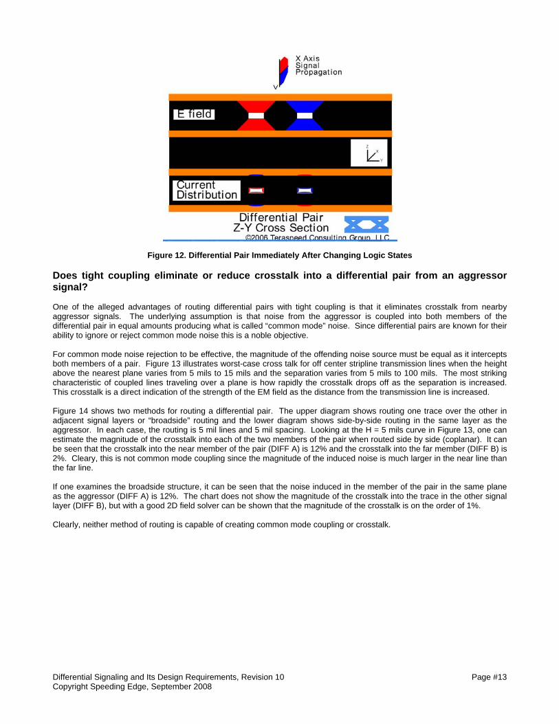
Differential Signaling and Its Design Requirements, Revision 10 Page #13 Copyright Speeding Edge, September 2008
Figure 12. Differential Pair Immediately After Changing Logic States Does tight coupling eliminate or reduce crosstalk into a differential pair from an aggressor signal? One of the alleged advantages of routing differential pairs with tight coupling is that it eliminates crosstalk from nearby aggressor signals. The underlying assumption is that noise from the aggressor is coupled into both members of the differential pair in equal amounts producing what is called “common mode” noise. Since differential pairs are known for their ability to ignore or reject common mode noise this is a noble objective. For common mode noise rejection to be effective, the magnitude of the offending noise source must be equal as it intercepts both members of a pair. Figure 13 illustrates worst-case cross talk for off center stripline transmission lines when the height above the nearest plane varies from 5 mils to 15 mils and the separation varies from 5 mils to 100 mils. The most striking characteristic of coupled lines traveling over a plane is how rapidly the crosstalk drops off as the separation is increased. This crosstalk is a direct indication of the strength of the EM field as the distance from the transmission line is increased. Figure 14 shows two methods for routing a differential pair. The upper diagram shows routing one trace over the other in adjacent signal layers or “broadside” routing and the lower diagram shows side-by-side routing in the same layer as the aggressor. In each case, the routing is 5 mil lines and 5 mil spacing. Looking at the H = 5 mils curve in Figure 13, one can estimate the magnitude of the crosstalk into each of the two members of the pair when routed side by side (coplanar). It can be seen that the crosstalk into the near member of the pair (DIFF A) is 12% and the crosstalk into the far member (DIFF B) is 2%. Cleary, this is not common mode coupling since the magnitude of the induced noise is much larger in the near line than the far line. If one examines the broadside structure, it can be seen that the noise induced in the member of the pair in the same plane as the aggressor (DIFF A) is 12%. The chart does not show the magnitude of the crosstalk into the trace in the other signal layer (DIFF B), but with a good 2D field solver can be shown that the magnitude of the crosstalk is on the order of 1%. Clearly, neither method of routing is capable of creating common mode coupling or crosstalk.

Differential Signaling and Its Design Requirements, Revision 10 Page #14 Copyright Speeding Edge, September 2008
CROSS TALK OFF CENTER STRIPLINE
0
5
10
15
20
25
5 15 25 35 45 55 65 75 85 100
SPACING IN MILS
CR
OSS
TALK
%H= 5 milsH = 10 milsH = 15 mils
H1
S H2
OFF CENTER STRIPLINE STRUCTURE
PLANE
SIGNAL LAYER 1
SIGNAL LAYER 2
PLANE
Figure 13. Worst-case Cross Talk, Off Center Stripline
NEITHER SIDE BY SIDE ROUTING OR ABOVE AND BELOW ROUTING PRODUCES COMMON MODE COUPLING TO A DIFFERENTIAL PAIR
5 mils 5 mils 5 mils 5 mils 5 mils
0.005"
0.015"
DIFF B DIFF A DRIVEN LINE
5 mils
5 mils
5 mils
0.005"
0.015"
DIFF A
DIFF B
DRIVEN LINE
COPLANAR DIFFERENTIAL PAIR CROSS TALK
BROADSIDE DIFFERENTIAL PAIR CROSS TALK
0.005"
CROSS TALK FROMDRIVEN LINE TO DIFF A IS12%. CROSS TALK FROMDRIVEN LINE TO DIFF B IS
1%
CROSS TALK FROMDRIVEN LINE TO DIFF A IS12%. CROSS TALK FROMDRIVEN LINE TO DIFF B IS
2%
Figure 14. Possible Ways to Route Differential Pairs Near an Aggressor
If tight coupling between members of a differential pair does not protect them from crosstalk, what should the routing rules be to avoid crosstalk problems? The only reliable method for controlling crosstalk into a differential pair is to do analysis that establishes the maximum allowable crosstalk into either side of the pair and impose a spacing rule that guarantees this limit is not violated. Is broadside routing of differential pairs beneficial? There are design guidelines that recommend routing differential pairs broadside or one over the other in adjacent signal layers. The usual reasons given for doing this are that tight coupling is good and that common mode noise rejection is better when the pair is routed this way. The benefit of tight coupling was discounted earlier in this paper. From Figure 1 above, it can be seen that there is no beneficial relationship between the pair of transmission lines. Their only relationship is equal and opposite signal amplitudes and tight timing to each other. From Figure 14 it can be seen that neither coplanar routing or broadside routing of a differential pair results in common mode noise rejection due to crosstalk

Differential Signaling and Its Design Requirements, Revision 10 Page #15 Copyright Speeding Edge, September 2008
from an aggressor signal. In fact, if the broadside pair is routed between a Vdd and Vss plane, as is usually the case, there will be differential noise injected into the member of the pair that is routed next to the Vdd layer due to ripple or power supply noise on the power plane. The only way to prevent this is by surrounding the broadside pair with ground layers on both sides which either adds extra layers to the PCB stackup or compromises the PDS system. In addition to the above considerations, broadside routing complicates PCB layout by blocking routing channels in both layers of an adjacent signal layer pair, often forcing the use of more signal layers and increasing the cost of the PCB more than would otherwise be needed. Insuring that the adjacent signal layers are precisely aligned at the PCB fabrication shop is also made more difficult when broadside routing is done. Is there a situation where common mode coupling into a differential pair exists? There must be a case where common mode noise coupling into a differential pair is possible, since so many engineers believe it is possible. Such a case exists. One example is the unshielded twisted pair (UTP) used for virtually all phone wiring as well as for most wired Ethernet. Figure 15 shows a differential pair with the EM fields surrounding each member of the pair. Notice that outside the pair the EM field lines area equal and opposite. As a result, there is no detectable field outside the pair when differential signals are traveling on it. When a source of EM noise is located above or below the pair, the field strength of the EM field is the same amplitude as it intercepts both wires. Any noise coupled into the wires is equal in amplitude and the same polarity. This is the “common mode” noise that is referred to when tight coupling is said to result in common mode noise. When the noise source is located to the right or left of the pair, the strength of the field is slightly less in the member of the pair that is in the shadow of the other member and, as a result, the magnitude of the noise induced into the near wire is larger than the far wire resulting in “differential noise” coupling. True, the difference is not large, but it is measurable. To avoid this problem, the wires are twisted so that one wire is near the noise source for a while and then the other one is (unshielded twisted pair- UTP). Even with the tight coupling of a differential pair suspended in space it is difficult to maintain common mode rejection without twisting the pair. What chance is there to achieve common mode rejection in a PCB when the members of the pair travel over a plane? None.
Figure 15. An Unshielded Differential Pair Showing Field Lines What are the power delivery requirements of differential pairs? A close examination of the circuit in Figure 2 reveals that the current consumed by both the driver and receiver circuits is constant. All than happens when the circuit is active is that the current in either box is simply switched from one side of a circuit to the other as the logic state changes. As a result, the current demand from the power delivery system is constant or “DC”. This means that the power delivery circuit does not need to be very complex if the only circuits being powered are differential drivers and receivers. The power supply could be a simple battery and these circuits would function correctly. Most simple differential driver receiver pairs are relatively insensitive to ripple on Vdd. However, due to the often poor advice on how to design the PDS, large amounts of ripple can be present on Vdd. A common type of ripple or noise on Vdd is switching voltage transients that are generated by DC-DC converters. These voltage spikes often exceed the ratings of the differential circuits resulting in poor signal quality. A common solution has been to insert a ferrite bead in the Vdd lead of the differential driver circuit. As long as the driver is a simple one, as shown in Figure 1, this remedy appears to work. As a

Differential Signaling and Its Design Requirements, Revision 10 Page #16 Copyright Speeding Edge, September 2008
result, the knee jerk solution to poor PDS design is to insert ferrite beads and other components into the power lead of each driver. This has resulted in excessively complex layout problems around FPGAs and other circuits with many differential drivers. A far easier solution to the above problem is to design the PDS in such a manner that the noise transients are not present. The methods for doing this level of design are well documented in the design handbooks mentioned earlier. Most differential drivers used for gigabit and higher differential signaling circuits are not as simple as that shown in Figure 1. They often contain encoding circuits as well as pre-emphasis or de-emphasis circuits in the drivers that are single ended. These circuits require varying current at very high frequencies. Placing ferrite beads in series with their Vdd leads results in severe signal degradation. Figure 16 is the eye diagram measured on a 3.125 Gb/S serial link with a ferrite bead inserted in the Vdd lead of the driver. As can be seen, the eye is severely degraded. This degradation was caused by inserting the ferrite bead in the power lead resulting in a very poor quality source of current for the driver. Figure 17 is the same circuit with the ferrite bead removed. The improvement is dramatic. When the engineer who inserted the ferrite bead was asked why he did it, his answer was that there was excessive noise on Vdd and he hoped the ferrite bead would remove it. It did so, but at the peril of the driver circuit operation. The above is an example of treating a symptom rather than the problem. In most cases, as in this one, the use of ferrite beads in power leads treats a symptom. The symptom in this case is there is too much ripple on Vdd. The cause is a poorly designed power delivery system (PDS). In the first example presented here, the ferrite bead cured the symptom without generating an undesirable side effect. The second example treated only the symptom and introduced a bigger problem.
Figure 16. 3.125 Gb/S Eye With Ferrite Figure 17. 3.125 Gb/S Eye Without Ferrite In summary, simple differential driver receivers can tolerate a relatively poor power delivery system due to the constant current nature of their circuits. Gigabit and higher differential signaling protocols commonly have varying current demands that will be as high in frequency as the signals involved in the signal path. As a result, a PDS design that will supply all of these frequencies is required. Since surface mount bypass capacitors are effective only up to a little more than 100 MHz, it is necessary to have some amount of inter plane capacitance as well. Linear vs. switching power supplies Most FPGA vendors require the use of linear supplies for the high speed serial links that are often a part of their high performance offerings. The reason these are specified is that the authors of the applications notes in which this requirement is contained do not realize that the switching spikes that commonly are part of the output from switching supplies are rather easily suppressed. Many of the switching power supply vendors have applications notes that describe how to deal with these switching transients. Separate Serdes supplies The same vendors that specify linear-only supplies for their Serdes also require a separate supply voltage for them even though other parts of the FPGA use the same voltage. The reason for doing this is to prevent “noise” from other parts of the design from coupling into the Serdes. The solution to this problem is to design a single supply that has ripple or noise which is within the tolerance of all the circuits being powered. Most vendors do not know what the noise tolerance is of their serdes

Differential Signaling and Its Design Requirements, Revision 10 Page #17 Copyright Speeding Edge, September 2008
so this complicates doing an adequate design. From experience it can be said that virtually all Serdes on the market at present are capable of withstanding as much as 50 mV of ripple without noticeable degradation. This is a target that is readily obtainable with standard capacitors. Figure 18 is a 22-layer PCB with one 1152 pin FPGA in the center that has all of its Serdes used as well as 200+ single-ended I/O. It also has two 10 Gb/S ports in the lower right corner and two 1 Gb/S ports in the upper right hand corner. It has no ferrite beads in any supply and the Serdes supply voltage is shared with other parts of the FPGA. Each supply voltage impedance was designed to be 10 mOhms or less from DC to 150 MHz with 10 or more nF of plane capacitance for each supply. When the system is running at full traffic, there is no measurable ripple on any of the seven supplies.
Figure 18. PCB With Seven PS Voltages, No Ferrite Beads Do routing vias cause signal degradation in differential signals? In the context of this question, a routing via is any via used to connect a component lead to an internal layer or to allow a signal to change layers. These vias usually have a drill diameter of 12 mils and add a parasitic capacitance of about 0.5 pF to the trace where they connect in a PCB that is 100 mils thick. A common restriction placed on routing “high speed” traces is that no vias are allowed for fear that they will degrade the signal. This has the effect of constraining routing to a single layer of the PCB- often a severe restriction that forces the use of more signal layers than might actually be needed. The signals in Figure 6 have two or four vias along their length. As can be seen, the loss vs. frequency of the two paths is virtually the same and linear indicating that adding routing vias does not have a notable effect on the signal path. (The plated through holes required by press fit connectors are much larger and, as a result, have substantially more parasitic capacitance and can have an adverse effect on the signals at high frequencies.) One exception to the above explanation is the case of a four-layer PCB such as a PCB used for a PC motherboard. In this case, when the via is used to transition from the top signal layer to the bottom signal layer, there is no easy path for the return current and there will be signal degradation. The degradation does not stem from the via itself, but from the act of layer changing. To avoid this problem on a four-layer PCB, the signals must start and end on the same signal layer and not pass through to the other signal layer. Do right angle bends cause signal integrity problems with high speed differential pairs? This is another of the many issues that worry design engineers. Many of the applications notes and design guides for differential signaling, as well as single-ended signaling, prohibit the use of right angle bends for fear they will degrade the signals. The origin of the rule prohibiting the use of right angle bends is covered in Chapter 25 of Volume 1 along with measurements that show right angles in traces to be invisible to at least 20 GHz. References 16 and 20 of the bibliography are additional studies that show right angle bends are not to be feared in logic designs. Are there other advantages of differential signaling? As noted earlier, the equal and opposite nature of the differential pair means that demands on the PDS are less than for a similar single-ended data path. This has a significant benefit when passing signals into and out of IC packages. Much has been written about simultaneous switching noise (SSN) of wide, single-ended buses and the signal integrity problems

Differential Signaling and Its Design Requirements, Revision 10 Page #18 Copyright Speeding Edge, September 2008
associated with Vdd and ground bounce in IC packages. Often, this limits the width of parallel data buses or forces the total redesign of IC packages to reduce SSN as the rise and fall times of the signal get faster. Replacing wide, parallel buses with high data rate differential links solves this problem. Another benefit of differential signaling, again, because of the equal and opposite nature of the two signals, is the reduction or elimination of EMI when signals must travel on cables or flexible circuits. This is the fundamental reason that fast Ethernet does not cause an EMI problem even though the signals are traveling on an unshielded twisted pair. The connection between a laptop motherboard and the display is another place where this property is used, as are differential connections between PC mother boards and disc drives. Where will differential pairs appear in the future? DDR memory buses have become quite large; often as many as 130+ single-ended address and data paths are used. Simultaneously, these paths have increased in speed and their rise and fall times have become very small (less than 200 pS). This has resulted in severe problems with SSN. The current speeds of DDR2 are reaching the limits of what can be done to increase bandwidth of the memory subsystem to keep pace with the increase in CPU speeds. The DDR standards body is working on a memory architecture that is based on converting the wide parallel data buses to very high speed differential paths. This is possible at a reasonable cost due to the reduction in the cost of creating serdes to get back and forth between serial and parallel data streams. This new memory architecture is in the prototype stages at the present time. Are there new sources of signal integrity problems for differential signals as speed increases? In addition to signal degradation from reflection and crosstalk, there can be signal attenuation stemming from skin effect losses and losses in the dielectric used to fabricate the PCB. The frequency or data rate at which these losses become a factor depend on the highest frequency in the data stream, the length of the path and the type of dielectric material used. There is a desire in some quarters to have a simple rule of thumb that allows easy determination of when the speed is fast enough that these losses need to be accounted for. This would certainly be handy. Unfortunately, the problem is too complex for such an easy solution. The only way to be certain that these two sources of degradation are not going to be a problem is by using a good signal integrity analysis tool to simulate the actual proposed path with the materials and signals to be used. This analysis is not difficult to perform and is an integral part of good systems engineering. As speeds exceed 2 Gb/S there is another potential source of signal degradation that is difficult to isolate. This degradation shows up as excessive jitter on the receive signal and skew between the two sides of the differential pair. The source of this degradation is the irregular weave of the glass used in the laminate. There are at least two weaves, 106 and 1080 that cause this problem. This is discussed at length in Volume 2 of the book set mentioned at the start of this document and in reference 18 in the bibliography at the end of the document. Summary of design rules for differential signals routed in a PCB
• Members of a differential pair do not have to be routed together. • Members of a differential pair should be routed to a “not closer than” rule. • Vias in differential pairs are not harmful. • Right angle bends in differential pairs are not harmful. • AC coupling capacitors may be placed anywhere along the length of the pair. • Length matching tolerance of a differential pair is determined using rise time at the receiver. • Specifying the single-ended impedance of each member of a differential pair is acceptable. • Parallel terminations of differential pairs should be sized on the high side of the PCB trace impedance tolerance. • Crosstalk spacing rules must account for the fact that there is no common mode noise rejection in a PCB. • Broadside routing of differential pairs makes PCB layout more difficult than coplanar routing. • Broadside routing of differential pairs makes PCB fabrication more difficult than coplanar routing.
Summary of rules that do not apply to differential signals routed in a PCB
• The return current for one member of a differential pair flows in the other member. • Ferrite beads should be placed in the Vdd leads of differential drivers. • Differential impedance is a necessary requirement for differential signaling. • Broadside routing of differential pairs results in signal integrity improvements.

Differential Signaling and Its Design Requirements, Revision 10 Page #19 Copyright Speeding Edge, September 2008
Hazards to Single-ended Traces Due to Tight Routing While this topic is not directly related to differential signaling it is useful to examine how single-ended traces interact when routed tightly. All transmission lines interact with each other when they are placed close to each other whether they are on the same plane or an adjacent plane. In few, if any, cases including differential signaling discussed in this paper, is this interaction beneficial. Two effects of interaction that are not beneficial are crosstalk and reduction in impedance. A common routing density left over from the time when impedance and crosstalk were unimportant due to the relatively slow rise times of signals produced by such logic at TTL or slow CMOS circuits is 5 mil lines and 5 mil spaces. Figure 13 shows how crosstalk increases as traces are routed ever closer together. For a 5 mil line 5 mil space routing strategy in a stripline layer with a height above the plane of 5 mils, the cross talk is 12%. Few logic families have enough noise margin to tolerate the level of crosstalk. Another potentially damaging side effect of this routing density is shown in Figure 11 “Single Ended Impedance vs. Separation” to other traces routed in the same layer. Notice for a 50 ohm trace when the separation is 10 mils or more, the single ended impedance of a trace is little affected by neighboring traces. When the spacing is reduced to 5 mils, the impedance drops to 46.5 ohms a 7% drop from what was expected. The reason that this happens is related to the fact that any metal introduced into the near field of a transmission line increases the parasitic capacitance per unit length of that transmission line. Increased parasitic capacitance on a transmission line results in a powered impedance. When a second transmission line is added to the other side of the pair described in the previous paragraph the impedance of the line in the center is driven to about 42 ohms or an error of almost 16%- much larger than the tolerance specification placed on the PCB manufacturer. Such large changes in impedance compromise the entire reflection budget of most logic families. The effects of this impedance variation is most visible when a trace is routed for part of its length parallel to one or more traces and then travels by itself for some distance. The 50 ohms measured on a stand-alone test trace can be reduced to a far lower value on signal traces. From the above, it follows that routing rules for single ended traces should be similar to those for differential signals. A “not closer than” routing specification must be imposed to insure that impedance variations along the length of a routed trace are within signal integrity limits.

Differential Signaling and Its Design Requirements, Revision 10 Page #20 Copyright Speeding Edge, September 2008
Reference materials
1. Child, Jeff, “Low-Voltage Differential Signaling (LVDS) Reports for Duty” Electronic Design. May 25, 1998.
2. Ritchey, Lee W, “ How to Design a Differential Signaling Circuit.” Printed Circuit Design, March 1999.
3. Crisafulli, Kellee & Kaufer, Steve, “Terminating Differential Signals on PCBs.” Printed Circuit Design, March 1999.
4. EDN Staff, “Line Drivers/Receivers Conform to New LVDS Standards” EDN, June 10, 1999.
5. Johnson, Howard, “Differential Termination” EDN, June 5, 2000.
6. Desposito, Joseph, “Transceiver Chip Replaces Parallel Backplanes with High-Speed Serial Links”
Electronic Design, February 7, 2000.
7. Goldie, John & Nicholson, Guy, “A Case for Low Voltage Differential Signaling as the Ubiquitous Interconnect Technology” Electronic Systems, March 1999.
8. Rothermel, Brent R, etal, “Practical Guidelines for Implementing 5 GB/S in Copper Today, and a Roadmap
to 10 GB/S” DesignCon2000.
9. Cohen, Tom, etal, “Design Considerations for Gigabit Backplane Systems” DesignCon2000.
10. Patel, Guatam, etal, “Gigabit Backplane Design, Simulation and Measurement” DesignCon2001.
11. Bogatin, Eric, “The Return Current in a Transmission Line”, PCB Design, Aug 2002.
12. Bogatin, Eric, “When Should I Worry About Lossy Lines?” Printed Circuit Design and Manufacture, March 2005.
13. Bogatin, Eric, “A Designer’s Guide to High Speed Serial Links”, Printed Circuit Design, June 2005.
14. Clink, James, “Maximizing 10 GB/S Transmission Paths in Copper Backplanes”, DesignCon 2003, January
2003.
15. Johnson, Howard, “Modeling Skin Effect Loss”, EDN, April 2001.
16. Johnson, Howard, “Who’s Afraid of the Big, Bad Bend? Right Angle Turns”, EDN, May 2000.
17. Johnson, Howard, “Differential Signaling, Measuring Differential Impedance”, EDN, January 2000
18. Bogatin, Eric, “Skewering Skew, Laminate Weave Induces Skew”, Printed Circuit Design, April 2005.
19. Theorin, etal, “Differential TDR Testing Techniques”, W. L. Gore, March 1998.
20. Brooks, Douglas. “90 Degree Corners, The Final Turn.” Printed Circuit Design. January 1998.
21. Brist, Gary etal, “Non-classical conductor Losses Due to Copper Foil Treatment”, Circuitree, May 2005.