a study of the memristor the fourth circuit element - k-rex home page
TRANSCRIPT

A STUDY OF THE MEMRISTOR,
THE FOURTH CIRCUIT ELEMENT
by
KETAKI KERUR
B.E., Visvesvaraya Technological University, 2007
A REPORT
submitted in partial fulfillment of the requirements for the degree
MASTER OF SCIENCE
Department of Electrical and Computer Engineering
College of Engineering
KANSAS STATE UNIVERSITY
Manhattan, Kansas
2010
Approved by
Major Professor
Dr. Stephen A. Dyer

Abstract
Every person with an electronics background will be familiar with the three fundamental circuit
elements — the resistor, the capacitor, and the inductor. These three elements are defined by the
relation between two of the four fundamental circuit variables — current, voltage, charge and
flux. In 1971, Leon Chua reasoned on the grounds of symmetry that there should be a fourth
fundamental circuit element which gives the relationship between flux and charge. He named
this circuit element the memristor, which is short for ―memory resistor.‖ In May 2008,
researchers at HP Labs published a paper announcing a model for the physical realization of the
memristor.
This report focuses on the memristor and reviews its properties. The HP model for the memristor
is also discussed, and its behavior is studied through simulations. A few of the potential
applications of the memristor are presented.

Acknowledgments
Many minds and hands have contributed to the successful completion of this research. This
research gave me an opportunity to learn from some of the best minds.
First, I would like to thank my major advisor, Dr. Stephen A. Dyer for acting as a guiding light
throughout the course of this research. Dr. Dyer was there to help me whenever I needed it in
spite of his busy schedule. I would also like to thank him for suggesting such an interesting topic
for my research.
I am grateful to Dr. Andrew Rys for agreeing to be a committee member and advising me on this
work. Dr. Rys has been a constant source of encouragement.
I would like to express my sincere gratitude to Dr. Medhat Morcos for agreeing to be on my
committee. Dr. Morcos has been inspirational and I thank him for his continued support.
I am extremely grateful to Dalibor Biolek, member of the CAS/COM Czech National Group of
IEEE, and the president of Commission C of the URSI National Committee for Czech Republic,
for answering my queries through email and helping me with the simulations.
I would also like to take this opportunity to thank my parents, Mrs. Rashmi Kerur and Mr. Ram
Kerur, and my friends for their invaluable support and motivation.

Dedication
Dedicated to my family and friends
for their unconditional love and support.
v
Contents
List of Figures .............................................................................................................................................. vii
Chapter 1: Introduction ................................................................................................................................ 1
1.1Structure of the Report ........................................................................................................................ 2
Chapter 2: Historical Background ................................................................................................................. 3
Chapter 3: Memristor Theory ....................................................................................................................... 5
3.1 Origin of the Memristor ...................................................................................................................... 5
3.2 Definition of a Memristor ................................................................................................................... 7
3.3 What is Memristance? ........................................................................................................................ 8
3.4 Analogy of a Memristor ...................................................................................................................... 8
3.5 Properties of a Memristor .................................................................................................................. 9
3.5.1 – Curve of a Memristor .......................................................................................................... 9
3.5.2 Current–Voltage Curve of a Memristor ....................................................................................... 9
3.6 Memristive Systems .......................................................................................................................... 10
Chapter 4: Model of the Memristor from HP Labs ..................................................................................... 12
4.1 Linear Drift Model [9]........................................................................................................................ 14
Chapter 5: Results and Simulations ............................................................................................................ 17
5.1 SPICE Model [21] ............................................................................................................................... 17
5.2 Simulation Results— Using SPICE model .......................................................................................... 18
5.2.1 Simulations for a Memristor Driven by Voltage using PSPICE .............................. 18
5.3 Simulation Results— Using MATLAB ................................................................................................ 22
5.3.1 Simulations for a Memristor Driven by Voltage using MATLAB ........................... 22
Chapter 6: Potential Applications of Memristor ......................................................................................... 25
6.1 Two-state Charge-controlled Memristor [16] ................................................................................... 25
6.2 Digital Logic Implementation Using Memristor ................................................................................ 25
6.2.1 Memristor as a Logical State Element [22] ................................................................................ 25
6.2.2 Inverting Configuration [22] ....................................................................................................... 26
6.2.3 NAND Operation [22] ................................................................................................................ 27
6.3 Arithmetic Processing Using Memristors .......................................................................................... 28
6.3.1 Memristor Crossbar ................................................................................................................... 28

vi
6.3.2 Arithmetic Processing [24] ......................................................................................................... 29
6.4 Memristor Memory .......................................................................................................................... 31
Chapter 7: Conclusion and Future Research ............................................................................................... 32
7.1 Conclusion ......................................................................................................................................... 32
7.2 Future Research ................................................................................................................................ 32
References .................................................................................................................................................. 34
Appendix ..................................................................................................................................................... 38
MATLAB Code for Memristor Simulation ............................................................................................... 38
SPICE Listing for Memristor Simulation [21] ........................................................................................... 39

vii
List of Figures
Fig. 1. Four basic circuit elements (Adapted from [1]). ................................................................................ 1
Fig. 2. The three circuit elements defined as a relation between four circuit variables (Adapted from [16]).
...................................................................................................................................................................... 5
Fig. 3. Aristotle's theory of matter (Adapted from [16]). .............................................................................. 6
Fig. 4. The four fundamental two-terminal circuit elements (Adapted from [16]). ...................................... 6
Fig. 5. Symbol of the memristor (Adapted from [5]). .................................................................................. 7
Fig. 6. Typical – curves of memristors(Adapted from [16]). .................................................................. 9
Fig. 7. The pinched hysteresis loop and the loop shrinking with the increase in frequency (Adapted from
[18]). ........................................................................................................................................................... 10
Fig. 8. Schematic of HP memristor (Adapted from [9]). ............................................................................ 12
Fig. 9. Behavior of HP memristor when positive and negative voltages are applied (Adapted from [20]).
.................................................................................................................................................................... 13
Fig. 10. Structure of the SPICE model (Adapted from [6]). ....................................................................... 17
Fig. 11. An input voltage applied to the memristor. .................................................................. 18
Fig. 12. Waveform of the current through the memristor. .................................................................. 19
Fig. 13. Voltage across the capacitor which gives the internal state of the device. ............................... 19
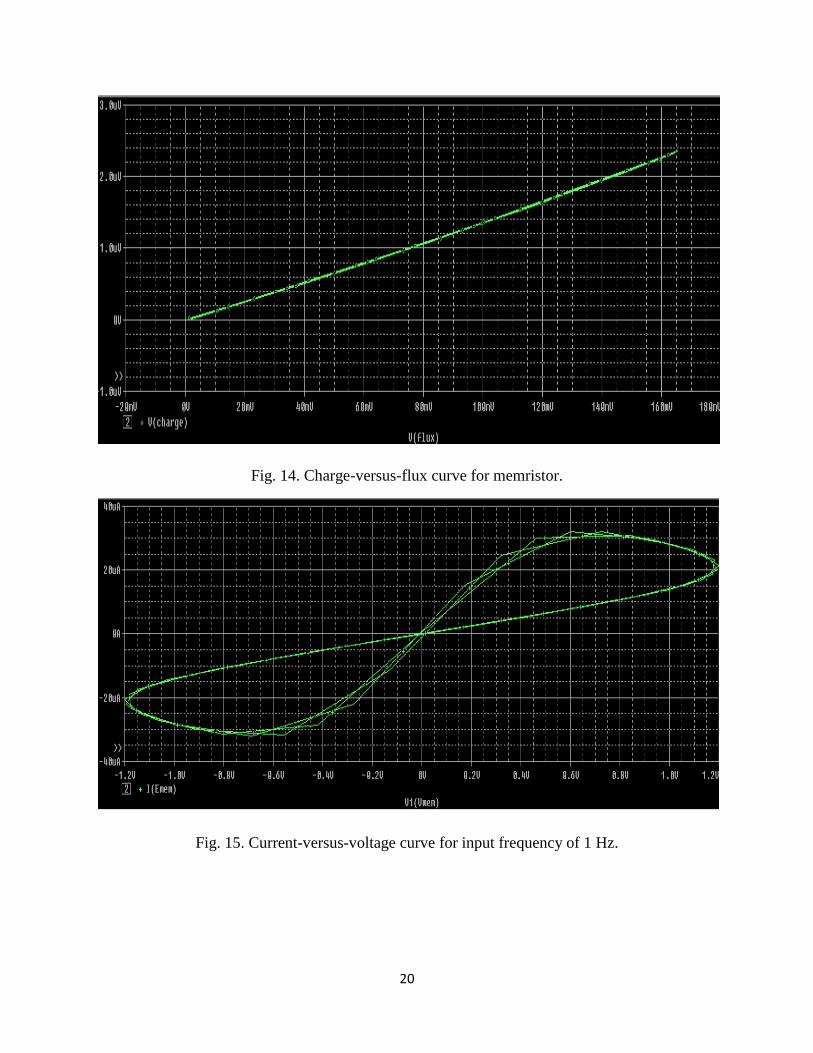
Fig. 14. Charge-versus-flux curve for memristor........................................................................................ 20
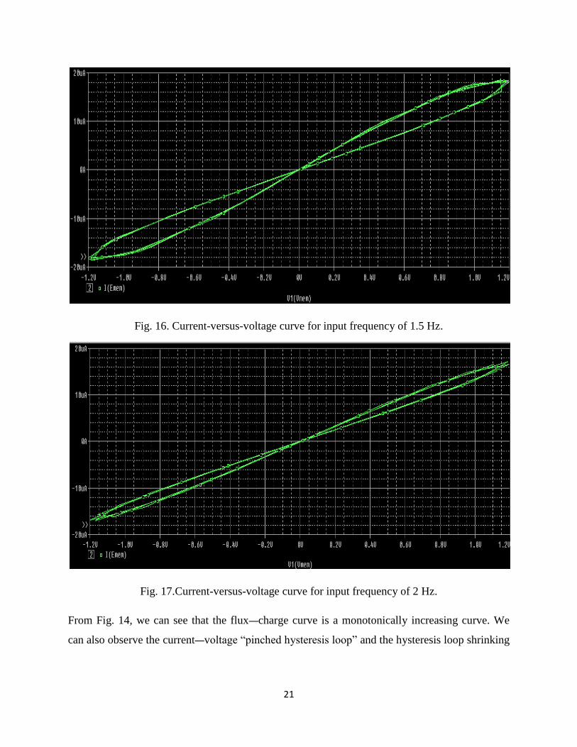
Fig. 15. Current-versus-voltage curve for input frequency of 1 Hz. ........................................................... 20
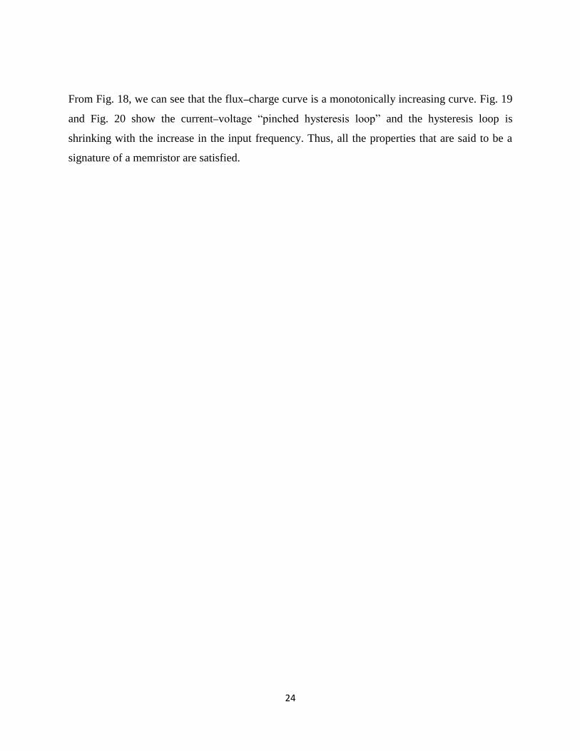
Fig. 16. Current-versus-voltage curve for input frequency of 1.5 Hz. ........................................................ 21
Fig. 17.Current-versus-voltage curve for input frequency of 2 Hz. ............................................................ 21
Fig. 18. Plot of flux versus charge. ............................................................................................................. 22
Fig. 19. Plot of current versus voltage for ω = 3 rad/s. ............................................................................... 23
Fig. 20. Plot of current versus voltage for ω = 8 rad/s. ............................................................................... 23
Fig. 21. – curve of a two-state charge-controlled memristor ................................................................. 25
Fig. 22. Memristor as a state element (Adapted from [22]). ....................................................................... 25
Fig. 23. Inverting configuration of two memristors (Adapted from [22]). ................................................. 26
Fig. 24. Wired- AND logical implementation (Adapted from [22]). .......................................................... 28
Fig. 25. Memristor Crossbar Array (Adapted from [23]). .......................................................................... 28
Fig. 26. Memristor crossbar array which includes a horizontal wire intersected by eight vertical wires
(Adapted from [24]). ................................................................................................................................... 29
Fig. 27. Memristor crossbar array as an arithmetic processor (Adapted from [24]). .................................. 30

viii
Fig. 28. Symbol of memcapacitor and meminductor (Adapted from [27]). ............................................... 32

1
Chapter 1: Introduction
In circuit theory, the three basic two-terminal devices — namely the resistor, the capacitor and
the inductor — are well understood. These elements are defined in terms of the relation between
two of the four fundamental circuit variables, namely, current , voltage , charge and flux .
The current is defined as the time derivative of the charge . According to Faraday‘s law, the
voltage is defined as the time derivative of the flux . A resistor is defined by the relationship
between voltage and current , the capacitor is defined by the relationship between
charge and voltage and the inductor is defined by the relationship between flux and
current . Out of the six possible combinations of the four fundamental circuit
variables, five are defined. In 1971, Prof. Leon Chua proposed that there should be a fourth
fundamental circuit element to set up the relation between charge and magnetic flux and
complete the symmetry as shown in Fig. 1.
Fig. 1. Four basic circuit elements (Adapted from [1]).
Resistor
Capacitor
Inductor
Memristor
2
Prof. Leon Chua named this the memristor, a short for ―memory resistor.‖ The memristor has a
memristance and provides a functional relation between charge and flux . In 2008,
Stanley Williams, et al., at Hewlett Packard, announced the first fabricated memristor.
This report focuses on the memristor and reviews its properties and applications. The model of
the memristor from HP Labs and simulations showing the behavior of this memristor model for
different input voltages are included in this report. The simulations are carried out using PSPICE
and MATLAB.
1.1 Structure of the Report
Chapter 2 gives a brief description of the historical background of the memristor. Chapter 3
presents the theory and properties of the memristor. The HP model for the memristor is described
in Chapter 4. Chapter 5 gives the results of the simulations. The potential applications of the
memristor are described in Chapter 6. Finally, Chapter 7 provides a conclusion and a brief
insight regarding possible future work.

3
Chapter 2: Historical Background
The concept of a resistor with memory existed even before Leon Chua‘s publication on the
memristor in 1971. In 1960, Prof. Bernard Widrow of Stanford University developed a new
circuit element named the ―memistor.‖ The memistor was a three-terminal device for which the
conductance between two of the terminals was controlled by the time-integral of the current into
the third terminal. Thus, the resistance of the memistor was controlled by charge. Memistors
formed the basic components of the neural-network architecture called ADALINE (ADAptive
LInear NEuron).
In 1968, F. Argall published a paper, ―Switching phenomena in titanium oxide thin films,‖ which
shows results similar to that of the memristor model proposed by Stanley Williams and his team.
In 1971, Leon Chua mathematically predicted [2] that there is a fourth fundamental circuit
element characterized by a relationship between charge and flux linkage.
In 1976, Leon Chua and Sung Mo Kang published a paper entitled ―Memristive devices and
systems‖ [3], generalizing the theory of memristors and memristive systems.
In 1990, S.Thakoor, et al., [4] demonstrated a tungsten-oxide variable- resistance device that is
electrically reprogrammable. It is not clear whether the memistor device described has any
relation with Chua‘s memristor [5].
Four years later, in 1994, Buot and Rajgopal published an article entitled ―Binary information
storage at zero bias in quantum-well diodes‖ [6]. The article described current–voltage
characteristics similar to that of the memristor in AlAs/GaAs/AlAs quantum-well diodes. The
analysis showed no direct connection to Chua‘s memristor [5].
In 2000, Beck, et al., of IBM‘s Zurich Research Laboratory, described reproducible resistance
switching effects in thin oxide films [7]. The hysteretic features of these switches are similar to
those of the memristor.
In 2001, Liu, et al., researchers in the Space Vacuum Epitaxy Center of the University of
Houston, presented results [8] during a non-volatile memory conference held in San Diego,
California, showing the importance of oxide bilayers to achieve high-to-low resistance ratio.

4
Apart from the devices mentioned above, it is interesting to note that between 1994 and 2008
there were many other devices developed with behavior similar to that of the memristor, but only
the HP scientists were successful in finding a link between their work and the memristor
postulated by Chua [9].
In 2008, thirty-seven years after Leon Chua‘s proposal, the memristor in device form was
developed by Stanley Williams and his group in the Information and Quantum Systems (IQS)
Lab at HP. Dmitri Strukov, Gregory Snider, Duncan Stewart, and Stanley Williams, of HP Labs,
published an article [10] identifying a link between the two-terminal resistance switching
behavior found in nanoscale systems and Leon Chua's memristor. The model proposed by them
is described in detail in Chapter 4 of this report.
Victor Erokhin and M. P. Fontana claimed to have developed a polymeric memristor [11] before
the titanium-dioxide memristor developed by Stanley Williams‘ group.
Since the announcement of the break through by Stanley Williams‘ group, numerous papers with
the aim to analyze the elementary attributes of the memristor and memristor applications in
various areas of circuit design have appeared.
Later in 2008, J. Joshua Yang, Matthew D. Pickett, Xuema Li, Douglas A. A. Ohlberg, Duncan
R. Stewart and R. Stanley Williams published an article [12] demonstrating the memristive
switching behavior and mechanism in nanodevices.
In October 2008, Yu V. Pershin, S. La Fontaine, M. Di Ventra published an article [13]
identifying memristive behavior in amoeba's learning.
In January 2009, Sung Hyun Jo, Kuk-Hwan Kim, and Wei Lu of the University of Michigan
published an article [14] describing an amorphous-silicon–based memristive material capable of
being integrated with CMOS devices.
In June 2009, scientists at NIST [15] reported that they had fabricated nonvolatile memory using
a flexible memristor that is both inexpensive and low-power.
5
Chapter 3: Memristor Theory
3.1 Origin of the Memristor
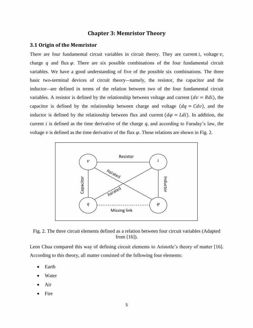
There are four fundamental circuit variables in circuit theory. They are current , voltage ,
charge and flux . There are six possible combinations of the four fundamental circuit
variables. We have a good understanding of five of the possible six combinations. The three
basic two-terminal devices of circuit theory—namely, the resistor, the capacitor and the
inductor—are defined in terms of the relation between two of the four fundamental circuit
variables. A resistor is defined by the relationship between voltage and current , the
capacitor is defined by the relationship between charge and voltage and the
inductor is defined by the relationship between flux and current . In addition, the
current is defined as the time derivative of the charge and according to Faraday‘s law, the
voltage is defined as the time derivative of the flux . These relations are shown in Fig. 2.
Fig. 2. The three circuit elements defined as a relation between four circuit variables (Adapted
from [16]).
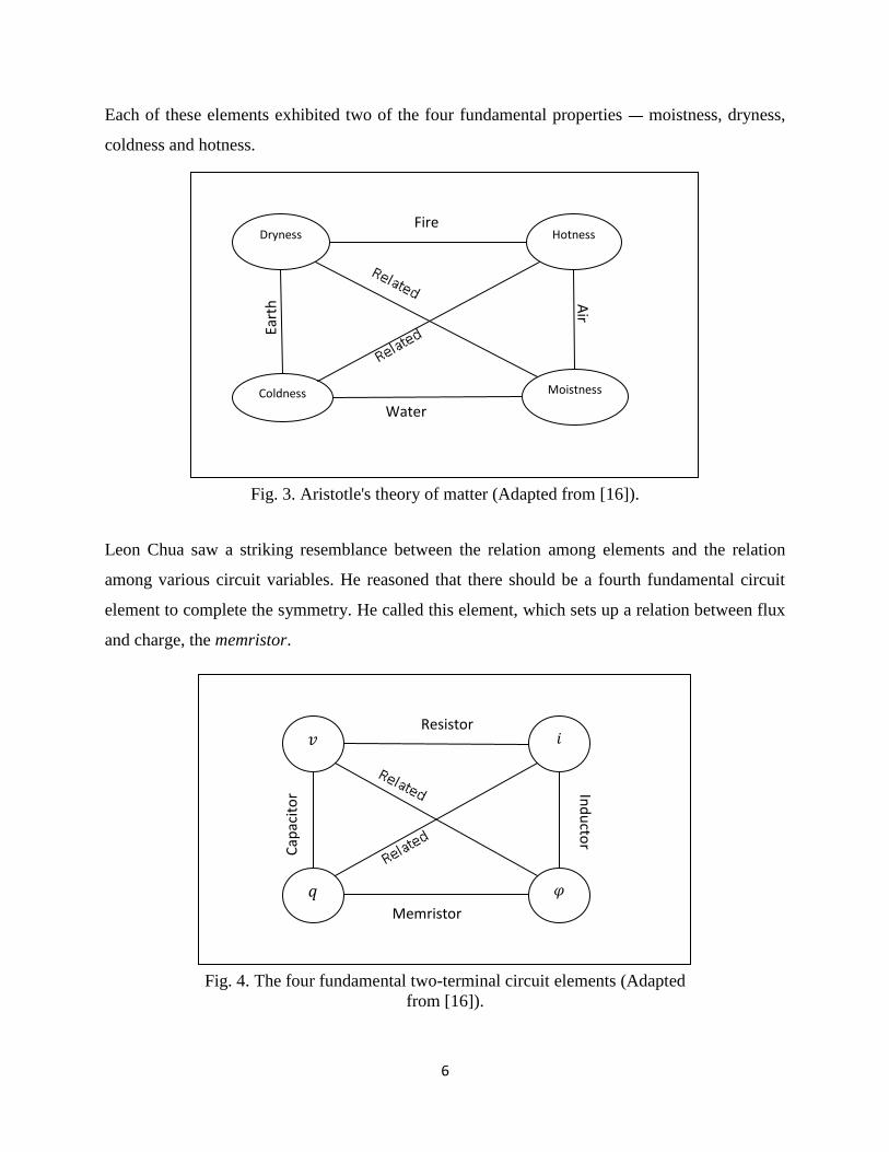
Leon Chua compared this way of defining circuit elements to Aristotle‘s theory of matter [16].
According to this theory, all matter consisted of the following four elements:
Earth
Water
Air
Fire
Resistor
Ind
ucto
r Cap
acit
or
Missing link
6
Each of these elements exhibited two of the four fundamental properties — moistness, dryness,
coldness and hotness.
Leon Chua saw a striking resemblance between the relation among elements and the relation
among various circuit variables. He reasoned that there should be a fourth fundamental circuit
element to complete the symmetry. He called this element, which sets up a relation between flux
and charge, the memristor.
Resistor
Ind
ucto
r Cap
acit
or
Memristor
Dryness
Coldness Moistness
Hotness Fire
Air
Eart
h
Water
Fig. 3. Aristotle's theory of matter (Adapted from [16]).
Fig. 4. The four fundamental two-terminal circuit elements (Adapted
from [16]).
7
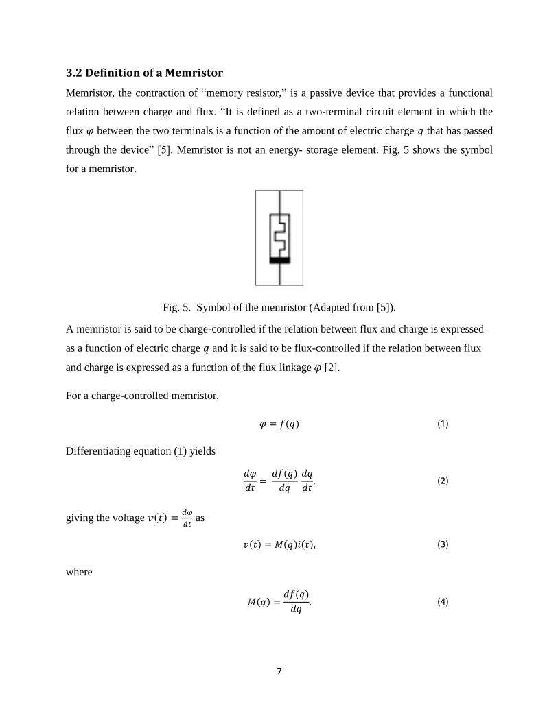
3.2 Definition of a Memristor
Memristor, the contraction of ―memory resistor,‖ is a passive device that provides a functional
relation between charge and flux. ―It is defined as a two-terminal circuit element in which the
flux between the two terminals is a function of the amount of electric charge that has passed
through the device‖ [5]. Memristor is not an energy- storage element. Fig. 5 shows the symbol
for a memristor.
Fig. 5. Symbol of the memristor (Adapted from [5]).
A memristor is said to be charge-controlled if the relation between flux and charge is expressed
as a function of electric charge and it is said to be flux-controlled if the relation between flux
and charge is expressed as a function of the flux linkage [2].
For a charge-controlled memristor,
(1)
Differentiating equation (1) yields
(2)
giving the voltage
as
(3)
where
(4)

8
is called as memristance, and it has the units of resistance. Memristance defines a linear
relationship between current and voltage, as long as the charge does not vary. Thus if is
constant, a memristor behaves as a resistor.
For a flux-controlled memristor,
(5)
Differentiating equation (5) yields
(6)
giving the current
as
(7)
where
(8)
is called as memductance and it has the units of conductance.
3.3 What is Memristance?
Memristance is a property of the memristor [17]. When the charge flows in one direction through
a circuit, the resistance of the memristor increases, and its resistance decreases when the charge
flows in the opposite direction in the circuit. If the applied voltage is turned off, thus stopping the
flow of charge, the memristor ―remembers‖ the last resistance that it had. When the flow of
charge is started again, the resistance of the circuit will be what it was when it was last active.
3.4 Analogy of a Memristor
An analogy of a memristor is described in [17]. A resistor is analogous to a pipe through which
water flows. The pressure of water at the input of the pipe is analogous to the voltage, and water
is analogous to electric charge. The rate of flow of water through the pipe is similar to electric
current. If the pipe has a larger diameter, the flow of water through the pipe is faster, just like
more current flows through resistor with a small value of resistance. An analogy for a memristor
is a different kind of pipe—whose diameter expands or shrinks depending on the direction of the

9
water flow through it. The diameter of the pipe increases when the water flows in one direction,
enabling water to flow faster, and the diameter of the pipe decreases when the water flows in the
opposite direction, thus slowing down the water flow. If no water is let into the pipe, the pipe
will retain its most recent diameter until the water is turned back on. Thus, the pipe remembers
the amount of the water that has flowed through it.
3.5 Properties of a Memristor
3.5.1 – Curve of a Memristor
The – curve of a memristor is a monotonically increasing [16]. The memristance is the
slope of the – curve. According to the memristor passivity condition, a memristor is passive if
and only if memristance is non-negative [2]. If M(q) ≥ 0, then the instantaneous power
dissipated by the memristor, is always positive, and so the memristor is a
passive device [9]. The memristor is purely dissipative, like a resistor. Thus, the – curve of a
memristor is always a monotonically increasing function. Fig. 6 shows some examples of typical
– curves of memristors.
Fig. 6. Typical – curves of memristors(Adapted from [16]).
3.5.2 Current–Voltage Curve of a Memristor
An important fingerprint of a memristor is the ―pinched hysteresis loop‖ current—voltage
characteristic [16]. For a memristor excited by a periodic signal, when the voltage is zero,
the current is also zero and vice versa. Thus, both voltage and current have

10
identical zero-crossing. If any device has a current–voltage hysteresis curve, then it is either a
memristor or a memristive device [16]. Another signature of the memristor is that the ―pinched
hysteresis loop‖ shrinks with the increase in the excitation frequency [16]. Figure 7 shows the
―pinched hysteresis loop‖ and an example of the loop shrinking with the increase in frequency.
In fact, when the excitation frequency increases towards infinity, the memristor behaves as a
normal resistor.
3.6 Memristive Systems
In 1976, five years after Chua‘s paper on the memristor, he and Kang [3] published a paper
defining a much broader class of systems, named memristive systems. The memristive systems
are described by
(9)
Fig. 7. The pinched hysteresis loop and the loop shrinking with the increase in frequency
(Adapted from [18]).
11
and
(10)
where is a set of state variables, and can be functions of time, and and are the voltage
and current, respectively.
The fundamental memristive system theorem states that ―every two-terminal device which
exhibits a pinched hysteresis loop in the current-versus-voltage plane when driven by a dc and/or
sinusoidal signal of any frequency is a memristive system‖[16].

12
Chapter 4: Model of the Memristor from HP Labs
In 2008, thirty-seven years after Chua proposed the memristor, Stanley Williams and his group at
HP Labs realized the memristor in device form. The HP model of the memristor is described in
[9]. To realize a memristor, they used a very thin film of titanium dioxide (TiO2). The thin film is
sandwiched between two platinum (Pt) contacts and one side of TiO2 is doped with oxygen
vacancies. The oxygen vacancies are positively charged ions. Thus, there is a TiO2 junction
where one side is doped and the other side is undoped. The device established by HP is shown in
Fig. 8.
In Fig.8, D is the device length and w is the length of the doped region. Pure TiO2 is a
semiconductor and has high resistivity. The doped oxygen vacancies make the TiO2-x material
conductive. The working of the memristor established by HP is described in [19]. When a
positive voltage is applied, the positively charged oxygen vacancies in the TiO2-x layer are
repelled, moving them towards the undoped TiO2 layer. As a result, the boundary between the
two materials moves, causing an increase in the percentage of the conducting TiO2-x layer. This
increases the conductivity of the whole device. When a negative voltage is applied, the positively
charged oxygen vacancies are attracted, pulling them out of TiO2 layer. This increases the
amount of insulating TiO2, thus increasing the resistivity of the whole device. When the voltage
is turned off, the oxygen vacancies do not move. The boundary between the two titanium dioxide
Fig. 8. Schematic of HP memristor (Adapted from [9]).

13
layers is frozen. This is how the memristor ‗remembers‘ the voltage last applied. Figure 9
explains the behavior of the memristor model when positive and negative voltage is applied. Fig.
9(a) shows the thin film of titanium-dioxide where one side is doped with positive oxygen
vacancies and the other side is the undoped. Fig. 9(b) shows the behavior when a positive voltage
is applied. The positive oxygen vacancies are repelled and they move towards the undoped TiO2
layer, reducing the percentage of the insulating TiO2, thus decreasing the resistivity. Fig. 9(c)
shows the behavior when a negative voltage is applied. The positive oxygen vacancies are
attracted and they move towards the doped TiO2-x layer, increasing the percentage of the
insulating TiO2, thus increasing the resistivity.
Fig. 9. Behavior of HP memristor when positive and negative voltages are applied (Adapted
from [20]).

14
The simple mathematical model [9], [10] of the HP memristor is given by
(11)
where
has the dimensions of magnetic flux. is the average drift velocity and has the
units cm2/sV; is the thickness of titanium-dioxide film; and are ‗on-state‘ and ‗off-
state‘ resistances; and is the total charge passing through the memristor device.
4.1 Linear Drift Model [9]
Let us assume a uniform electric field across the device. Therefore, there is a linear relationship
between drift-diffusion velocity and the net electric field. The state equation can be written as
(12)
Integrating (12) gives
(13)
where is the initial length of . The speed of drift under a uniform electric field across the
device is then given by
(14)
In an uniform field In this case, defines the amount of charge required to
move the boundary from where , to distance , where . Therefore,
. Thus,
(15)
If
, then equation 15 can be written as
(13)

15
(16)
The amount of charge that is passed through the channel over the required charge for a
conductive channel is given as
. Using the equations in [10] , we have
(17)
Substituting
in Eq. 17, we get
(18)
If we assume that the initial charge then , and
(19)
where
and is the memristance value at . Thus the memristance at time is given
by
(20)
where . When , .
Substituting equation 20 into , when
we get,
(21)
Since
, the solution is
(22)
For , Eq. 22 becomes
16
(23)
If
, then the internal state of the memristor is
(24)
The current-voltage relationship in this case is
(25)
Eq. 25 shows the inverse-square relation between memristance and TiO2 thickness, . Thus, for
smaller values of , the memristance shows improved characteristics. Nowadays, memristance
becomes more important for understanding as the dimensions of electronic devices are shrinking
to nanometer scale.

17
Chapter 5: Results and Simulations
5.1 SPICE Model [21]
Biolek, et al., provided in [21] a useful SPICE model of a memristor, the structure of which is
shown in Fig. 10.
In the above circuit, is the input voltage and is modeled to be the current through the
memristor. The flux is calculated by integrating the voltage and the charge is calculated by
integrating the current is the voltage source whose terminal voltage is controlled
according to the formula ― is a current source whose current is controlled according
to the equation ― where is the voltage across the capacitor and it models
the normalized width of the doped layer.
The relation between memristor current and voltage is modeled as on the basis of Eq. 26
(26)
+
-
+
- +
-
+
_
Fig. 10. Structure of the SPICE model (Adapted from [6]).

18
where
(27)
is the resistor in series voltage source whose terminal voltage is controlled by the formula,
. The voltage across the capacitor models the normalized width of the doped
layer. The initial state of is modeled by the initial voltage of the capacitor. The flux is
calculated by the time-integral of voltage, and the charge is calculated by the time-integral of
current. The listing for the SPICE model is included in the appendix.
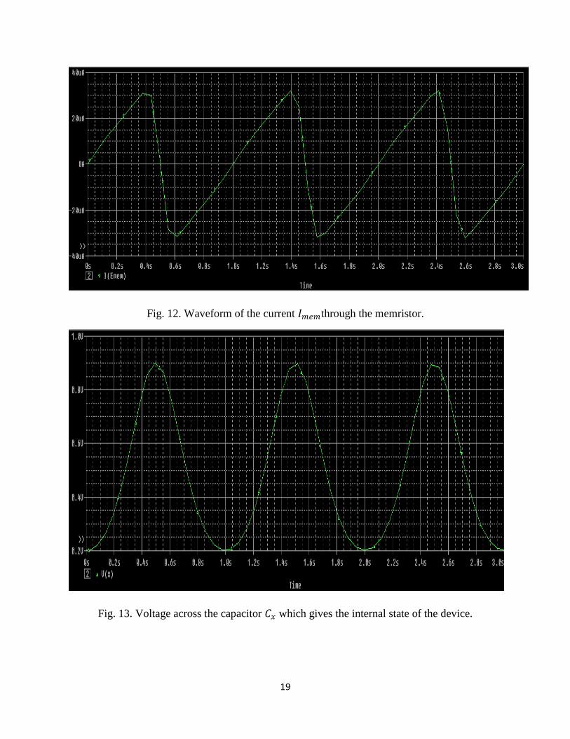
5.2 Simulation Results— Using SPICE model
5.2.1 Simulations for a Memristor Driven by Voltage using PSPICE
For this simulation, the width of the TiO2 film is considered to be 10 nm and the dopant
mobility = 10-10
cm2
s-1
V-1
. The values assumed are- =1KΩ, =100KΩ and the initial
resistance required to model the initial conditions of the capacitor is assumed to be 80KΩ.
The simulation results are shown below in Figs. 11, 12, 13, 14, 15, 16 and 17.
Fig. 11. An input voltage applied to the memristor.
19
Fig. 12. Waveform of the current through the memristor.
Fig. 13. Voltage across the capacitor which gives the internal state of the device.
20
Fig. 14. Charge-versus-flux curve for memristor.
Fig. 15. Current-versus-voltage curve for input frequency of 1 Hz.
21
Fig. 16. Current-versus-voltage curve for input frequency of 1.5 Hz.
Fig. 17.Current-versus-voltage curve for input frequency of 2 Hz.
From Fig. 14, we can see that the flux—charge curve is a monotonically increasing curve. We
can also observe the current—voltage ―pinched hysteresis loop‖ and the hysteresis loop shrinking

22
with the increase in the input frequency in Fig. 15, Fig. 16 and Fig. 17. Thus, all the properties
that are said to be a signature of a memristor are satisfied.
5.3 Simulation Results— Using MATLAB
5.3.1 Simulations for a Memristor Driven by Voltage using MATLAB
Using the equations (23), (24) and (25), studied in Chapter 4, a memristor is simulated using
MATLAB. For this simulation, the width of the TiO2 film is considered to be 10 nm and the
dopant mobility = 10-10
cm2
s-1 V
-1. The values assumed are — =100Ω , =16KΩ. The
simulation results are shown below. The MATLAB code is included in the appendix.
Fig. 18. Plot of flux versus charge.
0 0.1 0.2 0.3 0.4 0.5 0.6 0.70
1
2
3
4
5
6x 10
-5
flux
charg
e
Plot of charge versus flux

23
Fig. 19. Plot of current versus voltage for ω = 3 rad/s.
Fig. 20. Plot of current versus voltage for ω = 8 rad/s.
-1 -0.8 -0.6 -0.4 -0.2 0 0.2 0.4 0.6 0.8 1-1
-0.8
-0.6
-0.4
-0.2
0
0.2
0.4
0.6
0.8
1x 10
-4
voltage
curr
ent
Plot of current versus voltage
-1 -0.8 -0.6 -0.4 -0.2 0 0.2 0.4 0.6 0.8 1-8
-6
-4
-2
0
2
4
6
8x 10
-5
voltage
curr
ent
Plot of current versus voltage
24
From Fig. 18, we can see that the flux–charge curve is a monotonically increasing curve. Fig. 19
and Fig. 20 show the current–voltage ―pinched hysteresis loop‖ and the hysteresis loop is
shrinking with the increase in the input frequency. Thus, all the properties that are said to be a
signature of a memristor are satisfied.

25
Chapter 6: Potential Applications of Memristor
6.1 Two-state Charge-controlled Memristor [16]
The φ–q curve of a two-state charge-controlled memristor is shown in Fig. 21. The slope of the
φ–q curve gives the memristance . The two values of the memristance can be considered as
two different states which can be used as binary states. The memristor holds logical values as
impedance state and not as voltages. The resistance can be changed from one state to another by
applying appropriate voltage.
Fig. 21. – curve of a two-state charge-controlled memristor
6.2 Digital Logic Implementation Using Memristor
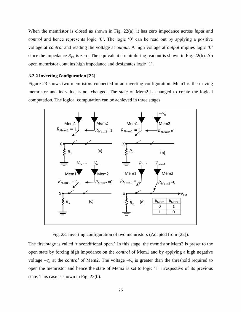
6.2.1 Memristor as a Logical State Element [22]
Consider the memristor shown in Fig. 22. One of the terminals of the memristor is connected to
control and the other is connected to either input or output.
Fig. 22. Memristor as a state element (Adapted from [22]).
CONTROL CONTROL
Input Output Output
(a) (b)
26
When the memristor is closed as shown in Fig. 22(a), it has zero impedance across input and
control and hence represents logic ‘0‘. The logic ‗0‘ can be read out by applying a positive
voltage at control and reading the voltage at output. A high voltage at output implies logic ‘0‘
since the impedance is zero. The equivalent circuit during readout is shown in Fig. 22(b). An
open memristor contains high impedance and designates logic ‗1‘.
6.2.2 Inverting Configuration [22]
Figure 23 shows two memristors connected in an inverting configuration. Mem1 is the driving
memristor and its value is not changed. The state of Mem2 is changed to create the logical
computation. The logical computation can be achieved in three stages.
Fig. 23. Inverting configuration of two memristors (Adapted from [22]).
The first stage is called ‗unconditional open.‘ In this stage, the memristor Mem2 is preset to the
open state by forcing high impedance on the control of Mem1 and by applying a high negative
voltage – at the control of Mem2. The voltage – is greater than the threshold required to
open the memristor and hence the state of Mem2 is set to logic ‗1‘ irrespective of its previous
state. This case is shown in Fig. 23(b).
Mem1 Mem2 Mem1 Mem2
Mem1 Mem2 Mem1 Mem2
X
X
X
X
=1
=1
=0
=0
RMem1 RMem2
0 1
1 0
Vout
(a) (b)
(d) (c)

27
The second stage is called the ‗conditional close‘ and this stage is shown in Fig. 23(c). The
memristor Mem1 is placed in the read out mode by applying a voltage at its control
terminal. A voltage is applied at the control of Mem2. If memristor Mem1 is closed, the
impedance =0. This makes the voltage at the intermediate node X close to . The
voltage across Mem2 is ( - ) which is not enough to close Mem2 and it remains in the
open state. If Mem1 is open, the voltage on node X is close to zero and the voltage across Mem2
is . The voltage drop is over the threshold of Mem2 and it closes memristor Mem2. Thus,
logical operation of inversion takes place. The truth table is shown in Fig. 23.
The third stage is ‗read out.‘ The control node of Mem1 is placed in high impedance so that it
does not have an effect to node X. A voltage is applied at the control terminal of Mem2.
This will result a voltage at output, depending on the state of Mem2.
6.2.3 NAND Operation [22]
Consider the set of memristors as shown in Fig.24. The memristor Mem1 of inverting
configuration is replaced by set of memristors Mem1-Mem3, which are connected in parallel.
The control terminals of Mem1-Mem3 are connected. The memristor Mem4 is unconditionally
open by applying a high negative voltage – at the control terminal. Then a voltage is
applied at the common control terminal and is applied to the control of Mem4. In the
scenario where memristors Mem1-Mem3 are open, the voltage at the terminal X is close to 0.
The voltage drop across Mem4 is , which is enough to close Mem4. In the scenario where one
memristor Mem1 is closed and Mem2 and Mem3 are open, the intermediate node settles close to
and the voltage across Mem4 is not enough to close the memristor. Similar results occur
when Mem2 or Mem3 are open. Hence, the logical computation can be treated as Mem4 =
(Mem1.Mem2.Mem3)` which is NAND operation. This configuration is referred to as ‗wired-
AND‘ as various inputs are wired together to produce result.
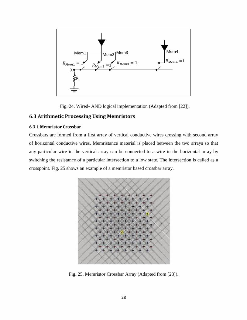
28
Fig. 24. Wired- AND logical implementation (Adapted from [22]).
6.3 Arithmetic Processing Using Memristors
6.3.1 Memristor Crossbar
Crossbars are formed from a first array of vertical conductive wires crossing with second array
of horizontal conductive wires. Memristance material is placed between the two arrays so that
any particular wire in the vertical array can be connected to a wire in the horizontal array by
switching the resistance of a particular intersection to a low state. The intersection is called as a
crosspoint. Fig. 25 shows an example of a memristor based crossbar array.
Fig. 25. Memristor Crossbar Array (Adapted from [23]).
X
Rx
1 1
1
Mem1 Mem2 Mem3 Mem4

29
6.3.2 Arithmetic Processing [24]
The memristor crossbar array can be used for arithmetic processing. Fig. 26 shows example of a
memristor crossbar array which includes a horizontal wire intersected by eight vertical wires and
the memristor is sandwiched between the horizontal wire and the vertical wires. An input voltage
below the threshold, required for changing the resistance of the memristor is applied to the
vertical wires. Assuming that the memristor may be approximated as a fuse (i.e. high resistance
is approximately an open circuit and low resistance is a short circuit), the output current in the
horizontal wire can be calculated based on the ratio of the input voltage and the parallel
combination of the number of low resistances. Thus if one low resistance state produces a current
of I, two low resistance states will produce a current of 2I, three low resistance states will
produce a current of 3I and so on.
Fig. 26. Memristor crossbar array which includes a horizontal wire intersected by eight vertical
wires (Adapted from [24]).
In the system illustrated in Fig. 27 each column of the crossbar is configured to store the
equivalent of a binary numerical value where low resistance states are indicated as a closed
connection and high resistance states are open connections. Each row wire includes a weighting
resistor set to be sufficiently larger than the low-resistance state of the memristor so that each
I
I
2I
3I
30
row has an associated bit significance ranging from a least significant bit row (uppermost row) to
a most significant bit row (lowermost row). By selecting particular columns (i.e. applying a
positive voltage less than the threshold necessary to alter the resistance of the memristor
material) the binary numerical values of these columns may be added together. In the example of
Fig. 27, the second, third, and sixth column values are summed. In the second column, only the
second-row crosspoint is in a low-resistance state, so this contributes a current of approximately
(
). In the third column, the first and second row crosspoints are in the low-resistance
states which contribute ( +
= ) to the current. In the sixth column,
the second and third row crosspoints are in the low-resistance states, which contribute (
+
= ) to the current. The overall current is thus (
+
+ = ). Using an analog-to-digital converter with a resolution set to
, the output is converted to 1011, which is the expected sum (0010 + 0011 + 0110).
Fig. 27. Memristor crossbar array as an arithmetic processor (Adapted from [24]).
The above configuration has some disadvantages, one being that the analog circuitry can be more
sensitive to noise than purely digital electronics, but it has the advantage of integrating memory
with computation. Thus, the use of memristors enables calculation on the same chip where the
data is stored.
ADC 11I
0 1 1 0 0 1 0 0
1011
31
6.4 Memristor Memory
Memristors can be used as non-volatile memory, allowing greater data density than hard drives
[5]. The memristor based crossbar latch memory prototyped by HP can fit 100 gigabits within a
square centimeter [5]. HP also claims that memristor memory can handle up to 1,000,000
read/write cycles before degradation, compared to flash at 100,000 cycles [25]. In addition,
memristors also consume less power.
In memristor memories, the reading operation is performed by applying a voltage lesser than the
threshold value. The memristor will conduct even at this voltage if it is ‗on‘. If it is ‗off‘ then it
will not conduct. To write one of the logic levels (0 or 1) a voltage greater than the threshold
value is applied. To write the other logic level, a voltage of opposite polarity whose magnitude is
greater than the threshold voltage is applied. This turns the memristor ‗off‘.
Memristors can ‗remember‘ even when the power is turned off. Thus, the computers developed
using memristors will have no boot up time [16]. The computer can be turned on, like turning on
a light switch and it will instantly display all information that was there on it when it was turned
off [26].

32
Chapter 7: Conclusion and Future Research
7.1 Conclusion
This report presents a detailed study of the memristor. The properties of the memristor and the
model proposed by HP are discussed. This model is simulated by subjecting it to various input
voltages and noting the results obtained. This report also presents a brief insight into the potential
applications of the memristor.
Nanotechnology is fast emerging, and nanoscale devices automatically bring in memristive
functions. Thus, memristors might revolutionize the 21st century as radically as the transistor in
the 20th
century. Memristor memories have already been developed and the researchers at HP
believe that they can offer a product with a storage density of about 20 gigabytes per square
centimeter by 2013.
Leon Chua rightly said ―It‘s time to rewrite all the Electronics Engineering books.‖ [16]
7.2 Future Research
Recently, researchers have defined two new memdevices- memcapacitor and meminductor, thus
generalizing the concept of memory devices to capacitors and inductors. These devices also
show ‗pinched‘ hysteresis loops in two constitutive variables— charge—voltage for the
memcapacitor and current—flux for meminductor. Figure 28 shows the symbols for the
memcapacitor and the meminductor.
Fig. 28. Symbol of memcapacitor and meminductor (Adapted from [27]).

33
Memristors are not lossless devices. As non-volatile memories, memristors do not consume
power when idle but they do dissipate energy when they are being read or written. Hence, there
is a need to invent lossless non-volatile device. Memcapacitors and meminductors are good
contenders as they are lossless devices.
34
References
[1] James M. Tour and Tao He, ―The fourth element‖,
http://www.aldebaran.cz/bulletin/2009_02/Tour.pdf
[2] Chua, L.O., ―Memristor- the missing circuit element‖, IEEE Trans. Circuit Theory, 1971,
vol. CT-18, no. 5, pp. 507-519.
[3] Chua, L.O. and Kang, S.M.. ―Memristive devices and systems‖, Proceedings of the IEEE,
1976, vol. 64, no. 2, pp. 209-223.
[4] S.Thakoor, A. Moopenn, T. Daud, and A.P. Thakoor, "Solid-state thin-film memistor for
electronic neural networks", Journal of Applied Physics, vol. 67, March 15, 1990, p. 3132-3135
[5] ―Memristor‖- Wikipedia, http://en.wikipedia.org/wiki/Memristor
[6] Buot F.A. and Rajgopal A.K., ―Binary information storage at zero bias in quantum-well
diodes‖, Journal of Applied Physics, November 1994, vol. 76, issue 9, 5552 - 5560
[7] Beck, A., Bednorz, J. G., Gerber, Ch.,Rossel, C., Widmer, D., ―Reproducible switching effect
in thin oxide films for memory applications‖, Applied Physics Letters, No. 1, Jul. 3, 2000, pp.
139-141.
[8] Shangqing Liu, NaiJuan Wu, Xin Chen, and Alex Ignatiev , ―A New Concept for Non-
Volatile Memory — The Electric Pulse Induced Resistive Change Effect in Colossal
Magnetoresistive Thin Films‖, Non-Volatile Memory Technology Symposium, Nov. 7, 2001,
pp. 1-7.
[9] Kavehei, O., Kim, Y.S., Iqbal, A., Eshraghian, K., Al-Sarawi, S.F., Abbott, D.,‖ The Fourth
Element: Characteristics, Modelling, and Electromagnetic Theory of the Memristor‖,
arXiv:1002.3210v1 [cond-mat.mes-hall] (access via http://arxiv.org/abs/1002.3210).
[10] Strukov, D.B., Snider, G.S., Stewart, D.R., Williams, R.S., ―The missing memristor found‖,
Nature, 2008, 1 May 2008, vol. 453, pp. 80-83.
35
[11] Victor Erokhin, Marco P. Fontana, ―Electrochemically controlled polymeric device: a
memristor (and more) found two years ago‖, arXiv:0807.0333v1 [cond-mat.soft] (access via
http://arxiv.org/abs/0807.0333)
[12] J. Joshua Yang, Matthew D. Pickett, Xuema Li, Douglas A. A. Ohlberg, Duncan R.
Stewart & R. Stanley Williams, ―Memristive switching mechanism for metal/oxide/metal nano-
devices‖, Nature Nanotechnology 3, 429 - 433 (2008)
[13] Yuriy V. Pershin, Steven La Fontaine & Massimiliano Di Ventra, ―Memristive model of
amoeba‘s learning,‖ arXiv:0810.4179v3 [q-bio.CB] (access via http://arxiv.org/abs/0810.4179).
[14] Sung Hyun Jo, Kuk-Hwan Kim, and Wei Lu ,―High-Density Crossbar Arrays Based on a Si
Memristive System,‖ NanoLetters ,2009.
[15] Nadine Gergel-Hackett, Behrang Hamadani, Barbara Dunlap, John Suehle, Curt Richter,
Christina Hacker, David Gundlach, ―A Flexible Solution-Processed Memristor‖, IEEE Electron
Device Letters, vol. 30, issue 7, 706-708.
[16] ―Memristor and Memristive Systems Symposium‖,
http://www.youtube.com/watch?v=QFdDPzcZwbs
[17] ―HP Memristor FAQ‖, http://www.hpl.hp.com/news/2008/apr-jun/memristor_faq.html
[18] Wang, F.Y., ―Memristor for introductory physics‖, arXiv:0808.0286 v1 [physics.class-ph]
(access via http://arxiv.org/abs/0808.0286).
[19] Shailendra and Pankaj, ―Memristor: The Missing Link Discovered‖,
http://www.scribd.com/doc/22289654/MEMRISTOR-2
[20] Sreejith A.G, ―Memristor‖, http://www.slideshare.net/jithoot/memristor-3024732
[21] Biolek, Z., Biolek, D., and Biolkova, V., ―SPICE model of memristor with nonlinear dopant
drift‖, Radioengineering J., vol. 18, no. 2, June 2009, pp. 210-214.
36
[22] Tezaswi Raja, Samiha Mourad, ―Digital Logic Implementation in Memristor-Based
Crossbars – A Tutorial‖, Fifth IEEE International Symposium on Electronic Design, Test &
Applications, 2010.
[23] Qiangfei Xia, Warren Robinett, Michael W. Cumbie, Neel Banerjee, Thomas J. Cardinali, J.
Joshua Yang, Wei Wu, Xuema Li, William M. Tong,Dmitri B. Strukov, Gregory S. Snider,
Gilberto Medeiros-Ribeiro, and R. Stanley Williams, ―Memristor- CMOS Hybrid Integrated
Cicuits for Reconfigurable Logic‖, NanoLetters , 2009, 9 (10), pp. 3640–3645.
[24] ]―Programmable Electronics using Memristor Crossbars‖,
http://knol.google.com/k/programmable-electronics-using-memristor-
crossbars#ARITHMETIC_PROCESSING_WITH_MEMRISTORS
[25] ―Unleashing the memristor‖, http://www.hpcwire.com/blogs/Unleashing-the-Memristor-
90992999.html
[26] Jim Walker, ―Memristors and the future‖, http://nobeliefs.com/memristor.htm
[27] Massimiliano Di Ventra, Yuriy V. Pershin, Leon O. Chua, ―Putting memory into circuit
elements: memristors, memcapacitors and meminductors‖,
http://physics.ucsd.edu/~diventra/PointofViewDPC6.pdf
[28] Hoang Manh Thang, ―Memristor model‖
http://www.mathworks.com/matlabcentral/fileexchange/25082
[29] B. Srinivasa Sasidhar., ―Memristor, The New Fundamental Circuit Element‖,
http://www.scribd.com/doc/28916914/MEMRISTOR
[30]‖Memistors, Memristors, and the Rise of Strong Artificial Intelligence‖,
http://knol.google.com/k/memistors-memristors-and-the-rise-of-strong-artificial-intelligence#
[31] David E Burger and Nbrewer, ―Memristor‖, IEEE Global History Network,
http://www.ieeeghn.org/wiki/index.php/Memristor
[32] R. Williams, ―How We Found The Missing Memristor‖, IEEE Spectrum, vol 45, no.12, pp.
28-35, 2008.
37
[33]Yempo Ho., Garng. M. Huang., Peng Li., ―Nonvolatile Memristor Memory: Device
Characteristics and Design Implications‖, ICCAD’09, November 2-5, 2009, San Jose, CA.
[34] Joglekar, Y.N., Wolf, S.J., ―The elusive memristor: properties of basic electrical circuits‖,
European Journal of Physics. 30, pp. 661-675, 2009.

38
Appendix
MATLAB Code for Memristor Simulation
For this simulation, the width of the TiO2 film is considered to be 10 nm and the dopant
mobility = 10-10
cm2
s-1 V
-1. The values assumed are — =100Ω , =16KΩ. The input
frequency considered is 3 rad/s. The equations used for charge, the internal state of the
memristor and current are
and
% MATLAB code for simulating a memristor
v0=1; % amplitude of the input wave
omega=3; % frequency (rad/s)
MD=1e-14;%drift velocity
ROFF=16e+3; % resistance of undoped region
RON=100;% resistance of the doped region
r=ROFF/RON;
D = 10e-9; % Width of Memristor
w0 = 1e-009; % Width of doped region
R0=(RON*(w0/D))+(ROFF*(1-(w0/D)));
q0=(D^2)/(MD*RON);
deltaR=ROFF-RON;
t=0:0.0095:6;
vt=v0*sin(omega*t);%input voltage
flux=v0*(1-cos(omega*t))/omega;%flux
for n=1:632;
i(n)=(vt(n))/(ROFF*sqrt(1-((2*MD*flux(n))/(r*(D^2))))); %Current
charge(n)=(q0*(1-sqrt(1-((2*flux(n))/(q0*ROFF)))));%charge

39
width(n)= 1-sqrt(1-((2*MD*flux(n))/(r*(D^2))));%internal state of memristor
end
figure(1)
plot(flux,charge);%Plot of charge versus flux
figure(2)
plot (vt,i);%plot of current versus voltage
SPICE Listing for Memristor Simulation [21] The SPICE model used for the simulation is shown below.
The SPICE listing is as follows. The input voltage is a 1 Hz sine wave. For this simulation, the
width of the TiO2 film is considered to be 10 nm and the dopant mobility = 10-10
cm2
s-1
V-1
.
The values assumed are =1KΩ, =100KΩ and the initial resistance =80KΩ .
Memristor1.cir-Memory resistor
Vmem positive 0 SIN(0 1.2 1Hz)
Gx 0 x value={I(Em)*10F*1K/10N^2*f(V(x),1)}
Cx x 0 1 IC={(100K-80K)/(100K-1K)}
+
-
+
- +
-
+
_
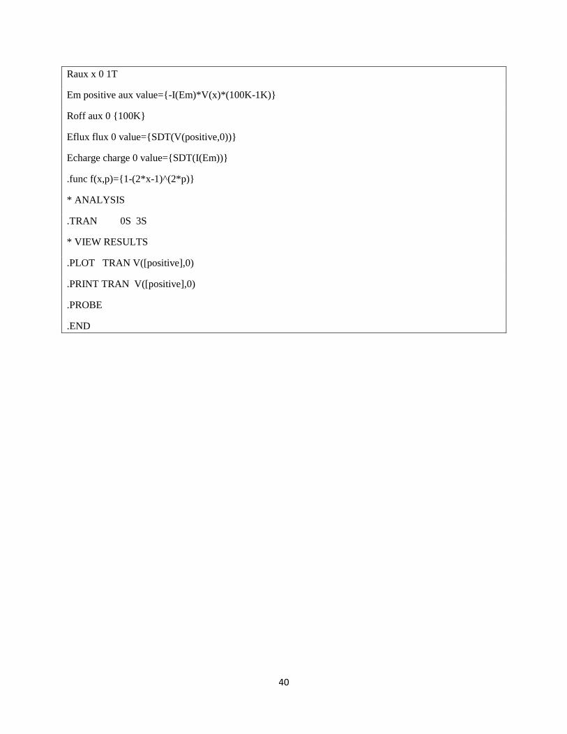
40
Raux x 0 1T
Em positive aux value={-I(Em)*V(x)*(100K-1K)}
Roff aux 0 {100K}
Eflux flux 0 value={SDT(V(positive,0))}
Echarge charge 0 value={SDT(I(Em))}
.func f(x,p)={1-(2*x-1)^(2*p)}
* ANALYSIS
.TRAN 0S 3S
* VIEW RESULTS
.PLOT TRAN V([positive],0)
.PRINT TRAN V([positive],0)
.PROBE
.END