a (s)tem and atom probe tomography study of ingan
TRANSCRIPT

Journal of Physics Conference Series
OPEN ACCESS
A (S)TEM and atom probe tomography study ofInGaNTo cite this article Thorsten Mehrtens et al 2011 J Phys Conf Ser 326 012029
View the article online for updates and enhancements
Related contentMeasuring composition in InGaN fromHAADF-STEM images and studying thetemperature dependence of Z-contrastT Mehrtens M Schowalter D Tytko et al
-
Investigation of optical and concentrationprofile changes of InGaNAsGaAsheterostructures induced by thermalannealingRobert Imlau Knut Muumlller Oleg Rubel etal
-
2D-composition mapping in InGaN withoutelectron beam induced clustering of indiumby STEM HAADF Z-contrast imagingAndreas Rosenauer Thorsten MehrtensKnut Muumlller et al
-
Recent citationsNanoprecipitates in single-crystalmolybdenum-alloy nanopillars detected byTEM and atom probe tomographyEmad Oveisi et al
-
This content was downloaded from IP address 112118137 on 12102021 at 1004
A (S)TEM and atom probe tomography study of InGaN
Thorsten Mehrtens13
Stephanie Bley1 Marco Schowalter
1 Kathrin Sebald
1
Moritz Seyfried1 Juumlrgen Gutowski
1 Stephan S A Gerstl
2 Pyuck-Pa Choi
2 Dierk
Raabe2 and Andreas Rosenauer
1
1 Institute of Solid State Physics University of Bremen 28359 Bremen Germany 2 Max-Planck-Institut fuumlr Eisenforschung GmbH 40237 Duumlsseldorf Germany
E-mail mehrtensifpuni-bremende
Abstract In this work we show how the indium concentration in high indium content
InxGa1-xN quantum wells as they are commonly used in blue and green light emitting diodes
can be deduced from high-angle annular dark-field scanning transmission electron microscopy
(HAADF-STEM) images This method bases on introducing normalized intensities which can
be compared with multislice simulations to determine the specimen thickness or the indium
concentration The evaluated concentrations are compared with atom probe tomography
measurements It is also demonstrated how the quality of focused ion beam prepared TEM-
lamellas can be improved by an additional etching with low energy ions
1 Introduction
InxGa1-xN is a well suited material for opto-electronic devices such as light emitting diodes and laser
diodes due to its variable bandgap which allows for light emission over the whole visible and part of
the ultraviolet spectral range Despite a high dislocation density leading to non-radiative
recombinations InxGa1-xN based LEDs or laser diodes show a very good lighting efficiency The
reason for this is still under discussion but small fluctuations of the indium concentration [1] or the
layer thickness [2] are assumed to cause bandgap minima which work as traps for carriers and thus
prevent them from moving to the dislocations The precise determination of the indium content in such
structures is still challenging In this contribution we will introduce a method how the indium
concentration can be directly derived from HAADF-STEM images
2 Investigated specimen and optical properties
The investigated specimen was an InGaNGaN test structure consisting of high indium content
InxGa1-xN quantum wells separated by GaN barriers It was grown by metalorganic vapour phase
epitaxy (MOVPE) on a low defect-density GaN substrate Optical properties of the specimen were
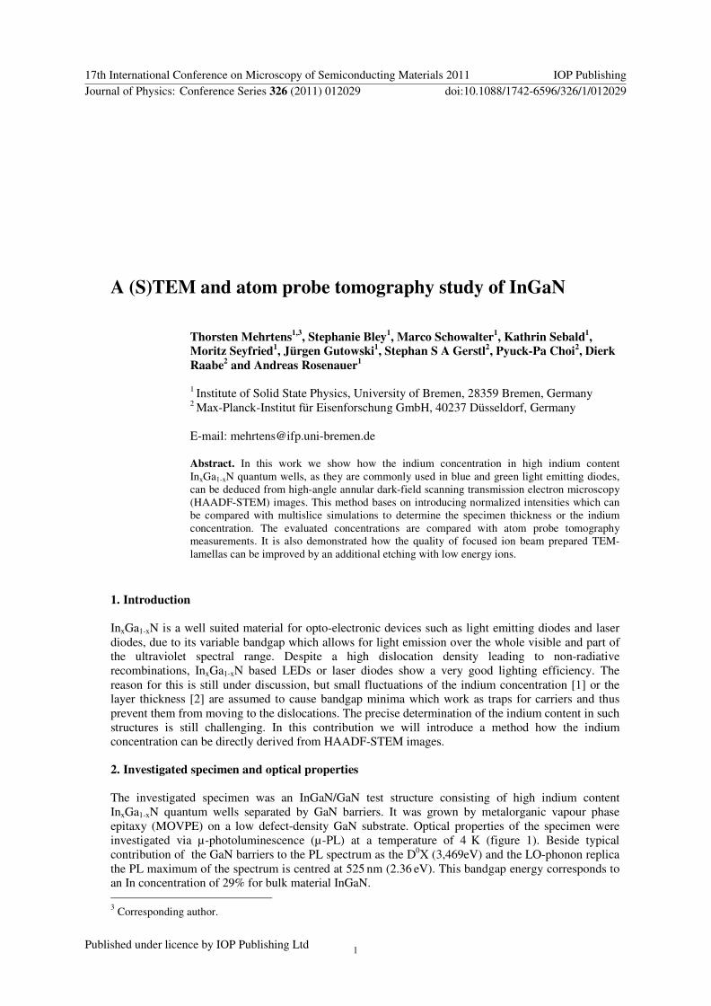
investigated via micro-photoluminescence (micro-PL) at a temperature of 4 K (figure 1) Beside typical
contribution of the GaN barriers to the PL spectrum as the D0X (3469eV) and the LO-phonon replica
the PL maximum of the spectrum is centred at 525 nm (236 eV) This bandgap energy corresponds to
an In concentration of 29 for bulk material InGaN
3 Corresponding author
17th International Conference on Microscopy of Semiconducting Materials 2011 IOP PublishingJournal of Physics Conference Series 326 (2011) 012029 doi1010881742-65963261012029
Published under licence by IOP Publishing Ltd 1
24 28 32 36Energy [eV]
Inte
nsi
ty [
arb
un
its]
500 450 400 350λ [nm]
525 nm
5nm
after FIB after FIB and low-energy ion etching
Figure 1 micro-PL spectrum with maximum at
525nm measured at 4K
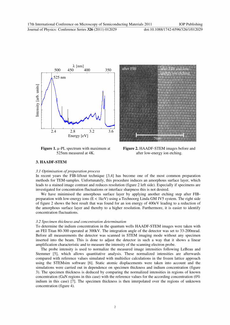
Figure 2 HAADF-STEM images before and
after low-energy ion etching
3 HAADF-STEM
31 Optimisation of preparation process
In recent years the FIB-liftout technique [34] has become one of the most common preparation
methods for TEM-samples Unfortunately this procedure induces an amorphous surface layer which
leads to a stained image contrast and reduces resolution (figure 2 left side) Especially if specimens are
investigated for concentration fluctuations or interface sharpness this is not desired
We have minimised the amorphous surface layer by applying another etching step after FIB-
preparation with low-energy ions (E lt 1keV) using a Technoorg Linda GM IV5 system The right side
of figure 2 shows the best result that was found for an ion energy of 400eV leading to a reduction of
the amorphous surface layer and thereby to a higher resolution Furthermore it is easier to identify
concentration fluctuations
32 Specimen thickness and concentration determination
To determine the indium concentration in the quantum wells HAADF-STEM images were taken with
an FEI Titan 80-300 operated at 300kV The integration angle of the detector was set to 33-200mrad
Before all measurements the detector was scanned in STEM imaging mode without any specimen
inserted into the beam This is done to adjust the detector in such a way that it shows a linear
amplification characteristic and to measure the intensity of the scanning electron probe
The probe intensity is used to normalize the measured image intensities following LeBeau and
Stemmer [5] which allows quantitative analysis These normalized intensities are afterwards
compared with reference values simulated with multislice calculations in the frozen lattice approach
using the STEMsim software [6] Static atomic displacements were taken into account and the
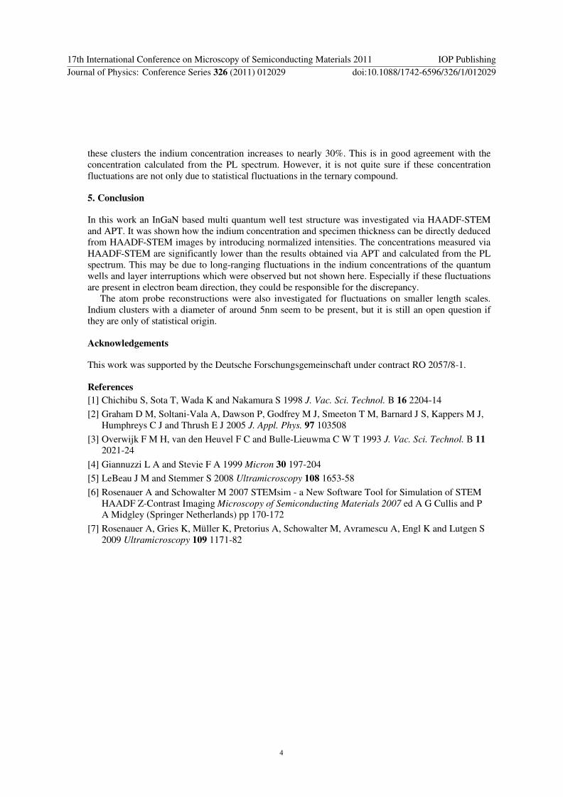
simulations were carried out in dependence on specimen thickness and indium concentration (figure
3) The specimen thickness is deduced by comparing the normalized intensities in regions of known
concentration (GaN regions in this case) with the reference values for the according concentration (0
indium in this case) [7] The specimen thickness is then interpolated over the regions of unknown
concentration (figure 4)
17th International Conference on Microscopy of Semiconducting Materials 2011 IOP PublishingJournal of Physics Conference Series 326 (2011) 012029 doi1010881742-65963261012029
2
Indium concentration []
thic
knes
s [n
m]
0 10 20 30 40 50
180
160
140
120
100
80
60
40
20 01
02
03
04
05
68
72
76
80
y [
nm
]
10
20
x [nm]10 20 30 40
thic
kn
ess
[nm
]
Figure 3 Reference values obtained via
multislice calculations
Figure 4 Specimen thickness derived from GaN
regions and interpolated over the image
To evaluate the indium concentration the normalized intensities in quantum wells are compared with
the reference values this time taking the interpolated thickness of figure 4 into account This leads to
the calculated In concentration map shown in figure 5 The indium content of the two shown layers
increases up to values around 23 Averaged along the monolayers in growth direction ((0002)-
planes) an average concentration of (177plusmn17) for the first (QW1) and (189plusmn18) for the second
quantum well (QW2) can be found for this image but these values fluctuate over the specimen We
observe regions where the quantum wells are interrupted and regions where they possess a lower
concentration
x [nm]
y [
nm
]
10 20 30 40
10
20 0
5
10
15
20
conce
ntr
atio
n [
]
0
5
10
15
20
25
25
con
centr
atio
n [
]
0
5
10
15
20
z [n
m]
0 5 10 15 20 25x [nm]
Figure 5 Indium concentration map
(HAADF-STEM)
Figure 6 Indium concentration map
(Atom probe tomography)
4 Atom probe tomography (APT)
APT measurements were carried out on a laser assisted Imago LEAP 3000 system and the specimen
was reconstructed with the IVAS software The reconstruction was analysed for the average indium
concentration and for small-range indium fluctuations For the average indium concentration all atoms
within bins of 01nm lying in planes perpendicular to the growth direction were taken into account A
maximum indium concentration of around 25 was measured which is significantly higher than the
values obtained from HAADF-STEM Most probable reasons for this deviation are long range
fluctuations of the In concentration that lead to a decrease of the average composition in projection
and the broadening of the electron beam within the specimen
Figure 6 shows a concentration map of one reconstruction averaged over a thickness of 1nm There
seem to be indium clusters with a diameter of around 5nm present especially in the bottom layer In
17th International Conference on Microscopy of Semiconducting Materials 2011 IOP PublishingJournal of Physics Conference Series 326 (2011) 012029 doi1010881742-65963261012029
3
these clusters the indium concentration increases to nearly 30 This is in good agreement with the
concentration calculated from the PL spectrum However it is not quite sure if these concentration
fluctuations are not only due to statistical fluctuations in the ternary compound
5 Conclusion
In this work an InGaN based multi quantum well test structure was investigated via HAADF-STEM
and APT It was shown how the indium concentration and specimen thickness can be directly deduced
from HAADF-STEM images by introducing normalized intensities The concentrations measured via
HAADF-STEM are significantly lower than the results obtained via APT and calculated from the PL
spectrum This may be due to long-ranging fluctuations in the indium concentrations of the quantum
wells and layer interruptions which were observed but not shown here Especially if these fluctuations
are present in electron beam direction they could be responsible for the discrepancy
The atom probe reconstructions were also investigated for fluctuations on smaller length scales
Indium clusters with a diameter of around 5nm seem to be present but it is still an open question if
they are only of statistical origin
Acknowledgements
This work was supported by the Deutsche Forschungsgemeinschaft under contract RO 20578-1
References
[1] Chichibu S Sota T Wada K and Nakamura S 1998 J Vac Sci Technol B 16 2204-14
[2] Graham D M Soltani-Vala A Dawson P Godfrey M J Smeeton T M Barnard J S Kappers M J
Humphreys C J and Thrush E J 2005 J Appl Phys 97 103508
[3] Overwijk F M H van den Heuvel F C and Bulle-Lieuwma C W T 1993 J Vac Sci Technol B 11
2021-24
[4] Giannuzzi L A and Stevie F A 1999 Micron 30 197-204
[5] LeBeau J M and Stemmer S 2008 Ultramicroscopy 108 1653-58
[6] Rosenauer A and Schowalter M 2007 STEMsim - a New Software Tool for Simulation of STEM
HAADF Z-Contrast Imaging Microscopy of Semiconducting Materials 2007 ed A G Cullis and P
A Midgley (Springer Netherlands) pp 170-172
[7] Rosenauer A Gries K Muumlller K Pretorius A Schowalter M Avramescu A Engl K and Lutgen S
2009 Ultramicroscopy 109 1171-82
17th International Conference on Microscopy of Semiconducting Materials 2011 IOP PublishingJournal of Physics Conference Series 326 (2011) 012029 doi1010881742-65963261012029
4
A (S)TEM and atom probe tomography study of InGaN
Thorsten Mehrtens13
Stephanie Bley1 Marco Schowalter
1 Kathrin Sebald
1
Moritz Seyfried1 Juumlrgen Gutowski
1 Stephan S A Gerstl
2 Pyuck-Pa Choi
2 Dierk
Raabe2 and Andreas Rosenauer
1
1 Institute of Solid State Physics University of Bremen 28359 Bremen Germany 2 Max-Planck-Institut fuumlr Eisenforschung GmbH 40237 Duumlsseldorf Germany
E-mail mehrtensifpuni-bremende
Abstract In this work we show how the indium concentration in high indium content
InxGa1-xN quantum wells as they are commonly used in blue and green light emitting diodes
can be deduced from high-angle annular dark-field scanning transmission electron microscopy
(HAADF-STEM) images This method bases on introducing normalized intensities which can
be compared with multislice simulations to determine the specimen thickness or the indium
concentration The evaluated concentrations are compared with atom probe tomography
measurements It is also demonstrated how the quality of focused ion beam prepared TEM-
lamellas can be improved by an additional etching with low energy ions
1 Introduction
InxGa1-xN is a well suited material for opto-electronic devices such as light emitting diodes and laser
diodes due to its variable bandgap which allows for light emission over the whole visible and part of
the ultraviolet spectral range Despite a high dislocation density leading to non-radiative
recombinations InxGa1-xN based LEDs or laser diodes show a very good lighting efficiency The
reason for this is still under discussion but small fluctuations of the indium concentration [1] or the
layer thickness [2] are assumed to cause bandgap minima which work as traps for carriers and thus
prevent them from moving to the dislocations The precise determination of the indium content in such
structures is still challenging In this contribution we will introduce a method how the indium
concentration can be directly derived from HAADF-STEM images
2 Investigated specimen and optical properties
The investigated specimen was an InGaNGaN test structure consisting of high indium content
InxGa1-xN quantum wells separated by GaN barriers It was grown by metalorganic vapour phase
epitaxy (MOVPE) on a low defect-density GaN substrate Optical properties of the specimen were
investigated via micro-photoluminescence (micro-PL) at a temperature of 4 K (figure 1) Beside typical
contribution of the GaN barriers to the PL spectrum as the D0X (3469eV) and the LO-phonon replica
the PL maximum of the spectrum is centred at 525 nm (236 eV) This bandgap energy corresponds to
an In concentration of 29 for bulk material InGaN
3 Corresponding author
17th International Conference on Microscopy of Semiconducting Materials 2011 IOP PublishingJournal of Physics Conference Series 326 (2011) 012029 doi1010881742-65963261012029
Published under licence by IOP Publishing Ltd 1
24 28 32 36Energy [eV]
Inte
nsi
ty [
arb
un
its]
500 450 400 350λ [nm]
525 nm
5nm
after FIB after FIB and low-energy ion etching
Figure 1 micro-PL spectrum with maximum at
525nm measured at 4K
Figure 2 HAADF-STEM images before and
after low-energy ion etching
3 HAADF-STEM
31 Optimisation of preparation process
In recent years the FIB-liftout technique [34] has become one of the most common preparation
methods for TEM-samples Unfortunately this procedure induces an amorphous surface layer which
leads to a stained image contrast and reduces resolution (figure 2 left side) Especially if specimens are
investigated for concentration fluctuations or interface sharpness this is not desired
We have minimised the amorphous surface layer by applying another etching step after FIB-
preparation with low-energy ions (E lt 1keV) using a Technoorg Linda GM IV5 system The right side
of figure 2 shows the best result that was found for an ion energy of 400eV leading to a reduction of
the amorphous surface layer and thereby to a higher resolution Furthermore it is easier to identify
concentration fluctuations
32 Specimen thickness and concentration determination
To determine the indium concentration in the quantum wells HAADF-STEM images were taken with
an FEI Titan 80-300 operated at 300kV The integration angle of the detector was set to 33-200mrad
Before all measurements the detector was scanned in STEM imaging mode without any specimen
inserted into the beam This is done to adjust the detector in such a way that it shows a linear
amplification characteristic and to measure the intensity of the scanning electron probe
The probe intensity is used to normalize the measured image intensities following LeBeau and
Stemmer [5] which allows quantitative analysis These normalized intensities are afterwards
compared with reference values simulated with multislice calculations in the frozen lattice approach
using the STEMsim software [6] Static atomic displacements were taken into account and the
simulations were carried out in dependence on specimen thickness and indium concentration (figure
3) The specimen thickness is deduced by comparing the normalized intensities in regions of known
concentration (GaN regions in this case) with the reference values for the according concentration (0
indium in this case) [7] The specimen thickness is then interpolated over the regions of unknown
concentration (figure 4)
17th International Conference on Microscopy of Semiconducting Materials 2011 IOP PublishingJournal of Physics Conference Series 326 (2011) 012029 doi1010881742-65963261012029
2
Indium concentration []
thic
knes
s [n
m]
0 10 20 30 40 50
180
160
140
120
100
80
60
40
20 01
02
03
04
05
68
72
76
80
y [
nm
]
10
20
x [nm]10 20 30 40
thic
kn
ess
[nm
]
Figure 3 Reference values obtained via
multislice calculations
Figure 4 Specimen thickness derived from GaN
regions and interpolated over the image
To evaluate the indium concentration the normalized intensities in quantum wells are compared with
the reference values this time taking the interpolated thickness of figure 4 into account This leads to
the calculated In concentration map shown in figure 5 The indium content of the two shown layers
increases up to values around 23 Averaged along the monolayers in growth direction ((0002)-
planes) an average concentration of (177plusmn17) for the first (QW1) and (189plusmn18) for the second
quantum well (QW2) can be found for this image but these values fluctuate over the specimen We
observe regions where the quantum wells are interrupted and regions where they possess a lower
concentration
x [nm]
y [
nm
]
10 20 30 40
10
20 0
5
10
15
20
conce
ntr
atio
n [
]
0
5
10
15
20
25
25
con
centr
atio
n [
]
0
5
10
15
20
z [n
m]
0 5 10 15 20 25x [nm]
Figure 5 Indium concentration map
(HAADF-STEM)
Figure 6 Indium concentration map
(Atom probe tomography)
4 Atom probe tomography (APT)
APT measurements were carried out on a laser assisted Imago LEAP 3000 system and the specimen
was reconstructed with the IVAS software The reconstruction was analysed for the average indium
concentration and for small-range indium fluctuations For the average indium concentration all atoms
within bins of 01nm lying in planes perpendicular to the growth direction were taken into account A
maximum indium concentration of around 25 was measured which is significantly higher than the
values obtained from HAADF-STEM Most probable reasons for this deviation are long range
fluctuations of the In concentration that lead to a decrease of the average composition in projection
and the broadening of the electron beam within the specimen
Figure 6 shows a concentration map of one reconstruction averaged over a thickness of 1nm There
seem to be indium clusters with a diameter of around 5nm present especially in the bottom layer In
17th International Conference on Microscopy of Semiconducting Materials 2011 IOP PublishingJournal of Physics Conference Series 326 (2011) 012029 doi1010881742-65963261012029
3
these clusters the indium concentration increases to nearly 30 This is in good agreement with the
concentration calculated from the PL spectrum However it is not quite sure if these concentration
fluctuations are not only due to statistical fluctuations in the ternary compound
5 Conclusion
In this work an InGaN based multi quantum well test structure was investigated via HAADF-STEM
and APT It was shown how the indium concentration and specimen thickness can be directly deduced
from HAADF-STEM images by introducing normalized intensities The concentrations measured via
HAADF-STEM are significantly lower than the results obtained via APT and calculated from the PL
spectrum This may be due to long-ranging fluctuations in the indium concentrations of the quantum
wells and layer interruptions which were observed but not shown here Especially if these fluctuations
are present in electron beam direction they could be responsible for the discrepancy
The atom probe reconstructions were also investigated for fluctuations on smaller length scales
Indium clusters with a diameter of around 5nm seem to be present but it is still an open question if
they are only of statistical origin
Acknowledgements
This work was supported by the Deutsche Forschungsgemeinschaft under contract RO 20578-1
References
[1] Chichibu S Sota T Wada K and Nakamura S 1998 J Vac Sci Technol B 16 2204-14
[2] Graham D M Soltani-Vala A Dawson P Godfrey M J Smeeton T M Barnard J S Kappers M J
Humphreys C J and Thrush E J 2005 J Appl Phys 97 103508
[3] Overwijk F M H van den Heuvel F C and Bulle-Lieuwma C W T 1993 J Vac Sci Technol B 11
2021-24
[4] Giannuzzi L A and Stevie F A 1999 Micron 30 197-204
[5] LeBeau J M and Stemmer S 2008 Ultramicroscopy 108 1653-58
[6] Rosenauer A and Schowalter M 2007 STEMsim - a New Software Tool for Simulation of STEM
HAADF Z-Contrast Imaging Microscopy of Semiconducting Materials 2007 ed A G Cullis and P
A Midgley (Springer Netherlands) pp 170-172
[7] Rosenauer A Gries K Muumlller K Pretorius A Schowalter M Avramescu A Engl K and Lutgen S
2009 Ultramicroscopy 109 1171-82
17th International Conference on Microscopy of Semiconducting Materials 2011 IOP PublishingJournal of Physics Conference Series 326 (2011) 012029 doi1010881742-65963261012029
4