a single-pixel wireless contact lens display · a single-pixel wireless contact lens display a r...
TRANSCRIPT
A single-pixel wireless contact lens display
A R Lingley1, M Ali2, Y Liao1, R Mirjalili1, M Klonner2, M Sopanen2, S Suihkonen2, T Shen3, B P Otis1, H Lipsanen2, and B A Parviz1 1Department of Electrical Engineering, University of Washington, 185 Stevens Way, Seattle, WA 98195-2500 2Department of Micro- and Nanosciences, Aalto University, Tietotie 3, 02150 Espoo, Finland 3Department of Ophthalmology, University of Washington, 325 9th Ave., Seattle, WA 98104 E-mail: [email protected] Abstract:
We present the design, construction, and in vivo rabbit testing of a wirelessly powered contact lens display. The display consists of an antenna, a 500 x 500 µm2 silicon power harvesting and radio integrated circuit, metal interconnects, insulation layers, and a 750 x 750 µm2 transparent sapphire chip containing a micro-light emitting diode with peak emission at 475 nm, all integrated onto a contact lens. The display can be powered wirelessly from 1 m in free space and ~2 cm in vivo on a rabbit. The display was tested on live, anesthetized rabbits with no observed adverse effect. In order to extend display capabilities, design and fabrication of micro-Fresnel lenses on a contact lens are presented to pave the way toward a multi-pixel display that can be worn in the form of a contact lens. Contact lenses with integrated micro-Fresnel lenses were also tested on live rabbits and showed no adverse effect.
1. Introduction
Wearable computing will likely provide new ways to manage information and interact with the world. For example, personal see-through devices could overlay computer-generated visual information on the real world, providing immediate, hands-free access to information [1]. The first step towards always-accessible information and superimposed, data-rich imagery will most likely be implemented in see-through eyeglass displays. Ultimately, a much less cumbersome display for augmented reality may take the form of a contact lens.
In the future, contact lens systems may receive data from external platforms (e.g. mobile phones) and provide real-time notification of important events. As contact lens-based biosensors advance [2], they may alert the wearer of physiological anomalies, such as irregular glucose or lactate levels. With more colors and increased resolution, contact lenses may display text, be used with gaming devices, or offer cues from navigation systems [3]. Our long-term goal is to create a display system that can be comfortably worn in the form of a contact lens, which will include a pixel array, focusing optics, an antenna, and circuitry for power harvesting, radio communication, and pixel control (figure 1).

!"#$%&'()*$+('",$-('(##"./%01.0"'(%#"2$#*'13"
"
4"
"
Figure 1. Conceptual rendition of a multi-pixel contact lens display. (a) A contact lens display comprising a multi-pixel light emitting diode (LED) chip (1), power-harvesting/control circuitry (2), antenna (3), and interconnects (4). These subsystems are encapsulated in a transparent polymer (5), creating a system to project virtual images (6) perceivable by the eye of the wearer. (b) LED chip with 100 pixels. LED active layers can be grown atop a transparent substrate. Emitted light travels through the substrate and is re-imaged using planar Fresnel lenses. (c) Magnified view with one pixel activated, showing Fresnel lenses opposite each LED pixel.
Prior work has shown various types of contact lens functionalization. Contact lens mounted biosensors have been developed to measure eye movement [4,5], tear glucose concentration [6–10], corneal temperature [11], blood oxygen [12], and intraocular pressure [13]. Although it is not contact lens-based, an implanted intraocular vision aid (IOVA) is similar in concept to this project in that it projects images onto the retina from a system of light emitting diodes (LEDs) and microlenses [14].
Integrating displays on contact lenses presents several challenges. First, as the display is stand-alone, power must be provided and stored for system operation without a wired connection. Second, the lens system must be biocompatible and meet regulations for radio frequency (RF) radiation. A third challenge is mechanical and electrical integration of heterogeneous micrometer-scale components (e.g. silicon integrated circuitry and III-V semiconductor optoelectronics) on a polymer substrate. Furthermore, all components must fit within the volume of standard contact lenses, ~1.0 cm2 in area with thicknesses of 200 µm or smaller [15]. Additionally, the human eye, with its relatively long minimum focal distance, cannot resolve objects on a contact lens. We envision two potential solutions to this problem: light from LEDs could be focused using subsidiary lenses, or alternatively, beams from vertical cavity surface emitting lasers could be used to create an image. In this paper, we describe an unfocused single-pixel contact lens display that does not require complex optics.
In the following sections we report how we designed, built, and tested each sub-system of a single-pixel contact lens display. We describe how the sub-systems can be integrated into a fully functional system that can be turned on safely on a live eye. We present our measurement results, including preliminary in vivo rabbit studies, and address our goal of creating a multi-pixel display with fabrication and testing of micro-Fresnel lenses and mutli-pixel LED chips.

!"#$%&'()*$+('",$-('(##"./%01.0"'(%#"2$#*'13"
"
5"
"
2. Design and Fabrication
2.1 System Operation
This single-pixel contact lens display is comprised of a light emitting diode, an antenna, an integrated circuit for power harvesting and LED control, and a polymer substrate with electrical interconnects. An external transmitting antenna emits RF radiation that is collected by the on-lens antenna, and then rectified and stored using the integrated circuit. The integrated circuit duty cycles power to the LED at a frequency sufficiently high as to give the appearance of continual light emission. 2.2 Blue micro-LEDs.
We previously investigated the fabrication [16] and deployment of red LEDs on contact lenses [17]. To move toward a full color display, we chose to fabricate blue micro-LEDs. GaN and its alloys were deemed suitable due to non-toxicity, high efficiency, and appropriate achievable emission wavelength [18]. The present micro-LED design, with peak intensity at ~475 nm, is adequate to illuminate the retina.
A 50 mm diameter, 435 µm thick c-plane sapphire wafer (Roditi International Corporation Ltd.) was used as a substrate for the InGaN/GaN-based micro-LEDs. A vertical flow, close-coupled showerhead (CCS), metal organic vapor phase epitaxy (MOVPE) reactor system was used for the epitaxial growth. Ammonia gas was used as a nitrogen precursor, and trimethylgallium (TMGa) and trimethylindium (TMI) were used as precursors for gallium and indium, respectively. Doping of p- and n-type layers was achieved with Bis-cyclopentadienylmagnesium (Cp2Mg) and silane (SiH4).
We used a two-step technique to grow a GaN buffer layer on the sapphire substrate. This was followed by growth of a 2 µm thick n-doped GaN layer at 1030 ºC. A multiple quantum well (MQW) stack consisting of five pairs of 3 nm thick InGaN (QWs) and 20 nm thick GaN barriers was grown on top of the n-doped GaN layer. InGaN growth was performed at 760 ºC to ensure sufficient indium incorporation in the wells, whereas the GaN barriers were grown at a higher temperature for achieving acceptable surface morphology. A 50 nm GaN capping layer was grown on top of the QW stack before the temperature was increased to 970 ºC in order to grow a 250 nm thick p-GaN. The capping layer prevents desorption of indium from the QWs during higher temperature steps. Finally the LED structure was annealed inside the MOVPE reactor for activation of p-GaN layer.
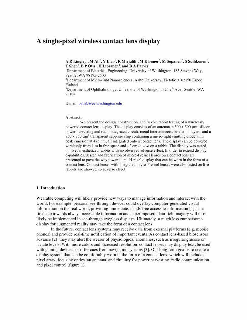
The process of forming electrical contacts involved three lithographic processes for lift-off, three metallizations, and plasma etching. AZ5214E photoresist (Capitol Scientific, Inc.) was used in image reversal mode to achieve resist sidewall undercut for each lift-off. Ni was evaporated to etch different LED pixel sizes because of its excellent etch selectivity during chlorine-based inductively coupled plasma etching. Chlorine-based plasma was used to etch a total of 800 nm, through the p-GaN and MQW stack and expose the n-GaN layer. P-metal contacts (Ni/Au/Ag/Au, 5/5/70/200 nm) were evaporated on the p-type mesa structures after a second photolithography. Ag was used to enhance light reflection from the contact side of the LED structure. Next, the n-contact metal (Ni/Al/Au, 20/860/200 nm) was deposited. The n- and p- metals were annealed between 400 and 500 ºC to improve the ohmic character of the contacts. Finally, the wafers were thinned to 250 µm by using lapping and grinding processes (CORWIL Technology Corporation) and diced into 750 x 750 µm2 chips prior to assembly on the contact lens platform. Figure 2 shows the LED growth stack and post growth etching and metallizaiton steps.
!"#$%&'()*$+('",$-('(##"./%01.0"'(%#"2$#*'13"
"
6"
"
Figure 2. Schematic depicting the micro-LED growth stack (left) and post-growth fabrication process (right). 2.3 Antenna.
Antenna design was constrained by contact lens size and eye physiology, and therefore a 5.0 mm radius loop antenna was used to harvest RF energy but leave the pupil unobstructed. Two factors determine the frequency of operation: 1) power received by the on-lens loop antenna, and 2) antenna-to-chip impedance matching.
To determine power received by the on-lens antenna, we began by simulating gain for a loop antenna having a 5.0 mm radius, 0.5 mm width, and 5.0 µm thickness (Advanced Design System, Momentum 3D Planar EM Simulator, Agilent Technologies, Inc.). The peak on-lens antenna received power was determined using simulated gain data and the Friis transmission equation, assuming perfect antenna-chip matching and values for safe transmit power, maximum likely antenna separation, and minimum transmit antenna gain. Figure 4 shows power received with 1.0 m separation using a 1.0 W power source and transmitting antenna gain of 1.76 dBi. In free space, modeled received power peaked at ~117 µW at approximately 2.0 GHz (figure 3). At lower frequencies, received power is limited by on-lens antenna efficiency, while path loss dominates at higher frequencies.
We also simulated the eyeball and the tear film with 1.0 cm and 5.0 µm of saline solution (relative permittivity = 74, conductivity = 0.47 S/m) below and above the antenna, respectively. Antenna received power is significantly reduced in this more realistic operational environment, In this case, the simulated maximum received power is ~12 µW (figure 3). Therefore, we expect operating distances, assuming equivalent power consumption, to be shorter on the eye than in free space. However, as contact lens and transmitting antenna separation decreases, near field interactions begin to dominate and more power is available. These simulation results confirm that only small amounts of power are available for operating electronic and photonic systems on-lens.

!"#$%&'()*$+('",$-('(##"./%01.0"'(%#"2$#*'13"
"
7"
"
Figure 3. Simulated received power from a 1.0 W source at a distance of 1.0 m on contact lens placed in free space (dashed line), and also with 5.0 µm of saline above the antenna and 1.0 cm of saline below the antenna to model the eye (solid line).
Impedance matching between chip and antenna can have significant impact on system performance. Typically, wireless systems have passive matching networks between chip and antenna to achieve maximum power transfer [19], improve power amplifier efficiency, or to provide voltage gain that improves the sensitivity of voltage-limited rectifiers. For an on-lens system, surface mount parts are prohibitively large, so the chip and antenna must be directly connected without an external matching network. Multiple rectifier stages are used in the on-lens chip to reduce the necessary RF input power needed to excite the LED.
In our case, adequate antenna-to-chip matching is possible without an external matching network. Simulations show an antenna self-resonance of ~3.6 GHz. The antenna can be capacitive or inductive, depending on whether it is operated above or below self-resonance, respectively. However, chip size limitations require that the power harvesting IC is capacitive. Hence, when operating below 3.6 GHz, chip capacitance (negative imaginary impedance) and antenna inductance (positive imaginary impedance) cancel and maximum power is transferred to the chip. The chip impedance is approximately 7! + 1.2 pF and the on-lens antenna has an inductance of 22 nH below the resonant frequency. Thus, resonant frequency of the antenna and chip system is approximately 980 MHz.
It is necessary to adhere to biological safety limits for exposure to non-ionizing radiation provided by the Institute for Electrical and Electronics Engineers (IEEE) and the International Committee on Non-ionizing Radiation Protection (ICNIRP). The ICNIRP set the basic requirement for exposure of the head and trunk for the general public at 2 Wkg-1 (up to 10 GHz), or a plane wave power density of 10 Wm-2 (2 – 300 GHz) [20]. The IEEE Standard C95.1-2005 places exposure limits at 2 Wkg-1 (100 kHz – 3 GHz) or 10 Wm-2 (2 GHz – 100 GHz). Research contained in the IEEE standard and a recent ICNIRP review [21] point toward thermally induced cataracts as the primary biological concern of RF exposure to the eye. Our aim is to remain well below the thresholds set by these standards during the normal operation of the contact lens system. 2.4 Contact Lens Template Fabrication. The antenna, electrical interconnects, electrical isolation, and pads for solder coating were fabricated directly on the contact lens. Polyethylene terephthalate (PET) was chosen as a substrate because of good chemical resistance, thermal stability during photolithography, and transparency.
First, 100 mm wafers with major and minor flats were cut from 25.4 cm x 25.4 cm x 100 µm sheets of polyethylene terephthalate (POLICROM, Inc.) using a CO2 laser cutter. The wafers were cleaned with sonication in acetone, isopropyl alcohol (IPA), deionized water, and then spin-rinse-dried. Next, AZ4620 (MicroChem Corp.) was spun (spread: 500 rpm, 100 rpm/s, 10 s, spin:

!"#$%&'()*$+('",$-('(##"./%01.0"'(%#"2$#*'13"
"
8"
"
4500 rpm, 1000 rpm/s, 30 s) and soft-baked (35 ºC, ramped to 70 ºC with a 10 min hold, and ramped to 35 ºC). Ultra-violet exposure was done in an ABM contact aligner for 35 s with I-line at 13 mW/cm2 and H-line at 25 mW/cm2. The wafers were developed in AZ400K (MicroChem Corp.) for 90 s. The wafers were plasma cleaned in a Branson barrel etcher for 3 min at 300 W, and immediately placed in an electron beam evaporator. A layer of Cr/Ni/Au (20, 80, 350 nm) was evaporated at 5 x 10⁻⁶ Torr. An acetone soak and short sonication facilitated metal lift-off. After lift-off, the wafers were rinsed in IPA, deionized water, and put through a spin-rinse-dry. Next, a ~2 µm layer of SU-8 2 was spun (spread: 500 rpm, 100 rpm/s, 10 s, spin: 3000 rpm, 300 rpm/s, 40 s), baked (35 ºC, ramp to 70 ºC, 10 min hold, ramp to 35 ºC), exposed for 20 s, and developed for 90 sec in SU-8 with agitation. Again, the wafers were rinsed in IPA, and sent through the spin-rinse-dry. Next, a 40 nm seed layer of Au was deposited using electron beam evaporation, and AZ4620 was patterned using the aforementioned method. Next, pulsed electroplating (1 ms on, 1 ms off) was used to plate ~ 5 µm of Au using a cyanide-based Pur-A-Gold® 401 formulation (Enthone-OMI Inc.). This electroplating step is necessary in order to produce more efficient antennas. The photoresist was removed in acetone, and the seed layer was etched in 5:1 (vol:vol) deionized H2O:Gold Etch TFA (Transene Company, Inc.). SU-8 25 was spun (spread: 500 rpm, 100 rpm/s, 10 s, spin: 2000 rpm, 300 rpm/s, 40 s), exposed for 30 s, and developed for 4 min in SU-8 developer. Blue dicing tape was placed on the back of the wafers, and individual contact lenses were cut out with CO2 laser cutting. Aluminum oxide sand paper (5 µm grit) was used to polish the contact lens edges after laser cutting. 2.5 Component Assembly and Molding.
We connected the LED and CMOS circuit to the lens in a manner similar to that presented in reference [22]. Prior to solder coating, the custom silicon IC (form MOSIS) aluminum pads were electrolessly plated with Ni and Au (CV Inc.). Lead-free, 60 ºC eutectic solder (Indium Corp., Indalloy 19) was used to coat the exposed pads on the template, microchips, and micro-LEDs. The solder was melted in a 100 mL beaker while immersed in ethylene glycol (EG). Next, 60 µL of HCl was added to the ethylene glycol to clean the solder surface. While the solder was heating, a solution of 25 mL of EG and 10 µL of HCl was prepared in a petri dish. Prior to coating, the EG used during heating was removed from the solder by pipette, and 10 mL of fresh EG was added along with 60 µL of HCl. Next, the silicon IC microchip, micro-LED chip, and template were coated with solder using a pipette and then placed in the petri dish. The silicon microchip and micro-LED chip were placed on the contact lens in their corresponding SU-8 25 wells using a microscope to observe the process. Next, the petri dish was heated to melt the solder, during which time components were aligned and connected to the contact lens interconnects and antenna. The petri dish was removed from the hot plate approximately 30 s after chip alignment. After cooling for 5 min, the contact lenses were soaked in IPA for 20 minutes, then rinsed in IPA and dried with nitrogen.
We used a hemispherical aluminum mold (radius = 7.1 mm) to obtain the desired lens curvature. The mold has a small hole drilled through the center exiting the side that is connected to a vacuum. We heated the mold and a metal ring with an inner diameter slightly less than the contact lens on hotplate set to 200 ºC. The vacuum was pulled, and then the contact lens was centered on the mold. We then placed the mold on an insulating surface, and the ring was used to slowly press the contact lens over the mold. After cooling, the contact lens was removed from the mold, cleaned with IPA, and dried with nitrogen. Lastly, we deposited a layer of parylene-C (~10 µm, Specialty Coating Systems, PDS 2010 Labcoater® 2) conformally over the contact lens for the purposes of biocompatibility and mechanical strength. The contacts lenses were sterilized in ethanol for 10 minutes and stored in a saline solution prior to testing on animals.
!"#$%&'()*$+('",$-('(##"./%01.0"'(%#"2$#*'13"
"
9"
"
2.6 Fresnel lens fabrication.
To extend the utility of the contact lens display, we plan to develop multi-pixel systems using matrix addressable micro-LED arrays and micro-Fresnel lenses to focus images onto the retina. We have developed micro-LED pixel arrays on small chips and tested their functionality. Although our first chips have only five or eight 80 µm pixels on a 750 x 750 µm2 chip, work by other groups verify the possibility of producing higher density arrays, for example with 22 µm pitch [23]. This suggests that it would be possible to place hundreds of pixels on a 500 x 500 µm2 LED array chip.
To investigate the integration of subsidiary lenses on contacts, we fabricated and tested micrometer-scale Fresnel lenses to focus LED output onto the retina. Fresnel lenses could be positioned on an LED chip opposite the active layers (i.e. on the back side of the handle wafer, as in figure 1(c)) or on the contact lens template for the same effect. In order to facilitate characterization, we fabricated Fresnel lenses on contact lens templates.
Fresnel lens parameters (e.g. focal length, zone radii, zone width) were calculated using modified Fresnel diffraction approximations, and simulations were performed to evaluate lens effectiveness. Fresnel micro lenses were fabricated using electron beam lithography (EBL) to pattern opaque metal rings on transparent polyethylene terephthalate. PET poses two sets of problems: first, PET can melt during fabrication, and second, it can generate adverse electrical charging during EBL. The following fabrication process was developed to eliminate these effects. First, the substrate was cleaned and 70 nm of Al was evaporated at 7.5 Å/s. This aluminum layer acted to dissipate charge during EBL, and also formed opaque Fresnel zones. Next, negative EBL resist AR-N 7700 (ALLRESIST GmbH) was spun onto the substrate for 45 seconds at 6000 rpm and soft baked at 85 ºC for 1 minute. Following exposure at ~8 µC/cm2 and post-bake at 100 ºC for 2 min, the samples were developed in AR 300-46 (ALLRESIST GmbH) for 60 seconds. Phosphoric acid etchant 80-16-4(65) was used for ~4.5 min to etch the aluminum. After aluminum etching and resist stripping, a thin layer of BGL-GZ-83 (PROFACTOR GmbH) was spun onto the samples to prevent scratching during tests.
!"#$%&'()*$+('",$-('(##"./%01.0"'(%#"2$#*'13"
"
:"
"
3. Results
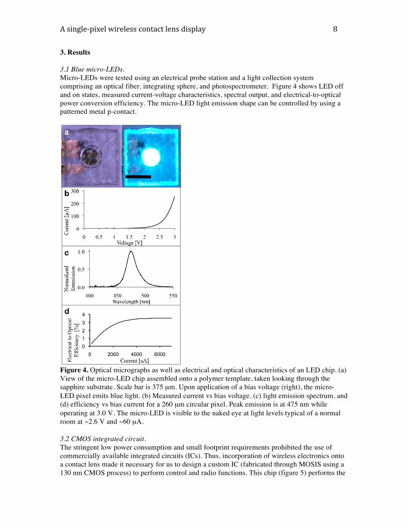
3.1 Blue micro-LEDs. Micro-LEDs were tested using an electrical probe station and a light collection system comprising an optical fiber, integrating sphere, and photospectrometer. Figure 4 shows LED off and on states, measured current-voltage characteristics, spectral output, and electrical-to-optical power conversion efficiency. The micro-LED light emission shape can be controlled by using a patterned metal p-contact.
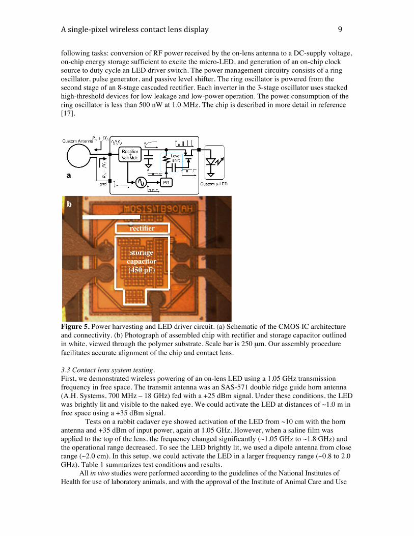
Figure 4. Optical micrographs as well as electrical and optical characteristics of an LED chip. (a) View of the micro-LED chip assembled onto a polymer template, taken looking through the sapphire substrate. Scale bar is 375 µm. Upon application of a bias voltage (right), the micro-LED pixel emits blue light. (b) Measured current vs bias voltage, (c) light emission spectrum, and (d) efficiency vs bias current for a 260 µm circular pixel. Peak emission is at 475 nm while operating at 3.0 V. The micro-LED is visible to the naked eye at light levels typical of a normal room at ~2.6 V and ~60 µA. 3.2 CMOS integrated circuit. The stringent low power consumption and small footprint requirements prohibited the use of commercially available integrated circuits (ICs). Thus, incorporation of wireless electronics onto a contact lens made it necessary for us to design a custom IC (fabricated through MOSIS using a 130 nm CMOS process) to perform control and radio functions. This chip (figure 5) performs the
!"#$%&'()*$+('",$-('(##"./%01.0"'(%#"2$#*'13"
"
;"
"
following tasks: conversion of RF power received by the on-lens antenna to a DC-supply voltage, on-chip energy storage sufficient to excite the micro-LED, and generation of an on-chip clock source to duty cycle an LED driver switch. The power management circuitry consists of a ring oscillator, pulse generator, and passive level shifter. The ring oscillator is powered from the second stage of an 8-stage cascaded rectifier. Each inverter in the 3-stage oscillator uses stacked high-threshold devices for low leakage and low-power operation. The power consumption of the ring oscillator is less than 500 nW at 1.0 MHz. The chip is described in more detail in reference [17].
Figure 5. Power harvesting and LED driver circuit. (a) Schematic of the CMOS IC architecture and connectivity. (b) Photograph of assembled chip with rectifier and storage capacitor outlined in white, viewed through the polymer substrate. Scale bar is 250 µm. Our assembly procedure facilitates accurate alignment of the chip and contact lens. 3.3 Contact lens system testing.
First, we demonstrated wireless powering of an on-lens LED using a 1.05 GHz transmission frequency in free space. The transmit antenna was an SAS-571 double ridge guide horn antenna (A.H. Systems, 700 MHz – 18 GHz) fed with a +25 dBm signal. Under these conditions, the LED was brightly lit and visible to the naked eye. We could activate the LED at distances of ~1.0 m in free space using a +35 dBm signal.
Tests on a rabbit cadaver eye showed activation of the LED from ~10 cm with the horn antenna and +35 dBm of input power, again at 1.05 GHz. However, when a saline film was applied to the top of the lens, the frequency changed significantly (~1.05 GHz to ~1.8 GHz) and the operational range decreased. To see the LED brightly lit, we used a dipole antenna from close range (~2.0 cm). In this setup, we could activate the LED in a larger frequency range (~0.8 to 2.0 GHz). Table 1 summarizes test conditions and results. All in vivo studies were performed according to the guidelines of the National Institutes of Health for use of laboratory animals, and with the approval of the Institute of Animal Care and Use

!"#$%&'()*$+('",$-('(##"./%01.0"'(%#"2$#*'13"
"
<="
"
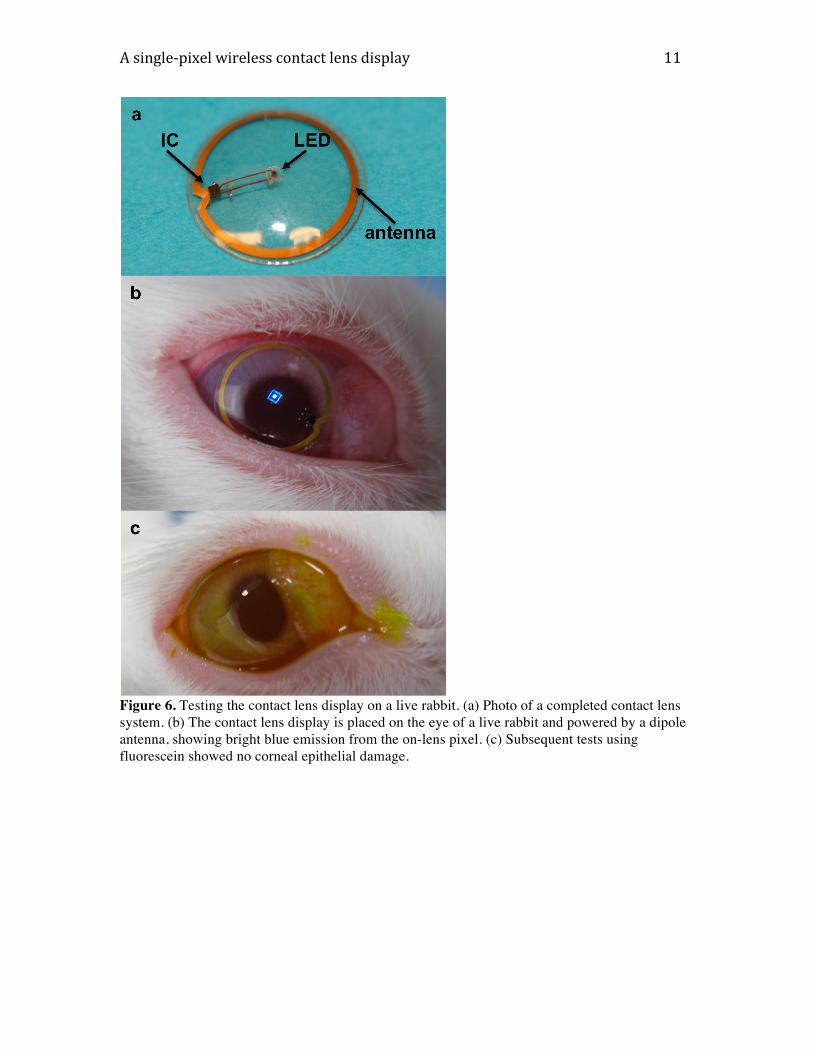
Committee of the University of Washington (Protocol # UW4139-01). All exams were conducted in the University of Washington vivarium designed with maximal comfort for the rabbits, and all examination equipment was portable to the rabbit “bed-side”. All in vivo evaluations were performed under general anesthesia. Female New Zealand White Rabbits (mean wt. 2.5kg) underwent general anesthesia with 5% induction of isoflurane and oxygen, which were maintained at 2% during the in vivo studies. Artificial tears were applied frequently to insure hydration. The prototype contact lens was well-fitted to the rabbit ocular surface (figure 6(b)). The micro-LED indicator was activated periodically and remained in vivo for up to 40 minutes.
We evaluated the effect of wearing the contact lens display on the rabbit cornea using portable slit lamp biomicroscopy and pachymetry. Additionally, topical fluorescein was applied to the corneal surface using a dropper and the eye was visually examined for potential corneal abrasion, thermal burn or corneal edema as a result of in vivo testing. Such damage would result in corneal surface roughness, causing the fluorescein to accumulate. Figure 6(c) demonstrates a healthy corneal epithelial layer after testing, showing no fluorescein streaks or cloudiness resulting from thermal burns or corneal edema.
!"#$%&'()*$+('",$-('(##"./%01.0"'(%#"2$#*'13"
"
<<"
"
Figure 6. Testing the contact lens display on a live rabbit. (a) Photo of a completed contact lens system. (b) The contact lens display is placed on the eye of a live rabbit and powered by a dipole antenna, showing bright blue emission from the on-lens pixel. (c) Subsequent tests using fluorescein showed no corneal epithelial damage.

!"#$%&'()*$+('",$-('(##"./%01.0"'(%#"2$#*'13"
"
<4"
"
Table 1. Contact lens testing summary.
3.4 Fresnel lenses.
To characterize the Fresnel lenses, a Nikon TE2000 Eclipse inverted optical microscope and a Hamamatsu ORCA-ER monochrome CCD camera were used to characterize the Fresnel lenses. Our Fresnel lenses were placed on a glass slide, with the rings facing the microscope objective, and a 200 mm pinhole was placed 56 mm above the lens. The microscope was focused on the lens surface, and the focal plane was slowly adjusted until the brightest spot was observed. Distances were measured using the focus knob on the microscope. For a lens with a diameter of 108 mm, the focal length was measured to be 62 mm. Figure 7(a) and 7(b) show the simulated and measured intensity distributions, respectively, at the focal plane for a lens we constructed. After fabrication and characterization, we molded and parylene coated the lenses (figure 7(c)), and then tested them in vivo on rabbits using procedures outlined above (figure 7(d) and 7(e)).
Figure 7. Micro-Fresnel lenses. (a) Simulated intensity profile at the focal plane of the lens. The z-axis units are arbitrary. (b) Measured intensity profile at the focal plane of the lens. (c) Optical

!"#$%&'()*$+('",$-('(##"./%01.0"'(%#"2$#*'13"
"
<5"
"
microscope image of a micro-Fresnel lens integrated on a contact lens. (d) Photograph of a contact lens with fifteen micro-Fresnel lenses placed on an anesthetized rabbit. No adverse effects were observed on the eye. (e) Close-up view of 3 x 5 array of Fresnel lenses on rabbit. 4. Discussion We have demonstrated the operation of a contact lens display powered by a remote radio-frequency transmitter in free space and on a live rabbit. The demonstration verifies that antennas, radio chips, control circuitry, and micrometer-scale light sources can be integrated into a contact lens. Although our display has only a single controllable pixel, the demonstration of all the technology components and subsystems indicates that in principle, it is possible to produce a higher resolution display in the form factor of a contact lens that can be remotely powered and controlled. We have also provided the first proof-of-concept technology demonstrations for producing a multi-pixel and in-focus image on a contact lens by demonstrating that multi-pixel micro-LED array chips on transparent substrates can be made and micrometer-scale Fresnel lenses can be integrated into a contact lens. The demonstration of Fresnel lenses on contact lenses points towards the potential of integrating other passive and active micro-optical components on a contact lens for vision correction and enhancement.
Significant improvements are necessary to produce fully functional, remotely powered, high-resolution displays. Although we could power our system in free space from more than a meter, on the rabbit eye the operating distance was reduced to the cm-range. Matching, interface, and absorption losses are likely causes of the limited operational distance. We are working to improve matching losses, and to ensure that power received by the contact lens is maximized at the frequency of best antenna-to-chip matching. We are working also to optimize LED efficiency and duty cycling in order to reduce power consumption of individual pixels, which will be required for multi-pixel designs. Although only microwatt levels of power are available on the contact lens, as most of the light generated by the optical components directly enters the eye, the display could be very efficient and can generate a clearly visible image consuming very little power. PET has been our substrate of choice thus far for contact lens construction due to the ease of performing some of the microfabrication processes; however, PET has poor oxygen permeability and its extended use could lead to lactate build up and corneal swelling [24]. It will be necessary to adapt our processes to more common rigid gas permeable or hydrogel contact lens materials. This work is currently in progress in our laboratory. We have demonstrated the integration of blue and red micron-scale light sources on contact lenses. The integration of green emitting micron-scale light sources must be achieved in order to fully extend the color gamut.
We believe it may be possible to develop more complex systems with higher resolution, color, range, and computing power. Depending on the complexity of the contact lens display, various uses might be envisioned. For example, a display with a single controllable pixel can be used in gaming, training, or giving warnings to the hearing impaired. A display with a handful of pixels can be used for giving directional information and a display with yet more pixels may be used for showing basic textual information such as short emails or text messages. Although a high resolution, full-color, stand-alone contact lens display might be many years away, the technology demonstrations to this date depict a clear roadmap containing a number of useful devices on the way that can be feasibly produced in the near to medium terms. If such displays are successfully deployed, they may fundamentally change the nature of interaction between humans and visual information.

!"#$%&'()*$+('",$-('(##"./%01.0"'(%#"2$#*'13"
"
<6"
"
Acknowledgements
We would like to acknowledge the National Science Foundation (the EFRI program), the Defense Advanced Research Projects Agency, the Microsoft Corporation, the Nokia Foundation, the Aalto MIDE program, and Research to Prevent Blindness for their financial support. We would also like to thank Dr Sami Suihkonen for his help with LED design, Roman Khakimow and Igor Shavrin for simulation and characterization of Fresnel lenses, and the staff at the Washington Technology Center Microfabrication Laboratory for their help in process development. References
[1] Billinghurst M and Starner T 1999 Wearable devices: new ways to manage information Computer 32 57-64. [2] Lahdesmaki I, Shum A and Parviz B A 2010 Possibilities for continuous glucose monitoring by a functional contact lens Instrum. and Meas., IEEE Trans. on 13 14-17.
[3] Parviz B A 2009 For your eye only Spectrum, IEEE 46 36-41. [4] Robinson D 1963 A method of measuring eye movement using a scleral search coil in a magnetic field Bio-medical Electronics, IEEE Trans. on 10 137-145. [5] Kim K, Lee S and Kim H 2004 A wireless measurement system for three-dimensional ocular movement using the magnetic contact lens sensing technique IEMBS '04. 26th Annual Inter.
Conf. of the IEEE 1 2287-2289. [6] Badugu R, Lakowicz J R and Geddes C D 2004 Noninvasive continuous monitoring of physiological glucose using a monosaccharide-sensing contact lens Anal. Chem. 76 610-618. [7] March W F, Mueller A and Herbrechtsmeier P 2004 Clinical trial of a noninvasive contact lens glucose sensor Diabetes Technol. Ther. 6 782-789. [8] Domschke A, March W F, Kabilan S and Lowe C 2006 Initial clinical testing of a holographic non-invasive contact lens glucose sensor Diabetes Technol. Ther. 8 89-93. [9] Yao H, Shum A, Cowan M, Lahdesmaki I and Parviz B A 2011 A contact lens with embedded sensor for monitoring tear glucose level Biosensors and Bioelectronics 26 3290-3296. [10] Chu M et al. 2011 Soft contact lens biosensor for in situ monitoring of tear glucose as non-invasive blood sugar assessment Talanta 83 960-965. [11] Kinn J B and Tell R A 1973 A liquid-crystal contact-lens device for measurement of corneal temperature Biomedical Engineering, IEEE Trans. on BME 20 387-388. [12] Scott V, Tarassenko L, Glynn C and Hill A 1996 Contact lens oximetry: a valid concept?
Pulse Oximetry: A Critical Appraisal, IEE Colloquium on 3/1-3/3. [13] Leonardi M, Pitchon E M, Bertsch A, Renaud P and Mermoud A 2007 Wireless contact lens sensor for intraocular pressure monitoring: assessment on enucleated pig eyes Acta
Ophthalmologica 87 433-437.

!"#$%&'()*$+('",$-('(##"./%01.0"'(%#"2$#*'13"
"
<7"
"
[14] Szurman P, et al. 2005 Experimental implantation and long-term testing of an intraocular vision aid in rabbits Archives of Ophthalmology 123 964-969. [15] Phillips A J 2007 in Contact Lenses: 5th Edition, ed Phillips A J, Speedwell L (Elsevier, New York) pp. 218. [16] Saeedi E, Kim S and Parviz B A 2007 Self-assembled inorganic micro-display on plastic MEMS, IEEE 20th Internation Conference on 755-758. [17] Pandey J, et al. 2010 A fully integrated RF-powered contact lens with a single element display Biomedical Circuits and Systems, IEEE Trans. on 4 454-461. [18] Nakamura S 2002 III-V nitride-based LEDs and lasers: current status and future opportunities Electron Devices Meeting, 2000. IEDM Technical Digest. International pp. 9-11. [19] Barnett R E, Liu J and Lazar S 2009 A RF to DC Voltage Conversion Model for Multi-stage Rectifiers in UHF RFID Transponders Solid-State Circuits, IEEE Journal of 44 354-370. [20] Ahlbom A, et al. 1998 Guidelines for limiting exposure to time-varying electric, magnetic, and electromagnetic fields (up to 300 GHz) Health Phys. 74 494-522. [21] Swerdlow A 2010 in Exposure to high frequency electromagnetic fields, biological effects
and health consequences (100 kHz-300 GHz), eds Vecchia P, et al. (International Committee on Non-Ionizing Radiation Protection, Oberschlei!heim) pp. 208-211. [22] Stauth S A and Parviz B A 2006 Self-assembled single-crystal silicon circuits on plastic Proceedings of the National Academy of Sciences 103 13922-13927. [23] Choi H W, Jeon C W and Dawson M D 2004 High-Resolution 128 x 96 Nitride Microdisplay IEEE Electron Device Letters 25 277-279. [24] Sweeney D F, Stretton S, Fonn D, Swarbrick H A and Holden B A 2007 in Contact Lenses:
5th Edition, ed Phillips A J, Speedwell L (Elsevier, New York) pp. 273-274.