a single-chip bidirectional neural interface with high
TRANSCRIPT

IEEE JOURNAL OF SOLID-STATE CIRCUITS, VOL. 55, NO. 7, JULY 2020 1749
A Single-Chip Bidirectional Neural Interface WithHigh-Voltage Stimulation and Adaptive Artifact
Cancellation in Standard CMOSJohn P. Uehlin , Member, IEEE, William Anthony Smith , Member, IEEE,
Venkata Rajesh Pamula , Member, IEEE, Eric P. Pepin, Steve Perlmutter,Visvesh Sathe, Member, IEEE, and Jacques Christophe Rudell, Senior Member, IEEE
Abstract— A single-chip, bidirectional brain–computerinterface (BBCI) enables neuromodulation through simultaneousneural recording and stimulation. This article presents aprototype BBCI application-specified integrated circuit (ASIC)consisting of a 64-channel time-multiplexed recording front-end, an area-optimized four-channel high-voltage compliantstimulator, and electronics to support the concurrent multi-channel stimulus artifact cancellation. Stimulator powergeneration is integrated on a chip, providing ±11-V compliancefrom low-voltage supplies with a resonant charge pump. High-frequency (∼3 GHz) self-resonant clocking is used to reducethe pumping capacitor area while suppressing the associatedswitching losses. A 32-tap least mean square (LMS)-based digitaladaptive filter achieves 60-dB artifact suppression, enablingsimultaneous neural stimulation and recording. The entire chipoccupies 4 mm2 in a 65-nm low power (LP) process and ispowered by 2.5-/1.2-V supplies, dissipating 205 µW in recordingand 142 µW in the stimulation and cancellation back-ends. Thestimulation output drivers achieve 31% dc–dc efficiency at amaximum output power of 24 mW.
Index Terms— Artifact cancellation, brain–computer inter-faces, electrical stimulation, neural recording, time-division mul-tiplexing.
I. INTRODUCTION
REALIZATIONS of small-form factor, ultralow-powerbidirectional brain–computer interfaces (BBCIs) will
enable the treatment of chronic neurophysiological disordersand allow new modes to investigate brain function. Neuralstimulators have been shown to effectively alleviate the symp-toms of Parkinson’s disease [1], epilepsy [2], depression [3],
Manuscript received December 2, 2019; revised March 3, 2020; acceptedApril 14, 2020. Date of publication May 15, 2020; date of current versionJune 29, 2020. This article was approved by Guest Editor Lucien J. Breems.This work was supported by Medtronic and the Center for Neurotech-nology, under NSF Award Number EEC-1028725. (Corresponding author:John P. Uehlin.)
John P. Uehlin is with NoiseFigure Research, Renton, WA 98057 USA(e-mail: [email protected]).
Venkata Rajesh Pamula, Visvesh Sathe, and Jacques Christophe Rudellare with the Electrical and Computer Engineering Department, Universityof Washington, Seattle, WA 98195 USA.
William Anthony Smith and Eric P. Pepin are with Space ExplorationTechnologies (SpaceX), Redmond, WA 98053 USA.
Steve Perlmutter is with the Physiology and Biophysics Department,University of Washington, Seattle, WA 98195 USA, and also with theWashington National Primate Research Center, University of Washington,Seattle, WA 98195 USA.
Color versions of one or more of the figures in this article are availableonline at http://ieeexplore.ieee.org.
Digital Object Identifier 10.1109/JSSC.2020.2991524
Fig. 1. Example of the integrated bidirectional neural interface.
and obsessive-compulsive disorder [4]. The development ofclosed-loop neural interfaces with simultaneous recording andstimulation capabilities will increase therapy effectiveness byadapting to real-time measurements of the modulated neuraltissue without input from a practitioner [5]. In addition, asufficiently complex closed-loop interface could be used toreanimate the damaged neural tissue or drive neuroprosthe-ses with sensorimotor feedback [6]. In addition to clinicalapplications, simultaneous stimulation and sensing opens newresearch opportunities for neuroscientists, including the studyof neural plasticity [7] and low-latency neural mapping [8].
In order to increase the efficacy and accessibility ofpotentially life-changing treatments, BBCI implants must bedeveloped with minimal cost, size, and power use. A single-chip BBCI implementation minimizes the area and powerconsumption by reducing the number of interconnects. In addi-tion, standard scaled-CMOS technology offers dense andpower-efficient digital devices for complex BBCI therapyprotocols. A single-chip CMOS BBCI front-end requires theintegration of recording, stimulation, and power generationelectronics on the same substrate along with a sophisticateddigital back-end. Fig. 1 shows the components of a single-chip BBCI front-end. In addition, resilient operation in chronicimplants requires the capability to continuously adapt to aslowly varying environment to maintain the desired stimulationand recording function.
Critical challenges remain before the vision of implantablesingle-chip BBCI neural interfaces becomes a reality; thisarticle addresses two such challenges. First, the voltagesgenerated at the stimulator–electrode interface (>10 V)
0018-9200 © 2020 IEEE. Personal use is permitted, but republication/redistribution requires IEEE permission.See https://www.ieee.org/publications/rights/index.html for more information.
Authorized licensed use limited to: University of Washington Libraries. Downloaded on October 13,2020 at 00:15:12 UTC from IEEE Xplore. Restrictions apply.

1750 IEEE JOURNAL OF SOLID-STATE CIRCUITS, VOL. 55, NO. 7, JULY 2020
regularly exceed the acceptable gate oxide breakdown limits(<1.5 V) for reliable operation in advanced, scaled CMOStechnologies [9]. Second, the electrical stimulation createsin-band artifacts that are several orders of magnitude largerthan the signals targeted by neural recording front-ends(∼100 mV versus ∼100 μV) [10].
Recent implementations use a variety of techniques toaddress stimulation artifacts. One approach simply migratesto a high-voltage (HV) CMOS process, where the traditionalcurrent/voltage-driving structures can readily tolerate highstimulation voltages. The recording channels have beendesigned in HV processes that are naturally immune tolarge voltage swings due to stimulation artifacts [11].However, the large core devices in these processes areless suited for efficient integration of digital processingalgorithms as will be demanded of future generation BBCIs.Other implementations mitigate the stimulation artifacts byoverdesigning the record front-end dynamic range. Theseapproaches quantize both the large stimulus artifact andthe underlying neural signals [12]–[16], relying on a DSPback-end to digitally remove the artifact. The front-endoverdesign can create a recording non-linearity (voltage-controlled oscillator (VCO)-based ADCs [12]) and introducesarea, complexity, or power-consumption tradeoffs. Artifactsare most efficiently mitigated using the adaptive mixed-signalfeedback in the front- and back-ends [17]–[19]. The proposedmultiplexed canceller is optimized to reduce the powerconsumption, using less than 50 nW per artifact channelduring continuous operation, and less than 8 nW per channelfor a standard 10-Hz stimulation rate.
This article achieves HV stimulation compliance (±11 V)using stacked circuits in low-voltage scaled CMOS. Thestacked driver architecture enables constant-current stimula-tion through a large range of electrode impedances from thesame chip as a complex, efficient digital back-end. Chargepumps are typically used to create above-VDD stimulationvoltages, and the pumping capacitors dominate the systemarea. This article minimizes the charge pump area usingintegrated inductors to reclaim power while operating at a highcharge pump clock frequency to reduce the area overhead.The proposed stimulator implements the first GHz-clockedcharge pump to achieve aggressive area reduction in neuralstimulation, while relying on resonance to effectively mitigatethe adverse efficiency impact from this miniaturization.
The HV stimulators are integrated with the time-divisionmultiplexed recording architecture from [20] and [21]. Therecording system uses closed-loop adaptive feedback for stim-ulus artifact cancellation on multiple channels. The cancellercomputation hardware is also time-multiplexed to reducepower and area consumption. The resulting monolithic 65-nmCMOS chip includes all the necessary components to allowsimultaneous 64-channel recording and 4-channel stimulationfor BBCI-clinical applications. This article is an elaborationof the work presented in [22].
This article is organized as follows. Section II discusses theoverall system architecture. Section III elaborates on the reso-nant H-bridge stimulator and analysis of power generation andefficiency. Section IV briefly describes the integrated recording
channels. Section V describes the design and optimization ofthe adaptive artifact canceller. Section VI provides the systemand circuit implementation details, as well as benchtop andin vivo measurements. Concluding remarks are presented inSection VII.
II. SYSTEM OVERVIEW
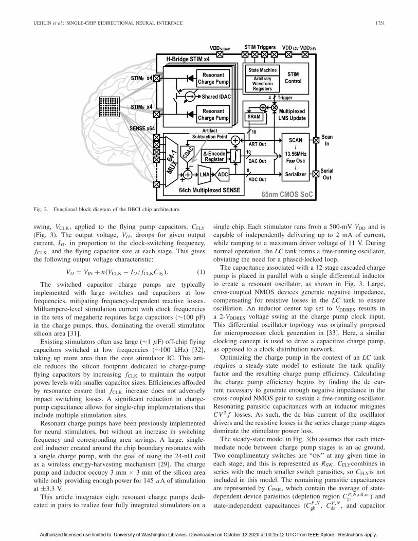
A block diagram of the full system implemented is shownin Fig. 2. Four integrated H-bridge stimulators are indepen-dently tunable with digitally programmable current wave-forms. The resonant charge pumps generate up to 11 V to driveup to 2 mA of sink-regulated current through the electrode–tissue load. The shared IDAC is switched between the twosides of the H-bridge.
A time-multiplexed, delta-encoded recording front-end [20],[21] records 64 channels using a single recording chain.A multiplexer routes all channels to a shared input capacitiveDAC (CDAC), front-end amplifier, and successive approxima-tion register (SAR) ADC. A digital integration loop incrementsthe CDAC at the recording amplifier input to subtract low-frequency signal content. Such a delta-encoded loop creates afrequency-shaped dynamic range well suited for the coloredspectral shape of neural signals [23]. The system targets64-channel electrocorticography (ECoG) recordings at 2 kS/s.
The digital back-end implements an adaptive artifact cancel-lation filter. A simplified least mean square (LMS) algorithmprocesses the recording output and stimulator control signalsinto a time-domain reconstruction of unwanted stimulus arti-facts. The artifact voltage is subtracted using the CDAC at therecording amplifier input. The canceller computation hardwareassociated with adapting the filter is time-multiplexed betweenchannels, and the filter coefficients are stored using an on-chip-dedicated SRAM.
III. RESONANT CHARGE PUMP H-BRIDGE STIMULATOR
A. HV Stimulation
Constant-current stimulation pulses create large voltages atthe load interface due to high electrode impedances [24]. Thisarticle uses an H-bridge stimulator topology to double thevoltage compliance range for a given maximum output voltage.The stimulator output is ground-referenced, and each differ-ential side has a dedicated charge pump to supply positivevoltage as needed to each side of the load. The charge pumpsare dynamically enabled to generate only as much voltageas necessary to drive the current through the tissue–electrodeload. Specifics of the constant-current voltage control loop canbe found in [25]. Compared with a fixed-supply stimulator[11], [26]–[28], dynamic voltage supplies save energy whenstimulating below the maximum output voltage [29].
B. Resonant Charge Pump Voltage Supplies
This article uses a modified version of the cross-coupledswitched capacitor charge pump presented in [30], whichis well suited for use in triple-well, deep sub-micrometerintegrated CMOS processes. The charge pump draws currentfrom an input voltage, VIN, and adds the voltage proportionalto the number of cascaded stages, n, and the clock voltage
Authorized licensed use limited to: University of Washington Libraries. Downloaded on October 13,2020 at 00:15:12 UTC from IEEE Xplore. Restrictions apply.
UEHLIN et al.: SINGLE-CHIP BIDIRECTIONAL NEURAL INTERFACE 1751
Fig. 2. Functional block diagram of the BBCI chip architecture.
swing, VCLK, applied to the flying pump capacitors, CFLY
(Fig. 3). The output voltage, VO , droops for given outputcurrent, IO , in proportion to the clock-switching frequency,fCLK, and the flying capacitor size at each stage. This givesthe following output voltage characteristic:
VO = VIN + n(VCLK − IO/ fCLKCfly). (1)
The switched capacitor charge pumps are typicallyimplemented with large switches and capacitors at lowfrequencies, mitigating frequency-dependent reactive losses.Milliampere-level stimulation current with clock frequenciesin the tens of megahertz requires large capacitors (∼100 pF)in the charge pumps, thus, dominating the overall stimulatorsilicon area [31].
Existing stimulators often use large (∼1 μF) off-chip flyingcapacitors switched at low frequencies (∼100 kHz) [32],taking up more area than the core stimulator IC. This arti-cle reduces the silicon footprint dedicated to charge-pumpflying capacitors by increasing fCLK to maintain the outputpower levels with smaller capacitor sizes. Efficiencies affordedby resonance ensure that fCLK increase does not adverselyimpact switching losses. A significant reduction in charge-pump capacitance allows for single-chip implementations thatinclude multiple stimulation sites.
Resonant charge pumps have been previously implementedfor neural stimulators, but without an increase in switchingfrequency and corresponding area savings. A large, single-coil inductor created around the chip boundary resonates witha single charge pump, with the goal of using the 24-nH coilas a wireless energy-harvesting mechanism [29]. The chargepump and inductor occupy 3 mm × 3 mm of the silicon areawhile only providing enough power for 145 μA of stimulationat ±3.3 V.
This article integrates eight resonant charge pumps dedi-cated in pairs to realize four fully integrated stimulators on a
single chip. Each stimulator runs from a 500-mV VDD and iscapable of independently delivering up to 2 mA of current,while ramping to a maximum driver voltage of 11 V. Duringnormal operation, the LC tank forms a free-running oscillator,obviating the need for a phased-locked loop.
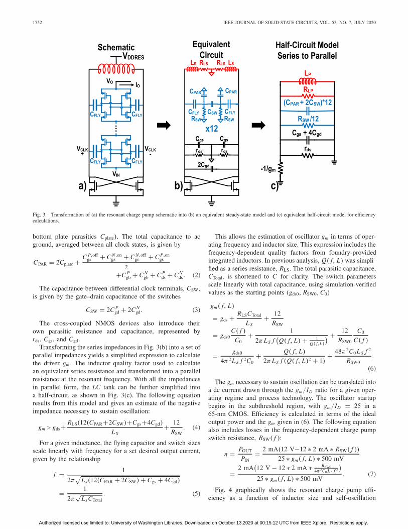
The capacitance associated with a 12-stage cascaded chargepump is placed in parallel with a single differential inductorto create a resonant oscillator, as shown in Fig. 3. Large,cross-coupled NMOS devices generate negative impedance,compensating for resistive losses in the LC tank to ensureoscillation. An inductor center tap set to VDDRES results ina 2-VDDRES voltage swing at the charge pump clock input.This differential oscillator topology was originally proposedfor microprocessor clock generation in [33]. Here, a similarclocking concept is used to drive a capacitive charge pump,as opposed to a clock distribution network.
Optimizing the charge pump in the context of an LC tankrequires a steady-state model to estimate the tank qualityfactor and the resulting charge pump efficiency. Calculatingthe charge pump efficiency begins by finding the dc cur-rent necessary to generate enough negative impedance in thecross-coupled NMOS pair to sustain a free-running oscillator.Resonating parasitic capacitances with an inductor mitigatesCV 2 f losses. As such, the dc bias current of the oscillatordrivers and the resistive losses in the series charge pump stagesdominate the stimulator power loss.
The steady-state model in Fig. 3(b) assumes that each inter-mediate node between charge pump stages is an ac ground.Two complimentary switches are “ON” at any given time ineach stage, and this is represented as RSW. CFLYcombines inseries with the much smaller switch parasitics, so CFLYis notincluded in this model. The remaining parasitic capacitancesare represented by CPAR, which contain the average of state-dependent device parasitics (depletion region C P,N,off,on
gs ) andstate-independent capacitances (C P,N
gb , C P,Nds , and capacitor
Authorized licensed use limited to: University of Washington Libraries. Downloaded on October 13,2020 at 00:15:12 UTC from IEEE Xplore. Restrictions apply.
1752 IEEE JOURNAL OF SOLID-STATE CIRCUITS, VOL. 55, NO. 7, JULY 2020
Fig. 3. Transformation of (a) the resonant charge pump schematic into (b) an equivalent steady-state model and (c) equivalent half-circuit model for efficiencycalculations.
bottom plate parasitics Cplate). The total capacitance to acground, averaged between all clock states, is given by
CPAR = 2Cplate + C P,offgs + C N,on
gs + C N,offgs + C P,on
gs
2+C P
gb + C Ngb + C P
ds + C Nds . (2)
The capacitance between differential clock terminals, CSW,is given by the gate–drain capacitance of the switches
CSW = 2C Pgd + 2C N
gd. (3)
The cross-coupled NMOS devices also introduce theirown parasitic resistance and capacitance, represented byrds, Cgs, and Cgd.
Transforming the series impedances in Fig. 3(b) into a set ofparallel impedances yields a simplified expression to calculatethe driver gm . The inductor quality factor used to calculatean equivalent series resistance and transformed into a parallelresistance at the resonant frequency. With all the impedancesin parallel form, the LC tank can be further simplified intoa half-circuit, as shown in Fig. 3(c). The following equationresults from this model and gives an estimate of the negativeimpedance necessary to sustain oscillation:
gm >gds+ RLS(12(CPAR+2CSW)+Cgs+4Cgd)
L S+ 12
RSW. (4)
For a given inductance, the flying capacitor and switch sizesscale linearly with frequency for a set desired output current,given by the relationship
f = 1
2π√
Ls(12(CPAR + 2CSW) + Cgs + 4Cgd)
= 1
2π√
LsCTotal. (5)
This allows the estimation of oscillator gm in terms of oper-ating frequency and inductor size. This expression includes thefrequency-dependent quality factors from foundry-providedintegrated inductors. In previous analysis, Q( f, L) was simpli-fied as a series resistance, RLS. The total parasitic capacitance,CTotal, is shortened to C for clarity. The switch parametersscale linearly with total capacitance, using simulation-verifiedvalues as the starting points (gds0, RSW0, C0)
gm( f, L)
= gds + RLSCTotal
L S+ 12
RSW
= gds0C( f )
C0+ 1
2π L S f(Q( f, L) + 1
Q( f,L)
) + 12
RSW0
C0
C( f )
= gds0
4π2 L S f 2C0+ Q( f, L)
2π L S f (Q( f, L)2 + 1)+ 48π2C0 L S f 2
RSW0.
(6)
The gm necessary to sustain oscillation can be translated intoa dc current drawn through the gm/ID ratio for a given oper-ating regime and process technology. The oscillator startupbegins in the subthreshold region, with gm/ID = 25 in a65-nm CMOS. Efficiency is calculated in terms of the idealoutput power and the gm given in (6). The following equationalso includes losses in the frequency-dependent charge pumpswitch resistance, RSW( f ):
η = POUT
PIN= 2 mA(12 V−12 ∗ 2 mA ∗ RSW( f ))
25 ∗ gm( f, L) ∗ 500 mV
= 2 mA(12 V − 12 ∗ 2 mA ∗ RSW0
4π2C0 L S f 2
)
25 ∗ gm( f, L) ∗ 500 mV. (7)
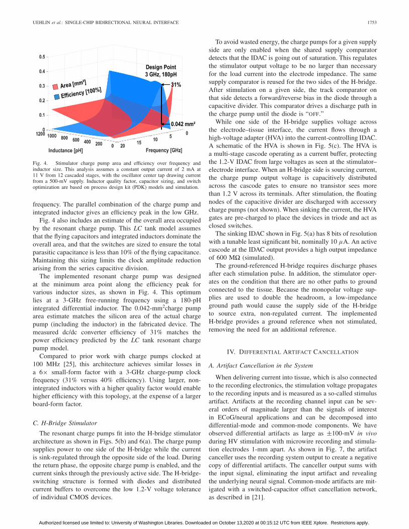
Fig. 4 graphically shows the resonant charge pump effi-ciency as a function of inductor size and self-oscillation
Authorized licensed use limited to: University of Washington Libraries. Downloaded on October 13,2020 at 00:15:12 UTC from IEEE Xplore. Restrictions apply.
UEHLIN et al.: SINGLE-CHIP BIDIRECTIONAL NEURAL INTERFACE 1753
Fig. 4. Stimulator charge pump area and efficiency over frequency andinductor size. This analysis assumes a constant output current of 2 mA at11 V from 12 cascaded stages, with the oscillator center tap drawing currentfrom a 500-mV supply. Inductor quality factor, capacitor sizing, and switchoptimization are based on process design kit (PDK) models and simulation.
frequency. The parallel combination of the charge pump andintegrated inductor gives an efficiency peak in the low GHz.
Fig. 4 also includes an estimate of the overall area occupiedby the resonant charge pump. This LC tank model assumesthat the flying capacitors and integrated inductors dominate theoverall area, and that the switches are sized to ensure the totalparasitic capacitance is less than 10% of the flying capacitance.Maintaining this sizing limits the clock amplitude reductionarising from the series capacitive division.
The implemented resonant charge pump was designedat the minimum area point along the efficiency peak forvarious inductor sizes, as shown in Fig. 4. This optimumlies at a 3-GHz free-running frequency using a 180-pHintegrated differential inductor. The 0.042-mm2charge pumparea estimate matches the silicon area of the actual chargepump (including the inductor) in the fabricated device. Themeasured dc/dc converter efficiency of 31% matches thepower efficiency predicted by the LC tank resonant chargepump model.
Compared to prior work with charge pumps clocked at100 MHz [25], this architecture achieves similar losses ina 6× small-form factor with a 3-GHz charge-pump clockfrequency (31% versus 40% efficiency). Using larger, non-integrated inductors with a higher quality factor would enablehigher efficiency with this topology, at the expense of a largerboard-form factor.
C. H-Bridge Stimulator
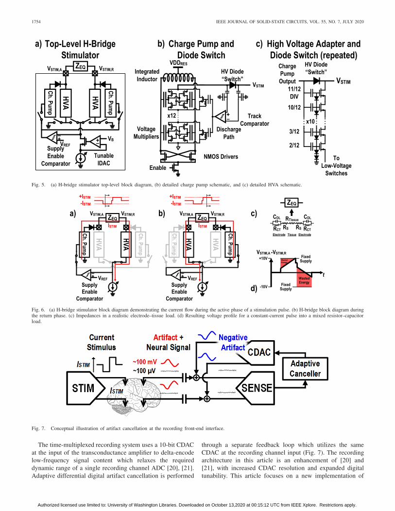
The resonant charge pumps fit into the H-bridge stimulatorarchitecture as shown in Figs. 5(b) and 6(a). The charge pumpsupplies power to one side of the H-bridge while the currentis sink-regulated through the opposite side of the load. Duringthe return phase, the opposite charge pump is enabled, and thecurrent sinks through the previously active side. The H-bridge-switching structure is formed with diodes and distributedcurrent buffers to overcome the low 1.2-V voltage toleranceof individual CMOS devices.
To avoid wasted energy, the charge pumps for a given supplyside are only enabled when the shared supply comparatordetects that the IDAC is going out of saturation. This regulatesthe stimulator output voltage to be no larger than necessaryfor the load current into the electrode impedance. The samesupply comparator is reused for the two sides of the H-bridge.After stimulation on a given side, the track comparator onthat side detects a forward/reverse bias in the diode through acapacitive divider. This comparator drives a discharge path inthe charge pump until the diode is “OFF.”
While one side of the H-bridge supplies voltage acrossthe electrode–tissue interface, the current flows through ahigh-voltage adapter (HVA) into the current-controlling IDAC.A schematic of the HVA is shown in Fig. 5(c). The HVA isa multi-stage cascode operating as a current buffer, protectingthe 1.2-V IDAC from large voltages as seen at the stimulator–electrode interface. When an H-bridge side is sourcing current,the charge pump output voltage is capacitively distributedacross the cascode gates to ensure no transistor sees morethan 1.2 V across its terminals. After stimulation, the floatingnodes of the capacitive divider are discharged with accessorycharge pumps (not shown). When sinking the current, the HVAgates are pre-charged to place the devices in triode and act asclosed switches.
The sinking IDAC shown in Fig. 5(a) has 8 bits of resolutionwith a tunable least significant bit, nominally 10 μA. An activecascode at the IDAC output provides a high output impedanceof 600 M� (simulated).
The ground-referenced H-bridge requires discharge phasesafter each stimulation pulse. In addition, the stimulator oper-ates on the condition that there are no other paths to groundconnected to the tissue. Because the monopolar voltage sup-plies are used to double the headroom, a low-impedanceground path would cause the supply side of the H-bridgeto source extra, non-regulated current. The implementedH-bridge provides a ground reference when not stimulated,removing the need for an additional reference.
IV. DIFFERENTIAL ARTIFACT CANCELLATION
A. Artifact Cancellation in the System
When delivering current into tissue, which is also connectedto the recording electronics, the stimulation voltage propagatesto the recording inputs and is measured as a so-called stimulusartifact. Artifacts at the recording channel input can be sev-eral orders of magnitude larger than the signals of interestin ECoG/neural applications and can be decomposed intodifferential-mode and common-mode components. We haveobserved differential artifacts as large as ±100-mV in vivoduring HV stimulation with microwire recording and stimula-tion electrodes 1-mm apart. As shown in Fig. 7, the artifactcanceller uses the recording system output to create a negativecopy of differential artifacts. The canceller output sums withthe input signal, eliminating the input artifact and revealingthe underlying neural signal. Common-mode artifacts are mit-igated with a switched-capacitor offset cancellation network,as described in [21].
Authorized licensed use limited to: University of Washington Libraries. Downloaded on October 13,2020 at 00:15:12 UTC from IEEE Xplore. Restrictions apply.
1754 IEEE JOURNAL OF SOLID-STATE CIRCUITS, VOL. 55, NO. 7, JULY 2020
Fig. 5. (a) H-bridge stimulator top-level block diagram, (b) detailed charge pump schematic, and (c) detailed HVA schematic.
Fig. 6. (a) H-bridge stimulator block diagram demonstrating the current flow during the active phase of a stimulation pulse. (b) H-bridge block diagram duringthe return phase. (c) Impedances in a realistic electrode–tissue load. (d) Resulting voltage profile for a constant-current pulse into a mixed resistor–capacitorload.
Fig. 7. Conceptual illustration of artifact cancellation at the recording front-end interface.
The time-multiplexed recording system uses a 10-bit CDACat the input of the transconductance amplifier to delta-encodelow-frequency signal content which relaxes the requireddynamic range of a single recording channel ADC [20], [21].Adaptive differential digital artifact cancellation is performed
through a separate feedback loop which utilizes the sameCDAC at the recording channel input (Fig. 7). The recordingarchitecture in this article is an enhancement of [20] and[21], with increased CDAC resolution and expanded digitaltunability. This article focuses on a new implementation of
Authorized licensed use limited to: University of Washington Libraries. Downloaded on October 13,2020 at 00:15:12 UTC from IEEE Xplore. Restrictions apply.

UEHLIN et al.: SINGLE-CHIP BIDIRECTIONAL NEURAL INTERFACE 1755
Fig. 8. Behavioral block diagram of a full LMS-based artifact canceller.
an on-chip differential cancellation technique, realized usingan ensemble of adaptively trained impulse response filters forvarious stim/record channel pairs.
B. FIR-Based Adaptive Filters
Fig. 8 shows an adaptive canceller algorithm where the finiteimpulse response (FIR) filter coefficients are adapted using anLMS algorithm. For an FIR-based canceller implementation,the filter input signal, x(n), is a time-domain representationof the stimulation current pulse. This input is convolved witha set of coefficients, {c0, cN } to create the filter output, y(n),to create the FIR filter transfer function
y(n) =N∑
i=0
ci x(n − i). (8)
The coefficients are trained based on the recording systemoutput, e(n), which is the residual artifact and neural signalremaining after subtracting the FIR filter’s output from theinput signal, y �(n). The FIR coefficients can be trained withan LMS algorithm, where the update coefficient, μ, tunesthe step size at each update interval. Coefficients adapt thealgorithm as
cN (n + 1) = cN (n) + μe(n)x(n − N). (9)
Implementing the full LMS/FIR adaptive filter shownin Fig. 8 requires power and area-intensive hardware. Eachtap of the FIR filter requires two multipliers, one adder, andtwo delay cells. This cost is multiplied by the number ofimplemented filter channels. This article proposes a simpli-fication of this adaptive filter that dramatically reduces thenecessary hardware for similar functionality and performanceacross multiple channels.
C. Impulse-Based Adaptive Filter
The end goal of the adaptive filter is a time-domain repre-sentation of the stimulation voltage artifact. The FIR coeffi-cients in the previously described approach are an intermediatestep, quantifying the channel which changes the stimulatoroutput current into the voltage artifact at the recording channelinput. This intermediate step can be removed by changing thefilter input into a discrete delta function. The FIR coefficientscan be trained to a time-domain representation of the artifactvoltage waveform, with several added benefits: most multipli-cands become unity, the updated hardware can be multiplexed,and the tapped delay line can be removed.
With a discrete delta input signal propagating through theFIR filter, only one tap of the filter is active at a time. Thisremoves the need for a sum at the filter output. In addition,the multiplication of each tap coefficient with the delayedfilter input, x(n), is replaced with multiplication by zero orunity as the discrete impulse input propagates through thefilter. For N samples after stimulation onset at n0, the filtersimplifies to
y(n)=N∑
i=0
ciδ(n − n0 − i)=cn−n0, 0 ≤ n − n0 ≤ N. (10)
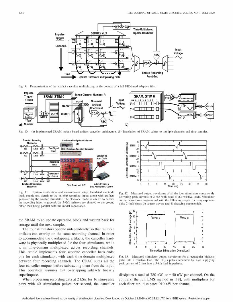
In this implementation, the same LMS update algorithmin (9) updates one coefficient at a time. Given the high-speed logic available in a scaled CMOS and the low sam-pling frequencies necessary for adequately representing neuralsignals, it is possible to time-domain multiplex one set ofLMS update hardware between all the filter taps. Furthermore,the time-domain multiplexed recording architecture lends itselfwell to the multiplexing of filter hardware between multiplestimulation–recording channel pairs. A representation of thismultiplexing is shown in Fig. 9. While the filter coefficientsare adapting, the scaling of the error signal used in theLMS adaptation is simplified to a division via a bitwiseshift. The update operation first rotates through the recordingchannels before progressing down the time-domain taps ofthe impulse response filter, as indicated by the helical spiralin Fig. 9. Somewhat noteworthy is the fact that althoughthe adaptation hardware is being reused between differentchannels, the filter response for each stim-s’ sense combinationis adapted uniquely. Each artifact produced at one stimulationsite propagates to each recoding site and has a unique artifactresponse and a dedicated set of coefficients. The distributionof the unique stored artifact values is shown in Fig. 10(b).
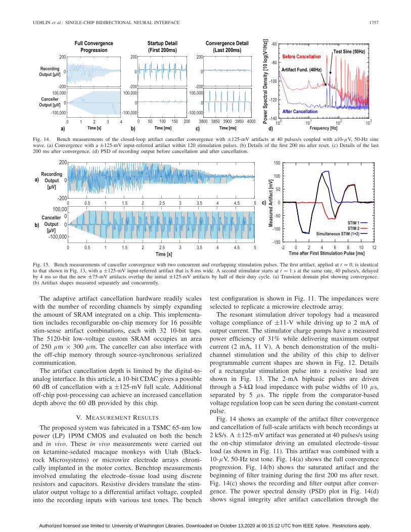
The filter can be further simplified to remove the tappeddelay line. Only one tap is active at a time, so the onlyfunctionality required is the storage and recall of filter values.This article uses a writable lookup table to replace the FIRfilter, removing the power-consuming delay line. An integratedSRAM stores the filter values. The artifact samples, yR,S(n)in Fig. 10, are equivalent to the coefficients in (10), cn−n0 .The artifact samples are indexed by the filter tap number,n, recording channel, R, and stimulation channel, S. Thepreviously stored coefficient for a given index is read out of
Authorized licensed use limited to: University of Washington Libraries. Downloaded on October 13,2020 at 00:15:12 UTC from IEEE Xplore. Restrictions apply.
1756 IEEE JOURNAL OF SOLID-STATE CIRCUITS, VOL. 55, NO. 7, JULY 2020
Fig. 9. Demonstration of the artifact canceller multiplexing in the context of a full FIR-based adaptive filter.
Fig. 10. (a) Implemented SRAM lookup-based artifact canceller architecture. (b) Translation of SRAM values to multiple channels and time samples.
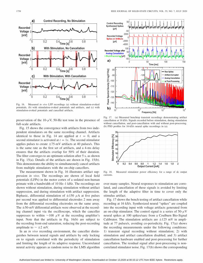
Fig. 11. System verification and measurement setup. Emulated electrodeloads couple test signals to the on-chip recording inputs along with artifactsgenerated by the on-chip stimulator. The electrode model is altered to dc biasthe recording input to ground; the 5-G� resistors are shunted to the groundrather than being parallel with the model capacitance.
the SRAM to an update operation block and written back forstorage until the next sample.
The four stimulators operate independently, so that multipleartifacts can overlap on the same recording channel. In orderto accommodate the overlapping artifacts, the canceller hard-ware is physically multiplexed for the four stimulators, whileit is time-domain multiplexed across recording channels.This article implements four separate canceller back-ends,one for each stimulator, with each time-domain multiplexedbetween four recording channels. The CDAC sums all thefour canceller outputs before subtracting them from the input.This operation assumes that overlapping artifacts linearlysuperimpose.
When processing recording data at 2 kS/s for 16 stim-sensepairs with 40 stimulation pulses per second, the canceller
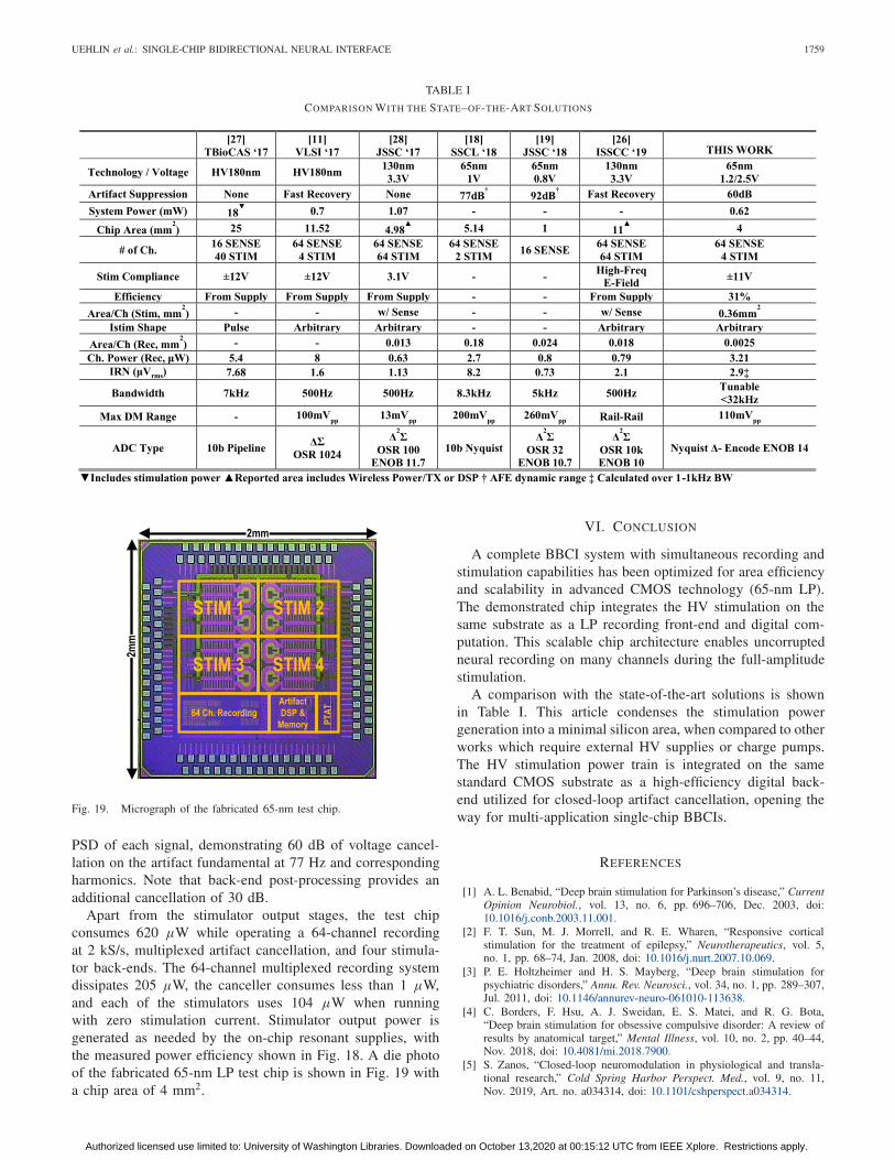
Fig. 12. Measured output waveforms of all the four stimulators concurrentlydelivering peak currents of 2 mA with equal 5-k� resistive loads. Stimulatorcurrent waveforms programmed with the following shapes: 1) rising exponen-tials; 2) half-sines; 3) square waves; and 4) decaying exponentials.
Fig. 13. Measured stimulator output waveforms for a rectangular biphasicpulse into a resistive load. The 10-μs pulses separated by 5-μs supplyingpeak current of 2 mA into a 5-k� load impedance.
dissipates a total of 780 nW, or ∼50 nW per channel. On thecontrary, the full LMS method in [18], with multipliers foreach filter tap, dissipates 910 nW per channel.
Authorized licensed use limited to: University of Washington Libraries. Downloaded on October 13,2020 at 00:15:12 UTC from IEEE Xplore. Restrictions apply.
UEHLIN et al.: SINGLE-CHIP BIDIRECTIONAL NEURAL INTERFACE 1757
Fig. 14. Bench measurements of the closed-loop artifact canceller convergence with ±125-mV artifacts at 40 pulses/s coupled with a10-μV, 50-Hz sinewave. (a) Convergence with a ±125-mV input-referred artifact within 120 stimulation pulses. (b) Details of the first 200 ms after reset. (c) Details of the last200 ms after convergence. (d) PSD of recording output before cancellation and after cancellation.
Fig. 15. Bench measurements of canceller convergence with two concurrent and overlapping stimulation pulses. The first artifact, applied at t = 0, is identicalto that shown in Fig. 13, with a ±125-mV input-referred artifact that is 8-ms wide. A second stimulator starts at t = 1 s at the same rate, 40 pulses/s, delayedby 4 ms so that the new ±75-mV artifacts overlap the initial ±125-mV artifacts by half of their duty cycle. (a) Transient domain plot showing convergence.(b) Artifact shapes measured separately and concurrently.
The adaptive artifact cancellation hardware readily scaleswith the number of recording channels by simply expandingthe amount of SRAM integrated on a chip. This implementa-tion includes reconfigurable on-chip memory for 16 possiblestim-sense artifact combinations, each with 32 10-bit taps.The 5120-bit low-voltage custom SRAM occupies an areaof 250 μm × 300 μm. The canceller can also interface withthe off-chip memory through source-synchronous serializedcommunication.
The artifact cancellation depth is limited by the digital-to-analog interface. In this article, a 10-bit CDAC gives a possible60 dB of cancellation with a ±125-mV full scale. Additionaloff-chip post-processing can achieve an increased cancellationdepth above the 60 dB provided by this chip.
V. MEASUREMENT RESULTS
The proposed system was fabricated in a TSMC 65-nm lowpower (LP) 1P9M CMOS and evaluated on both the benchand in vivo. These in vivo measurements were carried outon ketamine-sedated macaque monkeys with Utah (Black-rock Microsystems) or microwire electrode arrays chroni-cally implanted in the motor cortex. Benchtop measurementsinvolved emulating the electrode–tissue load using discreteresistors and capacitors. Resistive dividers translate the stim-ulator output voltage to a differential artifact voltage, coupledinto the recording inputs with various test tones. The bench
test configuration is shown in Fig. 11. The impedances wereselected to replicate a microwire electrode array.
The resonant stimulation driver topology had a measuredvoltage compliance of ±11-V while driving up to 2 mA ofoutput current. The stimulator charge pumps have a measuredpower efficiency of 31% while delivering maximum outputcurrent (2 mA, 11 V). A bench demonstration of the multi-channel stimulation and the ability of this chip to deliverprogrammable current shapes are shown in Fig. 12. Detailsof a rectangular stimulation pulse into a resistive load areshown in Fig. 13. The 2-mA biphasic pulses are driventhrough a 5-k� load impedance with pulse widths of 10 μs,separated by 5 μs. The ripple from the comparator-basedvoltage regulation loop can be seen during the constant-currentpulse.
Fig. 14 shows an example of the artifact filter convergenceand cancellation of full-scale artifacts with bench recordings at2 kS/s. A ±125-mV artifact was generated at 40 pulses/s usingthe on-chip stimulator driving an emulated electrode–tissueload (as shown in Fig. 11). This artifact was combined with a10-μV, 50-Hz test tone. Fig. 14(a) shows the full convergenceprogression. Fig. 14(b) shows the saturated artifact and thebeginning of filter training during the first 200 ms after reset.Fig. 14(c) shows the recording and filter output after conver-gence. The power spectral density (PSD) plot in Fig. 14(d)shows signal integrity after artifact cancellation through the
Authorized licensed use limited to: University of Washington Libraries. Downloaded on October 13,2020 at 00:15:12 UTC from IEEE Xplore. Restrictions apply.
1758 IEEE JOURNAL OF SOLID-STATE CIRCUITS, VOL. 55, NO. 7, JULY 2020
Fig. 16. Measured in vivo LFP recordings (a) without stimulation-evokedpotentials, (b) with stimulation-evoked potentials and artifacts, and (c) withstimulation-evoked potentials and cancelled artifacts.
preservation of the 10-μV, 50-Hz test tone in the presence offull-scale artifacts.
Fig. 15 shows the convergence with artifacts from two inde-pendent stimulators on the same recording channel. Artifactsidentical to those in Fig. 14 are applied at t = 0, and asecond stimulator is activated at t = 1s. The second stimulatorapplies pulses to create ±75-mV artifacts at 40 pulses/s. Thisis the same rate as the first set of artifacts, and a 4-ms delayensures that the artifacts overlap for 50% of their duration.The filter converges to an optimum solution after 5 s, as shownin Fig. 15(a). Details of the artifacts are shown in Fig. 15(b).This demonstrates the ability to simultaneously cancel artifactsfrom multiple stimulators with the on-chip cancellers.
The measurement shown in Fig. 16 illustrates artifact sup-pression in vivo. The recordings are shown of local fieldpotentials (LFPs) in the motor cortex of a sedated non-humanprimate with a bandwidth of 10 Hz–1 kHz. The recordings areshown without stimulation, during stimulation without artifactsuppression, and during stimulation with artifact suppression.Biphasic, differential stimulation of ±150 μA at five pulsesper second was applied to differential electrodes 2 mm awayfrom the differential recording electrodes on the same array.The ±50-mV differential artifacts were observed at the record-ing channel input via the oscilloscope, which the cancellersuppresses to within ∼100 μV at the recording amplifier’sinput. Note that the artifacts in Fig. 16(b) are subject tothe recording front-end saturation, reducing the post-recordingamplitude to ∼ ±2 mV.
In an in vivo recording environment, the canceller distin-guishes between neural signals and artifacts by only lockingon to signals correlated with the periodicity of stimulationand limiting the length of its adaptive response. Uncorrelatedneural activity appears as random noise to the LMS algorithm
Fig. 17. (a) Measured benchtop transient recordings demonstrating artifactcancellation at 16 kS/s. Signals recorded before stimulation, during stimulationwithout cancellation, and post-cancellation with and without post-processing.(b) PSD profiles for 16-kS/s neural spike recordings in (a).
Fig. 18. Measured stimulator power efficiency for a range of dc outputcurrents.
over many samples. Neural responses to stimulation are corre-lated, and cancellation of these signals is avoided by limitingthe length of the adaptive filter in time to cover only thestimulus artifact.
Fig. 17 shows the bench testing of artifact cancellation whilerecording at 16 kS/s. Synthesized neural “spikes” are coupledinto the recording input with voltage artifacts generated froman on-chip stimulator. The control signal is a series of 50-μVneural spikes at 100 spikes/saec from a Coulburn Bio-SignalCalibrator. The stimulation artifacts are ±125 mV in ampli-tude at 77 pulses/s, avoiding co-periodicity. Fig. 17(a) showsthe recording measurements under the following conditions:1) transient signal recording without stimulation; 2) withstimulation and artifact cancellation disabled; and 3) artifactcancellation hardware enabled and post-processing for furthercancellation. The residual signal after post-processing is non-correlated stimulator noise. Fig. 17(b) shows the corresponding
Authorized licensed use limited to: University of Washington Libraries. Downloaded on October 13,2020 at 00:15:12 UTC from IEEE Xplore. Restrictions apply.
UEHLIN et al.: SINGLE-CHIP BIDIRECTIONAL NEURAL INTERFACE 1759
TABLE I
COMPARISON WITH THE STATE–OF-THE-ART SOLUTIONS
Fig. 19. Micrograph of the fabricated 65-nm test chip.
PSD of each signal, demonstrating 60 dB of voltage cancel-lation on the artifact fundamental at 77 Hz and correspondingharmonics. Note that back-end post-processing provides anadditional cancellation of 30 dB.
Apart from the stimulator output stages, the test chipconsumes 620 μW while operating a 64-channel recordingat 2 kS/s, multiplexed artifact cancellation, and four stimula-tor back-ends. The 64-channel multiplexed recording systemdissipates 205 μW, the canceller consumes less than 1 μW,and each of the stimulators uses 104 μW when runningwith zero stimulation current. Stimulator output power isgenerated as needed by the on-chip resonant supplies, withthe measured power efficiency shown in Fig. 18. A die photoof the fabricated 65-nm LP test chip is shown in Fig. 19 witha chip area of 4 mm2.
VI. CONCLUSION
A complete BBCI system with simultaneous recording andstimulation capabilities has been optimized for area efficiencyand scalability in advanced CMOS technology (65-nm LP).The demonstrated chip integrates the HV stimulation on thesame substrate as a LP recording front-end and digital com-putation. This scalable chip architecture enables uncorruptedneural recording on many channels during the full-amplitudestimulation.
A comparison with the state-of-the-art solutions is shownin Table I. This article condenses the stimulation powergeneration into a minimal silicon area, when compared to otherworks which require external HV supplies or charge pumps.The HV stimulation power train is integrated on the samestandard CMOS substrate as a high-efficiency digital back-end utilized for closed-loop artifact cancellation, opening theway for multi-application single-chip BBCIs.
REFERENCES
[1] A. L. Benabid, “Deep brain stimulation for Parkinson’s disease,” CurrentOpinion Neurobiol., vol. 13, no. 6, pp. 696–706, Dec. 2003, doi:10.1016/j.conb.2003.11.001.
[2] F. T. Sun, M. J. Morrell, and R. E. Wharen, “Responsive corticalstimulation for the treatment of epilepsy,” Neurotherapeutics, vol. 5,no. 1, pp. 68–74, Jan. 2008, doi: 10.1016/j.nurt.2007.10.069.
[3] P. E. Holtzheimer and H. S. Mayberg, “Deep brain stimulation forpsychiatric disorders,” Annu. Rev. Neurosci., vol. 34, no. 1, pp. 289–307,Jul. 2011, doi: 10.1146/annurev-neuro-061010-113638.
[4] C. Borders, F. Hsu, A. J. Sweidan, E. S. Matei, and R. G. Bota,“Deep brain stimulation for obsessive compulsive disorder: A review ofresults by anatomical target,” Mental Illness, vol. 10, no. 2, pp. 40–44,Nov. 2018, doi: 10.4081/mi.2018.7900.
[5] S. Zanos, “Closed-loop neuromodulation in physiological and transla-tional research,” Cold Spring Harbor Perspect. Med., vol. 9, no. 11,Nov. 2019, Art. no. a034314, doi: 10.1101/cshperspect.a034314.
Authorized licensed use limited to: University of Washington Libraries. Downloaded on October 13,2020 at 00:15:12 UTC from IEEE Xplore. Restrictions apply.
1760 IEEE JOURNAL OF SOLID-STATE CIRCUITS, VOL. 55, NO. 7, JULY 2020
[6] C. T. Moritz, S. I. Perlmutter, and E. E. Fetz, “Direct control of paralysedmuscles by cortical neurons,” Nature, vol. 456, no. 7222, pp. 639–642,Dec. 2008, doi: 10.1038/nature07418.
[7] Y. Nishimura, S. I. Perlmutter, R. W. Eaton, and E. E. Fetz, “Spike-timing-dependent plasticity in primate corticospinal connections inducedduring free behavior,” Neuron, vol. 80, no. 5, pp. 1301–1309, Dec. 2013,doi: 10.1016/j.neuron.2013.08.028.
[8] C. J. Keller, C. J. Honey, P. Mégevand, L. Entz, I. Ulbert,and A. D. Mehta, “Mapping human brain networks with cortico-cortical evoked potentials,” Phil. Trans. Roy. Soc. B, Biol. Sci.,vol. 369, no. 1653, Oct. 2014, Art. no. 20130528, doi: 10.1098/rstb.2013.0528.
[9] C. Günter, J. Delbeke, and M. Ortiz-Catalan, “Safety of long-termelectrical peripheral nerve stimulation: Review of the state of theart,” J. NeuroEng. Rehabil., vol. 16, no. 1, p. 13, Dec. 2019, doi:10.1186/s12984-018-0474-8.
[10] A. Zhou, B. C. Johnson, and R. Müller, “Toward true closed-loop neuromodulation: Artifact-free recording during stimulation,”Current Opinion Neurobiol., vol. 50, pp. 119–127, Jun. 2018, doi:10.1016/j.conb.2018.01.012.
[11] B. C. Johnson et al., “An implantable 700 μW 64-channel neuromodu-lation IC for simultaneous recording and stimulation with rapid artifactrecovery,” in Proc. Symp. VLSI Circuits, Jun. 2017, pp. C48–C49, doi:10.23919/VLSIC.2017.8008543.
[12] W. Jiang, V. Hokhikyan, H. Chandrakumar, V. Karkare, andD. Markovic, “A ±50-mV linear-input-range VCO-based neural-recording front-end with digital nonlinearity correction,” IEEE J.Solid-State Circuits, vol. 52, no. 1, pp. 173–184, Jan. 2017, doi:10.1109/JSSC.2016.2624989.
[13] H. Chandrakumar and D. Markovic, “An 80-mVpp linear-input range,1.6-G� input impedance, low-power chopper amplifier for closed-loopneural recording that is tolerant to 650-mVpp common-mode interfer-ence,” IEEE J. Solid-State Circuits, vol. 52, no. 11, pp. 2811–2828,Nov. 2017, doi: 10.1109/JSSC.2017.2753824.
[14] M. R. Pazhouhandeh, H. Kassiri, A. Shoukry, I. Wesspapir, P. Carlen,and R. Genov, “Artifact-tolerant opamp-less delta-modulated bidirec-tional neuro-interface,” in Proc. IEEE Symp. VLSI Circuits, Jun. 2018,pp. 127–128, doi: 10.1109/VLSIC.2018.8502286.
[15] H. Jeon, J.-S. Bang, Y. Jung, I. Choi, and M. Je, “A high DR, DC-coupled, time-based neural-recording IC with degeneration R-DAC forbidirectional neural interface,” IEEE J. Solid-State Circuits, vol. 54,no. 10, pp. 2658–2670, Oct. 2019, doi: 10.1109/JSSC.2019.2930903.
[16] D. Rozgic et al., “A 0.338 cm3, artifact-free, 64-contact neuromodula-tion platform for simultaneous stimulation and sensing,” IEEE Trans.Biomed. Circuits Syst., vol. 13, no. 1, pp. 38–55, Feb. 2019, doi:10.1109/TBCAS.2018.2889040.
[17] A. E. Mendrela et al., “A bidirectional neural interface circuit with activestimulation artifact cancellation and cross-channel common-mode noisesuppression,” IEEE J. Solid-State Circuits, vol. 51, no. 4, pp. 955–965,Apr. 2016, doi: 10.1109/JSSC.2015.2506651.
[18] S. Jung, P. Kwon, D. Piech, M. Maharbiz, J. Rabaey, and E. Alon,“A 2.7-μ w neuromodulation AFE with 200 mVpp differential-modestimulus artifact canceler including on-chip LMS adaptation,” IEEESolid-State Circuits Lett., vol. 1, no. 10, pp. 194–197, Oct. 2018, doi:10.1109/LSSC.2019.2908090.
[19] C. Kim, S. Joshi, H. Courellis, J. Wang, C. Miller, andG. Cauwenberghs, “Sub-μ vrms -noise sub-μ W/Channel ADC-directneural recording with 200-mV/ms transient recovery through predictivedigital autoranging,” IEEE J. Solid-State Circuits, vol. 53, no. 11,pp. 3101–3110, Nov. 2018, doi: 10.1109/JSSC.2018.2870555.
[20] W. A. Smith, J. P. Uehlin, S. I. Perlmutter, J. C. Rudell, and V. S. Sathe,“A scalable, highly-multiplexed delta-encoded digital feedback ECoGrecording amplifier with common and differential-mode artifact sup-pression,” in Proc. Symp. VLSI Circuits, Jun. 2017, pp. C172–C173,doi: 10.23919/VLSIC.2017.8008470.
[21] J. P. Uehlin, W. A. Smith, V. R. Pamula, S. I. Perlmutter, J. C. Rudell,and V. S. Sathe, “A 0.0023 mm2/ch. delta-encoded, time-division mul-tiplexed mixed-signal ECoG recording architecture with stimulus arti-fact suppression,” IEEE Trans. Biomed. Circuits Syst., vol. 14, no. 2,pp. 319–331, Apr. 2020.
[22] J. Uehlin, W. A. Smith, V. Rajesh Pamula, S. Perlmutter, V. Sathe, andJ. C. Rudell, “A bidirectional brain computer interface with 64-channelrecording, resonant stimulation and artifact suppression in standard65 nm CMOS,” in Proc. IEEE 45th Eur. Solid State Circuits Conf. (ESS-CIRC), Sep. 2019, pp. 77–80, doi: 10.1109/ESSCIRC.2019.8902911.
[23] G. Baranauskas et al., “Origins of 1/f2 scaling in the power spectrumof intracortical local field potential,” J. Neurophysiol., vol. 107, no. 3,pp. 984–994, Feb. 2012, doi: 10.1152/jn.00470.2011.
[24] W. Franks, I. Schenker, P. Schmutz, and A. Hierlemann, “Impedancecharacterization and modeling of electrodes for biomedical applications,”IEEE Trans. Biomed. Eng., vol. 52, no. 7, pp. 1295–1302, Jul. 2005, doi:10.1109/TBME.2005.847523.
[25] E. Pepin, J. Uehlin, D. Micheletti, S. I. Perlmutter, and J. C. Rudell, “Ahigh-voltage compliant, electrode-invariant neural stimulator front-endin 65 nm bulk-CMOS,” in Proc. Conf., 42nd Eur. Solid-State CircuitsConf. (ESSCIRC), Sep. 2016, pp. 229–232, doi: 10.1109/ESSCIRC.2016.7598284.
[26] M. R. Pazhouhandeh et al., “22.8 adaptively clock-boosted auto-rangingresponsive neurostimulator for emerging neuromodulation applications,”in IEEE Int. Solid-State Circuits Conf. (ISSCC) Dig. Tech. Papers,Feb. 2019, pp. 374–376, doi: 10.1109/ISSCC.2019.8662458.
[27] Y.-K. Lo et al., “A fully integrated wireless SoC for motorfunction recovery after spinal cord injury,” IEEE Trans. Bio-med. Circuits Syst., vol. 11, no. 3, pp. 497–509, Jun. 2017, doi:10.1109/TBCAS.2017.2679441.
[28] H. Kassiri et al., “Rail-to-Rail-Input dual-radio 64-channel closed-loop neurostimulator,” IEEE J. Solid-State Circuits, vol. 52, no. 11,pp. 2793–2810, Nov. 2017, doi: 10.1109/JSSC.2017.2749426.
[29] S. Ha, C. Kim, J. Park, G. Cauwenberghs, and P. P. Mercier, “A fullyintegrated RF-powered energy-replenishing current-controlled stimula-tor,” IEEE Trans. Biomed. Circuits Syst., vol. 13, no. 1, pp. 191–202,Feb. 2019, doi: 10.1109/TBCAS.2018.2881800.
[30] R. Pelliconi, D. Iezzi, A. Baroni, M. Pasotti, and P. L. Rolandi, “Powerefficient charge pump in deep submicron standard CMOS technology,”IEEE J. Solid-State Circuits, vol. 38, no. 6, pp. 1068–1071, Jun. 2003,doi: 10.1109/JSSC.2003.811991.
[31] Z. Luo, M.-D. Ker, T.-Y. Yang, and W.-H. Cheng, “A digitally dynamicpower supply technique for 16-channel 12 V-Tolerant stimulator realizedin a 0.18-μm 1.8-V/3.3-V low-voltage CMOS process,” IEEE Trans.Biomed. Circuits Syst., vol. 11, no. 5, pp. 1087–1096, Oct. 2017, doi:10.1109/TBCAS.2017.2713122.
[32] A. Abdi, H. S. Kim, and H.-K. Cha, “A high-voltage generation charge-pump IC using input voltage modulated regulation for neural implantdevices,” IEEE Trans. Circuits Syst. II, Exp. Briefs, vol. 66, no. 3,pp. 342–346, Mar. 2019, doi: 10.1109/TCSII.2018.2852360.
[33] W. C. Athas, N. Tzartzanis, L. J. Svensson, and L. Peterson, “A low-power microprocessor based on resonant energy,” IEEE J. Solid-State Circuits, vol. 32, no. 11, pp. 1693–1701, Nov. 1997, doi:10.1109/4.641689.
John P. Uehlin (Member, IEEE) received the B.S.and M.S. degrees in electrical engineering and thePh.D. degree in electrical and computer engineeringfrom the University of Washington, Seattle, WA,USA, in 2013, 2017, and 2020, respectively.
He is currently designing RF/mixed-signal cir-cuits with NoiseFigure Research, Tukwila, WA. Hisresearch interests include low-power circuit designand neural interfaces.
William Anthony Smith (Member, IEEE) receivedthe B.S. degree in electrical engineering from theUniversity of Texas at Austin, Austin, TX, USA,in 2007, and the M.S. degree in electrical engineer-ing from the University of Utah, Salt Lake City,UT, USA, in 2011, and the Ph.D. degree in electri-cal engineering from the University of Washington,Seattle, WA, USA, in 2017.
He has previously held industry positions at AMD,Austin, TX, USA, Spansion, Sunnyvale, CA, USA,and Fathom Computing, Palo Alto, CA, USA. He is
currently employed by Space Exploration Technologies (SpaceX), Redmond,WA, as an RFIC Design Engineer, where he designs millimeter-wave siliconfor the Starlink Broadband Satellite Internet Project.
Authorized licensed use limited to: University of Washington Libraries. Downloaded on October 13,2020 at 00:15:12 UTC from IEEE Xplore. Restrictions apply.
UEHLIN et al.: SINGLE-CHIP BIDIRECTIONAL NEURAL INTERFACE 1761
Venkata Rajesh Pamula (Member, IEEE) receivedthe B.Tech. degree in electrical engineering from IIT(BHU) Varanasi, Varanasi, India, in 2007, and theM.Sc. degree in electrical and electronics engineer-ing from Imperial College London, London, U.K.,in 2010.
From 2013 to 2017, he was a Research Assistantwith MICAS/ESAT, KU Leuven, Leuven, Belgium,in collaboration with IMEC, Leuven. He is currentlya Visiting Research Scientist with the ProcessingSystems Laboratory (PSyLab), University of Wash-
ington, Seattle, WA, USA. His research interests include biomedical circuits,low-power sensor circuit design, and hardware security circuits.
Mr. Pamula received four gold medals by IIT (BHU) Varanasi in 2007.He was a recipient of the Analog Devices Outstanding Student DesignerAward in 2016.
Eric P. Pepin received the B.S. and M.S. degreesin electrical engineering from the University ofWashington, Seattle, WA, USA, in 2012 and 2015,respectively.
He is currently an RFIC Design Engineer withSpace Exploration Technologies (SpaceX), Red-mond, WA. In addition to neural interfaces, hisinterests include RF/millimeter-wave beamformerintegrated circuits and phased-array antennas.
Mr. Pepin received the Outstanding StudentDesigner Award from Analog Devices in 2014.
Steve Perlmutter received the Sc.B. degree inbiomedical engineering from Brown University,Providence, RI, USA, in 1979, the M.S. degreein biomedical engineering from the University ofCalifornia, Los Angeles (UCLA), Los Angeles, CA,USA, in 1982, and the Ph.D. degree in physiol-ogy and neuroscience from Northwestern University,Evanston, IL, USA, in 1991.
He is currently a Research Professor with theDepartment of Physiology and Biophysics, Univer-sity of Washington, Seattle, WA, USA, where he is
also a Research Affiliate with the Washington National Primate ResearchCenter and a member of the Center for Neurotechnology and the Universityof Washington Institute for Neuroengineering. His research interests includespinal control of voluntary movements, neural plasticity, and neuroprosthetics.His lab is developing therapies for spinal cord injury and stroke that useactivity-dependent, targeted, electrical, and optical stimulation of the nervoussystems.
Visvesh Sathe (Member, IEEE) received the B.Tech.degree in electrical engineering from IIT Bombay,Mumbai, India, in 2001, and the M.S. and Ph.D.degrees in electrical engineering and computer sci-ence from the University of Michigan, Ann Arbor,MI, USA, in 2004 and 2007, respectively.
From 2007 to 2013, he served as a TechnicalStaff Member with the Low-Power Advanced Devel-opment Group, AMD, where his research focusedon inventing, developing, and productizing newtechnologies into next-generation microprocessors,
including low-power circuit design, high-speed circuits, adaptive clockingfor supply noise mitigation, and resonant clocking. In 2010, he led theresearch and development effort which resulted in the first resonant-clockedcommercial microprocessor. He joined the University of Washington, Seattle,WA, USA, in 2013, where he currently serves as an Assistant Professor. Hiscurrent research interests lie in areas of digital, mixed-signal, and power-management circuits and architectures.
Dr. Sathe was a recipient of the NSF CAREER Award. He has served as aGuest Editor for the Journal of Solid-State Circuits and as a member of theTechnical Program Committee for the Custom Integrated Circuits Conference.
Jacques Christophe Rudell (Senior Member, IEEE)received the B.S. degree in electrical engineeringfrom the University of Michigan, Ann Arbor, MI,USA, in 1994, and the M.S. and Ph.D. degrees inelectrical engineering from University of California,Berkeley (UC Berkeley), Berkeley, CA, USA, in1997 and 2000, respectively.
After completing his PhD, he worked as an RFICDesigner with Berkana Wireless (now Qualcomm),San Jose, CA, USA, and Intel Corporation, SantaClara, CA, USA, for several years. In January 2009,
he joined the University of Washington, Seattle, WA, USA, as a Faculty Mem-ber, where he is currently an Associate Professor of electrical engineering.He is an Active Member with the Center for Sensorimotor Neural Engineering(CSNE), an NSF Engineering Research Center (ERC) based at the Universityof Washington, and is also the Co-Director of the Center for Design ofAnalog-Digital Integrated Circuits (CDADIC). His research interests includetopics in RF and millimeter-wave integrated circuits design for communicationsystems, in addition to biomedical electronics for imaging and neural interfaceapplications.
Dr. Rudell received the Demetri Angelakos Memorial Achievement Award,a citation given to one student per year by the EECS Department, while aPh.D. Student at UC Berkeley. He has twice been a co-recipient of the bestpaper awards at the International Solid-State Circuits Conference, the firstof which was the 1998 Jack Kilby Award followed by the 2001 LewisWinner Award. He received the 2008 ISSCC Best Evening Session Awardand was a co-recipient of the 2011 and 2014 RFIC Symposium Best StudentPaper Awards. He was a recipient of the 2015 NSF CAREER Award.He served on the International Solid-State Circuits Conference (ISSCC)Technical Program Committee from 2003 to 2010 and the Radio FrequencyIntegrated Circuits (RFIC) Symposium Steering Committee from 2002 to2013, where he also served as the 2013 General Chair. He currently serves onthe technical program committees of the European Solid-State Circuits Con-ference (ESSCIRC) and the Custom Integrated Circuits Conference (CICC).He also serves as the Founding Seattle Chapter Chair for the Solid-StateCircuits Society. He was an Associate Editor for the Journal of Solid-StateCircuits from 2009 to 2015.
Authorized licensed use limited to: University of Washington Libraries. Downloaded on October 13,2020 at 00:15:12 UTC from IEEE Xplore. Restrictions apply.