a simple diode model including … · (submitted to ieee trans. on circuit ... analytical and...
TRANSCRIPT

I
SLAC-m-617 (Revised) January 1970
A SIMPLE DIODE MODEL INCLUDING CONDUCTIVITY MODULATIONJF
, A. Barna t and D. Horelick
Stanford Linear Accelerator Center Stanford University, Stanford, California 94305
SUMMARY
A simple lumped component diode model is presented in-
cluding a representation of conductivity modulation, in addition
to the usual characterization by diffusion capacitance, transition
capacitance, and an ideal junction. It is shown that this model
employed in a switching circuit exhibits the overshoot and oscil-
lation characteristic of diodes at high forward currents, as well
as the usual charge storage effects for the reverse transient.
Using small-signal analysis it is shown that in some cases the
model possesses an inductive impedance which is also charac-
teristic of diodes at high forward currents.
(Submitted to IEEE Trans. on Circuit Theory)
* Work supported by the U. S. Atomic Energy Commission,
t Present Address : University of Hawaii, Honolulu, Hawaii.
I. INTRODUCTION
The purpose of this paper is to present a simple junction diode model con-
sisting of lumped components which is useful for intuitive and analytical circuit
analysis and which is particularly appropriate for circuit analysis by computer.
Using this model, analytical and computer analyses of diode switching transients
demonstrate that the model exhibits many of the diode phenomena observed in
switching circuits. Small-signal sinusoidal analysis shows the so-called “in-
ductive effects” at high forward currents. ’
Although lumped models are found in the literature 2-6 these models rarely
include bulk resistance; when it is included, it is usually assumed constant, thus
conductivity modulation is neglected. Without conductivity modulation, neither
pulse overshoot (or forward recovery) nor small-signal inductive behavior in
forward biased diodes can be accounted for.
The model presented in this paper includes a simple representation of con-
ductivity modulation as a variable resistor based on the works of Ko” and
Ladany, I who have analyzed the physics of forward conduction and conductivity
modulation.
II. DEVELOPMENT OF THE SIMPLE MODEL
In the development of the model, the following guidelines were followed.
(1) It should consist of conventional lumped components; (2) these components
may be variable and dependent on internal diode parameters, if necessary;
(3) the model need not be “exact” but it should be complete, that is, it should
demonstrate commonly observed phenomena, and in particular the forward re-
covery transient; (4) the model should be simple, with each component relating
to a physical process, if possible.
-2 -

The complete model is shown in Fig. 1; a short discussion of the components
in the model follows. Several parasitic elements such as surface leakage, lead
inductance, and external capacitance have been omitted; these parameters are
normally dominated by diode characteristics or other external circuit elements.
A. DC Characteristics of an Ideal Junction
It is generally agreed -that the exponential form is a simple, but quite good
description of the p-n junction conduction current characteristic :
or
ij = IO (evj’vT-l)
. vj =VTin 1 +k ( 1 IO
(1)
(2)
where IO is the reverse saturation current, vj is the applied junction voltage,
and VT is nkT/q ~26 mV to 52 mV at room temperature for silicon. The junction
can be represented by a variable resistor :
-1 r. = =A-
1 ij + I (3) 0
B. Diffusion Capacitance of the Junction
Since the junction voltage, and consequently the current, is associated with
a buildup of excess minority carrier density, a related diffusion capacitance
develops. Under the assumption of low level injection and exponential charge
distribution, the minority carrier charge Q can be shown to be Q = Toij, and the
incremental diffusion capacitance can be derived as
cedQ ‘0 d - = - (5 + ‘0) dv.
J ‘T c (4)
where 7. is the lifetime of the minority carriers. 9
-3-

The diffusion capacitance shown in Fig. 1 is a function of the conduction
current i., J
not of the terminal current, since the conduction current and the
diffusion capacitance are both controlled by the same physical parameter: the
excess minority carrier distribution. The representation of the diffusion capac-
itance as a single capacitor corresponds to the so-called single lump or charge
storage model.
C. Transition Capacitance of the Junction
Another type of charge storage and related capacitance develops as a result
of the changing thickness of the depletion region. It can be shown 10 that this in-
cremental capacitance is of the form
Ct = cO
7-T l-3 m
(5)
vO
where Co and V. are constants of the physical construction and material, and m
varies between l/2 and l/3 depending upon the type of junction.
D. Conductivity Modulation
The junction is connected to the terminals of the device by a finite amount
of semiconductor material which possesses electrical resistance. Since minority
carrier excess charges accumulate in some portion of this material, with re-
sulting changes in the majority carrier density, the total resistance of the semi-
conductor bulk varies, although at low currents the change may be negligible.
The phenomenon of variable bulk resistance is termed conductivity modulation
and, although it is rarely discussed in basic semiconductor texts, there are
several excellentpapers on the subject. 1,7,11 Ko7 has shown that for an ideal
planar junction diode with zero p-region resistance and with low minority car-
rier density, the bulk resistance, assuming exponential charge distribution, is
-4-

given by
r S
1 + K,i. - 2~ Iln
3-l J 1 1 + Krijemxn (6)
where % is the ratio of the width of the n-region to the minority carrier diffusion
length, R. is the intrinsic bulk resistance with no excess charge, and Kr is a
constant for the diode materials, doping, and geometry. It is important to note
that although Ko treats only the case of a step function change in forward current,
Eq. (6) is more general, relating the bulk resistance to the conduction current
or excess charge.
A considerable simplification of Eq. (6) may be achieved by assuming
xn << 1. Under this assumption, corresponding to a very narrow base diode in
which the excess density is uniform, Eq. (6) can be reduced to the following
simple form, 1 i.
-= +--J- r S
go v, (7)
where g o = l/R0 and l/Vs, defined as Kr/Ro, is the coefficient of conductivity
modulation.
Although Eq, (7) does not express the conductivity modulation for a general
diode, for simplicity this model will be used for the computation of diode tran-
sients o Later it will be shown that the transients obtained from this simpler
model of the physical phenomena exhibit characteristics similar to those obtained
from the more general and mathematically more complex resistance function des-
cribed by Eq. (6).
Note that in either case, the diode model is essentially the same; only the
particular function for rs changes.
-5-
III. COMPUTATION OF DIODE SWITCHING TRANSIENTS WITH Ct = 0, R -co g
To demonstrate the switching characteristics of the diode model, diode
transients will be analyzed for the circuit of Fig. 2 with Ct = 0, and R -co. * g
These simplifications permit an explicit solution; the more general case is
treated later., The driving source is a square wave current generator in which
the durations of the positive and negative currents are much longer than the
minority carrier lifetime, 7 0”
The terminal voltage of the diode can be written as
i V. =v. +
in 111 3 i. .
go +t
Since Rg---+w, the current through it is << i I I g
, and one can write
i ni.+i g 3 c ’
Also,
(8)
(9)
dv. di.’ . i C =‘d dt
J = cd 2 e 2 = Cdri -;it? = 7 ?I 8. Odt (10)
j
Substituting the result of Eq. (10) into Eq. (9) one obtains a linear differential
equation:
. . lg
3 =‘j+‘Odt ’ (11)
The solution of Eq. (11) yields the following turn-on transient;
V (12)
when the last term represents the voltage drop on the resistor, r . S
-6-
It is of particular interest to examine the characteristics of the forward tran-
sient. Using the derivative of vin to analyze the slope of the waveform, it can be
shown that the nature of the forward transient is determined by the value of
Ig+&vs’ When Ig+/goVs < 4, the terminal voltage monotonically increases,
and there is no overshoot, as in the case of conventional diode analysis in which
rs is neglected. In the range 4 < I /g V < 4.536 the transient has a local maxi- g+ 0 s mum which is below the final value of the voltage. For larger values of current,
when I gt/
goVs > 4.536, the terminal voltage has an overshoot followed by an
undershoot. As I d-
continues to increase beyond 4.536 goVs, the overshoot fur-
ther increases, but the magnitude of the undershoot quickly decreases and becomes
insignificant. These possibilities are illustrated in Fig. 3b with practical forward
currents, I in the vicinity of e 20 g+ IO (e.g. , if IO =lnA, I
g+ =5mA) for a particular
diode with IO = 4 e2’goVse This choice of IO is arbitrary; a different choicewould
only shift Vii; by a constant (see Eq. (12)). These forward transient character-
istics are in good qualitative agreement with those described in the literature. 7
Again from Eq. (11) the turn-off transient of the diode, assuming that equilib-
rium conditions are established by the time to,, is given for the asymptotic case
of R -m by g
p vin =VT in{1 + + [-Ig- +(Ig+ + Ig-)e+toff)‘TO-j/
(13)
In addition, one can write a simple expression for the storage time ts, de-
fined as the turn-off delay when the stored charge is zero, corresponding to
ij = Oorvj =0:

The transients given by Eqs. (12) and (13), plotted in Fig. 3, demonstrate
the general effect of forward current on the overshoot and illustrate the storage
time after the current reversal. The nature of the undershoot in the forward
transient can be clearly seen in Fig, 3b where the scale of the terminal voltage
is expanded. The reverse transient in Fig. 3a shows the instantaneous drop
caused by the reversal of terminal current in rs, followed by a delay ts in the
turn-off resulting from the stored charge in Cd0 The storage time shown in
Fig, 3 remains essentially constant since the ratio of I to I g+ g-
remains constant
(cf. Eq. (14)).
IV. SWITCHING TRANSIENTS IN THE GENERAL CASE
If Rg is finite or Ct is not zero, the solution of the switching transient of the
circuit in Fig. 2 becomes considerably more involved and solution is performed
by digital computer. In addition to the model defining Eqs.(3), (4), (5), and (7),
the following equations are used:
.
i. in - l<gi:j
g s
v. = (i -i. ) R in g in g
i =i. -i. C m J
Equation (18) can be approximated by a finite sum:
vj (t f A t) = vj(t) + A v. 3
(15)
(16)
(17)
(18)
(19)
-8-

where
A.. = icAt
J ‘d + ‘t (20)
The above equations are then evaluated on a digital computer in a step-by-step
fashion using the flowchart of Fig. 4(a); the computation of step size is a self-
adjusting procedure within-the main flowchart as detailed in Fig., 4(b) with
Atmax = 0.1 TV, Atmin = 10 -6 To, and Avmax = 0.1 VT. The Fortran IV pro-
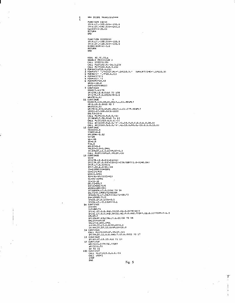
gram implementing these flowcharts is shown in Fig. 5.
Representative computer generated transients for R g
-00, but with finite Ct,
cd’ and rs, are shown in Fig. 6. These curves indicate much the same effects
as shown previously in Fig. 3 except that a turn-on delay is now apparent, and
the turn-off transients, in addition to the delay caused by the stored charge, now
exhibit a slope due to the finite CtO The most general case is shown in Fig. 7,
which includes finite Rg as well as Ct, Cd, and rs.
V. SWITCHING TRANSIENTS WITH THE GENERALIZED
MODEL FOR CONDUCTIVITY MODULATION
Turn-on transients for the circuit of Fig. 2 will be computed with the gener-
alized model for bulk resistance rs as given by Eq. (5). For R -03 and Ct = 0 g
the solution for the junction turn-on current is the same as for Eq. (ll), which
when substituted into Eq.
voltage can be written as
drop :
(6) gives a new value for rs. Then the diode terminal
the sum of the junction voltage and the bulk resistance
(21)
-9-
where 1
Kr = goVs ‘.
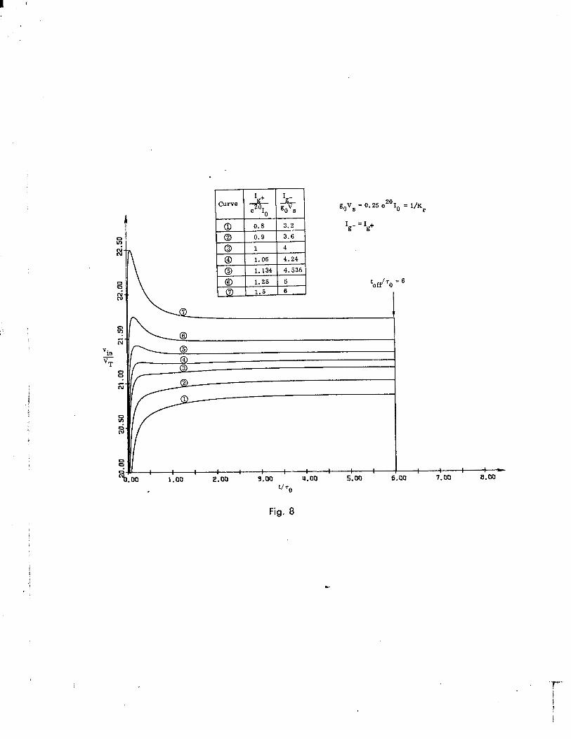
Turn-on transients for Xn = 1 are plotted in Fig. 8 with an expanded scale
for the terminal voltage. Generator currents and other diode parameters are
the same as in Fig. 3(b). Qualitatively the transients of Fig. 8 are similar to
those of Fig. 3(b) which are based upon the simpler version of conductivity modu-
lation. Note that the amount of undershoot is reduced even further from the
small undershoot seen in Fig. 3(b).
VI. SMALL-SIGNAL IMPEDANCE
It is possible to use the model developed in this paper to show that the small-
signal impedance of the junction diode possesses an inductive component at high
forward current levels. This effect has been analyzed’ and measured. 12
The model used in the analysis is the same as shown in Fig. 1 with Ct = 0,
and l/rs = go + ij/VsO Using Eq, (11)
i. ’ dij
in =‘j+‘O dt ’ (22)
The conduction current will be written i. J = I* + i, where I* is the dc part,
and i is the small-signal part. (In the dc case I* = iin. ) Therefore Eq. (22)
becomes ,
i. di in =I*+i+To=& . (23)
Using the complex exponential form for a small-signal sinusoidal i,
di/dt = jwi, and Eq. (23) becomes
i in + juToI*
Ij = 1 f jwTo (24 )
- 10 -

Using Eq. (2) and (8) the diode terminal voltage can now be written in terms of
im: i in + jWTbI* i in
V 1 -I- jWTo
-I- 1 iin f jWToI*
(25)
go ‘v, 1+ jwTo
From this ) the small signal impedance can be shown to be:
A dVin z. =- =
m di. m i in
=I*
Thus the small-signal impedance consists of resistive and reactive portions, . .._.-----
both of which are dependent upon the dc current and upon the signal’ frequency, as .-_I
well as upon the physical parameters of the diode. However, the sign of the re-
actance is not dependent on the frequency. It is seen from Eq. (26) that for nega-
tive I* (0 2 I* > - IO) the junction is reverse-biased and the reactance is always
capacitive.
However, for forward currents the reactance will be inductive if Vs > VT
and
gOvs *T
-fl- J-q (27)
This result, that the reactance may be inductive in certain cases for high
forward currents,, agrees in general with published analytical results on diode
impedance, except at very high frequencies; it is also in good agreement with
measured characteristics of diode impedance at forward currents. 12
- 11 -
t--

VII. SUMMARY
A simple diode model has been presented which includes the effects of con-
ductivity modulation. It has been shown that this model exhibits transient over-
shoot and oscillation, and small-signal inductive impedance at high forward
currents. The model is useful for computer network analysis and synthesis, and
for general qualitative investigations O
- 12 -

LIST OF REFERENCES
1. I. Ladany, “An analysis of inertial inductance in a junction diode,” IRE
Trans. on Electron Devices, ppO 303-310 (October 1960).
2.
3.
4.
5.
6.
7. W. H. Ko, “The forward transient behavior of semiconductor junction
8.
9.
10.
11.
12. Y. Kanai, “On the inductive part in the A. C. characteristics of the semi-
J. F. Gibbons, Semiconductor Electronics, (McGraw-Hill, New York 1966);
p. 291.
J. G. Linvill, Models- of Transistors and Diodes, (McGraw-Hill, New York
1966).
A. F. Malmberg et al. , “NET-l, network analysis program, 7090/94 version,”
Report LA-3119, Los Alamos Scientific Laboratory (Aug. 1964),
D. A. Calahan, Computer Aided Network Design, preliminary edition,
(McGraw-Hill, New York 1968); pp. 253-264.
Y. A. Tkhorik, Transients in Pulsed Semiconductor Diodes, (Israel Pro-
gram for Scientific Translations, Jerusalem, Israel 1968).
diodes, I’ Solid-State Electronics 3, 59-69 (1961),
J. Millman and C. C. Halkias, Electronic Devices and Circuits, (McGraw-
Hill, New York 1967); p- 127.
Millman and Halkias, op. cit. ; p* 139.
Gibbons, op. cit. ; p0 176.
H. L. Armstrong, “On the switching transient in the forward c.onduction of
semiconductor diodes, ” IRE Trans. on Electron Devices, pp. 111-113
(April 1957).
conductor diodes ,” J. Phys. Sot. Japan -2, 718-720 (1955).
- 13 -
‘I-
LIST OF FOOTNOTES
Manuscript received ;
revised .
Work supported by the U. S. Atomic Energy Commission.
Stanford Linear Accelerator Center, Stanford University, Stanford, California 94305.
- *
The resistor Rg can be arbitrarily large, but it cannot be omitted since the
diode junction can support a maximum current of IO in the reverse direction;
thus Rg is necessary to sink current when - Ig < - IO.
- 14 -
1.
2.
3.
4.
5.
6.
7.
8.
LIST OF FIGURES
The diode model.
(a) w (cl (a)
w (a)
(9
The switching circuit to demonstrate forward and reverse transients.
The circuit of (a) incorporating the diode model of Fig, 1.
The current generator waveform, -
Transient response of a diode with R -00, g
Ct = 0, and finite rs, for
different values of normalized generator current. *
Same as 3(a) with expanded vertical scale.
Flowchart of the computer program for computing the transient re-
sponse of the diode.
Flow chart for calculation of step size.
Fortran IV computer program for the flowchart of Fig. 4.
Transient response of diode with R --+a, g
finite Ct, and finite rs, for dif-
ferent values of normalized generator current.
Transient response of diode with finite R g’
finite Ct, and finite rs, for dif-
ferent values of generator current.
Transient response of diode using llexactl’ resistance with Xn =I, Rg-=‘,
and Ct = 0, for different values of normalized generator current.
.
- 15 -

.- II
‘i-7
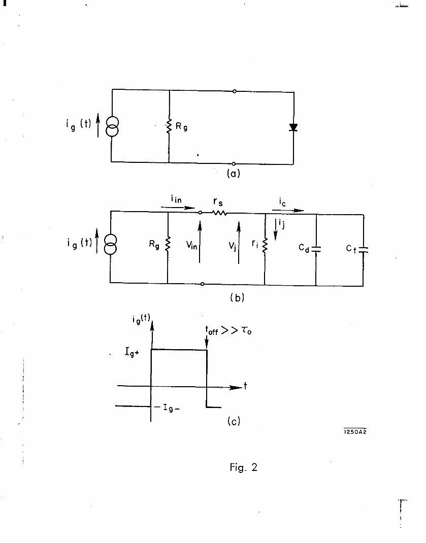
i, (t) 18 _ - Rg Ilt
, (a)
i, 0) t
ij
"j ri Cd Z= cc::
(b)
+,ff > > To
t
i ,tt) 14
1250AZi
Fig. 2

I
50vS t
I ”
I 0 0.1 = 0.4 gOvS 0.25 e2'
0 0.2
I--t 0.8 I g- = Ig+
Q 0.5 2
co 1 4
L 012 8 toff/‘o = 6
Q 15 20
cs
Q
Fig. 3a
‘r- i i

I
I 1.00 2.m
b s.00 U.00 5.00 6.00 7.00 a.00
g v = 0 25 e20 1 OS - 0
Ig- =I + g
t \
Fig. 3b

. .
I INITIALIZE t,v, I
INCREMENT
TIME BY At I
Fig. 4a
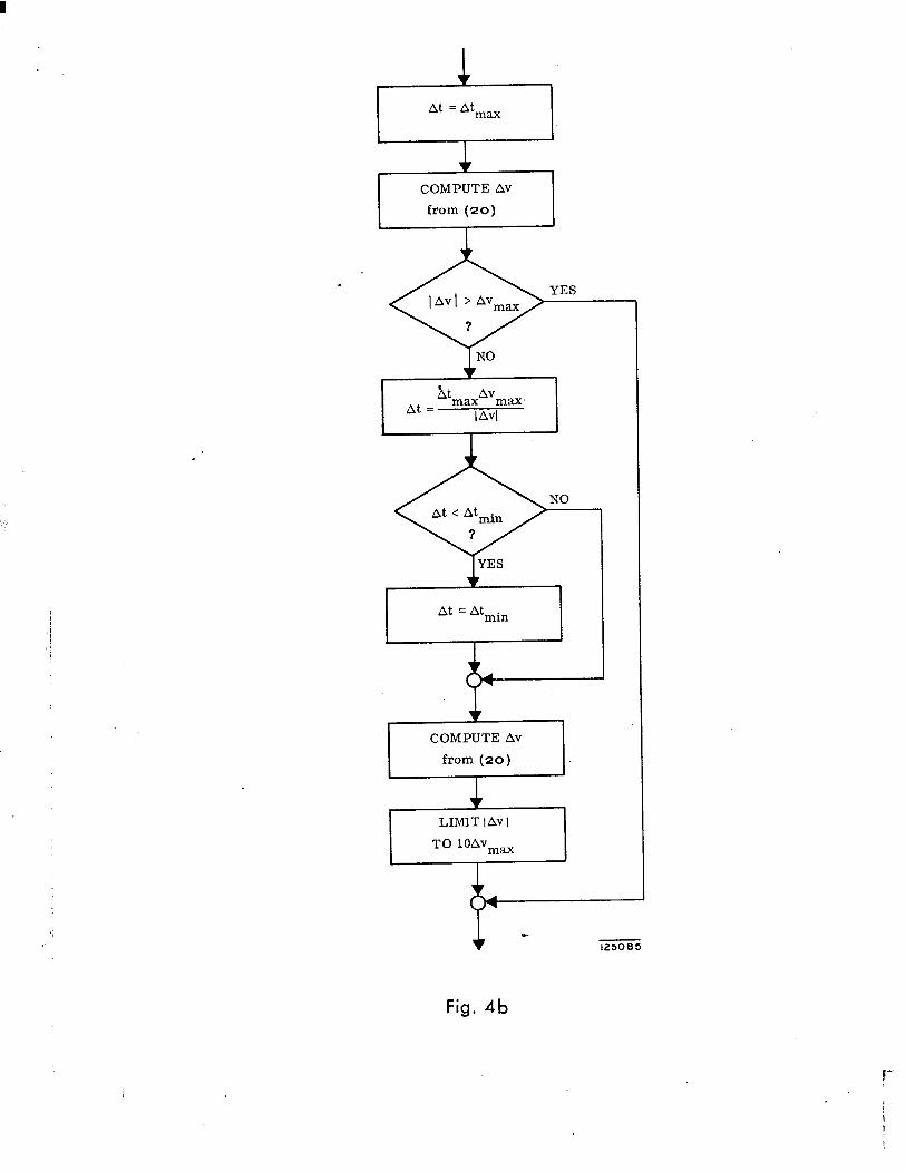
YES
I At At =
I
At = Atmin
COMPUTE Av
from (20)
LIMIT IAv I
TO 10Avmax
I
125085
Fig. 4b
C C
1 2 3 4 5 6
7
11
12
13
*I* DIODE TRANSIENI***
FUNCTION CPIVI IFlV.LT.-lOO.OlV--100.0 IFlV.GT.+140.OlV’tl4o.o CU-EXPIV-20.01 RETURN EN0
FUNCTION DIOOEIVI IFlV.LT.-lOO.OJV--100.0 1FlV.G1.+120.0)V=+120.6 DIODE=EXPIV)-1.0 RETURN END
REAL ID, IC,IGd OOUBLE PRECISLUN V CALL STRTPIl29) CALL PLOTllO.O,-30.0,231 CALL PL0T1l0.0.0.51231 F0R~ATl6F10.4,111 FORMAT, ’ ‘,‘RISETInt-‘.lPEl0.3.’ TURNOFFTlME-‘.lPEIO.31 FORMAT, 1 ‘.?F10.4.111
16
14
15
17
FORMATI’I’I FCRMATI’ ’ I FORflATlF10.kl ARCI--20.0 EXPl.EXPlARGll CONTINUE REA015,6lCTR IFlCTR.LE.O.OlGO TO 100 IFICTR.LT.O.OOllClR=0.0 WRITEl6.41 CON1 INUE I READl5,llG,GN,R1,DELT,L,Cl,NEkPLT IFlG.LE.O.OlGO TO 7 YRITEl6,51 ~R1TEl6r3~G,Gh,Rl,DtLl,L,Cl,CTR,NEWPLT IFlC1.GT.100.O~C1~1E20 DELTZ=lE-6 CALL PLOTll0.0.0.0,+3~ IFlNEWPLT.EQ.OlGO TO 12 CALL PLOTll15.0,0.0,-31 CALL AXIS1l0.O~2.O.‘T’,-1,10.0,0.0,0.0,1.0,2O.Ol CALL AXIS1l0.0,0.0,‘V’,+1,l0.0,90.0,-10.0,5.O,lO.Ol CON1 INUE TRISE-0.0 TTOFF-0.0 XPLOTM--0.02 V--GN VL=-GN IC-0.0 T=O.O XPLOT-0.0 VPLOT-Z.OtO.Z*VL IFIVPLOT.LE.O.OJVPLOT=O.O CALL PLOTllXPLuT,VPLOT,+3J CONTINUE v1=v IFlCTR.LE.O.OIC-CQlV1) IFlCTR.GT.O.OIC-CUlVll4CTR/SQRTl1.O-Vl*0.041 IFlT.LT.6.0lVG=G IFI T.GE.6.0lVG=-GN ID-OIODElVI*EXPl GS-Cl+L*IO GSl-l.O/GS IG-IVG-V)/IGSl+Rll VL-VG-IG*Rl IC-IG-ID OELTl-DELT DV= IC*DELTl/C ABSDV-ABSIOVI IfIABSDV.LT.O.lIGU TO 16 OELll=O.l*OELTl/A6SOV lFlOELT1.LT.OELT2iDELll=DELT2 DV=IC*OELTl/C IFlDV.GT.O.lIOV=0.1 IFlOV.LT.-O.lIOV=-0.1 CONTINUE v=v+clv T-T+DELTl IFlVL.GT.O.O.A~O.TRlSE.EU.O.OlTRISE=l IFIVL.LT.O.O.AND.TRISE.NE.O.O.ANO.TTOFF.EQ.O.OITTOFF~T-6.0 ~PLOT=T IFIXPLOT-XPLOTH.LT.O.01160 TO 15 XPLOTM-XPLOT vPL01=2.0+0.2*VL IFlVPLOT.LT.O.OlVPLOT=O.O IFlVPLOT.GT.10.01VPLU~=lO.O CONTINUE CALL PLOTlIXPLOT,VPLOT,+ZI IFIVPLOT.LE.O.O.ANO.T.GT.6.OlGO TO 17 CONTINUE IFIXPLOT.LE.lO.iGU IO 13 CONTINUE YRITEI~,ZITRISE,TTOFF WRlTEl6,51 GO TO 11
100 CONTINUE CALL PLOTll15.0,0.01-31 CALL ENOPl STOP EN0
Fig. 5

20 gOVs=0.25e IO
V. = 25 VT
m = 0.5
COVT 7= 0.01
t oloe
tofdro = 6
Ig- =I + g
I
Fig. 6

‘1 . .
:urve x &
e201 0
gOvS
0 0.5 2
$ 2 1 4
a 8 5 20
0 0.5 2
T-r
1
$ 2 4
a
8 5 20
goVs = 0.25 e 20
1.
V. = 25 V T
m=0.5
‘OVT --zjyj= 0.01
T oloe
I g-
= Ig+
Fig. 7
N
. --
B c1)
b 0
c 2
L b 0 ul
-0
0 ml
b 0 4 b 0 .w.-
0 0
t
_ .,“
--“_
. -I