a-si tft lcd single chip driver 320rgbx240 resolution · pdf file320rgbx240 resolution and...
TRANSCRIPT

ILI9342
a-Si TFT LCD Single Chip Driver 320RGBx240 Resolution and 262K color
Specification Preliminary
Version: V007 Document No.: ILI9342_DS_V007.pdf
ILI TECHNOLOGY CORP. 8F, No. 38, Taiyuan St., Jhubei City, Hsinchu Country 302 Taiwan R.O.C. Tel.886-3-5600099; Fax.886-3-5670585 http://www.ilitek.com

a-Si TFT LCD Single Chip Driver
320RGBx240 Resolution and 262K color ILI9342
The information contained herein is the exclusive property of ILI Technology Corp. and shall not be distributed, reproduced, or disclosed in whole or in part without prior written permission of ILI Technology Corp. Page 2 of 216
Table of Contents
Section Page
1. Introduction.................................................................................................................................................... 7
2. Features ........................................................................................................................................................ 7
3. Block Diagram............................................................................................................................................... 9
4. Block Function Description.......................................................................................................................... 10
5. Pin Description ............................................................................................................................................ 12
6. Pad Arrangement and Coordination............................................................................................................ 16
6.1. PAD Coordinate ............................................................................................................................. 17
6.2. Bump Arrangement ........................................................................................................................ 26
7. Function Description ................................................................................................................................... 27
7.1. MPU interfaces............................................................................................................................... 27
7.1.1. MPU interface selection....................................................................................................... 27
7.1.2. 8080-Series Parallel Interface ............................................................................................. 28
7.1.3. Write Cycle Sequence ......................................................................................................... 29
7.1.4. Read Cycle Sequence......................................................................................................... 30
7.1.5. 6800-Series Parallel Interface ............................................................................................. 31
7.1.6. Write Cycle Sequence ......................................................................................................... 33
7.1.7. Read Cycle Sequence......................................................................................................... 35
7.1.8. Serial Interface .................................................................................................................... 37
7.1.9. Write Cycle Sequence ......................................................................................................... 37
7.1.10. Read Cycle Sequence......................................................................................................... 39
7.1.11. Data Transfer Break and Recovery ..................................................................................... 42
7.1.12. Data Transfer Pause............................................................................................................ 44
7.1.13. Serial Interface Pause (3_wire) ........................................................................................... 45
7.1.14. Parallel Interface Pause ...................................................................................................... 45
7.1.15. Data Transfer Mode............................................................................................................. 46
7.1.16. Data Transfer Method 1....................................................................................................... 46
7.1.17. Data Transfer Method 2....................................................................................................... 46
7.2. RGB Interface ................................................................................................................................ 47
7.2.1. RGB Interface Selection...................................................................................................... 47
7.2.2. RGB Interface Timing .......................................................................................................... 51
7.3. VSYNC Interface............................................................................................................................ 53
7.4. Color Depth Conversion Look-Up Table ........................................................................................ 57
7.5. Display Data RAM (DDRAM) ......................................................................................................... 61
7.6. Display Data Format ...................................................................................................................... 62
7.6.1. 3-line Serial Interface........................................................................................................... 62
7.6.2. 4-line Serial Interface........................................................................................................... 64
7.6.3. 8-bit Parallel MPU Interface ................................................................................................ 66
a-Si TFT LCD Single Chip Driver
320RGBx240 Resolution and 262K color ILI9342
The information contained herein is the exclusive property of ILI Technology Corp. and shall not be distributed, reproduced, or disclosed in whole or in part without prior written permission of ILI Technology Corp. Page 3 of 216
7.6.3.1. 8-bit Data Bus for 12-bit/pixel (RGB 4-4-4 bits input), 4K-color .......................................... 67
7.6.3.2. 8-bit Data Bus for 16-bit/pixel (RGB 5-6-5 bits input), 65K-color ........................................ 68
7.6.3.3. 8-bit Data Bus for 18-bit/pixel (RGB 6-6-6 bits input), 262K-color ...................................... 69
7.6.4. 9-bit Parallel MPU Interface ................................................................................................ 70
7.6.4.1. 9-bit Data Bus for 18-bit/pixel (RGB 6-6-6 bits input), 262K-color ...................................... 71
7.6.5. 16-bit Parallel MPU Interface .............................................................................................. 72
7.6.5.1. 16-bit Data Bus for 12-bit/pixel (RGB 4-4-4 bits input), 4K-color ........................................ 73
7.6.5.2. 16-bit Data Bus for 16-bit/pixel (RGB 5-6-5 bits input), 65K-color ...................................... 74
7.6.5.3. 16-bit Data Bus for 18-bit/pixel (RGB 6-6-6 bits input), 262K-color .................................... 75
7.6.6. 18-bit Parallel MPU Interface .............................................................................................. 76
7.6.6.1. 18-bit Data Bus for 18-bit/pixel (RGB 6-6-6 bits input), 262K-color .................................... 77
7.6.7. 6-bit Parallel RGB Interface................................................................................................. 78
7.6.8. 16-bit Parallel RGB Interface............................................................................................... 80
7.6.9. 18-bit Parallel RGB Interface............................................................................................... 81
8. Command.................................................................................................................................................... 82
8.1. Command List ................................................................................................................................ 82
8.2. Description of Regulative Command Set ....................................................................................... 87
8.2.1. NOP (00h)............................................................................................................................ 87
8.2.2. Software Reset (01h)........................................................................................................... 88
8.2.3. Read display identification information (04h) ...................................................................... 89
8.2.4. Read Display Status (09h)................................................................................................... 90
8.2.5. Read Display Power Mode (0Ah) ........................................................................................ 92
8.2.6. Read Display MADCTL (0Bh).............................................................................................. 93
8.2.7. Read Display Pixel Format (0Ch)........................................................................................ 94
8.2.8. Read Display Image Format (0Dh)...................................................................................... 95
8.2.9. Read Display Signal Mode (0Eh) ........................................................................................ 96
8.2.10. Read Display Self-Diagnostic Result (0Fh) ......................................................................... 97
8.2.11. Enter Sleep Mode (10h) ...................................................................................................... 98
8.2.12. Sleep Out (11h) ................................................................................................................... 99
8.2.13. Partial Mode ON (12h)....................................................................................................... 101
8.2.14. Normal Display Mode ON (13h) ........................................................................................ 102
8.2.15. Display Inversion OFF (20h).............................................................................................. 103
8.2.16. Display Inversion ON (21h) ............................................................................................... 104
8.2.17. Gamma Set (26h) .............................................................................................................. 105
8.2.18. Display OFF (28h) ............................................................................................................. 106
8.2.19. Display ON (29h) ............................................................................................................... 107
8.2.20. Column Address Set (2Ah)................................................................................................ 108
8.2.21. Page Address Set (2Bh) .................................................................................................... 110
8.2.22. Memory Write (2Ch) .......................................................................................................... 112
a-Si TFT LCD Single Chip Driver
320RGBx240 Resolution and 262K color ILI9342
The information contained herein is the exclusive property of ILI Technology Corp. and shall not be distributed, reproduced, or disclosed in whole or in part without prior written permission of ILI Technology Corp. Page 4 of 216
8.2.23. Color Set (2Dh).................................................................................................................. 113
8.2.24. Memory Read (2Eh) .......................................................................................................... 114
8.2.25. Partial Area (30h)............................................................................................................... 116
8.2.26. Vertical Scrolling Definition (33h) ...................................................................................... 118
8.2.27. Tearing Effect Line OFF (34h) ........................................................................................... 122
8.2.28. Tearing Effect Line ON (35h) ............................................................................................. 123
8.2.29. Memory Access Control (36h) ........................................................................................... 125
8.2.30. Vertical Scrolling Start Address (37h) ................................................................................ 127
8.2.31. Idle Mode OFF (38h) ......................................................................................................... 129
8.2.32. Idle Mode ON (39h) ........................................................................................................... 130
8.2.33. COLMOD: Pixel Format Set (3Ah) .................................................................................... 132
8.2.34. Write Memory Continue (3Ch)........................................................................................... 133
8.2.35. Read Memory Continue (3Eh)........................................................................................... 135
8.2.36. Set Tear Scan line (44h) .................................................................................................... 137
8.2.37. Get Scan line (45h)............................................................................................................ 138
8.2.38. Read ID1 (DAh) ................................................................................................................. 139
8.2.39. Read ID2 (DBh) ................................................................................................................. 140
8.2.40. Read ID3 (DCh)................................................................................................................. 141
8.3. Description of Extended Command set ....................................................................................... 142
8.3.1. RGB Interface Signal Control (B0h) .................................................................................. 142
8.3.2. Display Waveform Cycle 1 (In Normal Mode/Full Colors) (B1h) ....................................... 143
8.3.3. Display Waveform Cycle 2 (In Idle Mode/8 colors) (B2h).................................................. 144
8.3.4. Display Waveform Cycle (In Partial Mode/Full Colors) (B3h) ........................................... 145
8.3.5. Display Inversion Control (B4h)......................................................................................... 146
8.3.6. Blanking Porch Control (B5h)............................................................................................ 148
8.3.7. Display Function Control (B6h) ......................................................................................... 150
8.3.8. Entry Mode Set (B7h) ........................................................................................................ 154
8.3.9. Oscillator Control (B8h) ..................................................................................................... 155
8.3.10. Set EXTC (B9h)................................................................................................................. 156
8.3.11. Power Control 1 (C0h)....................................................................................................... 157
8.3.12. Power Control 2 (C1h)....................................................................................................... 159
8.3.13. Power Control 3 (For Normal Mode) (C2h) ....................................................................... 161
8.3.14. Power Control 4 (For Idle Mode) (C3h) ............................................................................. 162
8.3.15. Power Control 5 (For Partial Mode) (C4h)......................................................................... 163
8.3.16. VCOM Control 1(C5h) ....................................................................................................... 164
8.3.17. VCOM Control 2(C7h) ....................................................................................................... 166
8.3.18. NV Memory Write (D0h) .................................................................................................... 168
8.3.19. NV Memory Protection Key (D1h) ..................................................................................... 169
8.3.20. NV Memory Status Read (D2h)......................................................................................... 170

a-Si TFT LCD Single Chip Driver
320RGBx240 Resolution and 262K color ILI9342
The information contained herein is the exclusive property of ILI Technology Corp. and shall not be distributed, reproduced, or disclosed in whole or in part without prior written permission of ILI Technology Corp. Page 5 of 216
8.3.21. Read ID4 (D3h) ................................................................................................................. 171
8.3.22. Positive Gamma Correction (E0h)..................................................................................... 172
8.3.23. Negative Gamma Correction (E1h) ................................................................................... 173
8.3.24. Digital Gamma Control 1 (E2h) ......................................................................................... 174
8.3.25. Digital Gamma Control 2(E3h) .......................................................................................... 175
8.3.26. Interface Control (F6h) ...................................................................................................... 176
8.3.27. Get GPIO0~7 Status (F7h) ................................................................................................ 179
8.3.28. Set GPIO0~7 Status (F8h) ................................................................................................ 180
9. Display Data RAM..................................................................................................................................... 181
9.1. Configuration................................................................................................................................ 181
9.2. Memory to Display Address Mapping .......................................................................................... 182
9.2.1. Normal Display ON or Partial Mode ON, Vertical Scroll Mode OFF ................................. 182
9.2.2. Vertical Scroll Mode........................................................................................................... 183
9.2.3. Vertical Scroll Example...................................................................................................... 184
9.2.4. Case1: TFA+VSA+BFA < 240 ........................................................................................... 184
9.2.5. Case2: TFA+VSA+BFA = 240 (Rolling Scrolling) .............................................................. 184
9.3. MPU to memory write/read direction............................................................................................ 186
10. Tearing Effect Output ................................................................................................................................ 189
10.1. Tearing Effect Line Modes............................................................................................................ 189
10.2. Tearing Effect Line Timings .......................................................................................................... 190
11. Sleep Out – Command and Self-Diagnostic Functions of the Display Module......................................... 191
11.1. Register loading Detection........................................................................................................... 191
11.2. Functionality Detection................................................................................................................. 192
12. Power ON/OFF Sequence ........................................................................................................................ 193
12.1. Case 1 – RESX line is held High or Unstable by Host at Power ON........................................... 193
12.2. Case 2 – RESX line is held Low by Host at Power ON ............................................................... 194
12.3. Uncontrolled Power Off ................................................................................................................ 195
13. Power Level Definition .............................................................................................................................. 196
13.1. Power Levels................................................................................................................................ 196
13.2. Power Flow Chart......................................................................................................................... 197
14. Gamma Curves Selection ......................................................................................................................... 198
14.1. Gamma Default Values (for NW type LC) .................................................................................... 198
14.2. Gamma Curves ............................................................................................................................ 199
14.2.1. Gamma Curve 1 (GC0), applies the function y=x2.2 .......................................................... 199
14.2.2. Gamma Curve 2 (GC1), applies the function y=x1.8 .......................................................... 199
14.2.3. Gamma Curve 3 (GC2), applies the function y=x2.5 .......................................................... 199
14.2.4. Gamma Curve 4 (GC3), applies the function y=x1.0 .......................................................... 199
15. Reset ......................................................................................................................................................... 200
15.1. Registers ...................................................................................................................................... 200
a-Si TFT LCD Single Chip Driver
320RGBx240 Resolution and 262K color ILI9342
The information contained herein is the exclusive property of ILI Technology Corp. and shall not be distributed, reproduced, or disclosed in whole or in part without prior written permission of ILI Technology Corp. Page 6 of 216
15.2. Output Pins, I/O Pins.................................................................................................................... 201
15.3. Input Pins ..................................................................................................................................... 201
15.4. Reset Timing ................................................................................................................................ 202
16. NV Memory Programming Flow................................................................................................................ 203
17. Deep Standby Mode Setting ..................................................................................................................... 204
18. Electrical Characteristics........................................................................................................................... 205
18.1. Absolute Maximum Ratings ......................................................................................................... 205
18.2. DC Characteristics ....................................................................................................................... 206
18.2.1. General DC Characteristics............................................................................................... 206
18.3. AC Characteristics ....................................................................................................................... 207
18.3.1. Display Parallel 18/16/9/8-bit Interface Timing Characteristics (8080-system)................. 207
18.3.2. Display Parallel 18/16/9/8-bit Interface Timing Characteristics (6800-system)................. 209
18.3.3. Fixed E Mode .................................................................................................................... 209
18.3.4. Clocked E Mode ................................................................................................................ 210
18.3.5. Display Serial Interface Timing Characteristics (3-line SPI system) ................................. 211
18.3.6. Display Serial Interface Timing Characteristics (4-line SPI system) ................................. 212
18.3.7. Parallel RGB Interface Timing Characteristics .................................................................. 213
19. Application Circuit ..................................................................................................................................... 214
20. Revision History ........................................................................................................................................ 216
a-Si TFT LCD Single Chip Driver
320RGBx240 Resolution and 262K color ILI9342
The information contained herein is the exclusive property of ILI Technology Corp. and shall not be distributed, reproduced, or disclosed in whole or in part without prior written permission of ILI Technology Corp. Page 7 of 216
1. Introduction
ILI9342 is a 262,144-color single-chip SOC driver for a-TFT liquid crystal display with resolution of 320RGBx240
dots, comprising a 960-channel source driver, a 240-channel gate driver, 172,800 bytes GRAM for graphic
display data of 320RGBx240 dots, and power supply circuit.
ILI9342 supports parallel 8-/9-/16-/18-bit data bus MPU interface, 6-/16-/18-bit data bus RGB interface and
3-/4-line serial peripheral interface (SPI). The moving picture area can be specified in internal GRAM by window
address function. The specified window area can be updated selectively, so that moving picture can be
displayed simultaneously independent of still picture area.
ILI9342 can operate with 1.65V ~ 3.6V I/O interface voltage and an incorporated voltage follower circuit to
generate voltage levels for driving an LCD. ILI9342 supports full color, 8-color display mode and sleep mode for
precise power control by software and these features make the ILI9342 an ideal LCD driver for medium or small
size portable products such as digital cellular phones, smart phone, MP3 and PMP where long battery life is a
major concern.
2. Features
Display resolution: [320xRGB](H) x 240(V)
Output:
960 source outputs
240 gate outputs
Common electrode output (VCOM)
a-TFT LCD driver with on-chip full display RAM: 172,800 bytes
System Interface
8-bits, 9-bits, 16-bits, 18-bits interface with 6800/8080-series MPU
6-bits, 16-bits, 18-bits RGB interface with graphic controller
3-line / 4-line serial interface
Display mode:
Full color mode (Idle mode OFF): 262K-color (selectable color depth mode by software)
Reduce color mode (Idle mode ON): 8-color
Power saving mode:
Sleep mode
Deep standby mode
On chip functions:
VCOM generator and adjustment
Timing generator
Oscillator
DC/DC converter
Line/frame inversion
4 preset selectable gamma curves
MTP (3 times):
8-bits for ID1, ID2, ID3
7-bits for VCOM adjustment

a-Si TFT LCD Single Chip Driver
320RGBx240 Resolution and 262K color ILI9342
The information contained herein is the exclusive property of ILI Technology Corp. and shall not be distributed, reproduced, or disclosed in whole or in part without prior written permission of ILI Technology Corp. Page 8 of 216
Low -power consumption architecture
Low operating power supplies:
IOVCC = 1.65V ~ 3.3V (logic)
VCI = 2.4V ~ 4.8V (analog)
LCD Voltage drive:
Source/VCOM power supply voltage
DDVDH - GND = 4.5V ~ 6.0V
VCL - GND = -2.0V ~ -3.0V
Gate driver output voltage
VGH - GND = 10.0V ~ 20.0V
VGL - GND = -5.0V ~ -15.0V
VGH - VGL ≦ 32V
VCOM driver output voltage
VCOMH = 3.0V ~ (DDVDH – 0.5)V
VCOML = (VCL+0.5)V ~ 0V
VCOMH - VCOML ≦ 6.0V
Operate temperature range: -40℃ to 85℃
a-Si TFT LCD storage capacitor : Cst on Common structure only

a-Si TFT LCD Single Chip Driver
320RGBx240 Resolution and 262K color ILI9342
The information contained herein is the exclusive property of ILI Technology Corp. and shall not be distributed, reproduced, or disclosed in whole or in part without prior written permission of ILI Technology Corp. Page 9 of 216
3. Block Diagram
8 / 9 / 16 / 18-bit MP U I / F
3 /4 line S erial I/F
8 / 16 / 18 -bit RGB I / F
CSX WRX
RDX
D / CX
D [ 17 :0]
SDA
VSYNC HSYNC
DOTCLK
RESX
IM[ 3:0]
DUMMY R 3,4
IOVCC
RegulatorDGND
RC - OSC . Timing Controller
Charge -pump Power Circuit
VREG1OUT
C 11P
VCI
C 1 1 N
D D VD H
C12P
C 12N
VCL
C22P
C22N
VGH
VGL
VCOM Generator
VCOM
IndexRegister
(IR)
Control Register
(CR)
18
8
GraphicsOperation
18
ReadLatch
18
18
WriteLatch
Graphics RAM(GRAM)
1818
Address Counter
(AC)
LCD Source Driver
Grayscale Reference
Voltage
V 63 ~ V0
S960 ~ S1
LCD Gate Driver
G240 ~ G1
AGND
VCORE
C31P
C31N
C 21P
C 2 1 N
DE
DUMMYR 1, 2
TE
18
4
VGS
V C OM L
VC OM H
TEST_EN
TEST0~ 8
DUMMY
VCI
GPIO0~ 7
TEST_OSC
a-Si TFT LCD Single Chip Driver
320RGBx240 Resolution and 262K color ILI9342
The information contained herein is the exclusive property of ILI Technology Corp. and shall not be distributed, reproduced, or disclosed in whole or in part without prior written permission of ILI Technology Corp. Page 10 of 216
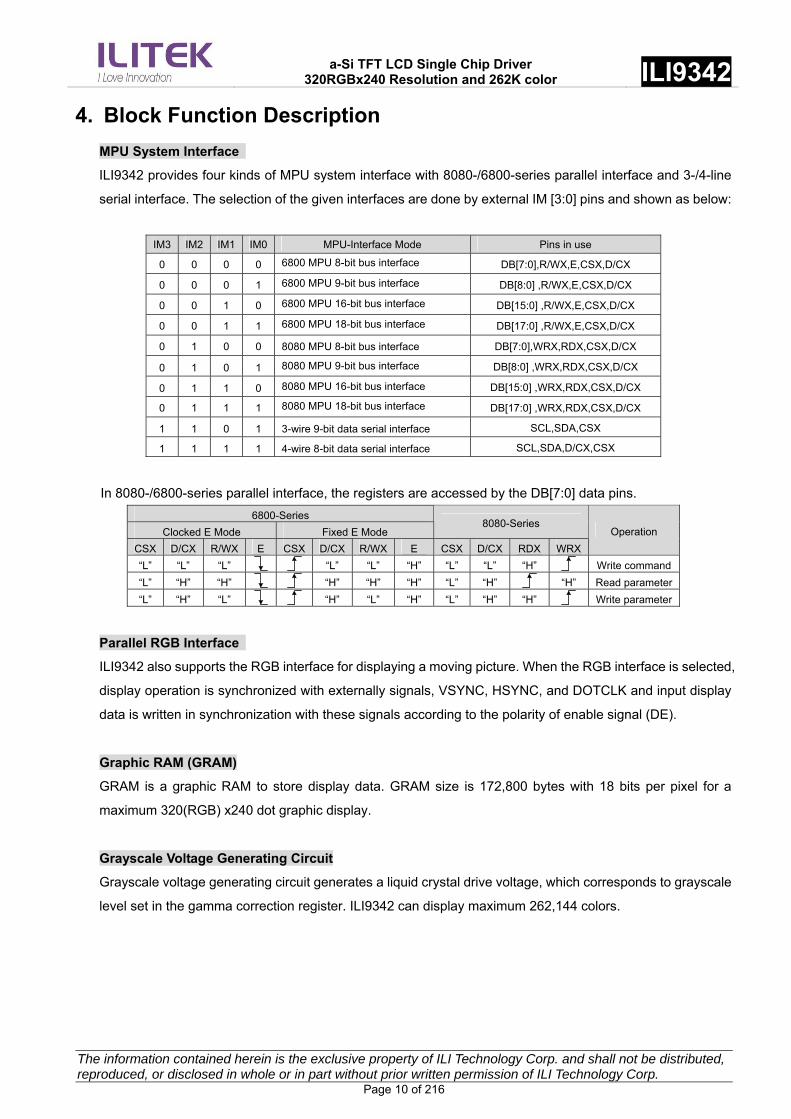
4. Block Function Description
MPU System Interface
ILI9342 provides four kinds of MPU system interface with 8080-/6800-series parallel interface and 3-/4-line
serial interface. The selection of the given interfaces are done by external IM [3:0] pins and shown as below:
IM3 IM2 IM1 IM0 MPU-Interface Mode Pins in use
0 0 0 0 6800 MPU 8-bit bus interface DB[7:0],R/WX,E,CSX,D/CX
0 0 0 1 6800 MPU 9-bit bus interface DB[8:0] ,R/WX,E,CSX,D/CX
0 0 1 0 6800 MPU 16-bit bus interface DB[15:0] ,R/WX,E,CSX,D/CX
0 0 1 1 6800 MPU 18-bit bus interface DB[17:0] ,R/WX,E,CSX,D/CX
0 1 0 0 8080 MPU 8-bit bus interface DB[7:0],WRX,RDX,CSX,D/CX
0 1 0 1 8080 MPU 9-bit bus interface DB[8:0] ,WRX,RDX,CSX,D/CX
0 1 1 0 8080 MPU 16-bit bus interface DB[15:0] ,WRX,RDX,CSX,D/CX
0 1 1 1 8080 MPU 18-bit bus interface DB[17:0] ,WRX,RDX,CSX,D/CX
1 1 0 1 3-wire 9-bit data serial interface SCL,SDA,CSX
1 1 1 1 4-wire 8-bit data serial interface SCL,SDA,D/CX,CSX
In 8080-/6800-series parallel interface, the registers are accessed by the DB[7:0] data pins.
6800-Series
Clocked E Mode Fixed E Mode 8080-Series
CSX D/CX R/WX E CSX D/CX R/WX E CSX D/CX RDX WRX
Operation
“L” “L” “L” “L” “L” “H” “L” “L” “H” Write command
“L” “H” “H” “H” “H” “H” “L” “H” “H” Read parameter
“L” “H” “L” “H” “L” “H” “L” “H” “H” Write parameter
Parallel RGB Interface
ILI9342 also supports the RGB interface for displaying a moving picture. When the RGB interface is selected,
display operation is synchronized with externally signals, VSYNC, HSYNC, and DOTCLK and input display
data is written in synchronization with these signals according to the polarity of enable signal (DE).
Graphic RAM (GRAM)
GRAM is a graphic RAM to store display data. GRAM size is 172,800 bytes with 18 bits per pixel for a
maximum 320(RGB) x240 dot graphic display.
Grayscale Voltage Generating Circuit
Grayscale voltage generating circuit generates a liquid crystal drive voltage, which corresponds to grayscale
level set in the gamma correction register. ILI9342 can display maximum 262,144 colors.

a-Si TFT LCD Single Chip Driver
320RGBx240 Resolution and 262K color ILI9342
The information contained herein is the exclusive property of ILI Technology Corp. and shall not be distributed, reproduced, or disclosed in whole or in part without prior written permission of ILI Technology Corp. Page 11 of 216
Power Supply Circuit
The LCD drive power supply circuit generates the voltage levels as VREG1OUT, VGH, VGL and VCOM for
driving TFT LCD panel.
Timing controller
The timing controller generates all the timing signals for display and GRAM access.
Oscillator
ILI9342 incorporates RC oscillator circuit and output a stable output frequency for operation.
Panel Driver Circuit
Liquid crystal display driver circuit consists of 960-output source driver (S1~S960), 240-output gate driver
(G1~G240), and VCOM signal.

a-Si TFT LCD Single Chip Driver
320RGBx240 Resolution and 262K color ILI9342
The information contained herein is the exclusive property of ILI Technology Corp. and shall not be distributed, reproduced, or disclosed in whole or in part without prior written permission of ILI Technology Corp. Page 12 of 216
5. Pin Description
Bus Interface Pins Pin Name I/O Type Descriptions
IM[3:0] I MPU
(IOVCC/DGND)
- Select the MPU interface mode IM3 IM2 IM1 IM0 MPU-Interface Mode DB Pin in use
0 0 0 0 6800 8-bit bus interface DB[7:0]
0 0 0 1 6800 9-bit bus interface DB[8:0]
0 0 1 0 6800 16-bit bus interface DB[15:0]
0 0 1 1 6800 18-bit bus interface DB[17:0]
0 1 0 0 8080 8-bit bus interface DB[7:0]
0 1 0 1 8080 9-bit bus interface DB[8:0]
0 1 1 0 8080 16-bit bus interface DB[15:0]
0 1 1 1 8080 18-bit bus interface DB[17:0]
1 1 0 1 3-line SPI SDA
1 1 1 1 4-line SPI SDA
(Other setting is inhibited)
MPU Parallel interface bus and serial interface select
Fix this pin at IOVCC or DGND.
RESX I MPU
(IOVCC/DGND)
This signal will reset the device and must be applied to properly
initialize the chip.
Signal is active low.
CSX(CSX1) I MPU
(IOVCC/DGND)
Chip select input pin (“Low” enable). This pin can be permanently fixed “Low” in MPU interface mode only. CSX and CSX1 are connected internally winthin IC.
Note : 1,2.
D/CX(D/CX_SCL1) (SCL)
I MPU
(IOVCC/DGND)
This pin is used to select “Data or Command” in the parallel
interface or 4-wire 8-bit serial data interface.
When DCX = ’1’, data is selected.
When DCX = ’0’, command is selected.
This pin is used serial interface clock in 3-wire 9-bit / 4-wire 8-bit
serial data interface.
D/CX and D/CX_SCL1 are connected internally winthin IC.
Fix to IOVCC or DGND level when not in use.
RDX (E) I MPU
(IOVCC/DGND)
- 8080 system (RDX): Serves as a read signal and MPU read data at the rising edge.
- 6800 system (E): Serves as a enable/disable signal for
read/write operation.
Fix to IOVCC or DGND level when not in use.
WRX (R/WX) (D/CX)
I MPU
(IOVCC/DGND)
- 8080 system (WRX): Serves as a write signal and writes data at the rising edge.
- 6800 system (R/WX): Serves as a write/read control signal. - 4-line system (D/CX): Serves as command or parameter select.
Fix to IOVCC or DGND level when not in use.
DB[17:0] I/O MPU
(IOVCC/DGND)
18-bit parallel bi-directional data bus for MPU system and RGB interface mode
Fix to DGND level when not in use

a-Si TFT LCD Single Chip Driver
320RGBx240 Resolution and 262K color ILI9342
The information contained herein is the exclusive property of ILI Technology Corp. and shall not be distributed, reproduced, or disclosed in whole or in part without prior written permission of ILI Technology Corp. Page 13 of 216
SDA I/O MPU
(IOVCC/DGND)
Serial data input / output and applied on the rising edge of the
SCL signal.
If not used, fix this pin at IOVCC or DGND.
TE O MPU
(IOVCC/DGND)
Tearing effect output pin to synchronize MPU to frame writing,
activated by S/W command. When this pin is not activated, this
pin is low.
If not used, open this pin.
DOTCLK I MPU
(IOVCC/DGND)Dot clock signal for RGB interface operation. Fix to IOVCC or DGND level when not in use.
VSYNC I MPU
(IOVCC/DGND)Frame synchronizing signal for RGB interface operation. Fix to IOVCC or DGND level when not in use.
HSYNC I MPU
(IOVCC/DGND)Line synchronizing signal for RGB interface operation. Fix to IOVCC or DGND level when not in use.
DE I MPU
(IOVCC/DGND)Data enable signal for RGB interface operation. Fix to IOVCC or DGND level when not in use.
LCD Driving Signals Pin Name I/O Type Descriptions
S960~S1 O Source Source output signals.. Leave the pin to open when not in use.
G240~G1 O Gate Gate output signals. Leave the pin to open when not in use.
VCOM O TFT common
electrode
Power supply pad for the TFT- display counter electrode.
Charge recycling method is used with VCI and AGND voltage.
Connect this pad to the TFT-display counter electrode. VCOMH O - - The high level of VCOM AC voltage. VCOML O - - The low level of VCOM AC voltage.
Charge-pump and Regulator Circuit Pin Name I/O Type Descriptions
DDVDH O Stabilizing capacitor
Output voltage of 1st step up circuit (2 x VCI1). Input voltage to 2nd step up circuit. Generated power output pad for source driver block. Connect this pad to the capacitor for stabilization. Note : 3.
VGH O Stabilizing capacitor
Power supply for the gate driver. Adjust the VGH level with the BT[2:0] bits. Connect this pad with a stabilizing capacitor.
VGL O Stabilizing capacitor
Power supply for the gate driver. Adjust the VGL level with the BT[2:0] bits. Connect this pad with a stabilizing capacitor.
VCL O Stabilizing capacitor
Power supply for VCOML. VCL = 0~ - VCI1 Connect this pad with a stabilizing capacitor.
C11P, C11N C12P, C12N
P Step-up capacitor
Connect the charge-pumping capacitor for generating DDVDH level.
C21P, C21N C22P, C22N
P Step-up capacitor
Connect the charge-pumping capacitor for generating VGH, VGL level.
C31P, C31N P Step-up capacitor
Connect the charge-pumping capacitor for generating VCL level.
VREG1OUT O - Reference voltage for grayscale voltage generator.
Internal register can be used to adjust the voltage.
VGS I Power supply
- Reference voltage input for grayscale voltage generator. - Connect an external resistor or to system ground.
Power Pads Pin Name I/O Type Descriptions

a-Si TFT LCD Single Chip Driver
320RGBx240 Resolution and 262K color ILI9342
The information contained herein is the exclusive property of ILI Technology Corp. and shall not be distributed, reproduced, or disclosed in whole or in part without prior written permission of ILI Technology Corp. Page 14 of 216
IOVCC I Power supply
Power supply for interface logic circuits (1.65 ~ 3.6 V)
VCI I Power supply
Power supply for analog circuit blocks (2.4 ~ 3.6 V)
VCORE O Digital Power
Regulated Low voltage level for interface circuits. Don’t apply any
external power to this pad.
Connect a capacitor for stabilization.
DGND I Digital Ground System ground level for logic blocks
AGND I Analog GroundSystem ground level for analog circuit blocks
Connect to DGND on the FPC to prevent noise.
VPP I Power supply
Power supply pin used in NV memory write mode and operated
at 7.0V
Leave the pin to open when not in use.
Test Pads Pin Name I/O Type Descriptions TEST_EN
TEST_OSC I DGND
TEST pin input(internal pull low), Connect to GND when not used
TESTO1~2 O Open TEST pin output, Leave it open when not used
TEST0~8 I DGND TEST pin(internal pull low), Connect to GND when not used
DUMMYR1 DUMMYR2 DUMMYR3 DUMMYR4
- Open
Contact resistance measurement pad. In normal operation, leave this unconnected. These pads are at DGND level.When measuring an ohm resistance of the contact, do not apply any power.
DUMMY - Open Input pads used only for test purpose at IC-side. During normal operation, leave these pads open.
GPIO0~7 I/O - Standard input/output pin As for GPIO0~7 to terminal, setting of an input and output direction is possible
Note : 1. If CSX is connected to DGND in Parallel interface mode, there will be no abnormal visible effect to the
display module. Also there will be no restriction on using the Parallel Read/Write protocols, Power
On/Off Sequences or other functions. Furthermore there will be no influence to the Power Consumption
of the display module.
2. When CSX='1', there is no influence to the parallel and serial interface.
3. VCI1 is an internal reference voltage generated between VCI and AGND. Reference input voltage for
1st and 3rd step up circuit.

a-Si TFT LCD Single Chip Driver
320RGBx240 Resolution and 262K color ILI9342
The information contained herein is the exclusive property of ILI Technology Corp. and shall not be distributed, reproduced, or disclosed in whole or in part without prior written permission of ILI Technology Corp. Page 15 of 216
Liquid crystal power supply specifications Table
No. Item Description 1 TFT Source Driver 960 pins (320 x RGB) 2 TFT Gate Driver 240 pins 3 TFT Display’s Capacitor Structure Cst structure only (Cs on Common)
S1 ~ S960 V0 ~ V63 grayscales G1 ~ G240 VGH - VGL 4 Liquid Crystal Drive Output
VCOM VCOMH - VCOML: Amplitude = electronic volumes IOVCC 1.65V ~ 3.30V
5 Input Voltage VCI 2.30V ~ 4.80V
DDVDH 4.5V ~ 6.0V VGH 10.0V ~ 20.0V VGL -5.0V ~ -15.0V VCL -1.9V ~ -3.0V
6 Liquid Crystal Drive Voltages
VGH - VGL Max. 32.0V DDVDH VCI1 x2, x3
VGH VCI1 x4, x5, x6, x7, x9 VGL VCI1 x-3, x-4, x-5, x-6, x-7
7 Internal Step-up Circuits
VCL VCI1 x-1
a-Si TFT LCD Single Chip Driver
320RGBx240 Resolution and 262K color ILI9342
The information contained herein is the exclusive property of ILI Technology Corp. and shall not be distributed, reproduced, or disclosed in whole or in part without prior written permission of ILI Technology Corp. Page 16 of 216
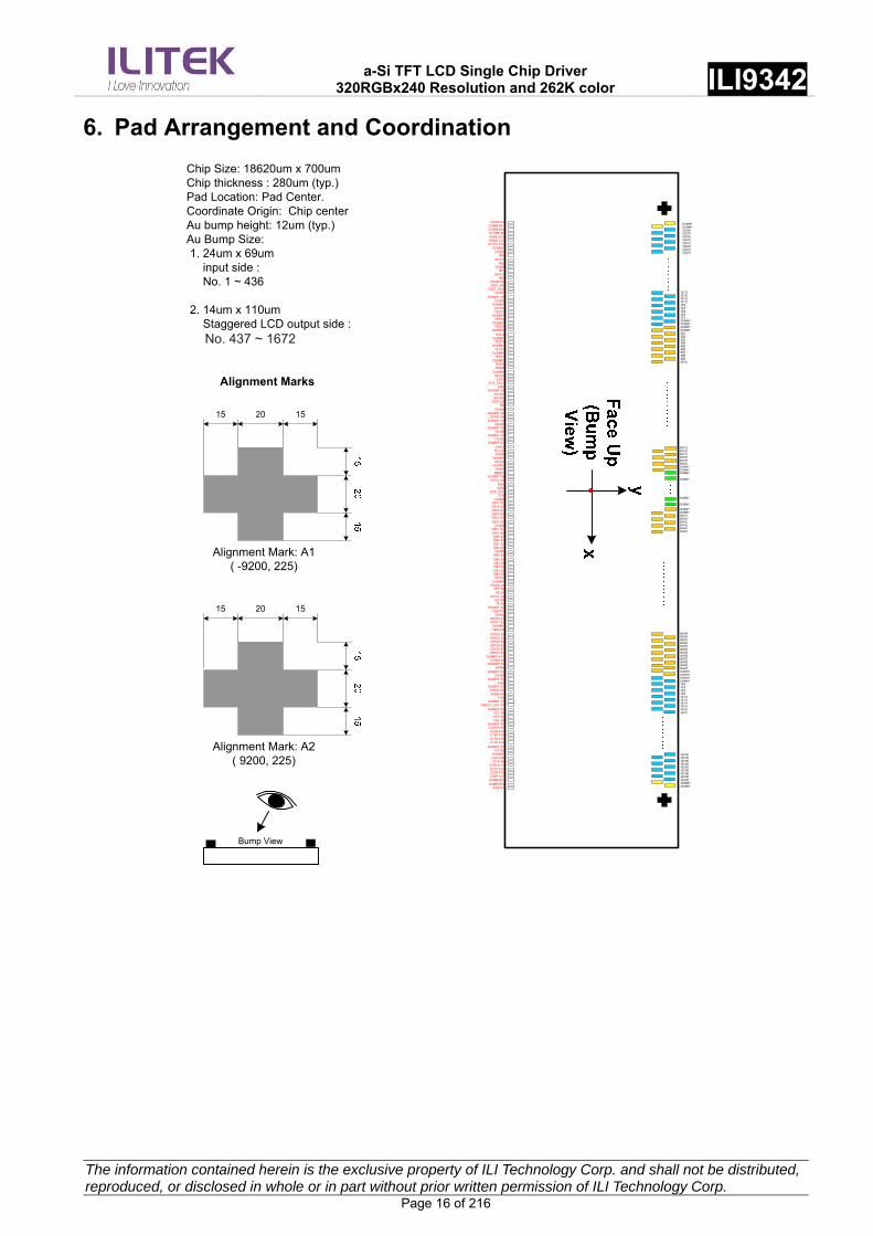
6. Pad Arrangement and Coordination
15 20 15
Alignment Marks
Chip Size: 18620um x 700umChip thickness : 280um (typ.)Pad Location: Pad Center.Coordinate Origin: Chip centerAu bump height: 12um (typ.)Au Bump Size: 1. 24um x 69um
input side : No. 1 ~ 436
2. 14um x 110umStaggered LCD output side :
No. 437 ~ 1672
Bump View
Alignment Mark: A1( -9200, 225)
15 20 15
Alignment Mark: A2( 9200, 225)
G[224]G[226]G[228]G[230]G[232]G[234]G[236]G[238]G[240]DUMMYDUMMY
VCOM X4DUMMYR1DUMMYR2VCORE X8AGND X12DGND X12IOVCC X10
DUMMYDGND
IM3
S[475]S[476]S[477]S[478]S[479]S[480]DUMMYDUMMY
DUMMYDUMMYG[239]G[237]G[235]G[233]G[231]G[229]G[227]G[225]
DUMMYDUMMYS[1]S[2]S[3]S[4]S[5]S[6]S[7]S[8]S[9]S[10]
IOVCCIM2
DGNDIM1
IOVCCIM0
DGND X2TEST_EN
TEST_OSCTEST8
DUMMY X2DGND
DUMMYIOVCCTEST7
DUMMYTEST6
DUMMYTEST5
DUMMYTEST4
DUMMYTEST3
DUMMYTEST2
DUMMYTEST1
DUMMYTEST0DGND
DUMMYIOVCCCSX1
DCX_SCL1SDA
DUMMY X4VSYNCHSYNC
DOTCLKDE
DGNDDUMMY X8
DGND X4DUMMY X3
DGNDDUMMY X3
DGNDDUMMY X3
DGNDDUMMY X3
DGNDTE1 X2DGND
DUMMYIOVCC
DUMMYDGND
RESX1DUMMY X8
IOVCC X4RDXWRX
DCX_SCLCSX
DGNDDB17 X2DB16 X2DB15 X2DB14 X2DB13 X2DB12 X2
DGNDDB11 X2DB10 X2
DB9 X2DB8 X2DB7 X2DB6 X2DGND
DB5 X2DB4 X2DB3 X2DB2 X2DB1 X2DB0 X2IOVCC
DUMMYDGND X4
VPP X3RESX
IOVCC X4VCI X4TE X2
DUMMY X2TESTO1
DGNDGPIO0 X2GPIO1 X2
DUMMYTESTO2
GPIO2 X2GPIO3 X2GPIO4 X2GPIO5 X2GPIO6 X2GPIO7 X2
DUMMY X10DGND X6
DUMMY X2DGND
DUMMY X2DGND
DUMMY X2 VGS
DUMMY X2DGND X5AGND X4
VGSDUMMY 13
VREG1_OUT X2DUMMY X5
VCL X6VGH X6VGL X6
DUMMY X5DDVDH X6C12N X10C12P X10C11N X10C11P X10
DUMMY X3VCI X6
DUMMYC31N X8C31P X8
C21N X 12C21P X12C22N X12C22P X12
DUMMYR3DUMMYR4
VOM X4
G[2]G[4]G[6]G[8]G[10]G[12]G[14]G[16]G[18]G[20]
S[949]S[950]S[951]S[952]S[953]S[954]S[955]S[956]S[957]S[958]S[959]S[960]DUMMYDUMMYDUMMYDUMMY
DUMMYDUMMYS[481]S[482]S[483]S[484]S[485]S[486]
G[17]G[15]G[13]G[11]G[9]G[7]G[5]G[3]G[1]DUMMYDUMMY
DUMMY
DUMMY
DUMMY
DUMMY
a-Si TFT LCD Single Chip Driver
320RGBx240 Resolution and 262K color ILI9342
The information contained herein is the exclusive property of ILI Technology Corp. and shall not be distributed, reproduced, or disclosed in whole or in part without prior written permission of ILI Technology Corp. Page 17 of 216
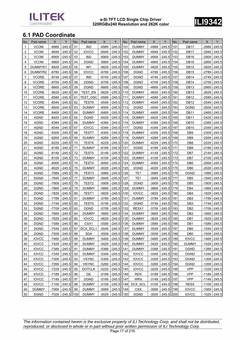
6.1 PAD Coordinate No. Pad name X Y No. Pad name X Y No. Pad name X Y No. Pad name X Y
1 VCOM -8989 -245.5 51 IM3 -6989 -245.5 101 DUMMY -4989 -245.5 151 DB17 -2989 -245.5
2 VCOM -8949 -245.5 52 IOVCC -6949 -245.5 102 DUMMY -4949 -245.5 152 DB17 -2949 -245.5
3 VCOM -8909 -245.5 53 IM2 -6909 -245.5 103 DUMMY -4909 -245.5 153 DB16 -2909 -245.5
4 VCOM -8869 -245.5 54 DGND -6869 -245.5 104 DUMMY -4869 -245.5 154 DB16 -2869 -245.5
5 DUMMYR1 -8829 -245.5 55 IM1 -6829 -245.5 105 DUMMY -4829 -245.5 155 DB15 -2829 -245.5
6 DUMMYR2 -8789 -245.5 56 IOVCC -6789 -245.5 106 DGND -4789 -245.5 156 DB15 -2789 -245.5
7 VCORE -8749 -245.5 57 IM0 -6749 -245.5 107 DGND -4749 -245.5 157 DB14 -2749 -245.5
8 VCORE -8709 -245.5 58 DGND -6709 -245.5 108 DGND -4709 -245.5 158 DB14 -2709 -245.5
9 VCORE -8669 -245.5 59 DGND -6669 -245.5 109 DGND -4669 -245.5 159 DB13 -2669 -245.5
10 VCORE -8629 -245.5 60 TEST_EN -6629 -245.5 110 DUMMY -4629 -245.5 160 DB13 -2629 -245.5
11 VCORE -8589 -245.5 61 TEST_OSC -6589 -245.5 111 DUMMY -4589 -245.5 161 DB12 -2589 -245.5
12 VCORE -8549 -245.5 62 TEST8 -6549 -245.5 112 DUMMY -4549 -245.5 162 DB12 -2549 -245.5
13 VCORE -8509 -245.5 63 DUMMY -6509 -245.5 113 DGND -4509 -245.5 163 DGND -2509 -245.5
14 VCORE -8469 -245.5 64 DUMMY -6469 -245.5 114 DUMMY -4469 -245.5 164 DB11 -2469 -245.5
15 AGND -8429 -245.5 65 DGND -6429 -245.5 115 DUMMY -4429 -245.5 165 DB11 -2429 -245.5
16 AGND -8389 -245.5 66 DUMMY -6389 -245.5 116 DUMMY -4389 -245.5 166 DB10 -2389 -245.5
17 AGND -8349 -245.5 67 IOVCC -6349 -245.5 117 DGND -4349 -245.5 167 DB10 -2349 -245.5
18 AGND -8309 -245.5 68 TEST7 -6309 -245.5 118 DUMMY -4309 -245.5 168 DB9 -2309 -245.5
19 AGND -8269 -245.5 69 DUMMY -6269 -245.5 119 DUMMY -4269 -245.5 169 DB9 -2269 -245.5
20 AGND -8229 -245.5 70 TEST6 -6229 -245.5 120 DUMMY -4229 -245.5 170 DB8 -2229 -245.5
21 AGND -8189 -245.5 71 DUMMY -6189 -245.5 121 DGND -4189 -245.5 171 DB8 -2189 -245.5
22 AGND -8149 -245.5 72 TEST5 -6149 -245.5 122 DUMMY -4149 -245.5 172 DB7 -2149 -245.5
23 AGND -8109 -245.5 73 DUMMY -6109 -245.5 123 DUMMY -4109 -245.5 173 DB7 -2109 -245.5
24 AGND -8069 -245.5 74 TEST4 -6069 -245.5 124 DUMMY -4069 -245.5 174 DB6 -2069 -245.5
25 AGND -8029 -245.5 75 DUMMY -6029 -245.5 125 DGND -4029 -245.5 175 DB6 -2029 -245.5
26 AGND -7989 -245.5 76 TEST3 -5989 -245.5 126 TE1 -3989 -245.5 176 DGND -1989 -245.5
27 DGND -7949 -245.5 77 DUMMY -5949 -245.5 127 TE1 -3949 -245.5 177 DB5 -1949 -245.5
28 DGND -7909 -245.5 78 TEST2 -5909 -245.5 128 DGND -3909 -245.5 178 DB5 -1909 -245.5
29 DGND -7869 -245.5 79 DUMMY -5869 -245.5 129 DUMMY -3869 -245.5 179 DB4 -1869 -245.5
30 DGND -7829 -245.5 80 TEST1 -5829 -245.5 130 IOVCC -3829 -245.5 180 DB4 -1829 -245.5
31 DGND -7789 -245.5 81 DUMMY -5789 -245.5 131 DUMMY -3789 -245.5 181 DB3 -1789 -245.5
32 DGND -7749 -245.5 82 TEST0 -5749 -245.5 132 DGND -3749 -245.5 182 DB3 -1749 -245.5
33 DGND -7709 -245.5 83 DGND -5709 -245.5 133 RESX1 -3709 -245.5 183 DB2 -1709 -245.5
34 DGND -7669 -245.5 84 DUMMY -5669 -245.5 134 DUMMY -3669 -245.5 184 DB2 -1669 -245.5
35 DGND -7629 -245.5 85 IOVCC -5629 -245.5 135 DUMMY -3629 -245.5 185 DB1 -1629 -245.5
36 DGND -7589 -245.5 86 CSX1 -5589 -245.5 136 DUMMY -3589 -245.5 186 DB1 -1589 -245.5
37 DGND -7549 -245.5 87 DCX_SCL1 -5549 -245.5 137 DUMMY -3549 -245.5 187 DB0 -1549 -245.5
38 DGND -7509 -245.5 88 SDA -5509 -245.5 138 DUMMY -3509 -245.5 188 DB0 -1509 -245.5
39 IOVCC -7469 -245.5 89 DUMMY -5469 -245.5 139 DUMMY -3469 -245.5 189 IOVCC -1469 -245.5
40 IOVCC -7429 -245.5 90 DUMMY -5429 -245.5 140 DUMMY -3429 -245.5 190 DUMMY -1429 -245.5
41 IOVCC -7389 -245.5 91 DUMMY -5389 -245.5 141 DUMMY -3389 -245.5 191 DGND -1389 -245.5
42 IOVCC -7349 -245.5 92 DUMMY -5349 -245.5 142 IOVCC -3349 -245.5 192 DGND -1349 -245.5
43 IOVCC -7309 -245.5 93 VSYNC -5309 -245.5 143 IOVCC -3309 -245.5 193 DGND -1309 -245.5
44 IOVCC -7269 -245.5 94 HSYNC -5269 -245.5 144 IOVCC -3269 -245.5 194 DGND -1269 -245.5
45 IOVCC -7229 -245.5 95 DOTCLK -5229 -245.5 145 IOVCC -3229 -245.5 195 VPP -1229 -245.5
46 IOVCC -7189 -245.5 96 DE -5189 -245.5 146 RDX -3189 -245.5 196 VPP -1189 -245.5
47 IOVCC -7149 -245.5 97 DGND -5149 -245.5 147 WRX -3149 -245.5 197 VPP -1149 -245.5
48 IOVCC -7109 -245.5 98 DUMMY -5109 -245.5 148 DCX_SCL -3109 -245.5 198 RESX -1109 -245.5
49 DUMMY -7069 -245.5 99 DUMMY -5069 -245.5 149 CSX -3069 -245.5 199 IOVCC -1069 -245.5
50 DGND -7029 -245.5 100 DUMMY -5029 -245.5 150 DGND -3029 -245.5 200 IOVCC -1029 -245.5

a-Si TFT LCD Single Chip Driver
320RGBx240 Resolution and 262K color ILI9342
The information contained herein is the exclusive property of ILI Technology Corp. and shall not be distributed, reproduced, or disclosed in whole or in part without prior written permission of ILI Technology Corp. Page 18 of 216
No. Pad name X Y No. Pad name X Y No. Pad name X Y No. Pad name X Y
201 IOVCC -989 -245.5 251 DUMMY 1589 -245.5 301 VGL 3589 -245.5 351 C11P 5589 -245.5
202 IOVCC -949 -245.5 252 DGND 1629 -245.5 302 VGL 3629 -245.5 352 C11P 5629 -245.5
203 VCI -909 -245.5 253 DUMMY 1669 -245.5 303 VGL 3669 -245.5 353 C11P 5669 -245.5
204 VCI -869 -245.5 254 DUMMY 1709 -245.5 304 VGL 3709 -245.5 354 C11P 5709 -245.5
205 VCI -829 -245.5 255 VGS 1749 -245.5 305 VGL 3749 -245.5 355 C11P 5749 -245.5
206 VCI -789 -245.5 256 DUMMY 1789 -245.5 306 DUMMY 3789 -245.5 356 C11P 5789 -245.5
207 TE -749 -245.5 257 DUMMY 1829 -245.5 307 DUMMY 3829 -245.5 357 DUMMY 5829 -245.5
208 TE -709 -245.5 258 DGND 1869 -245.5 308 DUMMY 3869 -245.5 358 DUMMY 5869 -245.5
209 DUMMY -669 -245.5 259 DGND 1909 -245.5 309 DUMMY 3909 -245.5 359 DUMMY 5909 -245.5
210 DUMMY -629 -245.5 260 DGND 1949 -245.5 310 DUMMY 3949 -245.5 360 VCI 5949 -245.5
211 TESTO1 -589 -245.5 261 DGND 1989 -245.5 311 DDVDH 3989 -245.5 361 VCI 5989 -245.5
212 DGND -549 -245.5 262 DGND 2029 -245.5 312 DDVDH 4029 -245.5 362 VCI 6029 -245.5
213 GPIO0 -509 -245.5 263 AGND 2069 -245.5 313 DDVDH 4069 -245.5 363 VCI 6069 -245.5
214 GPIO0 -469 -245.5 264 AGND 2109 -245.5 314 DDVDH 4109 -245.5 364 VCI 6109 -245.5
215 GPIO1 -429 -245.5 265 AGND 2149 -245.5 315 DDVDH 4149 -245.5 365 VCI 6149 -245.5
216 GPIO1 -389 -245.5 266 AGND 2189 -245.5 316 DDVDH 4189 -245.5 366 DUMMY 6189 -245.5
217 DUMMY -349 -245.5 267 VGS 2229 -245.5 317 C12N 4229 -245.5 367 C31N 6229 -245.5
218 TESTO2 -309 -245.5 268 DUMMY 2269 -245.5 318 C12N 4269 -245.5 368 C31N 6269 -245.5
219 GPIO2 309 -245.5 269 DUMMY 2309 -245.5 319 C12N 4309 -245.5 369 C31N 6309 -245.5
220 GPIO2 349 -245.5 270 DUMMY 2349 -245.5 320 C12N 4349 -245.5 370 C31N 6349 -245.5
221 GPIO3 389 -245.5 271 DUMMY 2389 -245.5 321 C12N 4389 -245.5 371 C31N 6389 -245.5
222 GPIO3 429 -245.5 272 DUMMY 2429 -245.5 322 C12N 4429 -245.5 372 C31N 6429 -245.5
223 GPIO4 469 -245.5 273 DUMMY 2469 -245.5 323 C12N 4469 -245.5 373 C31N 6469 -245.5
224 GPIO4 509 -245.5 274 DUMMY 2509 -245.5 324 C12N 4509 -245.5 374 C31N 6509 -245.5
225 GPIO5 549 -245.5 275 DUMMY 2549 -245.5 325 C12N 4549 -245.5 375 C31P 6549 -245.5
226 GPIO5 589 -245.5 276 DUMMY 2589 -245.5 326 C12N 4589 -245.5 376 C31P 6589 -245.5
227 GPIO6 629 -245.5 277 DUMMY 2629 -245.5 327 C12P 4629 -245.5 377 C31P 6629 -245.5
228 GPIO6 669 -245.5 278 DUMMY 2669 -245.5 328 C12P 4669 -245.5 378 C31P 6669 -245.5
229 GPIO7 709 -245.5 279 DUMMY 2709 -245.5 329 C12P 4709 -245.5 379 C31P 6709 -245.5
230 GPIO7 749 -245.5 280 DUMMY 2749 -245.5 330 C12P 4749 -245.5 380 C31P 6749 -245.5
231 DUMMY 789 -245.5 281 VREG1_OUT 2789 -245.5 331 C12P 4789 -245.5 381 C31P 6789 -245.5
232 DUMMY 829 -245.5 282 VREG1_OUT 2829 -245.5 332 C12P 4829 -245.5 382 C31P 6829 -245.5
233 DUMMY 869 -245.5 283 DUMMY 2869 -245.5 333 C12P 4869 -245.5 383 C21N 6869 -245.5
234 DUMMY 909 -245.5 284 DUMMY 2909 -245.5 334 C12P 4909 -245.5 384 C21N 6909 -245.5
235 DUMMY 949 -245.5 285 DUMMY 2949 -245.5 335 C12P 4949 -245.5 385 C21N 6949 -245.5
236 DUMMY 989 -245.5 286 DUMMY 2989 -245.5 336 C12P 4989 -245.5 386 C21N 6989 -245.5
237 DUMMY 1029 -245.5 287 DUMMY 3029 -245.5 337 C11N 5029 -245.5 387 C21N 7029 -245.5
238 DUMMY 1069 -245.5 288 VCL 3069 -245.5 338 C11N 5069 -245.5 388 C21N 7069 -245.5
239 DUMMY 1109 -245.5 289 VCL 3109 -245.5 339 C11N 5109 -245.5 389 C21N 7109 -245.5
240 DUMMY 1149 -245.5 290 VCL 3149 -245.5 340 C11N 5149 -245.5 390 C21N 7149 -245.5
241 DGND 1189 -245.5 291 VCL 3189 -245.5 341 C11N 5189 -245.5 391 C21N 7189 -245.5
242 DGND 1229 -245.5 292 VCL 3229 -245.5 342 C11N 5229 -245.5 392 C21N 7229 -245.5
243 DGND 1269 -245.5 293 VCL 3269 -245.5 343 C11N 5269 -245.5 393 C21N 7269 -245.5
244 DGND 1309 -245.5 294 VGH 3309 -245.5 344 C11N 5309 -245.5 394 C21N 7309 -245.5
245 DGND 1349 -245.5 295 VGH 3349 -245.5 345 C11N 5349 -245.5 395 C21P 7349 -245.5
246 DGND 1389 -245.5 296 VGH 3389 -245.5 346 C11N 5389 -245.5 396 C21P 7389 -245.5
247 DUMMY 1429 -245.5 297 VGH 3429 -245.5 347 C11P 5429 -245.5 397 C21P 7429 -245.5
248 DUMMY 1469 -245.5 298 VGH 3469 -245.5 348 C11P 5469 -245.5 398 C21P 7469 -245.5
249 DGND 1509 -245.5 299 VGH 3509 -245.5 349 C11P 5509 -245.5 399 C21P 7509 -245.5
250 DUMMY 1549 -245.5 300 VGL 3549 -245.5 350 C11P 5549 -245.5 400 C21P 7549 -245.5
a-Si TFT LCD Single Chip Driver
320RGBx240 Resolution and 262K color ILI9342
The information contained herein is the exclusive property of ILI Technology Corp. and shall not be distributed, reproduced, or disclosed in whole or in part without prior written permission of ILI Technology Corp. Page 19 of 216
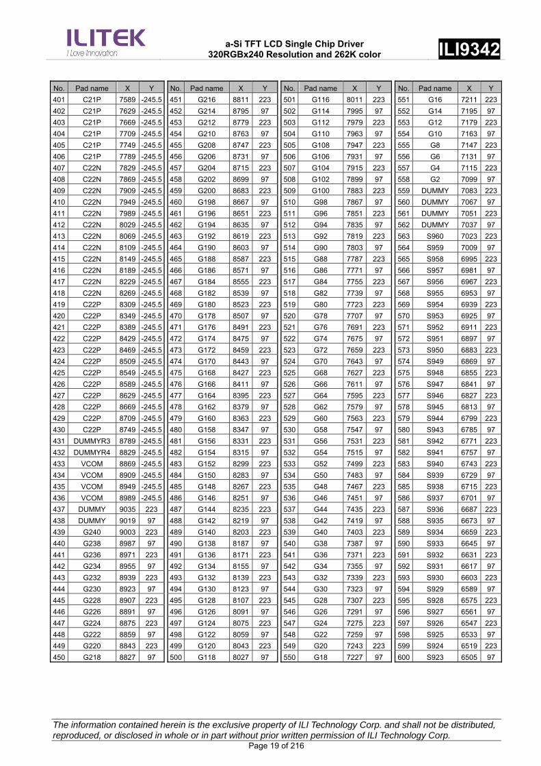
No. Pad name X Y No. Pad name X Y No. Pad name X Y No. Pad name X Y
401 C21P 7589 -245.5 451 G216 8811 223 501 G116 8011 223 551 G16 7211 223
402 C21P 7629 -245.5 452 G214 8795 97 502 G114 7995 97 552 G14 7195 97
403 C21P 7669 -245.5 453 G212 8779 223 503 G112 7979 223 553 G12 7179 223
404 C21P 7709 -245.5 454 G210 8763 97 504 G110 7963 97 554 G10 7163 97
405 C21P 7749 -245.5 455 G208 8747 223 505 G108 7947 223 555 G8 7147 223
406 C21P 7789 -245.5 456 G206 8731 97 506 G106 7931 97 556 G6 7131 97
407 C22N 7829 -245.5 457 G204 8715 223 507 G104 7915 223 557 G4 7115 223
408 C22N 7869 -245.5 458 G202 8699 97 508 G102 7899 97 558 G2 7099 97
409 C22N 7909 -245.5 459 G200 8683 223 509 G100 7883 223 559 DUMMY 7083 223
410 C22N 7949 -245.5 460 G198 8667 97 510 G98 7867 97 560 DUMMY 7067 97
411 C22N 7989 -245.5 461 G196 8651 223 511 G96 7851 223 561 DUMMY 7051 223
412 C22N 8029 -245.5 462 G194 8635 97 512 G94 7835 97 562 DUMMY 7037 97
413 C22N 8069 -245.5 463 G192 8619 223 513 G92 7819 223 563 S960 7023 223
414 C22N 8109 -245.5 464 G190 8603 97 514 G90 7803 97 564 S959 7009 97
415 C22N 8149 -245.5 465 G188 8587 223 515 G88 7787 223 565 S958 6995 223
416 C22N 8189 -245.5 466 G186 8571 97 516 G86 7771 97 566 S957 6981 97
417 C22N 8229 -245.5 467 G184 8555 223 517 G84 7755 223 567 S956 6967 223
418 C22N 8269 -245.5 468 G182 8539 97 518 G82 7739 97 568 S955 6953 97
419 C22P 8309 -245.5 469 G180 8523 223 519 G80 7723 223 569 S954 6939 223
420 C22P 8349 -245.5 470 G178 8507 97 520 G78 7707 97 570 S953 6925 97
421 C22P 8389 -245.5 471 G176 8491 223 521 G76 7691 223 571 S952 6911 223
422 C22P 8429 -245.5 472 G174 8475 97 522 G74 7675 97 572 S951 6897 97
423 C22P 8469 -245.5 473 G172 8459 223 523 G72 7659 223 573 S950 6883 223
424 C22P 8509 -245.5 474 G170 8443 97 524 G70 7643 97 574 S949 6869 97
425 C22P 8549 -245.5 475 G168 8427 223 525 G68 7627 223 575 S948 6855 223
426 C22P 8589 -245.5 476 G166 8411 97 526 G66 7611 97 576 S947 6841 97
427 C22P 8629 -245.5 477 G164 8395 223 527 G64 7595 223 577 S946 6827 223
428 C22P 8669 -245.5 478 G162 8379 97 528 G62 7579 97 578 S945 6813 97
429 C22P 8709 -245.5 479 G160 8363 223 529 G60 7563 223 579 S944 6799 223
430 C22P 8749 -245.5 480 G158 8347 97 530 G58 7547 97 580 S943 6785 97
431 DUMMYR3 8789 -245.5 481 G156 8331 223 531 G56 7531 223 581 S942 6771 223
432 DUMMYR4 8829 -245.5 482 G154 8315 97 532 G54 7515 97 582 S941 6757 97
433 VCOM 8869 -245.5 483 G152 8299 223 533 G52 7499 223 583 S940 6743 223
434 VCOM 8909 -245.5 484 G150 8283 97 534 G50 7483 97 584 S939 6729 97
435 VCOM 8949 -245.5 485 G148 8267 223 535 G48 7467 223 585 S938 6715 223
436 VCOM 8989 -245.5 486 G146 8251 97 536 G46 7451 97 586 S937 6701 97
437 DUMMY 9035 223 487 G144 8235 223 537 G44 7435 223 587 S936 6687 223
438 DUMMY 9019 97 488 G142 8219 97 538 G42 7419 97 588 S935 6673 97
439 G240 9003 223 489 G140 8203 223 539 G40 7403 223 589 S934 6659 223
440 G238 8987 97 490 G138 8187 97 540 G38 7387 97 590 S933 6645 97
441 G236 8971 223 491 G136 8171 223 541 G36 7371 223 591 S932 6631 223
442 G234 8955 97 492 G134 8155 97 542 G34 7355 97 592 S931 6617 97
443 G232 8939 223 493 G132 8139 223 543 G32 7339 223 593 S930 6603 223
444 G230 8923 97 494 G130 8123 97 544 G30 7323 97 594 S929 6589 97
445 G228 8907 223 495 G128 8107 223 545 G28 7307 223 595 S928 6575 223
446 G226 8891 97 496 G126 8091 97 546 G26 7291 97 596 S927 6561 97
447 G224 8875 223 497 G124 8075 223 547 G24 7275 223 597 S926 6547 223
448 G222 8859 97 498 G122 8059 97 548 G22 7259 97 598 S925 6533 97
449 G220 8843 223 499 G120 8043 223 549 G20 7243 223 599 S924 6519 223
450 G218 8827 97 500 G118 8027 97 550 G18 7227 97 600 S923 6505 97

a-Si TFT LCD Single Chip Driver
320RGBx240 Resolution and 262K color ILI9342
The information contained herein is the exclusive property of ILI Technology Corp. and shall not be distributed, reproduced, or disclosed in whole or in part without prior written permission of ILI Technology Corp. Page 20 of 216
No. Pad name X Y No. Pad name X Y No. Pad name X Y No. Pad name X Y
601 S922 6491 223 651 S872 5791 223 701 S822 5091 223 751 S772 4391 223
602 S921 6477 97 652 S871 5777 97 702 S821 5077 97 752 S771 4377 97
603 S920 6463 223 653 S870 5763 223 703 S820 5063 223 753 S770 4363 223
604 S919 6449 97 654 S869 5749 97 704 S819 5049 97 754 S769 4349 97
605 S918 6435 223 655 S868 5735 223 705 S818 5035 223 755 S768 4335 223
606 S917 6421 97 656 S867 5721 97 706 S817 5021 97 756 S767 4321 97
607 S916 6407 223 657 S866 5707 223 707 S816 5007 223 757 S766 4307 223
608 S915 6393 97 658 S865 5693 97 708 S815 4993 97 758 S765 4293 97
609 S914 6379 223 659 S864 5679 223 709 S814 4979 223 759 S764 4279 223
610 S913 6365 97 660 S863 5665 97 710 S813 4965 97 760 S763 4265 97
611 S912 6351 223 661 S862 5651 223 711 S812 4951 223 761 S762 4251 223
612 S911 6337 97 662 S861 5637 97 712 S811 4937 97 762 S761 4237 97
613 S910 6323 223 663 S860 5623 223 713 S810 4923 223 763 S760 4223 223
614 S909 6309 97 664 S859 5609 97 714 S809 4909 97 764 S759 4209 97
615 S908 6295 223 665 S858 5595 223 715 S808 4895 223 765 S758 4195 223
616 S907 6281 97 666 S857 5581 97 716 S807 4881 97 766 S757 4181 97
617 S906 6267 223 667 S856 5567 223 717 S806 4867 223 767 S756 4167 223
618 S905 6253 97 668 S855 5553 97 718 S805 4853 97 768 S755 4153 97
619 S904 6239 223 669 S854 5539 223 719 S804 4839 223 769 S754 4139 223
620 S903 6225 97 670 S853 5525 97 720 S803 4825 97 770 S753 4125 97
621 S902 6211 223 671 S852 5511 223 721 S802 4811 223 771 S752 4111 223
622 S901 6197 97 672 S851 5497 97 722 S801 4797 97 772 S751 4097 97
623 S900 6183 223 673 S850 5483 223 723 S800 4783 223 773 S750 4083 223
624 S899 6169 97 674 S849 5469 97 724 S799 4769 97 774 S749 4069 97
625 S898 6155 223 675 S848 5455 223 725 S798 4755 223 775 S748 4055 223
626 S897 6141 97 676 S847 5441 97 726 S797 4741 97 776 S747 4041 97
627 S896 6127 223 677 S846 5427 223 727 S796 4727 223 777 S746 4027 223
628 S895 6113 97 678 S845 5413 97 728 S795 4713 97 778 S745 4013 97
629 S894 6099 223 679 S844 5399 223 729 S794 4699 223 779 S744 3999 223
630 S893 6085 97 680 S843 5385 97 730 S793 4685 97 780 S743 3985 97
631 S892 6071 223 681 S842 5371 223 731 S792 4671 223 781 S742 3971 223
632 S891 6057 97 682 S841 5357 97 732 S791 4657 97 782 S741 3957 97
633 S890 6043 223 683 S840 5343 223 733 S790 4643 223 783 S740 3943 223
634 S889 6029 97 684 S839 5329 97 734 S789 4629 97 784 S739 3929 97
635 S888 6015 223 685 S838 5315 223 735 S788 4615 223 785 S738 3915 223
636 S887 6001 97 686 S837 5301 97 736 S787 4601 97 786 S737 3901 97
637 S886 5987 223 687 S836 5287 223 737 S786 4587 223 787 S736 3887 223
638 S885 5973 97 688 S835 5273 97 738 S785 4573 97 788 S735 3873 97
639 S884 5959 223 689 S834 5259 223 739 S784 4559 223 789 S734 3859 223
640 S883 5945 97 690 S833 5245 97 740 S783 4545 97 790 S733 3845 97
641 S882 5931 223 691 S832 5231 223 741 S782 4531 223 791 S732 3831 223
642 S881 5917 97 692 S831 5217 97 742 S781 4517 97 792 S731 3817 97
643 S880 5903 223 693 S830 5203 223 743 S780 4503 223 793 S730 3803 223
644 S879 5889 97 694 S829 5189 97 744 S779 4489 97 794 S729 3789 97
645 S878 5875 223 695 S828 5175 223 745 S778 4475 223 795 S728 3775 223
646 S877 5861 97 696 S827 5161 97 746 S777 4461 97 796 S727 3761 97
647 S876 5847 223 697 S826 5147 223 747 S776 4447 223 797 S726 3747 223
648 S875 5833 97 698 S825 5133 97 748 S775 4433 97 798 S725 3733 97
649 S874 5819 223 699 S824 5119 223 749 S774 4419 223 799 S724 3719 223
650 S873 5805 97 700 S823 5105 97 750 S773 4405 97 800 S723 3705 97

a-Si TFT LCD Single Chip Driver
320RGBx240 Resolution and 262K color ILI9342
The information contained herein is the exclusive property of ILI Technology Corp. and shall not be distributed, reproduced, or disclosed in whole or in part without prior written permission of ILI Technology Corp. Page 21 of 216
No. Pad name X Y No. Pad name X Y No. Pad name X Y No. Pad name X Y
801 S722 3691 223 851 S672 2991 223 901 S622 2291 223 951 S572 1591 223
802 S721 3677 97 852 S671 2977 97 902 S621 2277 97 952 S571 1577 97
803 S720 3663 223 853 S670 2963 223 903 S620 2263 223 953 S570 1563 223
804 S719 3649 97 854 S669 2949 97 904 S619 2249 97 954 S569 1549 97
805 S718 3635 223 855 S668 2935 223 905 S618 2235 223 955 S568 1535 223
806 S717 3621 97 856 S667 2921 97 906 S617 2221 97 956 S567 1521 97
807 S716 3607 223 857 S666 2907 223 907 S616 2207 223 957 S566 1507 223
808 S715 3593 97 858 S665 2893 97 908 S615 2193 97 958 S565 1493 97
809 S714 3579 223 859 S664 2879 223 909 S614 2179 223 959 S564 1479 223
810 S713 3565 97 860 S663 2865 97 910 S613 2165 97 960 S563 1465 97
811 S712 3551 223 861 S662 2851 223 911 S612 2151 223 961 S562 1451 223
812 S711 3537 97 862 S661 2837 97 912 S611 2137 97 962 S561 1437 97
813 S710 3523 223 863 S660 2823 223 913 S610 2123 223 963 S560 1423 223
814 S709 3509 97 864 S659 2809 97 914 S609 2109 97 964 S559 1409 97
815 S708 3495 223 865 S658 2795 223 915 S608 2095 223 965 S558 1395 223
816 S707 3481 97 866 S657 2781 97 916 S607 2081 97 966 S557 1381 97
817 S706 3467 223 867 S656 2767 223 917 S606 2067 223 967 S556 1367 223
818 S705 3453 97 868 S655 2753 97 918 S605 2053 97 968 S555 1353 97
819 S704 3439 223 869 S654 2739 223 919 S604 2039 223 969 S554 1339 223
820 S703 3425 97 870 S653 2725 97 920 S603 2025 97 970 S553 1325 97
821 S702 3411 223 871 S652 2711 223 921 S602 2011 223 971 S552 1311 223
822 S701 3397 97 872 S651 2697 97 922 S601 1997 97 972 S551 1297 97
823 S700 3383 223 873 S650 2683 223 923 S600 1983 223 973 S550 1283 223
824 S699 3369 97 874 S649 2669 97 924 S599 1969 97 974 S549 1269 97
825 S698 3355 223 875 S648 2655 223 925 S598 1955 223 975 S548 1255 223
826 S697 3341 97 876 S647 2641 97 926 S597 1941 97 976 S547 1241 97
827 S696 3327 223 877 S646 2627 223 927 S596 1927 223 977 S546 1227 223
828 S695 3313 97 878 S645 2613 97 928 S595 1913 97 978 S545 1213 97
829 S694 3299 223 879 S644 2599 223 929 S594 1899 223 979 S544 1199 223
830 S693 3285 97 880 S643 2585 97 930 S593 1885 97 980 S543 1185 97
831 S692 3271 223 881 S642 2571 223 931 S592 1871 223 981 S542 1171 223
832 S691 3257 97 882 S641 2557 97 932 S591 1857 97 982 S541 1157 97
833 S690 3243 223 883 S640 2543 223 933 S590 1843 223 983 S540 1143 223
834 S689 3229 97 884 S639 2529 97 934 S589 1829 97 984 S539 1129 97
835 S688 3215 223 885 S638 2515 223 935 S588 1815 223 985 S538 1115 223
836 S687 3201 97 886 S637 2501 97 936 S587 1801 97 986 S537 1101 97
837 S686 3187 223 887 S636 2487 223 937 S586 1787 223 987 S536 1087 223
838 S685 3173 97 888 S635 2473 97 938 S585 1773 97 988 S535 1073 97
839 S684 3159 223 889 S634 2459 223 939 S584 1759 223 989 S534 1059 223
840 S683 3145 97 890 S633 2445 97 940 S583 1745 97 990 S533 1045 97
841 S682 3131 223 891 S632 2431 223 941 S582 1731 223 991 S532 1031 223
842 S681 3117 97 892 S631 2417 97 942 S581 1717 97 992 S531 1017 97
843 S680 3103 223 893 S630 2403 223 943 S580 1703 223 993 S530 1003 223
844 S679 3089 97 894 S629 2389 97 944 S579 1689 97 994 S529 989 97
845 S678 3075 223 895 S628 2375 223 945 S578 1675 223 995 S528 975 223
846 S677 3061 97 896 S627 2361 97 946 S577 1661 97 996 S527 961 97
847 S676 3047 223 897 S626 2347 223 947 S576 1647 223 997 S526 947 223
848 S675 3033 97 898 S625 2333 97 948 S575 1633 97 998 S525 933 97
849 S674 3019 223 899 S624 2319 223 949 S574 1619 223 999 S524 919 223
850 S673 3005 97 900 S623 2305 97 950 S573 1605 97 1000 S523 905 97

a-Si TFT LCD Single Chip Driver
320RGBx240 Resolution and 262K color ILI9342
The information contained herein is the exclusive property of ILI Technology Corp. and shall not be distributed, reproduced, or disclosed in whole or in part without prior written permission of ILI Technology Corp. Page 22 of 216
No. Pad name X Y No. Pad name X Y No. Pad name X Y No. Pad name X Y
1001 S522 891 223 1051 DUMMY 107 223 1101 S446 -793 97 1151 S396 -1493 97
1002 S521 877 97 1052 DUMMY 79 223 1102 S445 -807 223 1152 S395 -1507 223
1003 S520 863 223 1053 DUMMY 51 223 1103 S444 -821 97 1153 S394 -1521 97
1004 S519 849 97 1054 DUMMY 23 223 1104 S443 -835 223 1154 S393 -1535 223
1005 S518 835 223 1055 DUMMY -23 223 1105 S442 -849 97 1155 S392 -1549 97
1006 S517 821 97 1056 DUMMY -51 223 1106 S441 -863 223 1156 S391 -1563 223
1007 S516 807 223 1057 DUMMY -79 223 1107 S440 -877 97 1157 S390 -1577 97
1008 S515 793 97 1058 DUMMY -107 223 1108 S439 -891 223 1158 S389 -1591 223
1009 S514 779 223 1059 DUMMY -135 223 1109 S438 -905 97 1159 S388 -1605 97
1010 S513 765 97 1060 DUMMY -163 223 1110 S437 -919 223 1160 S387 -1619 223
1011 S512 751 223 1061 DUMMY -191 223 1111 S436 -933 97 1161 S386 -1633 97
1012 S511 737 97 1062 DUMMY -219 223 1112 S435 -947 223 1162 S385 -1647 223
1013 S510 723 223 1063 DUMMY -247 223 1113 S434 -961 97 1163 S384 -1661 97
1014 S509 709 97 1064 DUMMY -275 223 1114 S433 -975 223 1164 S383 -1675 223
1015 S508 695 223 1065 DUMMY -289 97 1115 S432 -989 97 1165 S382 -1689 97
1016 S507 681 97 1066 DUMMY -303 223 1116 S431 -1003 223 1166 S381 -1703 223
1017 S506 667 223 1067 S480 -317 97 1117 S430 -1017 97 1167 S380 -1717 97
1018 S505 653 97 1068 S479 -331 223 1118 S429 -1031 223 1168 S379 -1731 223
1019 S504 639 223 1069 S478 -345 97 1119 S428 -1045 97 1169 S378 -1745 97
1020 S503 625 97 1070 S477 -359 223 1120 S427 -1059 223 1170 S377 -1759 223
1021 S502 611 223 1071 S476 -373 97 1121 S426 -1073 97 1171 S376 -1773 97
1022 S501 597 97 1072 S475 -387 223 1122 S425 -1087 223 1172 S375 -1787 223
1023 S500 583 223 1073 S474 -401 97 1123 S424 -1101 97 1173 S374 -1801 97
1024 S499 569 97 1074 S473 -415 223 1124 S423 -1115 223 1174 S373 -1815 223
1025 S498 555 223 1075 S472 -429 97 1125 S422 -1129 97 1175 S372 -1829 97
1026 S497 541 97 1076 S471 -443 223 1126 S421 -1143 223 1176 S371 -1843 223
1027 S496 527 223 1077 S470 -457 97 1127 S420 -1157 97 1177 S370 -1857 97
1028 S495 513 97 1078 S469 -471 223 1128 S419 -1171 223 1178 S369 -1871 223
1029 S494 499 223 1079 S468 -485 97 1129 S418 -1185 97 1179 S368 -1885 97
1030 S493 485 97 1080 S467 -499 223 1130 S417 -1199 223 1180 S367 -1899 223
1031 S492 471 223 1081 S466 -513 97 1131 S416 -1213 97 1181 S366 -1913 97
1032 S491 457 97 1082 S465 -527 223 1132 S415 -1227 223 1182 S365 -1927 223
1033 S490 443 223 1083 S464 -541 97 1133 S414 -1241 97 1183 S364 -1941 97
1034 S489 429 97 1084 S463 -555 223 1134 S413 -1255 223 1184 S363 -1955 223
1035 S488 415 223 1085 S462 -569 97 1135 S412 -1269 97 1185 S362 -1969 97
1036 S487 401 97 1086 S461 -583 223 1136 S411 -1283 223 1186 S361 -1983 223
1037 S486 387 223 1087 S460 -597 97 1137 S410 -1297 97 1187 S360 -1997 97
1038 S485 373 97 1088 S459 -611 223 1138 S409 -1311 223 1188 S359 -2011 223
1039 S484 359 223 1089 S458 -625 97 1139 S408 -1325 97 1189 S358 -2025 97
1040 S483 345 97 1090 S457 -639 223 1140 S407 -1339 223 1190 S357 -2039 223
1041 S482 331 223 1091 S456 -653 97 1141 S406 -1353 97 1191 S356 -2053 97
1042 S481 317 97 1092 S455 -667 223 1142 S405 -1367 223 1192 S355 -2067 223
1043 DUMMY 303 223 1093 S454 -681 97 1143 S404 -1381 97 1193 S354 -2081 97
1044 DUMMY 289 97 1094 S453 -695 223 1144 S403 -1395 223 1194 S353 -2095 223
1045 DUMMY 275 223 1095 S452 -709 97 1145 S402 -1409 97 1195 S352 -2109 97
1046 DUMMY 247 223 1096 S451 -723 223 1146 S401 -1423 223 1196 S351 -2123 223
1047 DUMMY 219 223 1097 S450 -737 97 1147 S400 -1437 97 1197 S350 -2137 97
1048 DUMMY 191 223 1098 S449 -751 223 1148 S399 -1451 223 1198 S349 -2151 223
1049 DUMMY 163 223 1099 S448 -765 97 1149 S398 -1465 97 1199 S348 -2165 97
1050 DUMMY 135 223 1100 S447 -779 223 1150 S397 -1479 223 1200 S347 -2179 223

a-Si TFT LCD Single Chip Driver
320RGBx240 Resolution and 262K color ILI9342
The information contained herein is the exclusive property of ILI Technology Corp. and shall not be distributed, reproduced, or disclosed in whole or in part without prior written permission of ILI Technology Corp. Page 23 of 216
No. Pad name X Y No. Pad name X Y No. Pad name X Y No. Pad name X Y
1201 S346 -2193 97 1251 S296 -2893 97 1301 S246 -3593 97 1351 S196 -4293 97
1202 S345 -2207 223 1252 S295 -2907 223 1302 S245 -3607 223 1352 S195 -4307 223
1203 S344 -2221 97 1253 S294 -2921 97 1303 S244 -3621 97 1353 S194 -4321 97
1204 S343 -2235 223 1254 S293 -2935 223 1304 S243 -3635 223 1354 S193 -4335 223
1205 S342 -2249 97 1255 S292 -2949 97 1305 S242 -3649 97 1355 S192 -4349 97
1206 S341 -2263 223 1256 S291 -2963 223 1306 S241 -3663 223 1356 S191 -4363 223
1207 S340 -2277 97 1257 S290 -2977 97 1307 S240 -3677 97 1357 S190 -4377 97
1208 S339 -2291 223 1258 S289 -2991 223 1308 S239 -3691 223 1358 S189 -4391 223
1209 S338 -2305 97 1259 S288 -3005 97 1309 S238 -3705 97 1359 S188 -4405 97
1210 S337 -2319 223 1260 S287 -3019 223 1310 S237 -3719 223 1360 S187 -4419 223
1211 S336 -2333 97 1261 S286 -3033 97 1311 S236 -3733 97 1361 S186 -4433 97
1212 S335 -2347 223 1262 S285 -3047 223 1312 S235 -3747 223 1362 S185 -4447 223
1213 S334 -2361 97 1263 S284 -3061 97 1313 S234 -3761 97 1363 S184 -4461 97
1214 S333 -2375 223 1264 S283 -3075 223 1314 S233 -3775 223 1364 S183 -4475 223
1215 S332 -2389 97 1265 S282 -3089 97 1315 S232 -3789 97 1365 S182 -4489 97
1216 S331 -2403 223 1266 S281 -3103 223 1316 S231 -3803 223 1366 S181 -4503 223
1217 S330 -2417 97 1267 S280 -3117 97 1317 S230 -3817 97 1367 S180 -4517 97
1218 S329 -2431 223 1268 S279 -3131 223 1318 S229 -3831 223 1368 S179 -4531 223
1219 S328 -2445 97 1269 S278 -3145 97 1319 S228 -3845 97 1369 S178 -4545 97
1220 S327 -2459 223 1270 S277 -3159 223 1320 S227 -3859 223 1370 S177 -4559 223
1221 S326 -2473 97 1271 S276 -3173 97 1321 S226 -3873 97 1371 S176 -4573 97
1222 S325 -2487 223 1272 S275 -3187 223 1322 S225 -3887 223 1372 S175 -4587 223
1223 S324 -2501 97 1273 S274 -3201 97 1323 S224 -3901 97 1373 S174 -4601 97
1224 S323 -2515 223 1274 S273 -3215 223 1324 S223 -3915 223 1374 S173 -4615 223
1225 S322 -2529 97 1275 S272 -3229 97 1325 S222 -3929 97 1375 S172 -4629 97
1226 S321 -2543 223 1276 S271 -3243 223 1326 S221 -3943 223 1376 S171 -4643 223
1227 S320 -2557 97 1277 S270 -3257 97 1327 S220 -3957 97 1377 S170 -4657 97
1228 S319 -2571 223 1278 S269 -3271 223 1328 S219 -3971 223 1378 S169 -4671 223
1229 S318 -2585 97 1279 S268 -3285 97 1329 S218 -3985 97 1379 S168 -4685 97
1230 S317 -2599 223 1280 S267 -3299 223 1330 S217 -3999 223 1380 S167 -4699 223
1231 S316 -2613 97 1281 S266 -3313 97 1331 S216 -4013 97 1381 S166 -4713 97
1232 S315 -2627 223 1282 S265 -3327 223 1332 S215 -4027 223 1382 S165 -4727 223
1233 S314 -2641 97 1283 S264 -3341 97 1333 S214 -4041 97 1383 S164 -4741 97
1234 S313 -2655 223 1284 S263 -3355 223 1334 S213 -4055 223 1384 S163 -4755 223
1235 S312 -2669 97 1285 S262 -3369 97 1335 S212 -4069 97 1385 S162 -4769 97
1236 S311 -2683 223 1286 S261 -3383 223 1336 S211 -4083 223 1386 S161 -4783 223
1237 S310 -2697 97 1287 S260 -3397 97 1337 S210 -4097 97 1387 S160 -4797 97
1238 S309 -2711 223 1288 S259 -3411 223 1338 S209 -4111 223 1388 S159 -4811 223
1239 S308 -2725 97 1289 S258 -3425 97 1339 S208 -4125 97 1389 S158 -4825 97
1240 S307 -2739 223 1290 S257 -3439 223 1340 S207 -4139 223 1390 S157 -4839 223
1241 S306 -2753 97 1291 S256 -3453 97 1341 S206 -4153 97 1391 S156 -4853 97
1242 S305 -2767 223 1292 S255 -3467 223 1342 S205 -4167 223 1392 S155 -4867 223
1243 S304 -2781 97 1293 S254 -3481 97 1343 S204 -4181 97 1393 S154 -4881 97
1244 S303 -2795 223 1294 S253 -3495 223 1344 S203 -4195 223 1394 S153 -4895 223
1245 S302 -2809 97 1295 S252 -3509 97 1345 S202 -4209 97 1395 S152 -4909 97
1246 S301 -2823 223 1296 S251 -3523 223 1346 S201 -4223 223 1396 S151 -4923 223
1247 S300 -2837 97 1297 S250 -3537 97 1347 S200 -4237 97 1397 S150 -4937 97
1248 S299 -2851 223 1298 S249 -3551 223 1348 S199 -4251 223 1398 S149 -4951 223
1249 S298 -2865 97 1299 S248 -3565 97 1349 S198 -4265 97 1399 S148 -4965 97
1250 S297 -2879 223 1300 S247 -3579 223 1350 S197 -4279 223 1400 S147 -4979 223

a-Si TFT LCD Single Chip Driver
320RGBx240 Resolution and 262K color ILI9342
The information contained herein is the exclusive property of ILI Technology Corp. and shall not be distributed, reproduced, or disclosed in whole or in part without prior written permission of ILI Technology Corp. Page 24 of 216
No. Pad name X Y No. Pad name X Y No. Pad name X Y No. Pad name X Y
1401 S146 -4993 97 1451 S96 -5693 97 1501 S46 -6393 97 1551 G1 -7099 97
1402 S145 -5007 223 1452 S95 -5707 223 1502 S45 -6407 223 1552 G3 -7115 223
1403 S144 -5021 97 1453 S94 -5721 97 1503 S44 -6421 97 1553 G5 -7131 97
1404 S143 -5035 223 1454 S93 -5735 223 1504 S43 -6435 223 1554 G7 -7147 223
1405 S142 -5049 97 1455 S92 -5749 97 1505 S42 -6449 97 1555 G9 -7163 97
1406 S141 -5063 223 1456 S91 -5763 223 1506 S41 -6463 223 1556 G11 -7179 223
1407 S140 -5077 97 1457 S90 -5777 97 1507 S40 -6477 97 1557 G13 -7195 97
1408 S139 -5091 223 1458 S89 -5791 223 1508 S39 -6491 223 1558 G15 -7211 223
1409 S138 -5105 97 1459 S88 -5805 97 1509 S38 -6505 97 1559 G17 -7227 97
1410 S137 -5119 223 1460 S87 -5819 223 1510 S37 -6519 223 1560 G19 -7243 223
1411 S136 -5133 97 1461 S86 -5833 97 1511 S36 -6533 97 1561 G21 -7259 97
1412 S135 -5147 223 1462 S85 -5847 223 1512 S35 -6547 223 1562 G23 -7275 223
1413 S134 -5161 97 1463 S84 -5861 97 1513 S34 -6561 97 1563 G25 -7291 97
1414 S133 -5175 223 1464 S83 -5875 223 1514 S33 -6575 223 1564 G27 -7307 223
1415 S132 -5189 97 1465 S82 -5889 97 1515 S32 -6589 97 1565 G29 -7323 97
1416 S131 -5203 223 1466 S81 -5903 223 1516 S31 -6603 223 1566 G31 -7339 223
1417 S130 -5217 97 1467 S80 -5917 97 1517 S30 -6617 97 1567 G33 -7355 97
1418 S129 -5231 223 1468 S79 -5931 223 1518 S29 -6631 223 1568 G35 -7371 223
1419 S128 -5245 97 1469 S78 -5945 97 1519 S28 -6645 97 1669 G37 -7387 97
1420 S127 -5259 223 1470 S77 -5959 223 1520 S27 -6659 223 1570 G39 -7403 223
1421 S126 -5273 97 1471 S76 -5973 97 1521 S26 -6673 97 1571 G41 -7419 97
1422 S125 -5287 223 1472 S75 -5987 223 1522 S25 -6687 223 1572 G43 -7435 223
1423 S124 -5301 97 1473 S74 -6001 97 1523 S24 -6701 97 1573 G45 -7451 97
1424 S123 -5315 223 1474 S73 -6015 223 1524 S23 -6715 223 1574 G47 -7467 223
1425 S122 -5329 97 1475 S72 -6029 97 1525 S22 -6729 97 1575 G49 -7483 97
1426 S121 -5343 223 1476 S71 -6043 223 1526 S21 -6743 223 1576 G51 -7499 223
1427 S120 -5357 97 1477 S70 -6057 97 1527 S20 -6757 97 1577 G53 -7515 97
1428 S119 -5371 223 1478 S69 -6071 223 1528 S19 -6771 223 1578 G55 -7531 223
1429 S118 -5385 97 1479 S68 -6085 97 1529 S18 -6785 97 1579 G57 -7547 97
1430 S117 -5399 223 1480 S67 -6099 223 1530 S17 -6799 223 1580 G59 -7563 223
1431 S116 -5413 97 1481 S66 -6113 97 1531 S16 -6813 97 1581 G61 -7579 97
1432 S115 -5427 223 1482 S65 -6127 223 1532 S15 -6827 223 1582 G63 -7595 223
1433 S114 -5441 97 1483 S64 -6141 97 1533 S14 -6841 97 1583 G65 -7611 97
1434 S113 -5455 223 1484 S63 -6155 223 1534 S13 -6855 223 1584 G67 -7627 223
1435 S112 -5469 97 1485 S62 -6169 97 1535 S12 -6869 97 1585 G69 -7643 97
1436 S111 -5483 223 1486 S61 -6183 223 1536 S11 -6883 223 1586 G71 -7659 223
1437 S110 -5497 97 1487 S60 -6197 97 1537 S10 -6897 97 1587 G73 -7675 97
1438 S109 -5511 223 1488 S59 -6211 223 1538 S9 -6911 223 1588 G75 -7691 223
1439 S108 -5525 97 1489 S58 -6225 97 1539 S8 -6925 97 1589 G77 -7707 97
1440 S107 -5539 223 1490 S57 -6239 223 1540 S7 -6939 223 1590 G79 -7723 223
1441 S106 -5553 97 1491 S56 -6253 97 1541 S6 -6953 97 1591 G81 -7739 97
1442 S105 -5567 223 1492 S55 -6267 223 1542 S5 -6967 223 1592 G83 -7755 223
1443 S104 -5581 97 1493 S54 -6281 97 1543 S4 -6981 97 1593 G85 -7771 97
1444 S103 -5595 223 1494 S53 -6295 223 1544 S3 -6995 223 1594 G87 -7787 223
1445 S102 -5609 97 1495 S52 -6309 97 1545 S2 -7009 97 1595 G89 -7803 97
1446 S101 -5623 223 1496 S51 -6323 223 1546 S1 -7023 223 1596 G91 -7819 223
1447 S100 -5637 97 1497 S50 -6337 97 1547 DUMMY -7037 97 1597 G93 -7835 97
1448 S99 -5651 223 1498 S49 -6351 223 1548 DUMMY -7051 223 1598 G95 -7851 223
1449 S98 -5665 97 1499 S48 -6365 97 1549 DUMMY -7067 97 1599 G97 -7867 97
1450 S97 -5679 223 1500 S47 -6379 223 1550 DUMMY -7083 223 1600 G99 -7883 223
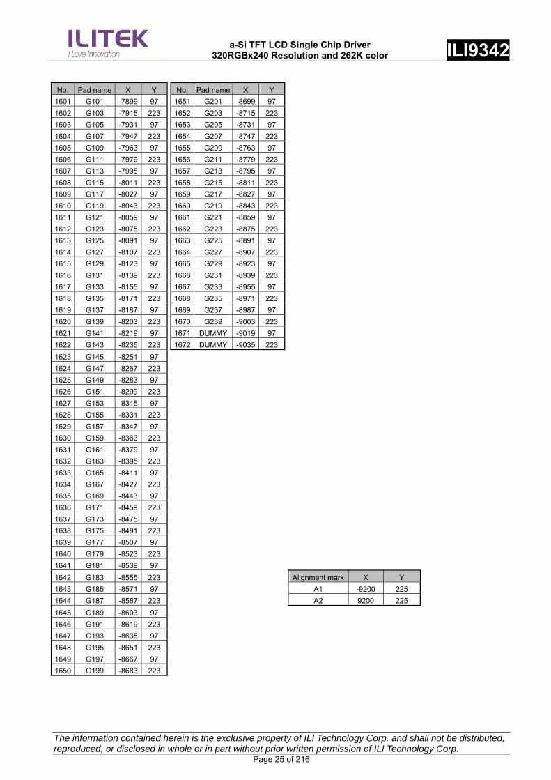
a-Si TFT LCD Single Chip Driver
320RGBx240 Resolution and 262K color ILI9342
The information contained herein is the exclusive property of ILI Technology Corp. and shall not be distributed, reproduced, or disclosed in whole or in part without prior written permission of ILI Technology Corp. Page 25 of 216
No. Pad name X Y No. Pad name X Y
1601 G101 -7899 97 1651 G201 -8699 97
1602 G103 -7915 223 1652 G203 -8715 223
1603 G105 -7931 97 1653 G205 -8731 97
1604 G107 -7947 223 1654 G207 -8747 223
1605 G109 -7963 97 1655 G209 -8763 97
1606 G111 -7979 223 1656 G211 -8779 223
1607 G113 -7995 97 1657 G213 -8795 97
1608 G115 -8011 223 1658 G215 -8811 223
1609 G117 -8027 97 1659 G217 -8827 97
1610 G119 -8043 223 1660 G219 -8843 223
1611 G121 -8059 97 1661 G221 -8859 97
1612 G123 -8075 223 1662 G223 -8875 223
1613 G125 -8091 97 1663 G225 -8891 97
1614 G127 -8107 223 1664 G227 -8907 223
1615 G129 -8123 97 1665 G229 -8923 97
1616 G131 -8139 223 1666 G231 -8939 223
1617 G133 -8155 97 1667 G233 -8955 97
1618 G135 -8171 223 1668 G235 -8971 223
1619 G137 -8187 97 1669 G237 -8987 97
1620 G139 -8203 223 1670 G239 -9003 223
1621 G141 -8219 97 1671 DUMMY -9019 97
1622 G143 -8235 223 1672 DUMMY -9035 223
1623 G145 -8251 97
1624 G147 -8267 223
1625 G149 -8283 97
1626 G151 -8299 223
1627 G153 -8315 97
1628 G155 -8331 223
1629 G157 -8347 97
1630 G159 -8363 223
1631 G161 -8379 97
1632 G163 -8395 223
1633 G165 -8411 97
1634 G167 -8427 223
1635 G169 -8443 97
1636 G171 -8459 223
1637 G173 -8475 97
1638 G175 -8491 223
1639 G177 -8507 97
1640 G179 -8523 223
1641 G181 -8539 97
1642 G183 -8555 223 Alignment mark X Y
1643 G185 -8571 97 A1 -9200 225
1644 G187 -8587 223 A2 9200 225
1645 G189 -8603 97
1646 G191 -8619 223
1647 G193 -8635 97
1648 G195 -8651 223
1649 G197 -8667 97
1650 G199 -8683 223

a-Si TFT LCD Single Chip Driver
320RGBx240 Resolution and 262K color ILI9342
The information contained herein is the exclusive property of ILI Technology Corp. and shall not be distributed, reproduced, or disclosed in whole or in part without prior written permission of ILI Technology Corp. Page 26 of 216
6.1. Bump Arrangement
Input Pad ( No.1 ~ No.436)
69
24 16 24
40Unit: um
Output Pad ( No.437 ~ No.1672)
18 14
110
161
10
Uni t: um
14
16
N o. 437 ~ No. 561N o.1549 ~ No.1672
14 14
110
161
10
Unit: um
14
14
No. 562 ~ No.1045No.1065 ~ No.1548
14 14
110
14
No.1046 ~ No.1054No.1055 ~ No.1064
Unit: um
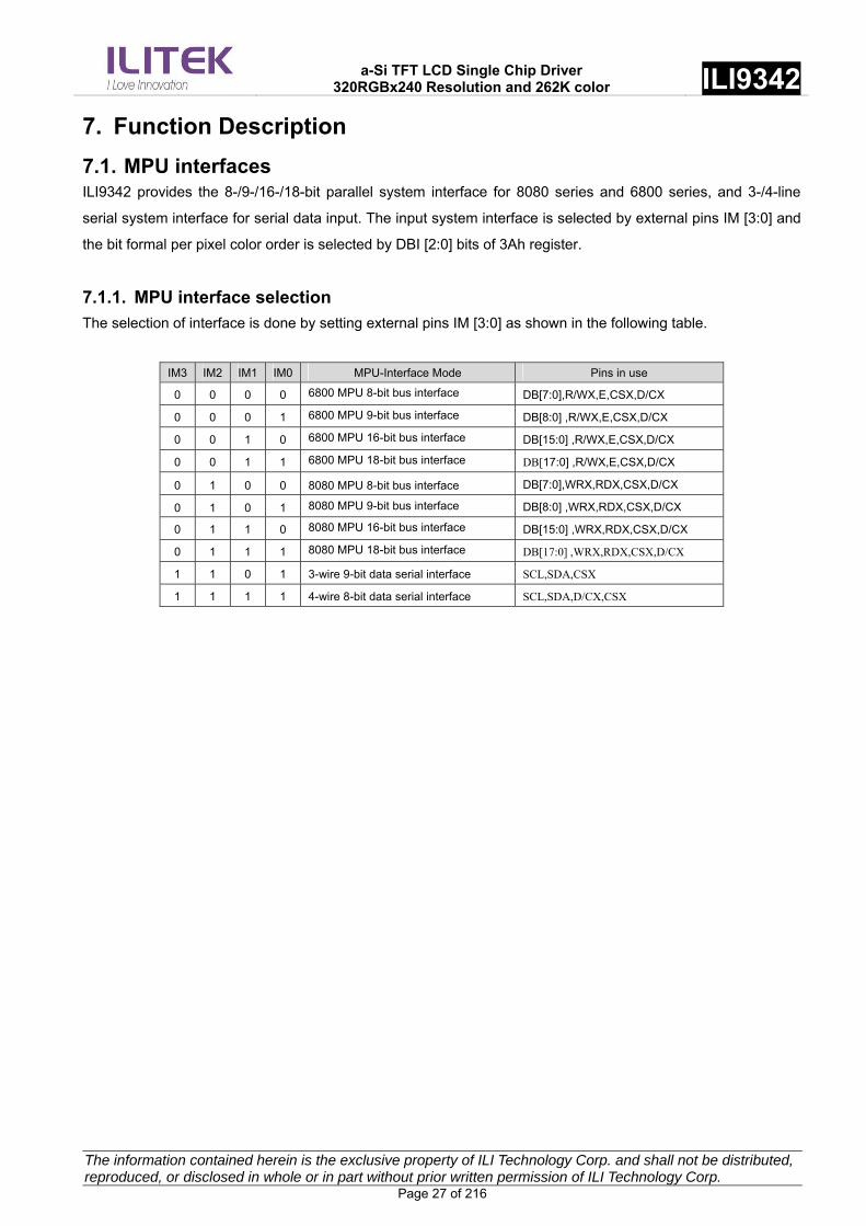
a-Si TFT LCD Single Chip Driver
320RGBx240 Resolution and 262K color ILI9342
The information contained herein is the exclusive property of ILI Technology Corp. and shall not be distributed, reproduced, or disclosed in whole or in part without prior written permission of ILI Technology Corp. Page 27 of 216
7. Function Description
7.1. MPU interfaces ILI9342 provides the 8-/9-/16-/18-bit parallel system interface for 8080 series and 6800 series, and 3-/4-line
serial system interface for serial data input. The input system interface is selected by external pins IM [3:0] and
the bit formal per pixel color order is selected by DBI [2:0] bits of 3Ah register.
7.1.1. MPU interface selection
The selection of interface is done by setting external pins IM [3:0] as shown in the following table.
IM3 IM2 IM1 IM0 MPU-Interface Mode Pins in use
0 0 0 0 6800 MPU 8-bit bus interface DB[7:0],R/WX,E,CSX,D/CX
0 0 0 1 6800 MPU 9-bit bus interface DB[8:0] ,R/WX,E,CSX,D/CX
0 0 1 0 6800 MPU 16-bit bus interface DB[15:0] ,R/WX,E,CSX,D/CX
0 0 1 1 6800 MPU 18-bit bus interface DB[17:0] ,R/WX,E,CSX,D/CX
0 1 0 0 8080 MPU 8-bit bus interface DB[7:0],WRX,RDX,CSX,D/CX
0 1 0 1 8080 MPU 9-bit bus interface DB[8:0] ,WRX,RDX,CSX,D/CX
0 1 1 0 8080 MPU 16-bit bus interface DB[15:0] ,WRX,RDX,CSX,D/CX
0 1 1 1 8080 MPU 18-bit bus interface DB[17:0] ,WRX,RDX,CSX,D/CX
1 1 0 1 3-wire 9-bit data serial interface SCL,SDA,CSX
1 1 1 1 4-wire 8-bit data serial interface SCL,SDA,D/CX,CSX
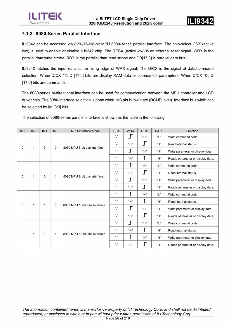
a-Si TFT LCD Single Chip Driver
320RGBx240 Resolution and 262K color ILI9342
The information contained herein is the exclusive property of ILI Technology Corp. and shall not be distributed, reproduced, or disclosed in whole or in part without prior written permission of ILI Technology Corp. Page 28 of 216
7.1.2. 8080-Series Parallel Interface
ILI9342 can be accessed via 8-/9-/16-/18-bit MPU 8080-series parallel interface. The chip-select CSX (active
low) is used to enable or disable ILI9342 chip. The RESX (active low) is an external reset signal. WRX is the
parallel data write strobe, RDX is the parallel data read strobe and DB[17:0] is parallel data bus.
ILI9342 latches the input data at the rising edge of WRX signal. The D/CX is the signal of data/command
selection. When D/CX=’1’, D [17:0] bits are display RAM data or command’s parameters. When D/CX=’0’, D
[17:0] bits are commands.
The 8080-series bi-directional interface can be used for communication between the MPU controller and LCD
driver chip. The 8080-interface selection is done when IM3 pin is low state (DGND level). Interface bus width can
be selected by IM [3:0] bits.
The selection of 8080-series parallel interface is shown as the table in the following.
IM3 IM2 IM1 IM0 MPU-Interface Mode CSX WRX RDX D/CX Function
“L” “H” “L” Write command code.
“L” “H” “H” Read internal status.
“L” “H” “H” Write parameter or display data. 0 1 0 0 8080 MPU 8-bit bus interface
“L” “H” “H” Reads parameter or display data.
“L” “H” “L” Write command code.
“L” “H” “H” Read internal status.
“L” “H” “H” Write parameter or display data. 0 1 0 1 8080 MPU 9-bit bus interface
“L” “H” “H” Reads parameter or display data.
“L” “H” “L” Write command code.
“L” “H” “H” Read internal status.
“L” “H” “H” Write parameter or display data. 0 1 1 0 8080 MPU 16-bit bus interface
“L” “H” “H” Reads parameter or display data.
“L” “H” “L” Write command code.
“L” “H” “H” Read internal status.
“L” “H” “H” Write parameter or display data. 0 1 1 1 8080 MPU 18-bit bus interface
“L” “H” “H” Reads parameter or display data.

a-Si TFT LCD Single Chip Driver
320RGBx240 Resolution and 262K color ILI9342
The information contained herein is the exclusive property of ILI Technology Corp. and shall not be distributed, reproduced, or disclosed in whole or in part without prior written permission of ILI Technology Corp. Page 29 of 216
7.1.3. Write Cycle Sequence
The WRX signal is driven from high to low and then be pulled back to high during the write cycle. The host
processor provides information during the write cycle when the display module captures the information from
host processor on the rising edge of WRX. When the D/CX signal is driven to low level, then input data on the
interface is interpreted as command information. The D/CX signal also can be pulled high level when the data on
the interface is RAM data or command’s parameter.
The following figure shows a write cycle for the 8080 MPU interface.
WRX
D[7:0], D[8:0] orD[15:0], D[17:0]
The host asserts D[17:0], D[15:0], D[8:0] or D[7:0] lines when there is falling edge of WRX
ILI9342 read D[17:0], D[15:0], D[8:0] or D[7:0] lines when there is rising edge of WRX
The host negates D[17:0], D[15:0], D[8:0] or D[7:0] lines.
Note: WRX is an unsynchronized signal (It can be stopped)
CSX
RESX
D/CX
WRX
RDX
D[17:0]
D[17:0] (LCD to Host)
CommandAddress
CommandData
Hi-Z
D[17:0] Host to LCD Command Address
Command Data
Inte
rfa
ceIL
I934
2H
ost
Signals on D[17:0], D/CX, RDX and WRX wires during CSX = "H" are ignored.
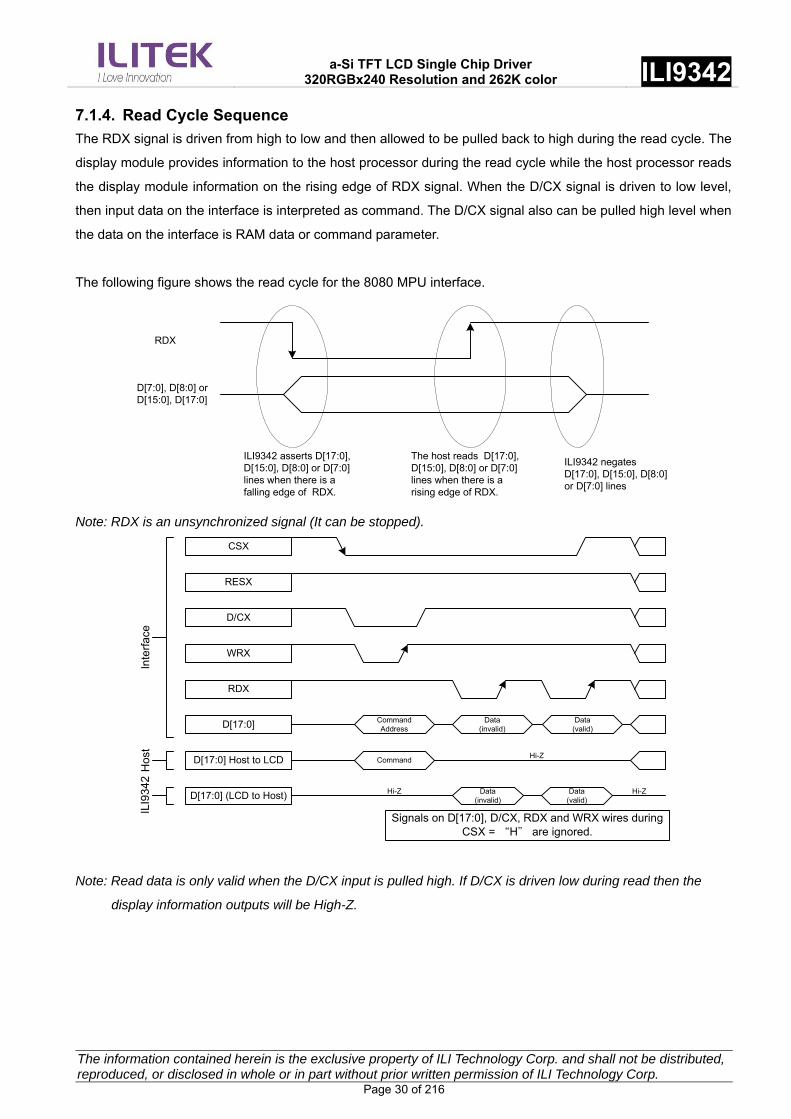
a-Si TFT LCD Single Chip Driver
320RGBx240 Resolution and 262K color ILI9342
The information contained herein is the exclusive property of ILI Technology Corp. and shall not be distributed, reproduced, or disclosed in whole or in part without prior written permission of ILI Technology Corp. Page 30 of 216
7.1.4. Read Cycle Sequence
The RDX signal is driven from high to low and then allowed to be pulled back to high during the read cycle. The
display module provides information to the host processor during the read cycle while the host processor reads
the display module information on the rising edge of RDX signal. When the D/CX signal is driven to low level,
then input data on the interface is interpreted as command. The D/CX signal also can be pulled high level when
the data on the interface is RAM data or command parameter.
The following figure shows the read cycle for the 8080 MPU interface.
RDX
D[7:0], D[8:0] orD[15:0], D[17:0]
ILI9342 asserts D[17:0], D[15:0], D[8:0] or D[7:0] lines when there is a falling edge of RDX.
The host reads D[17:0], D[15:0], D[8:0] or D[7:0] lines when there is a rising edge of RDX.
ILI9342 negates D[17:0], D[15:0], D[8:0] or D[7:0] lines
Note: RDX is an unsynchronized signal (It can be stopped).
CSX
RESX
D/CX
WRX
RDX
D[17:0] Host to LCD
D[17:0] (LCD to Host)
Command
Hi-Z Data(invalid)
Data(valid)
Hi-Z
Hi-Z
D[17:0] CommandAddress
Data(invalid)
Inte
rfac
eH
ost
ILI9
342
Data(valid)
Signals on D[17:0], D/CX, RDX and WRX wires during CSX = “H" are ignored.
Note: Read data is only valid when the D/CX input is pulled high. If D/CX is driven low during read then the
display information outputs will be High-Z.
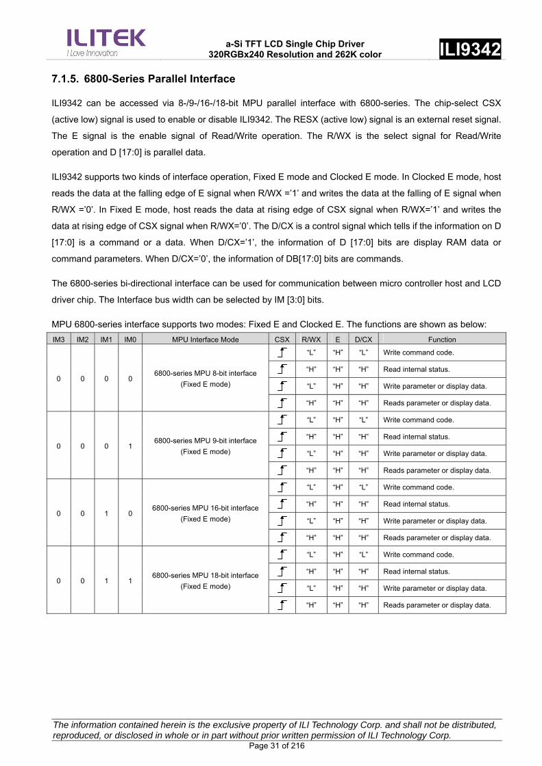
a-Si TFT LCD Single Chip Driver
320RGBx240 Resolution and 262K color ILI9342
The information contained herein is the exclusive property of ILI Technology Corp. and shall not be distributed, reproduced, or disclosed in whole or in part without prior written permission of ILI Technology Corp. Page 31 of 216
7.1.5. 6800-Series Parallel Interface
ILI9342 can be accessed via 8-/9-/16-/18-bit MPU parallel interface with 6800-series. The chip-select CSX
(active low) signal is used to enable or disable ILI9342. The RESX (active low) signal is an external reset signal.
The E signal is the enable signal of Read/Write operation. The R/WX is the select signal for Read/Write
operation and D [17:0] is parallel data.
ILI9342 supports two kinds of interface operation, Fixed E mode and Clocked E mode. In Clocked E mode, host
reads the data at the falling edge of E signal when R/WX =’1’ and writes the data at the falling of E signal when
R/WX =’0’. In Fixed E mode, host reads the data at rising edge of CSX signal when R/WX=’1’ and writes the
data at rising edge of CSX signal when R/WX=’0’. The D/CX is a control signal which tells if the information on D
[17:0] is a command or a data. When D/CX=’1’, the information of D [17:0] bits are display RAM data or
command parameters. When D/CX=’0’, the information of DB[17:0] bits are commands.
The 6800-series bi-directional interface can be used for communication between micro controller host and LCD
driver chip. The Interface bus width can be selected by IM [3:0] bits.
MPU 6800-series interface supports two modes: Fixed E and Clocked E. The functions are shown as below:
IM3 IM2 IM1 IM0 MPU Interface Mode CSX R/WX E D/CX Function
“L” “H” “L” Write command code.
“H” “H” “H” Read internal status.
“L” “H” “H” Write parameter or display data. 0 0 0 0
6800-series MPU 8-bit interface
(Fixed E mode)
“H” “H” “H” Reads parameter or display data.
“L” “H” “L” Write command code.
“H” “H” “H” Read internal status.
“L” “H” “H” Write parameter or display data. 0 0 0 1
6800-series MPU 9-bit interface
(Fixed E mode)
“H” “H” “H” Reads parameter or display data.
“L” “H” “L” Write command code.
“H” “H” “H” Read internal status.
“L” “H” “H” Write parameter or display data. 0 0 1 0
6800-series MPU 16-bit interface
(Fixed E mode)
“H” “H” “H” Reads parameter or display data.
“L” “H” “L” Write command code.
“H” “H” “H” Read internal status.
“L” “H” “H” Write parameter or display data. 0 0 1 1
6800-series MPU 18-bit interface
(Fixed E mode)
“H” “H” “H” Reads parameter or display data.

a-Si TFT LCD Single Chip Driver
320RGBx240 Resolution and 262K color ILI9342
The information contained herein is the exclusive property of ILI Technology Corp. and shall not be distributed, reproduced, or disclosed in whole or in part without prior written permission of ILI Technology Corp. Page 32 of 216
IM3 IM2 IM1 IM0 MPU Interface Mode CSX R/WX E D/CX Function
“L” “L” “L” Write command code.
“L” “H” “H” Read internal status.
“L” “L” “H” Write parameter or display data. 0 0 0 0
6800-series MPU 8-bit interface
(Clocked E mode)
“L” “H” “H” Reads parameter or display data.
“L” “L” “L” Write command code.
“L” “H” “H” Read internal status.
“L” “L” “H” Write parameter or display data. 0 0 0 1
6800-series MPU 9-bit interface
(Clocked E mode)
“L” “H” “H” Reads parameter or display data.
“L” “L” “L” Write command code.
“L” “H” “H” Read internal status.
“L” “L” “H” Write parameter or display data. 0 0 1 0
6800-series MPU 16-bit interface
(Clocked E mode)
“L” “H” “H” Reads parameter or display data.
“L” “L” “L” Write command code.
“L” “H” “H” Read internal status.
“L” “L” “H” Write parameter or display data. 0 0 1 1
6800-series MPU 18-bit interface
(Clocked E mode)
“L” “H” “H” Reads parameter or display data.

a-Si TFT LCD Single Chip Driver
320RGBx240 Resolution and 262K color ILI9342
The information contained herein is the exclusive property of ILI Technology Corp. and shall not be distributed, reproduced, or disclosed in whole or in part without prior written permission of ILI Technology Corp. Page 33 of 216
7.1.6. Write Cycle Sequence
During a write cycle, host writes commands or data to ILI9342 via the interface. The 6800-series MPU interface
supports two modes: Fixed E mode and Clocked E mode. Both modes utilize CSX, D/CX, R/WX and E signals
as well as all eight (D [7:0]), nine (D [8:0]), sixteen (D [15:0]) and eighteen (D [17:0]) information signals. D/CX is
driven to “low” while a command is present on the interface and pulled to “high” when data is on the interface.
Fixed E mode write cycle is described in the figure below.
R/WX
D[7:0], D[8:0] orD[15:0], D[17:0]
The host asserts D[17:0], D[15:0], D[8:0] or D[7:0] lines when there is falling edge of CSX
ILI9342 read D[17:0], D[15:0], D[8:0] or D[7:0] lines when there is rising edge of CSX
The host negates D[17:0], D[15:0], D[8:0] or D[7:0] lines.
CSX
E
“H"
Note: (1) E signal is tied up to “high” in Fixed E mode.
(2) CSX is unsynchronized signal (it can be stopped).
CSX
RESX
D/CX
R/WX
E
D[17:0]
D[17:0] (LCD to Host)
CommandAddress
CommandData
Hi-Z
D[17:0] Host to LCD Command Address
Command Data
Inte
rfac
eIL
I934
2H
ost

a-Si TFT LCD Single Chip Driver
320RGBx240 Resolution and 262K color ILI9342
The information contained herein is the exclusive property of ILI Technology Corp. and shall not be distributed, reproduced, or disclosed in whole or in part without prior written permission of ILI Technology Corp. Page 34 of 216
Clocked E mode write cycle is described in the figure below.
R/WX
D[7:0], D[8:0] orD[15:0], D[17:0]
The host asserts D[17:0], D[15:0], D[8:0] or D[7:0] lines when there is rising edge of E
ILI9342 read D[17:0], D[15:0], D[8:0] or D[7:0] lines when there is falling edge of E
The host negates D[17:0], D[15:0], D[8:0] or D[7:0] lines.
E
Note: (1) E is an unsynchronized signal (It can be stopped).
(2) CSX is asserted (taken low) for the same duration as the information signals.
CSX
RESX
D/CX
R/WX
E
D[17:0]
D[17:0] (LCD to Host)
CommandAddress
CommandData
Hi-Z
D[17:0] Host to LCD Command Address
Command Data
Inte
rfac
eIL
I934
2H
ost
Signals on D[17:0], D/CX, RDX and R/WX wires during CSX = “H" are ignored.
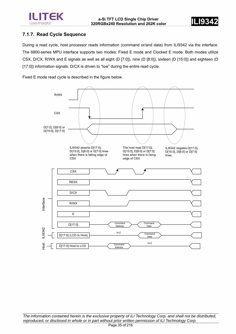
a-Si TFT LCD Single Chip Driver
320RGBx240 Resolution and 262K color ILI9342
The information contained herein is the exclusive property of ILI Technology Corp. and shall not be distributed, reproduced, or disclosed in whole or in part without prior written permission of ILI Technology Corp. Page 35 of 216
7.1.7. Read Cycle Sequence
During a read cycle, host processor reads information (command or/and data) from ILI9342 via the interface.
The 6800-series MPU interface supports two modes: Fixed E mode and Clocked E mode. Both modes utilize
CSX, D/CX, R/WX and E signals as well as all eight (D [7:0]), nine (D [8:0]), sixteen (D [15:0]) and eighteen (D
[17:0]) information signals. D/CX is driven to “low” during the entire read cycle.
Fixed E mode read cycle is described in the figure below.
D[7:0], D[8:0] orD[15:0], D[17:0]
ILI9342 asserts D[17:0], D[15:0], D[8:0] or D[7:0] lines when there is falling edge of CSX
The host read D[17:0], D[15:0], D[8:0] or D[7:0] lines when there is rising edge of CSX
ILI9342 negates D[17:0], D[15:0], D[8:0] or D[7:0] lines.
CSX
R/WX
CSX
RESX
D/CX
R/WX
E
D[17:0]
D[17:0] (LCD to Host)
CommandAddress
CommandData
Hi-Z
D[17:0] Host to LCD Command Address
Inte
rfac
eIL
I934
2H
ost
Command Data
Hi-Z

a-Si TFT LCD Single Chip Driver
320RGBx240 Resolution and 262K color ILI9342
The information contained herein is the exclusive property of ILI Technology Corp. and shall not be distributed, reproduced, or disclosed in whole or in part without prior written permission of ILI Technology Corp. Page 36 of 216
Clocked E mode write cycle is described in the figure below.
R/WX
D[7:0], D[8:0] orD[15:0], D[17:0]
ILI9342 asserts D[17:0], D[15:0], D[8:0] or D[7:0] lines when there is rising edge of E
The host read D[17:0], D[15:0], D[8:0] or D[7:0] lines when there is falling edge of E
The host negates D[17:0], D[15:0], D[8:0] or D[7:0] lines.
E
CSX
RESX
D/CX
R/WX
E
D[17:0]
D[17:0] (LCD to Host)
CommandAddress
CommandData
Hi-Z
D[17:0] Host to LCD Command Address
Inte
rfac
eIL
I934
2H
ost
Command Data
Hi-Z
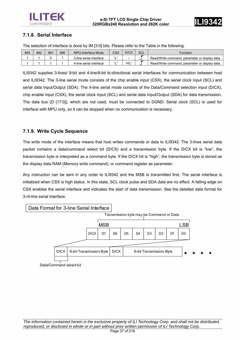
a-Si TFT LCD Single Chip Driver
320RGBx240 Resolution and 262K color ILI9342
The information contained herein is the exclusive property of ILI Technology Corp. and shall not be distributed, reproduced, or disclosed in whole or in part without prior written permission of ILI Technology Corp. Page 37 of 216
7.1.8. Serial Interface
The selection of interface is done by IM [3:0] bits. Please refer to the Table in the following.
IM3 IM2 IM1 IM0 MPU-Interface Mode CSX D/CX SCL Function
1 1 0 1 3-line serial interface “L” - Read/Write command, parameter or display data.
1 1 1 1 4-line serial interface “L” ‘H/L” Read/Write command, parameter or display data.
ILI9342 supplies 3-lines/ 9-bit and 4-line/8-bit bi-directional serial interfaces for communication between host
and ILI9342. The 3-line serial mode consists of the chip enable input (CSX), the serial clock input (SCL) and
serial data Input/Output (SDA). The 4-line serial mode consists of the Data/Command selection input (D/CX),
chip enable input (CSX), the serial clock input (SCL) and serial data Input/Output (SDA) for data transmission.
The data bus (D [17:0]), which are not used, must be connected to DGND. Serial clock (SCL) is used for
interface with MPU only, so it can be stopped when no communication is necessary.
7.1.9. Write Cycle Sequence
The write mode of the interface means that host writes commands or data to ILI9342. The 3-lines serial data
packet contains a data/command select bit (D/CX) and a transmission byte. If the D/CX bit is “low”, the
transmission byte is interpreted as a command byte. If the D/CX bit is “high”, the transmission byte is stored as
the display data RAM (Memory write command), or command register as parameter.
Any instruction can be sent in any order to ILI9342 and the MSB is transmitted first. The serial interface is
initialized when CSX is high status. In this state, SCL clock pulse and SDA data are no effect. A falling edge on
CSX enables the serial interface and indicates the start of data transmission. See the detailed data format for
3-/4-line serial interface.
D/CX D7 D6 D5 D4 D3 D2 D1 D0
MSB LSB
Transmission byte may be Command or Data
D/CX 8-bit Transmission Byte D/CX 8-bit Transmission Byte
Data/Command select bit
Data Format for 3-line Serial Interface
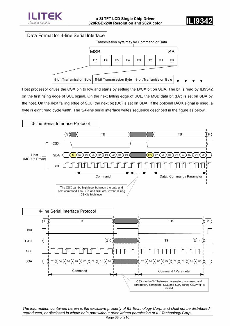
a-Si TFT LCD Single Chip Driver
320RGBx240 Resolution and 262K color ILI9342
The information contained herein is the exclusive property of ILI Technology Corp. and shall not be distributed, reproduced, or disclosed in whole or in part without prior written permission of ILI Technology Corp. Page 38 of 216
D7 D6 D5 D4 D3 D2 D1 D0
MSB LSB
Transmission byte may be Command or Data
8-bit Transmission Byte 8-bit Transmission Byte 8-bit Transmission Byte
Data Format for 4-line Serial Interface
Host processor drives the CSX pin to low and starts by setting the D/CX bit on SDA. The bit is read by ILI9342
on the first rising edge of SCL signal. On the next falling edge of SCL, the MSB data bit (D7) is set on SDA by
the host. On the next falling edge of SCL, the next bit (D6) is set on SDA. If the optional D/CX signal is used, a
byte is eight read cycle width. The 3/4-line serial interface writes sequence described in the figure as below.
S TB P
D6D7 D5 D4 D2D3 D1 D00 D6D7 D5 D4 D2D3 D1 D0D/C
TB
CSX
SDA
SCL
Command Data / Command / Parameter
The CSX can be high level between the data and next command.The SDA and SCL are invalid during
CSX is high level
Host(MCU to Driver)
3-line Serial Interface Protocol
S TB P
D6D7 D5 D4 D2D3 D6D7 D5 D4 D2D3 D1 D0
TB
CSX
D/CX
SCL
Command Command / Parameter
CSX can be "H" between parameter / command and parameter / command. SCL and SDA during CSX="H" is
invalid.
SDA
TB D/C0
D1 D0
4-line Serial Interface Protocol
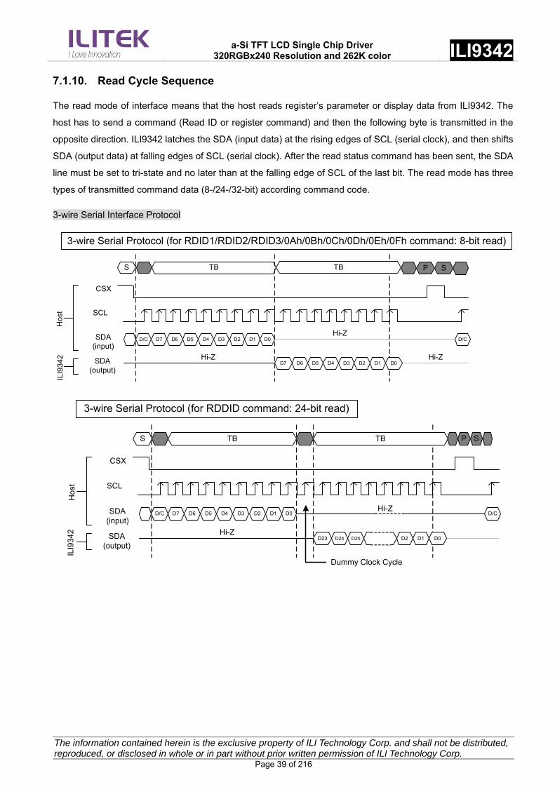
a-Si TFT LCD Single Chip Driver
320RGBx240 Resolution and 262K color ILI9342
The information contained herein is the exclusive property of ILI Technology Corp. and shall not be distributed, reproduced, or disclosed in whole or in part without prior written permission of ILI Technology Corp. Page 39 of 216
7.1.10. Read Cycle Sequence
The read mode of interface means that the host reads register’s parameter or display data from ILI9342. The
host has to send a command (Read ID or register command) and then the following byte is transmitted in the
opposite direction. ILI9342 latches the SDA (input data) at the rising edges of SCL (serial clock), and then shifts
SDA (output data) at falling edges of SCL (serial clock). After the read status command has been sent, the SDA
line must be set to tri-state and no later than at the falling edge of SCL of the last bit. The read mode has three
types of transmitted command data (8-/24-/32-bit) according command code.
3-wire Serial Interface Protocol
TB P
D6D7 D5 D4 D2D3 D1 D0D/C
D6D7 D5 D4 D2D3 D1 D0
TB
CSX
SDA(input)
SCL
Hi-Z
SS
D/C
Hi-Z Hi-Z
3-wire Serial Protocol (for RDID1/RDID2/RDID3/0Ah/0Bh/0Ch/0Dh/0Eh/0Fh command: 8-bit read)
SDA(output)
Hos
tIL
I93
42
TB P
D6D7 D5 D4 D2D3 D1 D0D/C
D24D23 D25 D2 D1 D0
TB
CSX
SDA(input)
SCL
Hi-Z
SS
D/C
Hi-ZSDA(output)
Hos
tIL
I934
2
Dummy Clock Cycle
3-wire Serial Protocol (for RDDID command: 24-bit read)
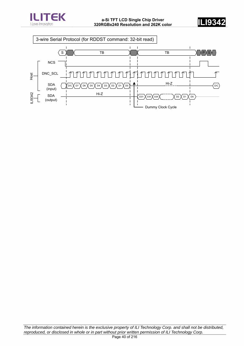
a-Si TFT LCD Single Chip Driver
320RGBx240 Resolution and 262K color ILI9342
The information contained herein is the exclusive property of ILI Technology Corp. and shall not be distributed, reproduced, or disclosed in whole or in part without prior written permission of ILI Technology Corp. Page 40 of 216
TB P
D6D7 D5 D4 D2D3 D1 D0D/C
D30D31 D29 D2 D1 D0
TB
NCS
SDA(input)
DNC_SCL
Hi-Z
SS
D/C
Hi-ZSDA(output)
Hos
tIL
I934
2
Dummy Clock Cycle
3-wire Serial Protocol (for RDDST command: 32-bit read)

a-Si TFT LCD Single Chip Driver
320RGBx240 Resolution and 262K color ILI9342
The information contained herein is the exclusive property of ILI Technology Corp. and shall not be distributed, reproduced, or disclosed in whole or in part without prior written permission of ILI Technology Corp. Page 41 of 216
4-wire Serial Interface Protocol
TB P
D6D7 D5 D4 D2D3 D1 D0
D6D7 D5 D4 D2D3 D1 D0
TB
CSX
SDA(input)
SCL
Hi-Z
SS
D7
Hi-Z
4-line Serial Protocol (for RDID1/RDID2/RDID3/0Ah/0Bh/0Ch/0Dh/0Eh/0Fh command: 8-bit read)
SDA(output)
Hos
tIL
I934
2
D/CX 0
TB P
D6D7 D5 D4 D2D3 D1 D0
D24D23 D25 D2 D1 D0
TB
CSX
SDA(input)
SCL
Hi-Z
SS
D7
Hi-ZSDA(output)
Hos
tIL
I934
2
Dummy Clock Cycle
4-line Serial Protocol (for RDDID command: 24-bit read)
0D//CX
TB P
D6D7 D5 D4 D2D3 D1 D0
D30D31 D29 D2 D1 D0
TB
CSX
SDA(input)
SCL
Hi-Z
SS
D7
Hi-ZSDA(output)
Hos
tIL
I934
2
Dummy Clock Cycle
4-line Serial Protocol (for RDDST command: 32-bit read)
0D//CX
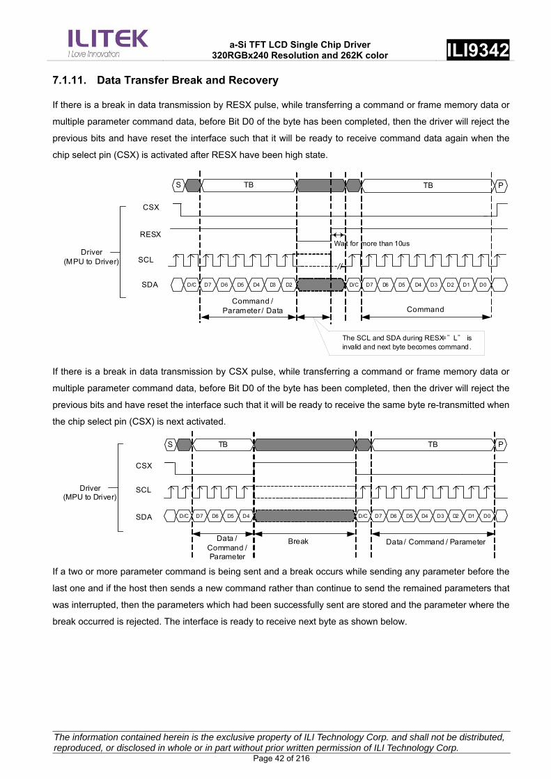
a-Si TFT LCD Single Chip Driver
320RGBx240 Resolution and 262K color ILI9342
The information contained herein is the exclusive property of ILI Technology Corp. and shall not be distributed, reproduced, or disclosed in whole or in part without prior written permission of ILI Technology Corp. Page 42 of 216
7.1.11. Data Transfer Break and Recovery
If there is a break in data transmission by RESX pulse, while transferring a command or frame memory data or
multiple parameter command data, before Bit D0 of the byte has been completed, then the driver will reject the
previous bits and have reset the interface such that it will be ready to receive command data again when the
chip select pin (CSX) is activated after RESX have been high state.
S TB P
D6D7 D5 D4 D2D3D/C D6D7 D5 D4 D2D3 D1 D0D/C
TB
CSX
RESX
SCL
Command / Parameter / Data Command
The SCL and SDA during RESX="L" is invalid and next byte becomes command.
Wait for more than 10us
SDA
Driver(MPU to Driver)
If there is a break in data transmission by CSX pulse, while transferring a command or frame memory data or
multiple parameter command data, before Bit D0 of the byte has been completed, then the driver will reject the
previous bits and have reset the interface such that it will be ready to receive the same byte re-transmitted when
the chip select pin (CSX) is next activated.
S TB P
D6D7 D5 D4D/C D6D7 D5 D4 D2D3 D1 D0D/C
TB
CSX
SDA
SCL
Break Data / Command / ParameterData /Command /Parameter
Driver(MPU to Driver)
If a two or more parameter command is being sent and a break occurs while sending any parameter before the
last one and if the host then sends a new command rather than continue to send the remained parameters that
was interrupted, then the parameters which had been successfully sent are stored and the parameter where the
break occurred is rejected. The interface is ready to receive next byte as shown below.

a-Si TFT LCD Single Chip Driver
320RGBx240 Resolution and 262K color ILI9342
The information contained herein is the exclusive property of ILI Technology Corp. and shall not be distributed, reproduced, or disclosed in whole or in part without prior written permission of ILI Technology Corp. Page 43 of 216
Command 1 Parameter 11 Parameter 12 Command 2
Command 1 Parameter 11 Parameter 13Parameter 12
BreakParameter11 is successfully sent, but Parameter12
is breaked and needed to be transfer again.
Command1 with first parameter (Parameter11) sould be excuted again to write remained parameter (Parameter12 and Parameter13)
If a two or more parameter command is being sent and a break occurs by the other command before the last
one is sent, then the parameters which had been successfully sent are stored and the other parameter of that
command remains previous value.
Command 1 Parameter 11 Command 2
Parameter 11 Parameter 13Parameter 12
Break Parameter11 is successfully sent, but other parameters are not sent and broken by the other command.
Command1 with first parameter (Parameter11) sould be excuted again to write remained parameter (Parameter12 and Parameter13)
Command 1

a-Si TFT LCD Single Chip Driver
320RGBx240 Resolution and 262K color ILI9342
The information contained herein is the exclusive property of ILI Technology Corp. and shall not be distributed, reproduced, or disclosed in whole or in part without prior written permission of ILI Technology Corp. Page 44 of 216
7.1.12. Data Transfer Pause
It will be possible when transferring a command, frame memory data or multiple parameter data to invoke a
pause in the data transmission. If the chip select pin (CSX) is released to high state after a whole byte of a frame
memory data or multiple parameter data has been completed, then ILI9342 will wait and continue the frame
memory data or parameter data transmission from the point where it was paused. If the chip select pin is
released after a whole byte of a command has been completed, then the display module will receive either the
command’s parameters (if appropriate) or a new command when the chip select pin is next enabled as shown
below.
This applies to the following 4 conditions:
1) Command-Pause-Command
2) Command-Pause-Parameter
3) Parameter-Pause-Command
4) Parameter-Pause-Parameter
Command 1
Parameter 11
Command 2 Parameter 21 Parameter 22
Pause
Condition 1:The host transmits a new Command (Command 2) when a pause occurs after Command 1.
Pause
Condition 4:The host continues to transmit the remain parameter (Parameter 22) when a pause occurs after Parameter 21.
Condition 2:The host continues to transmit the remain parameter (Parameter 11) when a pause occurs after Command 1.
Command 3
Condition 3:The host transmits a new command (Command 3) when a pause occurs after Parameter 11.
Pause
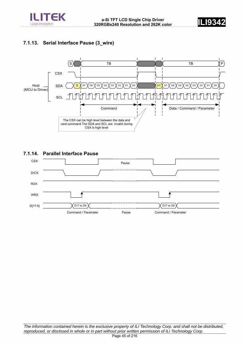
a-Si TFT LCD Single Chip Driver
320RGBx240 Resolution and 262K color ILI9342
The information contained herein is the exclusive property of ILI Technology Corp. and shall not be distributed, reproduced, or disclosed in whole or in part without prior written permission of ILI Technology Corp. Page 45 of 216
7.1.13. Serial Interface Pause (3_wire)
S TB P
D6D7 D5 D4 D2D3 D1 D00 D6D7 D5 D4 D2D3 D1 D0D/C
TB
CSX
SDA
SCL
Command Data / Command / Parameter
The CSX can be high level between the data and next command.The SDA and SCL are invalid during
CSX is high level
Host(MCU to Driver)
7.1.14. Parallel Interface Pause
D/CX
RDX
CSX
WRX
D[17:0] D17 to D0 D17 to D0
Command / Parameter Command / ParameterPause
Pause
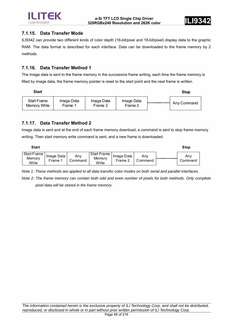
a-Si TFT LCD Single Chip Driver
320RGBx240 Resolution and 262K color ILI9342
The information contained herein is the exclusive property of ILI Technology Corp. and shall not be distributed, reproduced, or disclosed in whole or in part without prior written permission of ILI Technology Corp. Page 46 of 216
7.1.15. Data Transfer Mode
ILI9342 can provide two different kinds of color depth (16-bit/pixel and 18-bit/pixel) display data to the graphic
RAM. The data format is described for each interface. Data can be downloaded to the frame memory by 2
methods.
7.1.16. Data Transfer Method 1
The image data is sent to the frame memory in the successive frame writing, each time the frame memory is
filled by image data, the frame memory pointer is reset to the start point and the next frame is written.
Start Frame Memory Write
Image Data Frame 1
Image Data Frame 2
Image Data Frame 3
Any Command
StopStart
7.1.17. Data Transfer Method 2
Image data is sent and at the end of each frame memory download, a command is sent to stop frame memory
writing. Then start memory write command is sent, and a new frame is downloaded.
Start Frame Memory
Write
Image Data Frame 1
Any Command
Start Frame Memory
Write
Image Data Frame 2
Any Command
StopStart
Any Command
Note 1: These methods are applied to all data transfer color modes on both serial and parallel interfaces.
Note 2: The frame memory can contain both odd and even number of pixels for both methods. Only complete
pixel data will be stored in the frame memory.

a-Si TFT LCD Single Chip Driver
320RGBx240 Resolution and 262K color ILI9342
The information contained herein is the exclusive property of ILI Technology Corp. and shall not be distributed, reproduced, or disclosed in whole or in part without prior written permission of ILI Technology Corp. Page 47 of 216
7.2. RGB Interface 7.2.1. RGB Interface Selection
ILI9342 has two kinds of RGB interface and these interfaces can be selected by RCM [1:0] bits. When RCM [1:0]
bits are set to “10”, the DE mode is selected which utilizes VSYNC, HSYNC, DOTCLK, DE, D [17:0] pins; when
RCM [1:0] bits are set to “11”, the SYNC mode is selected which utilizes which utilizes VSYNC, HSYNC,
DOTCLK, D [17:0] pins.
ILI9340 supports several pixel formats that can be selected by DPI [2:0] bits of “Pixel Format Set (3Ah)” and RIM
bit of RF6h command. The selection of a given interfaces is done by setting RCM [1:0] and DPI [2:0] as show in
the following table.
RCM[1:0] RIM DPI[2:0] RGB Interface Mode RGB Mode Used Pins
1 0 0 1 1 0 18-bit RGB interface
(262K colors)
VSYNC, HSYNC, DE, DOTCLK,
DB[17:0]
1 0 0 1 0 1 16-bit RGB interface
(65K colors)
VSYNC, HSYNC, DE, DOTCLK,
DB[15:0]
1 0 1 1 1 0 6-bit RGB interface
(262K colors)
VSYNC, HSYNC, DE, DOTCLK,
DB[5:0]
1 0 1 1 0 1 6-bit RGB interface
(65K colors)
DE Mode
Valid data is determined by
the DE signal
VSYNC, HSYNC, DE, DOTCLK,
DB[5:0]
1 1 0 1 1 0 18-bit RGB interface
(262K colors)
VSYNC, HSYNC, DOTCLK,
DB[17:0]
1 1 0 1 0 1 16-bit RGB interface
(65K colors)
VSYNC, HSYNC, DOTCLK,
DB[15:0]
1 1 1 1 1 0 6-bit RGB interface
(262K colors)
VSYNC, HSYNC, DOTCLK,
DB[5:0]
1 1 1 1 0 1 6-bit RGB interface
(65K colors)
SYNC Mode
In SYNC mode, DE signal is
ignored; blanking porch is
determined by B5h command.
VSYNC, HSYNC, DOTCLK,
DB[5:0]
18-bit data bus interface (D[17:0] is used) , DPI[2:0] = 110, and RIM=0D17 D16 D15 D14 D13 D12 D11 D10 D9 D8 D7 D6 D5 D4 D3 D2 D1 D0
R[5] R[4] R[3] R[2] R[1] R[0] G[5] G[4] G[3] G[2] G[1] G[0] B[5] B[4] B[3] B[2] B[1] B[0]18bpp Frame Memory Write
D17 D5 D4 D3 D2 D1 D0
R[5] R[4] R[3] R[2] R[1] R[0] G[5] G[4] G[3] G[2] G[1] G[0] B[5] B[4] B[3] B[2] B[1] B[0]18bpp Frame Memory Write
16-bit data bus interface (D[15:0] is used) , DPI[2:0] = 101, and RIM=0
6-bit data bus interface (D[5:0] is used) , DPI[2:0] = 110, and RIM=1D5 D4 D3 D2 D1 D0D5 D4 D3 D2 D1 D0
The LSB data of red/blue color depends on the EPF[1:0] setting.
D15 D14 D13 D12 D11 D10 D9 D8 D7 D6 D5 D4 D3 D2 D1 D0
R[4] R[3] R[2] R[1] R[0] G[5] G[4] G[3] G[2] G[1] G[0] B[4] B[3] B[2] B[1] B[0]16bpp Frame Memory Write
D17 D5 D4 D3 D2 D1 D0
R[4] R[3] R[2] R[1] R[0] G[5] G[4] G[3] G[2] G[1] G[0] B[4] B[3] B[2] B[1] B[0]16bpp Frame Memory Write
6-bit data bus interface (D[5:0] is used) , DPI[2:0] = 101, and RIM=1D5 D4 D3 D2 D1 D0D5 D4 D3 D2 D1 D0
The LSB data of red/blue color depends on the EPF[1:0] setting.
Pixel clock (DOTCLK) is running all the time without stopping and used to enter VSYNC, HSYNC, DE and D
[17:0] states when there is a rising edge of the DOTCLK. The DOTCLK cannot be used as continues internal

a-Si TFT LCD Single Chip Driver
320RGBx240 Resolution and 262K color ILI9342
The information contained herein is the exclusive property of ILI Technology Corp. and shall not be distributed, reproduced, or disclosed in whole or in part without prior written permission of ILI Technology Corp. Page 48 of 216
clock for other functions of the display module. Vertical synchronization (VSYNC) is used to tell when there is
received a new frame of the display. This is low enable and its state is read to the display module by a rising
edge of the DOTCLK signal.
Horizontal synchronization (HSYNC) is used to tell when there is received a new line of the frame. This is low
enable and its state is read to the display module by a rising edge of the DOTCLK signal.
In DE mode, Data Enable (DE) is used to tell when there is received RGB information that should be transferred
on the display. This is a high enable and its state is read to the display module by a rising edge of the DOTCLK
signal. D [17:0] are used to tell what is the information of the image that is transferred on the display (When
DE= ’0’ (low) and there is a rising edge of DOTCLK). D [17:0] can be ‘0’ (low) or ‘1’ (high). These lines are read
by a rising edge of the DOTCLK signal. In SYNC mode, the valid display data in inputted in pixel unit via D [17:0]
according to HFP/HBP settings of HSYNC signal and VFP/VBP setting of VSYNC. In both RGB interface modes,
the input display data is written to GRAM first then outputs corresponding source voltage according the gray
data from GRAM.
Hsync HBP HAdr HFP
Vsy
nc
VA
dr
VF
P
(VAdr + HAdr) - Periodwhen valid display data aretransferred from host todisplay module
(Vs
yn
c + V
BP
) - Vertica
l interval w
hen n
o valid
d
ispla
y da
ta is tra
nsferre
d from
host to d
ispla
y
(Hsync + HBP) – Horizontal interval when novalid display data is sent from host to display
VFP -- Vertical interval when no valid displaydata is transferred from host to display
HF
P - H
orizonta
l interva
l wh
en no
validd
ispla
y data is se
nt from
host to
display
VB
P
Parameters Symbols Condition Min. Typ. Max. Units
Horizontal Synchronization Hsync 2 10 16 DOTCLK
Horizontal Back Porch HBP 2 20 24 DOTCLK
Horizontal Address HAdr - 320 - DOTCLK
Horizontal Front Porch HFP 2 10 16 DOTCLK
Vertical Synchronization Vsync 1 2 4 Line
Vertical Back Porch VBP 1 2 - Line
Vertical Address VAdr - 240 - Line
Vertical Front Porch VFP 3 4 - Line

a-Si TFT LCD Single Chip Driver
320RGBx240 Resolution and 262K color ILI9342
The information contained herein is the exclusive property of ILI Technology Corp. and shall not be distributed, reproduced, or disclosed in whole or in part without prior written permission of ILI Technology Corp. Page 49 of 216
Typical values are setting example when used with panel resolution 320 x 240 (LQVGA), clock frequency
5.31MHz and frame frequency about 60Hz.
Notes:
1. Vertical period (one frame) shall be equal to the sum of Vsync + VBP + VAdr + VFP.
2. Horizontal period (one line) shall be equal to the sum of Hsync + HBP + HAdr + HFP.
3. Control signals PCLK and Hsync shall be transmitted as specified at all times while valid pixels are transferred
between the host processor and the display module.
Also make sure that
(Number of PCLK per 1 line) ≥ (Number of RTN clock) x Division ratio (DIV) x (PCDIVL+PCDIVH)
Setting Example for Display Control Clock in RGB Interface Operation
Register Display operation using DPI is in synchronization with internal clock PCLKD which is generated by
dividing DOTCLK.
PCDIVH [3:0]: Number of DOTCLK during internal clock CLKD’s high period. In units of 1 clock.
PCDIVL [3:0]: Number of DOTCLK during internal clock CLKD’s low period. In units of 1 clock.
PCDIVH and PCDIVL, specifying DOTCLK’s division ratio, are determined so that difference between
PCLKD’s frequency and internal oscillation clock 678KHz is the smallest. Set PCDIVL = PCDIVH or
PCDIVL - 1. Follow the restriction (Number of PCLK in 1H) ≥ (Number of RTN clock) * (Division ratio
(DIV)) * (PCDIVL + PCDIVH).
Setting Example: To set frame frequency to 60Hz:
Internal Clock
Internal Oscillation Clock: 236KHz
DIV[1:0] = 2’b0 (x 1/1)
RTN[4:0] = 5’h10 (16 clocks)
FP = 8'h4 (4 lines), BP = 8'h2 (2 lines), NL = 6’h1D (240 lines)
236KHz/1/(240+2+4)/16 = 59.95 Hz
Frame Rate 59.95Hz
DOTCLK
HSYNC = 10 CLK
HBP = 20 CLK
HFP=10 CLK
60Hz x (2 + 240 + 4) lines x (10 + 20 + 320 + 10) clocks = 5.31MHz
DOTCLK frequency = 5.31MHz
5.31 MHz / 236KHz = 22.5 � Set PCDIVH and PCDIVL so that PCLK is divided by 22.
5.31 MHz / 22 = 241KHz
241KHz / 16 clocks / 246 lines = 61.22Hz
PCDIVH[3:0] = 4’hB (11 DOTCLK)

a-Si TFT LCD Single Chip Driver
320RGBx240 Resolution and 262K color ILI9342
The information contained herein is the exclusive property of ILI Technology Corp. and shall not be distributed, reproduced, or disclosed in whole or in part without prior written permission of ILI Technology Corp. Page 50 of 216
PCDIVL[3:0] = 4’hB (11 DOTCLK)
DOTCLK
PCLKD
PCDIVH[3:0] PCDIVL[3:0]

a-Si TFT LCD Single Chip Driver
320RGBx240 Resolution and 262K color ILI9342
The information contained herein is the exclusive property of ILI Technology Corp. and shall not be distributed, reproduced, or disclosed in whole or in part without prior written permission of ILI Technology Corp. Page 51 of 216
7.2.2. RGB Interface Timing
The timing chart of 18-/16-bit RGB interface mode is shown as below.
HSYNC
VSYNC
DOTCLK
DE
D[17:0]
Back porch
VLW> =1H
1 frame
Front porch
Valid data
HLW>=3DOTCLKs
1H
DTST>=HLW
HSYNC
DOTCLK
DE
D[17:0]
VLW : VSYNC Low WidthHLW : HSYNC Low WidthDTST : Data Transfer Startup Time
Note 1: The DE signal is not needed when RGB interface SYNC mode is selected.
Note 2: VSPL=’0’, HSPL=’0’, DPL=’0’ and EPL=’1’ of “Interface Mode Control (B0h)” command.

a-Si TFT LCD Single Chip Driver
320RGBx240 Resolution and 262K color ILI9342
The information contained herein is the exclusive property of ILI Technology Corp. and shall not be distributed, reproduced, or disclosed in whole or in part without prior written permission of ILI Technology Corp. Page 52 of 216
The timing chart of 6-bit RGB interface mode is shown as below:
HSYNC
VSYNC
DOTCLK
ENABLE
D[5:0]
Back porch
VLW>=1H
1 frame
Front porch
Valid data
HLW>=3DOTCLKs
1H
DTST>=HLW
HSYNC
DOTCLK
ENABLE
D[5:0]
VLW : VSYNC Low WidthHLW : HSYNC Low WidthDTST : Data Transfer Startup Time
R G B R G B B R G B
Note 1: The DE signal is not needed when RGB interface SYNC mode is selected.
Note 2: VSPL=’0’, HSPL=’0’, DPL=’0’ and EPL=’1’ of “Interface Mode Control (B0h)” command.
Note 3: In 6-bit RGB interface mode, each dot of one pixel (R, G and B) is transferred in synchronization with
DOTCLK.
Note 4: In 6-bit RGB interface mode, set the cycles of VSYNC, HSYNC and DE to 3 multiples of DOTCLK.

a-Si TFT LCD Single Chip Driver
320RGBx240 Resolution and 262K color ILI9342
The information contained herein is the exclusive property of ILI Technology Corp. and shall not be distributed, reproduced, or disclosed in whole or in part without prior written permission of ILI Technology Corp. Page 53 of 216
7.3. VSYNC Interface ILI9342 supports the VSYNC interface in synchronization with the frame-synchronizing signal VSYNC to display
the moving picture with the 8080/6800 system interface. When the VSYNC interface is selected to display a
moving picture, the minimum GRAM update speed is limited and the VSYNC interface is enabled by setting
DM[1:0] = “10” and RM = “0”.
MPU
VSYNC
nCS
RS
DB[17:0]
nWR
In the VSYNC mode, the display operation is synchronized with the internal clock and VSYNC input and the
frame rate is determined by the pulse rate of VSYNC signal. All display data are stored in GRAM to minimize
total data transfer required for moving picture display.
Rewritingscreen data
Rewritingscreen data
VSYNC
Write data to RAMthrough system
interface
Display operationsynchronized with
internal clocks
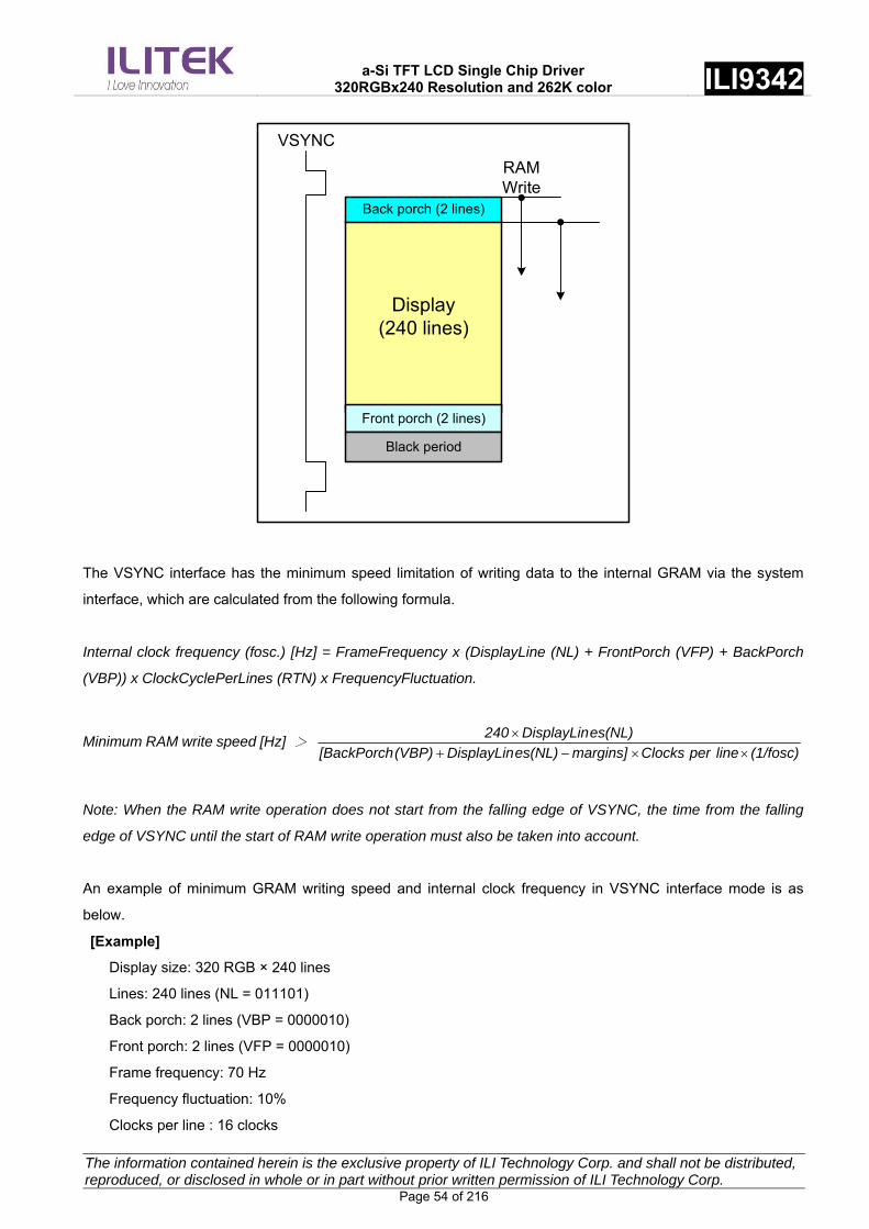
a-Si TFT LCD Single Chip Driver
320RGBx240 Resolution and 262K color ILI9342
The information contained herein is the exclusive property of ILI Technology Corp. and shall not be distributed, reproduced, or disclosed in whole or in part without prior written permission of ILI Technology Corp. Page 54 of 216
Display(240 lines)
Back porch (2 lines)
Front porch (2 lines)
Black period
VSYNC
RAMWrite
The VSYNC interface has the minimum speed limitation of writing data to the internal GRAM via the system
interface, which are calculated from the following formula.
Internal clock frequency (fosc.) [Hz] = FrameFrequency x (DisplayLine (NL) + FrontPorch (VFP) + BackPorch
(VBP)) x ClockCyclePerLines (RTN) x FrequencyFluctuation.
Minimum RAM write speed [Hz] > (1/fosc)line perClocks margins]es(NL)DisplayLin(VBP)[BackPorch
es(NL)DisplayLin240
Note: When the RAM write operation does not start from the falling edge of VSYNC, the time from the falling
edge of VSYNC until the start of RAM write operation must also be taken into account.
An example of minimum GRAM writing speed and internal clock frequency in VSYNC interface mode is as
below.
[Example]
Display size: 320 RGB × 240 lines
Lines: 240 lines (NL = 011101)
Back porch: 2 lines (VBP = 0000010)
Front porch: 2 lines (VFP = 0000010)
Frame frequency: 70 Hz
Frequency fluctuation: 10%
Clocks per line : 16 clocks

a-Si TFT LCD Single Chip Driver
320RGBx240 Resolution and 262K color ILI9342
The information contained herein is the exclusive property of ILI Technology Corp. and shall not be distributed, reproduced, or disclosed in whole or in part without prior written permission of ILI Technology Corp. Page 55 of 216
Internal oscillator clock (fosc.) [Hz] = 70 x [240+ 2 + 2] x 16 clocks x (1.1/0.9) ≒ 334KHz
When calculate the internal clock frequency, the oscillator variation is needed to be taken into consideration. In
the above example, the calculated internal clock frequency with ±10% margin variation is considered and
ensures to complete the display operation within one VSYNC cycle. The causes of frequency variation come
from fabrication process of LSI, room temperature, external resistors and VCI voltage variation.
Minimum speed for RAM writing [Hz] > 320 x 240 x 334K / [ (2 + 240 + 2)lines x 16clocks] ≒ 6.57 MHz
The above theoretical value is calculated based on the premise that the ILI9342 starts to write data into the
internal GRAM on the falling edge of VSYNC. There must at least be a margin of 2 lines between the physical
display line and the GRAM line address where data writing operation is performed. The GRAM write speed of
6.57MHz or more will guarantee the completion of GRAM write operation before the ILI9342 starts to display the
GRAM data on the screen and enable to rewrite the entire screen without flicker.
Notes in using the VSYNC interface
1. The minimum GRAM write speed must be satisfied and the frequency variation must be taken into
consideration.
2. The display frame rate is determined by the VSYNC signal and the period of VSYNC must be longer than the
scan period of an entire display.
3. When switching from the internal clock operation mode (DM[1:0] = “00”) to the VSYNC interface mode or
inversely, the switching starts from the next VSYNC cycle, i.e. after completing the display of the frame.
4. The partial display, vertical scroll, and interlaced scan functions are not available in VSYNC interface mode.

a-Si TFT LCD Single Chip Driver
320RGBx240 Resolution and 262K color ILI9342
The information contained herein is the exclusive property of ILI Technology Corp. and shall not be distributed, reproduced, or disclosed in whole or in part without prior written permission of ILI Technology Corp. Page 56 of 216
Set GRAM Address
Set DM[1:0]=10, RM=0for VSYNC interface mode
Set index register to 2Ch
Write data to GRAMthrough VSYNC interface
Wait more than 1 frame
System Interface Mode to VSYNC interface mode
System Interface
Opeartion through VSYNC interface
Display operation in synchronization with internal clocks
DM[1:0], RM become enable after completion of displaying 1 frame
Display operation in synchronization with VSYNC
Set DM[1:0]=00, RM=0for system interface mode
Wait more than 1 frame
VSYNC interface mode to System Interface Mode
System Interface
Opeartion through VSYNC interface
Display operation in synchronization with internal clocks
Display operation in synchronization with VSYNC
DM[1:0], RM become enable after completion of displaying 1 frame
Note: input VSYNC for more than 1 frame period after setting the DM, RM register.

a-Si TFT LCD Single Chip Driver
320RGBx240 Resolution and 262K color ILI9342
The information contained herein is the exclusive property of ILI Technology Corp. and shall not be distributed, reproduced, or disclosed in whole or in part without prior written permission of ILI Technology Corp. Page 57 of 216
7.4. Color Depth Conversion Look-Up Table When ILI9342 operates in parallel 16-bit interface, the color depth conversion is done by look-up table and
extend input data format to 18-bit. See the detailed for look-up table of color depth conversion.
R input (5-bit)
16-bit/pixel –mode
65,536 colors
R output (6-bit)
18-bit/pixel –mode
262,144 colors
Command Code (0x2Dh)
RGBSET Parameter
00000 R005 R004 R003 R002 R001 R000 1
00001 R015 R014 R013 R012 R011 R010 2
00010 R025 R024 R023 R022 R021 R020 3
00011 R035 R034 R033 R032 R031 R030 4
00100 R045 R044 R043 R042 R041 R040 5
00101 R055 R054 R053 R052 R051 R050 6
00110 R065 R064 R063 R062 R061 R060 7
00111 R075 R074 R073 R072 R071 R070 8
01000 R085 R084 R083 R082 R081 R080 9
01001 R095 R094 R093 R092 R091 R090 10
01010 R105 R104 R103 R102 R101 R100 11
01011 R115 R114 R113 R112 R111 R110 12
01100 R125 R124 R123 R122 R121 R120 13
01101 R135 R134 R133 R132 R131 R130 14
01110 R145 R144 R143 R142 R141 R140 15
01111 R155 R154 R153 R152 R151 R150 16
10000 R165 R164 R163 R162 R161 R160 17
10001 R175 R174 R173 R172 R171 R170 18
10010 R185 R184 R183 R182 R181 R180 19
10011 R195 R194 R193 R192 R191 R190 20
10100 R205 R204 R203 R202 R201 R200 21
10101 R215 R214 R213 R212 R211 R210 22
10110 R225 R224 R223 R222 R221 R220 23
10111 R235 R234 R233 R232 R231 R230 24
11000 R245 R244 R243 R242 R241 R240 25
11001 R255 R254 R253 R252 R251 R250 26
11010 R265 R264 R263 R262 R261 R260 27
11011 R275 R274 R273 R272 R271 R270 28
11100 R285 R284 R283 R282 R281 R280 29
11101 R295 R294 R293 R292 R291 R290 30
11110 R305 R304 R303 R302 R301 R300 31
11111 R315 R314 R313 R312 R311 R310 32
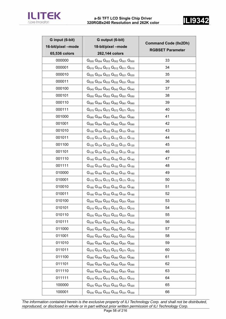
a-Si TFT LCD Single Chip Driver
320RGBx240 Resolution and 262K color ILI9342
The information contained herein is the exclusive property of ILI Technology Corp. and shall not be distributed, reproduced, or disclosed in whole or in part without prior written permission of ILI Technology Corp. Page 58 of 216
G input (6-bit)
16-bit/pixel –mode
65,536 colors
G output (6-bit)
18-bit/pixel –mode
262,144 colors
Command Code (0x2Dh)
RGBSET Parameter
000000 G005 G004 G003 G002 G001 G000 33
000001 G015 G014 G013 G012 G011 G010 34
000010 G025 G024 G023 G022 G021 G020 35
000011 G035 G034 G033 G032 G031 G030 36
000100 G045 G044 G043 G042 G041 G040 37
000101 G055 G054 G053 G052 G051 G050 38
000110 G065 G064 G063 G062 G061 G060 39
000111 G075 G074 G073 G072 G071 G070 40
001000 G085 G084 G083 G082 G081 G080 41
001001 G095 G094 G093 G092 G091 G090 42
001010 G105 G104 G103 G102 G101 G100 43
001011 G115 G114 G113 G112 G111 G110 44
001100 G125 G124 G123 G122 G121 G120 45
001101 G135 G134 G133 G132 G131 G130 46
001110 G145 G144 G143 G142 G141 G140 47
001111 G155 G154 G153 G152 G151 G150 48
010000 G165 G164 G163 G162 G161 G160 49
010001 G175 G174 G173 G172 G171 G170 50
010010 G185 G184 G183 G182 G181 G180 51
010011 G195 G194 G193 G192 G191 G190 52
010100 G205 G204 G203 G202 G201 G200 53
010101 G215 G214 G213 G212 G211 G210 54
010110 G225 G224 G223 G222 G221 G220 55
010111 G235 G234 G233 G232 G231 G230 56
011000 G245 G244 G243 G242 G241 G240 57
011001 G255 G254 G253 G252 G251 G250 58
011010 G265 G264 G263 G262 G261 G260 59
011011 G275 G274 G273 G272 G271 G270 60
011100 G285 G284 G283 G282 G281 G280 61
011101 G295 G294 G293 G292 G291 G290 62
011110 G305 G304 G303 G302 G301 G300 63
011111 G315 G314 G313 G312 G311 G310 64
100000 G325 G324 G323 G322 G321 G320 65
100001 G335 G334 G333 G332 G331 G330 66

a-Si TFT LCD Single Chip Driver
320RGBx240 Resolution and 262K color ILI9342
The information contained herein is the exclusive property of ILI Technology Corp. and shall not be distributed, reproduced, or disclosed in whole or in part without prior written permission of ILI Technology Corp. Page 59 of 216
G input (6-bit)
16-bit/pixel –mode
65,536 colors
G output (6-bit)
18-bit/pixel –mode
262,144 colors
Command Code (0x2Dh)
RGBSET Parameter
100010 G345 G344 G343 G342 G341 G340 67
100011 G355 G354 G353 G352 G351 G350 68
100100 G365 G364 G363 G362 G361 G360 69
100101 G375 G374 G373 G372 G371 G370 70
100110 G385 G384 G383 G382 G381 G380 71
100111 G395 G394 G393 G392 G391 G390 72
101000 G405 G404 G403 G402 G401 G400 73
101001 G415 G414 G413 G412 G411 G410 74
101010 G425 G424 G423 G422 G421 G420 75
101011 G435 G434 G433 G432 G431 G430 76
101100 G445 G444 G443 G442 G441 G440 77
101101 G455 G454 G453 G452 G451 G450 78
101110 G465 G464 G463 G462 G461 G460 79
101111 G475 G474 G473 G472 G471 G470 80
110000 G485 G484 G483 G482 G481 G480 81
110001 G495 G494 G493 G492 G491 G490 82
110010 G505 G504 G503 G502 G501 G500 83
110011 G515 G514 G513 G512 G511 G510 84
110100 G525 G524 G523 G522 G521 G520 85
110101 G535 G534 G533 G532 G531 G530 86
110110 G545 G544 G543 G542 G541 G540 87
110111 G555 G554 G553 G552 G551 G550 88
111000 G565 G564 G563 G562 G561 G560 89
111001 G575 G574 G573 G572 G571 G570 90
111010 G585 G584 G583 G582 G581 G580 91
111011 G595 G594 G593 G592 G591 G590 92
111100 G605 G604 G603 G602 G601 G600 93
111101 G615 G614 G613 G612 G611 G610 94
111110 G625 G624 G623 G622 G621 G620 95
111111 G635 G634 G633 G632 G631 G630 96

a-Si TFT LCD Single Chip Driver
320RGBx240 Resolution and 262K color ILI9342
The information contained herein is the exclusive property of ILI Technology Corp. and shall not be distributed, reproduced, or disclosed in whole or in part without prior written permission of ILI Technology Corp. Page 60 of 216
B input (5-bit)
16-bit/pixel –mode
65,536 colors
B output (6-bit)
18-bit/pixel –mode
262,144 colors
Command Code (0x2Dh)
RGBSET Parameter
00000 B005 B004 B003 B002 B001 B000 97
00001 B015 B014 B013 B012 B011 B010 98
00010 B025 B024 B023 B022 B021 B020 99
00011 B035 B034 B033 B032 B031 B030 100
00100 B045 B044 B043 B042 B041 B040 101
00101 B055 B054 B053 B052 B051 B050 102
00110 B065 B064 B063 B062 B061 B060 103
00111 B075 B074 B073 B072 B071 B070 104
01000 B085 B084 B083 B082 B081 B080 105
01001 B095 B094 B093 B092 B091 B090 106
01010 B105 B104 B103 B102 B101 B100 107
01011 B115 B114 B113 B112 B111 B110 108
01100 B125 B124 B123 B122 B121 B120 109
01101 B135 B134 B133 B132 B131 B130 110
01110 B145 B144 B143 B142 B141 B140 111
01111 B155 B154 B153 B152 B151 B150 112
10000 B165 B164 B163 B162 B161 B160 113
10001 B175 B174 B173 B172 B171 B170 114
10010 B185 B184 B183 B182 B181 B180 115
10011 B195 B194 B193 B192 B191 B190 116
10100 B205 B204 B203 B202 B201 B200 117
10101 B215 B214 B213 B212 B211 B210 118
10110 B225 B224 B223 B222 B221 B220 119
10111 B235 B234 B233 B232 B231 B230 120
11000 B245 B244 B243 B242 B241 B240 121
11001 B255 B254 B253 B252 B251 B250 122
11010 B265 B264 B263 B262 B261 B260 123
11011 B275 B274 B273 B272 B271 B270 124
11100 B285 B284 B283 B282 B281 B280 125
11101 B295 B294 B293 B292 B291 B290 126
11110 B305 B304 B303 B302 B301 B300 127
11111 B315 B314 B313 B312 B311 B310 128

a-Si TFT LCD Single Chip Driver
320RGBx240 Resolution and 262K color ILI9342
The information contained herein is the exclusive property of ILI Technology Corp. and shall not be distributed, reproduced, or disclosed in whole or in part without prior written permission of ILI Technology Corp. Page 61 of 216
7.5. Display Data RAM (DDRAM) ILI9342 has an integrated 320x240x18-bit graphic type static RAM. This 172,800-byte memory allows storing a
320xRGBx240 image with an 18-bit resolution (262K-color). There is no abnormal visible effect on the display
when there are simultaneous panel display read and interface read/write to the same location of the frame
memory.
MPU Look-Up Tale
Row Address Counter
Column Address Counter
Latch
Display Data RAM(320x240x18-bit)
Line Address Counter
Scan Address Counter
Display Data RAM(320x240x18-bit)

a-Si TFT LCD Single Chip Driver
320RGBx240 Resolution and 262K color ILI9342
The information contained herein is the exclusive property of ILI Technology Corp. and shall not be distributed, reproduced, or disclosed in whole or in part without prior written permission of ILI Technology Corp. Page 62 of 216
7.6. Display Data Format ILI9342 supplies 18-/16-/9-/8-bit parallel MPU interface with 8080/6800-series, 3-/4-line serial interface and
6-/16-18-bit parallel RGB interface. The parallel MPU interface and serial interface mode can be selected by
external pins IM [3:0] and RGB interface mode can be selected by software command parameters RCM[1:0].
7.6.1. 3-line Serial Interface
The 3-line/9-bit serial bus interface of ILI9342 can be used by setting external pin as IM [3:0] to “1101”. The
shown figure is the example of 3-line SPI interface.
MPU ILI9342
SCLCSXSDA
D[17:0]
In 3-line serial interface, different display data format is available for two color depths supported by the LCM
listed below.
-65k colors, RGB 5, 6, 5 -bits input
-262k colors, RGB 6, 6, 6 -bits input.
RESX
IM[3:0]IM[3:0]=1101
CSX
D8 D7 D6 D5 D4 D3 D2 D1 D0 D8 D7 D6 D5 D4 D3 D2 D1 D0 D8 D7 D6 D5 D4 D3 D2 D1 D0
Pixel n Pixel n+1
SDA
SCL
16-bit
Frame memory
1R14
R13
R12
R11
R10
G15
G14
G13
G12
G11
G10
B14
1B13
B12
B11
B10
R24
R23
R22
R21
R20
G25
G24
G23
1
Look-Up Table for 65k Colors mapping (16-bit to 18-bit)
18-bit
R1 G1 B1 R2 G2 B2 R3 G3 B3
16 bit/pixel color order (R:5-bit, G:6-bit, B:5-bit), 65,536 colors
`1'
Note 1: The pixel data with 16-bit color depth information.
Note 2: The most significant bits are: Rx4, Gx5 and Bx4.
Note 3: The least significant bits are: Rx0, Gx0 and Bx0.
Note 4: ‘-‘= Don’t care –Can be set “0” or “1”.

a-Si TFT LCD Single Chip Driver
320RGBx240 Resolution and 262K color ILI9342
The information contained herein is the exclusive property of ILI Technology Corp. and shall not be distributed, reproduced, or disclosed in whole or in part without prior written permission of ILI Technology Corp. Page 63 of 216
RESX`1'
CSX
D8 D7 D6 D5 D4 D3 D2 D1 D0 D8 D7 D6 D5 D4 D3 D2 D1 D0 D8 D7 D6 D5 D4 D3 D2 D1 D0
Pixel n
SDA
SCL
18-bit
Frame memory
1R15
R14
R13
R12
R11
R10
- -G15
G14
G13
G12
1G11
G10
- -B15
B14
B13
B12
B11
B10
- -1
R1 G1 B1 R2 G2 B2 R3 G3 B3
18 bit/pixel color order (R:6-bit, G:6-bit, B:6-bit), 262,144 colors
IM[3:0]= 1101IM[3:0]
Note 1: The pixel data with 18-bit color depth information.
Note 2: The most significant bits are: Rx5, Gx5 and Bx5.
Note 3: The least significant bits are : Rx0, Gx0 and Bx0.
Note 4: ‘-‘= Don’t care - Can be set “0” or “1”.
RESX
IM[3:0]
CSX
- 0
D23
SCL
High-ZR2Eh
D22 D21 D20 D19 D18 D17 D16 D23D2 D1 D0 D22 D21 D20 D19
9 Dummy Clock
High-ZSDA
1-Pixel data
Host
Driver
Read data through 3-line SPI mode`1'
SDA
IM[3:0]=1101
Note 1: ‘-‘= Don’t care –Can be set “0” or “1”.
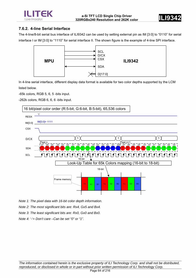
a-Si TFT LCD Single Chip Driver
320RGBx240 Resolution and 262K color ILI9342
The information contained herein is the exclusive property of ILI Technology Corp. and shall not be distributed, reproduced, or disclosed in whole or in part without prior written permission of ILI Technology Corp. Page 64 of 216
7.6.2. 4-line Serial Interface
The 4-line/8-bit serial bus interface of ILI9342 can be used by setting external pin as IM [3:0] to “0110” for serial
interface I or IM [3:0] to “1110” for serial interface II. The shown figure is the example of 4-line SPI interface.
MPU ILI9342
SCLD/CXCSX
SDA
D[17:0]
In 4-line serial interface, different display data format is available for two color depths supported by the LCM
listed below.
-65k colors, RGB 5, 6, 5 -bits input.
-262k colors, RGB 6, 6, 6 -bits input.
RESX
IM[3:0] IM[3:0]= 1111
CSX
D7 D6 D5 D4 D3 D2 D1 D0 D7 D6 D5 D4 D3 D2 D1 D0 D7 D6 D5 D4 D3 D2 D1 D0Pixel n Pixel n+1
SDA
SCL
16-bit
Frame memory
R14
R13
R12
R11
R10
G15
G14
G13
G12
G11
G10
B14
B13
B12
B11
B10
R24
R23
R22
R21
R20
G25
G24
G23
Look-Up Table for 65k Colors mapping (16-bit to 18-bit)
18-bit
R1 G1 B1 R2 G2 B2 R3 G3 B3
16 bit/pixel color order (R:5-bit, G:6-bit, B:5-bit), 65,536 colors
`1'
D7 D6 D5G22
G21
G20
D/CX 1 1 1
Note 1: The pixel data with 16-bit color depth information.
Note 2: The most significant bits are: Rx4, Gx5 and Bx4.
Note 3: The least significant bits are: Rx0, Gx0 and Bx0.
Note 4: ‘-‘= Don’t care –Can be set “0” or “1”.

a-Si TFT LCD Single Chip Driver
320RGBx240 Resolution and 262K color ILI9342
The information contained herein is the exclusive property of ILI Technology Corp. and shall not be distributed, reproduced, or disclosed in whole or in part without prior written permission of ILI Technology Corp. Page 65 of 216
RESX
CSX
D7 D6 D5 D4 D3 D2 D1 D0 D7 D6 D5 D4 D3 D2 D1 D0 D7 D6 D5 D4 D3 D2 D1 D0
Pixel n
SCL
Frame memory
R14
R13
R12
R11
R10
G15
G14
G13
G12
G10
B14
B13
B12
B11
B10
18-bit
R1 G1 B1 R2 G2 B2 R3 G3 B3
1 1D/CX
G11
R15
B15
1
`1'
IM[3:0]= 1111IM[3:0]
SDA
18 bit/pixel color order (R:6-bit, G:6-bit, B:6-bit), 262,144 colors
Note 1: The pixel data with 18-bit color depth information.
Note 2: The most significant bits are: Rx5, Gx5 and Bx5.
Note 3: The least significant bits are: Rx0, Gx0 and Bx0.
Note 4: ‘-‘= Don’t care –Can be set “0” or “1”.
RESX'
IM[3:0]
CSX
-
D23
D23
SCL
R13
R12
R11
R10
- -G15
G14
R2Eh
D22 D21 D20 D19 D18 D17 D16 D23D2 D1 D0 D22 D21 D20 D19
8 Dummy Clock
High-Z
1-Pixel data
Read Data format as below
R15
R14
D22 D21 D20 D19 D18R13
- -B15
R13
R12
D17 D16 D15 D14 D13 D12 D11 D10 D9 D8 D7 D6 D5 D4 D3 D2 D1 D0
- -R11
R10
B14
B13
B12
B11
B10
0D/CX
High-Z
Driver
Host
Read data through 4-line SPI mode
`1'
IM[3:0]=1111
SDA
SDA
Note 1: ‘-‘= Don’t care – Can be set “0” or “1”.

a-Si TFT LCD Single Chip Driver
320RGBx240 Resolution and 262K color ILI9342
The information contained herein is the exclusive property of ILI Technology Corp. and shall not be distributed, reproduced, or disclosed in whole or in part without prior written permission of ILI Technology Corp. Page 66 of 216
7.6.3. 8-bit Parallel MPU Interface
The 8080-system 8-bit parallel bus interface of ILI9640 can be used by setting external pin as IM [3:0] to “0100”.
And the 6800-system 8-bit parallel bus interface mode can be used by settings as IM [3:0] =”0000”. The figure in
the following is the example of interface with 8080/6800 microcomputer system interface.
MPU ILI9342
CSXDCXWRX (RWX)RDX (E)D[7:0]D[17:8]
Different display data formats are available for four color depths supported by listed below.
- 4K-Colors, RGB 4, 4, 4 -bits input data.
- 65K-Colors, RGB 5, 6, 5 -bits input data.
- 262K-Colors, RGB 6, 6, 6 -bits input data.

a-Si TFT LCD Single Chip Driver
320RGBx240 Resolution and 262K color ILI9342
The information contained herein is the exclusive property of ILI Technology Corp. and shall not be distributed, reproduced, or disclosed in whole or in part without prior written permission of ILI Technology Corp. Page 67 of 216
7.6.3.1. 8-bit Data Bus for 12-bit/pixel (RGB 4-4-4 bits input), 4K-color
There is 2 pixels display data per 3-bytes transfer when DBI [2:0] bits are set to “011”.
IM[3:0]
CSX
RESX
DCX
WRX
RDX
D7
D6
D5
D4
D3
D2
D1
D0
0
0
1
0
1
1
0
0
G1, Bit3
G1, Bit2
G1, Bit1
G1, Bit0
Pixel n Pixel n+1
R1
G1
B1
R2
G2
B2
R3
G3
B3
Frame Memory
B1, Bit3
B1, Bit2
B1, Bit1
B1, Bit0
R1, Bit3
R1, Bit2
R1, Bit1
R1, Bit0
G2, Bit2
G2, Bit1
G2, Bit0
`1'
`0100'/ `0000'
`1'
RWX
E
`0'
R2, Bit3
R2, Bit2
R2, Bit1
R2, Bit0
G2, Bit3
B2, Bit3
B2, Bit2
B2, Bit1
B2, Bit0
Look-Up Table for 4k Colors mapping (12-bit to 18-bit)12-bit 12-bit
18-bit 18-bit
8080-Series control pins6800-Series control pins
12 bit/pixel color order (R:4-bit, G:4-bit, B:4-bit), 4,096 colors
Note 1: The data order is as follows, MSB=D7, LSB=D0 and picture data is MSB=Bit 3, LSB=Bit 0 for Red,
Green and Blue data.
Note 2: 3-times transfer is used to transmit 2 pixel data with the 12-bits color depth information.
Note 3: ‘-‘= Don’t care – Leave these pins to Open.

a-Si TFT LCD Single Chip Driver
320RGBx240 Resolution and 262K color ILI9342
The information contained herein is the exclusive property of ILI Technology Corp. and shall not be distributed, reproduced, or disclosed in whole or in part without prior written permission of ILI Technology Corp. Page 68 of 216
7.6.3.2. 8-bit Data Bus for 16-bit/pixel (RGB 5-6-5 bits input), 65K-color
There is 1 pixel (3 sub-pixels) display data per 2-bytes transfer when DBI [2:0] bits are set to “101”.
IM[3:0 ]
CSX
RESX
DCX
WRX
RDX
D7
D6
D5
D4
D3
D2
D1
D0
0
0
1
0
1
1
0
0
R1, Bit0
G1, Bit5
G1, Bit4
G1, Bit3
Pixel n Pixel n+1
R1
G1
B1
R2
G2
B2
R3
G3
B3
Frame Memory
G1, Bit2
G1, Bit1
G1, Bit0
B1, Bit4
B2, Bit3
B2, Bit2
B2, Bit1
B2, Bit0
R1, Bit4
R1, Bit3
R1, Bit2
R1, Bit1
R2, Bit3
R2, Bit2
R2, Bit1
G2, Bit2
G2, Bit1
G2, Bit0
B2, Bit4
`1'
`0100'/ `0000'
`1'
RWX
E
`0'
B1, Bit3
B1, Bit2
B1, Bit1
B1, Bit0
R2, Bit4
R2, Bit0
G2, Bit5
G2, Bit4
G2, Bit3
Look-Up Table for 65k Colors mapping (16-bit to 18-bit)16-bit 16-bit
18-bit18-bit
8080-Series control pins6800-Series control pins
16 bit/pixel color order (R:5-bit, G:6-bit, B:5-bit), 65,536 colors
Note 1: The data order is as follows, MSB=D7, LSB=D0 and picture data is MSB=Bit 5, LSB=Bit 0 for Green data
and MSB=Bit 4, LSB=Bit0 for Red and Blue data.
Note 2: 2-times transfer is used to transmit 1 pixel data with the 16-bits color depth information.
Note 3: ‘-‘= Don’t care – Leave these pins to Open.
a-Si TFT LCD Single Chip Driver
320RGBx240 Resolution and 262K color ILI9342
The information contained herein is the exclusive property of ILI Technology Corp. and shall not be distributed, reproduced, or disclosed in whole or in part without prior written permission of ILI Technology Corp. Page 69 of 216
7.6.3.3. 8-bit Data Bus for 18-bit/pixel (RGB 6-6-6 bits input), 262K-color
There is 1 pixel (3 sub-pixels) display data per 3-bytes transfer when DBI [2:0] bits are set to “110”.
IM[3:0]
CSX
RESX
DCX
WRX
RDX
D7
D6
D5
D4
D3
D2
D1
D0
0
0
1
0
1
1
0
0
R1, Bit0
-
-
Pixel n Pixel n+1
G1, Bit5
G1, Bit4
G1, Bit3
G1, Bit2
R2, Bit1
R2, Bit0
-
-
R1, Bit4
R1, Bit3
R1, Bit2
R1, Bit1
B1, Bit4
B1, Bit3
B1, Bit2
R2, Bit5
R2, Bit4
R2, Bit3
R2, Bit2
1`'
1`'
RWX
E
`0'
G1, Bit1
G1, Bit0
-
-
B1, Bit5
B1, Bit1
B1, Bit0
-
-
18-bit 18-bit
18 bit/pixel color order (R:6-bit, G:6-bit, B:6-bit), 262,144 colors
8080-Series control pins6800-Series control pins
R1, Bit5
0`100'/ 0`000'
R1
G1
B1
R2
G2
B2
R3
G3
B3
Frame Memory
Note 1: The data order is as follows, MSB=D7, LSB=D2 and picture data is MSB=Bit 5, LSB=Bit 0 for Green,
Red and Blue data.
Note 2: 3-times transfer is used to transmit 1 pixel data with the 18-bits color depth information.
Note 3: ‘-‘= Don’t care – Leave these pins to Open.
a-Si TFT LCD Single Chip Driver
320RGBx240 Resolution and 262K color ILI9342
The information contained herein is the exclusive property of ILI Technology Corp. and shall not be distributed, reproduced, or disclosed in whole or in part without prior written permission of ILI Technology Corp. Page 70 of 216
7.6.4. 9-bit Parallel MPU Interface
The 8080-system 9-bit parallel bus interface of ILI9640 can be used by setting external pin as IM [3:0] to “0101”.
And the 6800-system 8-bit parallel bus interface mode can be used by settings as IM [3:0] =”0001”. The figure in
the following is the example of interface with 8080/6800 microcomputer system interface.
MPU ILI9342
CSXDCXWRX (RWX)RDX (E)D[8:0]D[17:9]
Display data format is available only for one color depth supported by listed below.
- 262K-Colors, RGB 6, 6, 6 -bits input data.

a-Si TFT LCD Single Chip Driver
320RGBx240 Resolution and 262K color ILI9342
The information contained herein is the exclusive property of ILI Technology Corp. and shall not be distributed, reproduced, or disclosed in whole or in part without prior written permission of ILI Technology Corp. Page 71 of 216
7.6.4.1. 9-bit Data Bus for 18-bit/pixel (RGB 6-6-6 bits input), 262K-color
There are 1 pixel (3 sub-pixels) display data per 2 transfers, when DBI [2:0] bits are set to “110”.
IM[3:0]
CSX
RESX
DCX
WRX
RDX
D7
D6
D5
D4
D3
D2
D1
D0
-
0
0
1
0
1
1
1
R1, Bit0
G1, Bit5
G1, Bit4
Pixel n Pixel n+1
R1
G1
B1
R2
G2
B2
R3
G3
B3
Frame Memory
G1, Bit2
G1, Bit1
G1, Bit0
B1, Bit5
B2, Bit4
B2, Bit3
B2, Bit2
B2, Bit1
R1, Bit4
R1, Bit3
R1, Bit2
R1, Bit1
R2, Bit4
R2, Bit3
R2, Bit2
G2, Bit2
G2, Bit1
G2, Bit0
B2, Bit5
`1'
1`'
RWX
E
0`'
B1, Bit4
B1, Bit3
B1, Bit2
B1, Bit1
R2, Bit5
R2, Bit1
R2, Bit0
G2, Bit5
G2, Bit4
18-bit 18-bit
8080-Series control pins6800-Series control pins
R1, Bit5D8
1 B1, Bit0 B2, Bit0G2, Bit3G1, Bit3
18 bit/pixel color order (R:6-bit, G:6-bit, B:6-bit), 262,144 colors
`0101'/ 0`001'
Note 1: The data order is as follows, MSB=D8, LSB=D0 and picture data is MSB=Bit 5, LSB=Bit 0 for Green,
Red and Blue data.
Note 2: 2-times transfer is used to transmit 1 pixel data with the 18-bits color depth information.
Note 3: ‘-‘= Don’t care – Leave these pins to Open.

a-Si TFT LCD Single Chip Driver
320RGBx240 Resolution and 262K color ILI9342
The information contained herein is the exclusive property of ILI Technology Corp. and shall not be distributed, reproduced, or disclosed in whole or in part without prior written permission of ILI Technology Corp. Page 72 of 216
7.6.5. 16-bit Parallel MPU Interface
The 8080-system 16-bit parallel bus interface of ILI9640 can be used by setting external pin as IM [3:0] to “0110”.
And the 6800-system 16-bit parallel bus interface mode can be used by settings as IM [3:0] =”0010”. The figure
in the following is the example of interface with 8080/6800 microcomputer system interface.
MPU ILI9342
CSXDCXWRX(RWX)RDX(E)D[15:0]D[17:16]
Different display data formats are available for four colors depth supported by listed below.
- 4K-Colors, RGB 4, 4, 4 -bits input data.
- 65K-Colors, RGB 5, 6, 5 -bits input data.
- 262K-Colors, RGB 6, 6, 6 -bits input data.

a-Si TFT LCD Single Chip Driver
320RGBx240 Resolution and 262K color ILI9342
The information contained herein is the exclusive property of ILI Technology Corp. and shall not be distributed, reproduced, or disclosed in whole or in part without prior written permission of ILI Technology Corp. Page 73 of 216
7.6.5.1. 16-bit Data Bus for 12-bit/pixel (RGB 4-4-4 bits input), 4K-color
There is 1 pixel (3 sub-pixels) display data per 2-bytes transfer when DBI [2:0] bits are set to “011”.
IM[3:0]
CSX
RESX
DCX
WRX
RDX
D7
D6
D5
D4
D3
D2
D1
D0
0
0
1
0
1
1
0
0
B1, Bit2
B1, Bit1
B1, Bit0
Pixel n Pixel n +3
R1
G1
B1
R2
G2
B2
R3
G3
B3
Frame Memory
R2, Bit0
G2, Bit3
G2, Bit2
G2, Bit1
B4, Bit3
B4, Bit2
B4, Bit1
B4, Bit0
G1, Bit3
G1, Bit2
G1, Bit1
B1, Bit3
G3, Bit3
G3, Bit2
G3, Bit1
G4, Bit0
G4, Bit3
G4, Bit2
G4, Bit1
`1'
1`'
RWX
E
0`'
B2, Bit3
B2, Bit2
B2, Bit1
B2, Bit0
R3, Bit0
B3, Bit3
B3, Bit2
B3, Bit1
B3, Bit0
12 bit/pixel color order (R:4-bit, G:4-bit, B:4-bit), 4,096 colors
8080-Series control pins6800-Series control pins
R1, Bit0
D15
D14
D13
D12
D11
D10
D9
D8
-
-
-
-
-
-
-
-
-
R1,Bit3
-
-
-
R4, Bit3
- -
-
-
R2, Bit3
-
-
-
R3, Bit3
-
Look-Up Table (12-bit to 18-bit)12-bit 12-bit
Pixel n+2Pixel n+1
18-bit 18-bit
-- - -
R2, Bit2
R2, Bit1R1, Bit1 R3, Bit1
G4, Bit2
G4, Bit1
R3, Bit2R1, Bit2
G4, Bit0g1, Bit0 G2, Bit0 G3, Bit0
0`110'/ 0`010'
Note 1: The data order is as follows, MSB=D11, LSB=D0 and picture data is MSB=Bit 3, LSB=Bit 0 for Red,
Green and Blue data.
Note 2: 1-times transfer is used to transmit 1 pixel data with the 16-bits color depth information.
Note 3: ‘-‘= Don’t care – Leave these pins to Open.

a-Si TFT LCD Single Chip Driver
320RGBx240 Resolution and 262K color ILI9342
The information contained herein is the exclusive property of ILI Technology Corp. and shall not be distributed, reproduced, or disclosed in whole or in part without prior written permission of ILI Technology Corp. Page 74 of 216
7.6.5.2. 16-bit Data Bus for 16-bit/pixel (RGB 5-6-5 bits input), 65K-color
There is 1 pixel (3 sub-pixels) display data per 2-bytes transfer when DBI [2:0] bits are set to “101”.
IM[3:0]
CSX
RESX
DCX
WRX
RDX
D7
D6
D5
D4
D3
D2
D1
D0
0
0
1
0
1
1
0
0
B1, Bit 2
B1, Bit1
B1, Bit0
Pixel n Pixel n+3
R1
G1
B1
R2
G2
B2
R3
G3
B3
Frame Memory
G2, Bit3
G2, Bit2
G2, Bit1
G2, Bit0
B4, Bit3
B4, Bit2
B4, Bit1
B4, Bit0
G1, Bit 2
G1, Bit 1
G1, Bit 0
B1, Bit3
G3, Bit 2
G3, Bit 1
G3, Bit 0
G4, Bit3
G4, Bit2
G4, Bit1
G4, Bit0
`1'
`1'
RWX
E
`0'
B2, Bit 3
B2, Bit 2
B2, Bit 1
B2, Bit 0
G3, Bit3
B3, Bit3
B3, Bit2
B3, Bit1
B3, Bit0
16 bit/pixel color order (R:5-bit, G:6-bit, B:5bit), 65,536 colors
8080-Series control pins6800-Series control pins
G1, Bit3
D15
D14
D13
D12
D11
D10
D9
D8
-
-
-
-
-
-
-
R1,Bit2
R1,Bit1
R1,Bit0
R4, Bit3
R4, Bit 2
R4, Bit1
R4, Bit0
R1, Bit3 R2, Bit3
R2, Bit2
R2, Bit1
R2, Bit0
R3, Bit3
R3, Bit2
R3, Bit1
R3, Bit0
-
Look-Up Table (16-bit to 18-bit)16-bit 16-bit
Pixel n+2Pixel n+1
18-bit 18-bit
R4, Bit 4R1, Bit4 R2, Bit4 R3, Bit4
G2, Bit5
G2, Bit4G1, Bit4 G3, Bit4
G4, Bit5
G4, Bit4
G3, Bit5G1, Bit5
B4, Bit4B1, Bit4 B2, Bit4 B3, Bit4
`0110'/ `0010'
Note 1: The data order is as follows, MSB=D15, LSB=D0 and picture data is MSB=Bit 5, LSB=Bit 0 for Green
data and MSB=Bit 4, LSB=Bit0 for Red and Blue data.
Note 2: 1-times transfer is used to transmit 1 pixel data with the 16-bits color depth information.
Note 3: ‘-‘= Don’t care – Leave these pins to Open.

a-Si TFT LCD Single Chip Driver
320RGBx240 Resolution and 262K color ILI9342
The information contained herein is the exclusive property of ILI Technology Corp. and shall not be distributed, reproduced, or disclosed in whole or in part without prior written permission of ILI Technology Corp. Page 75 of 216
7.6.5.3. 16-bit Data Bus for 18-bit/pixel (RGB 6-6-6 bits input), 262K-color
There is 1 pixel (3 sub-pixels) display data per 3-bytes transfer when DBI [2:0] bits are set to “110”.
IM[3:0]
CSX
RESX
DCX
WRX
RDX
D7
D6
D5
D4
D3
D2
D1
D0
0
0
1
0
1
1
0
0
R2, Bit3
R2, Bit2
R2, Bit1
R2, Bit0
G1, Bit2
G1, Bit1
G1, Bit0
B2, Bit 2
B2, Bit1
B2, Bit0
G3, Bit 3
G3, Bit2
G3, Bit1
G3, Bit0
`1'
`1'
RWX
E
`0'
B2, Bit3
18 bit/pixel color order (R:6-bit, G:6-bit, B:6-bit), 262,144 colors
8080-Ser ies contro l pins6800-Ser ies contro l pins
G1, Bit3
D15
D14
D13
D12
D11
D10
D9
D8
-
-
-
-
-
-
-
R1,Bit2
R1,Bit1
R1,Bit0
R3, Bit3
R3, Bit2
R3, Bit1
R3, Bit0
R1, Bit3 B1, Bit3
B1, Bit 2
B1, Bit1
B1, Bit0
G2, Bit3
G2, Bit 2
G2, Bit1
G2, Bit0
-
18-bit 18-bit
R3, Bit4R1, Bit4 B1, Bit4 G2, Bit4
R2, Bit5
R2, Bit4G1, Bit4 B2, Bit4
G3, Bit5
G3, Bit4
B2, Bit 5G1, Bit5
R3, B it5R1, Bit5 B1, Bit5 G2, Bit5
- -- -
- -- -
- -- -
- -- -
Pixel n Pixel n+1
`0110'/ ` 0010'
R1
G1
B1
R2
G2
B2
R3
G3
B3
Frame Memory
Note 1: The data order is as follows, MSB=D15, LSB=D0 and picture data is MSB=Bit 5, LSB=Bit 0 for Green,
Red and Blue data.
Note 2: 2-times transfer is used to transmit 1 pixel data with the 18-bits color depth information.
Note 3: ‘-‘= Don’t care – Leave these pins to Open.

a-Si TFT LCD Single Chip Driver
320RGBx240 Resolution and 262K color ILI9342
The information contained herein is the exclusive property of ILI Technology Corp. and shall not be distributed, reproduced, or disclosed in whole or in part without prior written permission of ILI Technology Corp. Page 76 of 216
7.6.6. 18-bit Parallel MPU Interface
The 8080-system 18-bit parallel bus interface of ILI9640 can be used by setting external pin as IM [3:0] to “0111”.
And the 6800-system 18-bit parallel bus interface mode can be used by settings as IM [3:0] =”0011”. The figure
in the following is the example of interface with 8080/6800 microcomputer system interface.
MPU ILI9342
CSXDCXWRX(RWX)RDX(E)D[17:0]
Different display data formats are available for two color depth supported by listed below.
- 262K-Colors, RGB 6, 6, 6 -bits input data.

a-Si TFT LCD Single Chip Driver
320RGBx240 Resolution and 262K color ILI9342
The information contained herein is the exclusive property of ILI Technology Corp. and shall not be distributed, reproduced, or disclosed in whole or in part without prior written permission of ILI Technology Corp. Page 77 of 216
7.6.6.1. 18-bit Data Bus for 18-bit/pixel (RGB 6-6-6 bits input), 262K-color
There is 1 pixel (3 sub-pixels) display data per 1 transfer, when DBI [2:0] bits are set to “110”
IM[3:0]
CSX
RESX
DCX
WRX
RDX
D7
D6
D5
D4
D3
D2
D1
D0
-
0
0
0
1
1
0
0
R1, Bit2
R1, Bit1
R1, Bit0
Pixel n Pixel n+3
G2, Bit3
G2, Bit2
G2, Bit1
G2, Bit0
R4, Bit3
R4, Bit2
R4, Bit1
R4, Bit0
G1, Bit2
G1, Bit1
G1, Bit0
R1, Bit3
G3, Bit2
G3, Bit1
G3, Bit0
G4, Bit3
G4, Bit2
G4, Bit1
G4, Bit0
`1'
`1'
RWX
E
`0'
R2, Bit3
R2, Bit2
R2, Bit1
R2, Bit0
G3, Bit3
R3, Bit3
R3, Bit2
R3, Bit1
R3, Bit0
8080-Series control pins6800-Series control pins
G1, Bit3
D15
D14
D13
D12
D11
D10
D9
D8
-
-
-
-
-
-
-
R1,Bit2
R1,Bit1
R1,Bit0
R4, Bit3
R4, Bit2
R4, Bit1
R4, Bit0
R1, Bit3 R2, Bit3
R2, Bit2
R2, Bit1
R2, Bit0
R3, Bit3
R3, Bit2
R3, Bit1
R3, Bit0
-
Pixel n +2Pixel n+1
18-bit 18-bit
R4, Bit4R1, Bit4 R2, Bit4 R3, Bit4
G2, Bit5
G2, Bit4G1, Bit4 G3, Bit4
G4, Bit5
G4, Bit4
G3, Bit5G1, Bit5
R4, Bit 4R1, Bit4 R2, Bit4 R3, Bit4
D16
D17 - R2, Bit5R1, Bit5 R2, Bit5 R2, Bit5
1 R4, Bit5R1, Bit5 R2, Bit5 R3, Bit5
18 bi t/pixel color order (R:6-bit, G:6-bit, B:6-bit), 262,144 colors
0`111' / `0011'
R1
G1
B1
R2
G2
B2
R3
G3
B3
Frame Memory
Note 1: The data order is as follows, MSB=D17, LSB=D0 and picture data is MSB=Bit 5, LSB=Bit 0 for Red,
Green and Blue data.
Note 2: 1-times transfer is used to transmit 1 pixel data with the 16-bits color depth information.
Note 3: ‘-‘= Don’t care – Leave these pins to Open.
a-Si TFT LCD Single Chip Driver
320RGBx240 Resolution and 262K color ILI9342
The information contained herein is the exclusive property of ILI Technology Corp. and shall not be distributed, reproduced, or disclosed in whole or in part without prior written permission of ILI Technology Corp. Page 78 of 216
7.6.7. 6-bit Parallel RGB Interface
The 6-bit RGB interface is selected by setting the DPI [2:0] bit to “110”. When RCM [1:0] are set to “10” and DE
mode is selected, the display operation is synchronized with VSYNC, HSYNC and DOTCLK signals. The
display data are transferred to the internal GRAM in synchronization with the display operation via 6-bit RGB
data bus (D [5:0]) according to the data enable signal (DE) when RCM [1:0] are set to “10”. The RGB interface
SYNC mode is selected by setting the RCM [1:0] to “11”, the valid display data is inputted in pixel unit via D [5:0]
according to the VFP/VBP and HFP/HBP settings. Unused pins must be connected to GND to ensure normally
operation. Registers can be set by the SPI system interface.
65K color: 16-bit/pixel (RGB 5-6-5 bits input)
RGB Assignment
D5 D4 D3 D2 D1 D0 D5 D4 D3 D2 D1 D0 D5 D4 D3 D2 D1 D0
1st transfer 2nd transfer 3rd transfer
R4 R3 R2 R1 R0 G5 G4 G3 G2 G1 G0 B4 B3 B2 B1 B0
Input Data
262K color: 18-bit/pixel (RGB 6-6-6 bits input)
RGB Assignment
D5 D4 D3 D2 D1 D0 D5 D4 D3 D2 D1 D0 D5 D4 D3 D2 D1 D0
1st transfer 2nd transfer 3rd transfer
R5 R4 R3 R2 R1 R0 G5 G4 G3 G2 G1 G0 B5 B4 B3 B2 B1 B0
Input Data
ILI9342 has data transfer counters to count the first, second, third data transfer in 6-bit RGB interface mode. The
transfer counter is always reset to the state of first data transfer on the falling edge of VSYNC. If a mismatch
arises in the number of each data transfer, the counter is reset to the state of first data transfer at the start of the
frame (i.e. on the falling edge of VSYNC) to restart data transfer in the correct order from the next frame. This
function is expedient for moving picture display, which requires consecutive data transfer in light of minimizing
effects from failed data transfer and enabling the system to return to a normal state.
Note that internal display operation is performed in units of pixels (RGB: taking 3 inputs of DOTCLK).
Accordingly, the number of DOTCLK inputs in one frame period must be a multiple of 3 to complete data transfer
correctly. Otherwise it will affect the display of that frame as well as the next frame.

a-Si TFT LCD Single Chip Driver
320RGBx240 Resolution and 262K color ILI9342
The information contained herein is the exclusive property of ILI Technology Corp. and shall not be distributed, reproduced, or disclosed in whole or in part without prior written permission of ILI Technology Corp. Page 79 of 216
VSYNC
HSYNC
Active Area HFPHBP
Totale Area
HSYNC
DOTCLK
D[5:0]
VBP Active Area VFP
Totale Area
SYNC Mode, RCM[1:0]=“11”
HSYNC
DOTCLK
ENABLE
VSYNC
HSYNC
ENABLE
VBP Active Area VFP
Totale Area
Active Area HFPHBP
Totale Area
D[5:0]
DE Mode, RCM[1:0]=“10”

a-Si TFT LCD Single Chip Driver
320RGBx240 Resolution and 262K color ILI9342
The information contained herein is the exclusive property of ILI Technology Corp. and shall not be distributed, reproduced, or disclosed in whole or in part without prior written permission of ILI Technology Corp. Page 80 of 216
7.6.8. 16-bit Parallel RGB Interface
The 16-bit RGB interface is selected by setting the DPI [2:0] bits to “101”. When RCM [1:0] are set to “10” and
DE mode is selected, the display operation is synchronized with VSYNC, HSYNC and DOTCLK signals. The
display data is transferred to the internal GRAM in synchronization with the display operation via 16-bit RGB
data bus (D [15:0]) according to the data enable signal (DE). The RGB interface SYNC mode is selected by
setting the RCM [1:0] to “11”, the valid display data is inputted in pixel unit via D [15:0] according to the VFP/VBP
and HFP/HBP settings. The unused D17 and D16 pins must be connected to DGND for ensure normally
operation. Registers can be set by the system interface.
R5 R4 R3 R2 R1 R0 G5 G4 G3 G2 G1 G0 B5 B4 B3 B2 B1 B0
D15 D14 D13 D12 D11 D10 D9 D8 D7 D6 D5 D4 D3 D2 D1 D0
D15 D14 D13 D12 D11 D10 D9 D8 D7 D6 D5 D4 D3 D2 D1 D0Input Data
Write Data Register
GRAM Data & RGB Mapping
Look-Up Table for 65k Colors mapping (16-bit to 18-bit)

a-Si TFT LCD Single Chip Driver
320RGBx240 Resolution and 262K color ILI9342
The information contained herein is the exclusive property of ILI Technology Corp. and shall not be distributed, reproduced, or disclosed in whole or in part without prior written permission of ILI Technology Corp. Page 81 of 216
7.6.9. 18-bit Parallel RGB Interface
The 18-bit RGB interface is selected by setting the DPI [2:0] bits to “110”. When RCM [1:0] are set to “10” and
DE mode is selected, the display operation is synchronized with VSYNC, HSYNC and DOTCLK signals. The
display data are transferred to the internal GRAM in synchronization with the display operation via 18-bit RGB
data bus (D [17:0]) according to the data enable signal (DE) when RCM [1:0] are set to “10”. The RGB interface
SYNC mode is selected by setting the RCM [1:0] to “11”, the valid display data is inputted in pixel unit via D [17:0]
according to the VFP/VBP and HFP/HBP settings. Registers can be set by the system interface.
D17 D16 D15 D14 D13 D12 D11 D10 D9 D8 D7 D6 D5 D4 D3 D2 D1 D0
R5 R4 R3 R2 R1 R0 G5 G4 G3 G2 G1 G0 B5 B4 B3 B2 B1 B0
Input Data
RGB Assignment

a-Si TFT LCD Single Chip Driver
320RGBx240 Resolution and 262K color ILI9342
The information contained herein is the exclusive property of ILI Technology Corp. and shall not be distributed, reproduced, or disclosed in whole or in part without prior written permission of ILI Technology Corp. Page 82 of 216
8. Command
8.1. Command List Regulative Command Set
Command Function D/CX RDX WRX D17-8 D7 D6 D5 D4 D3 D2 D1 D0 Hex
No Operation 0 1 ↑ XX 0 0 0 0 0 0 0 0 00h
Software Reset 0 1 ↑ XX 0 0 0 0 0 0 0 1 01h
0 1 ↑ XX 0 0 0 0 0 1 0 0 04h
1 ↑ 1 XX X X X X X X X X XX
1 ↑ 1 XX ID1 [7:0] XX
1 ↑ 1 XX ID2 [7:0] XX
Read Display Identification
Information
1 ↑ 1 XX ID3 [7:0] XX
0 1 ↑ XX 0 0 0 0 1 0 0 1 09h
1 ↑ 1 XX X X X X X X X X XX
1 ↑ 1 XX D [31:25] X 00
1 ↑ 1 XX X D [22:20] D [19:16] 61
1 ↑ 1 XX X X X X X D [10:8] 00
Read Display Status
1 ↑ 1 XX D [7:5] X X X X X 00
0 1 ↑ XX 0 0 0 0 1 0 1 0 0Ah
1 ↑ 1 XX X X X X X X X X XXRead Display Power Mode
1 ↑ 1 XX D [7:2] 0 0 08
0 1 ↑ XX 0 0 0 0 1 0 1 1 0Bh
1 ↑ 1 XX X X X X X X X X XXRead Display MADCTL
1 ↑ 1 XX D [7:2] 0 0 00
0 1 ↑ XX 0 0 0 0 1 1 0 0 0Ch
1 ↑ 1 XX X X X X X X X X XXRead Display Pixel Format
1 ↑ 1 XX RIM DPI [2:0] X DBI [2:0] 06
0 1 ↑ XX 0 0 0 0 1 1 0 1 0Dh
1 ↑ 1 XX X X X X X X X X XXRead Display Image Format
1 ↑ 1 XX X X X X X D [2:0] 00
0 1 ↑ XX 0 0 0 0 1 1 1 0 0Eh
1 ↑ 1 XX X X X X X X X X XXRead Display Signal Mode
1 ↑ 1 XX D [7:2] 0 0 00
0 1 ↑ XX 0 0 0 0 1 1 1 1 0Fh
1 ↑ 1 XX X X X X X X X X XXRead Display Self-Diagnostic
Result 1 ↑ 1 XX D [7:6] X X X X X X 00
Enter Sleep Mode 0 1 ↑ XX 0 0 0 1 0 0 0 0 10h
Sleep OUT 0 1 ↑ XX 0 0 0 1 0 0 0 1 11h
Partial Mode ON 0 1 ↑ XX 0 0 0 1 0 0 1 0 12h
Normal Display Mode ON 0 1 ↑ XX 0 0 0 1 0 0 1 1 13h
Display Inversion OFF 0 1 ↑ XX 0 0 1 0 0 0 0 0 20h
Display Inversion ON 0 1 ↑ XX 0 0 1 0 0 0 0 1 21h
0 1 ↑ XX 0 0 1 0 0 1 1 0 26hGamma Set
1 1 ↑ XX GC [7:0] 01
Display OFF 0 1 ↑ XX 0 0 1 0 1 0 0 0 28h
Display ON 0 1 ↑ XX 0 0 1 0 1 0 0 1 29h
0 1 ↑ XX 0 0 1 0 1 0 1 0 2Ah
1 1 ↑ XX SC [15:8] XX
1 1 ↑ XX SC [7:0] XX
1 1 ↑ XX EC [15:8] XX
Column Address Set
1 1 ↑ XX EC [7:0] XX
0 1 ↑ XX 0 0 1 0 1 0 1 1 2Bh
1 1 ↑ XX SP [15:8] XX
1 1 ↑ XX SP [7:0] XX
1 1 ↑ XX EP [15:8] XX
Page Address Set
1 1 ↑ XX EP [7:0] XX

a-Si TFT LCD Single Chip Driver
320RGBx240 Resolution and 262K color ILI9342
The information contained herein is the exclusive property of ILI Technology Corp. and shall not be distributed, reproduced, or disclosed in whole or in part without prior written permission of ILI Technology Corp. Page 83 of 216
0 1 ↑ XX 0 0 1 0 1 1 0 0 2ChMemory Write
1 1 ↑ D [17:0] XX
0 1 ↑ XX 0 0 1 0 1 1 0 1 2Dh
1 ↑ 1 XX R00 [5:0] XX
1 ↑ 1 XX Rnn [5:0] XX
1 ↑ 1 XX R31 [5:0] XX
1 ↑ 1 XX G00 [5:0] XX
1 ↑ 1 XX Gnn [5:0] XX
1 ↑ 1 XX G63 [5:0] XX
1 ↑ 1 XX B00 [5:0] XX
1 ↑ 1 XX Bnn [5:0] XX
Color SET
1 ↑ 1 XX B31 [5:0] XX
0 1 ↑ XX 0 0 1 0 1 1 1 0 2Eh
1 ↑ 1 XX X X X X X X X X XXMemory Read
1 ↑ 1 D [17:0] XX
0 1 ↑ XX 0 0 1 1 0 0 0 0 30h
1 1 ↑ XX SR [15:8] 00
1 1 ↑ XX SR [7:0] 00
1 1 ↑ XX ER [15:8] 00
Partial Area
1 1 ↑ XX ER [7:0] EF
0 1 ↑ XX 0 0 1 1 0 0 1 1 33h
1 1 ↑ XX TFA [15:8] 00
1 1 ↑ XX TFA [7:0] 00
1 1 ↑ XX VSA [15:8] 00
1 1 ↑ XX VSA [7:0] F0
1 1 ↑ XX BFA [15:8] 00
Vertical Scrolling Definition
1 1 ↑ XX BFA [7:0] 00
Tearing Effect Line OFF 0 1 ↑ XX 0 0 1 1 0 1 0 0 34h
0 1 ↑ XX 0 0 1 1 0 1 0 1 35hTearing Effect Line ON
1 1 ↑ XX X X X X X X X M 00
0 1 ↑ XX 0 0 1 1 0 1 1 0 36hMemory Access Control
1 1 ↑ XX MY MX MV ML BGR MH X X 00
0 1 ↑ XX 0 0 1 1 0 1 1 1 37h
1 1 ↑ XX VSP [15:8] 00Vertical Scrolling Start Address
1 1 ↑ XX VSP [7:0] 00
Idle Mode OFF 0 1 ↑ XX 0 0 1 1 1 0 0 0 38h
Idle Mode ON 0 1 ↑ XX 0 0 1 1 1 0 0 1 39h
0 1 ↑ XX 0 0 1 1 1 0 1 0 3AhPixel Format Set
1 1 ↑ XX X DPI [2:0] X DBI [2:0] 66
0 1 ↑ XX 0 0 1 1 1 1 0 0 3ChWrite Memory Continue
1 1 ↑ D [17:0] XX
0 1 ↑ XX 0 0 1 1 1 1 1 0 3Eh
1 ↑ 1 XX X X X X X X X X XXRead Memory Continue
1 ↑ 1 D [17:0] XX
0 1 ↑ XX 0 1 0 0 0 1 0 0 44h
1 1 ↑ XX X X X X X X X STS [8] 00Set Tear Scanline
1 1 ↑ XX STS [7:0] 00
0 1 ↑ XX 0 1 0 0 0 1 0 1 45h
1 ↑ 1 XX X X X X X X X X XX
1 ↑ 1 XX X X X X X X GTS [9:8] 00Get Scanline
1 ↑ 1 XX GTS [7:0] 00
0 1 ↑ XX 1 1 0 1 1 0 1 0 DAh
1 ↑ 1 XX X X X X X X X X XXRead ID1
1 ↑ 1 XX Module’s Manufacture [7:0] XX
0 1 ↑ XX 1 1 0 1 1 0 1 1 DBhRead ID2
1 ↑ 1 XX X X X X X X X X XX
a-Si TFT LCD Single Chip Driver
320RGBx240 Resolution and 262K color ILI9342
The information contained herein is the exclusive property of ILI Technology Corp. and shall not be distributed, reproduced, or disclosed in whole or in part without prior written permission of ILI Technology Corp. Page 84 of 216
1 ↑ 1 XX LCD Module / Driver Version [7:0] XX
0 1 ↑ XX 1 1 0 1 1 1 0 0 DCh
1 ↑ 1 XX X X X X X X X X XXRead ID3
1 ↑ 1 XX LCD Module / Driver ID [7:0] XX
Extended Command Set
Command Function D/CX RDX WRX D17-8 D7 D6 D5 D4 D3 D2 D1 D0 Hex
0 1 ↑ XX 1 0 1 1 0 0 0 0 B0hRGB Interface
Signal Control 1 1 ↑ XX BYPASS RCM [1:0] X VSPL HSPL DPL EPL 40
0 1 ↑ XX 1 0 1 1 0 0 0 1 B1h
1 1 ↑ XX X X X X X X DIVA [1:0] 00 Display Waveform Cycle 1
(In Normal Mode) 1 1 ↑ XX X X X RTNA [4:0] 1B
0 1 ↑ XX 1 0 1 1 0 0 1 0 B2h
1 1 ↑ XX X X X X X X DIVB [1:0] 00 Display Waveform Cycle 2
(In Idle Mode) 1 1 ↑ XX X X X RTNB [4:0] 1B
0 1 ↑ XX 1 0 1 1 0 0 1 1 B3h
1 1 ↑ XX X X X X X X DIVC [1:0] 00 Display Waveform Cycle 3
(In Partial Mode) 1 1 ↑ XX X X X RTNC [4:0] 1B
0 1 ↑ XX 1 0 1 1 0 1 0 0 B4h
1 1 ↑ XX X X X X X NLA NLB NLC 02 Display Inversion Control
1 1 ↑ XX X X NW [5:0] 00
0 1 ↑ XX 1 0 1 1 0 1 0 1 B5h
1 1 ↑ XX 0 VFP [6:0] 02
1 1 ↑ XX 0 VBP [6:0] 02
1 1 ↑ XX 0 0 0 HFP [4:0] 0A
Blanking Porch Control
1 1 ↑ XX 0 0 0 HBP [4:0] 14
0 1 ↑ XX 1 0 1 1 0 1 1 0 B6h
1 1 ↑ XX X X X X PTG [1:0] PT [1:0] 0A
1 1 ↑ XX REV GS SS SM ISC [3:0] 02
1 1 ↑ XX X X NL [5:0] 1D
Display Function Control
1 1 ↑ XX X X PCDIV[5:0] 04
0 1 ↑ XX 1 0 1 1 0 1 1 1 B7hEntry Mode Set
1 1 ↑ XX X X X X DSTB GON DTE GAS 06
0 1 ↑ XX 1 0 1 1 1 0 0 0 B8hOscillator Control
1 1 ↑ XX X X X X FOSC[3:0} 07
0 1 ↑ XX 1 0 1 1 1 0 0 0 B9h
0 1 ↑ XX EXTC1[7:0] 00
0 1 ↑ XX EXTC2[7:0] 00 Set EXTC
0 1 ↑ XX EXTC3[7:0] 00
0 1 ↑ XX 1 1 0 0 0 0 0 0 C0h
1 1 ↑ XX X X VRH [5:0] 26 Power Control 1
1 1 ↑ XX X X X X VC [3:0] 09
0 1 ↑ XX 1 1 0 0 0 0 0 1 C1hPower Control 2
1 1 ↑ XX X SAP [2:0] BT [3:0] 10
0 1 ↑ XX 1 1 0 0 0 0 1 0 C2hPower Control 3
(For Normal Mode) 1 1 ↑ XX X DCA1 [2:0] X DCA0 [2:0] C2
0 1 ↑ XX 1 1 0 0 0 0 1 1 C3hPower Control 4
(For Idle Mode) 1 1 ↑ XX X DCB1 [2:0] X DCB0 [2:0] C2
0 1 ↑ XX 1 1 0 0 0 1 0 0 C4hPower Control 5
(For Partial Mode) 1 1 ↑ XX X DCC1 [2:0] X DCC0 [2:0] C2
0 1 ↑ XX 1 1 0 0 0 1 0 1 C5h
1 1 ↑ XX X VMH [6:0] 31 VCOM Control 1
1 1 ↑ XX X VML [6:0] 3C
0 1 ↑ XX 1 1 0 0 0 1 1 1 C7hVCOM Control 2
1 1 ↑ XX nVM VMF [6:0] C0
NV Memory Write 0 1 ↑ XX 1 1 0 1 0 0 0 0 D0h

a-Si TFT LCD Single Chip Driver
320RGBx240 Resolution and 262K color ILI9342
The information contained herein is the exclusive property of ILI Technology Corp. and shall not be distributed, reproduced, or disclosed in whole or in part without prior written permission of ILI Technology Corp. Page 85 of 216
1 1 ↑ XX X X X X X PGM_ADR [2:0] 00
1 1 ↑ XX PGM_DATA [7:0] XX
0 1 ↑ XX 1 1 0 1 0 0 0 1 D1h
1 1 ↑ XX KEY [23:16] XX
1 1 ↑ XX KEY [15:8] XXNV Memory Protection Key
1 1 ↑ XX KEY [7:0] XX
0 1 ↑ XX 1 1 0 1 0 0 1 0 D2h
1 ↑ 1 XX X X X X X X X X XX
1 ↑ 1 XX X ID2_CNT [2:0] X ID1_CNT [2:0] XXNV Memory Status Read
1 ↑ 1 XX BUSY VMF_CNT [2:0] X ID3_CNT [2:0] XX
0 ↑ 1 XX 1 1 0 1 0 0 1 1 D3h
1 ↑ 1 XX X X X X X X X X XX
1 ↑ 1 XX 0 0 0 0 0 0 0 0 00
1 ↑ 1 XX 1 0 0 1 0 0 1 1 93
Read ID4
1 ↑ 1 XX 0 1 0 0 0 0 1 0 42
0 1 ↑ XX 1 1 1 0 0 0 0 0 E0h
1 1 ↑ XX X X X x VP63 [3:0] XX
1 1 ↑ XX X X VP62 [5:0] XX
1 1 ↑ XX X X VP61 [5:0] XX
1 1 ↑ XX X X X X VP59 [3:0] XX
1 1 ↑ XX X X X VP57 [4:0] XX
1 1 ↑ XX X X X X VP50 [3:0] XX
1 1 ↑ XX X VP20 [6:0] XX
1 1 ↑ XX VP36 [3:0] VP27 [3:0] XX
1 1 ↑ XX X VP20 [6:0] XX
1 1 ↑ XX X X X X VP13[3:0] XX
1 1 ↑ XX X X X VP6 [4:0] XX
1 1 ↑ XX X X X X VP4 [3:0] XX
1 1 ↑ XX X X VP2 [5:0] XX
1 1 ↑ XX X X VP1 [5:0] XX
Positive Gamma
Correction
1 1 ↑ XX X X X X VP0 [3:0] XX
0 1 ↑ XX 1 1 1 0 0 0 0 1 E1h
1 1 ↑ XX X X X X VN63 [3:0] 00
1 1 ↑ XX X X VN62 [5:0] 23
1 1 ↑ XX X X VN61 [5:0] 26
1 1 ↑ XX X X X X VN59 [3:0] 05
1 1 ↑ XX X X X VN57 [4:0] 10
1 1 ↑ XX X X X X VN50 [3:0] 04
1 1 ↑ XX X VN43 [6:0] 39
1 1 ↑ XX VN36 [3:0] VN27 [3:0] 24
1 1 ↑ XX X VN20 [6:0] 4B
1 1 ↑ XX X X X X VN13 [3:0] 03
1 1 ↑ XX X X X VN6 [4:0] 0B
1 1 ↑ XX X X X X VN4 [3:0] 0B
1 1 ↑ XX X X VN2 [5:0] 33
1 1 ↑ XX X X VN1 [5:0] 37
Negative Gamma
Correction
1 1 ↑ XX X X X x VN0 [3:0] 0F
0 1 ↑ XX 1 1 1 0 0 0 1 0 E2h
1 1 ↑ XX RCA0 [3:0] BCA0 [3:0] XX
1 1 ↑ XX RCAx [3:0] BCAx [3:0] XXDigital Gamma Control 1
1 1 ↑ XX RCA15 [3:0] BCA15 [3:0] XX
0 1 ↑ XX 1 1 1 0 0 0 1 1 E3h
1 1 ↑ XX RFA0 [3:0] BFA0 [3:0] XX
1 1 ↑ XX RFAx [3:0] BFAx [3:0] XXDigital Gamma Control 2
1 1 ↑ XX RFA63 [3:0] BFA63 [3:0] XX
Interface Control 0 1 ↑ XX 1 1 1 1 0 1 1 0 F6h

a-Si TFT LCD Single Chip Driver
320RGBx240 Resolution and 262K color ILI9342
The information contained herein is the exclusive property of ILI Technology Corp. and shall not be distributed, reproduced, or disclosed in whole or in part without prior written permission of ILI Technology Corp. Page 86 of 216
1 1 ↑ XX MY_E
OR
MX_E
OR
MV_E
ORX
BGR_
EOR X X
WEMO
DE 01
1 1 ↑ XX X X EPF [1:0] X X X X 00
1 1 ↑ XX X X EN
DIANX DM [1:0] RM RIM 00
0 1 ↑ XX 1 1 1 1 0 1 1 1 F7h
1 ↑ 1 XX X X X X X X X X XXGet GPIO0~7 Status
1 ↑ 1 XX GPI [7:0] 00
0 1 ↑ XX 1 1 1 1 1 0 0 0 F8h
0 1 ↑ XX GPO[7:0] 00 Set GPIO0~7 Status
0 1 ↑ XX IE OEB 00
Note 1: Undefined commands are treated as NOP (00h) command.
Note 2: B0 to D9 and DE to FF are for factory use of display supplier. USER can decide if these commands are
available or they are treated as NOP (00h) commands before shipping to USER. Default value is NOP
(00h).
Note 3: Commands 10h, 12h, 13h, 26h, 28h, 29h, 30h, 36h (Bit B4 only), 38h and 39h are updated during
V-SYNC when ILI9342 is in Sleep OUT mode to avoid abnormal visual effects. During Sleep IN mode,
these commands are updated immediately. Read status (09h), Read display power mode (0Ah), Read
display MADCTL (0Bh), Read display pixel format (0Ch), Read display image mode (0Dh), Read display
signal mode (0Eh) and Read display self diagnostic result (0Fh) of these commands are updated
immediately both in Sleep IN mode and Sleep OUT mode.

a-Si TFT LCD Single Chip Driver
320RGBx240 Resolution and 262K color ILI9342
The information contained herein is the exclusive property of ILI Technology Corp. and shall not be distributed, reproduced, or disclosed in whole or in part without prior written permission of ILI Technology Corp. Page 87 of 216
8.2. Description of Regulative Command Set
8.2.1. NOP (00h)
00h NOP (No Operation)
D/CX RDX WRX D17-8 D7 D6 D5 D4 D3 D2 D1 D0 HEX
Command 0 1 ↑ XX 0 0 0 0 0 0 0 0 00h
Parameter No Parameter.
Description
This command is an empty command; it does not have any effect on the display module. However it can be used to terminate
Frame Memory Write or Read as described in RAMWR (Memory Write) and RAMRD (Memory Read) Commands.
X = Don’t care.
Restriction None
Register
Availability
Status Availability
Normal Mode On, Idle Mode Off, Sleep Out Yes
Normal Mode On, Idle Mode On, Sleep Out Yes
Partial Mode On, Idle Mode Off, Sleep Out Yes
Partial Mode On, Idle Mode On, Sleep Out Yes
Sleep In Yes
Default
Status Default Value
Power On Sequence N/A
SW Reset N/A
HW Reset N/A
Flow Chart None

a-Si TFT LCD Single Chip Driver
320RGBx240 Resolution and 262K color ILI9342
The information contained herein is the exclusive property of ILI Technology Corp. and shall not be distributed, reproduced, or disclosed in whole or in part without prior written permission of ILI Technology Corp. Page 88 of 216
8.2.2. Software Reset (01h)
01h SWRESET
D/CX RDX WRX D17-8 D7 D6 D5 D4 D3 D2 D1 D0 HEX
Command 0 1 ↑ XX 0 0 0 0 0 0 0 1 01h
Parameter No Parameter.
Description
When the Software Reset command is written, it causes a software reset. It resets the commands and parameters to their
S/W Reset default values. (See default tables in each command description.)
Note: The Frame Memory contents are unaffected by this command
X = Don’t care.
Restriction
It will be necessary to wait 5msec before sending new command following software reset. The display module loads all
display supplier factory default values to the registers during this 5msec. If Software Reset is applied during Sleep Out mode,
it will be necessary to wait 120msec before sending Sleep out command. Software Reset Command cannot be sent during
Sleep Out sequence.
Register
Availability
Status Availability
Normal Mode On, Idle Mode Off, Sleep Out Yes
Normal Mode On, Idle Mode On, Sleep Out Yes
Partial Mode On, Idle Mode Off, Sleep Out Yes
Partial Mode On, Idle Mode On, Sleep Out Yes
Sleep In Yes
Default
Status Default Value
Power On Sequence N/A
SW Reset N/A
HW Reset N/A
Flow Chart
SWRESET(01h)
Display whole blank screen
Set Commands to S/W Default
Values
Sleep In Mode
Command
Parameter
Action
Mode
Legend
Sequential transfer
Display
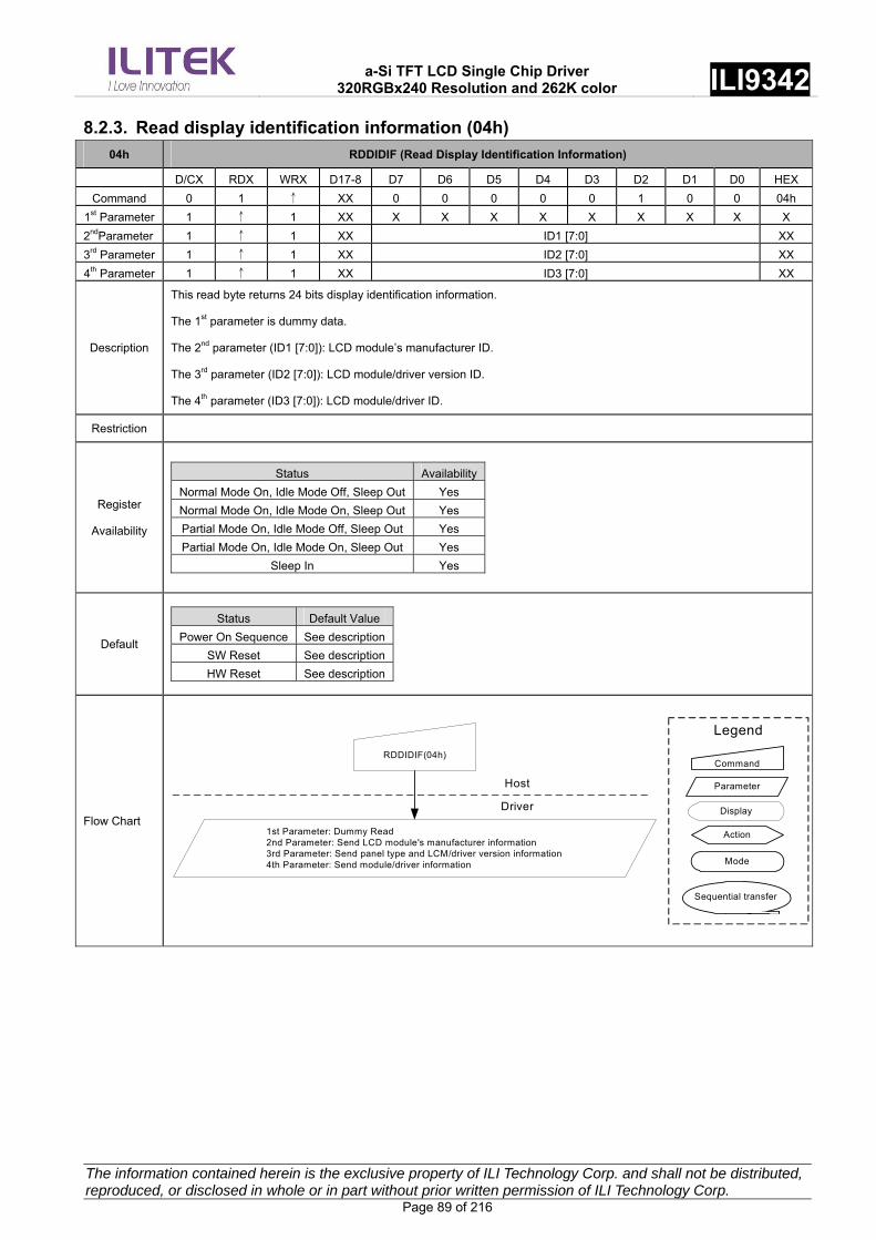
a-Si TFT LCD Single Chip Driver
320RGBx240 Resolution and 262K color ILI9342
The information contained herein is the exclusive property of ILI Technology Corp. and shall not be distributed, reproduced, or disclosed in whole or in part without prior written permission of ILI Technology Corp. Page 89 of 216
8.2.3. Read display identification information (04h)
04h RDDIDIF (Read Display Identification Information)
D/CX RDX WRX D17-8 D7 D6 D5 D4 D3 D2 D1 D0 HEX
Command 0 1 ↑ XX 0 0 0 0 0 1 0 0 04h
1st Parameter 1 ↑ 1 XX X X X X X X X X X
2ndParameter 1 ↑ 1 XX ID1 [7:0] XX
3rd Parameter 1 ↑ 1 XX ID2 [7:0] XX
4th Parameter 1 ↑ 1 XX ID3 [7:0] XX
Description
This read byte returns 24 bits display identification information.
The 1st parameter is dummy data.
The 2nd parameter (ID1 [7:0]): LCD module’s manufacturer ID.
The 3rd parameter (ID2 [7:0]): LCD module/driver version ID.
The 4th parameter (ID3 [7:0]): LCD module/driver ID.
Restriction
Register
Availability
Status Availability
Normal Mode On, Idle Mode Off, Sleep Out Yes
Normal Mode On, Idle Mode On, Sleep Out Yes
Partial Mode On, Idle Mode Off, Sleep Out Yes
Partial Mode On, Idle Mode On, Sleep Out Yes
Sleep In Yes
Default
Status Default Value
Power On Sequence See description
SW Reset See description
HW Reset See description
Flow Chart
Command
Parameter
Action
Mode
Legend
Sequential transfer
RDDIDIF(04h)
1st Parameter: Dummy Read2nd Parameter: Send LCD module's manufacturer information3rd Parameter: Send panel type and LCM/driver version information4th Parameter: Send module/driver information
Host
Driver Display

a-Si TFT LCD Single Chip Driver
320RGBx240 Resolution and 262K color ILI9342
The information contained herein is the exclusive property of ILI Technology Corp. and shall not be distributed, reproduced, or disclosed in whole or in part without prior written permission of ILI Technology Corp. Page 90 of 216
8.2.4. Read Display Status (09h) 09h RDDST (Read Display Status)
D/CX RDX WRX D17-8 D7 D6 D5 D4 D3 D2 D1 D0 HEX
Command 0 1 ↑ XX 0 0 0 0 1 0 0 1 09h
1st Parameter 1 ↑ 1 XX X X X X X X X X X
2ndParameter 1 ↑ 1 XX D [31:25] 0 00
3rdParameter 1 ↑ 1 XX 0 D [22:20] D [19:16] 61
4thParameter 1 ↑ 1 XX D15 0 D13 0 0 D [10:8] 00
5thParameter 1 ↑ 1 XX D [7:5] 0 0 0 0 0 00
Description
This command indicates the current status of the display as described in the table below:
Bit Description Value Status
0 Booster OFF D31 Booster voltage status
1 Booster ON
0 Top to Bottom (When MADCTL B7=’0’) D30 Row address order
1 Bottom to Top (When MADCTL B7=’1’)
0 Left to Right (When MADCTL B6=’0’). D29 Column address order
1 Right to Left (When MADCTL B6=’1’).
0 Normal Mode (When MADCTL B5=’0’). D28 Row/column exchange
1 Reverse Mode (When MADCTL B5=’1’).
0 LCD Refresh Top to Bottom (When MADCTL B4=’0’)D27 Vertical refresh
1 LCD Refresh Bottom to Top (When MADCTL B4=’1’).
0 RGB (When MADCTL B3=’0’) D26 RGB/BGR order
1 BGR (When MADCTL B3=’1’)
0 LCD Refresh Left to Right (When MADCTL B2=’0’) D25 Horizontal refresh order
1 LCD Refresh Right to Left (When MADCTL B2=’1’)
D24 Not used 0 ---
D23 Not used 0 ---
D22 011 12-bit/pixel
D21 101 16-bit/pixel
D20
Interface color pixel format
definition 110 18-bit/pixel
0 Idle Mode OFF D19 Idle mode ON/OFF
1 Idle Mode ON
0 Partial Mode OFF D18 Partial mode ON/OFF
1 Partial Mode ON.
0 Sleep IN Mode D17 Sleep IN/OUT
1 Sleep OUT Mode.
0 Display Normal Mode OFF. D16 Display normal mode ON/OFF
1 Display Normal Mode ON.
0 Vertical Scroll OFF D15 Vertical scrolling status
1 Vertical Scroll ON
D14 Not used 0 ---
0 Inversion OFF D13 Inversion status
1 Inversion ON
D12 All pixel ON 0 Not defined
D11 All pixel OFF 0 Not defined
0 Display is OFF D10 Display ON/OFF
1 Display is ON
0 Tearing Effect Line OFF D9 Tearing effect line ON/OFF
1 Tearing Effect ON
000 GC0
001 GC1
010 GC2
011 GC3
D[8:6] Gamma curve selection
other Not defined

a-Si TFT LCD Single Chip Driver
320RGBx240 Resolution and 262K color ILI9342
The information contained herein is the exclusive property of ILI Technology Corp. and shall not be distributed, reproduced, or disclosed in whole or in part without prior written permission of ILI Technology Corp. Page 91 of 216
0 Mode 1, V-Blanking only D5 Tearing effect line mode
1 Mode 2, both H-Blanking and V-Blanking.
D4 Not used 0 ---
D3 Not used 0 ---
D2 Not used 0 ---
D1 Not used 0 ---
D0 Not used 0 ---
X = Don’t care
Restriction
Register
Availability
Status Availability
Normal Mode On, Idle Mode Off, Sleep Out Yes
Normal Mode On, Idle Mode On, Sleep Out Yes
Partial Mode On, Idle Mode Off, Sleep Out Yes
Partial Mode On, Idle Mode On, Sleep Out Yes
Sleep In Yes
Default
Status Default Value
Power On Sequence 32’h00610000h
SW Reset 32’h00610000h
HW Reset 32’h00610000h
Flow Chart
Command
Parameter
Action
Mode
Legend
Sequential transfer
RDDST(09h)
1st Parameter: Dummy Read2nd Parameter: Send D[31:25] display status3rd Parameter: Send D[19:16] display status4th Parameter: Send D[10:8] display status5th Parameter: Send D[7:5] display status
Host
Driver Display

a-Si TFT LCD Single Chip Driver
320RGBx240 Resolution and 262K color ILI9342
The information contained herein is the exclusive property of ILI Technology Corp. and shall not be distributed, reproduced, or disclosed in whole or in part without prior written permission of ILI Technology Corp. Page 92 of 216
8.2.5. Read Display Power Mode (0Ah)
0Ah RDDPM (Read Display Power Mode)
D/CX RDX WRX D17-8 D7 D6 D5 D4 D3 D2 D1 D0 HEX
Command 0 1 ↑ XX 0 0 0 0 1 0 1 0 0Ah
1st Parameter 1 ↑ 1 XX X X X X X X X X X
2ndParameter 1 ↑ 1 XX D7 D6 D5 D4 D3 D2 D1 D0 08
Description
This command indicates the current status of the display as described in the table below::
Bit Value Description Comment
0 Booster Off or has a fault. --- D7
1 Booster On and working OK ---
0 Idle Mode Off. --- D6
1 Idle Mode On. ---
0 Partial Mode Off. --- D5
1 Partial Mode On. ---
0 Sleep In Mode --- D4
1 Sleep Out Mode ---
0 Display Normal Mode Off. --- D3
1 Display Normal Mode On ---
0 Display is Off. --- D2
1 Display is On ---
D1 -- Not Defined Set to ‘0’
D0 -- Not Defined Set to ‘0’
X = Don’t care
Restriction
Register
Availability
Status Availability
Normal Mode On, Idle Mode Off, Sleep Out Yes
Normal Mode On, Idle Mode On, Sleep Out Yes
Partial Mode On, Idle Mode Off, Sleep Out Yes
Partial Mode On, Idle Mode On, Sleep Out Yes
Sleep In Yes
Default
Status Default Value
Power On Sequence 8’h08h
SW Reset 8’h08h
HW Reset 8’h08h
Flow Chart
Command
Parameter
Action
Mode
Legend
Sequential transfer
RDDPM(0Ah)
1st Parameter: Dummy Read2nd Parameter: Send D[7:2] display power mode status
Host
Driver Display
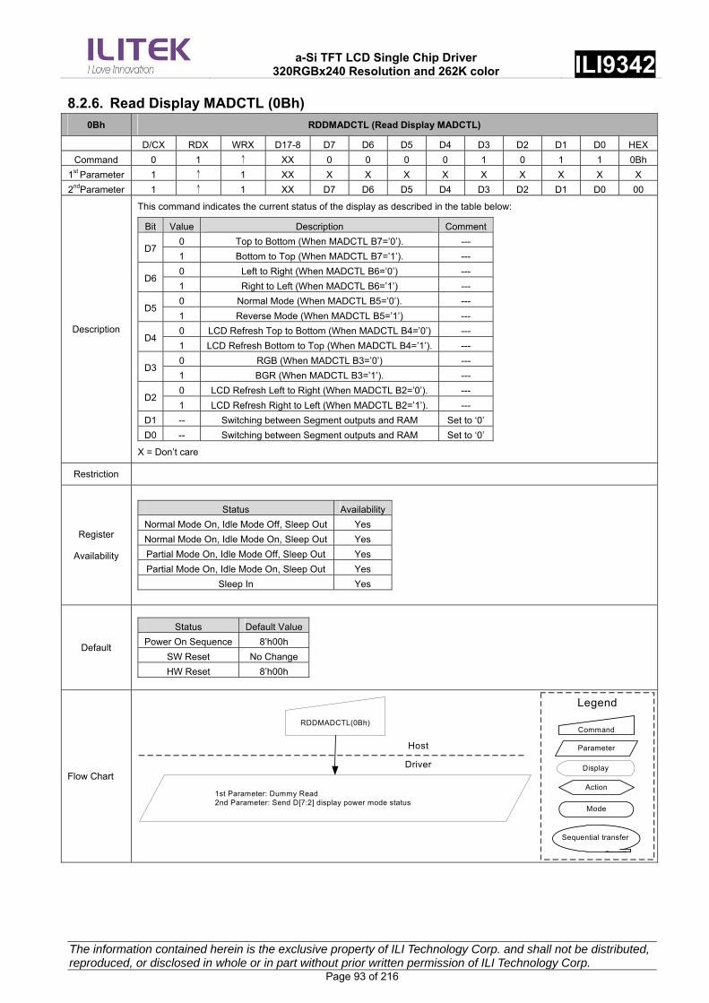
a-Si TFT LCD Single Chip Driver
320RGBx240 Resolution and 262K color ILI9342
The information contained herein is the exclusive property of ILI Technology Corp. and shall not be distributed, reproduced, or disclosed in whole or in part without prior written permission of ILI Technology Corp. Page 93 of 216
8.2.6. Read Display MADCTL (0Bh)
0Bh RDDMADCTL (Read Display MADCTL)
D/CX RDX WRX D17-8 D7 D6 D5 D4 D3 D2 D1 D0 HEX
Command 0 1 ↑ XX 0 0 0 0 1 0 1 1 0Bh
1st Parameter 1 ↑ 1 XX X X X X X X X X X
2ndParameter 1 ↑ 1 XX D7 D6 D5 D4 D3 D2 D1 D0 00
Description
This command indicates the current status of the display as described in the table below:
Bit Value Description Comment
0 Top to Bottom (When MADCTL B7=’0’). --- D7
1 Bottom to Top (When MADCTL B7=’1’). ---
0 Left to Right (When MADCTL B6=’0’) --- D6
1 Right to Left (When MADCTL B6=’1’) ---
0 Normal Mode (When MADCTL B5=’0’). --- D5
1 Reverse Mode (When MADCTL B5=’1’) ---
0 LCD Refresh Top to Bottom (When MADCTL B4=’0’) --- D4
1 LCD Refresh Bottom to Top (When MADCTL B4=’1’). ---
0 RGB (When MADCTL B3=’0’) --- D3
1 BGR (When MADCTL B3=’1’). ---
0 LCD Refresh Left to Right (When MADCTL B2=’0’). --- D2
1 LCD Refresh Right to Left (When MADCTL B2=’1’). ---
D1 -- Switching between Segment outputs and RAM Set to ‘0’
D0 -- Switching between Segment outputs and RAM Set to ‘0’
X = Don’t care
Restriction
Register
Availability
Status Availability
Normal Mode On, Idle Mode Off, Sleep Out Yes
Normal Mode On, Idle Mode On, Sleep Out Yes
Partial Mode On, Idle Mode Off, Sleep Out Yes
Partial Mode On, Idle Mode On, Sleep Out Yes
Sleep In Yes
Default
Status Default Value
Power On Sequence 8’h00h
SW Reset No Change
HW Reset 8’h00h
Flow Chart
Command
Parameter
Action
Mode
Legend
Sequential transfer
RDDMADCTL(0Bh)
1st Parameter: Dummy Read2nd Parameter: Send D[7:2] display power mode status
Host
Driver Display
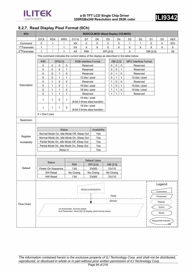
a-Si TFT LCD Single Chip Driver
320RGBx240 Resolution and 262K color ILI9342
The information contained herein is the exclusive property of ILI Technology Corp. and shall not be distributed, reproduced, or disclosed in whole or in part without prior written permission of ILI Technology Corp. Page 94 of 216
8.2.7. Read Display Pixel Format (0Ch)
0Ch RDDCOLMOD (Read Display COLMOD)
D/CX RDX WRX D17-8 D7 D6 D5 D4 D3 D2 D1 D0 HEX
Command 0 1 ↑ XX 0 0 0 0 1 1 0 0 0Ch
1st Parameter 1 ↑ 1 XX X X X X X X X X X
2ndParameter 1 ↑ 1 XX RIM DPI [2:0] 0 DBI [2:0] 06
Description
This command indicates the current status of the display as described in the table below:
RIM DPI[2:0] RGB Interface Format DBI [2:0] MPU Interface Format
0 0 0 0 Reserved 0 0 0 Reserved
0 0 0 1 Reserved 0 0 1 Reserved
0 0 1 0 Reserved 0 1 0 Reserved
0 0 1 1 12 bits / pixel 0 1 1 12 bits / pixel
0 1 0 0 Reserved 1 0 0 Reserved
0 1 0 1 16 bits / pixel 1 0 1 16 bits / pixel
0 1 1 0 18 bits / pixel 1 1 0 18 bits / pixel
0 1 1 1 Reserved 1 1 1 Reserved
1 1 0 1 16 bits / pixel
(6-bit 3 times data transfer)
1 1 1 0 18 bits / pixel
(6-bit 3 times data transfer)
X = Don’t care
Restriction
Register
Availability
Status Availability
Normal Mode On, Idle Mode Off, Sleep Out Yes
Normal Mode On, Idle Mode On, Sleep Out Yes
Partial Mode On, Idle Mode Off, Sleep Out Yes
Partial Mode On, Idle Mode On, Sleep Out Yes
Sleep In Yes
Default
Default Value Status
RIM DPI [2:0] DBI [2:0]
Power On Sequence 1’b0 3’b000 3’b110
SW Reset No Chang No Chang No Chang
HW Reset 1’b0 3’b000 3’b110
Flow Chart
Command
Parameter
Action
Mode
Legend
Sequential transfer
RDDCOLMOD(0Ch)
1st Parameter: Dummy Read2nd Parameter: Send D[7:2] display pixel format status
Host
Driver Display

a-Si TFT LCD Single Chip Driver
320RGBx240 Resolution and 262K color ILI9342
The information contained herein is the exclusive property of ILI Technology Corp. and shall not be distributed, reproduced, or disclosed in whole or in part without prior written permission of ILI Technology Corp. Page 95 of 216
8.2.8. Read Display Image Format (0Dh)
0Dh RDDIM (Read Display Image Mode)
D/CX RDX WRX D17-8 D7 D6 D5 D4 D3 D2 D1 D0 HEX
Command 0 1 ↑ XX 0 0 0 0 1 1 0 1 0Dh
1st Parameter 1 ↑ 1 XX X X X X X X X X X
2ndParameter 1 ↑ 1 XX 0 0 0 0 0 D [2:0] 00
Description
This command indicates the current status of the display as described in the table below:
D [2:0] Description 000 Gamma curve 1 (GC0 G2.2) 001 Gamma curve 2 (GC1 G1.8) 010 Gamma curve 3 (GC2 G2.5) 011 Gamma curve 4 (GC3 G1.0)
Other Not defined
X = Don’t care
Restriction
Register
Availability
Status Availability
Normal Mode On, Idle Mode Off, Sleep Out Yes
Normal Mode On, Idle Mode On, Sleep Out Yes
Partial Mode On, Idle Mode Off, Sleep Out Yes
Partial Mode On, Idle Mode On, Sleep Out Yes
Sleep In Yes
Default
Status Default Value
Power On Sequence 3’b000
SW Reset 3’b000
HW Reset 3’b000
Flow Chart
Command
Parameter
Action
Mode
Legend
Sequential transfer
RDDIM(0Dh)
1st Parameter: Dummy Read2nd Parameter: Send D[7:0] display image mode status
Host
Driver Display
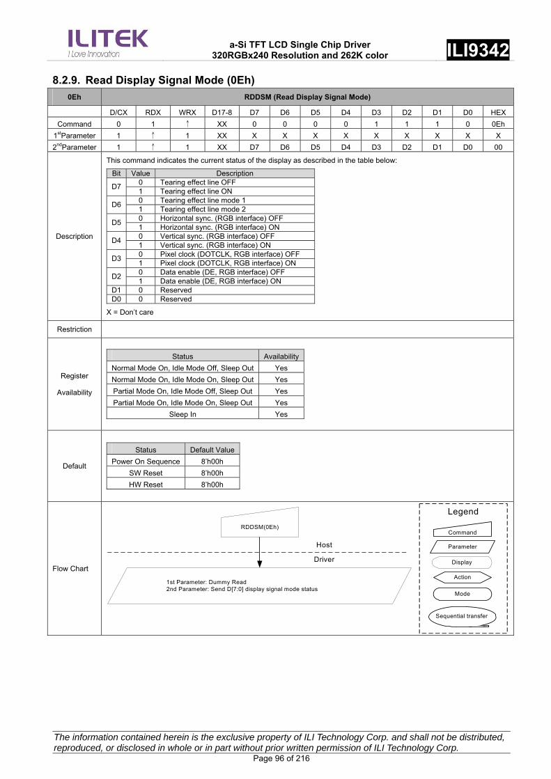
a-Si TFT LCD Single Chip Driver
320RGBx240 Resolution and 262K color ILI9342
The information contained herein is the exclusive property of ILI Technology Corp. and shall not be distributed, reproduced, or disclosed in whole or in part without prior written permission of ILI Technology Corp. Page 96 of 216
8.2.9. Read Display Signal Mode (0Eh)
0Eh RDDSM (Read Display Signal Mode)
D/CX RDX WRX D17-8 D7 D6 D5 D4 D3 D2 D1 D0 HEX
Command 0 1 ↑ XX 0 0 0 0 1 1 1 0 0Eh
1stParameter 1 ↑ 1 XX X X X X X X X X X
2ndParameter 1 ↑ 1 XX D7 D6 D5 D4 D3 D2 D1 D0 00
Description
This command indicates the current status of the display as described in the table below:
Bit Value Description 0 Tearing effect line OFF
D7 1 Tearing effect line ON 0 Tearing effect line mode 1
D6 1 Tearing effect line mode 2 0 Horizontal sync. (RGB interface) OFF
D5 1 Horizontal sync. (RGB interface) ON 0 Vertical sync. (RGB interface) OFF
D4 1 Vertical sync. (RGB interface) ON 0 Pixel clock (DOTCLK, RGB interface) OFF
D3 1 Pixel clock (DOTCLK, RGB interface) ON 0 Data enable (DE, RGB interface) OFF
D2 1 Data enable (DE, RGB interface) ON
D1 0 Reserved D0 0 Reserved
X = Don’t care
Restriction
Register
Availability
Status Availability
Normal Mode On, Idle Mode Off, Sleep Out Yes
Normal Mode On, Idle Mode On, Sleep Out Yes
Partial Mode On, Idle Mode Off, Sleep Out Yes
Partial Mode On, Idle Mode On, Sleep Out Yes
Sleep In Yes
Default
Status Default Value
Power On Sequence 8’h00h
SW Reset 8’h00h
HW Reset 8’h00h
Flow Chart
Command
Parameter
Action
Mode
Legend
Sequential transfer
RDDSM(0Eh)
1st Parameter: Dummy Read2nd Parameter: Send D[7:0] display signal mode status
Host
Driver Display

a-Si TFT LCD Single Chip Driver
320RGBx240 Resolution and 262K color ILI9342
The information contained herein is the exclusive property of ILI Technology Corp. and shall not be distributed, reproduced, or disclosed in whole or in part without prior written permission of ILI Technology Corp. Page 97 of 216
8.2.10. Read Display Self-Diagnostic Result (0Fh)
0Fh RDDSDR (Read Display Self-Diagnostic Result)
D/CX RDX WRX D17-8 D7 D6 D5 D4 D3 D2 D1 D0 HEX
Command 0 1 ↑ XX 0 0 0 0 1 1 1 1 0Fh
1stParameter 1 ↑ 1 XX X X X X X X X X X
2ndParameter 1 ↑ 1 XX D7 D6 0 0 0 0 0 0 00
Description
Bit Description Action
D7 Register Loading Detection Invert the D7 bit if register values loading work properly.
D6 Functionality Detection Invert the D6 bit if the display is functionality
D5 Not Used ‘0’
D4 Not Used ‘0’
D3 Not Used ‘0’
D2 Not Used ‘0’
D1 Not Used ‘0’
D0 Not Used ‘0’
Restriction
Register
Availability
Status Availability
Normal Mode On, Idle Mode Off, Sleep Out Yes
Normal Mode On, Idle Mode On, Sleep Out Yes
Partial Mode On, Idle Mode Off, Sleep Out Yes
Partial Mode On, Idle Mode On, Sleep Out Yes
Sleep In Yes
Default
Status Default Value
Power On Sequence 8’h00h
SW Reset 8’h00h
HW Reset 8’h00h
Flow Chart
Command
Parameter
Action
Mode
Legend
Sequential transfer
RDDSDR(0Fh)
1st Parameter: Dummy Read2nd Parameter: Send D[7:6] display self-diagnostic status
Host
Driver Display

a-Si TFT LCD Single Chip Driver
320RGBx240 Resolution and 262K color ILI9342
The information contained herein is the exclusive property of ILI Technology Corp. and shall not be distributed, reproduced, or disclosed in whole or in part without prior written permission of ILI Technology Corp. Page 98 of 216
8.2.11. Enter Sleep Mode (10h)
10h SPLIN (Enter Sleep Mode)
D/CX RDX WRX D17-8 D7 D6 D5 D4 D3 D2 D1 D0 HEX
Command 0 1 ↑ XX 0 0 0 1 0 0 0 0 10h
Parameter No Parameter
Description
This command causes the LCD module to enter the minimum power consumption mode. In this mode e.g. the DC/DC
converter is stopped, Internal oscillator is stopped, and panel scanning is stopped.
Out Blank STOP
MPU interface and memory are still working and the memory keeps its contents.
X = Don’t care
Restriction
This command has no effect when module is already in sleep in mode. Sleep In Mode can only be left by the Sleep Out
Command (11h). It will be necessary to wait 5msec before sending next to command, this is to allow time for the supply
voltages and clock circuits to stabilize. It will be necessary to wait 120msec after sending Sleep Out command (when in Sleep
In Mode) before Sleep In command can be sent.
Register
Availability
Status Availability
Normal Mode On, Idle Mode Off, Sleep Out Yes
Normal Mode On, Idle Mode On, Sleep Out Yes
Partial Mode On, Idle Mode Off, Sleep Out Yes
Partial Mode On, Idle Mode On, Sleep Out Yes
Sleep In Yes
Default
Status Default Value
Power On Sequence Sleep IN Mode
SW Reset Sleep IN Mode
HW Reset Sleep IN Mode
Flow Chart
It takes 120msec to get into Sleep In mode after SLPIN command issued.
Command
Parameter
Action
Mode
Legend
Sequential transfer
SPLIN (10h)
Display whole blank screen (Automatic No effect to DISP
ON/OFF commands)
Drain charge from LCD
panel
Stop DC/DC Converter
Stop Internal Oscillator
Sleep In Mode
Display

a-Si TFT LCD Single Chip Driver
320RGBx240 Resolution and 262K color ILI9342
The information contained herein is the exclusive property of ILI Technology Corp. and shall not be distributed, reproduced, or disclosed in whole or in part without prior written permission of ILI Technology Corp. Page 99 of 216
8.2.12. Sleep Out (11h)
11h SLPOUT (Sleep Out)
D/CX RDX WRX D17-8 D7 D6 D5 D4 D3 D2 D1 D0 HEX
Command 0 1 ↑ XX 0 0 0 1 0 0 0 1 11h
Parameter No Parameter
Description
This command turns off sleep mode.
In this mode e.g. the DC/DC converter is enabled, Internal oscillator is started, and panel scanning is started.
Internal Oscillator
DDVDH
VGL
VGH
IOVCC
VCI
1.65V ~ 3.6V
2.4V ~ 3.6V
Start
VCI
0V
VCI
X = Don’t care
Restriction
This command has no effect when module is already in sleep out mode. Sleep Out Mode can only be left by the Sleep In
Command (10h). It will be necessary to wait 5msec before sending next command, this is to allow time for the clock circuits
stabilize. The display module loads all display supplier’s factory default values to the registers during this 120msec and there
cannot be any abnormal visual effect on the display image if factory default and register values are same when this load is
done and when the display module is already Sleep Out –mode. The display module is doing self-diagnostic functions during
this 5msec. It will be necessary to wait 120msec after sending Sleep In command (when in Sleep Out mode) before Sleep Out
command can be sent.
Register
Availability
Status Availability
Normal Mode On, Idle Mode Off, Sleep Out Yes
Normal Mode On, Idle Mode On, Sleep Out Yes
Partial Mode On, Idle Mode Off, Sleep Out Yes
Partial Mode On, Idle Mode On, Sleep Out Yes
Sleep In Yes
Default
Status Default Value
Power On Sequence Sleep IN Mode
SW Reset Sleep IN Mode
HW Reset Sleep IN Mode
Flow Chart It takes 120msec to become Sleep Out mode after SLPOUT command issued.

a-Si TFT LCD Single Chip Driver
320RGBx240 Resolution and 262K color ILI9342
The information contained herein is the exclusive property of ILI Technology Corp. and shall not be distributed, reproduced, or disclosed in whole or in part without prior written permission of ILI Technology Corp. Page 100 of 216
SPLOUT (11h) Display whole blank screen for 2 frames (Automatic No
effect to DISP ON/OFF Commands)
Start up DC-DC
Converter
Sleep Out Mode
Charge Offset voltage for LCD Panel
Start Internal Oscillator
Display Memory contents in accordance with the current
command table settings
Command
Parameter
Action
Mode
Legend
Sequential transfer
Display
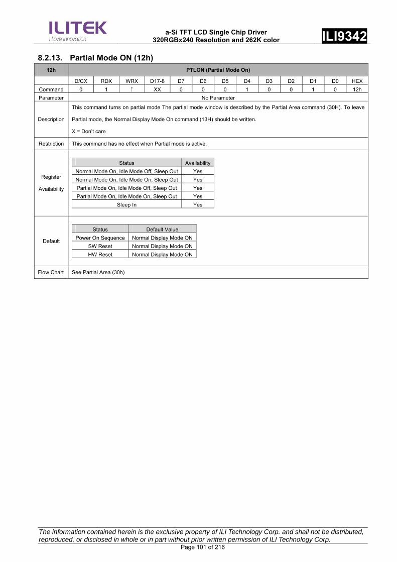
a-Si TFT LCD Single Chip Driver
320RGBx240 Resolution and 262K color ILI9342
The information contained herein is the exclusive property of ILI Technology Corp. and shall not be distributed, reproduced, or disclosed in whole or in part without prior written permission of ILI Technology Corp. Page 101 of 216
8.2.13. Partial Mode ON (12h)
12h PTLON (Partial Mode On)
D/CX RDX WRX D17-8 D7 D6 D5 D4 D3 D2 D1 D0 HEX
Command 0 1 ↑ XX 0 0 0 1 0 0 1 0 12h
Parameter No Parameter
Description
This command turns on partial mode The partial mode window is described by the Partial Area command (30H). To leave
Partial mode, the Normal Display Mode On command (13H) should be written.
X = Don’t care
Restriction This command has no effect when Partial mode is active.
Register
Availability
Status Availability
Normal Mode On, Idle Mode Off, Sleep Out Yes
Normal Mode On, Idle Mode On, Sleep Out Yes
Partial Mode On, Idle Mode Off, Sleep Out Yes
Partial Mode On, Idle Mode On, Sleep Out Yes
Sleep In Yes
Default
Status Default Value
Power On Sequence Normal Display Mode ON
SW Reset Normal Display Mode ON
HW Reset Normal Display Mode ON
Flow Chart See Partial Area (30h)

a-Si TFT LCD Single Chip Driver
320RGBx240 Resolution and 262K color ILI9342
The information contained herein is the exclusive property of ILI Technology Corp. and shall not be distributed, reproduced, or disclosed in whole or in part without prior written permission of ILI Technology Corp. Page 102 of 216
8.2.14. Normal Display Mode ON (13h)
13h NORON (Normal Display Mode On)
D/CX RDX WRX D17-8 D7 D6 D5 D4 D3 D2 D1 D0 HEX
Command 0 1 ↑ XX 0 0 0 1 0 0 1 1 13h
Parameter No Parameter
Description
This command returns the display to normal mode.
Normal display mode on means Partial mode off.
Exit from NORON by the Partial mode On command (12h)
X = Don’t care
Restriction This command has no effect when Normal Display mode is active.
Register
Availability
Status Availability
Normal Mode On, Idle Mode Off, Sleep Out Yes
Normal Mode On, Idle Mode On, Sleep Out Yes
Partial Mode On, Idle Mode Off, Sleep Out Yes
Partial Mode On, Idle Mode On, Sleep Out Yes
Sleep In Yes
Default
Status Default Value
Power On Sequence Normal Display Mode ON
SW Reset Normal Display Mode ON
HW Reset Normal Display Mode ON
Flow Chart See Partial Area (30h)

a-Si TFT LCD Single Chip Driver
320RGBx240 Resolution and 262K color ILI9342
The information contained herein is the exclusive property of ILI Technology Corp. and shall not be distributed, reproduced, or disclosed in whole or in part without prior written permission of ILI Technology Corp. Page 103 of 216
8.2.15. Display Inversion OFF (20h)
20h DINVOFF (Display Inversion OFF)
D/CX RDX WRX D17-8 D7 D6 D5 D4 D3 D2 D1 D0 HEX
Command 0 1 ↑ XX 0 0 1 0 0 0 0 0 20h
Parameter No Parameter
Description
This command is used to recover from display inversion mode.
This command makes no change of the content of frame memory.
This command doesn’t change any other status.
Memory Display Panel
X = Don’t care
Restriction This command has no effect when module already is inversion OFF mode.
Register
Availability
Status Availability
Normal Mode On, Idle Mode Off, Sleep Out Yes
Normal Mode On, Idle Mode On, Sleep Out Yes
Partial Mode On, Idle Mode Off, Sleep Out Yes
Partial Mode On, Idle Mode On, Sleep Out Yes
Sleep In Yes
Default
Status Default Value
Power On Sequence Display Inversion OFF
SW Reset Display Inversion OFF
HW Reset Display Inversion OFF
Flow Chart
INVOFF(20h)
Display Inversion Off Mode
Display Inversion On Mode
Command
Parameter
Action
Mode
Legend
Sequential transfer
Display
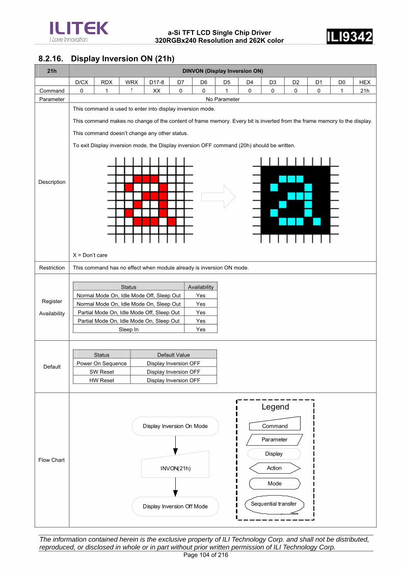
a-Si TFT LCD Single Chip Driver
320RGBx240 Resolution and 262K color ILI9342
The information contained herein is the exclusive property of ILI Technology Corp. and shall not be distributed, reproduced, or disclosed in whole or in part without prior written permission of ILI Technology Corp. Page 104 of 216
8.2.16. Display Inversion ON (21h)
21h DINVON (Display Inversion ON)
D/CX RDX WRX D17-8 D7 D6 D5 D4 D3 D2 D1 D0 HEX
Command 0 1 ↑ XX 0 0 1 0 0 0 0 1 21h
Parameter No Parameter
Description
This command is used to enter into display inversion mode.
This command makes no change of the content of frame memory. Every bit is inverted from the frame memory to the display.
This command doesn’t change any other status.
To exit Display inversion mode, the Display inversion OFF command (20h) should be written.
X = Don’t care
Restriction This command has no effect when module already is inversion ON mode.
Register
Availability
Status Availability
Normal Mode On, Idle Mode Off, Sleep Out Yes
Normal Mode On, Idle Mode On, Sleep Out Yes
Partial Mode On, Idle Mode Off, Sleep Out Yes
Partial Mode On, Idle Mode On, Sleep Out Yes
Sleep In Yes
Default
Status Default Value
Power On Sequence Display Inversion OFF
SW Reset Display Inversion OFF
HW Reset Display Inversion OFF
Flow Chart
INVON(21h)
Display Inversion Off Mode
Display Inversion On Mode Command
Parameter
Action
Mode
Legend
Sequential transfer
Display

a-Si TFT LCD Single Chip Driver
320RGBx240 Resolution and 262K color ILI9342
The information contained herein is the exclusive property of ILI Technology Corp. and shall not be distributed, reproduced, or disclosed in whole or in part without prior written permission of ILI Technology Corp. Page 105 of 216
8.2.17. Gamma Set (26h)
26h GAMSET (Gamma Set)
D/CX RDX WRX D17-8 D7 D6 D5 D4 D3 D2 D1 D0 HEX
Command 0 1 ↑ XX 0 0 1 0 0 1 1 0 26h
Parameter 1 1 ↑ XX GC [7:0] 01
Description
This command is used to select the desired Gamma curve for the current display. A maximum of 4 fixed gamma curves can
be selected. The curve is selected by setting the appropriate bit in the parameter as described in the Table:
GC [7:0] Curve Selected
01h Gamma curve 1 (G2.2)
02h Gamma curve 2 (G1.8)
04h Gamma curve 3 (G2.5)
08h Gamma curve 4 (G1.0)
Note: All other values are undefined.
X = Don’t care
Restriction Values of GC [7:0] not shown in table above are invalid and will not change the current selected Gamma curve until valid
value is received.
Register
Availability
Status Availability
Normal Mode On, Idle Mode Off, Sleep Out Yes
Normal Mode On, Idle Mode On, Sleep Out Yes
Partial Mode On, Idle Mode Off, Sleep Out Yes
Partial Mode On, Idle Mode On, Sleep Out Yes
Sleep In Yes
Default
Status Default Value
Power On Sequence 8’h01h
SW Reset 8’h01h
HW Reset 8’h01h
Flow Chart
GAMSET (26h)
1st Parameter: GC[7:0]
New Gamma Curve Loaded
Command
Parameter
Action
Mode
Legend
Sequential transfer
Display

a-Si TFT LCD Single Chip Driver
320RGBx240 Resolution and 262K color ILI9342
The information contained herein is the exclusive property of ILI Technology Corp. and shall not be distributed, reproduced, or disclosed in whole or in part without prior written permission of ILI Technology Corp. Page 106 of 216
8.2.18. Display OFF (28h)
28h DISPOFF (Display OFF)
D/CX RDX WRX D17-8 D7 D6 D5 D4 D3 D2 D1 D0 HEX
Command 0 1 ↑ XX 0 0 1 0 1 0 0 0 28h
Parameter No Parameter
Description
This command is used to enter into DISPLAY OFF mode. In this mode, the output from Frame Memory is disabled and blank
page inserted.
This command makes no change of contents of frame memory.
This command does not change any other status.
There will be no abnormal visible effect on the display.
Memory Display Panel
X = Don’t care.
Restriction This command has no effect when module is already in display off mode.
Register
Availability
Status Availability
Normal Mode On, Idle Mode Off, Sleep Out Yes
Normal Mode On, Idle Mode On, Sleep Out Yes
Partial Mode On, Idle Mode Off, Sleep Out Yes
Partial Mode On, Idle Mode On, Sleep Out Yes
Sleep In Yes
Default
Status Default Value
Power On Sequence Display OFF
SW Reset Display OFF
HW Reset Display OFF
Flow Chart
Display On Mode
DISPOFF(28h)
Display Off Mode
Command
Parameter
Action
Mode
Legend
Sequential transfer
Display

a-Si TFT LCD Single Chip Driver
320RGBx240 Resolution and 262K color ILI9342
The information contained herein is the exclusive property of ILI Technology Corp. and shall not be distributed, reproduced, or disclosed in whole or in part without prior written permission of ILI Technology Corp. Page 107 of 216
8.2.19. Display ON (29h)
29h DISPON (Display ON)
D/CX RDX WRX D17-8 D7 D6 D5 D4 D3 D2 D1 D0 HEX
Command 0 1 ↑ XX 0 0 1 0 1 0 0 1 29h
Parameter No Parameter
Description
This command is used to recover from DISPLAY OFF mode. Output from the Frame Memory is enabled.
This command makes no change of contents of frame memory.
This command does not change any other status
Memory Display Panel
X = Don’t care.
Restriction This command has no effect when module is already in display on mode.
Register
Availability
Status Availability
Normal Mode On, Idle Mode Off, Sleep Out Yes
Normal Mode On, Idle Mode On, Sleep Out Yes
Partial Mode On, Idle Mode Off, Sleep Out Yes
Partial Mode On, Idle Mode On, Sleep Out Yes
Sleep In Yes
Default
Status Default Value
Power On Sequence Display OFF
SW Reset Display OFF
HW Reset Display OFF
Flow Chart
Display Off Mode
DISPON(29h)
Display On Mode
Command
Parameter
Action
Mode
Legend
Sequential transfer
Display

a-Si TFT LCD Single Chip Driver
320RGBx240 Resolution and 262K color ILI9342
The information contained herein is the exclusive property of ILI Technology Corp. and shall not be distributed, reproduced, or disclosed in whole or in part without prior written permission of ILI Technology Corp. Page 108 of 216
8.2.20. Column Address Set (2Ah)
2Ah CASET (Column Address Set)
D/CX RDX WRX D17-8 D7 D6 D5 D4 D3 D2 D1 D0 HEX
Command 0 1 ↑ XX 0 0 1 0 1 0 1 0 2Ah
1st Parameter 1 1 ↑ XX SC15 SC14 SC13 SC12 SC11 SC10 SC9 SC8
2ndParameter 1 1 ↑ XX SC7 SC6 SC5 SC4 SC3 SC2 SC1 SC0 Note1
3rd Parameter 1 1 ↑ XX EC15 EC14 EC13 EC12 EC11 EC10 EC9 EC8
4th Parameter 1 1 ↑ XX EC7 EC6 EC5 EC4 EC3 EC2 EC1 EC0 Note1
Description
This command is used to define area of frame memory where MPU can access. This command makes no change on the
other driver status. The values of SC [15:0] and EC [15:0] are referred when RAMWR command comes. Each value
represents one column line in the Frame Memory.
SC[15:0] EC[15:0]
X = Don’t care
Restriction
SC [15:0] always must be equal to or less than EC [15:0].
Note 1: When SC [15:0] or EC [15:0] is greater than 013Fh (When MADCTL’s B5 = 0) or 00EFh
(When MADCTL’s B5 = 1), data of out of range will be ignored
Register
Availability
Status Availability
Normal Mode On, Idle Mode Off, Sleep Out Yes
Normal Mode On, Idle Mode On, Sleep Out Yes
Partial Mode On, Idle Mode Off, Sleep Out Yes
Partial Mode On, Idle Mode On, Sleep Out Yes
Sleep In Yes
Default
Status Default Value
Power On Sequence SC [15:0]=0000h EC [15:0]=013Fh
SW Reset SC [15:0]=0000hIf MADCTL’s B5 = 0: EC [15:0]=013Fh
If MADCTL’s B5 = 1: EC [15:0]=00EFh
HW Reset SC [15:0]=0000h EC [15:0]=013Fh

a-Si TFT LCD Single Chip Driver
320RGBx240 Resolution and 262K color ILI9342
The information contained herein is the exclusive property of ILI Technology Corp. and shall not be distributed, reproduced, or disclosed in whole or in part without prior written permission of ILI Technology Corp. Page 109 of 216
Flow Chart
CASET (2Ah)
1st Parameter: SC[15:8]2nd Parameter: SC[7:0]3rd Parameter: EC[15:8]4th Parmeter EC[7:0]
PASET (2Bh)
1st Parameter: SP[15:8]2nd Parameter: SP[7:0]3rd Parameter: EP[15:8]4th Parameter: EP[7:0]
RAMWR(2Ch)
Image DataD1[17:0],D2[17:0]..Dn[17:0]
Any Commend
If Needed
If Needed
Command
Parameter
Action
Mode
Legend
Sequential transfer
Display

a-Si TFT LCD Single Chip Driver
320RGBx240 Resolution and 262K color ILI9342
The information contained herein is the exclusive property of ILI Technology Corp. and shall not be distributed, reproduced, or disclosed in whole or in part without prior written permission of ILI Technology Corp. Page 110 of 216
8.2.21. Page Address Set (2Bh)
2Bh PASET (Page Address Set)
D/CX RDX WRX D17-8 D7 D6 D5 D4 D3 D2 D1 D0 HEX
Command 0 1 ↑ XX 0 0 1 0 1 0 1 1 2Bh
1st Parameter 1 1 ↑ XX SP15 SP14 SP13 SP12 SP11 SP10 SP9 SP8
2ndParameter 1 1 ↑ XX SP7 SP6 SP5 SP4 SP3 SP2 SP1 SP0 Note1
3rdParameter 1 1 ↑ XX EP15 EP14 EP13 EP12 EP11 EP10 EP9 EP8
4th Parameter 1 1 ↑ XX EP7 EP6 EP5 EP4 EP3 EP2 EP1 EP0 Note1
Description
This command is used to define area of frame memory where MPU can access. This command makes no change on the
other driver status. The values of SP [15:0] and EP [15:0] are referred when RAMWR command comes. Each value
represents one Page line in the Frame Memory.
SP[15:0]
EP[15:0]
X = Don’t care
Restriction
SP [15:0] always must be equal to or less than EP [15:0]
Note 1: When SP [15:0] or EP [15:0] is greater than 00EFh (When MADCTL’s B5 = 0) or 013Fh (When MADCTL’s B5 = 1),
data of out of range will be ignored.
Register
Availability
Status Availability
Normal Mode On, Idle Mode Off, Sleep Out Yes
Normal Mode On, Idle Mode On, Sleep Out Yes
Partial Mode On, Idle Mode Off, Sleep Out Yes
Partial Mode On, Idle Mode On, Sleep Out Yes
Sleep In Yes
Default
Status Default Value
Power On Sequence SP [15:0]=0000h EP [15:0]=00EFh
SW Reset SP [15:0]=0000hIf MADCTL’s B5 = 0: EP [15:0]=00EFh
If MADCTL’s B5 = 1: EP [15:0]=013Fh
HW Reset SP [15:0]=0000h EP [15:0]=00EFh

a-Si TFT LCD Single Chip Driver
320RGBx240 Resolution and 262K color ILI9342
The information contained herein is the exclusive property of ILI Technology Corp. and shall not be distributed, reproduced, or disclosed in whole or in part without prior written permission of ILI Technology Corp. Page 111 of 216
Flow Chart
CASET (2Ah)
1st Parameter: SC[15:8]2nd Parameter: SC[7:0]3rd Parameter: EC[15:8]4th Parmeter EC[7:0]
PASET (2Bh)
1st Parameter: SP[15:8]2nd Parameter: SP[7:0]3rd Parameter: EP[15:8]4th Parameter: EP[7:0]
RAMWR(2Ch)
Image DataD1[17:0],D2[17:0]..Dn[17:0]
Any Commend
If Needed
If Needed
Command
Parameter
Action
Mode
Legend
Sequential transfer
Display

a-Si TFT LCD Single Chip Driver
320RGBx240 Resolution and 262K color ILI9342
The information contained herein is the exclusive property of ILI Technology Corp. and shall not be distributed, reproduced, or disclosed in whole or in part without prior written permission of ILI Technology Corp. Page 112 of 216
8.2.22. Memory Write (2Ch)
2Ch RAMWR (Memory Write)
D/CX RDX WRX D17-8 D7 D6 D5 D4 D3 D2 D1 D0 HEX
Command 0 1 ↑ XX 0 0 1 0 1 1 0 0 2Ch
1st Parameter 1 1 ↑ D1 [17:0] XX
: 1 1 ↑ Dx [17:0] XX
Nth Parameter 1 1 ↑ Dn [17:0] XX
Description
This command is used to transfer data from MPU to frame memory. This command makes no change to the other driver
status. When this command is accepted, the column register and the page register are reset to the Start Column/Start
Page positions. The Start Column/Start Page positions are different in accordance with MADCTL setting.) Then D [17:0] is
stored in frame memory and the column register and the page register incremented. Sending any other command can stop
frame Write. X = Don’t care.
Restriction In all color modes, there is no restriction on length of parameters.
Register
Availability
Status Availability
Normal Mode On, Idle Mode Off, Sleep Out Yes
Normal Mode On, Idle Mode On, Sleep Out Yes
Partial Mode On, Idle Mode Off, Sleep Out Yes
Partial Mode On, Idle Mode On, Sleep Out Yes
Sleep In Yes
Default
Status Default Value
Power On Sequence Contents of memory is set randomly
SW Reset Contents of memory is not cleared
HW Reset Contents of memory is not cleared
Flow Chart
CASET (2Ah)
1st Parameter: SC[15:8]2nd Parameter: SC[7:0]3rd Parameter: EC[15:8]4th Parmeter EC[7:0]
PASET (2Bh)
1st Parameter: SP[15:8]2nd Parameter: SP[7:0]3rd Parameter: EP[15:8]4th Parameter: EP[7:0]
RAMWR(2Ch)
Image DataD1[17:0],D2[17:0]..Dn[17:0]
Any Commend
If Needed
If Needed
Command
Parameter
Action
Mode
Legend
Sequential transfer
Display
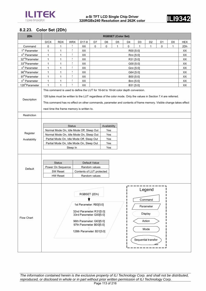
a-Si TFT LCD Single Chip Driver
320RGBx240 Resolution and 262K color ILI9342
The information contained herein is the exclusive property of ILI Technology Corp. and shall not be distributed, reproduced, or disclosed in whole or in part without prior written permission of ILI Technology Corp. Page 113 of 216
8.2.23. Color Set (2Dh)
2Dh RGBSET (Color Set)
D/CX RDX WRX D17-8 D7 D6 D5 D4 D3 D2 D1 D0 HEX
Command 0 1 ↑ XX 0 0 1 0 1 1 0 1 2Dh
1st Parameter 1 1 ↑ XX R00 [5:0] XX
nth Parameter 1 1 ↑ XX Rnn [5:0] XX
32ndParameter 1 1 ↑ XX R31 [5:0] XX
33rdParameter 1 1 ↑ XX G00 [5:0] XX
nth Parameter 1 1 ↑ XX Gnn [5:0] XX
96thParameter 1 1 ↑ XX G64 [5:0] XX
97thParameter 1 1 ↑ XX B00 [5:0] XX
nth Parameter 1 1 ↑ XX Bnn [5:0] XX
128thParameter 1 1 ↑ XX B31 [5:0] XX
Description
This command is used to define the LUT for 16-bit to 18-bit color depth conversion.
128 bytes must be written to the LUT regardless of the color mode. Only the values in Section 7.4 are referred.
This command has no effect on other commands, parameter and contents of frame memory. Visible change takes effect
next time the frame memory is written to.
Restriction
Register
Availability
Status Availability
Normal Mode On, Idle Mode Off, Sleep Out Yes
Normal Mode On, Idle Mode On, Sleep Out Yes
Partial Mode On, Idle Mode Off, Sleep Out Yes
Partial Mode On, Idle Mode On, Sleep Out Yes
Sleep In Yes
Default
Status Default Value
Power On Sequence Random values
SW Reset Contents of LUT protected
HW Reset Random values
Flow Chart
RGBSET (2Dh)
1st Parameter: R00[5:0]:
32nd Parameter: R31[5:0]33rd Parameter: G00[5:0]
:96th Parameter: G63[5:0]97th Parameter: B00[5:0]
:128th Parameter: B31[5:0]
Command
Parameter
Action
Mode
Legend
Sequential transfer
Display

a-Si TFT LCD Single Chip Driver
320RGBx240 Resolution and 262K color ILI9342
The information contained herein is the exclusive property of ILI Technology Corp. and shall not be distributed, reproduced, or disclosed in whole or in part without prior written permission of ILI Technology Corp. Page 114 of 216
8.2.24. Memory Read (2Eh)
2Eh RAMRD (Memory Read)
D/CX RDX WRX D17-8 D7 D6 D5 D4 D3 D2 D1 D0 HEX
Command 0 1 ↑ XX 0 0 1 0 1 1 1 0 2Eh
1stParameter 1 1 ↑ XX X X X X X X X X X
2ndParameter 1 1 ↑ D1 [17:0] XX
: 1 1 ↑ Dx [17:0] XX
(N+1)th
Parameter 1 1 ↑ Dn [17:0] XX
Description
This command transfers image data from ILI9342’s frame memory to the host processor starting at the pixel location
specified by preceding set_column_address and set_page_address commands.
If Memory Access control B5 = 0:
The column and page registers are reset to the Start Column (SC) and Start Page (SP), respectively. Pixels are read from
frame memory at (SC, SP). The column register is then incremented and pixels read from the frame memory until the
column register equals the End Column (EC) value. The column register is then reset to SC and the page register is
incremented. Pixels are read from the frame memory until the page register equals the End Page (EP) value or the host
processor sends another command.
If Memory Access Control B5 = 1:
The column and page registers are reset to the Start Column (SC) and Start Page (SP), respectively. Pixels are read from
frame memory at (SC, SP). The page register is then incremented and pixels read from the frame memory until the page
register equals the End Page (EP) value. The page register is then reset to SP and the column register is incremented.
Pixels are read from the frame memory until the column register equals the End Column (EC) value or the host processor
sends another command.
Restriction There is no restriction on length of parameters.
Register
Availability
Status Availability
Normal Mode On, Idle Mode Off, Sleep Out Yes
Normal Mode On, Idle Mode On, Sleep Out Yes
Partial Mode On, Idle Mode Off, Sleep Out Yes
Partial Mode On, Idle Mode On, Sleep Out Yes
Sleep In Yes
Default
Status Default Value
Power On Sequence Contents of memory is set randomly
SW Reset Contents of memory is set randomly
HW Reset Contents of memory is set randomly

a-Si TFT LCD Single Chip Driver
320RGBx240 Resolution and 262K color ILI9342
The information contained herein is the exclusive property of ILI Technology Corp. and shall not be distributed, reproduced, or disclosed in whole or in part without prior written permission of ILI Technology Corp. Page 115 of 216
Flow Chart
RAMRD (2Eh)
Dummy Read
Image DataD1[17:0],D2[17:0]..Dn[17:0]
Any Command
Command
Parameter
Action
Mode
Legend
Sequential transfer
Display

a-Si TFT LCD Single Chip Driver
320RGBx240 Resolution and 262K color ILI9342
The information contained herein is the exclusive property of ILI Technology Corp. and shall not be distributed, reproduced, or disclosed in whole or in part without prior written permission of ILI Technology Corp. Page 116 of 216
8.2.25. Partial Area (30h)
30h PLTAR (Partial Area)
D/CX RDX WRX D17-8 D7 D6 D5 D4 D3 D2 D1 D0 HEX
Command 0 1 ↑ XX 0 0 1 1 0 0 0 0 30h
1st Parameter 1 1 ↑ XX SR15 SR14 SR13 SR12 SR11 SR10 SR9 SR8 00
2ndParameter 1 1 ↑ XX SR7 SR6 SR5 SR4 SR3 SR2 SR1 SR0 00
3rdParameter 1 1 ↑ XX ER15 ER14 ER13 ER12 ER11 ER10 ER9 ER8 00
4th Parameter 1 1 ↑ XX ER7 ER6 ER5 ER4 ER3 ER2 ER1 ER0 EF
Description
This command defines the partial mode’s display area. There are 2 parameters associated with this command, the first
defines the Start Row (SR) and the second the End Row (ER), as illustrated in the figures below. SR and ER refer to the
Frame Memory Line Pointer.
If End Row>Start Row when MADCTL B4=0:-
SR[15:0]
ER[15:0]
Partial Area
End Row
Start Row
If End Row>Start Row when MADCTL B4=1:-
SR[15:0]
ER[15:0]
Partial Area
End Row
Start Row
If End Row<Start Row when MADCTL B4=0:-
SR[15:0]
ER[15:0]
Partial AreaEnd Row
Start Row
Partial Area
If End Row = Start Row then the Partial Area will be one row deep.
X = Don’t care.
Restriction SR [15…0] and ER [15…0] cannot be 0000h nor exceed 00EFh.

a-Si TFT LCD Single Chip Driver
320RGBx240 Resolution and 262K color ILI9342
The information contained herein is the exclusive property of ILI Technology Corp. and shall not be distributed, reproduced, or disclosed in whole or in part without prior written permission of ILI Technology Corp. Page 117 of 216
Register
Availability
Status Availability
Normal Mode On, Idle Mode Off, Sleep Out Yes
Normal Mode On, Idle Mode On, Sleep Out Yes
Partial Mode On, Idle Mode Off, Sleep Out Yes
Partial Mode On, Idle Mode On, Sleep Out Yes
Sleep In Yes
Default
Default Value Status
SR [15:0] ER [15:0]
Power On Sequence 16’h0000h 16’h00EFh
SW Reset 16’h 0000h 16’h 00EFh
HW Reset 16’h 0000h 16’h 00EFh
Flow Chart
1. To Enter Partial Mode
PLTAR(30h)
PTLON(12h)
1st Parameter: SR[15:8]2nd Parameter: SR[7:0]
3rd Parameter: ER[15:8]4th Parameter: ER[7:0]
Partial Mode
Command
Parameter
Action
Mode
Legend
Sequential transfer
Display
2. To Leave Partial Mode
DISPOFF(28h)
Image DataD1[17:0],D2[17:0]..Dn[17:0]
RAMRW(2Ch)
Partial Mode
NORON(13h)
Partial Mode OFF
DISPON(29h)
Command
Parameter
Action
Mode
Legend
Sequential transfer
Display
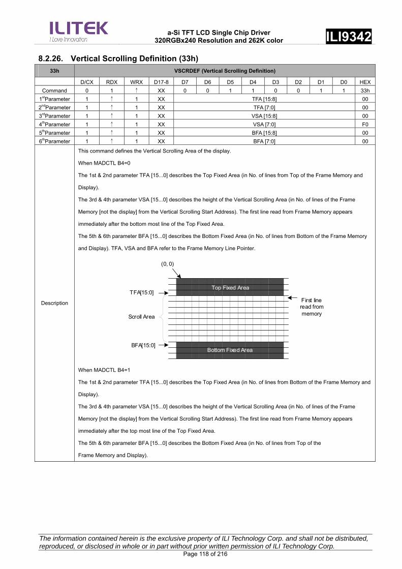
a-Si TFT LCD Single Chip Driver
320RGBx240 Resolution and 262K color ILI9342
The information contained herein is the exclusive property of ILI Technology Corp. and shall not be distributed, reproduced, or disclosed in whole or in part without prior written permission of ILI Technology Corp. Page 118 of 216
8.2.26. Vertical Scrolling Definition (33h)
33h VSCRDEF (Vertical Scrolling Definition)
D/CX RDX WRX D17-8 D7 D6 D5 D4 D3 D2 D1 D0 HEX
Command 0 1 ↑ XX 0 0 1 1 0 0 1 1 33h
1stParameter 1 ↑ 1 XX TFA [15:8] 00
2ndParameter 1 ↑ 1 XX TFA [7:0] 00
3rdParameter 1 ↑ 1 XX VSA [15:8] 00
4thParameter 1 ↑ 1 XX VSA [7:0] F0
5thParameter 1 ↑ 1 XX BFA [15:8] 00
6thParameter 1 ↑ 1 XX BFA [7:0] 00
Description
This command defines the Vertical Scrolling Area of the display.
When MADCTL B4=0
The 1st & 2nd parameter TFA [15...0] describes the Top Fixed Area (in No. of lines from Top of the Frame Memory and
Display).
The 3rd & 4th parameter VSA [15...0] describes the height of the Vertical Scrolling Area (in No. of lines of the Frame
Memory [not the display] from the Vertical Scrolling Start Address). The first line read from Frame Memory appears
immediately after the bottom most line of the Top Fixed Area.
The 5th & 6th parameter BFA [15...0] describes the Bottom Fixed Area (in No. of lines from Bottom of the Frame Memory
and Display). TFA, VSA and BFA refer to the Frame Memory Line Pointer.
Top Fixed Area
Bottom Fixed Area
TFA[15:0]
BFA[15:0]
(0, 0)
First line read from memoryScroll Area
When MADCTL B4=1
The 1st & 2nd parameter TFA [15...0] describes the Top Fixed Area (in No. of lines from Bottom of the Frame Memory and
Display).
The 3rd & 4th parameter VSA [15...0] describes the height of the Vertical Scrolling Area (in No. of lines of the Frame
Memory [not the display] from the Vertical Scrolling Start Address). The first line read from Frame Memory appears
immediately after the top most line of the Top Fixed Area.
The 5th & 6th parameter BFA [15...0] describes the Bottom Fixed Area (in No. of lines from Top of the
Frame Memory and Display).

a-Si TFT LCD Single Chip Driver
320RGBx240 Resolution and 262K color ILI9342
The information contained herein is the exclusive property of ILI Technology Corp. and shall not be distributed, reproduced, or disclosed in whole or in part without prior written permission of ILI Technology Corp. Page 119 of 216
Bottom Fixed Area
Top Fixed AreaTFA[15:0]
BFA[15:0]
(0, 0)
First line read from memory
Scroll Area
X = Don’t care
Restriction
Register
Availability
Status Availability
Normal Mode On, Idle Mode Off, Sleep Out Yes
Normal Mode On, Idle Mode On, Sleep Out Yes
Partial Mode On, Idle Mode Off, Sleep Out Yes
Partial Mode On, Idle Mode On, Sleep Out Yes
Sleep In Yes
Default
Default Value Status
TFA [15:0] VSA [15:0] BFA [15:0]
Power On Sequence 16’h0000h 16’h00EFh 16’h0000h
SW Reset 16’h0000h 16’h00EFh 16’h0000h
HW Reset 16’h0000h 16’h00EFh 16’h0000h
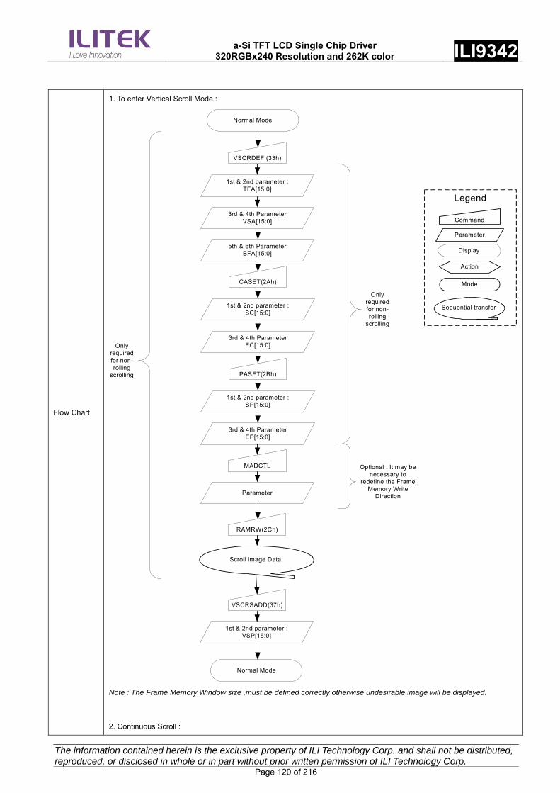
a-Si TFT LCD Single Chip Driver
320RGBx240 Resolution and 262K color ILI9342
The information contained herein is the exclusive property of ILI Technology Corp. and shall not be distributed, reproduced, or disclosed in whole or in part without prior written permission of ILI Technology Corp. Page 120 of 216
Flow Chart
1. To enter Vertical Scroll Mode :
Normal Mode
CASET(2Ah)
1st & 2nd parameter : SC[15:0]
3rd & 4th Parameter EC[15:0]
PASET(2Bh)
1st & 2nd parameter : SP[15:0]
3rd & 4th Parameter EP[15:0]
RAMRW(2Ch)
Scroll Image Data
VSCRSADD(37h)
1st & 2nd parameter : VSP[15:0]
Only required for non-rolling
scrolling
Command
Parameter
Action
Mode
Legend
Sequential transfer
Display
Normal Mode
Only required for non-rolling
scrolling
VSCRDEF (33h)
1st & 2nd parameter : TFA[15:0]
3rd & 4th Parameter VSA[15:0]
5th & 6th Parameter BFA[15:0]
MADCTL
Parameter
Optional : It may be necessary to
redefine the Frame Memory Write
Direction
Note : The Frame Memory Window size ,must be defined correctly otherwise undesirable image will be displayed.
2. Continuous Scroll :
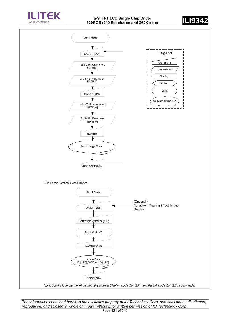
a-Si TFT LCD Single Chip Driver
320RGBx240 Resolution and 262K color ILI9342
The information contained herein is the exclusive property of ILI Technology Corp. and shall not be distributed, reproduced, or disclosed in whole or in part without prior written permission of ILI Technology Corp. Page 121 of 216
Scroll Mode
PASET (2Bh)
1st & 2nd parameter : SP[15:0]
3rd & 4th Parameter EP[15:0]
CASET (2Ah)
1st & 2nd parameter : SC[15:0]
3rd & 4th Parameter EC[15:0]
RAMRW
Scroll Image Data
VSCRSADD(37h)
Command
Parameter
Action
Mode
Legend
Sequential transfer
Display
3.To Leave Vertical Scroll Mode:
Scroll Mode
DISOFF(28h)
MORON(12h)/PTLON(12h)
Image Data D1[17:0],D2[17:0]...Dn[17:0]
DISON(29h)
Scroll Mode Off
RAMRW(2Ch)
(Optional )To prevent Tearing Effect Image Display
Note: Scroll Mode can be left by both the Normal Display Mode ON (13h) and Partial Mode ON (12h) commands.

a-Si TFT LCD Single Chip Driver
320RGBx240 Resolution and 262K color ILI9342
The information contained herein is the exclusive property of ILI Technology Corp. and shall not be distributed, reproduced, or disclosed in whole or in part without prior written permission of ILI Technology Corp. Page 122 of 216
8.2.27. Tearing Effect Line OFF (34h)
34h TEOFF (Tearing Effect Line OFF)
D/CX RDX WRX D17-8 D7 D6 D5 D4 D3 D2 D1 D0 HEX
Command 0 1 ↑ XX 0 0 1 1 0 1 0 0 34h
Parameter No Parameter
Description This command is used to turn OFF (Active Low) the Tearing Effect output signal from the TE signal line.
X = Don’t care.
Restriction This command has no effect when Tearing Effect output is already OFF.
Register
Availability
Status Availability
Normal Mode On, Idle Mode Off, Sleep Out Yes
Normal Mode On, Idle Mode On, Sleep Out Yes
Partial Mode On, Idle Mode Off, Sleep Out Yes
Partial Mode On, Idle Mode On, Sleep Out Yes
Sleep In Yes
Default
Status Default Value
Power On Sequence OFF
SW Reset OFF
HW Reset OFF
Flow Chart
TE Line Output ON
TEOFF(34h)
TE Line Output OFF
Command
Parameter
Action
Mode
Legend
Sequential transfer
Display
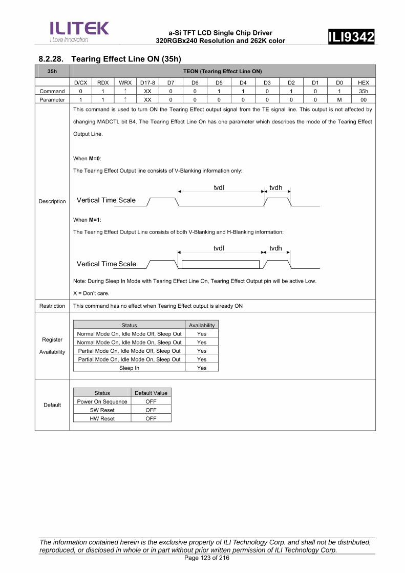
a-Si TFT LCD Single Chip Driver
320RGBx240 Resolution and 262K color ILI9342
The information contained herein is the exclusive property of ILI Technology Corp. and shall not be distributed, reproduced, or disclosed in whole or in part without prior written permission of ILI Technology Corp. Page 123 of 216
8.2.28. Tearing Effect Line ON (35h)
35h TEON (Tearing Effect Line ON)
D/CX RDX WRX D17-8 D7 D6 D5 D4 D3 D2 D1 D0 HEX
Command 0 1 ↑ XX 0 0 1 1 0 1 0 1 35h
Parameter 1 1 ↑ XX 0 0 0 0 0 0 0 M 00
Description
This command is used to turn ON the Tearing Effect output signal from the TE signal line. This output is not affected by
changing MADCTL bit B4. The Tearing Effect Line On has one parameter which describes the mode of the Tearing Effect
Output Line.
When M=0:
The Tearing Effect Output line consists of V-Blanking information only:
Vertical Time Scale
tvdl tvdh
When M=1:
The Tearing Effect Output Line consists of both V-Blanking and H-Blanking information:
Vertical Time Scale
tvdl tvdh
Note: During Sleep In Mode with Tearing Effect Line On, Tearing Effect Output pin will be active Low.
X = Don’t care.
Restriction This command has no effect when Tearing Effect output is already ON
Register
Availability
Status Availability
Normal Mode On, Idle Mode Off, Sleep Out Yes
Normal Mode On, Idle Mode On, Sleep Out Yes
Partial Mode On, Idle Mode Off, Sleep Out Yes
Partial Mode On, Idle Mode On, Sleep Out Yes
Sleep In Yes
Default
Status Default Value
Power On Sequence OFF
SW Reset OFF
HW Reset OFF

a-Si TFT LCD Single Chip Driver
320RGBx240 Resolution and 262K color ILI9342
The information contained herein is the exclusive property of ILI Technology Corp. and shall not be distributed, reproduced, or disclosed in whole or in part without prior written permission of ILI Technology Corp. Page 124 of 216
Flow Chart
TE Line Output OFF
TEON(35h)
TE Line Output ON
1st Parameter: M bit
Command
Parameter
Action
Mode
Legend
Sequential transfer
Display
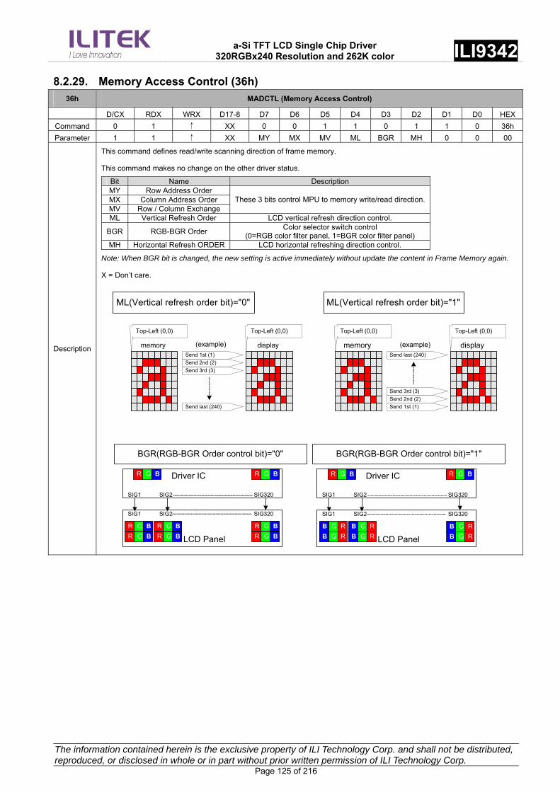
a-Si TFT LCD Single Chip Driver
320RGBx240 Resolution and 262K color ILI9342
The information contained herein is the exclusive property of ILI Technology Corp. and shall not be distributed, reproduced, or disclosed in whole or in part without prior written permission of ILI Technology Corp. Page 125 of 216
8.2.29. Memory Access Control (36h)
36h MADCTL (Memory Access Control)
D/CX RDX WRX D17-8 D7 D6 D5 D4 D3 D2 D1 D0 HEX
Command 0 1 ↑ XX 0 0 1 1 0 1 1 0 36h
Parameter 1 1 ↑ XX MY MX MV ML BGR MH 0 0 00
Description
This command defines read/write scanning direction of frame memory.
This command makes no change on the other driver status.
Bit Name Description MY Row Address Order MX Column Address Order MV Row / Column Exchange
These 3 bits control MPU to memory write/read direction.
ML Vertical Refresh Order LCD vertical refresh direction control.
BGR RGB-BGR Order Color selector switch control
(0=RGB color filter panel, 1=BGR color filter panel) MH Horizontal Refresh ORDER LCD horizontal refreshing direction control.
Note: When BGR bit is changed, the new setting is active immediately without update the content in Frame Memory again.
X = Don’t care.
Top-Left (0,0)Top-Left (0,0)
memory display
Send last (240)
Send 3rd (3)
Send 2nd (2)
Send 1st (1)
Top-Left (0,0)Top-Left (0,0)
memory display
Send 1st (1)
Send 3rd (3)
Send 2nd (2)
Send last (240)
(example) (example)
ML(Vertical refresh order bit)="1"ML(Vertical refresh order bit)="0"
R RG B G BDriver IC
SIG1 SIG2 SIG320
R G B
LCD Panel
SIG1 SIG2 SIG320
R G B
R G B
R G B
R G B
R G B
R RG B G BDriver IC
SIG1 SIG2 SIG320
RG B
LCD Panel
SIG1 SIG2 SIG320
RGB
R GB
RGB
RB G
RGB
BGR(RGB-BGR Order control bit)="0" BGR(RGB-BGR Order control bit)="1"

a-Si TFT LCD Single Chip Driver
320RGBx240 Resolution and 262K color ILI9342
The information contained herein is the exclusive property of ILI Technology Corp. and shall not be distributed, reproduced, or disclosed in whole or in part without prior written permission of ILI Technology Corp. Page 126 of 216
display
Sen
d la
st (
320)
Sen
d 3r
d (3
)
Sen
d 2n
d (2
)
Sen
d 1s
t (1)
Top-Left (0,0)
memory
Top-Left (0,0)
display
Send last (320
)
Send
3rd (3)
Sen
d 2nd (2
)
Se
nd 1st (1)
Top-Left (0,0)
memory
Top-Left (0,0)
MH(Horizontal refresh order control bit)="1"MH(Horizontal refresh order control bit)="0"
Note: Top-Left (0,0) means a physical memory location.
Restriction
Register
Availability
Status Availability
Normal Mode On, Idle Mode Off, Sleep Out Yes
Normal Mode On, Idle Mode On, Sleep Out Yes
Partial Mode On, Idle Mode Off, Sleep Out Yes
Partial Mode On, Idle Mode On, Sleep Out Yes
Sleep In Yes
Default
Status Default Value
Power On Sequence 8’h00h
SW Reset No change
HW Reset 8’h00h
Flow Chart
MADCTR(36h)
1st Parameter: MY, MX, MV, ML, RGB, MH
Command
Parameter
Action
Mode
Legend
Sequential transfer
Display

a-Si TFT LCD Single Chip Driver
320RGBx240 Resolution and 262K color ILI9342
The information contained herein is the exclusive property of ILI Technology Corp. and shall not be distributed, reproduced, or disclosed in whole or in part without prior written permission of ILI Technology Corp. Page 127 of 216
8.2.30. Vertical Scrolling Start Address (37h)
37h VSCRSADD (Vertical Scrolling Start Address)
D/CX RDX WRX D17-8 D7 D6 D5 D4 D3 D2 D1 D0 HEX
Command 0 1 ↑ XX 0 0 1 1 0 1 1 1 37h
1stParameter 1 ↑ 1 XX VSP [15:8] 00
2ndParameter 1 ↑ 1 XX VSP [7:0] 00
Description
This command is used together with Vertical Scrolling Definition (33h). These two commands describe the scrolling area
and the scrolling mode. The Vertical Scrolling Start Address command has one parameter which describes the address of
the line in the Frame Memory that will be written as the first line after the last line of the Top Fixed Area
on the display as illustrated below:-
When MADCTL B4=0
Example:
When Top Fixed Area = Bottom Fixed Area = 00, Vertical Scrolling Area = 240 and VSP=’3’.
Frame Memory
(0, 0)
Line PointerVSP[15:0]
(0, 239)
0
PointerB4=0
1
2
3
4
..
..
237
238
239
Display
When MADCTL B4=1
Example:
When Top Fixed Area = Bottom Fixed Area = 00, Vertical Scrolling Area = 240 and VSP=’3’.
Frame Memory
(0, 239)
Line PointerVSP[15:0]
(0, 0)
0
PointerB4=1
1
2
3
4
..
..
237
238
239
Display
Note: (1) When new Pointer position and Picture Data are sent, the result on the display will happen at the next Panel Scan
to avoid tearing effect. VSP refers to the Frame Memory line Pointer.
(2) This command is ignored when the ILI9342 enters Partial mode.
X = Don’t care
Restriction

a-Si TFT LCD Single Chip Driver
320RGBx240 Resolution and 262K color ILI9342
The information contained herein is the exclusive property of ILI Technology Corp. and shall not be distributed, reproduced, or disclosed in whole or in part without prior written permission of ILI Technology Corp. Page 128 of 216
Register
Availability
Status Availability
Normal Mode On, Idle Mode Off, Sleep Out Yes
Normal Mode On, Idle Mode On, Sleep Out Yes
Partial Mode On, Idle Mode Off, Sleep Out No
Partial Mode On, Idle Mode On, Sleep Out No
Sleep In Yes
Default
Default Value Status
VSP [15:0]
Power On Sequence 16’h0000h
SW Reset 16’h0000h
HW Reset 16’h0000h
Flow Chart See Vertical Scrolling Definition (33h) description.
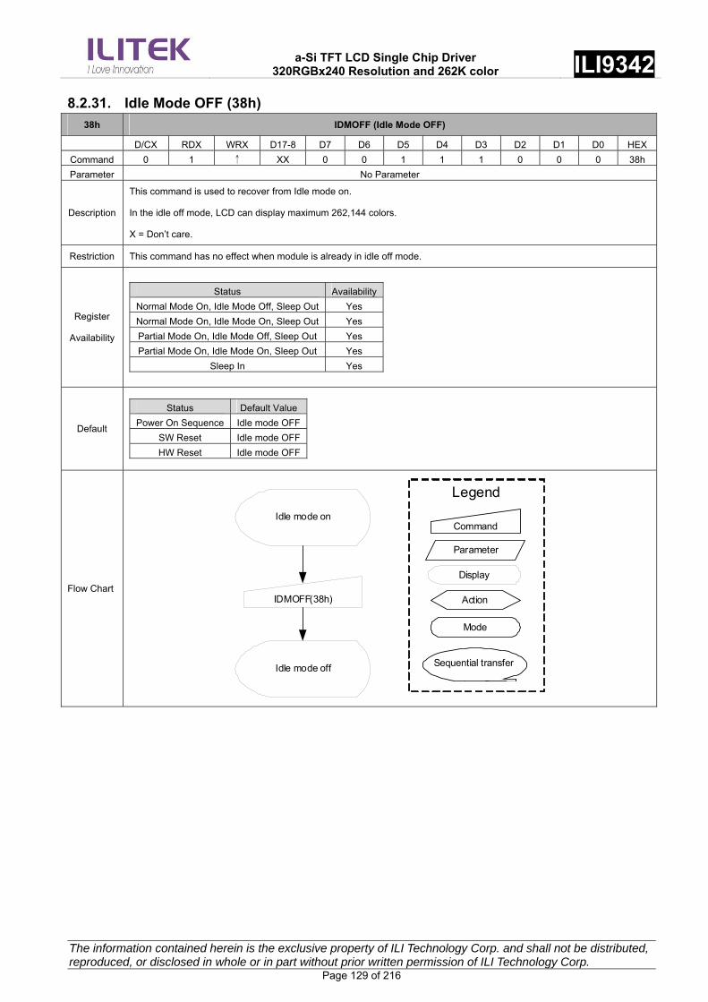
a-Si TFT LCD Single Chip Driver
320RGBx240 Resolution and 262K color ILI9342
The information contained herein is the exclusive property of ILI Technology Corp. and shall not be distributed, reproduced, or disclosed in whole or in part without prior written permission of ILI Technology Corp. Page 129 of 216
8.2.31. Idle Mode OFF (38h)
38h IDMOFF (Idle Mode OFF)
D/CX RDX WRX D17-8 D7 D6 D5 D4 D3 D2 D1 D0 HEX
Command 0 1 ↑ XX 0 0 1 1 1 0 0 0 38h
Parameter No Parameter
Description
This command is used to recover from Idle mode on.
In the idle off mode, LCD can display maximum 262,144 colors.
X = Don’t care.
Restriction This command has no effect when module is already in idle off mode.
Register
Availability
Status Availability
Normal Mode On, Idle Mode Off, Sleep Out Yes
Normal Mode On, Idle Mode On, Sleep Out Yes
Partial Mode On, Idle Mode Off, Sleep Out Yes
Partial Mode On, Idle Mode On, Sleep Out Yes
Sleep In Yes
Default
Status Default Value
Power On Sequence Idle mode OFF
SW Reset Idle mode OFF
HW Reset Idle mode OFF
Flow Chart
IDMOFF(38h)
Idle mode on
Idle mode off
Command
Parameter
Action
Mode
Legend
Sequential transfer
Display
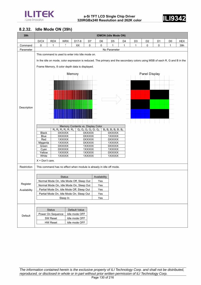
a-Si TFT LCD Single Chip Driver
320RGBx240 Resolution and 262K color ILI9342
The information contained herein is the exclusive property of ILI Technology Corp. and shall not be distributed, reproduced, or disclosed in whole or in part without prior written permission of ILI Technology Corp. Page 130 of 216
8.2.32. Idle Mode ON (39h)
39h IDMON (Idle Mode ON)
D/CX RDX WRX D17-8 D7 D6 D5 D4 D3 D2 D1 D0 HEX
Command 0 1 ↑ XX 0 0 1 1 1 0 0 1 39h
Parameter No Parameter
Description
This command is used to enter into Idle mode on.
In the idle on mode, color expression is reduced. The primary and the secondary colors using MSB of each R, G and B in the
Frame Memory, 8 color depth data is displayed.
Memory Panel Display
Memory Contents vs. Display Color
R5 R4 R3 R2 R1 R0 G5 G4 G3 G2 G1 G0 B5 B4 B3 B2 B1 B0
Black 0XXXXX 0XXXXX 0XXXXX Blue 0XXXXX 0XXXXX 1XXXXX Red 1XXXXX 0XXXXX 0XXXXX
Magenta 1XXXXX 0XXXXX 1XXXXX Green 0XXXXX 1XXXXX 0XXXXX Cyan 0XXXXX 1XXXXX 1XXXXX
Yellow 1XXXXX 1XXXXX 0XXXXX White 1XXXXX 1XXXXX 1XXXXX
X = Don’t care.
Restriction This command has no effect when module is already in idle off mode.
Register
Availability
Status Availability
Normal Mode On, Idle Mode Off, Sleep Out Yes
Normal Mode On, Idle Mode On, Sleep Out Yes
Partial Mode On, Idle Mode Off, Sleep Out Yes
Partial Mode On, Idle Mode On, Sleep Out Yes
Sleep In Yes
Default
Status Default Value
Power On Sequence Idle mode OFF
SW Reset Idle mode OFF
HW Reset Idle mode OFF
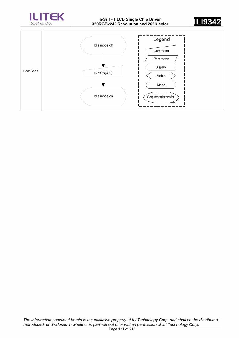
a-Si TFT LCD Single Chip Driver
320RGBx240 Resolution and 262K color ILI9342
The information contained herein is the exclusive property of ILI Technology Corp. and shall not be distributed, reproduced, or disclosed in whole or in part without prior written permission of ILI Technology Corp. Page 131 of 216
Flow Chart
IDMON(39h)
Idle mode off
Idle mode on
Command
Parameter
Action
Mode
Legend
Sequential transfer
Display

a-Si TFT LCD Single Chip Driver
320RGBx240 Resolution and 262K color ILI9342
The information contained herein is the exclusive property of ILI Technology Corp. and shall not be distributed, reproduced, or disclosed in whole or in part without prior written permission of ILI Technology Corp. Page 132 of 216
8.2.33. COLMOD: Pixel Format Set (3Ah)
3Ah PIXSET (Pixel Format Set)
D/CX RDX WRX D17-8 D7 D6 D5 D4 D3 D2 D1 D0 HEX
Command 0 1 ↑ XX 0 0 1 0 0 1 1 0 3Ah
Parameter 1 1 ↑ XX 0 DPI [2:0] 0 DBI [2:0] 66
Description
This command sets the pixel format for the RGB image data used by the interface. DPI [2:0] is the pixel format select of RGB
interface and DBI [2:0] is the pixel format of MPU interface. If a particular interface, either RGB interface or MPU interface, is
not used then the corresponding bits in the parameter are ignored. The pixel format is shown in the table below.
DPI [2:0] RGB Interface Format DBI [2:0] MPU Interface Format
0 0 0 Reserved 0 0 0 Reserved
0 0 1 Reserved 0 0 1 Reserved
0 1 0 Reserved 0 1 0 Reserved
0 1 1 12 bits / pixel 0 1 1 12 bits / pixel
1 0 0 Reserved 1 0 0 Reserved
1 0 1 16 bits / pixel 1 0 1 16 bits / pixel
1 1 0 18 bits / pixel 1 1 0 18 bits / pixel
1 1 1 Reserved 1 1 1 Reserved
X = Don’t care
Restriction
Register
Availability
Status Availability
Normal Mode On, Idle Mode Off, Sleep Out Yes
Normal Mode On, Idle Mode On, Sleep Out Yes
Partial Mode On, Idle Mode Off, Sleep Out Yes
Partial Mode On, Idle Mode On, Sleep Out Yes
Sleep In Yes
Default
Default Value Status
DPI [2:0] DBI [2:0]
Power On Sequence 3’b110 3’b110
SW Reset No Change No Change
HW Reset 3’b110 3’b110
Flow Chart
COLMOD (3Ah)
DPI[2:0] RGB pixel format DBI[2:0] MCU pixel format
Command
Parameter
Action
Mode
Legend
Sequential transfer
Display
Any Command
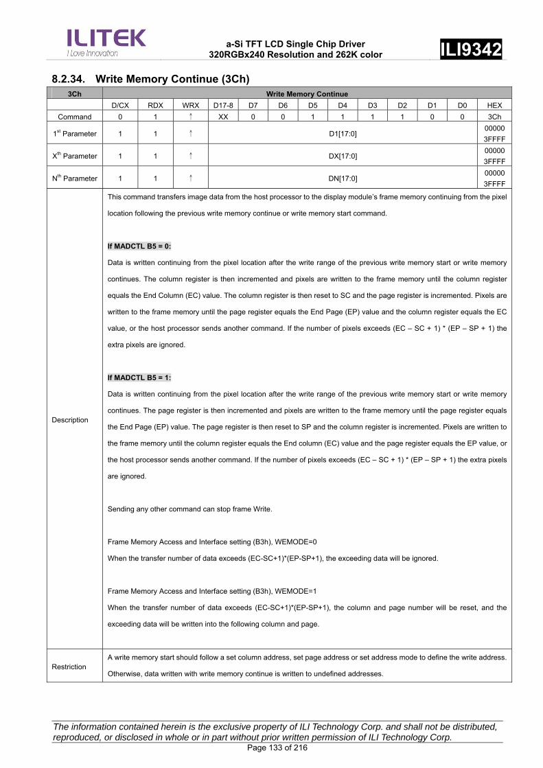
a-Si TFT LCD Single Chip Driver
320RGBx240 Resolution and 262K color ILI9342
The information contained herein is the exclusive property of ILI Technology Corp. and shall not be distributed, reproduced, or disclosed in whole or in part without prior written permission of ILI Technology Corp. Page 133 of 216
8.2.34. Write Memory Continue (3Ch) 3Ch Write Memory Continue
D/CX RDX WRX D17-8 D7 D6 D5 D4 D3 D2 D1 D0 HEX
Command 0 1 ↑ XX 0 0 1 1 1 1 0 0 3Ch
1st Parameter 1 1 ↑ D1[17:0] 00000
3FFFF
Xth Parameter 1 1 ↑ DX[17:0] 00000
3FFFF
Nth Parameter 1 1 ↑ DN[17:0] 00000
3FFFF
Description
This command transfers image data from the host processor to the display module’s frame memory continuing from the pixel
location following the previous write memory continue or write memory start command.
If MADCTL B5 = 0:
Data is written continuing from the pixel location after the write range of the previous write memory start or write memory
continues. The column register is then incremented and pixels are written to the frame memory until the column register
equals the End Column (EC) value. The column register is then reset to SC and the page register is incremented. Pixels are
written to the frame memory until the page register equals the End Page (EP) value and the column register equals the EC
value, or the host processor sends another command. If the number of pixels exceeds (EC – SC + 1) * (EP – SP + 1) the
extra pixels are ignored.
If MADCTL B5 = 1:
Data is written continuing from the pixel location after the write range of the previous write memory start or write memory
continues. The page register is then incremented and pixels are written to the frame memory until the page register equals
the End Page (EP) value. The page register is then reset to SP and the column register is incremented. Pixels are written to
the frame memory until the column register equals the End column (EC) value and the page register equals the EP value, or
the host processor sends another command. If the number of pixels exceeds (EC – SC + 1) * (EP – SP + 1) the extra pixels
are ignored.
Sending any other command can stop frame Write.
Frame Memory Access and Interface setting (B3h), WEMODE=0
When the transfer number of data exceeds (EC-SC+1)*(EP-SP+1), the exceeding data will be ignored.
Frame Memory Access and Interface setting (B3h), WEMODE=1
When the transfer number of data exceeds (EC-SC+1)*(EP-SP+1), the column and page number will be reset, and the
exceeding data will be written into the following column and page.
Restriction A write memory start should follow a set column address, set page address or set address mode to define the write address.
Otherwise, data written with write memory continue is written to undefined addresses.

a-Si TFT LCD Single Chip Driver
320RGBx240 Resolution and 262K color ILI9342
The information contained herein is the exclusive property of ILI Technology Corp. and shall not be distributed, reproduced, or disclosed in whole or in part without prior written permission of ILI Technology Corp. Page 134 of 216
Register
Availability
Status Availability
Normal Mode On, Idle Mode Off, Sleep Out Yes
Normal Mode On, Idle Mode On, Sleep Out Yes
Partial Mode On, Idle Mode Off, Sleep Out Yes
Partial Mode On, Idle Mode On, Sleep Out Yes
Sleep In No
Default
Status Default Value
Power On Sequence Random value
SW Reset No change
HW Reset No change
Flow Chart

a-Si TFT LCD Single Chip Driver
320RGBx240 Resolution and 262K color ILI9342
The information contained herein is the exclusive property of ILI Technology Corp. and shall not be distributed, reproduced, or disclosed in whole or in part without prior written permission of ILI Technology Corp. Page 135 of 216
8.2.35. Read Memory Continue (3Eh) 3Eh Read Memory Continue
D/CX RDX WRX D17-8 D7 D6 D5 D4 D3 D2 D1 D0 HEX
Command 0 1 ↑ XX 0 0 1 1 1 1 1 0 3Eh
1st Parameter 1 ↑ 1 XX X X X X X X X X X
2nd Parameter 1 ↑ 1 D1[17:0] 00000
3FFFF
xst Parameter 1 ↑ 1 DX[17:0] 00000
3FFFF
Nst Parameter 1 ↑ 1 DN[17:0] 00000
3FFFF
Description
This command transfers image data from the display module’s frame memory to the host processor continuing from the
location following the previous read memory continue (3Eh) or read memory start (2Eh) command.
If MADCTL B5 = 0:
Pixels are read continuing from the pixel location after the read range of the previous read memory start or read memory
continues. The column register is then incremented and pixels are read from the frame memory until the column register
equals the End Column (EC) value. The column register is then reset to SC and the page register is incremented. Pixels
are read from the frame memory until the page register equals the End Page (EP) value and the column register equals the
EC value, or the host processor sends another command.
If MADCTL B5 = 1:
Pixels are read continuing from the pixel location after the read range of the previous read memory start or read memory
continues. The page register is then incremented and pixels are read from the frame memory until the page register equals
the End Page (EP) value. The page register is then reset to SP and the column register is incremented. Pixels are read
from the frame memory until the column register equals the End Column (EC) value and the page register equals the EP
value, or the host processor sends another command.
This command makes no change to the other driver status.
Restriction A read memory start should follow a set column address, set page address or set address mode to define the read location.
Otherwise, data read with read memory continue is undefined.
Register
Availability
Status Availability
Normal Mode On, Idle Mode Off, Sleep Out Yes
Normal Mode On, Idle Mode On, Sleep Out Yes
Partial Mode On, Idle Mode Off, Sleep Out Yes
Partial Mode On, Idle Mode On, Sleep Out Yes
Sleep In Yes
Default
Status Default Value
Power On Sequence Random data
SW Reset No change
HW Reset No change
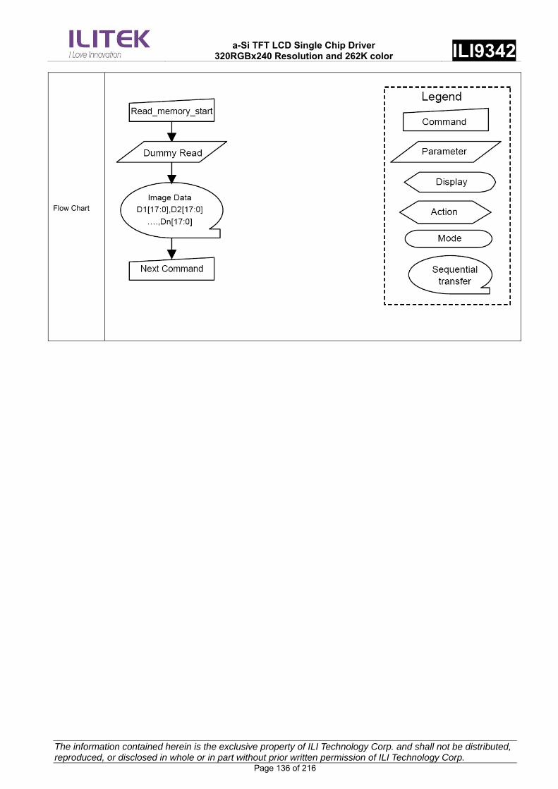
a-Si TFT LCD Single Chip Driver
320RGBx240 Resolution and 262K color ILI9342
The information contained herein is the exclusive property of ILI Technology Corp. and shall not be distributed, reproduced, or disclosed in whole or in part without prior written permission of ILI Technology Corp. Page 136 of 216
Flow Chart

a-Si TFT LCD Single Chip Driver
320RGBx240 Resolution and 262K color ILI9342
The information contained herein is the exclusive property of ILI Technology Corp. and shall not be distributed, reproduced, or disclosed in whole or in part without prior written permission of ILI Technology Corp. Page 137 of 216
8.2.36. Set Tear Scan line (44h) 44h Set Tear Scan line
D/CX RDX WRX D17-8 D7 D6 D5 D4 D3 D2 D1 D0 HEX
Command 0 1 ↑ XX 0 1 0 0 0 1 0 0 44h
1st Parameter 1 1 ↑ XX 0 0 0 0 0 0 0 STS[8] 00
2nd Parameter 1 1 ↑ XX STS[7:0] 00
Description
This command turns on the display Tearing Effect output signal on the TE signal line when the display reaches line N. The
TE signal is not affected by changing MADCTL bit B4. The Tearing Effect Line On has one parameter that describes the
Tearing Effect Output Line mode.
tvdl tvdh
Vertical Time Scale
Note that set tear scan line with N=0 is equivalent to set tear on with M=0.
The Tearing Effect Output line shall be active low when the display module is in Sleep mode.
Restriction -
Register
Availability
Status Availability
Normal Mode On, Idle Mode Off, Sleep Out Yes
Normal Mode On, Idle Mode On, Sleep Out Yes
Partial Mode On, Idle Mode Off, Sleep Out Yes
Partial Mode On, Idle Mode On, Sleep Out Yes
Sleep In Yes
Default
Status Default Value
Power On Sequence STS [8:0]=0000h
SW Reset STS [8:0]=0000h
HW Reset STS [8:0]=0000h
Flow Chart

a-Si TFT LCD Single Chip Driver
320RGBx240 Resolution and 262K color ILI9342
The information contained herein is the exclusive property of ILI Technology Corp. and shall not be distributed, reproduced, or disclosed in whole or in part without prior written permission of ILI Technology Corp. Page 138 of 216
8.2.37. Get Scan line (45h) 45h Get Scan line
D/CX RDX WRX D17-8 D7 D6 D5 D4 D3 D2 D1 D0 HEX
Command 0 1 ↑ XX 0 1 0 0 0 1 0 1 45h
1st Parameter 1 ↑ 1 XX X X X X X X X X X
2nd Parameter 1 ↑ 1 XX 0 0 0 0 0 0 GTS[9:8] 00
3rd Parameter 1 ↑ 1 XX GTS[7:0] 00
Description
The display returns the current scan line, N, used to update the display device. The total number of scan lines on a display
device is defined as VSYNC + VBP + VACT + VFP. The first scan line is defined as the first line of V-Sync and is denoted
as Line 0.
When in Sleep Mode, the value returned by get scan line is undefined.
Restriction None
Register
Availability
Status Availability
Normal Mode On, Idle Mode Off, Sleep Out Yes
Normal Mode On, Idle Mode On, Sleep Out Yes
Partial Mode On, Idle Mode Off, Sleep Out Yes
Partial Mode On, Idle Mode On, Sleep Out Yes
Sleep In Yes
Default
Default Value Status
GTS [9:0]
Power On Sequence GTS [9:0]=0000h
SW Reset GTS [9:0]=0000h
HW Reset GTS [9:0]=0000h
Flow Chart

a-Si TFT LCD Single Chip Driver
320RGBx240 Resolution and 262K color ILI9342
The information contained herein is the exclusive property of ILI Technology Corp. and shall not be distributed, reproduced, or disclosed in whole or in part without prior written permission of ILI Technology Corp. Page 139 of 216
8.2.38. Read ID1 (DAh)
DAh RDID1 (Read ID1)
D/CX RDX WRX D17-8 D7 D6 D5 D4 D3 D2 D1 D0 HEX
Command 0 1 ↑ XX 1 1 0 1 1 0 1 0 DAh
1stParameter 1 ↑ 1 XX X X X X X X X X X
2ndParameter 1 ↑ 1 XX ID1 [7:0] XX
Description
This read byte identifies the LCD module’s manufacturer ID and it is specified by User
The 1st parameter is dummy data.
The 2nd parameter is LCD module’s manufacturer ID.
X = Don’t care
Restriction
Register
Availability
Status Availability
Normal Mode On, Idle Mode Off, Sleep Out Yes
Normal Mode On, Idle Mode On, Sleep Out Yes
Partial Mode On, Idle Mode Off, Sleep Out Yes
Partial Mode On, Idle Mode On, Sleep Out Yes
Sleep In Yes
Default
Status Default Value
(Before MTP program)
Default Value
(After MTP program)
Power On Sequence 8’h00h MTP value
SW Reset 8’h00h MTP value
HW Reset 8’h00h MTP value
Flow Chart
Command
Parameter
Action
Mode
Legend
Sequential transfer
RDID1(DAh)
1st Parameter: Dummy Read2nd Parameter: Send ID1[7:0]
Host
Driver Display

a-Si TFT LCD Single Chip Driver
320RGBx240 Resolution and 262K color ILI9342
The information contained herein is the exclusive property of ILI Technology Corp. and shall not be distributed, reproduced, or disclosed in whole or in part without prior written permission of ILI Technology Corp. Page 140 of 216
8.2.39. Read ID2 (DBh)
DBh RDID2 (Read ID2)
D/CX RDX WRX D17-8 D7 D6 D5 D4 D3 D2 D1 D0 HEX
Command 0 1 ↑ XX 1 1 0 1 1 0 1 1 DBh
1st Parameter 1 ↑ 1 XX X X X X X X X X X
2ndParameter 1 ↑ 1 XX 1 ID2 [6:0] XX
Description
This read byte is used to track the LCD module/driver version. It is defined by display supplier (with User’s agreement) and
changes each time a revision is made to the display, material or construction specifications.
The 1st parameter is dummy data.
The 2nd parameter is LCD module/driver version ID and the ID parameter range is from 80h to FFh.
The ID2 can be programmed by MTP function.
X = Don’t care
Restriction
Register
Availability
Status Availability
Normal Mode On, Idle Mode Off, Sleep Out Yes
Normal Mode On, Idle Mode On, Sleep Out Yes
Partial Mode On, Idle Mode Off, Sleep Out Yes
Partial Mode On, Idle Mode On, Sleep Out Yes
Sleep In Yes
Default
Status Default Value
(Before MTP program)
Default Value
(After MTP program)
Power On Sequence 8’h80h MTP value
SW Reset 8’h80h MTP value
HW Reset 8’h80h MTP value
Flow Chart
Command
Parameter
Action
Mode
Legend
Sequential transfer
RDID2(DBh)
1st Parameter: Dummy Read2nd Parameter: Send ID2[7:0]
Host
Driver Display
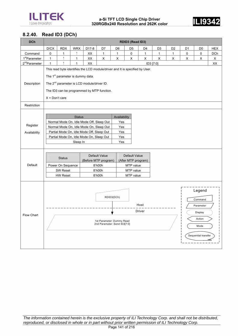
a-Si TFT LCD Single Chip Driver
320RGBx240 Resolution and 262K color ILI9342
The information contained herein is the exclusive property of ILI Technology Corp. and shall not be distributed, reproduced, or disclosed in whole or in part without prior written permission of ILI Technology Corp. Page 141 of 216
8.2.40. Read ID3 (DCh)
DCh RDID3 (Read ID3)
D/CX RDX WRX D17-8 D7 D6 D5 D4 D3 D2 D1 D0 HEX
Command 0 1 ↑ XX 1 1 0 1 1 1 0 0 DCh
1stParameter 1 ↑ 1 XX X X X X X X X X X
2ndParameter 1 ↑ 1 XX ID3 [7:0] XX
Description
This read byte identifies the LCD module/driver and It is specified by User.
The 1st parameter is dummy data.
The 2nd parameter is LCD module/driver ID.
The ID3 can be programmed by MTP function.
X = Don’t care
Restriction
Register
Availability
Status Availability
Normal Mode On, Idle Mode Off, Sleep Out Yes
Normal Mode On, Idle Mode On, Sleep Out Yes
Partial Mode On, Idle Mode Off, Sleep Out Yes
Partial Mode On, Idle Mode On, Sleep Out Yes
Sleep In Yes
Default
Status Default Value
(Before MTP program)
Default Value
(After MTP program)
Power On Sequence 8’h00h MTP value
SW Reset 8’h00h MTP value
HW Reset 8’h00h MTP value
Flow Chart
Command
Parameter
Action
Mode
Legend
Sequential transfer
RDID3(DCh)
1st Parameter: Dummy Read2nd Parameter: Send ID3[7:0]
Host
Driver Display
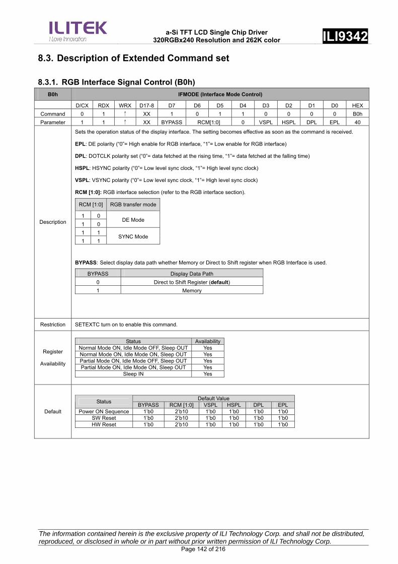
a-Si TFT LCD Single Chip Driver
320RGBx240 Resolution and 262K color ILI9342
The information contained herein is the exclusive property of ILI Technology Corp. and shall not be distributed, reproduced, or disclosed in whole or in part without prior written permission of ILI Technology Corp. Page 142 of 216
8.3. Description of Extended Command set
8.3.1. RGB Interface Signal Control (B0h)
B0h IFMODE (Interface Mode Control)
D/CX RDX WRX D17-8 D7 D6 D5 D4 D3 D2 D1 D0 HEX
Command 0 1 ↑ XX 1 0 1 1 0 0 0 0 B0h
Parameter 1 1 ↑ XX BYPASS RCM[1:0] 0 VSPL HSPL DPL EPL 40
Description
Sets the operation status of the display interface. The setting becomes effective as soon as the command is received.
EPL: DE polarity (“0”= High enable for RGB interface, “1”= Low enable for RGB interface)
DPL: DOTCLK polarity set (“0”= data fetched at the rising time, “1”= data fetched at the falling time)
HSPL: HSYNC polarity (“0”= Low level sync clock, “1”= High level sync clock)
VSPL: VSYNC polarity (“0”= Low level sync clock, “1”= High level sync clock)
RCM [1:0]: RGB interface selection (refer to the RGB interface section).
RCM [1:0] RGB transfer mode
1 0
1 0 DE Mode
1 1
1 1 SYNC Mode
BYPASS: Select display data path whether Memory or Direct to Shift register when RGB Interface is used.
BYPASS Display Data Path
0 Direct to Shift Register (default)
1 Memory
Restriction SETEXTC turn on to enable this command.
Register
Availability
Status AvailabilityNormal Mode ON, Idle Mode OFF, Sleep OUT Yes Normal Mode ON, Idle Mode ON, Sleep OUT Yes Partial Mode ON, Idle Mode OFF, Sleep OUT Yes Partial Mode ON, Idle Mode ON, Sleep OUT Yes
Sleep IN Yes
Default
Default Value Status
BYPASS RCM [1:0] VSPL HSPL DPL EPL Power ON Sequence 1’b0 2’b10 1’b0 1’b0 1’b0 1’b0
SW Reset 1’b0 2’b10 1’b0 1’b0 1’b0 1’b0 HW Reset 1’b0 2’b10 1’b0 1’b0 1’b0 1’b0
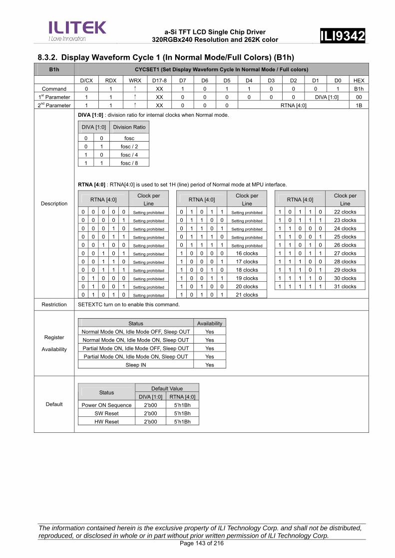
a-Si TFT LCD Single Chip Driver
320RGBx240 Resolution and 262K color ILI9342
The information contained herein is the exclusive property of ILI Technology Corp. and shall not be distributed, reproduced, or disclosed in whole or in part without prior written permission of ILI Technology Corp. Page 143 of 216
8.3.2. Display Waveform Cycle 1 (In Normal Mode/Full Colors) (B1h)
B1h CYCSET1 (Set Display Waveform Cycle In Normal Mode / Full colors)
D/CX RDX WRX D17-8 D7 D6 D5 D4 D3 D2 D1 D0 HEX
Command 0 1 ↑ XX 1 0 1 1 0 0 0 1 B1h
1st Parameter 1 1 ↑ XX 0 0 0 0 0 0 DIVA [1:0] 00
2nd Parameter 1 1 ↑ XX 0 0 0 RTNA [4:0] 1B
Description
DIVA [1:0] : division ratio for internal clocks when Normal mode.
DIVA [1:0] Division Ratio
0 0 fosc
0 1 fosc / 2
1 0 fosc / 4
1 1 fosc / 8
RTNA [4:0] : RTNA[4:0] is used to set 1H (line) period of Normal mode at MPU interface.
RTNA [4:0] Clock per
Line RTNA [4:0]
Clock per
Line RTNA [4:0]
Clock per
Line
0 0 0 0 0 Setting prohibited 0 1 0 1 1 Setting prohibited 1 0 1 1 0 22 clocks
0 0 0 0 1 Setting prohibited 0 1 1 0 0 Setting prohibited 1 0 1 1 1 23 clocks
0 0 0 1 0 Setting prohibited 0 1 1 0 1 Setting prohibited 1 1 0 0 0 24 clocks
0 0 0 1 1 Setting prohibited 0 1 1 1 0 Setting prohibited 1 1 0 0 1 25 clocks
0 0 1 0 0 Setting prohibited 0 1 1 1 1 Setting prohibited 1 1 0 1 0 26 clocks
0 0 1 0 1 Setting prohibited 1 0 0 0 0 16 clocks 1 1 0 1 1 27 clocks
0 0 1 1 0 Setting prohibited 1 0 0 0 1 17 clocks 1 1 1 0 0 28 clocks
0 0 1 1 1 Setting prohibited 1 0 0 1 0 18 clocks 1 1 1 0 1 29 clocks
0 1 0 0 0 Setting prohibited 1 0 0 1 1 19 clocks 1 1 1 1 0 30 clocks
0 1 0 0 1 Setting prohibited 1 0 1 0 0 20 clocks 1 1 1 1 1 31 clocks
0 1 0 1 0 Setting prohibited
1 0 1 0 1 21 clocks
Restriction SETEXTC turn on to enable this command.
Register
Availability
Status Availability
Normal Mode ON, Idle Mode OFF, Sleep OUT Yes
Normal Mode ON, Idle Mode ON, Sleep OUT Yes
Partial Mode ON, Idle Mode OFF, Sleep OUT Yes
Partial Mode ON, Idle Mode ON, Sleep OUT Yes
Sleep IN Yes
Default
Default Value Status
DIVA [1:0] RTNA [4:0]
Power ON Sequence 2’b00 5’h1Bh
SW Reset 2’b00 5’h1Bh
HW Reset 2’b00 5’h1Bh

a-Si TFT LCD Single Chip Driver
320RGBx240 Resolution and 262K color ILI9342
The information contained herein is the exclusive property of ILI Technology Corp. and shall not be distributed, reproduced, or disclosed in whole or in part without prior written permission of ILI Technology Corp. Page 144 of 216
8.3.3. Display Waveform Cycle 2 (In Idle Mode/8 colors) (B2h)
B2h CYCSET2 (Set Display Waveform Cycle In Idle Mode / 8 colors)
D/CX RDX WRX D17-8 D7 D6 D5 D4 D3 D2 D1 D0 HEX
Command 0 1 ↑ XX 1 0 1 1 0 0 1 0 B2h
1st Parameter 1 1 ↑ XX 0 0 0 0 0 0 DIVB [1:0] 00
2ndParameter 1 1 ↑ XX 0 0 0 RTNB [4:0] 1B
Description
DIVB [1:0]: division ratio for internal clocks when Idle mode.
DIVB [1:0] Division Ratio
0 0 fosc
0 1 fosc / 2
1 0 fosc / 4
1 1 fosc / 8
RTNB [4:0]: RTNB[4:0] is used to set 1H (line) period of Idle mode at MPU interface.
RTNB [4:0] Clock per
Line RTNB [4:0]
Clock per
Line RTNB [4:0]
Clock per
Line
0 0 0 0 0 Setting prohibited 0 1 0 1 1 Setting prohibited 1 0 1 1 0 22 clocks
0 0 0 0 1 Setting prohibited 0 1 1 0 0 Setting prohibited 1 0 1 1 1 23 clocks
0 0 0 1 0 Setting prohibited 0 1 1 0 1 Setting prohibited 1 1 0 0 0 24 clocks
0 0 0 1 1 Setting prohibited 0 1 1 1 0 Setting prohibited 1 1 0 0 1 25 clocks
0 0 1 0 0 Setting prohibited 0 1 1 1 1 Setting prohibited 1 1 0 1 0 26 clocks
0 0 1 0 1 Setting prohibited 1 0 0 0 0 16 clocks 1 1 0 1 1 27 clocks
0 0 1 1 0 Setting prohibited 1 0 0 0 1 17 clocks 1 1 1 0 0 28 clocks
0 0 1 1 1 Setting prohibited 1 0 0 1 0 18 clocks 1 1 1 0 1 29 clocks
0 1 0 0 0 Setting prohibited 1 0 0 1 1 19 clocks 1 1 1 1 0 30 clocks
0 1 0 0 1 Setting prohibited 1 0 1 0 0 20 clocks 1 1 1 1 1 31 clocks
0 1 0 1 0 Setting prohibited
1 0 1 0 1 21 clocks
Restriction SETEXTC turn on to enable this command.
Register
Availability
Status Availability
Normal Mode ON, Idle Mode OFF, Sleep OUT Yes
Normal Mode ON, Idle Mode ON, Sleep OUT Yes
Partial Mode ON, Idle Mode OFF, Sleep OUT Yes
Partial Mode ON, Idle Mode ON, Sleep OUT Yes
Sleep IN Yes
Default
Default Value Status
DIVB [1:0] RTNB [4:0]
Power ON Sequence 2’b00 5’h1Bh
SW Reset 2’b00 5’h1Bh
HW Reset 2’b00 5’h1Bh

a-Si TFT LCD Single Chip Driver
320RGBx240 Resolution and 262K color ILI9342
The information contained herein is the exclusive property of ILI Technology Corp. and shall not be distributed, reproduced, or disclosed in whole or in part without prior written permission of ILI Technology Corp. Page 145 of 216
8.3.4. Display Waveform Cycle (In Partial Mode/Full Colors) (B3h)
B3h CYCSET3 (Set Display Waveform Cycle In Partial Mode / Full colors)
D/CX RDX WRX D17-8 D7 D6 D5 D4 D3 D2 D1 D0 HEX
Command 0 1 ↑ XX 1 0 1 1 0 0 1 1 B3h
1st Parameter 1 1 ↑ XX 0 0 0 0 0 0 DIVC [1:0] 00
2ndParameter 1 1 ↑ XX 0 0 0 RTNC [4:0] 1B
Description
DIVC [1:0]: division ratio for internal clocks when Partial mode.
DIVC [1:0] Division Ratio
0 0 fosc
0 1 fosc / 2
1 0 fosc / 4
1 1 fosc / 8
RTNC [4:0]: RTNC [4:0] is used to set 1H (line) period of Partial mode at MPU interface.
RTNC [4:0] Clock per
Line RTNC [4:0]
Clock per
Line RTNC [4:0]
Clock per
Line
0 0 0 0 0 Setting prohibited 0 1 0 1 1 Setting prohibited 1 0 1 1 0 22 clocks
0 0 0 0 1 Setting prohibited 0 1 1 0 0 Setting prohibited 1 0 1 1 1 23 clocks
0 0 0 1 0 Setting prohibited 0 1 1 0 1 Setting prohibited 1 1 0 0 0 24 clocks
0 0 0 1 1 Setting prohibited 0 1 1 1 0 Setting prohibited 1 1 0 0 1 25 clocks
0 0 1 0 0 Setting prohibited 0 1 1 1 1 Setting prohibited 1 1 0 1 0 26 clocks
0 0 1 0 1 Setting prohibited 1 0 0 0 0 16 clocks 1 1 0 1 1 27 clocks
0 0 1 1 0 Setting prohibited 1 0 0 0 1 17 clocks 1 1 1 0 0 28 clocks
0 0 1 1 1 Setting prohibited 1 0 0 1 0 18 clocks 1 1 1 0 1 29 clocks
0 1 0 0 0 Setting prohibited 1 0 0 1 1 19 clocks 1 1 1 1 0 30 clocks
0 1 0 0 1 Setting prohibited 1 0 1 0 0 20 clocks 1 1 1 1 1 31 clocks
0 1 0 1 0 Setting prohibited
1 0 1 0 1 21 clocks
Restriction SETEXTC turn on to enable this command.
Register
Availability
Status Availability
Normal Mode ON, Idle Mode OFF, Sleep OUT Yes
Normal Mode ON, Idle Mode ON, Sleep OUT Yes
Partial Mode ON, Idle Mode OFF, Sleep OUT Yes
Partial Mode ON, Idle Mode ON, Sleep OUT Yes
Sleep IN Yes
Default
Default Value Status
DIVC [1:0] RTNC [4:0]
Power ON Sequence 2’b00 5’h1Bh
SW Reset 2’b00 5’h1Bh
HW Reset 2’b00 5’h1Bh
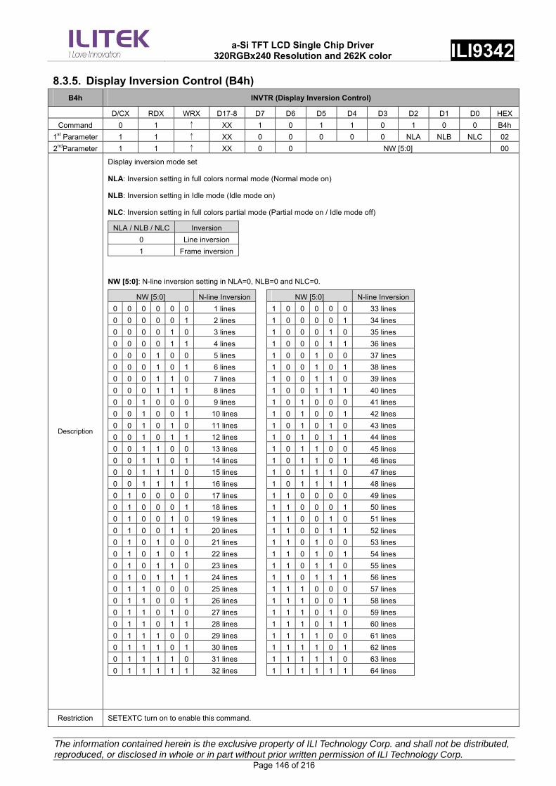
a-Si TFT LCD Single Chip Driver
320RGBx240 Resolution and 262K color ILI9342
The information contained herein is the exclusive property of ILI Technology Corp. and shall not be distributed, reproduced, or disclosed in whole or in part without prior written permission of ILI Technology Corp. Page 146 of 216
8.3.5. Display Inversion Control (B4h)
B4h INVTR (Display Inversion Control)
D/CX RDX WRX D17-8 D7 D6 D5 D4 D3 D2 D1 D0 HEX
Command 0 1 ↑ XX 1 0 1 1 0 1 0 0 B4h
1st Parameter 1 1 ↑ XX 0 0 0 0 0 NLA NLB NLC 02
2ndParameter 1 1 ↑ XX 0 0 NW [5:0] 00
Description
Display inversion mode set
NLA: Inversion setting in full colors normal mode (Normal mode on)
NLB: Inversion setting in Idle mode (Idle mode on)
NLC: Inversion setting in full colors partial mode (Partial mode on / Idle mode off)
NLA / NLB / NLC Inversion
0 Line inversion
1 Frame inversion
NW [5:0]: N-line inversion setting in NLA=0, NLB=0 and NLC=0.
NW [5:0] N-line Inversion NW [5:0] N-line Inversion
0 0 0 0 0 0 1 lines 1 0 0 0 0 0 33 lines
0 0 0 0 0 1 2 lines 1 0 0 0 0 1 34 lines
0 0 0 0 1 0 3 lines 1 0 0 0 1 0 35 lines
0 0 0 0 1 1 4 lines 1 0 0 0 1 1 36 lines
0 0 0 1 0 0 5 lines 1 0 0 1 0 0 37 lines
0 0 0 1 0 1 6 lines 1 0 0 1 0 1 38 lines
0 0 0 1 1 0 7 lines 1 0 0 1 1 0 39 lines
0 0 0 1 1 1 8 lines 1 0 0 1 1 1 40 lines
0 0 1 0 0 0 9 lines 1 0 1 0 0 0 41 lines
0 0 1 0 0 1 10 lines 1 0 1 0 0 1 42 lines
0 0 1 0 1 0 11 lines 1 0 1 0 1 0 43 lines
0 0 1 0 1 1 12 lines 1 0 1 0 1 1 44 lines
0 0 1 1 0 0 13 lines 1 0 1 1 0 0 45 lines
0 0 1 1 0 1 14 lines 1 0 1 1 0 1 46 lines
0 0 1 1 1 0 15 lines 1 0 1 1 1 0 47 lines
0 0 1 1 1 1 16 lines 1 0 1 1 1 1 48 lines
0 1 0 0 0 0 17 lines 1 1 0 0 0 0 49 lines
0 1 0 0 0 1 18 lines 1 1 0 0 0 1 50 lines
0 1 0 0 1 0 19 lines 1 1 0 0 1 0 51 lines
0 1 0 0 1 1 20 lines 1 1 0 0 1 1 52 lines
0 1 0 1 0 0 21 lines 1 1 0 1 0 0 53 lines
0 1 0 1 0 1 22 lines 1 1 0 1 0 1 54 lines
0 1 0 1 1 0 23 lines 1 1 0 1 1 0 55 lines
0 1 0 1 1 1 24 lines 1 1 0 1 1 1 56 lines
0 1 1 0 0 0 25 lines 1 1 1 0 0 0 57 lines
0 1 1 0 0 1 26 lines 1 1 1 0 0 1 58 lines
0 1 1 0 1 0 27 lines 1 1 1 0 1 0 59 lines
0 1 1 0 1 1 28 lines 1 1 1 0 1 1 60 lines
0 1 1 1 0 0 29 lines 1 1 1 1 0 0 61 lines
0 1 1 1 0 1 30 lines 1 1 1 1 0 1 62 lines
0 1 1 1 1 0 31 lines 1 1 1 1 1 0 63 lines
0 1 1 1 1 1 32 lines 1 1 1 1 1 1 64 lines
Restriction SETEXTC turn on to enable this command.

a-Si TFT LCD Single Chip Driver
320RGBx240 Resolution and 262K color ILI9342
The information contained herein is the exclusive property of ILI Technology Corp. and shall not be distributed, reproduced, or disclosed in whole or in part without prior written permission of ILI Technology Corp. Page 147 of 216
Register
Availability
Status Availability
Normal Mode ON, Idle Mode OFF, Sleep OUT Yes
Normal Mode ON, Idle Mode ON, Sleep OUT Yes
Partial Mode ON, Idle Mode OFF, Sleep OUT Yes
Partial Mode ON, Idle Mode ON, Sleep OUT Yes
Sleep IN Yes
Default
Default Value Status
NLA NLB NLC NW [5:0]
Power ON Sequence 1’b0 1’b1 1’b0 6’h00h
SW Reset 1’b0 1’b1 1’b0 6’h00h
H/W Reset 1’b0 1’b1 1’b0 6’h00h
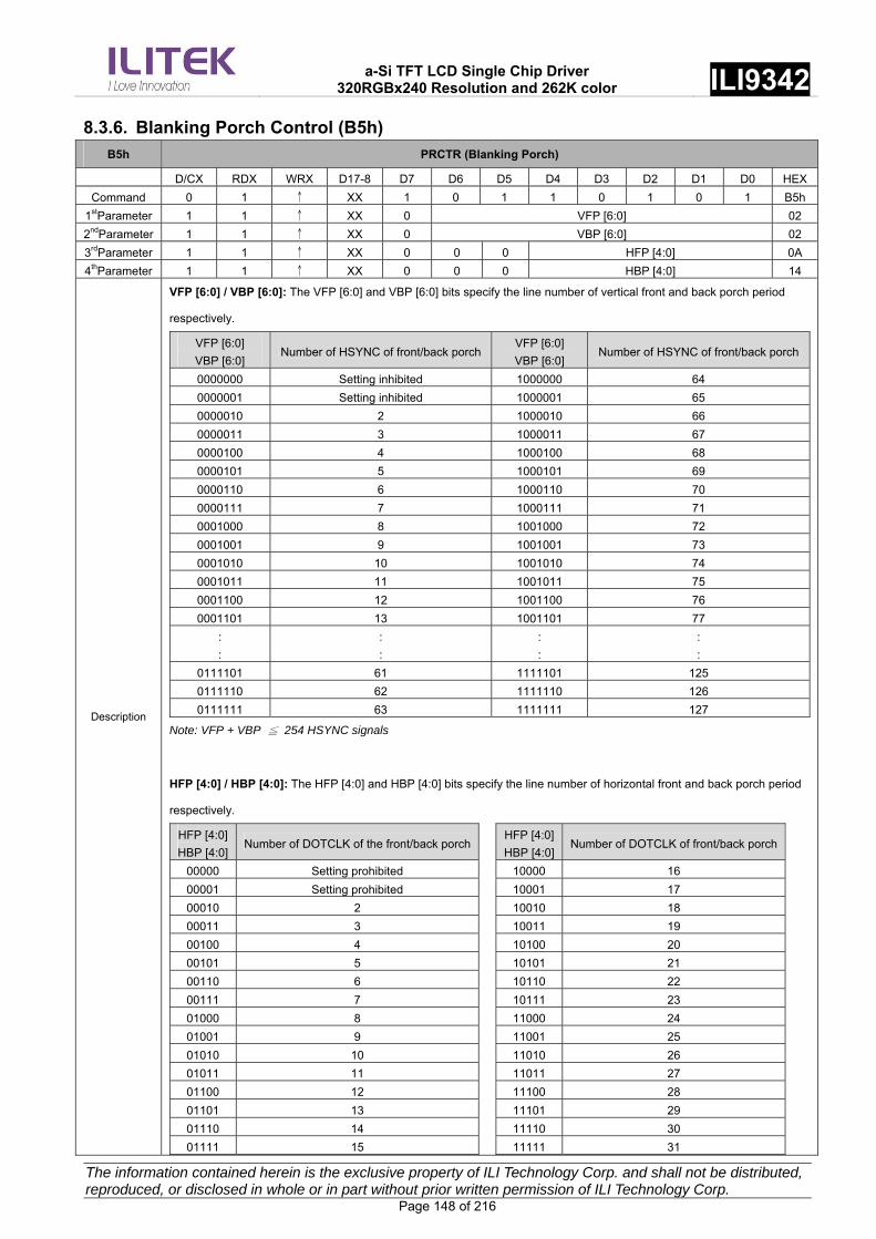
a-Si TFT LCD Single Chip Driver
320RGBx240 Resolution and 262K color ILI9342
The information contained herein is the exclusive property of ILI Technology Corp. and shall not be distributed, reproduced, or disclosed in whole or in part without prior written permission of ILI Technology Corp. Page 148 of 216
8.3.6. Blanking Porch Control (B5h)
B5h PRCTR (Blanking Porch)
D/CX RDX WRX D17-8 D7 D6 D5 D4 D3 D2 D1 D0 HEX
Command 0 1 ↑ XX 1 0 1 1 0 1 0 1 B5h
1stParameter 1 1 ↑ XX 0 VFP [6:0] 02
2ndParameter 1 1 ↑ XX 0 VBP [6:0] 02
3rdParameter 1 1 ↑ XX 0 0 0 HFP [4:0] 0A
4thParameter 1 1 ↑ XX 0 0 0 HBP [4:0] 14
Description
VFP [6:0] / VBP [6:0]: The VFP [6:0] and VBP [6:0] bits specify the line number of vertical front and back porch period
respectively.
VFP [6:0]
VBP [6:0] Number of HSYNC of front/back porch
VFP [6:0]
VBP [6:0] Number of HSYNC of front/back porch
0000000 Setting inhibited 1000000 64
0000001 Setting inhibited 1000001 65
0000010 2 1000010 66
0000011 3 1000011 67
0000100 4 1000100 68
0000101 5 1000101 69
0000110 6 1000110 70
0000111 7 1000111 71
0001000 8 1001000 72
0001001 9 1001001 73
0001010 10 1001010 74
0001011 11 1001011 75
0001100 12 1001100 76
0001101 13 1001101 77
:
:
:
:
:
:
:
:
0111101 61 1111101 125
0111110 62 1111110 126
0111111 63 1111111 127
Note: VFP + VBP ≦ 254 HSYNC signals
HFP [4:0] / HBP [4:0]: The HFP [4:0] and HBP [4:0] bits specify the line number of horizontal front and back porch period
respectively.
HFP [4:0]
HBP [4:0] Number of DOTCLK of the front/back porch
HFP [4:0]
HBP [4:0]Number of DOTCLK of front/back porch
00000 Setting prohibited 10000 16
00001 Setting prohibited 10001 17
00010 2 10010 18
00011 3 10011 19
00100 4 10100 20
00101 5 10101 21
00110 6 10110 22
00111 7 10111 23
01000 8 11000 24
01001 9 11001 25
01010 10 11010 26
01011 11 11011 27
01100 12 11100 28
01101 13 11101 29
01110 14 11110 30
01111 15 11111 31

a-Si TFT LCD Single Chip Driver
320RGBx240 Resolution and 262K color ILI9342
The information contained herein is the exclusive property of ILI Technology Corp. and shall not be distributed, reproduced, or disclosed in whole or in part without prior written permission of ILI Technology Corp. Page 149 of 216
Restriction SETEXTC turn on to enable this command.
Register
Availability
Status Availability
Normal Mode ON, Idle Mode OFF, Sleep OUT Yes
Normal Mode ON, Idle Mode ON, Sleep OUT Yes
Partial Mode ON, Idle Mode OFF, Sleep OUT Yes
Partial Mode ON, Idle Mode ON, Sleep OUT Yes
Sleep IN Yes
Default
Default Value Status
VFP [6:0] VBP [6:0] HFP [4:0] HBP [4:0]
Power ON Sequence 7’h02h 7’h02h 5’h0Ah 5’h14h
SW Reset 7’h02h 7’h02h 5’h0Ah 5’h14h
HW Reset 7’h02h 7’h02h 5’h0Ah 5’h14h

a-Si TFT LCD Single Chip Driver
320RGBx240 Resolution and 262K color ILI9342
The information contained herein is the exclusive property of ILI Technology Corp. and shall not be distributed, reproduced, or disclosed in whole or in part without prior written permission of ILI Technology Corp. Page 150 of 216
8.3.7. Display Function Control (B6h)
B6h DISCTRL (Display Function Control)
D/CX RDX WRX D17-8 D7 D6 D5 D4 D3 D2 D1 D0 HEX
Command 0 1 ↑ XX 1 0 1 1 0 1 1 0 B6h
1st Parameter 1 1 ↑ XX 0 0 0 0 PTG [1:0] PT [1:0] 0A
2nd Parameter 1 1 ↑ XX REV GS SS SM ISC [3:0] 02
3rd Parameter 1 1 ↑ XX 0 0 NL [5:0] 27
4th Parameter 1 1 ↑ XX X X PCDIV[5:0] 04
Description
PTG [1:0]: Set the scan mode in non-display area.
PTG1 PTG0 Gate outputs in non-display area Source outputs in non-display area VCOM output
0 0 Normal scan Set with the PT [2:0] bits VCOMH/VCOML
0 1 Setting prohibited --- ---
1 0 Interval scan Set with the PT [2:0] bits
1 1 Setting prohibited --- ---
PT [1:0]: Determine source/VCOM output in a non-display area in the partial display mode.
Source output on non-display area VCOM output on non-display area PT [1:0]
Positive polarity Negative polarity Positive polarity Negative polarity
0 0 V63 V0 VCOML VCOMH
0 1 V0 V63 VCOML VCOMH
1 0 AGND AGND AGND AGND
1 1 Hi-Z Hi-Z AGND AGND
SS: This bit controls MPU to memory write/read direction by column address order.
REV: Select whether the liquid crystal type is normally white type or normally black type.
REV Liquid crystal type
0 Normally black
1 Normally white
ISC [3:0]: Specify the scan cycle interval of gate driver in non-display area when PTG [1:0] =”10” to select interval scan.
Then scan cycle is set as odd number from 0~29 frame periods. The polarity is inverted every scan cycle.
ISC [3:0] Scan Cycle fFLM = 60Hz
0000 1 frame 17ms
0001 3 frames 51ms
0010 5 frames 85ms
0011 7 frames 119ms
0100 9 frames 153ms
0101 11 frames 187ms
0110 13 frames 221ms
0111 15 frames 255ms
1000 17 frames 289ms
1001 19 frames 323ms
1010 21 frames 357ms
1011 23 frames 391ms
1100 25 frames 425ms
1101 27 frames 459ms
1110 29 frames 493ms
1111 31 frames 527ms
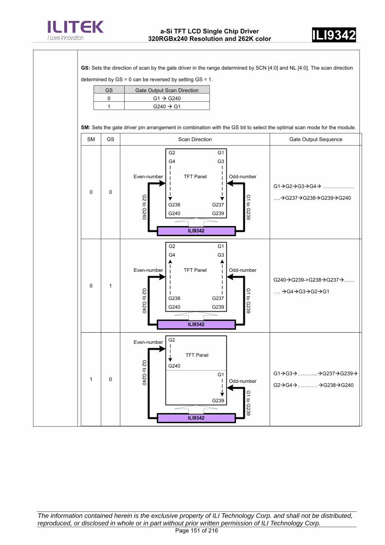
a-Si TFT LCD Single Chip Driver
320RGBx240 Resolution and 262K color ILI9342
The information contained herein is the exclusive property of ILI Technology Corp. and shall not be distributed, reproduced, or disclosed in whole or in part without prior written permission of ILI Technology Corp. Page 151 of 216
GS: Sets the direction of scan by the gate driver in the range determined by SCN [4:0] and NL [4:0]. The scan direction
determined by GS = 0 can be reversed by setting GS = 1.
GS Gate Output Scan Direction
0 G1 G240
1 G240 G1
SM: Sets the gate driver pin arrangement in combination with the GS bit to select the optimal scan mode for the module.
SM GS Scan Direction Gate Output Sequence
0 0
G4
G2
G240
G238
G3
G1
G239
G237
ILI9342
Even-number Odd-number
G2 to
G2
40
G1 to
G2
39
TFT Panel
G1G2G3G4 ………………
….G237G238G239G240
0 1
ILI9342
Even-number Odd-number
G2 to
G2
40
G1 to
G2
39
G4
G2
G240
G238
G3
G1
G239
G237
TFT Panel
G240G239->G238G237……
…. G4G3G2G1
1 0
G240
G2
G1
ILI9342
Odd-number
Even-number
G2
to G24
0
G1 to
G2
39
G239
TFT Panel
G1G3………...G237G239
G2G4…………G238G240

a-Si TFT LCD Single Chip Driver
320RGBx240 Resolution and 262K color ILI9342
The information contained herein is the exclusive property of ILI Technology Corp. and shall not be distributed, reproduced, or disclosed in whole or in part without prior written permission of ILI Technology Corp. Page 152 of 216
1 1
G240
G2
G1
ILI9342
Odd-number
Even-number
G2
to G24
0
G1 to
G239
G239
TFT Panel
G240, G238, G236, …,
G10, G8, G6, G4, G2
G239, G237, G235, …,
G9, G78, G5, G3, G1
G240G238………...G4G2
G239G237…………G3G1
NL [5:0]: Sets the number of lines to drive the LCD at an interval of 8 lines. The GRAM address mapping is not affected
by the number of lines set by NL [5:0]. The number of lines must be the same or more than the number of lines necessary
for the size of the liquid crystal panel.
NL [5:0] LCD Drive Line NL [5:0] LCD Driver Line 0 0 0 0 0 0 Setting prohibited 0 1 0 1 0 1 176 lines 0 0 0 0 0 1 16 lines 0 1 0 1 1 0 184 lines 0 0 0 0 1 0 24 lines 0 1 0 1 1 1 192 lines 0 0 0 0 1 1 32 lines 0 1 1 0 0 0 200 lines 0 0 0 1 0 0 40 lines 0 1 1 0 0 1 208 lines 0 0 0 1 0 1 48 lines 0 1 1 0 1 0 216 lines 0 0 0 1 1 0 56 lines 0 1 1 0 1 1 224 lines 0 0 0 1 1 1 64 lines 0 1 1 1 0 0 232 lines 0 0 1 0 0 0 72 lines 0 1 1 1 0 1 240 lines 0 1 0 0 1 1 160 lines Others Setting inhibited 0 1 0 1 0 0 168 lines
PCDIVH [3:0]: Number of DOTCLK during internal clock CLKD’s high period. In units of 1 clock.
PCDIVL [3:0]: Number of DOTCLK during internal clock CLKD’s low period. In units of 1 clock.
PCDIVH and PCDIVL, specifying DOTCLK’s division ratio, are determined so that difference between PCLKD’s
frequency and internal oscillation clock 678KHz is the smallest. Set PCDIVL = PCDIVH or PCDIVL - 1.
DOTCLK
PCLKD
PCDIVH[3:0] PCDIVL[3:0]
1)PCDIVL
PCDIVH( 2
DOTCLK
foscExternal
Restriction SETEXTC turn on to enable this command.

a-Si TFT LCD Single Chip Driver
320RGBx240 Resolution and 262K color ILI9342
The information contained herein is the exclusive property of ILI Technology Corp. and shall not be distributed, reproduced, or disclosed in whole or in part without prior written permission of ILI Technology Corp. Page 153 of 216
Register
Availability
Status Availability
Normal Mode ON, Idle Mode OFF, Sleep OUT Yes
Normal Mode ON, Idle Mode ON, Sleep OUT Yes
Partial Mode ON, Idle Mode OFF, Sleep OUT Yes
Partial Mode ON, Idle Mode ON, Sleep OUT Yes
Sleep IN Yes
Default
Default Value Status
PTG [1:0] PT [1:0] REV GS SS SM ISC [3:0] NL [5:0]
Power ON Sequence 2’b10 2’b10 1’b0 1’b0 1’b0 1’b0 4’b0010 6’h27h
SW Reset 2’b10 2’b10 1’b0 1’b0 1’b0 1’b0 4’b0010 6’h27h
HW Reset 2’b10 2’b10 1’b0 1’b0 1’b0 1’b0 4’b0010 6’h27h

a-Si TFT LCD Single Chip Driver
320RGBx240 Resolution and 262K color ILI9342
The information contained herein is the exclusive property of ILI Technology Corp. and shall not be distributed, reproduced, or disclosed in whole or in part without prior written permission of ILI Technology Corp. Page 154 of 216
8.3.8. Entry Mode Set (B7h)
B7h ETMOD (Entry Mode Set)
D/CX RDX WRX D17-8 D7 D6 D5 D4 D3 D2 D1 D0 HEX
Command 0 1 ↑ XX 1 0 1 1 0 1 1 1 B7h
Parameter 1 1 ↑ XX 0 0 0 0 DSTB GON DTE GAS 07
Description
DSTB: The ILI9342 driver enters the Deep Standby Mode when DSTB is set to high (“1”). In Deep Standby mode, both
internal logic power and SRAM power are turn off, the display data stored in the Frame Memory and the instructions are not
saved. Rewrite Frame Memory content and instructions after the Deep Standby Mode is exited.
Note: ILI9342 provides two ways to exit the Deep Standby Mode:
(1) Exit Deep Standby Mode by pull down CSX to low (“0”) 6 times.
(2) Input a RESX pulse with effective low level duration to start up the inside logic regulator and makes a transition
to the initial state.
CSX
WRX
RDX
D/CX
D[17:0]
1 32 4 5 6Wait 1ms or more
“High”
Don Care
“Low” or “High”
“High”
Don Care Don Care Don Care Don Care Don Care
GAS: Low voltage detection control.
GAS Low voltage detection
0 Enable
1 Disable
GON/DTE: Set the output level of gate driver G1 ~ G240 as follows
GON DTE G1~G240 Gate Output
0 0 VGH
0 1 VGH
1 0 VGL
1 1 Normal display
Restriction SETEXTC turn on to enable this command.
Register
Availability
Status Availability
Normal Mode ON, Idle Mode OFF, Sleep OUT Yes
Normal Mode ON, Idle Mode ON, Sleep OUT Yes
Partial Mode ON, Idle Mode OFF, Sleep OUT Yes
Partial Mode ON, Idle Mode ON, Sleep OUT Yes
Sleep IN Yes
Default
Default Value Status
DSTB GON DTE GAS
Power ON Sequence 1’b0 1’b1 1’b1 1’b1
SW Reset 1’b0 1’b1 1’b1 1’b1
HW Reset 1’b0 1’b1 1’b1 1’b1
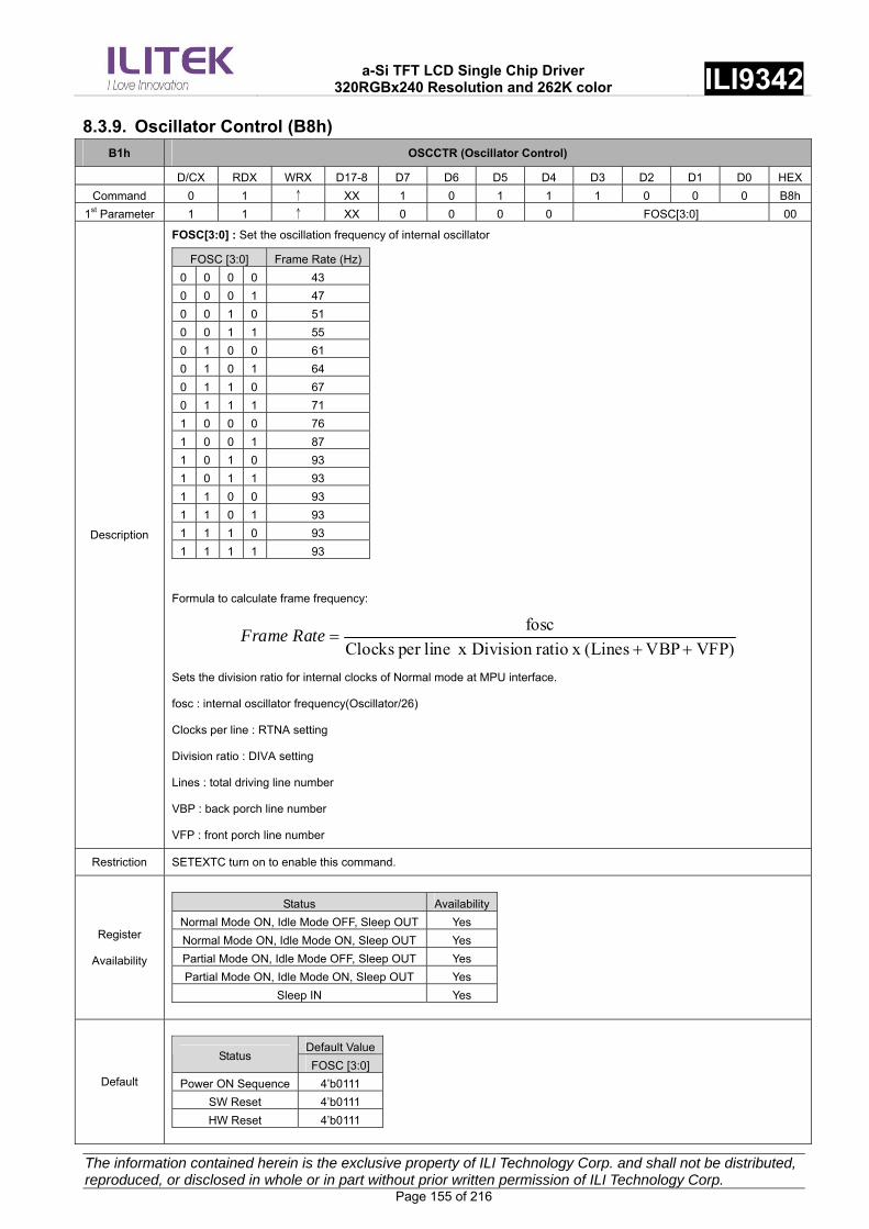
a-Si TFT LCD Single Chip Driver
320RGBx240 Resolution and 262K color ILI9342
The information contained herein is the exclusive property of ILI Technology Corp. and shall not be distributed, reproduced, or disclosed in whole or in part without prior written permission of ILI Technology Corp. Page 155 of 216
8.3.9. Oscillator Control (B8h)
B1h OSCCTR (Oscillator Control)
D/CX RDX WRX D17-8 D7 D6 D5 D4 D3 D2 D1 D0 HEX
Command 0 1 ↑ XX 1 0 1 1 1 0 0 0 B8h
1st Parameter 1 1 ↑ XX 0 0 0 0 FOSC[3:0] 00
Description
FOSC[3:0] : Set the oscillation frequency of internal oscillator
FOSC [3:0] Frame Rate (Hz)
0 0 0 0 43
0 0 0 1 47
0 0 1 0 51
0 0 1 1 55
0 1 0 0 61
0 1 0 1 64
0 1 1 0 67
0 1 1 1 71
1 0 0 0 76
1 0 0 1 87
1 0 1 0 93
1 0 1 1 93
1 1 0 0 93
1 1 0 1 93
1 1 1 0 93
1 1 1 1 93
Formula to calculate frame frequency:
VFP)VBP (Lines x ratioDivision x lineper Clocks
fosc
RateFrame
Sets the division ratio for internal clocks of Normal mode at MPU interface.
fosc : internal oscillator frequency(Oscillator/26)
Clocks per line : RTNA setting
Division ratio : DIVA setting
Lines : total driving line number
VBP : back porch line number
VFP : front porch line number
Restriction SETEXTC turn on to enable this command.
Register
Availability
Status Availability
Normal Mode ON, Idle Mode OFF, Sleep OUT Yes
Normal Mode ON, Idle Mode ON, Sleep OUT Yes
Partial Mode ON, Idle Mode OFF, Sleep OUT Yes
Partial Mode ON, Idle Mode ON, Sleep OUT Yes
Sleep IN Yes
Default
Default ValueStatus
FOSC [3:0]
Power ON Sequence 4’b0111
SW Reset 4’b0111
HW Reset 4’b0111
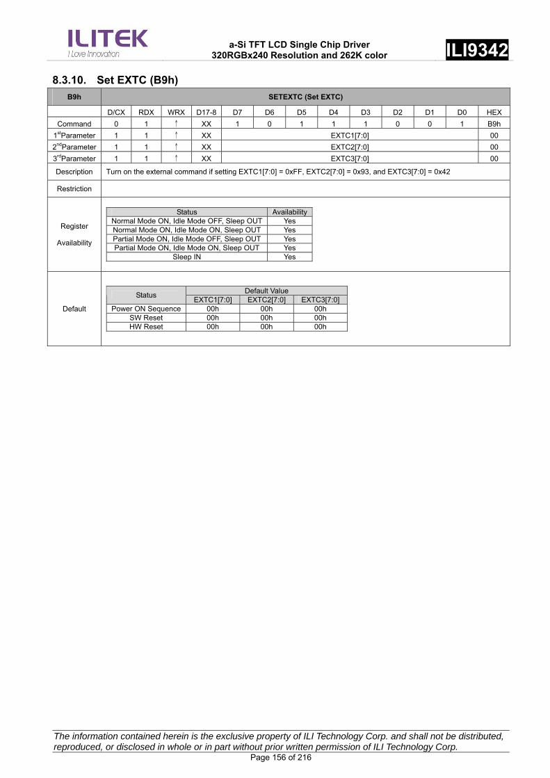
a-Si TFT LCD Single Chip Driver
320RGBx240 Resolution and 262K color ILI9342
The information contained herein is the exclusive property of ILI Technology Corp. and shall not be distributed, reproduced, or disclosed in whole or in part without prior written permission of ILI Technology Corp. Page 156 of 216
8.3.10. Set EXTC (B9h)
B9h SETEXTC (Set EXTC)
D/CX RDX WRX D17-8 D7 D6 D5 D4 D3 D2 D1 D0 HEX
Command 0 1 ↑ XX 1 0 1 1 1 0 0 1 B9h
1stParameter 1 1 ↑ XX EXTC1[7:0] 00
2ndParameter 1 1 ↑ XX EXTC2[7:0] 00
3rdParameter 1 1 ↑ XX EXTC3[7:0] 00
Description Turn on the external command if setting EXTC1[7:0] = 0xFF, EXTC2[7:0] = 0x93, and EXTC3[7:0] = 0x42
Restriction
Register
Availability
Status AvailabilityNormal Mode ON, Idle Mode OFF, Sleep OUT Yes Normal Mode ON, Idle Mode ON, Sleep OUT Yes Partial Mode ON, Idle Mode OFF, Sleep OUT Yes Partial Mode ON, Idle Mode ON, Sleep OUT Yes
Sleep IN Yes
Default
Default Value Status
EXTC1[7:0] EXTC2[7:0] EXTC3[7:0]Power ON Sequence 00h 00h 00h
SW Reset 00h 00h 00h HW Reset 00h 00h 00h
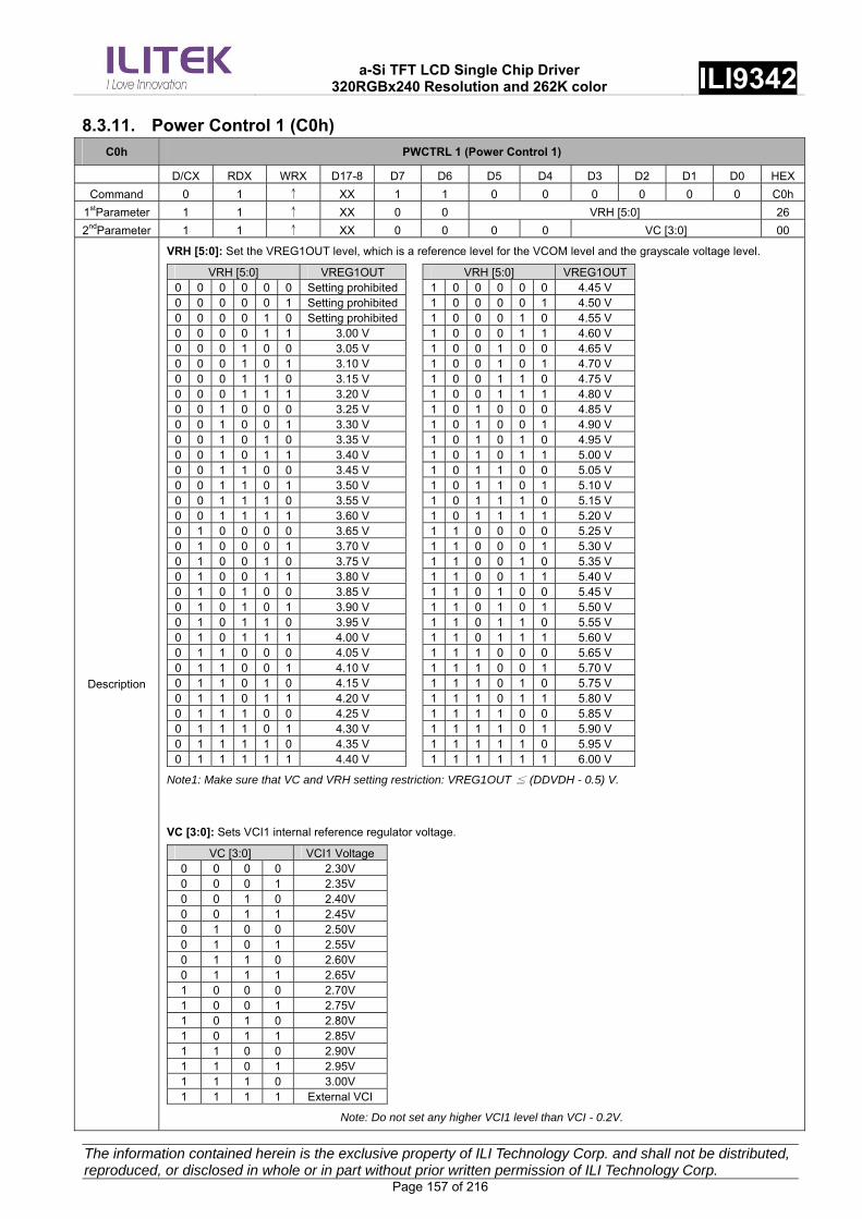
a-Si TFT LCD Single Chip Driver
320RGBx240 Resolution and 262K color ILI9342
The information contained herein is the exclusive property of ILI Technology Corp. and shall not be distributed, reproduced, or disclosed in whole or in part without prior written permission of ILI Technology Corp. Page 157 of 216
8.3.11. Power Control 1 (C0h)
C0h PWCTRL 1 (Power Control 1)
D/CX RDX WRX D17-8 D7 D6 D5 D4 D3 D2 D1 D0 HEX
Command 0 1 ↑ XX 1 1 0 0 0 0 0 0 C0h
1stParameter 1 1 ↑ XX 0 0 VRH [5:0] 26
2ndParameter 1 1 ↑ XX 0 0 0 0 VC [3:0] 00
Description
VRH [5:0]: Set the VREG1OUT level, which is a reference level for the VCOM level and the grayscale voltage level.
VRH [5:0] VREG1OUT VRH [5:0] VREG1OUT 0 0 0 0 0 0 Setting prohibited 1 0 0 0 0 0 4.45 V
0 0 0 0 0 1 Setting prohibited 1 0 0 0 0 1 4.50 V
0 0 0 0 1 0 Setting prohibited 1 0 0 0 1 0 4.55 V
0 0 0 0 1 1 3.00 V 1 0 0 0 1 1 4.60 V
0 0 0 1 0 0 3.05 V 1 0 0 1 0 0 4.65 V
0 0 0 1 0 1 3.10 V 1 0 0 1 0 1 4.70 V
0 0 0 1 1 0 3.15 V 1 0 0 1 1 0 4.75 V
0 0 0 1 1 1 3.20 V 1 0 0 1 1 1 4.80 V
0 0 1 0 0 0 3.25 V 1 0 1 0 0 0 4.85 V
0 0 1 0 0 1 3.30 V 1 0 1 0 0 1 4.90 V
0 0 1 0 1 0 3.35 V 1 0 1 0 1 0 4.95 V
0 0 1 0 1 1 3.40 V 1 0 1 0 1 1 5.00 V
0 0 1 1 0 0 3.45 V 1 0 1 1 0 0 5.05 V
0 0 1 1 0 1 3.50 V 1 0 1 1 0 1 5.10 V
0 0 1 1 1 0 3.55 V 1 0 1 1 1 0 5.15 V
0 0 1 1 1 1 3.60 V 1 0 1 1 1 1 5.20 V
0 1 0 0 0 0 3.65 V 1 1 0 0 0 0 5.25 V
0 1 0 0 0 1 3.70 V 1 1 0 0 0 1 5.30 V
0 1 0 0 1 0 3.75 V 1 1 0 0 1 0 5.35 V
0 1 0 0 1 1 3.80 V 1 1 0 0 1 1 5.40 V
0 1 0 1 0 0 3.85 V 1 1 0 1 0 0 5.45 V
0 1 0 1 0 1 3.90 V 1 1 0 1 0 1 5.50 V
0 1 0 1 1 0 3.95 V 1 1 0 1 1 0 5.55 V
0 1 0 1 1 1 4.00 V 1 1 0 1 1 1 5.60 V
0 1 1 0 0 0 4.05 V 1 1 1 0 0 0 5.65 V
0 1 1 0 0 1 4.10 V 1 1 1 0 0 1 5.70 V
0 1 1 0 1 0 4.15 V 1 1 1 0 1 0 5.75 V
0 1 1 0 1 1 4.20 V 1 1 1 0 1 1 5.80 V
0 1 1 1 0 0 4.25 V 1 1 1 1 0 0 5.85 V
0 1 1 1 0 1 4.30 V 1 1 1 1 0 1 5.90 V
0 1 1 1 1 0 4.35 V 1 1 1 1 1 0 5.95 V
0 1 1 1 1 1 4.40 V 1 1 1 1 1 1 6.00 V
Note1: Make sure that VC and VRH setting restriction: VREG1OUT ≦ (DDVDH - 0.5) V.
VC [3:0]: Sets VCI1 internal reference regulator voltage.
VC [3:0] VCI1 Voltage0 0 0 0 2.30V 0 0 0 1 2.35V 0 0 1 0 2.40V 0 0 1 1 2.45V 0 1 0 0 2.50V 0 1 0 1 2.55V 0 1 1 0 2.60V 0 1 1 1 2.65V 1 0 0 0 2.70V 1 0 0 1 2.75V 1 0 1 0 2.80V 1 0 1 1 2.85V 1 1 0 0 2.90V 1 1 0 1 2.95V 1 1 1 0 3.00V 1 1 1 1 External VCI
Note: Do not set any higher VCI1 level than VCI - 0.2V.
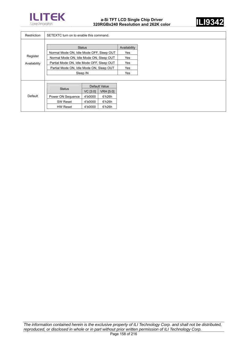
a-Si TFT LCD Single Chip Driver
320RGBx240 Resolution and 262K color ILI9342
The information contained herein is the exclusive property of ILI Technology Corp. and shall not be distributed, reproduced, or disclosed in whole or in part without prior written permission of ILI Technology Corp. Page 158 of 216
Restriction SETEXTC turn on to enable this command.
Register
Availability
Status Availability
Normal Mode ON, Idle Mode OFF, Sleep OUT Yes
Normal Mode ON, Idle Mode ON, Sleep OUT Yes
Partial Mode ON, Idle Mode OFF, Sleep OUT Yes
Partial Mode ON, Idle Mode ON, Sleep OUT Yes
Sleep IN Yes
Default
Default Value Status
VC [3:0] VRH [5:0]
Power ON Sequence 4’b0000 6’h26h
SW Reset 4’b0000 6’h26h
HW Reset 4’b0000 6’h26h

a-Si TFT LCD Single Chip Driver
320RGBx240 Resolution and 262K color ILI9342
The information contained herein is the exclusive property of ILI Technology Corp. and shall not be distributed, reproduced, or disclosed in whole or in part without prior written permission of ILI Technology Corp. Page 159 of 216
8.3.12. Power Control 2 (C1h)
C1h PWCTRL 2 (Power Control 2)
D/CX RDX WRX D17-8 D7 D6 D5 D4 D3 D2 D1 D0 HEX
Command 0 1 ↑ XX 1 1 0 0 0 0 0 1 C1h
Parameter 1 1 ↑ XX 0 SAP [2:0] BT [3:0] 10
Description
BT [3:0]: Sets the factor used in the step-up circuits.
Select the optimal step-up factor for the operating voltage. To reduce power consumption, set a smaller factor.
BT [3:0] DDVDH VGH VGL
0 0 0 0 -VCI1 x 5
0 0 0 1 -VCI1 x 4
0 0 1 0
VCI1 x 6
-VCI1 x 3
0 0 1 1 -VCI1 x 5
0 1 0 0 -VCI1 x 4
0 1 0 1
VCI1 x 5
-VCI1 x 3
0 1 1 0 -VCI1 x 4
0 1 1 1
VCI1 x 2
VCI1 x 4 -VCI1 x 3
1 0 0 0 -VCI1 x 7
1 0 0 1 -VCI1 x 6
1 0 1 0
VCI1 x 9
-VCI1 x 4
1 0 1 1 -VCI1 x 7
1 1 0 0 -VCI1 x 6
1 1 0 1
VCI1 x 7
-VCI1 x 4
1 1 1 0 -VCI1 x 6
1 1 1 1
VCI1 x 3
VCI1 x 6 -VCI1 x 4
Note1: Make sure that DDVDH setting restriction: DDVDH ≦ 6.0 V.
2: Make sure that VGH and VGL setting restriction: VGH -VGL ≦ 32 V.
SAP[2:0]: Adjusts the constant current in the operational amplifier circuit in the LCD power supply circuit. The larger
constant current enhances the drivability of the LCD, but it also increases the current consumption. Adjust the constant
current taking the trade-off into account between the display quality and the current consumption. In no-display period, set
SAP[2:0] = “000” to halt the operational amplifier circuits and the step-up circuits to reduce current consumption.
SAP[2:0] Gamma driver amplifiers Source driver amplifiers
000 Halt Halt
001 1.00 1.00
010 1.00 0.75
011 1.00 0.50
100 0.75 1.00
101 0.75 0.75
110 0.75 0.50
111 0.50 0.50
Restriction SETEXTC turn on to enable this command.
Register
Availability
Status Availability
Normal Mode ON, Idle Mode OFF, Sleep OUT Yes
Normal Mode ON, Idle Mode ON, Sleep OUT Yes
Partial Mode ON, Idle Mode OFF, Sleep OUT Yes
Partial Mode ON, Idle Mode ON, Sleep OUT Yes
Sleep IN Yes

a-Si TFT LCD Single Chip Driver
320RGBx240 Resolution and 262K color ILI9342
The information contained herein is the exclusive property of ILI Technology Corp. and shall not be distributed, reproduced, or disclosed in whole or in part without prior written permission of ILI Technology Corp. Page 160 of 216
Default
Default Value Status
BT [3:0] SAP [2:0]
Power ON Sequence 4’b0000 3’b001
SW Reset 4’b0000 3’b001
HW Reset 4’b0000 3’b001
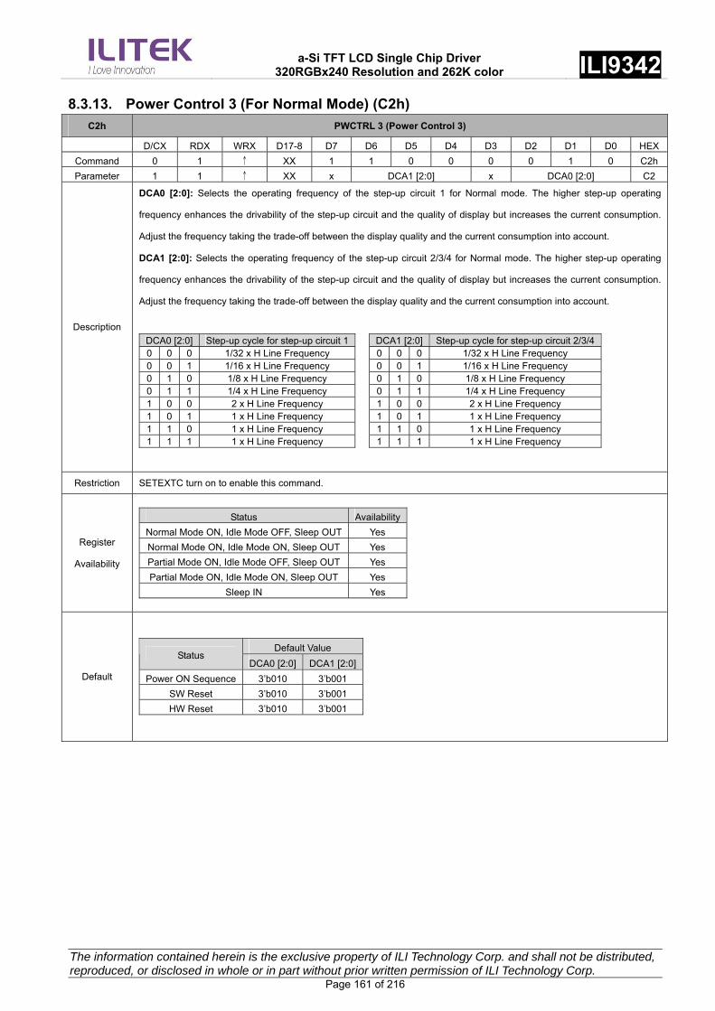
a-Si TFT LCD Single Chip Driver
320RGBx240 Resolution and 262K color ILI9342
The information contained herein is the exclusive property of ILI Technology Corp. and shall not be distributed, reproduced, or disclosed in whole or in part without prior written permission of ILI Technology Corp. Page 161 of 216
8.3.13. Power Control 3 (For Normal Mode) (C2h)
C2h PWCTRL 3 (Power Control 3)
D/CX RDX WRX D17-8 D7 D6 D5 D4 D3 D2 D1 D0 HEX
Command 0 1 ↑ XX 1 1 0 0 0 0 1 0 C2h
Parameter 1 1 ↑ XX x DCA1 [2:0] x DCA0 [2:0] C2
Description
DCA0 [2:0]: Selects the operating frequency of the step-up circuit 1 for Normal mode. The higher step-up operating
frequency enhances the drivability of the step-up circuit and the quality of display but increases the current consumption.
Adjust the frequency taking the trade-off between the display quality and the current consumption into account.
DCA1 [2:0]: Selects the operating frequency of the step-up circuit 2/3/4 for Normal mode. The higher step-up operating
frequency enhances the drivability of the step-up circuit and the quality of display but increases the current consumption.
Adjust the frequency taking the trade-off between the display quality and the current consumption into account.
DCA0 [2:0] Step-up cycle for step-up circuit 1 DCA1 [2:0] Step-up cycle for step-up circuit 2/3/40 0 0 1/32 x H Line Frequency 0 0 0 1/32 x H Line Frequency 0 0 1 1/16 x H Line Frequency 0 0 1 1/16 x H Line Frequency 0 1 0 1/8 x H Line Frequency 0 1 0 1/8 x H Line Frequency 0 1 1 1/4 x H Line Frequency 0 1 1 1/4 x H Line Frequency 1 0 0 2 x H Line Frequency 1 0 0 2 x H Line Frequency 1 0 1 1 x H Line Frequency 1 0 1 1 x H Line Frequency 1 1 0 1 x H Line Frequency 1 1 0 1 x H Line Frequency 1 1 1 1 x H Line Frequency 1 1 1 1 x H Line Frequency
Restriction SETEXTC turn on to enable this command.
Register
Availability
Status Availability
Normal Mode ON, Idle Mode OFF, Sleep OUT Yes
Normal Mode ON, Idle Mode ON, Sleep OUT Yes
Partial Mode ON, Idle Mode OFF, Sleep OUT Yes
Partial Mode ON, Idle Mode ON, Sleep OUT Yes
Sleep IN Yes
Default
Default Value Status
DCA0 [2:0] DCA1 [2:0]
Power ON Sequence 3’b010 3’b001
SW Reset 3’b010 3’b001
HW Reset 3’b010 3’b001

a-Si TFT LCD Single Chip Driver
320RGBx240 Resolution and 262K color ILI9342
The information contained herein is the exclusive property of ILI Technology Corp. and shall not be distributed, reproduced, or disclosed in whole or in part without prior written permission of ILI Technology Corp. Page 162 of 216
8.3.14. Power Control 4 (For Idle Mode) (C3h)
C3h PWCTRL 4 (Power Control 4)
D/CX RDX WRX D17-8 D7 D6 D5 D4 D3 D2 D1 D0 HEX
Command 0 1 ↑ XX 1 1 0 0 0 0 1 1 C3h
Parameter 1 1 ↑ XX X DCB1 [2:0] X DCB0 [2:0] C2
Description
DCB0 [2:0]: Selects the operating frequency of the step-up circuit 1 for Idle mode. The higher step-up operating frequency
enhances the drivability of the step-up circuit and the quality of display but increases the current consumption. Adjust the
frequency taking the trade-off between the display quality and the current consumption into account.
DCB1 [2:0]: Selects the operating frequency of the step-up circuit 2/3/4 for Idle mode. The higher step-up operating
frequency enhances the drivability of the step-up circuit and the quality of display but increases the current consumption.
Adjust the frequency taking the trade-off between the display quality and the current consumption into account.
DCB0 [2:0] Step-up cycle for step-up circuit 1 DCB1 [2:0] Step-up cycle for step-up circuit 2/3/40 0 0 1/32 x H Line Frequency 0 0 0 1/32 x H Line Frequency 0 0 1 1/16 x H Line Frequency 0 0 1 1/16 x H Line Frequency 0 1 0 1/8 x H Line Frequency 0 1 0 1/8 x H Line Frequency 0 1 1 1/4 x H Line Frequency 0 1 1 1/4 x H Line Frequency 1 0 0 2 x H Line Frequency 1 0 0 2 x H Line Frequency 1 0 1 1 x H Line Frequency 1 0 1 1 x H Line Frequency 1 1 0 1 x H Line Frequency 1 1 0 1 x H Line Frequency 1 1 1 1 x H Line Frequency 1 1 1 1 x H Line Frequency
Restriction SETEXTC turn on to enable this command.
Register
Availability
Status Availability
Normal Mode ON, Idle Mode OFF, Sleep OUT Yes
Normal Mode ON, Idle Mode ON, Sleep OUT Yes
Partial Mode ON, Idle Mode OFF, Sleep OUT Yes
Partial Mode ON, Idle Mode ON, Sleep OUT Yes
Sleep IN Yes
Default
Default Value Status
DCB0 [2:0] DCB1 [2:0]
Power ON Sequence 3’b010 3’b001
SW Reset 3’b010 3’b001
H/W Reset 3’b010 3’b001

a-Si TFT LCD Single Chip Driver
320RGBx240 Resolution and 262K color ILI9342
The information contained herein is the exclusive property of ILI Technology Corp. and shall not be distributed, reproduced, or disclosed in whole or in part without prior written permission of ILI Technology Corp. Page 163 of 216
8.3.15. Power Control 5 (For Partial Mode) (C4h)
C4h PWCTRL 5 (Power Control 5)
D/CX RDX WRX D17-8 D7 D6 D5 D4 D3 D2 D1 D0 HEX
Command 0 1 ↑ XX 1 1 0 0 0 1 0 0 C4h
Parameter 1 1 ↑ XX X DCC1 [2:0] X DCC0 [2:0] C2
Description
DCC0 [2:0]: Selects the operating frequency of the step-up circuit 1 for Partial mode. The higher step-up operating
frequency enhances the drivability of the step-up circuit and the quality of display but increases the current consumption.
Adjust the frequency taking the trade-off between the display quality and the current consumption into account.
DCC1 [2:0]: Selects the operating frequency of the step-up circuit 2/3/4 for Partial mode. The higher step-up operating
frequency enhances the drivability of the step-up circuit and the quality of display but increases the current consumption.
Adjust the frequency taking the trade-off between the display quality and the current consumption into account.
DCC0 [2:0] Step-up cycle for step-up circuit 1 DCC1 [2:0] Step-up cycle for step-up circuit 2/3/40 0 0 1/32 x H Line Frequency 0 0 0 1/32 x H Line Frequency 0 0 1 1/16 x H Line Frequency 0 0 1 1/16 x H Line Frequency 0 1 0 1/8 x H Line Frequency 0 1 0 1/8 x H Line Frequency 0 1 1 1/4 x H Line Frequency 0 1 1 1/4 x H Line Frequency 1 0 0 2 x H Line Frequency 1 0 0 2 x H Line Frequency 1 0 1 1 x H Line Frequency 1 0 1 1 x H Line Frequency 1 1 0 1 x H Line Frequency 1 1 0 1 x H Line Frequency 1 1 1 1 x H Line Frequency 1 1 1 1 x H Line Frequency
Restriction SETEXTC turn on to enable this command.
Register
Availability
Status Availability
Normal Mode ON, Idle Mode OFF, Sleep OUT Yes
Normal Mode ON, Idle Mode ON, Sleep OUT Yes
Partial Mode ON, Idle Mode OFF, Sleep OUT Yes
Partial Mode ON, Idle Mode ON, Sleep OUT Yes
Sleep IN Yes
Default
Default Value Status
DCC0 [2:0] DCC1 [2:0]
Power ON Sequence 3’b010 3’b001
SW Reset 3’b010 3’b001
HW Reset 3’b010 3’b001
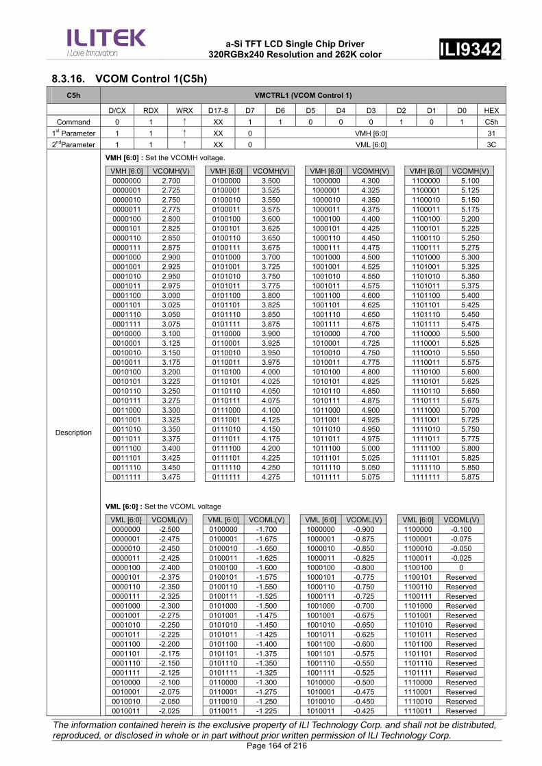
a-Si TFT LCD Single Chip Driver
320RGBx240 Resolution and 262K color ILI9342
The information contained herein is the exclusive property of ILI Technology Corp. and shall not be distributed, reproduced, or disclosed in whole or in part without prior written permission of ILI Technology Corp. Page 164 of 216
8.3.16. VCOM Control 1(C5h)
C5h VMCTRL1 (VCOM Control 1)
D/CX RDX WRX D17-8 D7 D6 D5 D4 D3 D2 D1 D0 HEX
Command 0 1 ↑ XX 1 1 0 0 0 1 0 1 C5h
1st Parameter 1 1 ↑ XX 0 VMH [6:0] 31
2ndParameter 1 1 ↑ XX 0 VML [6:0] 3C
Description
VMH [6:0] : Set the VCOMH voltage.
VMH [6:0] VCOMH(V) VMH [6:0] VCOMH(V) VMH [6:0] VCOMH(V) VMH [6:0] VCOMH(V)0000000 2.700 0100000 3.500 1000000 4.300 1100000 5.100
0000001 2.725 0100001 3.525 1000001 4.325 1100001 5.125
0000010 2.750 0100010 3.550 1000010 4.350 1100010 5.150
0000011 2.775 0100011 3.575 1000011 4.375 1100011 5.175
0000100 2.800 0100100 3.600 1000100 4.400 1100100 5.200
0000101 2.825 0100101 3.625 1000101 4.425 1100101 5.225
0000110 2.850 0100110 3.650 1000110 4.450 1100110 5.250
0000111 2.875 0100111 3.675 1000111 4.475 1100111 5.275
0001000 2.900 0101000 3.700 1001000 4.500 1101000 5.300
0001001 2.925 0101001 3.725 1001001 4.525 1101001 5.325
0001010 2.950 0101010 3.750 1001010 4.550 1101010 5.350
0001011 2.975 0101011 3.775 1001011 4.575 1101011 5.375
0001100 3.000 0101100 3.800 1001100 4.600 1101100 5.400
0001101 3.025 0101101 3.825 1001101 4.625 1101101 5.425
0001110 3.050 0101110 3.850 1001110 4.650 1101110 5.450
0001111 3.075 0101111 3.875 1001111 4.675 1101111 5.475
0010000 3.100 0110000 3.900 1010000 4.700 1110000 5.500
0010001 3.125 0110001 3.925 1010001 4.725 1110001 5.525
0010010 3.150 0110010 3.950 1010010 4.750 1110010 5.550
0010011 3.175 0110011 3.975 1010011 4.775 1110011 5.575
0010100 3.200 0110100 4.000 1010100 4.800 1110100 5.600
0010101 3.225 0110101 4.025 1010101 4.825 1110101 5.625
0010110 3.250 0110110 4.050 1010110 4.850 1110110 5.650
0010111 3.275 0110111 4.075 1010111 4.875 1110111 5.675
0011000 3.300 0111000 4.100 1011000 4.900 1111000 5.700
0011001 3.325 0111001 4.125 1011001 4.925 1111001 5.725
0011010 3.350 0111010 4.150 1011010 4.950 1111010 5.750
0011011 3.375 0111011 4.175 1011011 4.975 1111011 5.775
0011100 3.400 0111100 4.200 1011100 5.000 1111100 5.800
0011101 3.425 0111101 4.225 1011101 5.025 1111101 5.825
0011110 3.450 0111110 4.250 1011110 5.050 1111110 5.850
0011111 3.475
0111111 4.275 1011111 5.075
1111111 5.875
VML [6:0] : Set the VCOML voltage
VML [6:0] VCOML(V) VML [6:0] VCOML(V) VML [6:0] VCOML(V) VML [6:0] VCOML(V)0000000 -2.500 0100000 -1.700 1000000 -0.900 1100000 -0.100
0000001 -2.475 0100001 -1.675 1000001 -0.875 1100001 -0.075
0000010 -2.450 0100010 -1.650 1000010 -0.850 1100010 -0.050
0000011 -2.425 0100011 -1.625 1000011 -0.825 1100011 -0.025
0000100 -2.400 0100100 -1.600 1000100 -0.800 1100100 0
0000101 -2.375 0100101 -1.575 1000101 -0.775 1100101 Reserved0000110 -2.350 0100110 -1.550 1000110 -0.750 1100110 Reserved0000111 -2.325 0100111 -1.525 1000111 -0.725 1100111 Reserved0001000 -2.300 0101000 -1.500 1001000 -0.700 1101000 Reserved0001001 -2.275 0101001 -1.475 1001001 -0.675 1101001 Reserved0001010 -2.250 0101010 -1.450 1001010 -0.650 1101010 Reserved0001011 -2.225 0101011 -1.425 1001011 -0.625 1101011 Reserved0001100 -2.200 0101100 -1.400 1001100 -0.600 1101100 Reserved0001101 -2.175 0101101 -1.375 1001101 -0.575 1101101 Reserved0001110 -2.150 0101110 -1.350 1001110 -0.550 1101110 Reserved0001111 -2.125 0101111 -1.325 1001111 -0.525 1101111 Reserved0010000 -2.100 0110000 -1.300 1010000 -0.500 1110000 Reserved0010001 -2.075 0110001 -1.275 1010001 -0.475 1110001 Reserved0010010 -2.050 0110010 -1.250 1010010 -0.450 1110010 Reserved0010011 -2.025
0110011 -1.225 1010011 -0.425
1110011 Reserved

a-Si TFT LCD Single Chip Driver
320RGBx240 Resolution and 262K color ILI9342
The information contained herein is the exclusive property of ILI Technology Corp. and shall not be distributed, reproduced, or disclosed in whole or in part without prior written permission of ILI Technology Corp. Page 165 of 216
0010100 -2.000 0110100 -1.200 1010100 -0.400 1110100 Reserved0010101 -1.975 0110101 -1.175 1010101 -0.375 1110101 Reserved0010110 -1.950 0110110 -1.150 1010110 -0.350 1110110 Reserved0010111 -1.925 0110111 -1.125 1010111 -0.325 1110111 Reserved0011000 -1.900 0111000 -1.100 1011000 -0.300 1111000 Reserved0011001 -1.875 0111001 -1.075 1011001 -0.275 1111001 Reserved0011010 -1.850 0111010 -1.050 1011010 -0.250 1111010 Reserved0011011 -1.825 0111011 -1.025 1011011 -0.225 1111011 Reserved0011100 -1.800 0111100 -1.000 1011100 -0.200 1111100 Reserved0011101 -1.775 0111101 -0.975 1011101 -0.175 1111101 Reserved0011110 -1.750 0111110 -0.950 1011110 -0.150 1111110 Reserved0011111 -1.725 0111111 -0.925 1011111 -0.125 1111111 Reserved
Restriction SETEXTC turn on to enable this command.
Register
Availability
Status Availability
Normal Mode ON, Idle Mode OFF, Sleep OUT Yes
Normal Mode ON, Idle Mode ON, Sleep OUT Yes
Partial Mode ON, Idle Mode OFF, Sleep OUT Yes
Partial Mode ON, Idle Mode ON, Sleep OUT Yes
Sleep IN Yes
Default
Default Value Status
VMH [6:0] VML [6:0]
Power ON Sequence 7’h31 7’h3C
SW Reset 7’h31 7’h3C
HW Rest 7’h31 7’h3C

a-Si TFT LCD Single Chip Driver
320RGBx240 Resolution and 262K color ILI9342
The information contained herein is the exclusive property of ILI Technology Corp. and shall not be distributed, reproduced, or disclosed in whole or in part without prior written permission of ILI Technology Corp. Page 166 of 216
8.3.17. VCOM Control 2(C7h)
C7h VMCTRL1 (VCOM Control 1)
D/CX RDX WRX D17-8 D7 D6 D5 D4 D3 D2 D1 D0 HEX
Command 0 1 ↑ XX 1 1 0 0 0 1 1 1 C7h
Parameter 1 1 ↑ XX nVM VMF [6:0] C0
Description
nVM: nVM equals to “0” after power on reset and VCOM offset equals to program MTP value. When nVM set to “1”, setting
of VMF [6:0] becomes valid and VCOMH/VCOML can be adjusted.
VMF [6:0]: Set the VCOM offset voltage.
VMF[6:0] VCOMH VCOML VMF[6:0] VCOMH VCOML 0000000 VMH VML 1000000 VMH VML 0000001 VMH – 63 VML – 63 1000001 VMH + 1 VML + 1 0000010 VMH – 62 VML – 62 1000010 VMH + 2 VML + 2 0000011 VMH – 61 VML – 61 1000011 VMH + 3 VML + 3 0000100 VMH – 60 VML – 60 1000100 VMH + 4 VML + 4 0000101 VMH – 58 VML – 58 1000101 VMH + 5 VML + 5 0000110 VMH – 58 VML – 58 1000110 VMH + 6 VML + 6 0000111 VMH – 57 VML – 57 1000111 VMH + 7 VML + 7 0001000 VMH – 56 VML – 56 1001000 VMH + 8 VML + 8 0001001 VMH – 55 VML – 55 1001001 VMH + 9 VML + 9 0001010 VMH – 54 VML – 54 1001010 VMH + 10 VML + 100001011 VMH – 53 VML – 53 1001011 VMH + 11 VML + 110001100 VMH – 52 VML – 52 1001100 VMH + 12 VML + 120001101 VMH – 51 VML -51 1001101 VMH + 13 VML + 130001110 VMH – 50 VML – 50 1001110 VMH + 14 VML + 140001111 VMH – 49 VML – 49 1001111 VMH + 15 VML + 150010000 VMH – 48 VML – 48 1010000 VMH + 16 VML + 160010001 VMH – 47 VML – 47 1010001 VMH + 17 VML + 170010010 VMH – 46 VML – 46 1010010 VMH + 18 VML + 180010011 VMH – 45 VML – 45 1010011 VMH + 19 VML + 190010100 VMH – 44 VML – 44 1010100 VMH + 20 VML + 200010101 VMH – 43 VML – 43 1010101 VMH + 21 VML + 210010110 VMH – 42 VML – 42 1010110 VMH + 22 VML + 220010111 VMH – 41 VML – 41 1010111 VMH + 23 VML + 230011000 VMH – 40 VML – 40 1011000 VMH + 24 VML + 240011001 VMH – 39 VML – 39 1011001 VMH + 25 VML + 250011010 VMH – 38 VML – 38 1011010 VMH + 26 VML + 260011011 VMH – 37 VML – 37 1011011 VMH + 27 VML + 270011100 VMH – 36 VML – 36 1011100 VMH + 28 VML + 280011101 VMH – 35 VML – 35 1011101 VMH + 29 VML + 290011110 VMH – 34 VML – 34 1011110 VMH + 30 VML + 300011111 VMH – 33 VML – 33 1011111 VMH + 31 VML + 310100000 VMH – 32 VML – 32 1100000 VMH + 32 VML + 320100001 VMH – 31 VML – 31 1100001 VMH + 33 VML + 330100010 VMH – 30 VML – 30 1100010 VMH + 34 VML + 340100011 VMH – 29 VML – 29 1100011 VMH + 35 VML + 350100100 VMH – 28 VML – 28 1100100 VMH + 36 VML + 360100101 VMH – 27 VML – 27 1100101 VMH + 37 VML + 370100110 VMH – 26 VML – 26 1100110 VMH + 38 VML + 380100111 VMH – 25 VML – 25 1100111 VMH + 39 VML + 390101000 VMH – 24 VML – 24 1101000 VMH + 40 VML + 400101001 VMH – 23 VML – 23 1101001 VMH + 41 VML + 410101010 VMH – 22 VML – 22 1101010 VMH + 42 VML + 420101011 VMH – 21 VML – 21 1101011 VMH + 43 VML + 430101100 VMH – 20 VML – 20 1101100 VMH + 44 VML + 440101101 VMH – 19 VML – 19 1101101 VMH + 45 VML + 450101110 VMH – 18 VML – 18 1101110 VMH + 46 VML + 460101111 VMH – 17 VML – 17 1101111 VMH + 47 VML + 470110000 VMH – 16 VML – 16 1110000 VMH + 48 VML + 480110001 VMH – 15 VML – 15 1110001 VMH + 49 VML + 490110010 VMH – 14 VML – 14 1110010 VMH + 50 VML + 500110011 VMH – 13 VML – 13 1110011 VMH + 51 VML + 51
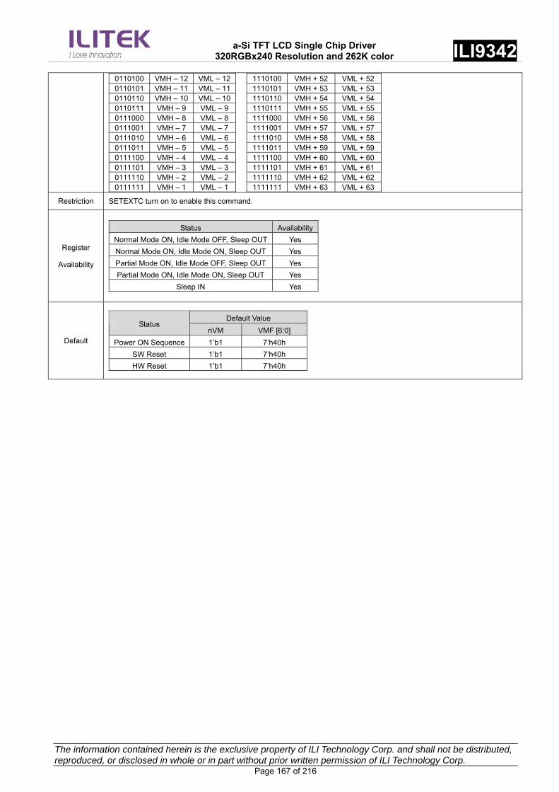
a-Si TFT LCD Single Chip Driver
320RGBx240 Resolution and 262K color ILI9342
The information contained herein is the exclusive property of ILI Technology Corp. and shall not be distributed, reproduced, or disclosed in whole or in part without prior written permission of ILI Technology Corp. Page 167 of 216
0110100 VMH – 12 VML – 12 1110100 VMH + 52 VML + 520110101 VMH – 11 VML – 11 1110101 VMH + 53 VML + 530110110 VMH – 10 VML – 10 1110110 VMH + 54 VML + 540110111 VMH – 9 VML – 9 1110111 VMH + 55 VML + 550111000 VMH – 8 VML – 8 1111000 VMH + 56 VML + 560111001 VMH – 7 VML – 7 1111001 VMH + 57 VML + 570111010 VMH – 6 VML – 6 1111010 VMH + 58 VML + 580111011 VMH – 5 VML – 5 1111011 VMH + 59 VML + 590111100 VMH – 4 VML – 4 1111100 VMH + 60 VML + 600111101 VMH – 3 VML – 3 1111101 VMH + 61 VML + 610111110 VMH – 2 VML – 2 1111110 VMH + 62 VML + 620111111 VMH – 1 VML – 1 1111111 VMH + 63 VML + 63
Restriction SETEXTC turn on to enable this command.
Register
Availability
Status Availability
Normal Mode ON, Idle Mode OFF, Sleep OUT Yes
Normal Mode ON, Idle Mode ON, Sleep OUT Yes
Partial Mode ON, Idle Mode OFF, Sleep OUT Yes
Partial Mode ON, Idle Mode ON, Sleep OUT Yes
Sleep IN Yes
Default
Default Value Status
nVM VMF [6:0]
Power ON Sequence 1’b1 7’h40h
SW Reset 1’b1 7’h40h
HW Reset 1’b1 7’h40h
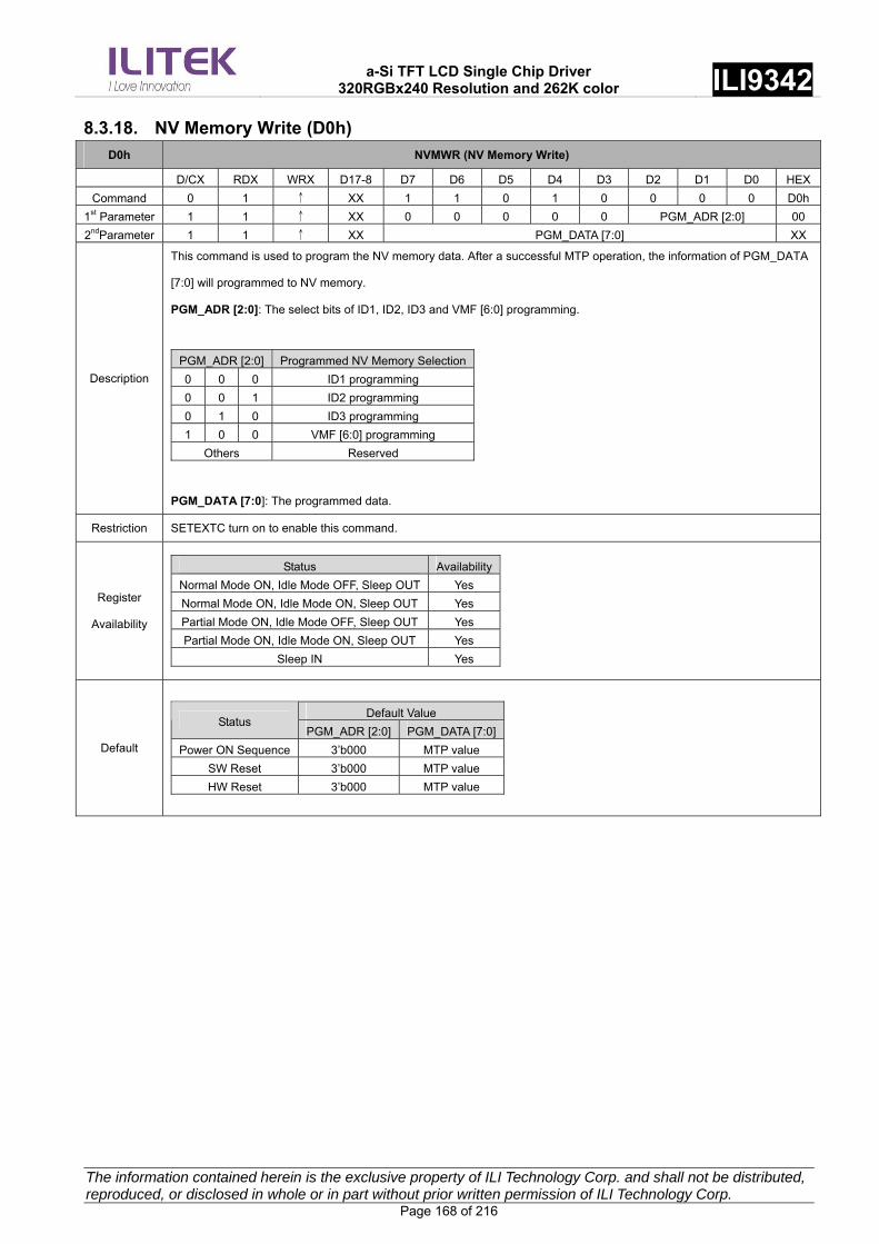
a-Si TFT LCD Single Chip Driver
320RGBx240 Resolution and 262K color ILI9342
The information contained herein is the exclusive property of ILI Technology Corp. and shall not be distributed, reproduced, or disclosed in whole or in part without prior written permission of ILI Technology Corp. Page 168 of 216
8.3.18. NV Memory Write (D0h)
D0h NVMWR (NV Memory Write)
D/CX RDX WRX D17-8 D7 D6 D5 D4 D3 D2 D1 D0 HEX
Command 0 1 ↑ XX 1 1 0 1 0 0 0 0 D0h
1st Parameter 1 1 ↑ XX 0 0 0 0 0 PGM_ADR [2:0] 00
2ndParameter 1 1 ↑ XX PGM_DATA [7:0] XX
Description
This command is used to program the NV memory data. After a successful MTP operation, the information of PGM_DATA
[7:0] will programmed to NV memory.
PGM_ADR [2:0]: The select bits of ID1, ID2, ID3 and VMF [6:0] programming.
PGM_ADR [2:0] Programmed NV Memory Selection
0 0 0 ID1 programming
0 0 1 ID2 programming
0 1 0 ID3 programming
1 0 0 VMF [6:0] programming
Others Reserved
PGM_DATA [7:0]: The programmed data.
Restriction SETEXTC turn on to enable this command.
Register
Availability
Status Availability
Normal Mode ON, Idle Mode OFF, Sleep OUT Yes
Normal Mode ON, Idle Mode ON, Sleep OUT Yes
Partial Mode ON, Idle Mode OFF, Sleep OUT Yes
Partial Mode ON, Idle Mode ON, Sleep OUT Yes
Sleep IN Yes
Default
Default Value Status
PGM_ADR [2:0] PGM_DATA [7:0]
Power ON Sequence 3’b000 MTP value
SW Reset 3’b000 MTP value
HW Reset 3’b000 MTP value

a-Si TFT LCD Single Chip Driver
320RGBx240 Resolution and 262K color ILI9342
The information contained herein is the exclusive property of ILI Technology Corp. and shall not be distributed, reproduced, or disclosed in whole or in part without prior written permission of ILI Technology Corp. Page 169 of 216
8.3.19. NV Memory Protection Key (D1h)
D1h NVMPKEY (NV Memory Protection Key)
D/CX RDX WRX D17-8 D7 D6 D5 D4 D3 D2 D1 D0 HEX
Command 0 1 ↑ XX 1 1 0 1 0 0 0 1 D1h
1stParameter 1 1 ↑ XX KEY [23:16] 55h
2ndParameter 1 1 ↑ XX KEY [15:8] AAh
3rdParameter 1 1 ↑ XX KEY [7:0] 66h
Description
KEY [23:0]: NV memory programming protection key. When writing MTP data to D1h, this register must be set to
0x55AA66h to enable MTP programming. If D1h register is not written with 0x55AA66h, then NV memory programming will
be aborted.
Restriction SETEXTC turn on to enable this command.
Register
Availability
Status Availability
Normal Mode ON, Idle Mode OFF, Sleep OUT Yes
Normal Mode ON, Idle Mode ON, Sleep OUT Yes
Partial Mode ON, Idle Mode OFF, Sleep OUT Yes
Partial Mode ON, Idle Mode ON, Sleep OUT Yes
Sleep IN Yes
Default
Status Default Value
Power ON Sequence KEY [23:0]=55AA66h
SW Reset KEY [23:0]=55AA66h
HW Reset KEY [23:0]=55AA66h
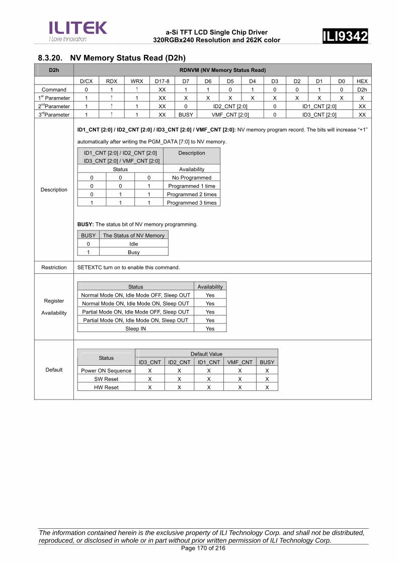
a-Si TFT LCD Single Chip Driver
320RGBx240 Resolution and 262K color ILI9342
The information contained herein is the exclusive property of ILI Technology Corp. and shall not be distributed, reproduced, or disclosed in whole or in part without prior written permission of ILI Technology Corp. Page 170 of 216
8.3.20. NV Memory Status Read (D2h)
D2h RDNVM (NV Memory Status Read)
D/CX RDX WRX D17-8 D7 D6 D5 D4 D3 D2 D1 D0 HEX
Command 0 1 ↑ XX 1 1 0 1 0 0 1 0 D2h
1st Parameter 1 ↑ 1 XX X X X X X X X X X
2ndParameter 1 ↑ 1 XX 0 ID2_CNT [2:0] 0 ID1_CNT [2:0] XX
3rdParameter 1 ↑ 1 XX BUSY VMF_CNT [2:0] 0 ID3_CNT [2:0] XX
Description
ID1_CNT [2:0] / ID2_CNT [2:0] / ID3_CNT [2:0] / VMF_CNT [2:0]: NV memory program record. The bits will increase “+1”
automatically after writing the PGM_DATA [7:0] to NV memory.
ID1_CNT [2:0] / ID2_CNT [2:0]
ID3_CNT [2:0] / VMF_CNT [2:0]
Description
Status Availability
0 0 0 No Programmed
0 0 1 Programmed 1 time
0 1 1 Programmed 2 times
1 1 1 Programmed 3 times
BUSY: The status bit of NV memory programming.
BUSY The Status of NV Memory
0 Idle
1 Busy
Restriction SETEXTC turn on to enable this command.
Register
Availability
Status Availability
Normal Mode ON, Idle Mode OFF, Sleep OUT Yes
Normal Mode ON, Idle Mode ON, Sleep OUT Yes
Partial Mode ON, Idle Mode OFF, Sleep OUT Yes
Partial Mode ON, Idle Mode ON, Sleep OUT Yes
Sleep IN Yes
Default
Default Value Status
ID3_CNT ID2_CNT ID1_CNT VMF_CNT BUSY
Power ON Sequence X X X X X
SW Reset X X X X X
HW Reset X X X X X

a-Si TFT LCD Single Chip Driver
320RGBx240 Resolution and 262K color ILI9342
The information contained herein is the exclusive property of ILI Technology Corp. and shall not be distributed, reproduced, or disclosed in whole or in part without prior written permission of ILI Technology Corp. Page 171 of 216
8.3.21. Read ID4 (D3h)
D3h RDID4 (Read ID4)
D/CX RDX WRX D17-8 D7 D6 D5 D4 D3 D2 D1 D0 HEX
Command 0 1 ↑ XX 1 1 0 1 0 0 1 1 D3h
1st Parameter 1 ↑ 1 XX X X X X X X X X X
2ndParameter 1 ↑ 1 XX 0 0 0 0 0 0 0 0 00h
3rdParameter 1 ↑ 1 XX 1 0 0 1 0 0 1 1 93h
4th Parameter 1 ↑ 1 XX 0 1 0 0 0 0 1 0 42h
Description
Read IC device code.
The 1st parameter is dummy read period.
The 2nd parameter means the IC version.
The 3rd and 4th parameter mean the IC model name.
Restriction SETEXTC turn on to enable this command.
Register
Availability
Status Availability
Normal Mode ON, Idle Mode OFF, Sleep OUT Yes
Normal Mode ON, Idle Mode ON, Sleep OUT Yes
Partial Mode ON, Idle Mode OFF, Sleep OUT Yes
Partial Mode ON, Idle Mode ON, Sleep OUT Yes
Sleep IN Yes
Default
Status Default Value
Power ON Sequence 24’h009342h
SW Reset 24’h009342h
HW Reset 24’h009342h
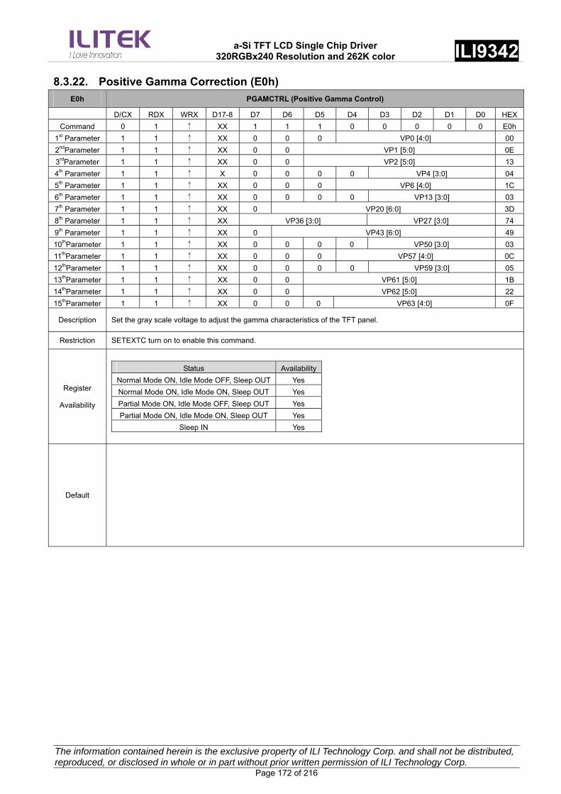
a-Si TFT LCD Single Chip Driver
320RGBx240 Resolution and 262K color ILI9342
The information contained herein is the exclusive property of ILI Technology Corp. and shall not be distributed, reproduced, or disclosed in whole or in part without prior written permission of ILI Technology Corp. Page 172 of 216
8.3.22. Positive Gamma Correction (E0h)
E0h PGAMCTRL (Positive Gamma Control)
D/CX RDX WRX D17-8 D7 D6 D5 D4 D3 D2 D1 D0 HEX
Command 0 1 ↑ XX 1 1 1 0 0 0 0 0 E0h
1st Parameter 1 1 ↑ XX 0 0 0 VP0 [4:0] 00
2ndParameter 1 1 ↑ XX 0 0 VP1 [5:0] 0E
3rdParameter 1 1 ↑ XX 0 0 VP2 [5:0] 13
4th Parameter 1 1 ↑ X 0 0 0 0 VP4 [3:0] 04
5th Parameter 1 1 ↑ XX 0 0 0 VP6 [4:0] 1C
6th Parameter 1 1 ↑ XX 0 0 0 0 VP13 [3:0] 03
7th Parameter 1 1 ↑ XX 0 VP20 [6:0] 3D
8th Parameter 1 1 ↑ XX VP36 [3:0] VP27 [3:0] 74
9th Parameter 1 1 ↑ XX 0 VP43 [6:0] 49
10thParameter 1 1 ↑ XX 0 0 0 0 VP50 [3:0] 03
11thParameter 1 1 ↑ XX 0 0 0 VP57 [4:0] 0C
12thParameter 1 1 ↑ XX 0 0 0 0 VP59 [3:0] 05
13thParameter 1 1 ↑ XX 0 0 VP61 [5:0] 1B
14thParameter 1 1 ↑ XX 0 0 VP62 [5:0] 22
15thParameter 1 1 ↑ XX 0 0 0 VP63 [4:0] 0F
Description Set the gray scale voltage to adjust the gamma characteristics of the TFT panel.
Restriction SETEXTC turn on to enable this command.
Register
Availability
Status Availability
Normal Mode ON, Idle Mode OFF, Sleep OUT Yes
Normal Mode ON, Idle Mode ON, Sleep OUT Yes
Partial Mode ON, Idle Mode OFF, Sleep OUT Yes
Partial Mode ON, Idle Mode ON, Sleep OUT Yes
Sleep IN Yes
Default

a-Si TFT LCD Single Chip Driver
320RGBx240 Resolution and 262K color ILI9342
The information contained herein is the exclusive property of ILI Technology Corp. and shall not be distributed, reproduced, or disclosed in whole or in part without prior written permission of ILI Technology Corp. Page 173 of 216
8.3.23. Negative Gamma Correction (E1h)
E1h NGAMCTRL (Negative Gamma Correction)
D/CX RDX WRX D17-8 D7 D6 D5 D4 D3 D2 D1 D0 HEX
Command 0 1 ↑ XX 1 1 1 0 0 0 0 1 E1h
1st Parameter 1 1 ↑ XX 0 0 0 VN0 [4:0] 00
2ndParameter 1 1 ↑ XX 0 0 VN1 [5:0] 23
3rdParameter 1 1 ↑ XX 0 0 VN2 [5:0] 26
4th Parameter 1 1 ↑ XX 0 0 0 0 VN4 [3:0] 05
5th Parameter 1 1 ↑ XX 0 0 0 VN6 [4:0] 10
6th Parameter 1 1 ↑ XX 0 0 0 0 VN13 [3:0] 04
7th Parameter 1 1 ↑ XX 0 VN20 [6:0] 39
8th Parameter 1 1 ↑ XX VN36 [3:0] VN27 [3:0] 24
9th Parameter 1 1 ↑ XX 0 VN43 [6:0] 4B
10thParameter 1 1 ↑ XX 0 0 0 0 VN50 [3:0] 03
11thParameter 1 1 ↑ XX 0 0 0 VN57 [4:0] 0B
12thParameter 1 1 ↑ XX 0 0 0 0 VN59 [3:0] 0B
13thParameter 1 1 ↑ XX 0 0 VN61 [5:0] 33
14thParameter 1 1 ↑ XX 0 0 VN62 [5:0] 37
15thParameter 1 1 ↑ XX 0 0 0 VN63 [4:0] 0F
Description Set the gray scale voltage to adjust the gamma characteristics of the TFT panel.
Restriction SETEXTC turn on to enable this command.
Register
Availability
Status Availability
Normal Mode ON, Idle Mode OFF, Sleep OUT Yes
Normal Mode ON, Idle Mode ON, Sleep OUT Yes
Partial Mode ON, Idle Mode OFF, Sleep OUT Yes
Partial Mode ON, Idle Mode ON, Sleep OUT Yes
Sleep IN Yes
Default
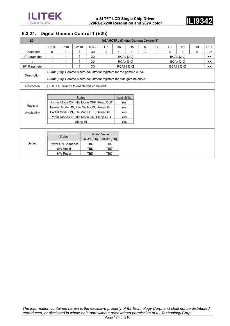
a-Si TFT LCD Single Chip Driver
320RGBx240 Resolution and 262K color ILI9342
The information contained herein is the exclusive property of ILI Technology Corp. and shall not be distributed, reproduced, or disclosed in whole or in part without prior written permission of ILI Technology Corp. Page 174 of 216
8.3.24. Digital Gamma Control 1 (E2h)
E2h DGAMCTRL (Digital Gamma Control 1)
D/CX RDX WRX D17-8 D7 D6 D5 D4 D3 D2 D1 D0 HEX
Command 0 1 ↑ XX 1 1 1 0 0 0 1 0 E2h
1st Parameter 1 1 ↑ XX RCA0 [3:0] BCA0 [3:0] XX
: 1 1 ↑ XX RCAx [3:0] BCAx [3:0] XX
16th Parameter 1 1 ↑ XX RCA15 [3:0] BCA15 [3:0] XX
Description RCAx [3:0]: Gamma Macro-adjustment registers for red gamma curve.
BCAx [3:0]: Gamma Macro-adjustment registers for blue gamma curve.
Restriction SETEXTC turn on to enable this command.
Register
Availability
Status Availability
Normal Mode ON, Idle Mode OFF, Sleep OUT Yes
Normal Mode ON, Idle Mode ON, Sleep OUT Yes
Partial Mode ON, Idle Mode OFF, Sleep OUT Yes
Partial Mode ON, Idle Mode ON, Sleep OUT Yes
Sleep IN Yes
Default
Default Value Status
RCAx [3:0] BCAx [3:0]
Power ON Sequence TBD TBD
SW Reset TBD TBD
HW Reset TBD TBD
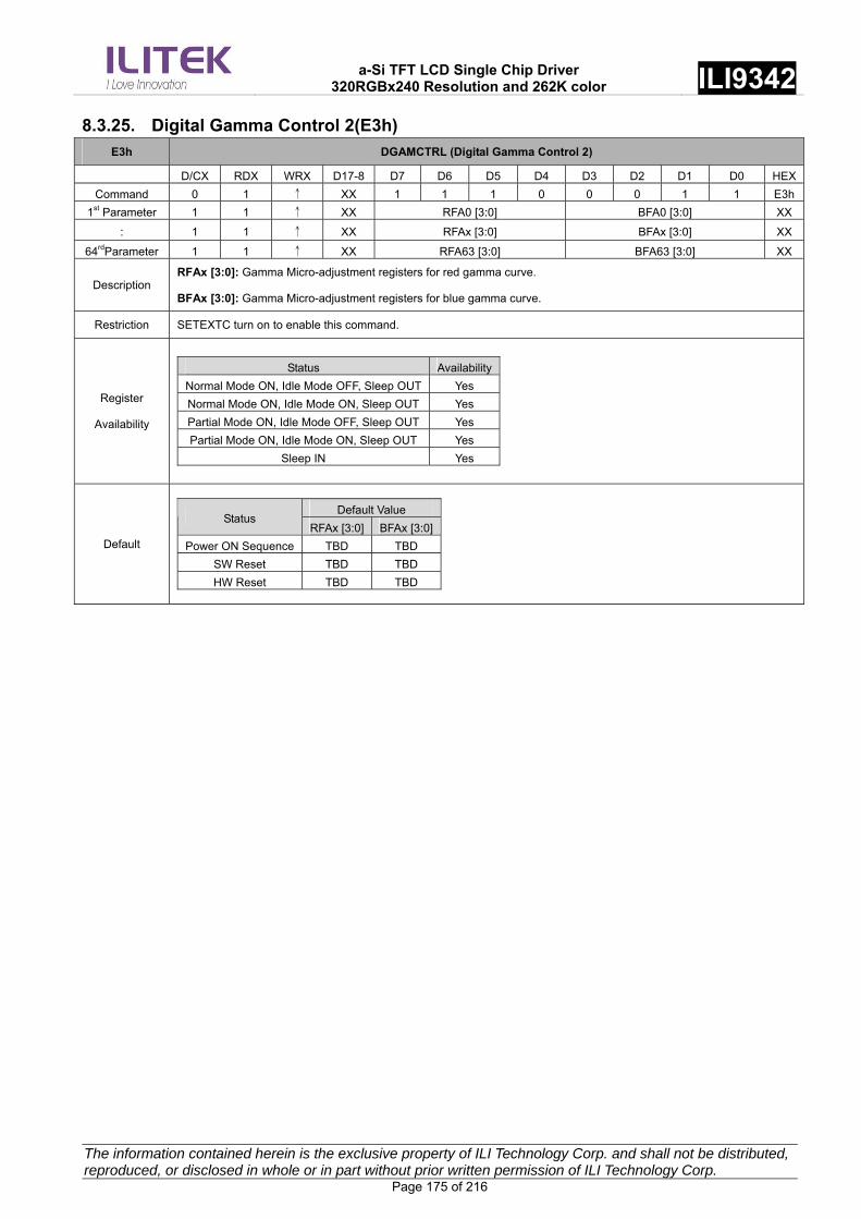
a-Si TFT LCD Single Chip Driver
320RGBx240 Resolution and 262K color ILI9342
The information contained herein is the exclusive property of ILI Technology Corp. and shall not be distributed, reproduced, or disclosed in whole or in part without prior written permission of ILI Technology Corp. Page 175 of 216
8.3.25. Digital Gamma Control 2(E3h)
E3h DGAMCTRL (Digital Gamma Control 2)
D/CX RDX WRX D17-8 D7 D6 D5 D4 D3 D2 D1 D0 HEX
Command 0 1 ↑ XX 1 1 1 0 0 0 1 1 E3h
1st Parameter 1 1 ↑ XX RFA0 [3:0] BFA0 [3:0] XX
: 1 1 ↑ XX RFAx [3:0] BFAx [3:0] XX
64rdParameter 1 1 ↑ XX RFA63 [3:0] BFA63 [3:0] XX
Description RFAx [3:0]: Gamma Micro-adjustment registers for red gamma curve.
BFAx [3:0]: Gamma Micro-adjustment registers for blue gamma curve.
Restriction SETEXTC turn on to enable this command.
Register
Availability
Status Availability
Normal Mode ON, Idle Mode OFF, Sleep OUT Yes
Normal Mode ON, Idle Mode ON, Sleep OUT Yes
Partial Mode ON, Idle Mode OFF, Sleep OUT Yes
Partial Mode ON, Idle Mode ON, Sleep OUT Yes
Sleep IN Yes
Default
Default Value Status
RFAx [3:0] BFAx [3:0]
Power ON Sequence TBD TBD
SW Reset TBD TBD
HW Reset TBD TBD

a-Si TFT LCD Single Chip Driver
320RGBx240 Resolution and 262K color ILI9342
The information contained herein is the exclusive property of ILI Technology Corp. and shall not be distributed, reproduced, or disclosed in whole or in part without prior written permission of ILI Technology Corp. Page 176 of 216
8.3.26. Interface Control (F6h)
F6h IFCTL (16bits Data Format Selection)
D/CX RDX WRX D17-8 D7 D6 D5 D4 D3 D2 D1 D0 HEX
Command 0 1 ↑ XX 1 1 1 1 0 1 1 0 F6h
1stParameter 1 1 ↑ XX MY_
EOR
MX_
EOR
MV_
EOR0
BGR_
EOR0 0
WE
MODE01
2ndParameter 1 1 ↑ XX 0 0 EPF [1:0] 0 0 0 0 00
3rdParameter 1 1 ↑ XX 0 0 ENDIAN 0 DM [1:0] RM RIM 00
Description
MY_EOR / MX_EOR / MV_EOR / BGR_EOR:
The set value of MADCTL is used in the IC is derived as exclusive OR between 1st Parameter of IFCTL and MADCTL
Parameter.
WEMODE: Memory write control
WEMODE=0: When the transfer number of data exceeds (EC-SC+1)*(EP-SP+1), the exceeding data will be ignored.
WEMODE=1: When the transfer number of data exceeds (EC-SC+1)*(EP-SP+1), the column and page number will be
reset, and the exceeding data will be written into the following column and page.
ENDIAN: Select Little Endian Interface bit. At Little Endian mode, the host sends LSB data first.
ENDIAN Data transfer Mode
0 Normal (MSB first, default)
1 Little Endian (LSB first)
DB[7] DB[6] DB [5] DB[4] DB[3] DB[2] DB[1] DB [0] DB[7] DB[6] DB [5] DB[4] DB[3] DB [2] DB[1] DB[0]
R4 R3 R2 R1 R0 G5 G4 G3 G2 G1 G0 B 4 B3 B2 B1 B0
1st transfer ( Lower byte) 2nd transfer (Upper byte)
DB[7] DB[6] DB [5] DB[4] DB[3] DB[2] DB [1] DB[0] DB [7] DB[6] DB[5] DB[4] DB[3] DB[2] DB[1 ] DB [0]
Input Data
16-b it display Data(Before expanding to
18 bi ts data)
Note: Little Endian is valid on only 65K 8-bit and 9-bit MPU interface mode.
DM [1:0]: Select the display operation mode.
DM [1] DM [0] Display Operation Mode
0 0 Internal clock operation
0 1 RGB Interface Mode
1 0 VSYNC interface mode
1 1 Setting disabled
The DM [1:0] setting allows switching between internal clock operation mode and external display interface operation mode.
However, switching between the RGB interface operation mode and the VSYNC interface operation mode is prohibited.
RM: Select the interface to access the GRAM.
Set RM to “1” when writing display data by the RGB interface.
RM Interface for RAM Access
0 System interface/VSYNC interface
1 RGB interface

a-Si TFT LCD Single Chip Driver
320RGBx240 Resolution and 262K color ILI9342
The information contained herein is the exclusive property of ILI Technology Corp. and shall not be distributed, reproduced, or disclosed in whole or in part without prior written permission of ILI Technology Corp. Page 177 of 216
RIM: Specify the RGB interface mode when the RGB interface is used. These bits should be set before display operation
through the RGB interface and should not be set during operation.
RIM COLMOD [6:4] RGB Interface Mode
110 (262K color) 18- bit RGB interface (1 transfer/pixel) 0
101 (65K color) 16- bit RGB interface (1 transfer/pixel)
110 (262K color) 6- bit RGB interface (3 transfer/pixel) 1
101 (65K color) 6- bit RGB interface (3 transfer/pixel)
EPF [1:0]: 65K color mode data format.
R5 R4 R3 R2 R1 G5 G4 G3 G2 G1 G0 B4 B3 B2 B1 00 B5
Data Bus
Frame Data
Read Data
EPF=00
R5 R4 R3 R2 R1 G5 G4 G3 G2 G1 G0 B4 B3 B2 B1 11 B5
Data Bus
Frame Data
Read Data
EPF=01
DB17 DB16 DB15 DB14 DB13 DB12 DB11 DB10 DB8 DB7 DB6 DB5 DB4 DB3 DB2 DB1
R5 R4 R3 R2 R1 G5 G4 G3 G2 G1 G0 B4 B3 B2 B1 B0R0 B5
Data Bus
Frame Data
Read Data
EPF=10
R5 R4 R3 R2 R1 G5 G4 G3 G2 G1 G0 B4 B3 B2 B1 B0R0 B5
Data Bus
Frame Data
Read Data
EPF=11 Condition CopyCondition Copy
DB17 DB16 DB15 DB14 DB13 DB12 DB11 DB10 DB8 DB7 DB6 DB5 DB4 DB3 DB2 DB1
DB17 DB16 DB15 DB14 DB13 DB12 DB11 DB10 DB8 DB7 DB6 DB5 DB4 DB3 DB2 DB1
DB17 DB16 DB15 DB14 DB13 DB12 DB11 DB10 DB8 DB7 DB6 DB5 DB4 DB3 DB2 DB1
DB17 DB16 DB15 DB14 DB13 DB12 DB11 DB10 DB8 DB7 DB6 DB5 DB4 DB3 DB2 DB1
DB17 DB16 DB15 DB14 DB13 DB12 DB11 DB10 DB8 DB7 DB6 DB5 DB4 DB3 DB2 DB1
DB17 DB16 DB15 DB14 DB13 DB12 DB11 DB10 DB8 DB7 DB6 DB5 DB4 DB3 DB2 DB1
DB17 DB16 DB15 DB14 DB13 DB12 DB11 DB10 DB8 DB7 DB6 DB5 DB4 DB3 DB2 DB1

a-Si TFT LCD Single Chip Driver
320RGBx240 Resolution and 262K color ILI9342
The information contained herein is the exclusive property of ILI Technology Corp. and shall not be distributed, reproduced, or disclosed in whole or in part without prior written permission of ILI Technology Corp. Page 178 of 216
Green Data
Input data
R/B Data
Green data = odd
Green data = even
By-pass G0 is copied to
R0/B0
R=B
R != B
EPF [1:0] Expand 16 bbp (R,G,B) to 18bbp (R,G,B)
00
MSB is inputted to LSB r [5:0] = {R [4:0], R [4]} g [5:0] = {G [5:0]} b [5:0] = {B [4:0], B [4]}
01
“0” is inputted to LSB r [5:0] = {R [4:0], 0} g [5:0] = {G [5:0]} b [5:0] = {B [4:0], 0} Exception: R [4:0], B[4:0] = 5’h1F → r [5:0], b[5:0] = 6’h3F
10
“1” is inputted to LSB r [5:0] = {R [4:0], 1} g [5:0] = {G [5:0]} b [5:0] = {B [4:0], 1} Exception: R [4:0], B[4:0] = 5’h00 → r [5:0], b[5:0] = 6’h00
11
Compare R [4:0], G [5:1], B [4:0] case: Case 1: R=G=B → r [5:0] = {R [4:0], G [0]}, g [5:0] = {G [5:0]}, b [5:0] = {B [4:0], G [0]} Case 2: R=B≠G → r [5:0] = {R [4:0], R [4]}, g [5:0] = {G [5:0]}, b [5:0] = {B [4:0], B [0]} Case 3: R=G≠B → r [5:0] = {R [4:0], G [0]}, g [5:0] = {G [5:0]}, b [5:0] = {B [4:0], B [0]} Case 4: B=G≠R → r [5:0] = {R [4:0], R [4]}, g [5:0] = {G [5:0]}, b [5:0] = {B [4:0], G [0]}
Restriction SETEXTC turn on to enable this command.
Register
Availability
Status Availability
Normal Mode ON, Idle Mode OFF, Sleep OUT Yes
Normal Mode ON, Idle Mode ON, Sleep OUT Yes
Partial Mode ON, Idle Mode OFF, Sleep OUT Yes
Partial Mode ON, Idle Mode ON, Sleep OUT Yes
Sleep IN Yes
Default
Default Value Status
EPF [1:0] ENDIAN WEMODE DM [1:0] RM RIM
Power ON Sequence 2’b00 1’b0 1’b1 2’b00 1’b0 1’b0
SW Reset 2’b00 1’b0 1’b1 2’b00 1’b0 1’b0
HW Reset 2’b00 1’b0 1’b1 2’b00 1’b0 1’b0

a-Si TFT LCD Single Chip Driver
320RGBx240 Resolution and 262K color ILI9342
The information contained herein is the exclusive property of ILI Technology Corp. and shall not be distributed, reproduced, or disclosed in whole or in part without prior written permission of ILI Technology Corp. Page 179 of 216
8.3.27. Get GPIO0~7 Status (F7h)
F7h Get GPIO0~7 Status
D/CX RDX WRX D17-8 D7 D6 D5 D4 D3 D2 D1 D0 HEX
Command 0 1 ↑ XX 1 1 1 1 0 1 1 1 F7h
1st Parameter 1 ↑ 1 XX X X X X X X X X X
2ndParameter 1 ↑ 1 XX GPI[7:0] 00
Description
GPI[7:0]: get the GPIO0~7 input configuration correspondent with register GPI bit 0 ~ 7.
0 : logic low input
1 : logic High input
Restriction SETEXTC turn on to enable this command.
Register
Availability
Status Availability
Normal Mode ON, Idle Mode OFF, Sleep OUT Yes
Normal Mode ON, Idle Mode ON, Sleep OUT Yes
Partial Mode ON, Idle Mode OFF, Sleep OUT Yes
Partial Mode ON, Idle Mode ON, Sleep OUT Yes
Sleep IN Yes
Default
Default Value Status
GPI[7:0]
Power ON Sequence 7’h00h
SW Reset 7’h00h
HW Reset 7’h00h

a-Si TFT LCD Single Chip Driver
320RGBx240 Resolution and 262K color ILI9342
The information contained herein is the exclusive property of ILI Technology Corp. and shall not be distributed, reproduced, or disclosed in whole or in part without prior written permission of ILI Technology Corp. Page 180 of 216
8.3.28. Set GPIO0~7 Status (F8h)
F8h Set GPIO0~7 Status
D/CX RDX WRX D17-8 D7 D6 D5 D4 D3 D2 D1 D0 HEX
Command 0 1 ↑ XX 1 1 1 1 1 0 0 0 F8h
1st Parameter 1 1 ↑ XX GPO[7:0] 00
2ndParameter 1 1 ↑ XX IE OEB 00
Description
GPO[7:0] : Setting the GPIO output configuration
0 : GPIO output is logic low
1 : GPIO output is logic High
IE/OEB : Control the GPO output direction
IE OEB GPO output control
0 0 Enable GPIO output
1 1 Disable GPIO output
Restriction SETEXTC turn on to enable this command.
Register
Availability
Status Availability
Normal Mode ON, Idle Mode OFF, Sleep OUT Yes
Normal Mode ON, Idle Mode ON, Sleep OUT Yes
Partial Mode ON, Idle Mode OFF, Sleep OUT Yes
Partial Mode ON, Idle Mode ON, Sleep OUT Yes
Sleep IN Yes
Default
Default Value Status
GPO[7:0] IE OEB
Power ON Sequence 7’h00h 1’b0 1’b0
SW Reset 7’h00h 1’b0 1’b0
HW Reset 7’h00h 1’b0 1’b0

a-Si TFT LCD Single Chip Driver
320RGBx240 Resolution and 262K color ILI9342
The information contained herein is the exclusive property of ILI Technology Corp. and shall not be distributed, reproduced, or disclosed in whole or in part without prior written permission of ILI Technology Corp. Page 181 of 216
9. Display Data RAM
9.1. Configuration The display data RAM stores display dots and consists of 1,382,400 bits (320x18x240 bits). There is no
restriction on access to the RAM even when the display data on the same address is loaded to DAC. There will
be no abnormal visible effect on the display when there is a simultaneous panel read and interface read or write
display data to the same location of the frame memory.
320 x 240 x 18 bitsFrame Memory
Column Counter
Page
Co
unter
MCU Interface
Line Latch (320 ch)
Color Inversion
DAC (320ch)
Amp (320 ch)
Line P
oin
ter
Panel Side
Interface Side
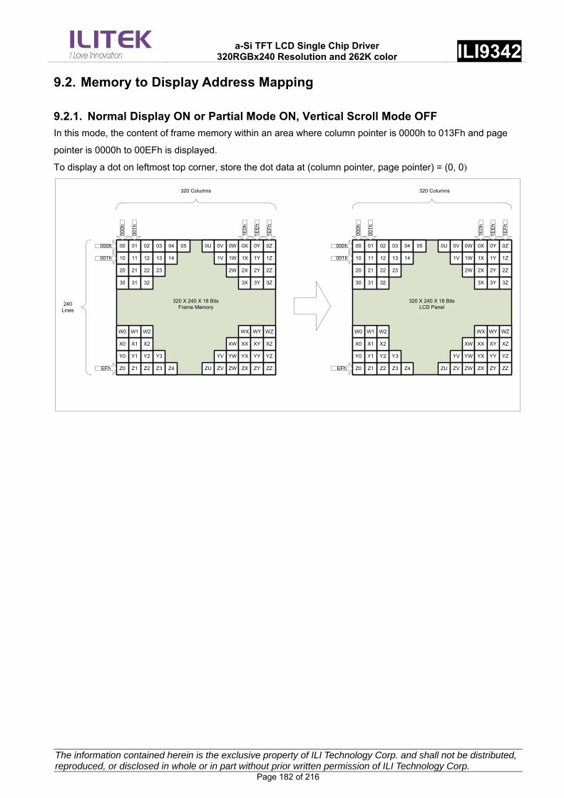
a-Si TFT LCD Single Chip Driver
320RGBx240 Resolution and 262K color ILI9342
The information contained herein is the exclusive property of ILI Technology Corp. and shall not be distributed, reproduced, or disclosed in whole or in part without prior written permission of ILI Technology Corp. Page 182 of 216
9.2. Memory to Display Address Mapping
9.2.1. Normal Display ON or Partial Mode ON, Vertical Scroll Mode OFF
In this mode, the content of frame memory within an area where column pointer is 0000h to 013Fh and page
pointer is 0000h to 00EFh is displayed.
To display a dot on leftmost top corner, store the dot data at (column pointer, page pointer) = (0, 0)
0Z0Y0X0W0V0U
1Z1Y1X1W1V
2Z2Y2X2W
3Z3Y3X
WZWYWX
XZXYXXXW
YYYXYWYV
ZZZYZXZWZVZU
YZ
Z0 Z1 Z2 Z3 Z4
Y0 Y1 Y2 Y3
X0 X1 X2
W0 W1 W2
320 X 240 X 18 BitsFrame Memory
050403020100
1413121110
23222120
323130
000h
001h
1E
Fh
1EE
h
000h
001h
EFh
240 Lines
320 Columns
0Z0Y0X0W0V0U
1Z1Y1X1W1V
2Z2Y2X2W
3Z3Y3X
WZWYWX
XZXYXXXW
YYYXYWYV
ZZZYZXZWZVZU
YZ
Z0 Z1 Z2 Z3 Z4
Y0 Y1 Y2 Y3
X0 X1 X2
W0 W1 W2
320 X 240 X 18 BitsLCD Panel
050403020100
1413121110
23222120
323130
000h
001h
1E
Fh
1EE
h
1ED
h
000h
001h
EFh
320 Columns
1ED
h

a-Si TFT LCD Single Chip Driver
320RGBx240 Resolution and 262K color ILI9342
The information contained herein is the exclusive property of ILI Technology Corp. and shall not be distributed, reproduced, or disclosed in whole or in part without prior written permission of ILI Technology Corp. Page 183 of 216
9.2.2. Vertical Scroll Mode
There is a vertical scrolling mode, which is determined by the commands “Vertical Scrolling Definition” (33h) and
“Vertical Scrolling Start Address” (37h).
The Vertical Scroll Mode function is explained by these examples in the following.
0Z0Y0X0W0V0U
1Z1Y1X1W1V
2Z2Y2X2W
3Z3Y3X
WZWYWX
XZXYXXXW
YYYXYWYV
ZZZYZXZWZVZU
YZ
Z0 Z1 Z2 Z3 Z4
Y0 Y1 Y2 Y3
X0 X1 X2
W0 W1 W2
320 X 240 X 18 BitsFrame Memory
050403020100
1413121110
23222120
323130
000h
001h
1E
Fh
1E
Eh
1E
Dh
000h
001h
EFh
0Z0Y0X0W0V0U
1Z1Y1X1W1V
3Z3Y3X3W
4Z4Y4X
XZ
XYXX
YYYXYW
ZZZYZXZWZV
YZ
Z0 Z1 Z2 Z3
Y0 Y1 Y2
X0 X1 X2
320 X 240 X 18 BitsLCD Panel
050403020100
1413121110
33323130
424140
000h
001h
1E
Fh
1E
Eh
1E
Dh
000h
001h
EFh
EEh
EDh
Scroll Pointer = 03h
EEh
EDh
XZ
2Z2Y2X2W2V2U20 21 22 23 24
TFA=2, VSA=238, BFA=0 when MADCTL MV bit = 0
Scroll area
= 238lines
0Z0Y0X0W0V0U
1Z1Y1X1W1V
2Z2Y2X2W
3Z3Y3X
WZWYWX
XZXYXXXW
YYYXYWYV
ZZZYZXZWZVZU
YZ
Z0 Z1 Z2 Z3 Z4
Y0 Y1 Y2 Y3
X0 X1 X2
W0 W1 W2
320 X 240 X 18 BitsFrame Memory
050403020100
1413121110
23222120
323130
000h
001h
1E
Fh
1EE
h
1E
Dh
000h
001h
EFh
0Z0Y0X0W0V0U
1Z1Y1X1W1V
3Z3Y3X3W
4Z4Y4X
XYXXX0 X1 X2
320 X 240 X 18 BitsLCD Panel
050403020100
1413121110
33323130
424140
000h
001h
1E
Fh
1EE
h
1E
Dh
000h
001h
EFh
EEh
EDh
Scroll Pointer = 03h
EEh
EDh
XZ
2Z2Y2X2W20 21 22 23
TFA=2, VSA=236, BFA=2 when MADCTL MV bit = 0
YYYXYWYV
ZZZYZXZWZVZU
YZ
Z0 Z1 Z2 Z3 Z4
Y0 Y1 Y2 Y3
Top fixed area
Scroll area
Bottom fixed area
Scroll area
= 236lines
0Z0Y0X0W0V0U
1Z1Y1X1W1V
2Z2Y2X2W
3Z3Y3X
WZWYWX
XZXYXXXW
YYYXYWYV
ZZZYZXZWZVZU
YZ
Z0 Z1 Z2 Z3 Z4
Y0 Y1 Y2 Y3
X0 X1 X2
W0 W1 W2
320 X 240 X 18 BitsFrame Memory
050403020100
1413121110
23222120
323130
000h
001h
1E
Fh
1E
Eh
1ED
h
000h
001h
EFh
0Z0Y0X0W0V0U
1Z1Y1X1W1V
3Z3Y3X3W
4Z4Y4X
3Y3X30 31 32
320 X 240 X 18 BitsLCD Panel
050403020100
1413121110
33323130
424140
000h
001h
1E
Fh
1E
Eh
1ED
h
000h
001h
EFh
EEh
EDh
Scroll Pointer = 05h
EEh
EDh
3Z
4Z4Y4X4W40 41 42 43
TFA=0, VSA=236, BFA=4 when MADCTL MV bit = 0
YYYXYWYV
ZZZYZXZWZVZU
YZ
Z0 Z1 Z2 Z3 Z4
Y0 Y1 Y2 Y3
Top fixed area
Scroll area
Bottom fixed area
Scroll area
= 236lines
Note: When Vertical Scrolling Definition Parameters (TFA+VSA+BFA) ≠ 240, Scrolling Mode is undefined.

a-Si TFT LCD Single Chip Driver
320RGBx240 Resolution and 262K color ILI9342
The information contained herein is the exclusive property of ILI Technology Corp. and shall not be distributed, reproduced, or disclosed in whole or in part without prior written permission of ILI Technology Corp. Page 184 of 216
9.2.3. Vertical Scroll Example
9.2.4. Case1: TFA+VSA+BFA < 240
This setting is prohibited, unless unexpected picture will be shown.
9.2.5. Case2: TFA+VSA+BFA = 240 (Rolling Scrolling)
The operation of Rolling Scrolling is explained by these examples in the following.
Memory Physical
Axis (0,0)
VSCRSADD
Display Axis (0,0)
12
12
When TFA=0, VSA=240, BFA=0, VSCRSADD=40 and MADCTL MV bit = 1
Physical Line PointerMemory Physical
Axis (0,0)
VSCRSADD
Display Axis (0,0)
12
When TFA=0, VSA=240, BFA=0, VSCRSADD=40 and MADCTL MV bit = 0
Physical Line PointerMemory Physical
Axis (0,0)
VSCRSADD
Display Axis (0,0)
12
12
21
Increment VSCRSADD

a-Si TFT LCD Single Chip Driver
320RGBx240 Resolution and 262K color ILI9342
The information contained herein is the exclusive property of ILI Technology Corp. and shall not be distributed, reproduced, or disclosed in whole or in part without prior written permission of ILI Technology Corp. Page 185 of 216
Memory Physical
Axis (0,0)
VSCRSADD
Display Axis (0,0)
23
When TFA=30, VSA=210, BFA=0, VSCRSADD=80 and MADCTL MV bit = 0
1
TFA 23
1
TFA
Physical Line PointerMemory Physical
Axis (0,0)
VSCRSADD
Display Axis (0,0)
When TFA=30, VSA=210, BFA=0, VSCRSADD=80 and MADCTL MV bit = 1
Physical Line PointerMemory Physical
Axis (0,0)
VSCRSADD
Display Axis (0,0)
Increment VSCRSADD
TFA
23
1
23
1 TFA
23
TFA
23
1 1
TFA
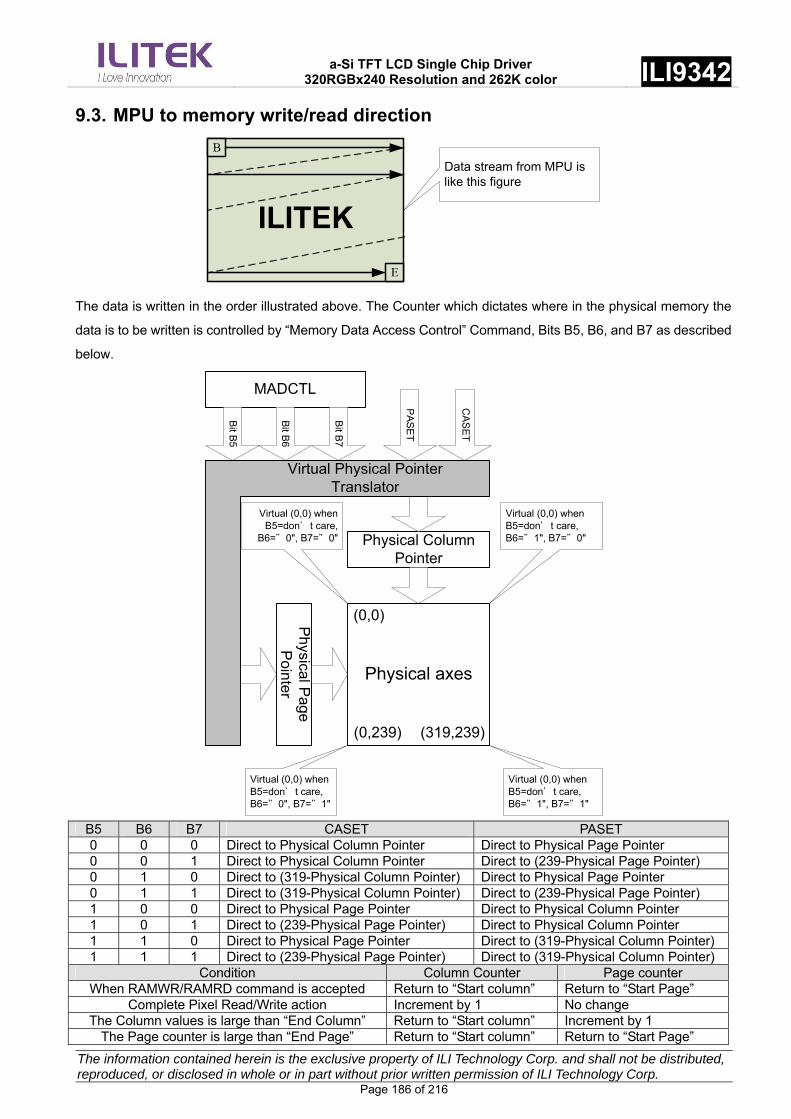
a-Si TFT LCD Single Chip Driver
320RGBx240 Resolution and 262K color ILI9342
The information contained herein is the exclusive property of ILI Technology Corp. and shall not be distributed, reproduced, or disclosed in whole or in part without prior written permission of ILI Technology Corp. Page 186 of 216
9.3. MPU to memory write/read direction
B
E
ILITEK
Data stream from MPU is like this figure
The data is written in the order illustrated above. The Counter which dictates where in the physical memory the
data is to be written is controlled by “Memory Data Access Control” Command, Bits B5, B6, and B7 as described
below.
Physical axes
(0,0)
(0,239) (319,239)
Physical Column Pointer
Physical P
age P
ointer
MADCTL
Virtual (0,0) when B5=don't care, B6="1", B7="0"
Virtual (0,0) when B5=don't care, B6="1", B7="1"
Bit B
7
Bit B
6
Bit B
5
PA
SE
T
CA
SE
T
Virtual (0,0) when B5=don't care, B6="0", B7="1"
Virtual (0,0) when B5=don't care,
B6="0", B7="0"
Virtual Physical Pointer Translator
B5 B6 B7 CASET PASET 0 0 0 Direct to Physical Column Pointer Direct to Physical Page Pointer 0 0 1 Direct to Physical Column Pointer Direct to (239-Physical Page Pointer) 0 1 0 Direct to (319-Physical Column Pointer) Direct to Physical Page Pointer 0 1 1 Direct to (319-Physical Column Pointer) Direct to (239-Physical Page Pointer) 1 0 0 Direct to Physical Page Pointer Direct to Physical Column Pointer 1 0 1 Direct to (239-Physical Page Pointer) Direct to Physical Column Pointer 1 1 0 Direct to Physical Page Pointer Direct to (319-Physical Column Pointer) 1 1 1 Direct to (239-Physical Page Pointer) Direct to (319-Physical Column Pointer)
Condition Column Counter Page counter When RAMWR/RAMRD command is accepted Return to “Start column” Return to “Start Page”
Complete Pixel Read/Write action Increment by 1 No change The Column values is large than “End Column” Return to “Start column” Increment by 1
The Page counter is large than “End Page” Return to “Start column” Return to “Start Page”

a-Si TFT LCD Single Chip Driver
320RGBx240 Resolution and 262K color ILI9342
The information contained herein is the exclusive property of ILI Technology Corp. and shall not be distributed, reproduced, or disclosed in whole or in part without prior written permission of ILI Technology Corp. Page 187 of 216
Note:
Data is always written to the Frame Memory in the same order, regardless of the Memory Write Direction set by
MADCTL bits B7, B6 and B5. The write order for each pixel unit is
D17R5
D16R4
D15R3
D14R2
D13R1
D12R0
D11G5
D10G4
D9G3
D8G2
D7G1
D6G0
D5B5
D4B4
D3B3
D2B2
D1B1
D0B0
One pixel unit represents 1 column and 1 page counter value on the Frame Memory.

a-Si TFT LCD Single Chip Driver
320RGBx240 Resolution and 262K color ILI9342
The information contained herein is the exclusive property of ILI Technology Corp. and shall not be distributed, reproduced, or disclosed in whole or in part without prior written permission of ILI Technology Corp. Page 188 of 216
MV MX MY
Image in the Memory(MPU)
B
E
000
B
E
100
010
110
Display Data Direction
Normal
MADCTR Parameter Image in the Driver (Frame Memory)
B
E
Memory(0,0)
Counter(0,0)
Y-Mirror
B
E
Memory(0,0)
Counter(0,0)
X-Mirror
B
E
B
E
Memory(0,0) Counter(0,0)
X-MirrorY-Mirror
B
E B
EMemory(0,0)
Counter(0,0)
X-Y Exchange 001
101
011
111
B
E
B
E
Counter(0,0)
X-Y ExchangeY-Mirror
XY ExchangeX-Mirror
XY ExchangeX-MirrorY-Mirror
c
B
E
B
E
B
E
B
E
B
E
B
E
Memor(0,0)
Memory(0,0)
Memory(0,0)
Memory(0,0)
Counter(0,0)
Counter(0,0)
Counter(0,0)

a-Si TFT LCD Single Chip Driver
320RGBx240 Resolution and 262K color ILI9342
The information contained herein is the exclusive property of ILI Technology Corp. and shall not be distributed, reproduced, or disclosed in whole or in part without prior written permission of ILI Technology Corp. Page 189 of 216
10. Tearing Effect Output
The Tearing Effect output line supplies to the MPU a Panel synchronization signal. This signal can be enabled or
disabled by the Tearing Effect Line Off & On commands. The mode of the Tearing Effect Signal is defined by the
parameter of the Tearing Effect Line Off & On commands.
The signal can be used by the MPU to synchronize Frame Memory Writing when displaying video images.
10.1. Tearing Effect Line Modes Mode 1, the Tearing Effect Output signal consists of V-Sync information only:
tvdl tvdh
Vertical Time Scale
tvdh = The LCD display is not updated from the Frame Memory.
tvdl = The LCD display is updated from the Frame Memory (except Invisible Line – see below).
Mode 2, the tearing effect output signal consists of V-Sync and H-Sync information; there is one V-sync and 240
H-sync pulses per field:
tvdl
V-Sync
tvdh
1st Line 240th
Line
V-SyncInvisible
Line
thdh = The LCD display is not updated from the Frame Memory.
thdl = The LCD display is updated from the Frame Memory (except Invisible Line – see above).
Bottom Line
2nd Line
1st Line
TE (mode 2)
TE (mode 1)
Note: During Sleep In Mode, the Tearing Effect Output Pin is active Low.

a-Si TFT LCD Single Chip Driver
320RGBx240 Resolution and 262K color ILI9342
The information contained herein is the exclusive property of ILI Technology Corp. and shall not be distributed, reproduced, or disclosed in whole or in part without prior written permission of ILI Technology Corp. Page 190 of 216
10.2. Tearing Effect Line Timings The tearing effect signal is described below:
tvdh
Vertical Timing
Horizontal Timing
thdl thdh
tvd l
AC characteristics of Tearing Effect Signal (Frame Rate = 60Hz)
Symbol Parameter Min. Typ. Max. Unit Description
tvdl Vertical timing low duration -- -- -- ms
tvdh Vertical timing high duration 1000 -- -- us
thdl Horizontal timing low duration -- -- -- us
thdh Horizontal timing high duration -- -- 500 us
Note:
1. The timings in Table as above apply when MADCTL B4=0 and B4=1
2. The signal’s rise and fall times (tf, tr) are stipulated to be equal to or less than 15ns.
tr tf
80%
20%
80%
20%
The Tearing Effect Output Line is fed back to the MPU and should be used to avoid Tearing Effect.
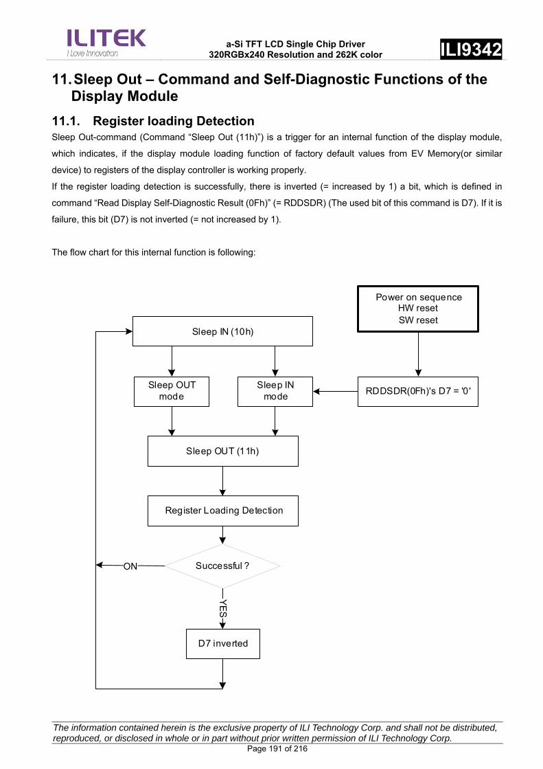
a-Si TFT LCD Single Chip Driver
320RGBx240 Resolution and 262K color ILI9342
The information contained herein is the exclusive property of ILI Technology Corp. and shall not be distributed, reproduced, or disclosed in whole or in part without prior written permission of ILI Technology Corp. Page 191 of 216
11. Sleep Out – Command and Self-Diagnostic Functions of the Display Module
11.1. Register loading Detection Sleep Out-command (Command “Sleep Out (11h)”) is a trigger for an internal function of the display module,
which indicates, if the display module loading function of factory default values from EV Memory(or similar
device) to registers of the display controller is working properly.
If the register loading detection is successfully, there is inverted (= increased by 1) a bit, which is defined in
command “Read Display Self-Diagnostic Result (0Fh)” (= RDDSDR) (The used bit of this command is D7). If it is
failure, this bit (D7) is not inverted (= not increased by 1).
The flow chart for this internal function is following:
Power on sequenceHW resetSW reset
RDDSDR(0Fh)'s D7 = '0'Sleep IN
modeSleep OUT
mode
Sleep IN (10h)
Sleep OUT (11h)
Successful ?
D7 inverted
Register Loading Detection
YE
S
NO

a-Si TFT LCD Single Chip Driver
320RGBx240 Resolution and 262K color ILI9342
The information contained herein is the exclusive property of ILI Technology Corp. and shall not be distributed, reproduced, or disclosed in whole or in part without prior written permission of ILI Technology Corp. Page 192 of 216
11.2. Functionality Detection Sleep Out-command (Command “Sleep Out (11h)”) is a trigger for an internal function of the display module,
which indicates, if the display module is still running and meets functionality requirements.
The internal function (= the display controller) is comparing, if the display module is still meeting functionality
requirements (e.g. booster voltage levels, timings, etc.) If functionality requirement is met, there is an inverted (=
increased by 1) bit, which defined in command “Read Display Self- Diagnostic Result (0Fh)” (= RDDSDR) (The
used bit of this command is D6). If functionality requirement is not same, this bit (D6) is not inverted (= increased
by 1). The flow chart for this internal function is shown as below.
The flow chart for this internal function is following:
Power on sequenceHW resetSW reset
RDDSDR(0Fh)'s D6 = '0'Sleep IN
modeSleep OUT
mode
Sleep IN (10h)
Sleep OUT (11h)
Check timings, valtage levels, and other functionalities
Is the required functionality present?
D6 inverted
YE
S
NO
Note 1: There is needed 120msec after Sleep Out -command, when there is changing from Sleep In –mode to
Sleep Out -mode, before there is possible to check if User’s functionality requirements are met and a
value of RDDSDR’s D6 is valid. Otherwise, there is 5msec delay for D6’s value, when Sleep
Out –command is sent in Sleep Out -mode.

a-Si TFT LCD Single Chip Driver
320RGBx240 Resolution and 262K color ILI9342
The information contained herein is the exclusive property of ILI Technology Corp. and shall not be distributed, reproduced, or disclosed in whole or in part without prior written permission of ILI Technology Corp. Page 193 of 216
12. Power ON/OFF Sequence
IOVCC and VCI can be applied in any order.
VCI and IOVCC can be powered down in any order.
During power off, if LCD is in the Sleep Out mode, VCI and IOVCC must be powered down minimum
120msec after RESX has been released.
During power off, if LCD is in the Sleep In mode, IOVCC or VCI can be powered down minimum 0msec after
RESX has been released.
CSX can be applied at any timing or can be permanently grounded. RESX has priority over CSX.
Note 1: There will be no damage to the display module if the power sequences are not met.
Note 2: There will be no abnormal visible effects on the display panel during the Power On/Off Sequences.
Note 3: There will be no abnormal visible effects on the display between end of Power On Sequence and before
receiving Sleep Out command. Also between receiving Sleep In command and Power Off Sequence.
Note 4: If RESX line is not held stable by host during Power On Sequence as defined in Sections 12.1 and 12.2,
then it will be necessary to apply a Hardware Reset (RESX) after Host Power On Sequence is complete
to ensure correct operation. Otherwise function is not guaranteed.
12.1. Case 1 – RESX line is held High or Unstable by Host at Power ON If RESX line is held High or unstable by the host during Power On, then a Hardware Reset must be applied after
both VCI and IOVCC have been applied – otherwise correct functionality is not guaranteed. There is no timing
restriction upon this hardware reset.
IOVCC
VCI
CSX
RESX(Power down in
Sleep Out mode)
RESX(Power down in Sleep IN mode)
H or L
30%
30%
trPW=+/- no limit trPW=+/- no limit
trPWCSX=+/- no limittrPWCSX=+/- no limit
trPWRESX=+/- no limit
trPWRESX=+/- no limit
trPWRESX1=min 120ms
trPWRESX2=min 0 ns
trPWRESX1 is applied to RESX falling in the Sleep Out ModetrPWRESX2 is applied to RESX falling in the Sleep In Mode
Time when the latter signal rises up to 90% of its Typical Value.e.g. When VCI comes later. This time is defined at the cross point of90% of 2.5/2.75V, not 90% of 2.3V
Time when the latter signal falls down to 90% of its Typical Value.e.g. When VCI falls earlier. This time is defined at the cross point of90% of 2.5/2.75V, not 90% of 2.3V
Note 1: Unless otherwise specified, timings herein show cross point at 50% of signal power level.

a-Si TFT LCD Single Chip Driver
320RGBx240 Resolution and 262K color ILI9342
The information contained herein is the exclusive property of ILI Technology Corp. and shall not be distributed, reproduced, or disclosed in whole or in part without prior written permission of ILI Technology Corp. Page 194 of 216
12.2. Case 2 – RESX line is held Low by Host at Power ON If RESX line is held Low (and stable) by the host during Power On, then the RESX must be held low for minimum
10μsec after both VCI and IOVCC have been applied.
IOVCC
VCI
CSX
RESX(Power down in
Sleep Out mode)
RESX(Power down in
Sleep Out mode)
H or L
30%
30%
trPW=+/- no limit trPW=+/- no limit
trPWCSX=+/- no limittrPWCSX=+/- no limit
trPWRESX= min 10us
trPWRESX= min 10us
trPWRESX1=min 120ms
trPWRESX2=min 0 ns
trPWRESX1 is applied to RESX falling in the Sleep Out ModetrPWRESX2 is applied to RESX falling in the Sleep In Mode
Time when the latter signal rises up to 90% of its Typical Value.e.g. When VCI comes later. This time is defined at the cross point of90% of 2.5/2.75V, not 90% of 2.3V
Time when the latter signal falls down to 90% of its Typical Value.e.g. When VCI falls earlier. This time is defined at the cross point of90% of 2.5/2.75V, not 90% of 2.3V
Note 1: Unless otherwise specified, timings herein show cross point at 50% of signal power level.

a-Si TFT LCD Single Chip Driver
320RGBx240 Resolution and 262K color ILI9342
The information contained herein is the exclusive property of ILI Technology Corp. and shall not be distributed, reproduced, or disclosed in whole or in part without prior written permission of ILI Technology Corp. Page 195 of 216
12.3. Uncontrolled Power Off The uncontrolled power off means a situation when e.g. there is removed a battery without the controlled power
off sequence. There will not be any damages for the display module or the display module will not cause any
damages for the host or lines of the interface. At an uncontrolled power off event, ILI9342 will force the display to
blank and will not be any abnormal visible effects with in 1 second on the display and remains blank until “Power
On Sequence” actives.

a-Si TFT LCD Single Chip Driver
320RGBx240 Resolution and 262K color ILI9342
The information contained herein is the exclusive property of ILI Technology Corp. and shall not be distributed, reproduced, or disclosed in whole or in part without prior written permission of ILI Technology Corp. Page 196 of 216
13. Power Level Definition
13.1. Power Levels 6 level modes are defined they are in order of Maximum Power consumption to Minimum Power Consumption:
1. Normal Mode On (full display), Idle Mode Off, Sleep Out.
In this mode, the display is able to show maximum 262,144 colors.
2. Partial Mode On, Idle Mode Off, Sleep Out.
In this mode part of the display is used with maximum 262,144 colors.
3. Normal Mode On (full display), Idle Mode On, Sleep Out.
In this mode, the full display area is used but with 8 colors.
4. Partial Mode On, Idle Mode On, Sleep Out.
In this mode, part of the display is used but with 8 colors.
5. Sleep In Mode.
In this mode, the DC : DC converter, Internal oscillator and panel driver circuit are stopped. Only the MPU
interface and memory works with IOVCC power supply. Contents of the memory are safe.
6. Deep Standby Mode.
In Deep Standby mode, both internal logic power and SRAM power are turn off, the display data stored in the
Frame Memory and the instructions are not saved. Rewrite Frame Memory content and instructions after the
Deep Standby Mode is exited.
7. Power Off Mode.
In this mode, both VCI and IOVCC are removed.
Note1: Transition between modes 1-5 is controllable by MPU commands. Mode 6 is entered only when both
Power supplies are removed.
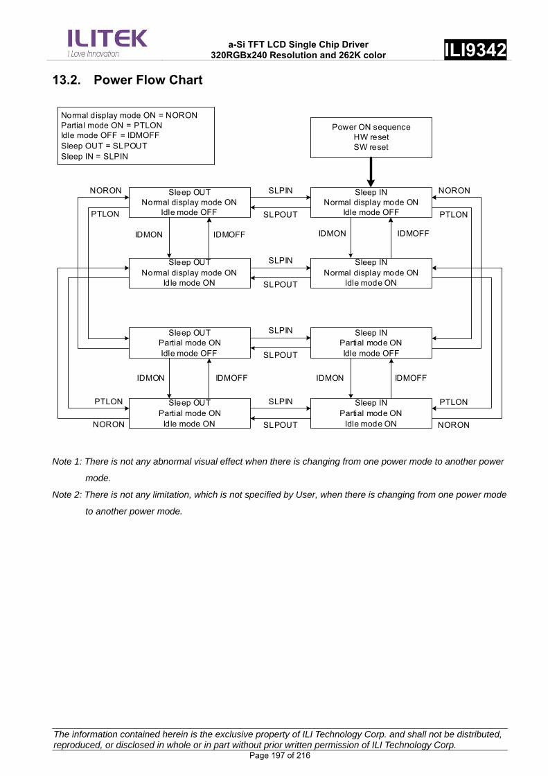
a-Si TFT LCD Single Chip Driver
320RGBx240 Resolution and 262K color ILI9342
The information contained herein is the exclusive property of ILI Technology Corp. and shall not be distributed, reproduced, or disclosed in whole or in part without prior written permission of ILI Technology Corp. Page 197 of 216
13.2. Power Flow Chart
Power ON sequence
HW resetSW reset
Sleep INNormal display mode ON
Idle mode OFF
Sleep INNormal display mode ON
Idle mode ON
Sleep INPartial mode ONIdle mode OFF
Sleep INPartial mode ON
Idle mode ON
Sleep OUTNormal display mode ON
Idle mode OFF
Sleep OUTNormal display mode ON
Idle mode ON
Sleep OUTPartial mode ONIdle mode OFF
Sleep OUTPartial mode ON
Idle mode ON
SLPIN
SLPOUT
SLPIN
SLPOUT
SLPIN
SLPOUT
SLPIN
SLPOUT
NORON
PTLON
NORON
PTLON
IDMOFFIDMON
IDMOFFIDMON
NORON
PTLON
NORON
PTLON
IDMOFFIDMON
IDMOFFIDMON
Normal display mode ON = NORONPartial mode ON = PTLONIdle mode OFF = IDMOFFSleep OUT = SLPOUTSleep IN = SLPIN
Note 1: There is not any abnormal visual effect when there is changing from one power mode to another power
mode.
Note 2: There is not any limitation, which is not specified by User, when there is changing from one power mode
to another power mode.
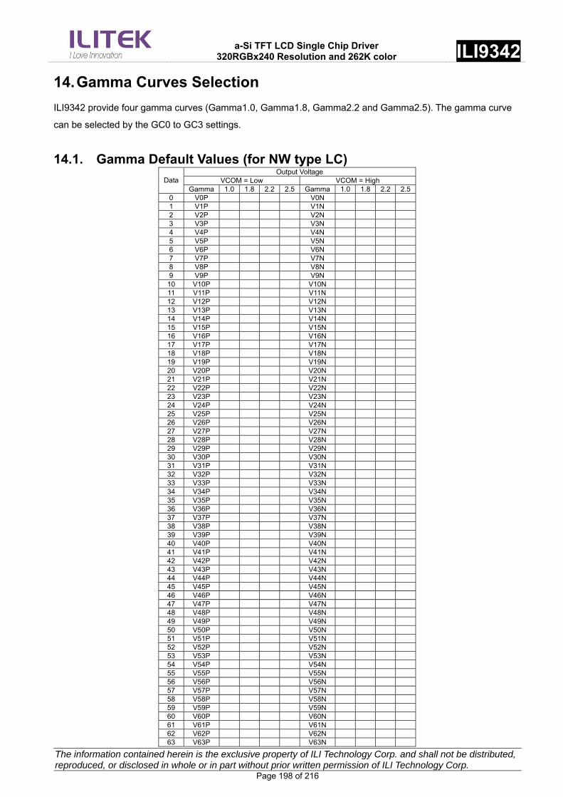
a-Si TFT LCD Single Chip Driver
320RGBx240 Resolution and 262K color ILI9342
The information contained herein is the exclusive property of ILI Technology Corp. and shall not be distributed, reproduced, or disclosed in whole or in part without prior written permission of ILI Technology Corp. Page 198 of 216
14. Gamma Curves Selection
ILI9342 provide four gamma curves (Gamma1.0, Gamma1.8, Gamma2.2 and Gamma2.5). The gamma curve
can be selected by the GC0 to GC3 settings.
14.1. Gamma Default Values (for NW type LC) Output Voltage
VCOM = Low VCOM = High Data Gamma 1.0 1.8 2.2 2.5 Gamma 1.0 1.8 2.2 2.5
0 V0P V0N 1 V1P V1N 2 V2P V2N 3 V3P V3N 4 V4P V4N 5 V5P V5N 6 V6P V6N 7 V7P V7N 8 V8P V8N 9 V9P V9N
10 V10P V10N 11 V11P V11N 12 V12P V12N 13 V13P V13N 14 V14P V14N 15 V15P V15N 16 V16P V16N 17 V17P V17N 18 V18P V18N 19 V19P V19N 20 V20P V20N 21 V21P V21N 22 V22P V22N 23 V23P V23N 24 V24P V24N 25 V25P V25N 26 V26P V26N 27 V27P V27N 28 V28P V28N 29 V29P V29N 30 V30P V30N 31 V31P V31N 32 V32P V32N 33 V33P V33N 34 V34P V34N 35 V35P V35N 36 V36P V36N 37 V37P V37N 38 V38P V38N 39 V39P V39N 40 V40P V40N 41 V41P V41N 42 V42P V42N 43 V43P V43N 44 V44P V44N 45 V45P V45N 46 V46P V46N 47 V47P V47N 48 V48P V48N 49 V49P V49N 50 V50P V50N 51 V51P V51N 52 V52P V52N 53 V53P V53N 54 V54P V54N 55 V55P V55N 56 V56P V56N 57 V57P V57N 58 V58P V58N 59 V59P V59N 60 V60P V60N 61 V61P V61N 62 V62P V62N 63 V63P V63N

a-Si TFT LCD Single Chip Driver
320RGBx240 Resolution and 262K color ILI9342
The information contained herein is the exclusive property of ILI Technology Corp. and shall not be distributed, reproduced, or disclosed in whole or in part without prior written permission of ILI Technology Corp. Page 199 of 216
14.2. Gamma Curves
14.2.1. Gamma Curve 1 (GC0), applies the function y=x2.2
14.2.2. Gamma Curve 2 (GC1), applies the function y=x1.8
14.2.3. Gamma Curve 3 (GC2), applies the function y=x2.5
14.2.4. Gamma Curve 4 (GC3), applies the function y=x1.0
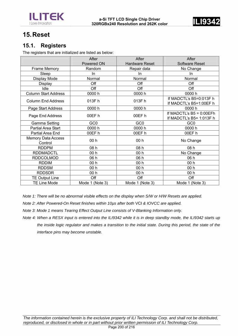
a-Si TFT LCD Single Chip Driver
320RGBx240 Resolution and 262K color ILI9342
The information contained herein is the exclusive property of ILI Technology Corp. and shall not be distributed, reproduced, or disclosed in whole or in part without prior written permission of ILI Technology Corp. Page 200 of 216
15. Reset
15.1. Registers The registers that are initialized are listed as below:
After
Powered ON After
Hardware Reset After
Software Reset Frame Memory Random Repair data No Change
Sleep In In In Display Mode Normal Normal Normal
Display Off Off Off Idle Off Off Off
Column Start Address 0000 h 0000 h 0000 h
Column End Address 013F h 013F h If MADCTL’s B5=0:013F h If MADCTL’s B5=1:00EF h
Page Start Address 0000 h 0000 h 0000 h
Page End Address 00EF h 00EF h If MADCTL’s B5 = 0:00EFh If MADCTL’s B5= 1:013F h
Gamma Setting GC0 GC0 GC0 Partial Area Start 0000 h 0000 h 0000 h Partial Area End 00EF h 00EF h 00EF h
Memory Data Access Control
00 h 00 h No Change
RDDPM 08 h 08 h 08 h RDDMADCTL 00 h 00 h No Change RDDCOLMOD 06 h 06 h 06 h
RDDIM 00 h 00 h 00 h RDDSM 00 h 00 h 00 h
RDDSDR 00 h 00 h 00 h TE Output Line Off Off Off TE Line Mode Mode 1 (Note 3) Mode 1 (Note 3) Mode 1 (Note 3)
Note 1: There will be no abnormal visible effects on the display when S/W or H/W Resets are applied.
Note 2: After Powered-On Reset finishes within 10µs after both VCI & IOVCC are applied.
Note 3: Mode 1 means Tearing Effect Output Line consists of V-Blanking Information only.
Note 4: When a RESX input is entered into the ILI9342 while it is in deep standby mode, the ILI9342 starts up
the inside logic regulator and makes a transition to the initial state. During this period, the state of the
interface pins may become unstable.
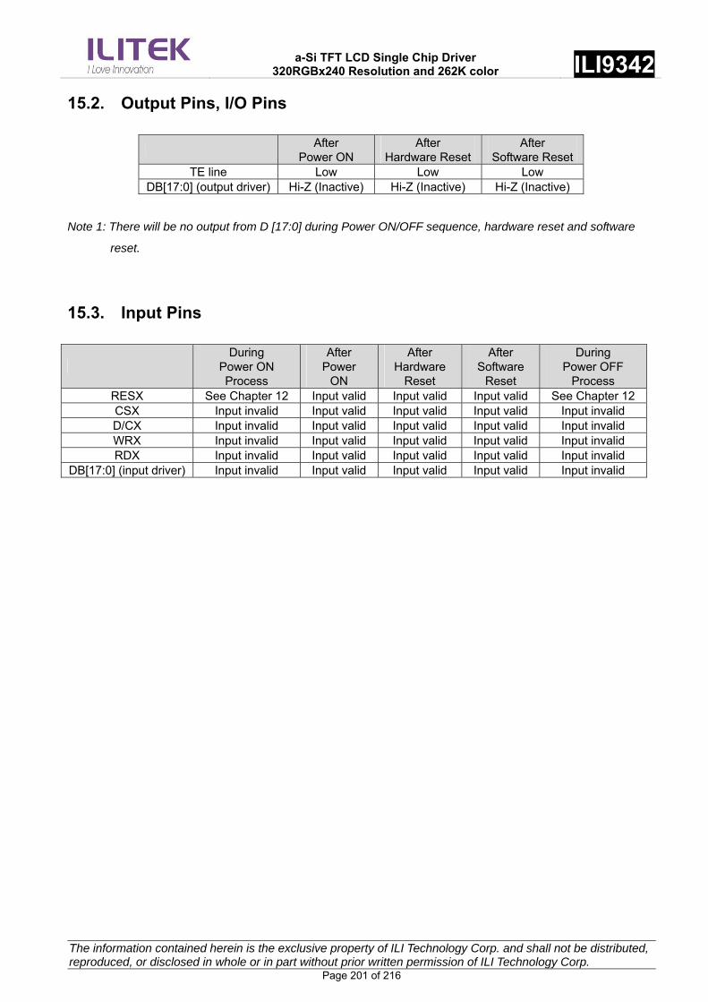
a-Si TFT LCD Single Chip Driver
320RGBx240 Resolution and 262K color ILI9342
The information contained herein is the exclusive property of ILI Technology Corp. and shall not be distributed, reproduced, or disclosed in whole or in part without prior written permission of ILI Technology Corp. Page 201 of 216
15.2. Output Pins, I/O Pins
After
Power ON After
Hardware ResetAfter
Software Reset TE line Low Low Low
DB[17:0] (output driver) Hi-Z (Inactive) Hi-Z (Inactive) Hi-Z (Inactive)
Note 1: There will be no output from D [17:0] during Power ON/OFF sequence, hardware reset and software
reset.
15.3. Input Pins
During
Power ON Process
After Power
ON
After Hardware
Reset
After Software
Reset
During Power OFF
Process RESX See Chapter 12 Input valid Input valid Input valid See Chapter 12 CSX Input invalid Input valid Input valid Input valid Input invalid D/CX Input invalid Input valid Input valid Input valid Input invalid WRX Input invalid Input valid Input valid Input valid Input invalid RDX Input invalid Input valid Input valid Input valid Input invalid
DB[17:0] (input driver) Input invalid Input valid Input valid Input valid Input invalid

a-Si TFT LCD Single Chip Driver
320RGBx240 Resolution and 262K color ILI9342
The information contained herein is the exclusive property of ILI Technology Corp. and shall not be distributed, reproduced, or disclosed in whole or in part without prior written permission of ILI Technology Corp. Page 202 of 216
15.4. Reset Timing
Shorter than 5ustRW
tRT
ResettingNormal operationInitial condition
(Default for H/W reset)
RESX
Display Status
Signal Symbol Parameter Min Max Unit RESX tRW Reset pulse duration 10 uS
5
(note 1,5) mS
tRT Reset cancel
120 (note 1,6,7)
mS
Note 1: The reset cancel includes also required time for loading ID bytes, VCOM setting and other settings from
NV memory to registers. This loading is done every time when there is HW reset cancel time (tRT)
within 5 ms after a rising edge of RESX.
Note 2: Spike due to an electrostatic discharge on RESX line does not cause irregular system reset according to
the table below: -
RESX Pulse Action
Shorter than 5us Reset Rejected
Longer than 10us Reset
Between 5us and 10us Reset starts
Note 3: During the Resetting period, the display will be blanked (The display is entering blanking sequence,
which maximum time is 120 ms, when Reset Starts in Sleep Out –mode. The display remains the blank
state in Sleep In -mode.) And then return to Default condition for Hardware Reset.
Note 4: Spike Rejection also applies during a valid reset pulse as shown below:
Note 5: When Reset applied during Sleep In Mode.
Note 6: When Reset applied during Sleep Out Mode.
Note 7: It is necessary to wait 5msec after releasing RESX before sending commands. Also Sleep Out
command cannot be sent for 120msec.

a-Si TFT LCD Single Chip Driver
320RGBx240 Resolution and 262K color ILI9342
The information contained herein is the exclusive property of ILI Technology Corp. and shall not be distributed, reproduced, or disclosed in whole or in part without prior written permission of ILI Technology Corp. Page 203 of 216
16. NV Memory Programming Flow
Start
Reset
Check (D2h)ID3_CNT/ID2_CNTID1_CNT/VMF_CNT
=3'b111
Supply External5.0V to VPP
Wait 10ms
Wait 10ms
Cut Off External7.0V Power
Reset
End
Y
NV Memory Protection Key (D1h)1st Parameter : 55h2nd Parameter : AAh3rd Parameter : 66h
NV Memory Write (D0h)1st Parameter : PGM_ADR[2:0]=3'bxxx2nd Parameter : PGM_DATA[7:0]=8'bxx
(xx=8 bit OTP value)
N

a-Si TFT LCD Single Chip Driver
320RGBx240 Resolution and 262K color ILI9342
The information contained herein is the exclusive property of ILI Technology Corp. and shall not be distributed, reproduced, or disclosed in whole or in part without prior written permission of ILI Technology Corp. Page 204 of 216
17. Deep Standby Mode Setting
Set RB7h:DSTB = 1
Display Off Sequence
Deep Standby Mode
Enter Deep Standby mode
Set CSX pin = Low, thenSet CSX pin = High
Set CSX pin = Low, thenSet CSX pin = High
Set CSX pin = Low, thenSet CSX pin = High
Set CSX pin = Low, thenSet CSX pin = High
Set CSX pin = Low, thenSet CSX pin = High
Set CSX pin = Low, thenSet CSX pin = High
Registers set as default value
ILI9340's register settingGRAM data setting
Release from Deep Standby mode
Display On Sequence
Set CSX pin low to high x 6
Note: (1) To Return display mode according to normal display ON sequence when ILI9342 exits Deep standby
mode to Sleep mode.
(2) Leave at lease 1ms between the 2nd and 3rd inputs of CSX=Low.
(3) This sequence must be completed before writing data to GRAM.
(4) ILI9342 exits deep standby mode and enters to sleep mode when an effective RESX pulse is inputted
during Deep Standby mode.

a-Si TFT LCD Single Chip Driver
320RGBx240 Resolution and 262K color ILI9342
The information contained herein is the exclusive property of ILI Technology Corp. and shall not be distributed, reproduced, or disclosed in whole or in part without prior written permission of ILI Technology Corp. Page 205 of 216
18. Electrical Characteristics
18.1. Absolute Maximum Ratings The absolute maximum rating is listed on following table. When ILI9342 is used out of the absolute maximum
ratings, ILI9342 may be permanently damaged. To use ILI9342 within the following electrical characteristics
limitation is strongly recommended for normal operation. If these electrical characteristic conditions are
exceeded during normal operation, ILI9342 will malfunction and cause poor reliability.
Item Symbol Unit Value Supply voltage VCI V -0.3 ~ +4.8 Supply voltage (Logic) IOVCC V -0.3 ~ +3.3 Supply voltage (Digital) VCORE V -0.3 ~ +2.4 Driver supply voltage VGH-VGL V -0.3 ~ +32.0 Logic input voltage range VIN V -0.3 ~ IOVCC + 0.3 Logic output voltage range VO V -0.3 ~ IOVCC + 0.3 Operating temperature Topr ℃ -40 ~ +85 Storage temperature Tstg ℃ -55 ~ +110
Note: If the absolute maximum rating of even is one of the above parameters is exceeded even momentarily, the
quality of the product may be degraded. Absolute maximum ratings, therefore, specify the values
exceeding which the product may be physically damaged. Be sure to use the product within the range of
the absolute maximum ratings.

a-Si TFT LCD Single Chip Driver
320RGBx240 Resolution and 262K color ILI9342
The information contained herein is the exclusive property of ILI Technology Corp. and shall not be distributed, reproduced, or disclosed in whole or in part without prior written permission of ILI Technology Corp. Page 206 of 216
18.2. DC Characteristics
18.2.1. General DC Characteristics Item Symbol Unit Condition Min. Typ. Max. Note
Power and Operation Voltage Analog Operating Voltage
VCI V Operating voltage 2.3 2.8 4.8 Note2
Logic Operating Voltage
IOVCC V I/O supply voltage 1.65 2.8 3.3 Note2
Digital Operating voltage
VCORE V Digital supply
voltage - 1.8 - Note2
Gate Driver High Voltage
VGH V - 10.0 - 16.0 Note3
Gate Driver Low Voltage
VGL V - -16.0 - -9.0 Note3
Driver Supply Voltage
- V |VGH-VGL| 19 - 32 Note3
Input and Output Logic High Level Input Voltage
VIH V - 0.8*IOVCC - IOVCC Note1,2,3
Logic Low Level Input Voltage
VIL V - DGND - 0.2*IOVCC Note1,2,3
Logic High Level Output Voltage
VOH V IOL=-1.0mA 0.8*IOVCC - IOVCC Note1,2,3
Logic Low Level Output Voltage
VOL V IOL=1.0mA DGND - 0.2*IOVCC Note1,2,3
Logic Input Leakage Current
ILEA uA VIN=IOVCC or
DGND -0.1 - +0.1 Note1,2,3
VCOM Operation VCOM High Voltage VCOMH V Ccom=12nF 2.5 - 5.0 Note3 VCOM Low Voltage VCOML V Ccom=12nF -2.5 - 0.0 Note3 VCOM Amplitude Voltage
VCOM V |VCOMH-VCOML| 4.0 - 5.5 Note3
Source Driver Source Output Range
Vsout V - 0.1 - DDVDH-0.1 Note4
Gamma Reference Voltage
VREG1OUT V - 3.0 - 5.0 Note3
Note 1: IOVCC=1.65 to 3.3V, VCI=2.3 to 4.8V, AGND=DGND=0V, Ta= -40 to 85 °C °C.
Note2: Please supply digital IOVCC voltage equal or less than analog VCI voltage.
Note3: CSX, RDX, WRX, DB[17:0], D/CX, RESX, TE, DOTCLK, VSYNC, HSYNC, DE, SDA, SCL, IM3, IM2, IM1,
IM0, and Test pins.
Note4: When the measurements are performed with LCD module. Measurement Points are like Note3.
Note5: Source channel loading = 10pF/channel, Gate channel loading = 50pF/channel

a-Si TFT LCD Single Chip Driver
320RGBx240 Resolution and 262K color ILI9342
The information contained herein is the exclusive property of ILI Technology Corp. and shall not be distributed, reproduced, or disclosed in whole or in part without prior written permission of ILI Technology Corp. Page 207 of 216
18.3. AC Characteristics 18.3.1. Display Parallel 18/16/9/8-bit Interface Timing Characteristics (8080-system)
tast
DCX
CSX
WRX
D[17:0](Write)
RDX
D[17:0](Read)
tcs
twrl
tcsf
twrh
twc
taht
tdst tdht
tast trcs / trcsfm
trc / trcfmtrdl / trdlfm
trdh / trdhfm
taht
trat / tratfmtrodh
tchw tchw
tcsf
Signal Symbol Parameter min max Unit Description tast Address setup time 0 - ns
DCX that Address hold time (Write/Read) 10 - ns tchw CSX “H” pulse width 0 - ns tcs Chip Select setup time (Write) 15 - ns trcs Chip Select setup time (Read ID) 45 - ns
trcsfm Chip Select setup time (Read FM) 355 - ns
CSX
tcsf Chip Select Wait time (Write/Read) 10 - ns twc Write cycle 66 ns twrh Write Control pulse H duration 33 - ns WRX
twrl Write Control pulse L duration 33 - ns trc Read cycle (ID) 160 - ns trdh Read Control pulse H duration 90 - ns RDX (ID)
trdl Read Control pulse L duration 45 - ns
When read ID data
trcfm Read Cycle (FM) 450 - ns trdhfm Read Control H duration (FM) 90 - ns RDX (FM)
trdlfm Read Control L duration (FM) 355 - ns
When read from the frame memory
tdst Write data setup time 10 - ns tdht Write data hold time 10 - ns trat Read access time - 40 ns
tratfm Read access time - 340 ns
DB[17:0], DB[15:0], DB[8:0], DB[7:0]
trod Read output disable time 20 80 ns
For maximum CL=30pF For minimum CL=8pF
Note: Ta = -40 to 85 °C, IOVCC=1.65V to 3.3V, VCI=2.3V to 4.8V, DGND=0V
tr≦15ns
70%
30%
70%
30%
tf≦15ns

a-Si TFT LCD Single Chip Driver
320RGBx240 Resolution and 262K color ILI9342
The information contained herein is the exclusive property of ILI Technology Corp. and shall not be distributed, reproduced, or disclosed in whole or in part without prior written permission of ILI Technology Corp. Page 208 of 216
CSX timings :
CSX
WRX,RDX
Min. 5nstcsf
tchw
Note: Logic high and low levels are specified as 30% and 70% of IOVCC for Input signals.
Write to read or read to write timings:
twrhtrdh
trdhfm
CSX
WRX
RDX
`0'
Note: Logic high and low levels are specified as 30% and 70% of IOVCC for Input signals.

a-Si TFT LCD Single Chip Driver
320RGBx240 Resolution and 262K color ILI9342
The information contained herein is the exclusive property of ILI Technology Corp. and shall not be distributed, reproduced, or disclosed in whole or in part without prior written permission of ILI Technology Corp. Page 209 of 216
18.3.2. Display Parallel 18/16/9/8-bit Interface Timing Characteristics (6800-system)
18.3.3. Fixed E Mode
tas
D/CX
CSX
RWX
D[17:0](wrtie)
D[17:0](Read)
tcycle
tah
tcycle / 2
tas
tDS
tOHtACC
tah
tDH
E
Fixed E Mode
Signal Symbol Parameter min max Unit Description
tas Address Setup time 10 - ns - DCX
tah Address hold Time (Write/Read) 10 - ns -
tas Address Setup time 10 - ns - R/WX
tah Address hold Time (Write/Read) 10 - ns -
CSX tcycle System Clock Cycle Time 50 790 ns -
tDS Data Setup Time 15 - ns -
tDH Data Hold Time 25 - ns tACC Data Access Time 10 - ns
D[23:0]
tOH Output Hold Time 10 - ns
For maximum CL=30pF For minimum CL=8pF
Note: (1) Ta = -40 to 85 °C, IOVCC=1.65V to 3.3V, VCI=2.3V to 4.8V, AGND=DGND=0V
(2) Does not include signal rise and fall times.
tr≦15ns
70%
30%
70%
30%
tf≦15ns

a-Si TFT LCD Single Chip Driver
320RGBx240 Resolution and 262K color ILI9342
The information contained herein is the exclusive property of ILI Technology Corp. and shall not be distributed, reproduced, or disclosed in whole or in part without prior written permission of ILI Technology Corp. Page 210 of 216
18.3.4. Clocked E Mode
tas
D/CX
E
RWX
D[17:0](wrtie)
D[17:0](Read)
tcycle
tah
tas
tDS
tOHtACC
tDH
CSX
tcycle / 2
Clocked E Mode
Signal Symbol Parameter min max Unit Description
tas Address Setup time 10 - ns - DCX
tah Address hold Time (Write/Read) 10 - ns -
tas Address Setup time 10 - ns - R/WX
tah Address hold Time (Write/Read) 10 - ns - E tcycle System Clock Cycle Time 50 790 ns -
tDS Data Setup Time 15 - ns - tDH Data Hold Time 25 - ns tACC Data Access Time 10 - ns
D[23:0]
tOH Output Hold Time 10 - ns
For maximum CL=30pF For minimum CL=8pF
Note: (1) Ta = -40 to 85 °C, IOVCC=1.65V to 3.3V, VCI=2.3V to 4.8V, AGND=DGND=0V
(2) Does not include signal rise and fall times.
tr≦15ns
70%
30%
70%
30%
tf≦15ns
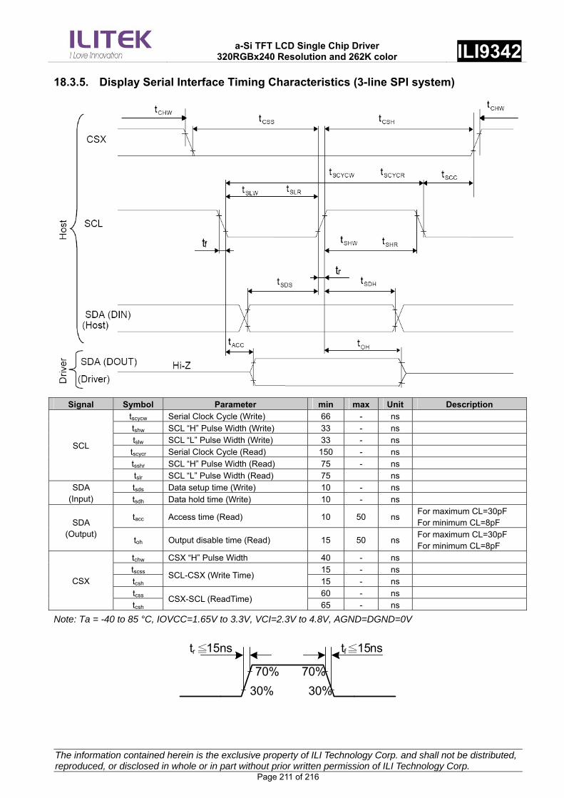
a-Si TFT LCD Single Chip Driver
320RGBx240 Resolution and 262K color ILI9342
The information contained herein is the exclusive property of ILI Technology Corp. and shall not be distributed, reproduced, or disclosed in whole or in part without prior written permission of ILI Technology Corp. Page 211 of 216
18.3.5. Display Serial Interface Timing Characteristics (3-line SPI system)
Signal Symbol Parameter min max Unit Description tscycw Serial Clock Cycle (Write) 66 - ns tshw SCL “H” Pulse Width (Write) 33 - ns tslw SCL “L” Pulse Width (Write) 33 - ns
tscycr Serial Clock Cycle (Read) 150 - ns tsshr SCL “H” Pulse Width (Read) 75 - ns
SCL
tslr SCL “L” Pulse Width (Read) 75 ns tsds Data setup time (Write) 10 - ns SDA
(Input) tsdh Data hold time (Write) 10 - ns
tacc Access time (Read) 10 50 ns For maximum CL=30pF For minimum CL=8pF SDA
(Output) toh Output disable time (Read) 15 50 ns
For maximum CL=30pF For minimum CL=8pF
tchw CSX “H” Pulse Width 40 - ns tscss 15 - ns tcsh
SCL-CSX (Write Time) 15 - ns
tcss 60 - ns
CSX
tcsh CSX-SCL (ReadTime)
65 - ns
Note: Ta = -40 to 85 °C, IOVCC=1.65V to 3.3V, VCI=2.3V to 4.8V, AGND=DGND=0V
tr≦15ns
70%
30%
70%
30%
tf≦15ns

a-Si TFT LCD Single Chip Driver
320RGBx240 Resolution and 262K color ILI9342
The information contained herein is the exclusive property of ILI Technology Corp. and shall not be distributed, reproduced, or disclosed in whole or in part without prior written permission of ILI Technology Corp. Page 212 of 216
18.3.6. Display Serial Interface Timing Characteristics (4-line SPI system)
tcss
CSX
D/CX
SCL
SDA (DIN)
SDA (DOUT)
tcsh
tas tah
twrl/trdl twrh/trdh
twc/trc
tacc tod
tdhtds
Signal Symbol Parameter min max Unit Description
tcss Chip select time (Write) 15 - Ns CSX
tcssh Chip select hold time (write) 15 - Ns twc Serial clock cycle (Write) 66 - Ns twrh SCL “H” pulse width (Write) 33 - Ns twrl SCL “L” pulse width (Write) 33 - Ns
trc Serial clock cycle (Read) 150 - Ns
trdh SCL “H” pulse width (Read) 75 - Ns
SCL
trdl SCL “L” pulse width (Read) 75 - Ns
tas D/CX setup time 10 - Ns D/CX tah D/CX hold time (Write / Read) 10 - Ns
tds Data setup time (Write) 10 - Ns SDA (Input) tdh Data hold time (Write) 10 - Ns
tacc Access time (Read) 10 50 Ns SDA (Output) tod Output disable time (Read) 15 50 Ns
For maximum CL=30pF For minimum CL=8pF
Note: Ta = -40 to 85 °C, IOVCC=1.65V to 3.3V, VCI=2.3V to 4.8V, AGND=DGND=0V
tr≦15ns
70%
30%
70%
30%
tf≦15ns

a-Si TFT LCD Single Chip Driver
320RGBx240 Resolution and 262K color ILI9342
The information contained herein is the exclusive property of ILI Technology Corp. and shall not be distributed, reproduced, or disclosed in whole or in part without prior written permission of ILI Technology Corp. Page 213 of 216
18.3.7. Parallel RGB Interface Timing Characteristics
trgbftrgbr
tSYNCS
VIH
VIL
tENS tENH
trgbrtrgbf
tPDHtPDS
tCYCD
PWDL PWDH
VIH
VIH
VIH VIH
VIH VIH
VIH
VIL VIL
VIL
VIL
VIL
VIL
VSYNCHSYNC
ENABLE
Write Data
DOTCLK
D[17:0]
Signal Symbol Parameter min max Unit Description tSYNCS VSYNC/HSYNC setup time 15 - ns VSYNC /
HSYNC tSYNCH VSYNC/HSYNC hold time 15 - ns
tENS DE setup time 15 - ns DE
tENH DE hold time 15 - ns tPOS Data setup time 15 - ns
DB[17:0] tPDH Data hold time 15 - ns
PWDH DOTCLK high-level period 33 - ns PWDL DOTCLK low-level period 33 - ns tCYCD DOTCLK cycle time 66 - ns
DOTCLK
trgbr , trgbf DOTCLK,HSYNC,VSYNC rise/fall time - 15 ns
18/16-bit bus RGB interface mode
tSYNCS VSYNC/HSYNC setup time 15 - ns VSYNC / HSYNC tSYNCH VSYNC/HSYNC hold time 15 - ns
tENS DE setup time 15 - ns DE
tENH DE hold time 15 - ns tPOS Data setup time 15 - ns
DB[17:0] tPDH Data hold time 15 - ns
PWDH DOTCLK high-level pulse period 33 - ns PWDL DOTCLK low-level pulse period 33 - ns tCYCD DOTCLK cycle time 66 - ns
DOTCLK
trgbr , trgbf DOTCLK,HSYNC,VSYNC rise/fall time - 15 ns
6-bit bus RGB interface mode
Note: Ta = -40 to 85 °C, IOVCC=1.65V to 3.3V, VCI=2.3V to 4.8V, AGND=DGND=0V
tr≦15ns
70%
30%
70%
30%
tf≦15ns
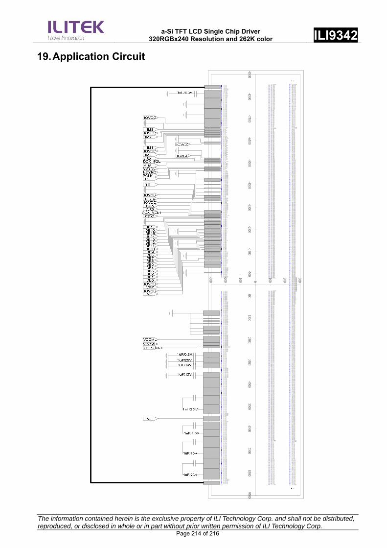
a-Si TFT LCD Single Chip Driver
320RGBx240 Resolution and 262K color ILI9342
The information contained herein is the exclusive property of ILI Technology Corp. and shall not be distributed, reproduced, or disclosed in whole or in part without prior written permission of ILI Technology Corp. Page 214 of 216
19. Application Circuit
1 V C O M2 V C O M3 V C O M4 V C O M5 D U MMY R 16 D U MMY R 27 V C O R E8 V C O R E9 V C O R E10 V C O R E11 V C O R E12 V C O R E13 V C O R E14 V C O R E15 A G N D16 A G N D17 A G N D18 A G N D19 A G N D20 A G N D21 A G N D22 A G N D23 A G N D24 A G N D25 A G N D26 A G N D27 D G N D28 D G N D29 D G N D30 D G N D31 D G N D32 D G N D33 D G N D34 D G N D35 D G N D36 D G N D37 D G N D38 D G N D39 IO V C C40 IO V C C41 IO V C C42 IO V C C43 IO V C C44 IO V C C45 IO V C C46 IO V C C47 IO V C C48 IO V C C49 D U MMY50 D G N D51 IM352 IO V C C53 IM254 D G N D55 IM156 IO V C C57 IM058 D G N D59 D G N D60 TEST_EN61 TEST_O SC62 TEST863 D U MMY64 D U MMY65 D G N D66 D U MMY67 IO V C C68 TEST769 D U MMY70 TEST671 D U MMY72 TEST573 D U MMY74 TEST475 D U MMY76 TEST377 D U MMY78 TEST279 D U MMY80 TEST181 D U MMY82 TEST083 D G N D84 D U MMY85 IO V C C86 C SX87 D C X _SC L88 SD A89 D U MMY90 D U MMY91 D U MMY92 D U MMY93 V SY N C94 H SY N C95 PC LK96 D E97 D G N D98 D U MMY99 D U MMY100 D U MMY101 D U MMY102 D U MMY103 D U MMY104 D U MMY105 D U MMY106 D G N D107 D G N D108 D G N D109 D G N D110 D U MMY111 D U MMY112 D U MMY113 D G N D114 D U MMY115 D U MMY116 D U MMY117 D G N D118 D U MMY119 D U MMY120 D U MMY121 D G N D122 D U MMY123 D U MMY124 D U MMY125 D G N D126 TE127 TE128 D G N D129 D U MMY130 IO V C C131 D U MMY132 D G N D133 R ESX134 D U MMY135 D U MMY136 D U MMY137 D U MMY138 D U MMY139 D U MMY140 D U MMY141 D U MMY142 IO V C C143 IO V C C144 IO V C C145 IO V C C146 R D X147 W R X148 D C X _SC L1149 C SX 1150 D G N D151 D B 17152 D B 17153 D B 16154 D B 16155 D B 15156 D B 15157 D B 14158 D B 14159 D B 13160 D B 13161 D B 12162 D B 12163 D G N D164 D B 11165 D B 11166 D B 10167 D B 10168 D B 9169 D B 9170 D B 8171 D B 8172 D B 7173 D B 7174 D B 6175 D B 6176 D G N D177 D B 5178 D B 5179 D B 4180 D B 4181 D B 3182 D B 3183 D B 2184 D B 2185 D B 1186 D B 1187 D B 0188 D B 0189 IO V C C190 D U MMY191 D G N D192 D G N D193 D G N D194 D G N D195 V PP196 V PP197 V PP198 D U MMY199 IO V C C200 IO V C C201 IO V C C202 IO V C C203 V C I204 V C I205 V C I206 V C I207 D U MMY208 D U MMY209 D U MMY210 D U MMY211 TESTO 1212 D G N D213 G PIO 0214 G PIO 0215 G PIO 1216 G PIO 1217 D U MMY218 TESTO 2
219 G PIO 2220 G PIO 2221 G PIO 3222 G PIO 3223 G PIO 4224 G PIO 4225 G PIO 5226 G PIO 5227 G PIO 6228 G PIO 6229 G PIO 7230 G PIO 7231 D U MMY232 D U MMY233 D U MMY234 D U MMY235 D U MMY236 D U MMY237 D U MMY238 D U MMY239 D U MMY240 D U MMY241 D G N D242 D G N D243 D G N D244 D G N D245 D G N D246 D G N D247 D U MMY248 D U MMY249 D G N D250 D U MMY251 D U MMY252 D G N D253 D U MMY254 D U MMY255 D G N D256 D U MMY257 D U MMY258 D G N D259 D G N D260 D G N D261 D G N D262 D G N D263 A G N D264 A G N D265 A G N D266 A G N D267 V G S268 D U MMY269 D U MMY270 D U MMY271 D U MMY272 D U MMY273 D U MMY274 D U MMY275 D U MMY276 D U MMY277 D U MMY278 D U MMY279 D U MMY280 D U MMY281 V R EG 1_O U T282 V R EG 1_O U T283 D U MMY284 D U MMY285 D U MMY286 D U MMY287 D U MMY288 V C L289 V C L290 V C L291 V C L292 V C L293 V C L294 V G H295 V G H296 V G H297 V G H298 V G H299 V G H300 V G L301 V G L302 V G L303 V G L304 V G L305 V G L306 D U MMY307 D U MMY308 D U MMY309 D U MMY310 D U MMY311 D D V D H312 D D V D H313 D D V D H314 D D V D H315 D D V D H316 D D V D H317 C 12N318 C 12N319 C 12N320 C 12N321 C 12N322 C 12N323 C 12N324 C 12N325 C 12N326 C 12N327 C 12P328 C 12P329 C 12P330 C 12P331 C 12P332 C 12P333 C 12P334 C 12P335 C 12P336 C 12P337 C 11N338 C 11N339 C 11N340 C 11N341 C 11N342 C 11N343 C 11N344 C 11N345 C 11N346 C 11N347 C 11P348 C 11P349 C 11P350 C 11P351 C 11P352 C 11P353 C 11P354 C 11P355 C 11P356 C 11P357 D U MMY358 D U MMY359 D U MMY360 V C I361 V C I362 V C I363 V C I364 V C I365 V C I366 D U MMY367 C 31N368 C 31N369 C 31N370 C 31N371 C 31N372 C 31N373 C 31N374 C 31N375 C 31P376 C 31P377 C 31P378 C 31P379 C 31P380 C 31P381 C 31P382 C 31P383 C 21N384 C 21N385 C 21N386 C 21N387 C 21N388 C 21N389 C 21N390 C 21N391 C 21N392 C 21N393 C 21N394 C 21N395 C 21P396 C 21P397 C 21P398 C 21P399 C 21P400 C 21P401 C 21P402 C 21P403 C 21P404 C 21P405 C 21P406 C 21P407 C 22N408 C 22N409 C 22N410 C 22N411 C 22N412 C 22N413 C 22N414 C 22N415 C 22N416 C 22N417 C 22N418 C 22N419 C 22P420 C 22P421 C 22P422 C 22P423 C 22P424 C 22P425 C 22P426 C 22P427 C 22P428 C 22P429 C 22P430 C 22P431 D U MMY R 3432 D U MMY R 4433 V C O M434 V C O M435 V C O M436 V C O M
437 D U MMY438 D U MMY 439 G 240440 G 238 441 G 236442 G 234 443 G 232444 G 230 445 G 228446 G 226 447 G 224448 G 222 449 G 220450 G 218 451 G 216452 G 214 453 G 212454 G 210 455 G 208456 G 206 457 G 204458 G 202 459 G 200460 G 198 461 G 196462 G 194 463 G 192464 G 190 465 G 188466 G 186 467 G 184468 G 182 469 G 180470 G 178 471 G 176472 G 174 473 G 172474 G 170 475 G 168476 G 166 477 G 164478 G 162 479 G 160480 G 158 481 G 156482 G 154 483 G 152484 G 150 485 G 148486 G 146 487 G 144488 G 142 489 G 140490 G 138 491 G 136492 G 134 493 G 132494 G 130 495 G 128496 G 126 497 G 124498 G 122 499 G 120500 G 118 501 G 116502 G 114 503 G 112504 G 110 505 G 108506 G 106 507 G 104508 G 102 509 G 100510 G 98 511 G 96512 G 94 513 G 92514 G 90 515 G 88516 G 86 517 G 84518 G 82 519 G 80520 G 78 521 G 76522 G 74 523 G 72524 G 70 525 G 68526 G 66 527 G 64528 G 62 529 G 60530 G 58 531 G 56532 G 54 533 G 52534 G 50 535 G 48536 G 46 537 G 44538 G 42 539 G 40540 G 38 541 G 36542 G 34 543 G 32544 G 30 545 G 28546 G 26 547 G 24548 G 22 549 G 20550 G 18 551 G 16552 G 14 553 G 12554 G 10 555 G 8556 G 6 557 G 4558 G 2 559 D U MMY560 D U MMY 561 D U MMY562 D U MMY 563 S960564 S959 565 S958566 S957 567 S956568 S955 569 S954570 S953 571 S952572 S951 573 S950574 S949 575 S948576 S947 577 S946578 S945 579 S944580 S943 581 S942582 S941 583 S940584 S939 585 S938586 S937 587 S936588 S935 589 S934590 S933 591 S932592 S931 593 S930594 S929 595 S928596 S927 597 S926598 S925 599 S924600 S923 601 S922602 S921 603 S920604 S919 605 S918606 S917 607 S916608 S915 609 S914610 S913 611 S912612 S911 613 S910614 S909 615 S908616 S907 617 S906618 S905 619 S904620 S903 621 S902622 S901 623 S900624 S899 625 S898626 S897 627 S896628 S895 629 S894630 S893 631 S892632 S891 633 S890634 S889 635 S888636 S887 637 S886638 S885 639 S884640 S883 641 S882642 S881 643 S880644 S879 645 S878646 S877 647 S876648 S875 649 S874650 S873 651 S872652 S871 653 S870654 S869 655 S868656 S867 657 S866658 S865 659 S864660 S863 661 S862662 S861 663 S860664 S859 665 S858666 S857 667 S856668 S855 669 S854670 S853 671 S852672 S851 673 S850674 S849 675 S848676 S847 677 S846678 S845 679 S844680 S843 681 S842682 S841 683 S840684 S839 685 S838686 S837 687 S836688 S835 689 S834690 S833 691 S832692 S831 693 S830694 S829 695 S828696 S827 697 S826698 S825 699 S824700 S823 701 S822702 S821 703 S820704 S819 705 S818706 S817 707 S816708 S815 709 S814710 S813 711 S812712 S811 713 S810714 S809 715 S808716 S807 717 S806718 S805 719 S804720 S803 721 S802722 S801 723 S800724 S799 725 S798726 S797 727 S796728 S795 729 S794730 S793 731 S792732 S791 733 S790734 S789 735 S788736 S787 737 S786738 S785 739 S784740 S783 741 S782742 S781 743 S780744 S779 745 S778746 S777 747 S776748 S775 749 S774750 S773 751 S772752 S771 753 S770754 S769 755 S768756 S767 757 S766758 S765 759 S764760 S763 761 S762762 S761 763 S760764 S759 765 S758766 S757 767 S756768 S755 769 S754770 S753 771 S752772 S751 773 S750774 S749 775 S748776 S747 777 S746778 S745 779 S744780 S743 781 S742782 S741 783 S740784 S739 785 S738786 S737 787 S736788 S735 789 S734790 S733 791 S732792 S731 793 S730794 S729 795 S728796 S727 797 S726798 S725 799 S724800 S723 801 S722802 S721 803 S720804 S719 805 S718806 S717 807 S716808 S715 809 S714810 S713 811 S712812 S711 813 S710814 S709 815 S708816 S707 817 S706818 S705 819 S704820 S703 821 S702822 S701 823 S700824 S699 825 S698826 S697 827 S696828 S695 829 S694830 S693 831 S692832 S691 833 S690834 S689 835 S688836 S687 837 S686838 S685 839 S684840 S683 841 S682842 S681 843 S680844 S679 845 S678846 S677 847 S676848 S675 849 S674850 S673 851 S672852 S671 853 S670854 S669 855 S668856 S667 857 S666858 S665 859 S664860 S663 861 S662862 S661 863 S660864 S659 865 S658866 S657 867 S656868 S655 869 S654870 S653 871 S652872 S651 873 S650874 S649 875 S648876 S647 877 S646878 S645 879 S644880 S643 881 S642882 S641 883 S640884 S639 885 S638886 S637 887 S636888 S635 889 S634890 S633 891 S632892 S631 893 S630894 S629 895 S628896 S627 897 S626898 S625 899 S624900 S623 901 S622902 S621 903 S620904 S619 905 S618906 S617 907 S616908 S615 909 S614910 S613 911 S612912 S611 913 S610914 S609 915 S608916 S607 917 S606918 S605 919 S604920 S603 921 S602922 S601 923 S600924 S599 925 S598926 S597 927 S596928 S595 929 S594930 S593 931 S592932 S591 933 S590934 S589 935 S588936 S587 937 S586938 S585 939 S584940 S583 941 S582942 S581 943 S580944 S579 945 S578946 S577 947 S576948 S575 949 S574950 S573 951 S572952 S571 953 S570954 S569 955 S568956 S567 957 S566958 S565 959 S564960 S563 961 S562962 S561 963 S560964 S559 965 S558966 S557 967 S556968 S555 969 S554970 S553 971 S552972 S551 973 S550974 S549 975 S548976 S547 977 S546978 S545 979 S544980 S543 981 S542982 S541 983 S540984 S539 985 S538986 S537 987 S536988 S535 989 S534990 S533 991 S532992 S531 993 S530994 S529 995 S528996 S527 997 S526998 S525 999 S5241000 S523 1001 S5221002 S521 1003 S5201004 S519 1005 S5181006 S517 1007 S5161008 S515 1009 S5141010 S513 1011 S5121012 S511 1013 S5101014 S509 1015 S5081016 S507 1017 S5061018 S505 1019 S5041020 S503 1021 S5021022 S501 1023 S5001024 S499 1025 S4981026 S497 1027 S4961028 S495 1029 S4941030 S493 1031 S4921032 S491 1033 S4901034 S489 1035 S4881036 S487 1037 S4861038 S485 1039 S4841040 S483 1041 S4821042 S481 1043 D U MMY1044 D U MMY 1045 D U MMY1046 D U MMY1047 D U MMY1048 D U MMY1049 D U MMY1050 D U MMY1051 D U MMY1052 D U MMY1053 D U MMY1054 D U MMY1055 D U MMY1056 D U MMY1057 D U MMY1058 D U MMY1059 D U MMY1060 D U MMY1061 D U MMY1062 D U MMY1063 D U MMY1064 D U MMY1065 D U MMY 1066 D U MMY1067 S480 1068 S4791069 S478 1070 S4771071 S476 1072 S4751073 S474 1074 S4731075 S472 1076 S4711077 S470 1078 S4691079 S468 1080 S4671081 S466 1082 S4651083 S464 1084 S4631085 S462 1086 S4611087 S460 1088 S4591089 S458 1090 S4571091 S456 1092 S4551093 S454 1094 S4531095 S452 1096 S4511097 S450 1098 S4491099 S448 1100 S4471101 S446 1102 S4451103 S444 1104 S4431105 S442 1106 S4411107 S440 1108 S4391109 S438 1110 S4371111 S436 1112 S4351113 S434 1114 S4331115 S432 1116 S4311117 S430 1118 S4291119 S428 1120 S4271121 S426 1122 S4251123 S424 1124 S4231125 S422 1126 S4211127 S420 1128 S4191129 S418 1130 S4171131 S416 1132 S4151133 S414 1134 S4131135 S412 1136 S4111137 S410 1138 S4091139 S408 1140 S4071141 S406 1142 S4051143 S404 1144 S4031145 S402 1146 S4011147 S400 1148 S3991149 S398 1150 S3971151 S396 1152 S3951153 S394 1154 S3931155 S392 1156 S3911157 S390 1158 S3891159 S388 1160 S3871161 S386 1162 S3851163 S384 1164 S3831165 S382 1166 S3811167 S380 1168 S3791169 S378 1170 S3771171 S376 1172 S3751173 S374 1174 S3731175 S372 1176 S3711177 S370 1178 S3691179 S368 1180 S3671181 S366 1182 S3651183 S364 1184 S3631185 S362 1186 S3611187 S360 1188 S3591189 S358 1190 S3571191 S356 1192 S3551193 S354 1194 S3531195 S352 1196 S3511197 S350 1198 S3491199 S348 1200 S3471201 S346 1202 S3451203 S344 1204 S3431205 S342 1206 S3411207 S340 1208 S3391209 S338 1210 S3371211 S336 1212 S3351213 S334 1214 S3331215 S332 1216 S3311217 S330 1218 S3291219 S328 1220 S3271221 S326 1222 S3251223 S324 1224 S3231225 S322 1226 S3211227 S320 1228 S3191229 S318 1230 S3171231 S316 1232 S3151233 S314 1234 S3131235 S312 1236 S3111237 S310 1238 S3091239 S308 1240 S3071241 S306 1242 S3051243 S304 1244 S3031245 S302 1246 S3011247 S300 1248 S2991249 S298 1250 S2971251 S296 1252 S2951253 S294 1254 S2931255 S292 1256 S2911257 S290 1258 S2891259 S288 1260 S2871261 S286 1262 S2851263 S284 1264 S2831265 S282 1266 S2811267 S280 1268 S2791269 S278 1270 S2771271 S276 1272 S2751273 S274 1274 S2731275 S272 1276 S2711277 S270 1278 S2691279 S268 1280 S2671281 S266 1282 S2651283 S264 1284 S2631285 S262 1286 S2611287 S260 1288 S2591289 S258 1290 S2571291 S256 1292 S2551293 S254 1294 S2531295 S252 1296 S2511297 S250 1298 S2491299 S248 1300 S2471301 S246 1302 S2451303 S244 1304 S2431305 S242 1306 S2411307 S240 1308 S2391309 S238 1310 S2371311 S236 1312 S2351313 S234 1314 S2331315 S232 1316 S2311317 S230 1318 S2291319 S228 1320 S2271321 S226 1322 S2251323 S224 1324 S2231325 S222 1326 S2211327 S220 1328 S2191329 S218 1330 S2171331 S216 1332 S2151333 S214 1334 S2131335 S212 1336 S2111337 S210 1338 S2091339 S208 1340 S2071341 S206 1342 S2051343 S204 1344 S2031345 S202 1346 S2011347 S200 1348 S1991349 S198 1350 S1971351 S196 1352 S1951353 S194 1354 S1931355 S192 1356 S1911357 S190 1358 S1891359 S188 1360 S1871361 S186 1362 S1851363 S184 1364 S1831365 S182 1366 S1811367 S180 1368 S1791369 S178 1370 S1771371 S176 1372 S1751373 S174 1374 S1731375 S172 1376 S1711377 S170 1378 S1691379 S168 1380 S1671381 S166 1382 S1651383 S164 1384 S1631385 S162 1386 S1611387 S160 1388 S1591389 S158 1390 S1571391 S156 1392 S1551393 S154 1394 S1531395 S152 1396 S1511397 S150 1398 S1491399 S148 1400 S1471401 S146 1402 S1451403 S144 1404 S1431405 S142 1406 S1411407 S140 1408 S1391409 S138 1410 S1371411 S136 1412 S1351413 S134 1414 S1331415 S132 1416 S1311417 S130 1418 S1291419 S128 1420 S1271421 S126 1422 S1251423 S124 1424 S1231425 S122 1426 S1211427 S120 1428 S1191429 S118 1430 S1171431 S116 1432 S1151433 S114 1434 S1131435 S112 1436 S1111437 S110 1438 S1091439 S108 1440 S1071441 S106 1442 S1051443 S104 1444 S1031445 S102 1446 S1011447 S100 1448 S991449 S98 1450 S971451 S96 1452 S951453 S94 1454 S931455 S92 1456 S911457 S90 1458 S891459 S88 1460 S871461 S86 1462 S851463 S84 1464 S831465 S82 1466 S811467 S80 1468 S791469 S78 1470 S771471 S76 1472 S751473 S74 1474 S731475 S72 1476 S711477 S70 1478 S691479 S68 1480 S671481 S66 1482 S651483 S64 1484 S631485 S62 1486 S611487 S60 1488 S591489 S58 1490 S571491 S56 1492 S551493 S54 1494 S531495 S52 1496 S511497 S50 1498 S491499 S48 1500 S471501 S46 1502 S451503 S44 1504 S431505 S42 1506 S411507 S40 1508 S391509 S38 1510 S371511 S36 1512 S351513 S34 1514 S331515 S32 1516 S311517 S30 1518 S291519 S28 1520 S271521 S26 1522 S251523 S24 1524 S231525 S22 1526 S211527 S20 1528 S191529 S18 1530 S171531 S16 1532 S151533 S14 1534 S131535 S12 1536 S111537 S10 1538 S91539 S8 1540 S71541 S6 1542 S51543 S4 1544 S31545 S2 1546 S11547 D U MMY 1548 D U MMY1549 D U MMY 1550 D U MMY1551 G 1 1552 G 31553 G 5 1554 G 71555 G 9 1556 G 111557 G 13 1558 G 151559 G 17 1560 G 191561 G 21 1562 G 231563 G 25 1564 G 271565 G 29 1566 G 311567 G 33 1568 G 351569 G 37 1570 G 391571 G 41 1572 G 431573 G 45 1574 G 471575 G 49 1576 G 511577 G 53 1578 G 551579 G 57 1580 G 591581 G 61 1582 G 631583 G 65 1584 G 671585 G 69 1586 G 711587 G 73 1588 G 751589 G 77 1590 G 791591 G 81 1592 G 831593 G 85 1594 G 871595 G 89 1596 G 911597 G 93 1598 G 951599 G 97 1600 G 991601 G 101 1602 G 1031603 G 105 1604 G 1071605 G 109 1606 G 1111607 G 113 1608 G 1151609 G 117 1610 G 1191611 G 121 1612 G 1231613 G 125 1614 G 1271615 G 129 1616 G 1311617 G 133 1618 G 1351619 G 137 1620 G 1391621 G 141 1622 G 1431623 G 145 1624 G 1471625 G 149 1626 G 1511627 G 153 1628 G 1551629 G 157 1630 G 1591631 G 161 1632 G 1631633 G 165 1634 G 1671635 G 169 1636 G 1711637 G 173 1638 G 1751639 G 177 1640 G 1791641 G 181 1642 G 1831643 G 185 1644 G 1871645 G 189 1646 G 1911647 G 193 1648 G 1951649 G 197 1650 G 1991651 G 201 1652 G 2031653 G 205 1654 G 2071655 G 209 1656 G 2111657 G 213 1658 G 2151659 G 217 1660 G 2191661 G 221 1662 G 2231663 G 225 1664 G 2271665 G 229 1666 G 2311667 G 233 1668 G 2351669 G 237 1670 G 2391671 D U MMY 1672 D U MMY
A 1
A 2
-300
-200
-100 0
100
200
300
-9500-8500
-7500-6500
-5500-4500
-3500-2500
-1500-500
5001500
25003500
45005500
65007500
85009500

a-Si TFT LCD Single Chip Driver
320RGBx240 Resolution and 262K color ILI9342
The information contained herein is the exclusive property of ILI Technology Corp. and shall not be distributed, reproduced, or disclosed in whole or in part without prior written permission of ILI Technology Corp. Page 215 of 216
Items Recommended Specification Pin connection
6.3V VCORE, VCL, C11P/N, C31P/N, C12P/N (Note 1)
10V DDVDH, C21P/N, C22P/N
16V VGL
Capacity 1 µF
25V VGH
Note 1 : If using 3x DDVDH setting , the C12P/N capacity should be add to application circuit.

a-Si TFT LCD Single Chip Driver
320RGBx240 Resolution and 262K color ILI9342
The information contained herein is the exclusive property of ILI Technology Corp. and shall not be distributed, reproduced, or disclosed in whole or in part without prior written permission of ILI Technology Corp. Page 216 of 216
20. Revision History
Version No. Date Page Description V001 2009/09/21 All New Created
V002 2009/12/28 17~25 Pad location table error
V003 2009/12/29 16 Pad size description
V004 2010/2/2 85 Correct Command default
V005 2010/3/3 118 Correct 33h default
16 Pad diagram
159 SAP setting correction
V006 2010/3/4 13 Testing description
V007 2010/3/17 9 Circuit block diagram
12 CSX1/D/CX_SCL1 descriptopn
215 External capacity value
V008 2010/3/31 99 Modify Sleep out restriction
150 Modify SS description
206~213 AC/DC timing revise