a review on photo luminescence and
TRANSCRIPT

8/8/2019 A Review on Photo Luminescence And
http://slidepdf.com/reader/full/a-review-on-photo-luminescence-and 1/13
Surface Technology, 26 (1985) 93 - 105 93
A REVIEW ON PHOTOLUMINESCENCE ANDELECTROLUMINESCENCE OF SEMICONDUCTORS FOR
PHOTOELECTROCHEMICAL CELLS
L. PE RALDO BICELLI
Departm ent of Applied Phy sical Chemist ry, Mil an Poly technic, Research Centre on
Electrode Processes, Consiglio N az ional e delle Ricerche, Piaz za Leonardo da Vinci 32,
20133 Milan (Italy)
(Received January 22, 1985)
Summary
This review is concerned with the photoluminescent and electrolumi-
nescent properties of semiconductor electrodes used in photoelectrochemi-cal cells for optical-to-electrical energy conversion. Luminescence notonly provides insight into the excited-state deactivation routes which arecrucial to efficient energy conversion, but also allows one to obtain in arelatively simple manner valuable information about bulk and surfaceimperfections that negatively influence photoelectrochemical performance
of the semiconductor.
1. Introduction
Solar energy represents a major source of energy for the Earth and it
can be transformed into different kinds of energy that are useful to human-ity. One of the various possible transformation methods is the conversionof solar energy into electrical energy by utilizing photovoltaic and photo-
electrochemical (PEC) cells. Both devices involve semiconductors, theformer is based on a homo- or hetero-solid-solid junction, while the latteris based on a solid-liquid junction.
There are numerous reviews (e.g., ref. 1 and references cited therein)that provide a general picture of the PEC solar cells that have been studiedand discuss the difficulties connected with photostability and low efficiencyof semiconducting electrodes. In order to obtain materials whose perfor-mance allows interesting applications, it is imperative to control all surfaceand bulk defects that act as recombination centres of the electron-holepairs.
One method of doing this is to characterize the electronic structureof the semiconductor and to examine the excited-state processes as well astheir deactivation routes, i.e. to study the photoluminescent and electrolumi-nescent properties of the semiconductor itself. In this review, luminescence
@ Elsevier Sequoia/Print ed in The Netherlands

8/8/2019 A Review on Photo Luminescence And
http://slidepdf.com/reader/full/a-review-on-photo-luminescence-and 2/13
94
from semiconductors will be discussed in connection with their PEC behav-
iour, and the basic principles will be considered by which such excited-state
processes occur. We then concentrate on the actual knowledge of and the
problems relating to photoluminescence (PL) and electroluminescence (EL).
Furthermore, PL and EL are examined as useful in situ techniques for thestudy of semiconductor-electrolyte interfaces.
Although research on light emission from semiconductors in contact
with an electrolyte dates back to the 197Os, at present there is a renewed
interest and several research groups are active in the field.
2. Theoretical considerations
2.1. Photogenerative cells
In PEC cells capable of transforming solar energy into electrical en-ergy (so-called regenerative cells), such as for example the n-CdSI S2-, S,
OH-IPt cell, the electrolyte contains a single dissolved redox couple. On
immersion of the semiconductor in the electrolytic solution there is an
exchange of electrons between the two phases until their Fermi levels, i.e.,
their electrochemical potentials, are equal. Owing to the small charge carrier
concentration in the semiconductor, the transfer process modifies the
electron concentration with respect to the bulk value in a small region,
typically 0.1 to 1 pm wide close to the interface, the so-called space-charge
region, thus producing a parallel bending of the semiconductor valence andconduction bands. In the case when the Fermi level of the redox couple
(representing its Nernst potential) is effectively situated within the semi-
conductor forbidden band at flat-band conditions, a depletion layer of the
majority carriers forms in the proximity of the junction. This implies a
simultaneous bending-down or bending-up of the bands for n-type or p-type
semiconductors respectively, whereas the Fermi level remains flat through-
out the whole material. Absorption of a photon whose energy is equal to or
greater than the band gap energy promotes an electron from the valence
band to the conduction band, while the electric field in the depletion layerseparates the electron-hole pairs thus produced, preventing their recombina-
tion. Thus, in an n-type semiconductor that is part of a PEC cell, the minor-
ity carriers (holes) move toward the electrolyte and oxidize the reduced
component of the redox couple, whereas the majority carriers (electrons)moire toward the bulk of the semiconductor and reach the counterelectrode
to produce the reverse reduction reaction. Therefore, the electrolyte com-
position remains (in principle) the same, and solar energy is converted into
electrical energy.
Although the device is theoretically expected to operate indefinitely,
the desired PEC reaction may be accompanied by other unwanted reactions,e.g. decomposition of the material. In fact, one of the major problems in
making practical PEC cells is to avoid photocorrosion of the semiconducting
electrode.

8/8/2019 A Review on Photo Luminescence And
http://slidepdf.com/reader/full/a-review-on-photo-luminescence-and 3/13
95
2.2. Luminescence
There are several methods allowing the production of luminescence
from semiconductors. In this review we mainly consider PL and EL where
the population of the emitting excited state is produced by photon absorp-
tion or by an electric current, respectively. Cathodoluminescence andtriboluminescence are also widely examined, excitation resulting from a
beam of electrons in the former case and from mechanical means in the
latter case.
2.2.1. Pho toluminescence
The mechanism by which PL is produced can easily be understood if
reference is made to the previous observations in connection with PEC
cells.
As stated above, ultraband-gap photon absorption by semiconductors
yields an electron-hole pair which according to Ellis [ 21 “can be regardedcrudely as a one-electron picture of the semiconductor’s excited state”.
In PEC cells, we have seen that these electron-hole pairs are separated in
the space-charge region and give rise to a photocurrent. Thus, the excited-
state deactivation mechanism is non-radiative. In contrast, when a radiative
recombination of the two charge carriers takes place PL is observed.
Besides radiative transitions from the bottom of the conduction band
to the top of the valence band whose emitted energy is equal to the band gap
energy, so-called edge emission [ 31, radiative intra-band gap transitions are
also possible. They involve energy levels lying within the semiconductorforbidden band and give rise to sub-band gap emission, i.e. to peaks situated
at the longer wavelength side of the edge emission peaks.
These intra-band gap levels can be distinguished in surface or near-
surface states and in deep trapping levels arising from bulk imperfections
(impurity atoms and intrinsic defects such as interstitial atoms or atom
vacancies).
Of course, non-radiative recombination of the electron-hole pairs is
also possible resulting in lattice vibration, i.e. in heat production.
2.2.2. Electroluminescence
Typical examples are n-type II-VI binary and ternary semiconducting
compounds in a PEC cell containing an aqueous, alkaline peroxydisulphate
solution [ 4 - 61. By polarizing such an electrode in the dark at potentials
cathodic of its flat-band potential, luminescence of the colour emitted
during PL experiments is observed. This is a general result with strongly
oxidizing electrolytes: bands observed in PL spectra are observed even in
EL spectra, but the reverse is not always true (see below).
As to the EL mechanism, an electron in and/or near the conduction
band is able to reduce an SZOs2 - anion in the dark to yield strongly oxi-dizing SO,; radical anions. The latter, in turn, inject holes (i.e. minority
carriers) into the valence band and/or into some intermediate levels thus
producing a cathodic current. Subsequently, radiative recombination of an

8/8/2019 A Review on Photo Luminescence And
http://slidepdf.com/reader/full/a-review-on-photo-luminescence-and 4/13
96
electron with the injected hole yields emission of band gap or sub-band gap
energy [7 - 91. Thus, the emitted EL spectrum is a consequence of the
charge-transfer process across the interface, and EL continues until the
oxidizing agent in the solution is completely consumed. Usually, to avoid
EL intensity decay from the initial value, the electrode is continuouslypulsed between a potential where no current is observed and a potential
sufficiently cathodic to initiate EL, while the spectrometer is scanned at
constant speed. In addition, the electrolyte is thoroughly stirred. Some evi-
dence for competitive electrode reduction has also been presented [ 9 - 111.
EL has been observed with a variety of oxidized components of redox
couples, e.g. Fe( CN)6 3- for n-Gap [7,12], and, more recently, Fe3+, Ce4+
and again Fe(CN), 3- for n-GaAs [ 13 - 151. Using one-electron redox cou-
ples, the energetic conditions for hole injection into and/or near the valence
band can be analyzed more carefully than in cases where the injecting
species is a highly active intermediate (e.g. SO,-) whose energy level distribu-
tion is poorly defined.
2.3. Comparisons
In agreement with the above, EL takes place when the semiconductor
bands are in light accumulation conditions very close to flat-band conditions
(i.e. small upward bending for n-type materials) and the oxidizing agent
Fermi level is close to the valence band edge. In contrast, to obtain a PEC
response, the semiconductor bands have to be in depletion conditions
(i.e. strong downward bending) and the redox couple level has to be insidethe band gap. This is in agreement with electric current circulating in oppo-
site directions during EL and PEC experiments, i.e., a dark cathodic current
and a photoanodic current, respectively, are produced.
EL is a typical surface phenomenon being initiated at the semicon-
ductor-electrolyte interface, the hole diffusion length L, (we are still
considering an n-type semiconductor) in practice giving the thickness of the
surface layer involved. However, excitation wavelengths used to induce PL
will typically have penetration depths a--’ (where cx is the incident photon
absorption coefficient) exceeding lo-’ cm. Therefore, when CW-’ s muchgreater than L,, PL originates from the bulk of the material, whereas EL
gives a typical picture of the semiconductor surface, i.e., PL and EL have a
different spatial origin. Since hole diffusion lengths generally decrease with
increasing charge carrier density, the above conditions are met better the
higher the semiconductor is doped. Conversely, very pure and lightly doped
materials show similar PL and EL spectra, provided the same emissive
excited state is populated.
3. Experimental results and discussion
Significant experimental PL and EL results of various authors will be
discussed, whereas those regarding photoelectrochemistry (examined in a

8/8/2019 A Review on Photo Luminescence And
http://slidepdf.com/reader/full/a-review-on-photo-luminescence-and 5/13
91
previous review [ 11) will be considered in connection with luminescence
phenomena only.
3.1. Photoluminescence spectral distribution
Figure l(a), taken from ref. 5, is an example of PL spectra due ton-type CdS,Se, _ X single crystals in 5 M OH- electrolyte. After illumination
with ultra-band gap (457.9 nm) light, green, yellow-green, orange, red and
red luminescences are obtained corresponding to the x-values of 1.00, 0.74,
0.49, 0.11 and 0.00 respectively, i.e. the emitted light is red shifted with
increased selenium content.1 I I I
i
(b) 0I I 1 1 J
500 600 700 800
WAVtLENtTH, nm
Fig. 1. (a) Un corr ected PL spectra of CdS,Se_, sam ples irr adia ted in 5 M OH elec-
tr olyte while th ey were held at -1.50 V (SCE). Th e ar ea of th e sam ples was about 0.25
cm2 a nd t hey were excited with 457.9 nm light of about 1.0 mW power (excita tion spike
sh own at l/100 th e scale of th e PL spectru m). Em ission inten sities are not directly com-
par able because of differen ces in geomet ry. (b) Uncorrected EL spectra of th e sam plesin (a) obtained without cha nging their geometr y. The electr olyte in th e EL experiments
was 5 M OH--O.1 M SzOs2-. Electr odes wer e cont inu ously pulsed between 0.00 V (11 s)
an d -1.50 V (SCE) (1 s) while the emission spectr ometer was scann ed at 12 nm min-‘.
For both PL an d EL, a spectra l resolut ion of 2.0 nm was employed. (From ref. 5.)
8/8/2019 A Review on Photo Luminescence And
http://slidepdf.com/reader/full/a-review-on-photo-luminescence-and 6/13
98
High resolution PL spectra occasionally show variation in breadths
depending on excitation wavelength owing to self-absorption effects, the
spectral mismatch occurring almost exclusively in the high energy tail of
the emission band where the probability for emitted light absorption is
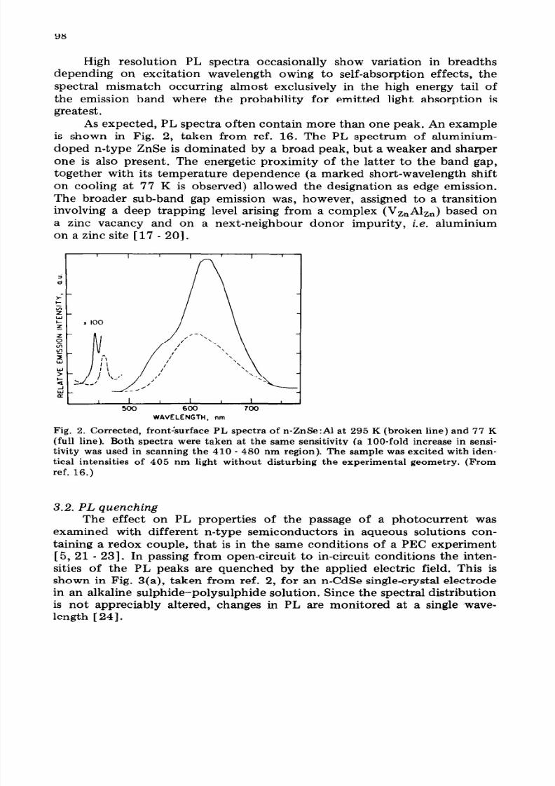
greatest.As expected, PL spectra often contain more than one peak. An example
is shown in Fig. 2, taken from ref. 16. The PL spectrum of aluminium-
doped n-type ZnSe is dominated by a broad peak, but a weaker and sharper
one is also present. The energetic proximity of the latter to the band gap,
together with its temperature dependence (a marked short-wavelength shift
on cooling at 77 K is observed) allowed the designation as edge emission.
The broader sub-band gap emission was, however, assigned to a transition
involving a deep trapping level arising from a complex (VznAlzn) based on
a zinc vacancy and on a next-neighbour donor impurity, i.e. aluminium
on a zinc site [ 17 - 201.
I L 1 I
500 600 700
WAVELENGTH. nm
Fig. 2. Corrected, front&-face PL spectra of n-ZnSe:Al at 295 K (broken line) and 77 K(full line). Both spectra were taken at the same sensitivity (a loo-fold increase in sensi-
tivity was used in scanning the 410 - 480 nm region). The sample was excited with iden-
tical intensities of 405 nm light without disturbing the experimental geometry. (Fromref. 16.)
3.2. PL quenching
The effect on PL properties of the passage of a photocurrent was
examined with different n-type semiconductors in aqueous solutions con-
taining a redox couple, that is in the same conditions of a PEC experiment
[ 5, 21 - 231. In passing from open-circuit to in-circuit conditions the inten-
sities of the PL peaks are quenched by the applied electric field. This is
shown in Fig. 3(a), taken from ref. 2, for an n-CdSe single-crystal electrode
in an alkaline sulphide-polysulphide solution. Since the spectral distribution
is not appreciably altered, changes in PL are monitored at a single wave-
length [ 241.

8/8/2019 A Review on Photo Luminescence And
http://slidepdf.com/reader/full/a-review-on-photo-luminescence-and 7/13
99
I I
650 700 750 801
(a) WAVELENGTH, nm
J
260 -
::
150- 514.5 nm EXCITATION -.
f40 -
5;;30 -
s .
320 -
5 .
FlO -
4 .
z o-
(C)r:::::‘::;::::’
-1.5 -1.3 -1.1 -0.9 -0.7 -0.5 -0.3
@IPOTENTIAL, VOLTS vs. SCE
Fig. 3. (a) Uncorrected PL spectrum of an n-CdSe single-crystal electrode excited with514.5 nm light in a 1 M OH--l M S2--0.5 M S electrolyte. Curves A, B and C were taken
at -1.50 V (open circuit), -1.45 V and -1.30 V us. SCE, respectively; all spectra wereobtained with an identical sample geometry. Photocurrent (b) and emission intensity (c)monitored at &,a, _ 720 nm us. potential for an n-CdSe single-crystal electrode excitedat 514.5 nm in a 5 M OH--O.11 M Se2--0.004 M Se 22- electrolyte. The photocurrent
quantum efficiency, f#~,, at -0.3 V (SCE) was measured and found to be about 0.9.
Related experiments with n-CdSe electrodes are given in ref. 6. (From ref. 2.)
Simultaneous measurements of photocurrent and PL intensity as a
function of electrode potential allow one to obtain the so-called ILV curves
reported in Figs. 3(b) and 3(c). There is a typical inverse correlation betweenphotocurrent and PL intensity, as the former increases the latter decreaseswhen increasingly anodic potentials are scanned. In fact, as more anodicpotentials are applied to the semiconductor, downward band bending inthe space-charge region is increased. Therefore, electron-hole separation ispromoted and radiative electron-hole recombination inhibited. Conse-quently, the photocurrent is enhanced and photoluminescent intensitydiminis)led.
Quenching of semiconductor PL by applied electric fields has been
quantified by a dead-layer model [ 25 - 271 which has recently been foundto be applicable also to PEC-based systems [ 2, 5, 16, 28 - 301. In its simplestform, the model states that electron-hole pairs formed within some fractionof the depletion width are swept apart by the field and do not contributeto PL.

8/8/2019 A Review on Photo Luminescence And
http://slidepdf.com/reader/full/a-review-on-photo-luminescence-and 8/13
100
3.3. EL spectral distribution
In Fig. l(b), taken from ref. 5, EL spectra of n-type CdS,Sei_, single
crystals in a 5 M OH--O.1 M S,Os 2- electrolyte are reported. The electrodes
were continuously pulsed between 0 and -1.5 V (SCE), thus avoiding EL
intensity decay.Another example is shown in Fig. 4, taken from ref. 15, where the
relationship between the EL spectrum and the oxidized component of the
redox couple in the electrolyte is considered. For n-GaAs, both edge (at
0.87 ,um) and sub-band gap (at 1.1 pm) emissions are observed. The latter
is related to a deep acceptor level due to gallium vacancies. The remarkable
difference between EL intensity of Ce4+- or Fe3+-containing solutions has
been explained on the basis of the higher redox potential of the Ce3+/Ce4+
redox couple assuring a better overlapping of the electrolyte empty energy
levels and both the valence band and the deep acceptor level. Therefore,
Ce4+ ions easily inject holes into the semiconductor, whereas Fe3+ ions
do not [ 151.
EL spectra are typically recorded under conditions which facilitate
comparisons with PL spectra. As Figs. l(a) and l(b) clearly show, there is
a striking similarity between the PL and the EL spectra, thus indicating
that an identical emissive excited state is involved in both experiments.
In other cases, however, particularly when a high resolution is em-
ployed, spectral differences in the high energy tail of EL and PL spectra
are observed [ 5, 6, 151. This spectral mismatch has been attributed to
greater self-absorption of the emitted light in the PL experiment [ 5, 61.
WAVELENGTH (pm)
Fig. 4. Uncorrected EL spectra of n-GaAs in 0.01 M Fe,(SO& + 1.0 M HzS04 and in0.03 M Ce(SO& + 1.0 M HzSO 4. The electrode potential was continuously pulsed be-
tween 0 (20 s) and -1.75 V (2 s), while the emission spectrum was scanned at 5 w 6-l.
Note the tenfold increase in sensitivity in order to record the spectrum in the Fe,(SO&
electrolyte. (From ref. 15.)

8/8/2019 A Review on Photo Luminescence And
http://slidepdf.com/reader/full/a-review-on-photo-luminescence-and 9/13
101
As on average EL is significantly more surface sensitive than PL,
several semiconductors show some EL emission peaks below the band-gapenergy which do not appear in the PL spectrum (compare curves a and c ofFig. 5, taken from ref. 31). It has been suggested that these additional peaks
originate from transitions involving hole-accepting, i.e. filled, surface states[4, 5, 7, 9, 31, 321.
The rather exceptional case of a PL peak having no EL counterpart(compare curve c with curve b of Fig. 5) indicates that the empty en-ergy levels of the redox couple in the electrolyte (i.e. the energy levels of
Fe(CN),3-) and the valence band do not overlap. However, such emptylevels overlap the hole-accepting surface states and, therefore, can directlyinject holes into them, thus producing the EL peak around 900 nm shownin curve b of Fig. 5 [31].
1 0 0 0 800 600 (nm)
Fig. 5. CdS PL and EL spectra in the following electrolytes: curve a, EL in i M KOH-0.1
M KzSzOs; curve b, EL in 1 M KOH-0.1 M K3Fe(CN)s; curve c, PL in 0.2 M NazS03-0.2
M NazS04. (From ref. 31.)
3.4. Efficiencies
3.4.1. PL efficiencyThe quantum efficiency of PL q& (defined as photons emitted per
photon absorbed (or per populated excited state)) is very difficult toestimate with accuracy. Therefore, an upper limit can be obtained by findingother experimental conditions (e.g. cooling the material) which markedlyenhance the emission [ 61. Another technique developed by Wrighton et al.
[33] compares light reflected from a non-absorbing material with lightreflected and emitted from the sample.
Sometimes, 4, was observed to decrease with the excitation wavelengthand such behaviour has been attributed to the presence of a near-surfacenon-emissive region which absorbs larger fractions of incident light, thusreducing 9, [ 161.
By considering the different excited-state decay routes, one mayobtain a very simple relationship that connects 4, with the photocurrent
8/8/2019 A Review on Photo Luminescence And
http://slidepdf.com/reader/full/a-review-on-photo-luminescence-and 10/13
102
quantum efficiency 4, defined as electrons circulating in the external circuit
of the PEC cell per absorbed photon.
Assuming that the only decay routes of the photoproduced electron-
hole pairs are radiative emission (PL), photocurrent and non-radiative
emission, whose quantum efficiencies are $,, 4, and @,,, respectively, 4, +@J,+ @Xl, 1 [ W.
For a cell operating in open-circuit conditions
whereas, when operating in in-circuit conditions
~, = Eli and ~, = ~xi,
hence [22, 341
4
z=1
’ - @Xi
provided the ratio &/#,, of the electron-hole pairs radiatively recombining
to those non-radiatively recombining is unaffected by potential.
The above equation allows the calculation of the degree of PL quench-
ing by potential, but discrepancies from the theoretical predictions have
been observed [ 221. It also allows determination of the & value which may
be compared with the experimental value from PEC measurements. Rea-
sonable agreement was obtained for PEC cells based on n-CdS,Se, - X (0 S
x < 1) and on Te-doped n-CdS [5,22,34,35].
3.4.2. EL efficiency
EL efficiency can be determined in both steady state and pulse experi-
ments. In the first case, the instantaneous efficiency $xL is obtained (photon
emitted per hole injected), in the second case, the integrated efficiency 4xL
(total photons emitted per total holes injected). The measurements are
performed by placing a radiometer next to the emitting surface. Since not
all of the emitted photons are collected, EL efficiencies are lower-limit
estimates [ 351.Taking the definition of EL and PL efficiencies into account, it is
possible to factor I& into 4, (photons emitted per populated excited state)
and $xS (efficiency for excited-state population, i.e. populated excited states
per holes injected) [ 161:
However, conclusions regarding r$Es based on the direct comparison
of EL and PL efficiencies must be drawn carefully. In many systems (e.g.
n-CdSe [6] and n-CdS,Se, _-x [5]) @Es is large, approaching its maximum
value of unity. However, in other cases (e.g. Al-doped n-ZnSe [16]), since
@EL g 4,) @ES is very small, but more likely this reflects the different spatial
origin of EL and PL. Moreover, reduction of the electrode surface during EL
experiments may also contribute to the above discrepancy [ 51.

8/8/2019 A Review on Photo Luminescence And
http://slidepdf.com/reader/full/a-review-on-photo-luminescence-and 11/13
103
4. Concluding remarks
PL and EL provide a sensitive in situ tool for the characterization of
deep level traps in semiconductors and of intra-band gap states at the semi-
conductor-electrolyte interface, respectively. Moreover, since PL and ELspectra are typical for each semiconducting compound and since by changing
the wavelength of the exciting light it is possible to vary the light penetration
depth, PL and EL also allow one to monitor chemical and electronic changes
occurring in the region close to the interface.
Therefore, in performing PL and EL measurements, it is imperative
to control the electrode potential to avoid too drastic chemical changes at
the semiconductor interface.
Regarding this point, Etcheberry et al. [30] carried out a PL study on
the compositional changes of an n-InP surface in a pH 1 solution of perchlo-
ric acid by polarizing the electrode at more positive and more negative
potentials than the rest potential. From the shape of the PL intensity uersus
potential curve, they concluded that the electrode surface (like that of Ge
and GaAs [ 361) evolves from a stable oxidized state (i.e. oxygen covered)
to a reduced one (i.e. mainly hydrogen covered) when the bias is changed
from positive to negative. In the latter case, adsorbed species which appear
during hydrogen evolution, e.g. atomic hydrogen, are able to enhance PL.
They are assumed to passivate surface defects, thus diminishing non-radiative
recombination.
Electrode potential control is particularly stringent for EL experimentswhere the semiconductor has to be cathodically polarized in order to achieve
light emission.
Therefore, Gerischer et al. [37] have recently questioned whether
observed dissimilarities between PL and EL spectra are “caused by the dif-
ferent distribution of minority carriers in the two experiments or by chemi-
cal changes, at the semiconductor-electrolyte interface, as a direct result
of the different techniques”.
Taking the potentialities of PL and EL techniques into account, several
problems connected with semiconductor surfaces have been studied. Somesignificant examples will suffice to illustrate the situation.
Surface adsorption phenomena resulting from the interaction between
a semiconductor and a solution were investigated. PL intensity of n-InP was
found to decrease as soon as the semiconductor was immersed in an aqueous
electrolyte mainly as a consequence of adsorption of ionic or dipolar species
belonging to the solution [ 301.
Other examples are surface modification due to corrosion and aging
both in the dark and under illumination of photoelectrodes in liquid junc-
tion configuration. Recently, the evolution of the PL spectrum of n-CdSe
in sulphide-polysulphide solutions has been monitored as a function oftime and light intensity in order to elucidate the aging process mechanism
of one of the most promising materials for regenerative PEC cells [38]. The
predominant aging process which occurred under open-circuit conditions
8/8/2019 A Review on Photo Luminescence And
http://slidepdf.com/reader/full/a-review-on-photo-luminescence-and 12/13
104
was well correlated with the formation of an insulating CdS,Se,_, film atthe surface. By penetrating deeper into the electrode, the mixed compoundseparated into CdS and CdS,Se, _ Y which was considerably poorer in sul-phur [38].
Surface modifications due to treatments such as etching, PEC etchingas well as adsorption of metal ions to which semiconductors are submittedin order to increase their PEC behaviour have also been examined through
their effect on luminescence properties [ 391.Although surface treatments obviously affect EL spectra more than PL
spectra, evidence was found that PL and its spatial distribution may beinfluenced, too.
Both etching and photoetching of CdSe electrodes resulted in anincrease in the emitted light (up to 50 times after photoetching) and in abroadening of the high energy portion of the emission band [6]. Such an
enhancement of PL intensity suggested a substantial increase in PL efficiencyand the concomitant spectral mismatch indicated a greater contribution toPL from regions on average nearer the semiconductor-electrolyte interface.At present, there are uncertainties as to the origin of these effects and
research is still in progress [ 61.It may thus be concluded that PL and EL spectroscopies are very
important tools for surface properties investigation, as even these few
examples have shown. Therefore, it is very easy to predict an increasingdevelopment of these techniques in the near future.
References
1 L. Peraldo Bicell i, Surf. Technol., 20 (1983) 357.
2 A. B. Ellis, J. Chem. Ed., 60 (1983) 332.
3 R. E. Halsted, in M. Aven and J. S. Prener (eds.), Physics and Chemistry of II-VI
Compounds, North-Holland, Amsterdam, 1967, Chap. 8.
4 H. H. Streckert, B. R. Karas, D. J. Moran0 and A. B. Ellis, J. Phys. Chem., 84 (1980)3232.
5 H. H. Streckert, J. Tong, M. K. Carpenter and A. B. Ellis, J. Electrochem. Sot., 129
(1982) 772.6 H. H. Streckert, J. Tong and A. B. Ellis, J. Am. Chem. Sot., 104 (1982) 581.7 K. H. Beckmann and R. Memming, J. Electrochem. Sot., 116 (1969) 368.
R. Memming, J. Electrochem. Sot., 116 (1969) 785.
8 F.-R. F. Fan, P. Leempoel and A. J. Bard, J. Electrochem. Sot., 130 (1983) 1866.9 B. Pettinger, H. R. S chijppel and H. Gerischer, Ber. Bunsenges. Phys. Chem., 80
(1976) 849.10 D. M. Kolb and H. Gerischer, Electrochim. Acta, 18 (1973) 987.11 H. Masuda, A. Fujishima and K. Honda, Chem. Lett., (1980) 1153.12 Y. Nakato, A. Tsumura and H. Tsubomura, in A. J. Nozik (ed.), Photoeffects at
Semiconductor-Electrolyte Interfaces, ACS Symp. Ser., American Chemical Society,
Washington, DC, 1981, p. 145.13 S. Menezes and B. Miller, J. Electrochem. Sot., 130 (1983) 517.
14 F. Decker, B. Pettinger and H. Gerischer, J . Electrochem. Sot., 130 (1983) 1335.
15 F. Decker, M. Abramovich and P. Motisuke, J. Electrochem. Sot., 131 (1984) 1173.
16 P. M. Smiley, R. N. Biagioni and A. B. Ellis, J. Electrochem. Sot., 131 (1984) 1068.

8/8/2019 A Review on Photo Luminescence And
http://slidepdf.com/reader/full/a-review-on-photo-luminescence-and 13/13
105
17 D. Curie and J. S. Prener, in M. Aven and J. S. Prener (eds.), Physics and Chemistry
ofZZ-VI Compounds, North-Holland, Amsterdam, 1967, Chap. 9.4.
18 S. Iida, J. Phy s. Sot . Jpn., 25 (1968) 177.
19 G. Jones and J. Woods, J. Lumin., 9 (1974) 389.
20 S. Satoh and K. Igaki, Jpn. J. Appl. Phys., 22 (1983) 68.
21 G. Petermann, H. Tributsch and R. Bogomolni, J. Chem. Phys., 57 (1972) 1026.22 A. B. Ellis, B. R. Karas and H. H. Streckert, J. Chem. Sot., Faraday Discuss., 70
(1980) 165.
23 A. Fujishima, Y. Maeda, S. Suzuki and K. Honda, Chem. Lett., (1982) 179.
24 B. R. Karas and A. B. Ellis, J. Am. Chem. Sot., 102 (1980) 968.
25 K. Ando, A. Yamamoto and M. Yamaguchi, J. Appl. Phys., 51 (1980) 6432.
26 K. Ando, A. Yamamoto and M. Yamaguchi, Jpn. J. Appl . Phy s., 20 (1981) 679.
27 R. E. HoIIingsworth and J. R. Sites, J. Appl. Phys., 53 (1982) 5357.
28 W. S. Hobson and A. B. Ellis, J. Appl. Phys., 54 (1983) 5956.
29 R. Garuthara, M. Tomkiewicz and R. P. Silberstein, J. Appl. Phys., 54 (1983) 6787.
30 A. Etcheberry, J. Gautron, R. Parsons and J. L. Sculfort, 35th Meeting of Znt erna-
tional Societ y of Electrochemist ry, Berkeley, CA, August 5 - 10, 1984, AnstractA3-31.
31 I. Jimenez, F. Decker and P. Salvador, 35th Meeting of International Society of
Electrochemist ry, Berkeley, CA, August 5 - 10, 1984, Abstract 112-3.
32 Y. Nakato, A. Tsumura and H. Tsubomura, Chem. Phys . Lett ., 85 (1982) 387.
33 M. S. Wrighton, D. S. Ginley and D. I. Morse, J. Phy s. Chem., 78 (1974) 2229.
34 B. R. Karas, D. J. Morano, D. K. Bilich and A. B. Ellis, J. Electrochem. Sot ., 127
(1980) 1144.
35 B. R. Karas, H. H. Streckert, R. Schreiner and A. B. Ellis, J. Am. Chem. Sot., IO3
(1981) 1648.
36 H. Gerischer and I. Mattes, 2. Phys. Chem. N.F., 49 (1966) 112.
37 H. Gerischer, R. McIntyre and B. Smandek, 35th Meeting of International Society
of Electrochemist ry, Berkeley, CA, August 5 - 10, 1984, Abstract A3-1.
38 M. Tomkiewicz and R. Garuthara, 35th M eeting of International Society of Electro-
chemistry , Berkeley, CA, August 5 - 10, 1984, Abstract A3-2, in J. Appl. Phys., 58
(1985) 1662.
39 N. Miiller, M. Abramovich, F. Decker, F. Iikawa and P. Motisuke, J. Electrochem.
Sot., 131 (1984) 2204.