a review of graphene plasmons and its combination with ... · pdf filethe current challenges...
TRANSCRIPT

Journal of the Korean Ceramic Society Vol. 54, No. 5, pp. 349~365, 2017.
− 349 −
https://doi.org/10.4191/kcers.2017.54.5.10
†Corresponding author : Yang Bai E-mail : [email protected] Tel : +86-10-6233-4493 Fax : +86-10-6233-4493
A Review of Graphene Plasmons and its Combination with Metasurface
Chuanbao Liu*, Yang Bai*,†, Ji Zhou**, Qian Zhao***, and Lijie Qiao*
*Key Laboratory of Environmental Fracture (Ministry of Education), University of Science and Technology Beijing, Beijing 100083, China
**State Key Laboratory of New Ceramics and Fine Processing, Tsinghua University, Beijing 100084, China***State Kay Laboratory of Tribology, Department of Mechanical Engineering, Tsinghua University, Beijing 100084, China
(Received July 23, 2017; Revised September 5, 2017; Accepted September 6, 2017)
ABSTRACT
Graphene has attracted a lot of attentions due to the unique electrical and optical properties. Compared with the noble metal
plasmons in the visible and near-infrared frequencies, graphene can support surface plasmons in the lower frequencies of tera-
hertz and mid-infrared and it demonstrates an extremely large confinement at the surface because of the particular electronic
band structures. Especially, the surface conductivity of graphene can be tuned by either chemical doping or electrostatic gating.
These features make graphene a promising candidate for plasmonics, biosensing and transformation optics. Furthermore, the
combination of graphene and metasurfaces presents a powerful tunability for exotic electromagnetic properties, where the meta-
surfaces with the highly-localized fields offer a platform to enhance the interaction between the incident light and graphene and
facilitate a deep modulation. In this paper, we provide an overview of the key properties of graphene, such as the surface con-
ductivity, the propagating surface plasmon polaritons, and the localized surface plasmons, and the hybrid graphene/metasur-
faces, either metallic and dielectric metasurfaces, from terahertz to near-infrared frequencies. Finally, there is a discussion for
the current challenges and future goals.
Key words : Electrical properties, Optical properties, Sensors
1. Introduction
raphene, a single layer of carbon atoms arranged in
honeycomb structures, has attracted extensive atten-
tions since the advent of free-standing graphene sheets in
2004.1) Because of the linear dispersion relation of Dirac
electronic states, graphene demonstrates the unique electri-
cal and optical properties,2,3) such as high carrier mobility,
broadband operation, and a tunable band gap, which make
it a fantastic material for photonics and optoelectronics.4-6)
The optical response of graphene can be described by the
surface conductivity which is originated from the contribu-
tions of inter-band and intra-band transitions, related to the
chemical potential or Fermi level.7,8) In the near-infrared
and visible frequencies, the graphene manifests a strong
absorption caused by the inter-band transitions.7,9) In the
terahertz and mid-infrared frequencies, the graphene
behaves as an ultrathin metal film, supporting the surface
plasmon polaritons (SPPs) with the greatly enhanced local
fields at the graphene surface.10-13) Compared with the con-
ventional metal palsmons primarily working in the visible
frequencies, the SPPs in graphene demonstrate a stronger
confinement and lower loss, that is, an extremely short
wavelength and a long propagation distance.12) Most import-
ant, SPPs in graphene can be dynamically tuned by the
chemical doping14) or electrostatic gating.15) As a result,
graphene has promising applications for high performance
SPP-based nano-devices.16)
Due to the large mismatch between the wave vector of
SPPs and the incident light, many methods, such as nano-
emitters/tips scattering,12,13,17-23) gratings24-27) and prism cou-
pling,28,29) have been proposed. However, the coupling effi-
ciency in the above methods is very low. Alternatively, the
structured graphene (sub-wavelength nanoparticles) can
demonstrate localized surface plasmons (LSPs) resonance
with a strongly confined local field at the surface of nano-
particles.30-37) Compared with the propagating SPPs, LSPs
resonance is a non-propagating regime and can be directly
excited by a light with appropriate polarization and fre-
quency. Apart from the strong light-matter interaction for
sensing applications, the structured graphene is capable of
modulating phase and amplitude used in polarization con-
verter,38,39) optical activity40) and wavefront reshaping appli-
cations.41-44)
The optical response for the monolayer graphene usually
has a limited modulation depth due to the fact of single
atomic thickness. To obtain a more powerful capacity of
modulation, the hybrid graphene/metasurfaces have been
proposed as a possible solution.45-48) Metasurfaces are com-
posed of sub-wavelength scatters which can interact with
the electric or magnetic field components of incident light to
produce the desired responses, including the phase shift,
G
Review

350 Journal of the Korean Ceramic Society - Chuanbao Liu et al. Vol. 54, No. 5
amplitude and polarization. By arranging the spatial distri-
bution of the designed scatters treated as the tiny secondary
sources, the metasurface can arbitrarily manipulate the
electromagnetic wavefront, leading to myriad applications,
such as holograms,49-51) meta-lens52-55) and abnormal refrac-
tion.56-58) Compared with the conventional optical compo-
nents or bulky metamaterials59,60) depending on the electro-
magnetic wave propagating in the bulky media to gradually
accumulate the changes of wavefront, the metasurfaces can
realize the abrupt changes in a sub-wavelength-thin thick-
ness, endowing the superior advantages of miniaturization,
lightening and thinning. A drawback of conventional meta-
surfaces is non-tunability after they were fabricated. The
versatile functionality of metasurfaces depends on the unit
cells which are implemented by metallic patterns or dielec-
tric cubes based on the plasmonic or Mie resonances.56,61-63)
It opens up an avenue to dynamically control light when the
active graphene integrates with metasurfaces, which de-
monstrates more extensive application prospects, such as
fast optical modulators,46,64-67) switches45,47) and other optical
devices.68,69) In addition, graphene is compatible with the
nanofabrication technology and easy to be integrated into
the nano/micro-sized metasurfaces.
This paper is organized as described below. In section 2,
we overview the surface conductivity of graphene from tera-
hertz to visible frequencies by the random-phase approxi-
mation (RPA) theory. In section 3, we introduce the pro-
pagating SPPs in graphene, including the characteristics,
SPPs excitation, and SPPs hybridization. In section 4, we
introduce LSPs in the structured graphene, modulation
depth of absorption and electromagnetic applications, such
as polarizer and meta-lens. In section 5, we overview the
hybrid graphene/metallic metasurface working from tera-
hertz to near-infrared frequencies, and the hybrid graphene/
dielectric metasurface mainly working in the near-infrared
frequencies. In the last section, we provide some concluding
remarks and present an outlook on future research direc-
tions.
2. Surface Conductivity of Graphene
2.1. Surface conductivity at terahertz and infrared
frequencies
The optical response of graphene is derived from the
dynamic surface conductivity closely related to chemical
potential or Fermi level. It can be derived with the random-
phase approximation (RPA) theory8) and originate from the
contribution of intra-band and inter-band transitions as
below,
(1)
where e is the electron charge, kB is the Boltzmann’s con-
stant, ћ is the reduced Planck’s constant, T is the tempera-
ture, and ω is the angular frequency of incident light. τ is
the relaxation time and estimated by expression ,
where vf = 106 m/s is the Fermi velocity, u is the carrier
mobility of graphene and ranges from 1000 cm2/Vs in chem-
ical vapor deposition (CVD)70,71) to 100 m2/Vs in suspended
graphene.72) EF is the Fermi level which translates to the
carrier concentration of . In most cases, the
Fermi energy EF is limited range of −1.0 eV to 1.0 eV as the
consideration of device requirements to guarantee against
the breakdown electric field of the gate dielectric.73) The first
and second terms are attributed to the intra- and inter-band
transitions, respectively.
Figure 1 is the calculated results based on Eq. (1). In the
terahertz and mid-infrared frequencies where the photonic
energy is far below the double Fermi level ( ),
the surface conductivity of graphene are dominated by the
intra-band transitions (Fig. 1(a)). The inter-band transi-
tions are diminished due to the presence of electrons and
holes near the band edges (Pauli blocking). The surface con-
ductivity can be reduced to
σs ω( ) = i 2e
2kBT⋅
πh2
ω iτ1–
+( )-------------------------------ln 2cosh
EF
2kBT--------------⎝ ⎠
⎛ ⎞
+ e
2
4h-------
12---
1π--- arctan
hω EF–
2kBT-------------------⎝ ⎠
⎛ ⎞ i2π------ln
hω+EF( )2
hω EF–( )2
2kBT( )2+
---------------------------------------------------–+ +
τ = uEF/evf2
n = EF2/πh
2vf
2
hω << 2 EF
Fig. 1. (a) Real parts of intra-band (solid) and inter-band (dash) surface conductivities of graphene with EF = 0.2 eV (black) andEF = 0.4 eV (red). The carrier mobility is assumed to be µ = 1000 cm2/Vs. The inset shows the band structure of graphene.(b) The optical response of moderately doped graphene in different spectral ranges. In the terahertz, near-infrared or mid-infrared frequencies, graphene exhibits a lossy (|Im(σs)/Re(σs) < 1|) or plasmonic behavior (Im(σs)/Re(σs) > 1), respec-tively.

September 2017 A Review of Graphene Plasmons and its Combination with Metasurface 351
. (2)
When the Fermi level is , the surface conduc-
tivity is further simplified to
. (3)
From Eqs. (2) and (3), the graphene just behaves as a con-
ductive film and can be described by a classical Drude
model. As a result, the graphene can support the transverse
magnetic (TM) polarized SPPs. The surface conductivity
presents a linear relationship with the Fermi level EF. Note
that a considerable loss caused by the intra-band transi-
tions is inevitable in the terahertz frequencies (Fig. 1(b))
which can be utilized to modulate amplitude by the absorp-
tion in graphene instead.
However, in the mid-infrared frequencies, the surface con-
ductivity approaches the minimum due to the Pauli block-
ing and a relatively large incident frequency, degenerating
the inter-band and intra-band transitions (Fig. 1(a)). The
imaginary part of conductivity becomes dominant over the
real part, facilitating to support the transverse magnetic
SPPs with an extremely low loss (Fig. 1(b)). In the terahertz
and mid-infrared frequencies, the conductivity of graphene
has a largely tunable range which is facilitated to large-
scalely tune the amplitude or frequency of the plasmon reso-
nance when the graphene critically couples with the meta-
surface of enhanced local field. Besides, the very thin
“metal” layer can be further tailored to different shapes to
obtain the desired resonances and reshape wavefront.
For the numerical simulations, graphene is often modeled
as an anisotropic medium with in-plane effective permittiv-
ity as
(4)
where ε0 is the vacuum permittivity, tg is the thickness of
graphene, is the plasm
frequency. The out-plane effective permittivity is equal to
the vacuum permittivity of εeff,n = 1.0.
2.2. Surface conductivity at near-infrared and visi-
ble frequencies
On the contrary, the inter-band transitions become a deci-
sive factor ( ) in the near-infrared and frequen-
cies, as shown in Fig. 1(a). The free carrier scattering rate
τ −1 can be treated as zero due to the small quantity com-
pared with the incident frequency.74) The real part of the
surface conductivity is changed from 0 to e2/4ћ (universal
optical conductivity) by electrically tuning Fermi level,
which results in a modulation of absorption from 0 to 2.3%
under the normal incidence. Obviously, the limited range of
surface conductivity also limits the modulation depth of an
isolated graphene, no matter for the transmission, reflection
and absorption.75) To get a large modulation, the metasur-
face which can capture light from free space and offer a local
filed enhancement in plane (two to three orders of magni-
tude larger than the incident field) is critical coupling with
the tunable graphene. Besides, the imaginary part of the
graphene permittivity becomes dominant over the real part
so that the surface plasmons cannot be sustained at the
graphene surface.10) In the visible frequencies, graphene can
be visualized despite of only a single atom thick, due to a
significant absorption πα = 2.3%, where α = 1/137 is the fine
structure constant that describes coupling between light
and electrons.
It is noted that the surface conductivity can also be tuned
by the photonic excitation,76) magnetic field77) and strain
mechanism,78) in addition to the common electrostatic gat-
ing and chemical doping.
3. Propagating Surface Plasmon Polaritons in Graphene
3.1. Properties of SPPs
The SPP is a collective oscillation of conduction electrons
or holes along the boundary surface of a metal or semicon-
ductor under the drive of electric field component of an inci-
dent light. It can highly confine the plasmonic wave and
strongly enhance the electric field in the vicinity of surface,
promising applications for the light-mater interactions,
such as chemical, biological sensing and surface-enhanced
Raman scattering.79) As stated above, the graphene behaves
as a metal film in the terahertz and infrared frequencies,
i.e. it is capable of supporting transverse magnetic polarized
SPPs. For the simplest dielectric/continuous graphene sheet
(the size larger than SPPs wavelength)/dielectric prototype,
the dispersion relationship of SPPs is given by10,80)
, (5)
where β is the wave-vector of SPPs in graphene, εr1 and εr2
are the permittivity of dielectric above and below the
graphene. Note that the precondition for the establishment
of Eq. (5) is k0 << β << kF (in non-retarded regime and long
wavelength limit), where k0 and kF are the vacuum and
Fermi wave-vectors. For a finite β compared with kF, the
dispersion of SPPs will deviate the Eq. (5) and present a lin-
ear relationship or damping regime.81) In addition, the dis-
persion of SPPs is also influenced by the polar medium,
where the surface optical phonons couple with the SPPs via
a long-range Fröhlich coupling.82)
Compared with the conventional noble metal (silver and
gold) plasmons, the graphene supported SPPs have many
prominent properties. (1) Huge modal index or extensive
confinement. For clarity, the Eq. (5) is simplified to
, (6)
σs ω( ) = i 2e
2kBT⋅
πh2
ω iτ1–
+( )-------------------------------ln 2cosh
EF
2kBT--------------⎝ ⎠
⎛ ⎞
EF >> kBT
σs ω( ) = i e
2EF⋅
πh2
ω iτ1–
+( )-------------------------------
εeff,t = 1iσs
ε0ωtg-------------+ = 1
ωp2
ω2
------–
ωp = (2e
2kBT
πh2ε0tg
--------------------ln[2cosh(EF
2kBT---------------)])
1/2
hω > 2 EF
β ω( ) = i εr1 εr2+( )ε0ω
σs ω( )---------------------------------- =
πh2ε0 εr1 εr2+( )
e2EF
-------------------------------------ω ω iτ1–
+( )
β ω( )εr1 εr2+( )hω
4αEF
------------------------------k0≈

352 Journal of the Korean Ceramic Society - Chuanbao Liu et al. Vol. 54, No. 5
where the scattering rate is assumed to zero, α = e2/
4πћε0c = 1/137 is the fine structure constant, the weight of
is order of 1. Hence, the wave-vector of SPPs in
graphene is two orders of magnitude bigger than the vac-
uum wave-vector.13,19,20) The wave-vector of SPPs in the
noble metal, by contrast, is slightly larger than the vacuum
wave-vector.83) (2) Relatively low losses or longer propaga-
tion. In the mid-infrared frequencies, the surface conductiv-
ity reaches the minimum, as shown in Fig. 1. The real part
of permittivity in the graphene dominate the imaginary
part, resulting in a relatively low damping loss of SPPs and
a longer propagation length about hundreds of wavelength
of SPPs, comparing to a range of tens of optical cycle for
SPPs on metals. (3) Dynamic tunability. From Eq. (5), the
propagation of SPPs in graphene is related to the Fermi
level which can be tuned by electric field, magnetic field,
electrostatic gating and chemical doping in real time. (4)
Broadband operation. For the SPPs at the metal/dielectric
surface which only works for the frequencies close to the
plasma frequency of metal. At terahertz and infrared fre-
quencies, the metal behaves as a perfect conductor with
delocalized SPPs. On the contrary, the SPPs can be sup-
ported by the graphene from terahertz to near-infrared fre-
quencies by controlling the Fermi level. These unique
features make the graphene a promising platform for the
active SPP-based nano-optoelectronic devices, plasmonics
and transformation optical devices by spatially varying the
graphene Fermi level in the terahertz and infrared frequen-
cies.84)
3.2. SPPs excitation
The major challenge is to efficiently excite SPPs in
graphene with a free space incident light due to the large
wave-vector mismatch between two waves. Conventional
plasmonics approaches, such as the diffractive grating,24-27)
shifts the wave-vector of the incident light to compensate
the mismatch due to Bragg scattering following the expres-
sion of β = sinθk0 + 2nπ/Λ, where n is the diffraction order, Λis the periodicity, θ is the incident angle. Fig. 2(a) and (b)
show the silicon-diffractive grating-assisted graphene plas-
mon excitation by guided-wave resonance.24) The Fourier
transform infrared spectroscopy (FTIR) measurement
result of T+/T//, where T+ and T// are the transmission spec-
trum under the normal incidence polarized perpendicular
and parallel to the gratings lines, demonstrates a resonant
dip due to the absorption of SPPs in the graphene (Fig. 2(c)).
It is noted that, to efficiently excite the SPPs, a large cou-
pling length is required (in the order of incident wave-
length), which goes against the compactness of the nano-
devices and bring a challenge to the nanofabrication.
Another conventional method to excite the SPPs is using
the prism coupling,28,29) such as the Otto or Kretschmann
configurations,85,86) where the evanescent wave propagates
along the metal-dielectric interface, due to the total internal
reflection under the condition of the incident angle (θ)
larger than the critical angle (θc). However, the huge differ-
ence of wave-vector between the evanescent wave and the
incident light requires a high refractive index of the prism
( ), according to the equation β = k0npsinθ, which
is not available practically. Nikitin et al.29) proposed a tact-
ful configuration (Fig. 2(d)) to excite the SPPs in graphene
based on the compression of surface polaritons (SPs) on the
tapered slabs of a polaritonic material supporting either
surface phonon polaritons (SPhPs) or SPPs, as shown in
Fig. 2(e) and (f). The SPhPs or SPPs generating by the
prism coupler propagate along the tapered slab and gradu-
τ1–
hω/EF
np 10 100–≈
Fig. 2. (a) Schematic of silicon-diffractive grating-assisted graphene plasmon excitation by guided-wave resonance (GWR). (b)Scanning electron microscopy (SEM) image of transferred graphene on a silicon grating, where the dark regions are thecracks. (c) Electrical tuning of the fabricated GWR graphene plasmonic device where arrows indicate the position of theresonant dips. (d) Schematic of the proposed coupling device, consisting of an Otto prism (couple the incident light toSPs), a tapered slab (compress the wavelength of SPs) and a thin slab (couple the SPs to SPPs in graphene). (e, f) Snap-shots of the real part of the vertical component of the electric field Re(Ez) for SiC and n-GaAs waveguides. (a) - (f) usedwith permission from24,29) copyright by 2013, 2014 by American Chemical Society.

September 2017 A Review of Graphene Plasmons and its Combination with Metasurface 353
ally yield a compression of wavelength to match the SPPs in
graphene finally.
Besides the above methods, the excitation of SPPs is also
proposed by coupling the near field of the nano-emitters
with graphene.12,13,17-23) Typically, the metallized tip of an
atomic force microscope (AFM) illuminated by a focused
infrared laser beam generates strong evanescent electric
fields with a wide range of in-plane momenta which can
effectively excite the graphene plasmons. In combination
with the scattering-type scanning near-field optical micros-
copy (s-SNOM),13,19,20,23) the SPPs reflected or scattered by
the external and internal edges, atomic defects, and bound-
aries of single-layer or multilayer graphene are visualized
including amplitude and phase. Fig. 3(a) shows the illustra-
tion of the tip-induced SPPs excitation.20) Under the illumi-
nation of a CO2 laser with a wavelength of λ = 10.8 μm, the
s-SNOM amplitude and phase exhibits the standing waves
for SPPs due to the existence of external (transition from
single and bilayer graphene) and internal (folds and grain
boundaries) defects. The SPPs wavelength (λspp) in single
and bilayer graphene are (260 ± 10) nm and (190 ± 10) nm,
with a reflection coefficient of , respectively (Fig.
3(b)). The SPPs in both sides of the line defects have differ-
ent wavelength of 240 nm and 260 nm, as well as different
reflection coefficients of and 0.55 (Fig. 3(c)). The
ratio of λspp/λ0 is in the order of the fine structure constant.
Besides, the change of Fermi level can effectively tune the
SPPs wavelength. The full amplitude and phase spatially
resolved imaging provides nano-scale insight into the local
electronic structure and dynamics in graphene.
Figure 3(d) demonstrates the propagating SPPs in
graphene excited by the dipole nano-antenna under the inci-
dent light (λ0 = 10.20 μm or 11.06 μm) polarized parallel to
the long axis and imaged by s-SNOM with a dielectric Si-tip
which passively scatter the near field of the graphene plas-
mon and gather the cross-polarization with a polarizer in
front of the detector.87) The study shows the efficiency of res-
onance is enhanced by a factor of 28 compared with the non-
resonant antennas. Besides, the wavefront of SPPs can be
engineered by the shape of resonant antennas, such as con-
cave and convex extremities (Fig. 3(e) and (f)). Further, the
author demonstrated the propagating direction of SPPs can
be controlled by a 2D graphene bilayer prism based on the
conductivity patterns84) and revealed that the wavenumber
in graphene is also influenced by the number of graphene
layers (λspp ~ N −1/2, N is the number of layers) which qualita-
tively followed the Snell’ law (Fig. 3(g)).37)
Furthermore, the SPPs in graphene can be visualized by
the electron energy-loss (EEL) spectrum imaging22) at the
atomic scale which offers a platform to study the effect of
R̃ 1–=
R̃ 0.45=
Fig. 3. (a) Illustration of metallic tip-induced SPP excitation and subsequent interference due to the emission of scattered andreflected SPP waves. (b, c) AFM topography (left), near-field amplitude (middle), and near-field phase (right) of agraphene wedge and a region of single-layer graphene with a high concentration of grain boundaries and folds. (d) Sche-matic of an antenna-based graphene SPPs launcher. (e, f) Experimental near-field images Re(Es,p) of a convex and a con-cave antenna extremity, respectively (λ0 = 11.06 µm). (g) Experimental near-field image Re(Es,p) of a bilayer grapheneprism on a monolayer graphene (λ0 = 10.20 µm). (a) - (c) used with permission from20) copyright 2014 by American Physi-cal Society, (d) - (g) used with permission from87) copyright 2014 by AAAS.

354 Journal of the Korean Ceramic Society - Chuanbao Liu et al. Vol. 54, No. 5
single atom on monolayer graphene sheets and brings the
possibilities for designing atomic-scale optoelectronic and
plasmonic devices.
3.3. SPPs hybridization
So far, we mainly review the excitation of SPPs in mono-
layer graphene sheet with a large size compared with the
plasmon wavelength. Actually, the interaction of spatially
separated graphene sheets is also an important subfield of
graphene plasmon, because it is not only a fundamental
issue but also provides a wider range of application pros-
pects. Fig. 4(a) shows a graphene waveguide splitter.88) The
propagating SPPs in the high doped graphene ( )
are completely transferred to the adjacent graphene by the
weak SPPs coupling in the coupling region (top, Fig. 4(a)).
By decreasing the Fermi level of the graphene in the upper
or low coupling region to the condition of , where
the graphene no longer supports SPPs (middle and bottom,
Fig. 4(a)), the configuration realizes a tunable optical split-
ter or switch. Then, the author studied the strong coupling
of SPPs in the monolayer graphene sheet arrays (MGSA)
(Fig. 4(b)),89) which are physically different from the above
case with weak coupling and demonstrate interesting prop-
erties (Fig. 4(c)). Beyond that, the SPPs in the monolayer
graphene ribbon and the plasmonic hybridization of the
spatially separated graphene ribbons are also intensively
studied.90,91) The graphene ribbon supports an edge SPPs (E-
SPPs) with a strongly localized field at the ribbon edges
except the waveguide SPPs with the field concentration
within the ribbon area. Especially, the graphene ribbon
pairs demonstrate a more intensive enhancement of field.91)
Benefiting from the fascinating properties of SPPs in
graphene in the terahertz and mid-infrared frequencies, the
graphene opens up an exciting opportunity for the active
sub-wavelength optics and the extremely compact optoelec-
tronic devices.
4. Localized Surface Plasmons in Structured Graphene
4.1. Properties of LSPs
Different from the propagating SPPs, the LSPs are the
non-propagating excitation of conductions of sub-wave-
length metallic particles coupled with the incident light. It
can be resonantly excited with a light of appropriate fre-
quency and polarization, irrespective of the wave-vector
match required in the propagating SPPs. At the plasmon
resonant frequency, the LSPs are strongly confined to the
surface of sub-wavelength particles and result in a signifi-
cant electric field enhancement, facilitating to capture the
incident light in solar cell and light-mater interaction for
sensing applications. In the terahertz and mid-infrared fre-
quencies, the noble metals are too metallic so that the
metallic micro-structures suffer from a relatively poor field
confinement, going against the non-destructive sensing.
Alternatively, the graphene, as an excellent plasmonic
material with an adjustable plasma frequency, can be struc-
tured into different shapes such as micro/nano-ribbons,30-34)
nano-tubes35) and disks36,37) which are capable of exploring
the tunable LSPs in the terahertz and infrared frequencies.
Figure 5(a) and (b) are the graphene micro-ribbons32) and
nano-ribbons34) tuned by the electrostatic electrolyte-gating
and back-gating configurations working in the terahertz
and mid-infrared frequencies, respectively. The extinction
spectral in transmission is defined as 1−T/TR, where T is the
transmission through the graphene ribbons with an electric
field perpendicular to the ribbons, TR is the referenced
transmission with different types, such as transmission
through substrate without graphene ribbons,34) transmis-
sion through graphene ribbons at the charge neutral point
hω << EF
2 EF < hω
Fig. 4. (a) Electric field (Ex, perpendicular to graphene surface) distribution of SPPs with bias on the output arm by a gate volt-age: (top) no bias as splitter, upper arm (middle) or lower arm (bottom) biased for digital switch. (b) Schematic of a mono-layer graphene sheet array (MGSA). (c) Intensity distributions of SPPs in the MGSA for different initial phase differences(φ0) of SPPs between neighboring graphene. (a) used with permission from88) copyright 2012 by AIP Publishing, (b) and (c)used with permission from89) copyright 2012 by American Physical Society.

September 2017 A Review of Graphene Plasmons and its Combination with Metasurface 355
(CNP)32) and transmission through graphene ribbons with
electric fields parallel to the ribbons.33) The extinction spec-
tral indicates a strong absorption and exhibits a prominent
peak at the LSPs resonance. The frequency and strength of
the maximum absorption can be tuned by the bias voltage,
which clearly demonstrates a plasmon tunability through
electrical gating, as shown in Fig. 5(c). In particular, when
the duty ratio is below 0.5, the coupling of the graphene rib-
bons is negligible that the resonant wavelength of LSPs is
identical to the case of isolated ribbon.92) The resonant
wavelength of LSPs approximately satisfied
, (7)
where w is the width of ribbon, m is the number of nodes
with zero fields. Substituting Eq. (6) into Eq. (7), we can
conclude the resonant wavelength is related to the ribbon
width and the carrier concentration following the scaling
behavior of (Fig. 5(d)
and 5(e)), which is different from the conventional two-
dimensional electron gas (2DEG), where . Note
that the LSPs can be further influenced by the shape of par-
ticles, the distance between particles and the number of lay-
ers.
However, in the monolayer graphene, LSPs resonance
depending on the carrier concentration is usually very
weak, which leads to a limited modulation depth of fre-
quency and strength (ΔA ~ 10%) by varying the Fermi level
of graphene. Recently, the multilayer graphene/insulator
structures,37) shown in Fig. 5(f), demonstrates a larger tun-
ability. The absorption strength is greatly enhanced (ΔA ~
50%) and the resonant frequency is blue-shift with the
increasing number of graphene disk (Fig. 5(g)). These phe-
nomena are similar to the case of the monolayer graphene
with the rise of carrier concentration or Fermi level. For the
λp = 2π /Re β( ) ≈ 2w/ 2m 1+( )
λp w1/2
σs1/2–
w1/2
EF1/2–
w1/2∝ ∝ ∝ n
1/4–
λp w1/2
n1/2–∝
Fig. 5. (a) AFM and (b) SEM images of a graphene micro-ribbon array and a nano-ribbon array. (c) Control of terahertz reso-nance of plasmon excitations through electrical gating. Terahertz radiation was polarized perpendicular to the grapheneribbons. The inset shows extinction spectra for terahertz radiation polarized parallel to the ribbons. (d) Plasmon reso-nance frequency ωp as a function of or for micro-ribbon arrays of different widths. (e) Normalized plasmon res-onance frequency ωpw
1/2 as a function of or for micro-ribbon arrays of different widths. (f) SEM image (falsecolor) of a stacked graphene/insulator micro-disk array arranged in a triangular lattice. (g) Extinction spectra for stackedplasmonic devices with one, two and five graphene layers under normal incidence. (h) Normalized plasmonic resonancefrequency versus normalized total carrier density for single-layer graphene and graphene/insulator graphene stack. (i)Extinction spectra in single-layer graphene plasmonic devices with identical d (4.4 µm) but different a (4.8 and 9 μm,respectively). Inset: schematic of the graphene disk-disk interaction. (a) and (c) - (e) used with permission from32) copy-right 2011 by Nature Publishing, (b) used with permission from34) copyright 2015 by AAAS, (f) - (i) used with permissionfrom37) copyright 2012 by Nature Publishing.
EF n1/2
EF n1/2

356 Journal of the Korean Ceramic Society - Chuanbao Liu et al. Vol. 54, No. 5
multilayer graphene/insulator stacks, the resonant wave-
length of LSPs needs to be taken the layer number into con-
sideration and scaled as (Fig. 5(h)), leading to a
relatively large tunable range compared with the monolayer
graphene. In addition, the resonant wavelength of LSPs is
significantly influenced by the Coulomb interactions among
graphene disks, as shown in Fig. 5(i).
Although the multilayer graphene structure can realize a
relatively large tunable range, the complicated preparation
method limits the development of particle applications.
Therefore, we will focus on the applications using the mono-
layer structured graphene in the following of this section.
4.2. Modulation depth of graphene absorption
A simple situation is first considered where the incident
wave at an angle θ1 moves from a medium of refractive
index n1 to a second medium of refractive index n2. A mono-
layer graphene with the surface conductivity of σs at the
interface between two dielectrics is treated as a zero thick-
ness conductive film. The transmission and reflection coeffi-
cients for TE and TM polarized waves can be expressed by
the modified Fresnel equations:93)
(8)
(9)
(10)
(11)
where Z0 = 120π is the wave impedance of vacuum, θ2 =
asin(sinθ1n1/n2) is the refractive angle. As a result, we get
the power transmittance ( ), reflectance (R =
|r|2) and absorbance (A = 1−T−R). The absorbance A is a
function of surface conductivity (Re(σs) and Im(σs)). Based
on the conditions of the extreme value for two variable func-
tions, the maximum absorbances for TE and TM polariza-
tions are94)
, (12)
. (13)
where and is the rela-
tive permittivity. In the case of the normal incidence, Eqs.
(12) and (13) are the same and equal to
, (14)
when the imaginary part of conductivity Im(σs) = 0 and the
real part Re(σs) = (n1 + n2)/Z0 are satisfied simultaneously.
From Eqs. (12) and (13), it is possible to achieve a perfect
absorption, when the incident angle is larger than the criti-
cal angle (θ1 > asin(n2/n1), n1 > n2), where the transmission
wave is suppressed and converted into the evanescent wave
λp N1/2–∝
tTE = 2cosθ1n1
cosθ1n1 cosθ2n2 Z0σs+ +-------------------------------------------------------------
rTE = cosθ1n1 cosθ2n2– Z0σs–
cosθ1n1 cosθ2n2 Z0σs+ +-------------------------------------------------------------
tTM = 2cosθ1n1
cosθ2n1 cosθ1n2 cosθ1cosθ2Z0σs+ +-----------------------------------------------------------------------------------------
rTM = cosθ2n1 cosθ1n2– cosθ1cosθ2Z0σs–
cosθ2n1 cosθ1n2 cosθ1cosθ2Z0σs+ +-----------------------------------------------------------------------------------------
T = n2cosθ2
n1cosθ1
--------------------- t2
ATEmax
= 1
1 Re f( )+-----------------------
ATMmax
= ε1/ε2( ) f
2
Re f( ) ε1/ε2( ) f2
+--------------------------------------------
f = ε2/ε1( ) sinθ 12
– /cosθ1 ε1,2 = n1,22
Amax = 1/ 1 n2/n1+( )
Fig. 6. (a) Schematic of the structured graphene sheet at the flat surface between two dielectrics. (b) Angular dependence of thepeak absorbance for s- and p-polarization in arrays of graphene nano-disks. (c) Normal-incidence absorbance by graphenedisk arrays supported on a dielectric-coated gold surface (inset) for various values of the dielectric film thickness. (d) Inci-dence-angle and photon-energy dependence of the absorbance under the conditions of (a) for d = 1.12 μm. (e) The sche-matic of a tunable metasurface absorber composed of an aluminum film, aluminum oxide layer, and a tunablemetasurface on graphene. (f) Measured reflection spectra from the metasurface absorber for different gate voltages. (a) -(d) used with permission from94) copyright 2012 by American Physical Society. (e) and (f) used with permission from65)
copyright 2014 by American Chemical Society.

September 2017 A Review of Graphene Plasmons and its Combination with Metasurface 357
absorbed by the graphene. Note that the maximum of absor-
bance is just a theoretical upper limit which does not con-
tains any clues about how to structure the materials or
whether some material is possible to achieve it. For exam-
ple, there is an upper limit absorbance of 50% (100% for
coherent absorption95)) under the normal incidence with the
symmetric configuration (i.e. n1 = n2 = 1.0).96,97) However, it
is impossible for the continuous graphene with Amax = 50%
in terahertz and infrared frequencies because the require-
ment of the surface conductivity including the real and
imaginary parts cannot be satisfied simultaneously.
Alternatively, the structured graphene (ribbons, disks) or
graphene/metasurface has more freedom degrees to tailor
the surface conductivity, facilitating to realize the theoreti-
cal upper limit (Fig. 6(a)).94) The effective surface conductiv-
ity can be extracted by the S21 parameters from the
numerical calculations
(TE polarization) (15)
(TM polarization). (16)
where S21 parameter defined between two ports equals to
. However, the theoretical study shows
that the structured graphene only reach an absorption max-
imum in the limited incident angle due to the critical cou-
pling (Fig. 6(b)).98) Besides, the light transferred from the
vacuum to medium n1 undergoes a reflection loss in the
actual situation that it is not a real perfect absorption.
To obtain the perfect absorption, the structured graphene
or the graphene/metasurface on the top of a metallic ground
plate separated by a thick dielectric spacer is adopted (Fig.
6(c) and (e)).65,99-101) Based on the modified Fabry-Perot inter-
ference, we can get the total reflection coefficient as
(17)
where r1 and t1(t2) are the reflection and transmission coeffi-
cients from medium n1(n2) to n2(n1) for TE or TM polariza-
tion, ϕ = k0n2d/cosθ2 is the phase accumulation upon the
propagation through dielectric. Due to the thick metallic
plate in the back of dielectrics, there is no transmittance (T
= 0). Therefore, the absorbance is a function of the effective
surface conductivity and the phase accumulation ϕ. For
example, the absorbance under the normal incidence reaches
the maximum value when the conditions of
and are satisfied simultaneously
which can be easily realized by adjusting the thickness of
dielectrics (Fig. 6(c)).101) Importantly, the perfect absorber
consisted of composite structure realizes an omnidirectional
absorption (Fig. 6(d)) compared with the angle sensitive
absorption from prism coupling (Fig. 6(b)). By varying the
surface conductivity (or doping), the frequency and strength
of the perfect absorber can be modulated in real time (Fig.
6(f)).65)
4.3. Electromagnetic applications
Except for the tunable ability of amplitude, the structured
graphene is also capable to tune the phase and reshape the
wavefront. For example, the graphene tailored into biaxial
anisotropic nanoparticles can demonstrate different phase
shifts along two principal axis due to the LSPs resonances.
As a result, it can be utilized for polarization converter and
optical activity.38-40) Besides, the dynamic tunability of the
effective surface conductivity by Fermi level further modu-
lates the phase shift and amplitude for applications. For
example, the asymmetric graphene nano-crosses (Fig. 7(a))
at Fermi level of 0.75 eV,40) demonstrate two distinct reso-
nances with near 100° phase abrupt under the normally
incidence with polarizations along x- and y-directions. At
the wavelength of 7.92 μm, the transmission amplitude is
equal and the phase difference approaches 90° between the
x and y components, indicating a quarter wave plate under
the linearly polarized wave with a polarization angle of 45°.
Besides, the transmission phase difference is always 0 at
7.85 μm and 7.99 μm, indicating an optical activity. By vary-
ing the Fermi level, the structured graphene nano-crosses
can realize a transition between a quarter wave plate and
optical activity.
In addition, the structured graphene scatters with the
desired phase (varying geometric parameters or Fermi lev-
els) can be properly arranged to reshape the wavefront and
realize many functionalities in ultrathin devices, such as
flat lens, anomalous reflection and refraction. The study
shows that the transmission phase almost realizes a full
coverage by controlling the Fermi level of the graphene rib-
bons for a normally incident light polarized perpendicular to
the nano-ribbons.41) When two parallel graphene nano-rib-
bons are chosen as the unit cell, the transmission amplitude
keeps uniform despite of the different Fermi levels. Hence,
we can reshape the wavefront, i.e. anomalous refraction and
lens (Fig. 7(b) and (c)) by arranging the distribution of nano-
ribbons with required Fermi levels. Besides, the structured
graphene can be designed for the reflection modes42,43) (Fig.
7(d) and (e)) or the circular polarized wave based on the
Pancharatnam-Berry (P-B) phase44) which is more suitable
for broadband operation and multi-functions.
5. Graphene/Metasurfaces
5.1. Graphene/metallic metasurfaces
As mentioned above, the modulation depth of the
graphene sheets, including frequency, amplitude and phase,
usually exhibits a very limited tuning range due to the fact
of a single atomic layer. One way to overcome this problem
is using the structured graphene with the LSPs resonances
in the THz and infrared frequencies, as mentioned above.
Another effective solution is using the hybrid graphene/
metallic metasurfaces because the metasurfaces offer an
σseff
Z0 = 2 n1n2cosθ1cosθ2
S21
----------------------------------------------- − n1cosθ1 n2cosθ2+( )
σseff
Z0 = 2 n1n2
S21 cosθ1cosθ2
---------------------------------------- − n1
cosθ1
-------------- − n2
cosθ2
--------------
t n2cosθ2/ n1cosθ1
r = r1
t1t2exp 2iϕ–( )1 r1exp 2iϕ–( )+---------------------------------------–
σseff
Re σseff( ) = n1/Z0
Im σseff( ) = n2– cot ϕ( )/Z0

358 Journal of the Korean Ceramic Society - Chuanbao Liu et al. Vol. 54, No. 5
enhanced light-mater interaction from the terahertz to the
visible frequencies. The main drawback of the metasurfaces
is that they are passive, i.e. the optical properties are fixed
after fabrication. Therefore, the hybrid graphene/metasur-
face follows from their complementarity and demonstrates a
more powerful application.
In the terahertz frequencies, the surface conductivity of
graphene is mainly derived from the intra-band transitions.
The imaginary part of the permittivity dominates the real
part, that is, the intrinsic losses caused by the intra-band
transitions play an important role in the optical properties
of graphene. By varying Fermi level, the surface conductiv-
ity of graphene demonstrates a largely tunable range, facili-
tating to realize a deep amplitude modulation when it is
combined with the metallic metasurface of strongly local-
ized in-plane field.47,48,66,101-105) Fig. 8(a) shows the metal grat-
ings with a high duty ratio, where the localized electric
fields in the slits are greatly enhanced (Fig. 8(b)) and the
frequency is independent under the normal incidence with
polarization perpendicular to the gratings.103) The construc-
tive interference between the coherent radiations from the
oscillating local fields produces a high transmission. There-
fore, the optical response of graphene/metallic gratings pos-
sess a broadband and deep modulation capacities (Fig. 8(c)).
The change of transmission is mainly derived from the
graphene absorption
(18)
where S is the graphene area, Einc is the electric field compe-
tent of incidence and η = E/Einc is the enhancement factor.
From the Eq. (18), a large modulation depth can be obtained
by greatly enhanced field despite of a little quality of surface
conductivity. Beyond that, metallic resonators can exhibit
strongly enhanced local fields for terahertz modulation by
controlling the Fermi level of graphene, such as the split-
ring resonators (SRRs) with electric resonance,105) the sand-
wich structure with magnetic resonance66) and the asym-
metric structures with Fano resonance.47,104)
In the mid-infrared frequencies, the graphene behave as a
plasmonic material with a low loss, that is, the real part of
the graphene permittivity dominates over the imaginary
part. The optical response of the graphene/plasmonic meta-
surface is mainly reflected in the change of the resonant fre-
quency by varying the Fermi level of graphene.45,65,67,106-111)
Fig. 8(d) shows the asymmetric �-shape plasmonic resona-
tors which can exhibit high-sole asymmetric Fano reso-
nances with a strong field enhancement when the incident
polarization is parallel to the vertical resonators.109) The
Fano resonance is derived from the interference between a
narrow resonance (dark mode, quadrupole resonance) and a
broad continuum of states (bright mode, dipole resonance),
leading to an enhanced transmission and a reduced reflec-
ΔT = Δ– A ~ S Einc2η
2ΔRe σs( )
Fig. 7. (a) Graphene nano-crosses exhibit a giant optical activity (top & bottom) or a quarter wave plate (middle) at differentwavelengths. (b, c) Anomalous refraction and flat lens composed of identical graphene bi-nanoribbon unit cells with differ-ent Fermi levels. (d) Anomalous reflection using graphene micro-ribbons/dielectric/metal with identical micro-ribbons butdifferent Fermi levels and (e) An Airy beam generated by a graphene metasurface consisting of micro-ribbons/dielectric/metal with identical Fermi levels but different widths of micro-ribbons. (a) used with permission from40) copyright 2013 byThe Optical Society, (b) and (c) used with permission from41) copyright 2014 by John Wiley and Sons, (d) used with per-mission from42) copyright 2015 by AIP Publishing, (e) used with permission from43) copyright 2015 by Nature Publishing.

September 2017 A Review of Graphene Plasmons and its Combination with Metasurface 359
tion.112,113) As shown in Fig. 8(e) and (f), the introduction of
graphene to the metasurface significantly changes the fre-
quency of Fano resonance, which can be evaluated by the
perturbation theory and expressed as75,109)
, (19)
where is the stored energy of the given
mode. In the mid-infrared frequencies, the surface conduc-
tivity has a largely tunable range, endowing the broadband
modulation of resonant frequency and resulting in a deep
modulation of amplitude or phase at a certain frequency
which can be used for optical switch, modulator and pho-
tonic applications.
In the near-infrared frequencies, the inter-band transi-
tions become the decisive factor and give rise to considerable
losses which can be utilized for the amplitude modulation. As
shown in Fig. 1(a), the surface conductivity of graphene has
a maximum of e2/4ћ and produces a considerable losses of
2.3% at near-infrared frequencies. The limited varying
range of the surface conductivity for isolated graphene sheet
constrains the modulation depth. Therefore, the metasur-
faces which offer a remarkable local field enhancement to
the critical coupling with the tunable graphene are pro-
posed. Fig. 8(g) shows a hybrid graphene/gold nano-rod
device which can be efficiently controlled by the Fermi level
due to the strongly confined the electric field in the vicinity
of surface at the LSPs resonance.74) The Rayleigh scattering
spectra, demonstrate the efficient electrical modulation of
plasmon resonance (6%) at near infrared frequency utilizing
the strong and tunable inter-band transitions in graphene
(Fig. 8(h) and (i)). The change of amplitude can be obtained
by75,114)
, (20)
Δω =
S
∫ Δσs imagEt
2ds
W0
---------------------------------------
W0 = 2ε0
V
∫ ε E2dv
ΔT ΔA–≈ =
Δ– σs real
S
∫ Et2ds
c0ε0 Einc2A
-------------------------------------
Fig. 8. (a) Hybrid graphene/metasurface device by transferring a single layer graphene on top of a gold slit device. The incomingTHz wave is polarized perpendicular to the slit orientation. (b) Electrical field enhancement factor in the slit for differentsurface conductivity of graphene. (c) Simulated (solid lines) and experimental (empty cycles) results of normalized THzpower transmission modulation for bare graphene and the hybrid graphene-metasurface structure as a function ofgraphene conductivity at 1 THz. (d) SEM image of the fabricated Fano-resonant metasurface composed of asymmetric �-shape plasmonic resonators. (e) Simulated reflectivity spectra of hybrid graphene/metasurface for different Fermi levels.(f) Experimentally measured reflectivity spectra for the two samples with different geometrical dimensions before (solidcurves) and after (dashed curves) graphene transfer. (g) A typical high resolution SEM image of the single gold nano-rodcovered by graphene. (h) Scattering intensity (2D plot) is plotted as a function of the photon energy and gate voltage. (i)Four line cuts of the 2D plot for Rayleigh scattering spectra of an individual graphene-nano-rod hybrid structure. (a) - (i)used with permission from103,109,74) copyright 2015, 2013, 2012 by American Chemical Society.
360 Journal of the Korean Ceramic Society - Chuanbao Liu et al. Vol. 54, No. 5
where c0 is the speed of light, ε0 is the vacuum permittivity,
A is the surface area of the unit cell, is the tan-
gent electric field in the graphene with an enhancement fac-
tor η compared with the incident electric Einc. To further
improve the modulation depth in the near infrared fre-
quency, the graphene should interact with high quality fac-
tor (Q-factor) resonances, such as the Fano resonances
emerged in the asymmetric structures or plasmonic clus-
ters.46,68) Note that high Q-factor resonance usually accom-
pany with a narrow bandwidth which demands the near-
infrared detector with a high resolution in reverse.
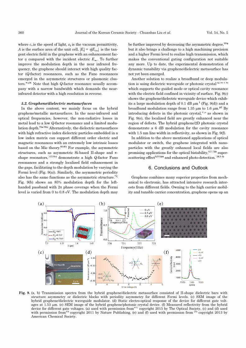
5.2. Graphene/dielectric metasurfaces
In the above content, we mainly focus on the hybrid
graphene/metallic metasurfaces. In the near-infrared and
optical frequencies, however, the non-radiative losses in
metal lead to a low Q-factor resonance and a limited modu-
lation depth.114-116) Alternatively, the dielectric metasurfaces
with high refractive index dielectric particles embedded in a
low index matrix can support different order electric and
magnetic resonances with an extremely low intrinsic losses
based on the Mie theory.61-63) For example, the asymmetric
structures, such as asymmetric Si-based II-shape and π-
shape resonators,117,118) demonstrate a high Q-factor Fano
resonances and a strongly localized field enhancement in
the gaps, facilitating to the depth modulation by varying the
Fermi level (Fig. 9(a)). Similarly, the asymmetric periodity
also has the same functions as the asymmetric structure.75)
Fig. 9(b) shows an 85% modulation depth for the left-
handed passband with 2π phase coverage when the Fermi
level is varied from 0 to 0.8 eV. The modulation depth may
be further improved by decreasing the asymmetric degree,119)
but it also brings a challenge to a high machining precision
and a higher Fermi level to realize high transmission, which
makes the conventional gating configuration not suitable
any more. Up to date, the experimental demonstration of
dynamic tunability via graphene/dielectric metasurface has
not yet been emerged.
Another solution to realize a broadband or deep modula-
tion is using dielectric waveguide or photonic crystal16,120-124)
which supports the guided mode or optical cavity resonance
with the electric field confined in vicinity of surface. Fig. 9(c)
shows the graphene/dielectric waveguide device which exhib-
its a large modulation depth of 0.1 dB μm-1 (Fig. 9(d)) and a
broadband modulation range from 1.35 μm to 1.6 μm.16) By
introducing defects in the photonic crystal,123) as shown in
Fig. 9(e), the localized field are greatly enhanced near the
region of defects. The hybrid graphene/2D photonic crystal
demonstrate a 6 dB modulation for the cavity resonance
with 1.5 nm line width in reflectivity, as shown in Fig. 9(f).
In addition to the above mentioned applications of optical
modulator or switch, the graphene integrated with nano-
particles with the greatly enhanced local fields are also
promising applications for the optical bistability,125,126) super-
scattering effect127-129) and enhanced photo-detection.130,131)
6. Conclusions and Outlook
Graphene combines many superior properties from mech-
anical to electronic, has attracted intensive research inter-
ests from different fields. Owning to the high carrier mobil-
ity and tunable carrier concentration, graphene opens up an
Et = η Einc
Fig. 9. (a, b) Transmission spectra from the hybrid graphene/dielectric metasurface consisted of II-shape dielectric bars withstructure asymmetry or dielectric blocks with periodity asymmetry for different Fermi levels. (c) SEM image of thehybrid graphene/dielectric waveguide modulator. (d) Static electro-optical response of the device for different gate volt-ages at 1.53 µm. (e) SEM image of the hybrid graphene/photonic crystal device. (f) Measured reflectivity from the hybriddevice for different gate voltages. (a) used with permission from117) copyright 2015 by The Optical Society, (c) and (d) usedwith permission from16) copyright 2011 by Nature Publishing, (e) and (f) used with permission from123) copyright 2013 byAmerican Chemical Society.

September 2017 A Review of Graphene Plasmons and its Combination with Metasurface 361
exciting opportunity to high performance applications, such
as plasmonics, optoelectronic devices based on graphene
plasmons. Different from noble metal plasmons in range of
visible frequencies, graphene plasmons operate from tera-
hertz to mid-infrared frequencies and demonstrate an ex-
tremely high confinement, facilitating to light-matter inter-
action for quantum optics, chemical identifications and bio-
sensors. Importantly, the tunable surface conductivity makes
graphene a wider application prospect. Graphene inte-
grated with silicon-based optical circuit can dynamically
manipulate the amplitude, phase and polarization of light,
promising applications for optical communication and opti-
cal computing. Besides, graphene can couple with metasur-
faces of enhanced local electric field to improve the optical
modulation depth.
The behavior of graphene plasmons is tightly associated
with the graphene itself. Large-scale grown high quality
graphene is desirable in many applications and has been
realized by chemical vapor deposition (CVD) on copper foils
and films. However, the following transfer process is usu-
ally very complicated and need be optimized to minimize
the damage to graphene. Another important challenge is
the fabrication of structured graphene with fine control of
shape and quality which will significantly influence the
graphene plasmons.
Note that except for the graphene, many 2D materials,
such as black phosphorus, molybdenum disulfide and topo-
logical insulators, also demonstrate the similar or even pref-
erable electrical and optical properties which can be used to
explore the tunable collective optical oscillations.
Acknowledgments
This work was supported by grants from the National
Youth Top-Notch Talent Support Program and the Funda-
mental Research Funds for the Central Universities.
REFERENCES
1. K. S. Novoselov, A. K. Geim, S. V. Morozov, D. Jiang, Y.Zhang, S. V. Dubonos, I. V. Grigorieva, and A. A. Firsov,“Electric Field Effect in Atomically Thin Carbon Films,”Science, 306 [5696] 666-69 (2004).
2. A. C. Neto, F. Guinea, N. M. Peres, K. S. Novoselov, andA. K. Geim, “The Electronic Properties of Graphene,” Rev.
Mod. Phys., 81 [1] 109 (2009). 3. L. Falkovsky, “Optical Properties of Graphene,” J. Phys.:
Conf. Ser., 129 [1] 012004 (2008). 4. M. C. Lemme, T. J. Echtermeyer, M. Baus, and H. Kurz,
“A Graphene Field-Effect Device,” IEEE Electron Device
Lett., 28 [4] 282-84 (2007). 5. F. Bonaccorso, Z. Sun, T. Hasan, and A. Ferrari, “Graphene
Photonics and Optoelectronics,” Nat. Photonics, 4 [9] 611-22 (2010).
6. C. H. Lui, K. F. Mak, J. Shan, and T. F. Heinz, “UltrafastPhotoluminescence from Graphene,” Phys. Rev. Lett., 105
[12] 127404 (2010).
7. J. M. Dawlaty, S. Shivaraman, J. Strait, P. George, M.Chandrashekhar, F. Rana, M. G. Spencer, D. Veksler, andY. Chen, “Measurement of the Optical Absorption Spectraof Epitaxial Graphene from Terahertz to Visible,” Appl.
Phys. Lett., 93 [13] 131905 (2008). 8. L. Falkovsky and S. Pershoguba, “Optical Far-Infrared
Properties of a Graphene Monolayer and Multilayer,” Phys.
Rev. B, 76 [15] 153410 (2007). 9. R. R. Nair, P. Blake, A. N. Grigorenko, K. S. Novoselov, T.
J. Booth, T. Stauber, N. M. Peres, and A. K. Geim, “FineStructure Constant Defines Visual Transparency ofGraphene,” Science, 320 [5881] 1308 (2008).
10. M. Jablan, H. Buljan, and M. Soljačić, “Plasmonics inGraphene at Infrared Frequencies,” Phys. Rev. B, 80 [24]245435 (2009).
11. A. Grigorenko, M. Polini, and K. Novoselov, “GraphenePlasmonics,” Nat. Photonics, 6 [11] 749-58 (2012).
12. F. H. Koppens, D. E. Chang, and F. J. García de Abajo,“Graphene Plasmonics: A Platform for Strong Light-Matter Interactions,” Nano Lett., 11 [8] 3370-77 (2011).
13. J. Chen, M. Badioli, P. Alonso-González, S. Thongrattana-siri, F. Huth, J. Osmond, M. Spasenović, A. Centeno, A.Pesquera, and P. Godignon, “Optical Nano-Imaging ofGate-Tunable Graphene Plasmons,” Nature, 487 [7405]77-81 (2012).
14. A. Kasry, M. A. Kuroda, G. J. Martyna, G. S. Tulevski,and A. A. Bol, “Chemical Doping of Large-Area StackedGraphene Films for Use as Transparent, ConductingElectrodes,” ACS Nano., 4 [7] 3839-44 (2010).
15. F. Wang, Y. Zhang, C. Tian, C. Girit, A. Zettl, M. Crom-mie, and Y. R. Shen, “Gate-Variable Optical Transitionsin Graphene,” Science, 320 [5873] 206-9 (2008).
16. M. Liu, X. Yin, E. Ulin-Avila, B. Geng, T. Zentgraf, L. Ju,F. Wang, and X. Zhang, “A Graphene-based BroadbandOptical Modulator,” Nature, 474 [7349] 64-7 (2011).
17. A. Y. Nikitin, F. Guinea, F. Garcia-Vidal, and L. Martin-Moreno, “Fields Radiated by a Nanoemitter in a GrapheneSheet,” Phys. Rev. B, 84 [19] 195446 (2011).
18. Y. Bao, S. Zu, Y. Zhang, and Z. Fang, “Active Control ofGraphene-based Unidirectional Surface Plasmon Launcher,”ACS Photonics, 2 [8] 1135-40 (2015).
19. Z. Fei, A. S. Rodin, G. O. Andreev, W. Bao, A. S. McLeod,M. Wagner, L. M. Zhang, Z. Zhao, M. Thiemens, G.Dominguez, M. M. Fogler, A. H. C. Neto, C. N. Lau, F.Keilmann, and D. N. Basov, “Gate-Tuning of GraphenePlasmons Revealed by Infrared Nano-Imaging,” Nature,
487 [7405] 82-5 (2012). 20. J. A. Gerber, S. Berweger, B. T. O’Callahan, and M. B.
Raschke, “Phase-Resolved Surface Plasmon Interferometryof Graphene,” Phys. Rev. Lett., 113 [5] 055502 (2014).
21. G. X. Ni, L. Wang, M. D. Goldflam, M. Wagner, Z. Fei, A.S. McLeod, M. K. Liu, F. Keilmann, B. Özyilmaz, A. H.Castro Neto, J. Hone, M. M. Fogler, and D. N. Basov,“Ultrafast Optical Switching of Infrared Plasmon Polaritonsin High-Mobility Graphene,” Nat. Photonics, 10 [4] 244-47(2016).
22. W. Zhou, J. Lee, J. Nanda, S. T. Pantelides, S. J. Penny-cook, and J.-C. Idrobo, “Atomically Localized PlasmonEnhancement in Monolayer Graphene,” Nat. Nanotech-

362 Journal of the Korean Ceramic Society - Chuanbao Liu et al. Vol. 54, No. 5
nol., 7 [3] 161-65 (2012). 23. Z. Fei, A. S. Rodin, W. Gannett, S. Dai, W. Regan, M.
Wagner, M. K. Liu, A. S. McLeod, G. Dominguez, M. Thie-mens, Antonio H. Castro Neto, F. Keilmann, A. Zettl, R.Hillenbrand, M. M. Fogler, and D. N. Basov, “Electronicand Plasmonic Phenomena at Graphene Grain Boundaries,”Nat. Nanotechnol., 8 [11] 821-25 (2013).
24. W. Gao, G. Shi, Z. Jin, J. Shu, Q. Zhang, R. Vajtai, P. M.Ajayan, J. Kono, and Q. Xu, “Excitation and Active Controlof Propagating Surface Plasmon Polaritons in Graphene,”Nano Lett., 13 [8] 3698-702 (2013).
25. W. Gao, J. Shu, C. Qiu, and Q. Xu, “Excitation of PlasmonicWaves in Graphene by Guided-Mode Resonances,” ACS
Nano., 6 [9] 7806-13 (2012). 26. H. Lu, J. Zhao, and M. Gu, “Nanowires-Assisted Excitation
and Propagation of Mid-Infrared Surface Plasmon Polaritonsin Graphene,” J. Appl. Phys., 120 [16] 163106 (2016).
27. Y. Zhao, G. Chen, Z. Tao, C. Zhang, and Y. Zhu, “High Q-Factor Plasmonic Resonators in Continuous GrapheneExcited by Insulator-Covered Silicon Gratings,” RSC
Adv., 4 [50] 26535-42 (2014). 28. Y. V. Bludov, M. Vasilevskiy, and N. Peres, “Mechanism
for Graphene-based Optoelectronic Switches by TuningSurface Plasmon-Polaritons in Monolayer Graphene,”Europhys. Lett., 92 [6] 68001 (2011).
29. A. Y. Nikitin, P. Alonso-González, and R. Hillenbrand,“Efficient Coupling of Light to Graphene Plasmons byCompressing Surface Polaritons with Tapered BulkMaterials,” Nano Lett., 14 [5] 2896-901 (2014).
30. V. W. Brar, M. S. Jang, M. Sherrott, J. J. Lopez, and H. A.Atwater, “Highly Confined Tunable Mid-Infrared Plasmonicsin Graphene Nanoresonators,” Nano Lett., 13 [6] 2541-47(2013).
31. H. Hu, X. Yang, F. Zhai, D. Hu, R. Liu, K. Liu, Z. Sun, andQ. Dai, “Far-Field Nanoscale Infrared Spectroscopy ofVibrational Fingerprints of Molecules with GraphenePlasmons,” Nat. Commun., 7 12334 (2016).
32. L. Ju, B. Geng, J. Horng, C. Girit, M. Martin, Z. Hao, H.A. Bechtel, X. Liang, A. Zettl, and Y. R. Shen, “GraphenePlasmonics for Tunable Terahertz Metamaterials,” Nat.
Nanotechnol., 6 [10] 630-34 (2011). 33. H. Yan, T. Low, W. Zhu, Y. Wu, M. Freitag, X. Li, F. Guinea,
P. Avouris, and F. Xia, “Damping Pathways of Mid-Infrared Plasmons in Graphene Nanostructures,” Nat.
Photonics, 7 [5] 394-99 (2013). 34. D. Rodrigo, O. Limaj, D. Janner, D. Etezadi, F. J. G. de
Abajo, V. Pruneri, and H. Altug, “Mid-Infrared PlasmonicBiosensing with Graphene,” Science, 349 [6244] 165-68(2015).
35. F. J. Garcia de Abajo, “Graphene Plasmonics: Challengesand Opportunities,” ACS Photonics, 1 [3] 135-52 (2014).
36. Z. Fang, S. Thongrattanasiri, A. Schlather, Z. Liu, L. Ma,Y. Wang, P. M. Ajayan, P. Nordlander, N. J. Halas, and F.J. García de Abajo, “Gated Tunability and Hybridizationof Localized Plasmons in Nanostructured Graphene,”ACS Nano., 7 [3] 2388-95 (2013).
37. H. Yan, X. Li, B. Chandra, G. Tulevski, Y. Wu, M. Freitag,W. Zhu, P. Avouris, and F. Xia, “Tunable Infrared PlasmonicDevices Using Graphene/Insulator Stacks,” Nat. Nano-
technol., 7 [5] 330-34 (2012). 38. T. Guo and C. Argyropoulos, “Broadband Polarizers based
on Graphene Metasurfaces,” Opt. Lett., 41 [23] 5592-95(2016).
39. A. Fallahi and J. Perruisseau-Carrier, “Design of TunableBiperiodic Graphene Metasurfaces,” Phys. Rev. B, 86 [19]195408 (2012).
40. H. Cheng, S. Chen, P. Yu, J. Li, L. Deng, and J. Tian,“Mid-Infrared Tunable Optical Polarization ConverterComposed of Asymmetric Graphene Nanocrosses,” Opt.
Lett., 38 [9] 1567-69 (2013). 41. F. Lu, B. Liu, and S. Shen, “Infrared Wavefront Control
based on Graphene Metasurfaces,” Adv. Opt. Mater., 2 [8]794-99 (2014).
42. T. Yatooshi, A. Ishikawa, and K. Tsuruta, “Terahertz Wave-front Control by Tunable Metasurface Made of GrapheneRibbons,” Appl. Phys. Lett., 107 [5] 053105 (2015).
43. Z. Li, K. Yao, F. Xia, S. Shen, J. Tian, and Y. Liu, “GraphenePlasmonic Metasurfaces to Steer Infrared Light,” Sci.
Rep., 5 12423 (2015). 44. X. Hu, L. Wen, S. Song, and Q. Chen, “Tunable Graphene
Metasurfaces by Discontinuous Pancharatnam-Berry PhaseShift,” Nanotechnology, 26 [50] 505203 (2015).
45. N. Dabidian, I. Kholmanov, A. B. Khanikaev, K. Tatar, S.Trendafilov, S. H. Mousavi, C. Magnuson, R. S. Ruoff, andG. Shvets, “Electrical Switching of Infrared Light UsingGraphene Integration with Plasmonic Fano ResonantMetasurfaces,” ACS Photonics, 2 [2] 216-27 (2015).
46. N. K. Emani, T.-F. Chung, A. V. Kildishev, V. M. Shalaev,Y. P. Chen, and A. Boltasseva, “Electrical Modulation ofFano Resonance in Plasmonic Nanostructures UsingGraphene,” Nano Lett., 14 [1] 78-82 (2013).
47. S. H. Lee, M. Choi, T.-T. Kim, S. Lee, M. Liu, X. Yin, H. K.Choi, S. S. Lee, C.-G. Choi, and S.-Y. Choi, “SwitchingTerahertz Waves with Gate-Controlled Active GrapheneMetamaterials,” Nat. Mater., 11 [11] 936-41 (2012).
48. M. M. Jadidi, A. B. Sushkov, R. L. Myers-Ward, A. K.Boyd, K. M. Daniels, D. K. Gaskill, M. S. Fuhrer, H. D.Drew, and T. E. Murphy, “Tunable Terahertz HybridMetal-Graphene Plasmons,” Nano Lett., 15 [10] 7099-104(2015).
49. X. Ni, A. V. Kildishev, and V. M. Shalaev, “MetasurfaceHolograms for Visible Light,” Nat. Commun., 4 2807 (2013).
50. G. Zheng, H. Mühlenbernd, M. Kenney, G. Li, T. Zentgraf,and S. Zhang, “Metasurface Holograms Reaching 80%Efficiency,” Nat. Nanotechnol., 10 [4] 308-12 (2015).
51. D. Wen, F. Yue, G. Li, G. Zheng, K. Chan, S. Chen, M.Chen, K. F. Li, P. W. H. Wong, K. W. Cheah, E. Yue BunPun, S. Zhang, and X. Chen, “Helicity Multiplexed Broad-band Metasurface Holograms,” Nat. Commun., 6 8241(2015).
52. X. Ni, S. Ishii, A. V. Kildishev, and V. M. Shalaev, “Ultra-Thin, Planar, Babinet-Inverted Plasmonic Metalenses,”Light Sci. Appl., 2 [4] e72 (2013).
53. F. Aieta, P. Genevet, M. A. Kats, N. Yu, and R. Blanchard,“Aberration-free Ultrathin Flat Lenses and Axicons atTelecom Wavelengths based on Plasmonic Metasurfaces,”Nano Lett., 12 4932-36 (2012).
54. M. Kang, T. Feng, H.-T. Wang, and J. Li, “Wave Front

September 2017 A Review of Graphene Plasmons and its Combination with Metasurface 363
Engineering from an Array of Thin Aperture Antennas,”Opt. Express, 20 [14] 15882-90 (2012).
55. C. Liu, Y. Bai, L. Jing, Y. Yang, H. Chen, J. Zhou, Q. Zhao,and L. Qiao, “Equivalent Energy Level HybridizationApproach for High-Performance Metamaterials Design,”Acta Mater., 135 [15] 144-49 (2017).
56. N. Yu, P. Genevet, M. A. Kats, F. Aieta, J.-P. Tetienne, F.Capasso, and Z. Gaburro, “Light Propagation with PhaseDiscontinuities: Generalized Laws of Reflection andRefraction,” Science, 334 [6054] 333-37 (2011).
57. C. Liu, Y. Bai, Q. Zhao, Y. Yang, H. Chen, J. Zhou, and L.Qiao, “Fully Controllable Pancharatnam-Berry MetasurfaceArray with High Conversion Efficiency and BroadBandwidth,” Sci. Rep., 6 34819 (2016).
58. X. Ni, N. K. Emani, A. V. Kildishev, A. Boltasseva, and V.M. Shalaev, “Broadband Light Bending with PlasmonicNanoantennas,” Science, 335 [6067] 427 (2012).
59. D. R. Smith, W. J. Padilla, D. C. Vier, S. C. Nemat-Nasser,and S. Schultz, “Composite Medium with SimultaneouslyNegative Permeability and Permittivity,” Phys. Rev. Lett.,
84 [18] 4184-87 (2000). 60. D. Schurig, J. J. Mock, B. J. Justice, S. A. Cummer, J. B.
Pendry, A. F. Starr, and D. R. Smith, “MetamaterialElectromagnetic Cloak at Microwave Frequencies,” Sci-
ence, 314[5801] 977-80 (2006). 61. Y. Yang, W. Wang, P. Moitra, I. I. Kravchenko, D. P.
Briggs, and J. Valentine, “Dielectric Meta-Reflectarray forBroadband Linear Polarization Conversion and OpticalVortex Generation,” Nano Lett., 14 [3] 1394-99 (2014).
62. K. E. Chong, I. Staude, A. James, J. Dominguez, S. Liu, S.Campione, G. S. Subramania, T. S. Luk, M. Decker, andD. N. Neshev, “Polarization-Independent Silicon Metadevicesfor Efficient Optical Wavefront Control,” Nano Lett., 15
[8] 5369-74 (2015). 63. M. I. Shalaev, J. Sun, A. Tsukernik, A. Pandey, K. Nikols-
kiy, and N. M. Litchinitser, “High-Efficiency All-DielectricMetasurfaces for Ultracompact Beam Manipulation inTransmission Mode,” Nano Lett., 15 [9] 6261-66 (2015).
64. W. Gao, J. Shu, K. Reichel, D. V. Nickel, X. He, G. Shi, R.Vajtai, P. M. Ajayan, J. Kono, and D. M. Mittleman, “High-Contrast Terahertz Wave Modulation by Gated GrapheneEnhanced by Extraordinary Transmission through RingApertures,” Nano Lett., 14 [3] 1242-48 (2014).
65. Y. Yao, R. Shankar, M. A. Kats, Y. Song, J. Kong, M. Lon-car, and F. Capasso, “Electrically Tunable MetasurfacePerfect Absorbers for Ultrathin Mid-Infrared OpticalModulators,” Nano Lett., 14 [11] 6526-32 (2014).
66. Z. Miao, Q. Wu, X. Li, Q. He, K. Ding, Z. An, Y. Zhang,and L. Zhou, “Widely Tunable Terahertz Phase Modulationwith Gate-Controlled Graphene Metasurfaces,” Phys. Rev.
X, 5 [4] 041027 (2015). 67. N. Dabidian, S. Dutta-Gupta, I. Kholmanov, K. Lai, F. Lu,
J. Lee, M. Jin, S. Trendafilov, A. Khanikaev, and B. Falla-hazad, “Experimental Demonstration of Phase Modulationand Motion Sensing Using Graphene-Integrated Meta-surfaces,” Nano Lett., 16 [6] 3607-15 (2016).
68. Z. Fang, Z. Liu, Y. Wang, P. M. Ajayan, P. Nordlander,and N. J. Halas, “Graphene-Antenna Sandwich Photo-detector,” Nano Lett., 12 [7] 3808-13 (2012).
69. Y. Fan, N. H. Shen, F. Zhang, Z. Wei, H. Li, Q. Zhao, Q.Fu, P. Zhang, T. Koschny, and C. M. Soukoulis, “Electri-cally Tunable Goos-Hänchen Effect with Graphene in theTerahertz Regime,” Adv. Opt. Mater., 4 [11] 1824-28 (2016).
70. K. S. Kim, Y. Zhao, H. Jang, S. Y. Lee, J. M. Kim, K. S.Kim, J.-H. Ahn, P. Kim, J.-Y. Choi, and B. H. Hong, “Large-Scale Pattern Growth of Graphene Films for StretchableTransparent Electrodes,” Nature, 457 [7230] 706 (2009).
71. X. Li, C. W. Magnuson, A. Venugopal, R. M. Tromp, J. B.Hannon, E. M. Vogel, L. Colombo, and R. S. Ruoff, “Large-Area Graphene Single Crystals Grown by Low-PressureChemical Vapor Deposition of Methane on Copper,” J.
Am. Chem. Soc., 133 [9] 2816-19 (2011). 72. E. V. Castro, H. Ochoa, M. Katsnelson, R. Gorbachev, D.
Elias, K. Novoselov, A. Geim, and F. Guinea, “Limits onCharge Carrier Mobility in Suspended Graphene due toFlexural Phonons,” Phys. Rev. Lett., 105 [26] 266601 (2010).
73. C.-F. Chen, C.-H. Park, B. W. Boudouris, J. Horng, B.Geng, C. Girit, A. Zettl, M. F. Crommie, R. A. Segalman,S. G. Louie, and F. Wang, “Controlling Inelastic LightScattering Quantum Pathways in Graphene,” Nature,
471 [7340] 617-20 (2011). 74. J. Kim, H. Son, D. J. Cho, B. Geng, W. Regan, S. Shi, K.
Kim, A. Zettl, Y.-R. Shen, and F. Wang, “Electrical Controlof Optical Plasmon Resonance with Graphene,” Nano
Lett., 12 [11] 5598-602 (2012). 75. C. Liu, Y. Bai, J. Zhou, Q. Zhao, and L. Qiao, “Large-Scale
Modulation of Left-Ganded Passband in Gybrid Graphene/Dielectric Metasurface,” Ann. Phys., 529 [8] 1700125(2017).
76. Z. Fang, Y. Wang, Z. Liu, A. Schlather, P. M. Ajayan, F.H. Koppens, P. Nordlander, and N. J. Halas, “Plasmon-Induced Doping of Graphene,” ACS Nano., 6 [11] 10222-28 (2012).
77. H. Yan, Z. Li, X. Li, W. Zhu, P. Avouris, and F. Xia, “Infra-red Spectroscopy of Tunable Dirac Terahertz Magneto-Plasmons in Graphene,” Nano Lett., 12 [7] 3766-71 (2012).
78. V. P. Verma, S. Das, I. Lahiri, and W. Choi, “Large-AreaGraphene on Polymer Film for Flexible and TransparentAnode in Field Emission Device,” Appl. Phys. Lett., 96 [20]203108 (2010).
79. F. Schedin, E. Lidorikis, A. Lombardo, V. G. Kravets, A.K. Geim, A. N. Grigorenko, K. S. Novoselov, and A. C. Fer-rari, “Surface-Enhanced Raman Spectroscopy of Graphene,”ACS Nano., 4 [10] 5617-26 (2010).
80. S. Mikhailov and K. Ziegler, “New Electromagnetic Modein Graphene,” Phys. Rev. Lett., 99 [1] 016803 (2007).
81. Y. Liu, R. F. Willis, K. Emtsev, and T. Seyller, “PlasmonDispersion and Damping in Electrically Isolated Two-Dimensional Charge Sheets,” Phys. Rev. B, 78 [20] 201403(2008).
82. Z. Fei, G. O. Andreev, W. Bao, L. M. Zhang, A. S. McLeod,C. Wang, M. K. Stewart, Z. Zhao, G. Dominguez, and M.Thiemens, “Infrared Nanoscopy of Dirac Plasmons at theGraphene-SiO2 Interface,” Nano Lett., 11 [11] 4701-5 (2011).
83. W. L. Barnes, A. Dereux, and T. W. Ebbesen, “SurfacePlasmon Subwavelength Optics,” Nature, 424 [6950] 824(2003).
84. A. Vakil and N. Engheta, “Transformation Optics Using

364 Journal of the Korean Ceramic Society - Chuanbao Liu et al. Vol. 54, No. 5
Graphene,” Science, 332 [6035] 1291-94 (2011). 85. A. Otto, “Excitation of Nonradiative Surface Plasma Waves
in Silver by the Method of Frustrated Total Reflection,” Z.
Phys., 216 [4] 398-410 (1968). 86. E. Kretschmann and H. Raether, “Radiative Decay of Non
Radiative Surface Plasmons Excited by Light,” Z. Natur-
forsch. A, 23 [12] 2135-36 (1968). 87. P. Alonso-González, A. Y. Nikitin, F. Golmar, A. Centeno,
A. Pesquera, S. Vélez, J. Chen, G. Navickaite, F. Koppens,and A. Zurutuza, “Controlling Graphene Plasmons withResonant Metal Antennas and Spatial ConductivityPatterns,” Science, 344 [6190] 1369-73 (2014).
88. B. Wang, X. Zhang, X. Yuan, and J. Teng, “Optical Couplingof Surface Plasmons between Graphene Sheets,” Appl.
Phys. Lett., 100 [13] 131111 (2012). 89. B. Wang, X. Zhang, F. J. García-Vidal, X. Yuan, and J.
Teng, “Strong Coupling of Surface Plasmon Polaritons inMonolayer Graphene Sheet Arrays,” Phys. Rev. Lett., 109
[7] 073901 (2012). 90. A. Y. Nikitin, F. Guinea, F. J. García-Vidal, and L.
Martín-Moreno, “Edge and Waveguide Terahertz SurfacePlasmon Modes in Graphene Microribbons,” Phys. Rev. B,
84 [16] 161407 (2011). 91. J. Christensen, A. Manjavacas, S. Thongrattanasiri, F. H.
Koppens, and F. J. García de Abajo, “Graphene PlasmonWaveguiding and Hybridization in Individual and PairedNanoribbons,” ACS Nano., 6 [1] 431-40 (2011).
92. A. Y. Nikitin, F. Guinea, F. J. Garcia-Vidal, and L. Mar-tin-Moreno, “Surface Plasmon Enhanced Absorption andSuppressed Transmission in Periodic Arrays of Grapheneribbons,” Phys. Rev. B, 85 [8] 081405 (2012).
93. B. Sensale-Rodriguez, R. Yan, M. M. Kelly, T. Fang, K.Tahy, W. S. Hwang, D. Jena, L. Liu, and H. G. Xing,“Broadband Graphene Terahertz Modulators Enabled byIntraband Transitions,” Nat. Commun., 3 780 (2012).
94. S. Thongrattanasiri, F. H. Koppens, and F. J. G. De Abajo,“Complete Optical Absorption in Periodically PatternedGraphene,” Phys. Rev. Lett., 108 [4] 047401 (2012).
95. Y. Fan, F. Zhang, Q. Zhao, Z. Wei, and H. Li, “TunableTerahertz Coherent Perfect Absorption in a MonolayerGraphene,” Opt. Lett., 39 [21] 6269-72 (2014).
96. Y. Fan, N.-H. Shen, T. Koschny, and C. M. Soukoulis,“Tunable Terahertz Meta-Surface with Graphene Cut-Wires,” ACS Photonics, 2 [1] 151-56 (2015).
97. Y. Fan, Z. Wei, Z. Zhang, and H. Li, “Enhancing InfraredExtinction and Absorption in a Monolayer GrapheneSheet by Harvesting the Electric Dipolar Mode of SplitRing Resonators,” Opt. Lett., 38 [24] 5410-13 (2013).
98. T. V. Teperik, F. G. De Abajo, A. Borisov, M. Abdelsalam,P. Bartlett, Y. Sugawara, and J. Baumberg, “Omnidirec-tional Absorption in Nanostructured Metal Surfaces,”Nature Photon., 2 [5] 299-301 (2008).
99. M. S. Jang, V. W. Brar, M. C. Sherrott, J. J. Lopez, L.Kim, S. Kim, M. Choi, and H. A. Atwater, “Tunable LargeResonant Absorption in a Midinfrared Graphene Salis-bury Screen,” Phys. Rev. B, 90 [16] 165409 (2014).
100. R. Alaee, M. Farhat, C. Rockstuhl, and F. Lederer, “APerfect Absorber Made of a Graphene Micro-Ribbon Meta-material,” Opt. Express, 20 [27] 28017-24 (2012).
101. A. Andryieuski and A. V. Lavrinenko, “Graphene Meta-materials based Tunable Terahertz Absorber: EffectiveSurface Conductivity Approach,” Opt. Express, 21 [7] 9144-55 (2013).
102. P.-Y. Chen, H. Huang, D. Akinwande, and A. Alú,“Graphene-based Plasmonic Platform for ReconfigurableTerahertz Nanodevices,” ACS Photonics, 1 [8] 647-54(2014).
103. S. F. Shi, B. Zeng, H. L. Han, X. Hong, H. Z. Tsai, H. S.Jung, A. Zettl, M. F. Crommie, and F. Wang, “OptimizingBroadband Terahertz Modulation with Hybrid Graphene/Metasurface Structures,” Nano Lett., 15 [1] 372-77 (2015).
104. Q. Li, L. Cong, R. Singh, N. Xu, W. Cao, X. Zhang, Z. Tian,L. Du, J. Han, and W. Zhang, “Monolayer GrapheneSensing Enabled by the Strong Fano-Resonant Meta-surface,” Nanoscale, 8 [39] 17278-84 (2016).
105. Q. Li, Z. Tian, X. Zhang, N. Xu, R. Singh, J. Gu, P. Lv, L.-B. Luo, S. Zhang, J. Han, and W. Zhang, “Dual Control ofActive Graphene-Silicon Hybrid Metamaterial Devices,”Carbon, 90 146-53 (2015).
106. N. K. Emani, T.-F. Chung, X. Ni, A. V. Kildishev, Y. P.Chen, and A. Boltasseva, “Electrically Tunable Dampingof Plasmonic Resonances with Graphene,” Nano Lett., 12
[10] 5202-6 (2012). 107. Y. Yao, M. A. Kats, P. Genevet, N. Yu, Y. Song, J. Kong,
and F. Capasso, “Broad Electrical Tuning of Graphene-Loaded Plasmonic Antennas,” Nano Lett., 13 [3] 1257-64(2013).
108. Y. Yao, R. Shankar, P. Rauter, Y. Song, J. Kong, M. Lon-car, and F. Capasso, “High-Responsivity Mid-InfraredGraphene Detectors with Antenna-Enhanced PhotocarrierGeneration and Collection,” Nano Lett., 14 [7] 3749-54(2014).
109. S. H. Mousavi, I. Kholmanov, K. B. Alici, D. Purtseladze,N. Arju, K. Tatar, D. Y. Fozdar, J. W. Suk, Y. Hao, and A.B. Khanikaev, “Inductive Tuning of Fano-Resonant Meta-surfaces Using Plasmonic Response of Graphene in theMid-Infrared,” Nano Lett., 13 [3] 1111-17 (2013).
110. D. A. Smirnova, A. E. Miroshnichenko, Y. S. Kivshar, andA. B. Khanikaev, “Tunable Nonlinear Graphene Meta-surfaces,” Phys. Rev. B, 92 [16] 161406 (2015).
111. Y. Yao, M. A. Kats, R. Shankar, Y. Song, J. Kong, M. Lon-car, and F. Capasso, “Wide Wavelength Tuning of OpticalAntennas on Graphene with Nanosecond Response Time,”Nano Lett., 14 [1] 214-19 (2013).
112. B. Luk'yanchuk, N. I. Zheludev, S. A. Maier, N. J. Halas,P. Nordlander, H. Giessen, and C. T. Chong, “The FanoResonance in Plasmonic Nanostructures and Metamaterials,”Nature Mater., 9 [9] 707-15 (2010).
113. A. E. Miroshnichenko, S. Flach, and Y. S. Kivshar, “FanoResonances in Nanoscale Structures,” Rev. Mod. Phys., 82
[3] 2257 (2010). 114. B. Zhao, J. Zhao, and Z. Zhang, “Enhancement of Near-
Infrared Absorption in Graphene with Metal Gratings,”Appl. Phys. Lett., 105 [3] 031905 (2014).
115. A. Boltasseva and H. A. Atwater, “Low-Loss PlasmonicMetamaterials,” Science, 331 [6015] 290-91 (2011).
116. P. R. West, S. Ishii, G. V. Naik, N. K. Emani, V. M. Sha-laev, and A. Boltasseva, “Searching for Better Plasmonic

September 2017 A Review of Graphene Plasmons and its Combination with Metasurface 365
Materials,” Laser Photonics Rev., 4 [6] 795-808 (2010). 117. C. Argyropoulos, “Enhanced Transmission Modulation
Based on Dielectric Metasurfaces Loaded with Graphene,”Opt. Express, 23 [18] 23787-97 (2015).
118. C. Wu, N. Arju, G. Kelp, J. A. Fan, J. Dominguez, E. Gon-zales, E. Tutuc, I. Brener, and G. Shvets, “SpectrallySelective Chiral Silicon Metasurfaces based on InfraredFano Resonances,” Nat. Commun., 27 [5] 3892 (2014).
119. J. Zhang, W. Liu, Z. Zhu, X. Yuan, and S. Qin, “StrongField Enhancement and Light-Matter Interactions withAll-Dielectric Metamaterials based on Split Bar Reson-ators,” Opt. Express, 22 [25] 30889-98 (2014).
120. S. Wu, S. Buckley, A. M. Jones, J. S. Ross, N. J. Ghimire,J. Yan, D. G. Mandrus, W. Yao, F. Hatami, and J. Vučković,“Control of Two-Dimensional Excitonic Light Emissionvia Photonic Crystal,” 2D Mater., 1 [1] 011001 (2014).
121. R. Li, M. Imran, X. Lin, H. Wang, Z. Xu, and H. Chen,“Hybrid Airy Plasmons with Dynamically Steerable Tra-jectories,” Nanoscale, 9 [4] 1449-56 (2017).
122. R.-J. Shiue, X. Gan, Y. Gao, L. Li, X. Yao, A. Szep, D.Walker Jr, J. Hone, and D. Englund, “Enhanced Photo-detection in Graphene-Integrated Photonic Crystal Cavity,”Appl. Phys. Lett., 103 [24] 241109 (2013).
123. A. Majumdar, J. Kim, J. Vuckovic, and F. Wang, “Electri-cal Control of Silicon Photonic Crystal Cavity by Graphene,”Nano Lett., 13 [2] 515-18 (2013).
124. Y. Fan, Z. Wei, H. Li, H. Chen, and C. M. Soukoulis, “Pho-
tonic Band Gap of a Graphene-Embedded Quarter-WaveStack,” Phys. Rev. B, 88 [24] 241403 (2013).
125. R. Li, H. Wang, B. Zheng, S. Dehdashti, E. Li, and H.Chen, “Bistable Scattering in Graphene-Coated DielectricNanowires,” Nanoscale, 9 8449-57 (2017).
126. R. Li, X. Lin, S. Lin, X. Zhang, E. Li, and H. Chen, “Graph-ene Induced Mode Bifurcation at Low Input Power,” Car-
bon, 98 463-67 (2016). 127. R. Li, X. Lin, S. Lin, X. Liu, and H. Chen, “Tunable Deep-
Subwavelength Superscattering Using Graphene Mono-layers,” Opt. Lett., 40 [8] 1651-54 (2015).
128. R. Li, X. Lin, S. Lin, X. Liu, and H. Chen, “AtomicallyThin Spherical Shell-Shaped Superscatterers based on aBohr Model,” Nanotechnology, 26 [50] 505201 (2015).
129. R. Li, B. Zheng, X. Lin, R. Hao, S. Lin, W. Yin, E. Li, andH. Chen, “Design of Ultracompact Graphene-Based Super-scatterers,” IEEE J. Sel. Top. Quantum Electron., 23 [1]130-37 (2017).
130. Y. Liu, R. Cheng, L. Liao, H. Zhou, J. Bai, G. Liu, L. Liu,Y. Huang, and X. Duan, “Plasmon Resonance EnhancedMulticolour Photodetection by Graphene,” Nat. Commun.,
2 579 (2011). 131. T. J. Echtermeyer, L. Britnell, P. K. Jasnos, A. Lombardo,
R. V. Gorbachev, A. N. Grigorenko, A. K. Geim, A. C. Fer-rari, and K. S. Novoselov, “Strong Plasmonic Enhancementof Photovoltage in Graphene,” Nat. Commun., 2 458 (2011).