a reusable high aspect ratio parylene-c shadow mask ... · a reusable high aspect ratio parylene-c...
TRANSCRIPT
A
sdhspt©
K
1
laMassmt
mows
0d
Available online at www.sciencedirect.com
Sensors and Actuators A 145–146 (2008) 306–315
A reusable high aspect ratio parylene-C shadow masktechnology for diverse micropatterning applications
S. Selvarasah a, S.H. Chao a, C.-L. Chen a, S. Sridhar b, A. Busnaina c,A. Khademhosseini d,e, M.R. Dokmeci a,∗
a Department of Electrical and Computer Engineering, Northeastern University, Boston, MA 02115, USAb Physics Department, Northeastern University, Boston, MA 02115, USA
c Department of Mechanical and Industrial Engineering, Northeastern University, Boston, MA 02115, USAd Harvard-MIT Division of Health Sciences and Technology, MIT, Cambridge, MA 02139, USA
e Department of Medicine, Center for Biomedical Engineering, Brigham and Women’s Hospital, Cambridge, MA 02139, USA
Received 3 July 2007; received in revised form 1 October 2007; accepted 14 October 2007Available online 26 October 2007
bstract
In this paper, we present a low cost, flexible and reusable parylene-C shadow mask technology for diverse micropatterning applications. Themallest feature size of 4 �m is demonstrated and the technology is scalable up to full wafer scale. With the addition of SU-8 pillars, we alsoemonstrate multimask processing with an alignment accuracy of about 4–9 �m. To achieve features with fine resolution, a low temperature and
igh aspect ratio (>8:1) parylene etch process is also developed. Utilizing this shadow mask, we successfully patterned proteins and cells on variousurfaces (glass, PDMS, methacrylate). High pattern flexibility (structures with different shapes and dimensions are successfully patterned) andatterning on curved PDMS surfaces are also demonstrated. This technology has potential applications for patterning proteins, cells and organicransistors on conventional and/or unconventional substrates.2007 Elsevier B.V. All rights reserved.
ing
pmTraflt(hratm
eywords: Parylene-C; Flexible shadow masks; High aspect ratio polymer etch
. Introduction
Classical microfabrication based on optical lithography hasimitations for applications such as patterning organic materi-ls (solvent incompatibility), patterning on fragile (released)EMS devices, patterning of non-traditional materials (proteins
nd cells), and patterning on plastic substrates (that cannot with-tand high temperatures) and on non-planar surfaces. Hence,hadow mask technology is gaining impetus as an alternativeicropatterning technique for diverse applications on conven-
ional and unconventional surfaces.Shadow masks can be classified as active or passive shadow
asks. The difference between them is that the aperture size
f the active shadow masks are adjustable within demand [1,2]hereas the passive shadow masks, which include most currenthadow masks, have a fixed aperture size. Previously reported
∗ Corresponding author. Tel.: +1 617 373 2751.E-mail address: [email protected] (M.R. Dokmeci).
ipba(
a
924-4247/$ – see front matter © 2007 Elsevier B.V. All rights reserved.oi:10.1016/j.sna.2007.10.053
assive microstencils, which are made of rigid or polymericembranes, have various limitations. For instance, Si, Si3N4,EM grid and stainless steel shadow masks are rigid and brittle,
equire complicated and expensive processing steps [3,4]. Inddition, they lack the precise pattern definition and the patternexibility to different pattern dimensions due to the gap between
he stencil and the substrate [5–8]. Elastomeric microstencilssuch as PDMS), on the other hand, are not easy to handle, andave difficulty in achieving mechanical alignment and lack highesolution [9]. Shadow masks made of SU-8 polymers [10] arelso not suitable for wafer scale patterning applications sinceheir high residual stress makes them buckle. Microstencilsade of JSR THB-430N negative UV photoresist will result
n enlargement of features due to their non-straight sidewallrofiles [11]. Furthermore, dry lift-off method as demonstratedy Ilic and Craighead is limited to thin films of single use
nd to surfaces compatible with microfabrication technologiessilicon and glass) [12].In this paper, we present a flexible, reusable, transparentnd biocompatible parylene-C microstencil technology as illus-
S. Selvarasah et al. / Sensors and Actua
tprpceti
2
icoancr[wd
stdrmsTittwci
Dsmtmicatma
3
pCoeiupptigpaeftttpsafstasu(e
ts
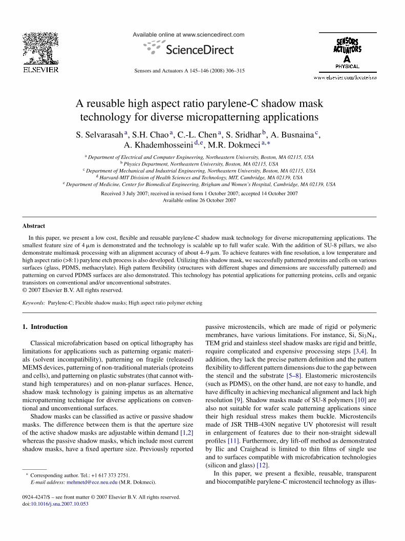
Fig. 1. The parylene shadow mask being peeled off a wafer after fabrication.
rated in Fig. 1. To realize this stencil, a novel low temperaturearylene-C etch process is developed to create the high aspectatio (HAR) structures with the use of an inductively coupledlasma (ICP) tool. The potential applications of this sten-il technology are numerous including patterning for organiclectronics, patterning of proteins and cells and patterning onopographically rough, curved and unconventional surfaces andn fabricating metamaterials.
. Parylene-C deposition
Parylene, poly-para-xylylene, is widely utilized in the med-cal and electronics industries as a conformal pinhole freeoating. Due to its high mechanical strength (tensile strengthf 3.2 GPa) it is being increasingly utilized as a structural layers well as a flexible substrate [13,14]. Up to a certain thick-ess (20 �m) the parylene films are flexible and will conform tourved surfaces and also have the high mechanical strength andobustness compared to PDMS stencils making them reusable21]. The flexible shadow mask is fabricated from parylene-Chich is deposited at room temperature and we first detail itseposition process in the following section.
Polymerizations of polymer materials are typically done inolution form or gas/vapor phase form with/without the assis-ance of plasma [15]. Parylene deposition is a chemical vaporeposition (CVD) process, which is done at 25 mTorr and atoom temperature (25 ◦C). Parylene deposition process has threeain stages. The first stage is vaporization process, where a
olid parylene dimer is vaporized at a temperature of 175 ◦C.he second stage is the pyrolysis process, during which vapor-
zed parylene gas moves slowly into the pyrolysis chamber, andhe parylene gas is decomposed into the parylene monomer at a
◦
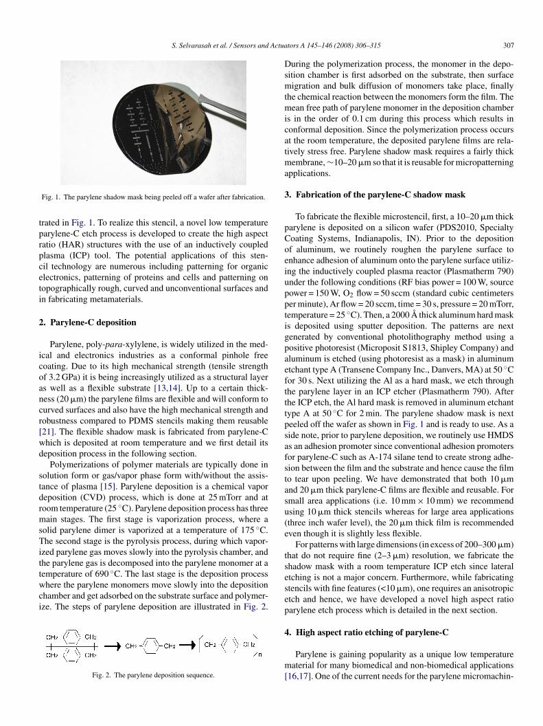
emperature of 690 C. The last stage is the deposition processhere the parylene monomers move slowly into the depositionhamber and get adsorbed on the substrate surface and polymer-ze. The steps of parylene deposition are illustrated in Fig. 2.
Fig. 2. The parylene deposition sequence.
esep
4
m[
tors A 145–146 (2008) 306–315 307
uring the polymerization process, the monomer in the depo-ition chamber is first adsorbed on the substrate, then surfaceigration and bulk diffusion of monomers take place, finally
he chemical reaction between the monomers form the film. Theean free path of parylene monomer in the deposition chamber
s in the order of 0.1 cm during this process which results inonformal deposition. Since the polymerization process occurst the room temperature, the deposited parylene films are rela-ively stress free. Parylene shadow mask requires a fairly thick
embrane, ∼10–20 �m so that it is reusable for micropatterningpplications.
. Fabrication of the parylene-C shadow mask
To fabricate the flexible microstencil, first, a 10–20 �m thickarylene is deposited on a silicon wafer (PDS2010, Specialtyoating Systems, Indianapolis, IN). Prior to the depositionf aluminum, we routinely roughen the parylene surface tonhance adhesion of aluminum onto the parylene surface utiliz-ng the inductively coupled plasma reactor (Plasmatherm 790)nder the following conditions (RF bias power = 100 W, sourceower = 150 W, O2 flow = 50 sccm (standard cubic centimeterser minute), Ar flow = 20 sccm, time = 30 s, pressure = 20 mTorr,emperature = 25 ◦C). Then, a 2000 A thick aluminum hard masks deposited using sputter deposition. The patterns are nextenerated by conventional photolithography method using aositive photoresist (Microposit S1813, Shipley Company) andluminum is etched (using photoresist as a mask) in aluminumtchant type A (Transene Company Inc., Danvers, MA) at 50 ◦Cor 30 s. Next utilizing the Al as a hard mask, we etch throughhe parylene layer in an ICP etcher (Plasmatherm 790). Afterhe ICP etch, the Al hard mask is removed in aluminum etchantype A at 50 ◦C for 2 min. The parylene shadow mask is nexteeled off the wafer as shown in Fig. 1 and is ready to use. As aide note, prior to parylene deposition, we routinely use HMDSs an adhesion promoter since conventional adhesion promotersor parylene-C such as A-174 silane tend to create strong adhe-ion between the film and the substrate and hence cause the filmo tear upon peeling. We have demonstrated that both 10 �mnd 20 �m thick parylene-C films are flexible and reusable. Formall area applications (i.e. 10 mm × 10 mm) we recommendsing 10 �m thick stencils whereas for large area applicationsthree inch wafer level), the 20 �m thick film is recommendedven though it is slightly less flexible.
For patterns with large dimensions (in excess of 200–300 �m)hat do not require fine (2–3 �m) resolution, we fabricate thehadow mask with a room temperature ICP etch since lateraltching is not a major concern. Furthermore, while fabricatingtencils with fine features (<10 �m), one requires an anisotropictch and hence, we have developed a novel high aspect ratioarylene etch process which is detailed in the next section.
. High aspect ratio etching of parylene-C
Parylene is gaining popularity as a unique low temperatureaterial for many biomedical and non-biomedical applications
16,17]. One of the current needs for the parylene micromachin-
308 S. Selvarasah et al. / Sensors and Actuators A 145–146 (2008) 306–315
Table 1ICP etch recipes for low temperature (5 ◦C) and low pressure (5 mTorr) parylene-C etching
Etch # Etch rate (�m/min) RF bias power (W) Source power (W) O2 (sscm) Ar (sccm)
abc
iamwrelss7ri“1aptmt
Ft
am
5
hdottaidmduring which the surface maintained its hydrophobic behavior
1.7 2501.0 1000.5 100
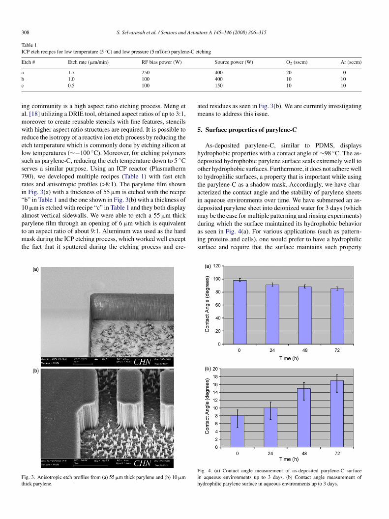
ng community is a high aspect ratio etching process. Meng etl. [18] utilizing a DRIE tool, obtained aspect ratios of up to 3:1,oreover to create reusable stencils with fine features, stencilsith higher aspect ratio structures are required. It is possible to
educe the isotropy of a reactive ion etch process by reducing thetch temperature which is commonly done by etching silicon atow temperatures (∼−100 ◦C). Moreover, for etching polymersuch as parylene-C, reducing the etch temperature down to 5 ◦Cerves a similar purpose. Using an ICP reactor (Plasmatherm90), we developed multiple recipes (Table 1) with fast etchates and anisotropic profiles (>8:1). The parylene film shownn Fig. 3(a) with a thickness of 55 �m is etched with the recipeb” in Table 1 and the one shown in Fig. 3(b) with a thickness of0 �m is etched with recipe “c” in Table 1 and they both displaylmost vertical sidewalls. We were able to etch a 55 �m thickarylene film through an opening of 6 �m which is equivalent
o an aspect ratio of about 9:1. Aluminum was used as the hardask during the ICP etching process, which worked well excepthe fact that it sputtered during the etching process and cre-
ig. 3. Anisotropic etch profiles from (a) 55 �m thick parylene and (b) 10 �mhick parylene.
ais
Fih
400 20 0400 10 10150 10 10
ted residues as seen in Fig. 3(b). We are currently investigatingeans to address this issue.
. Surface properties of parylene-C
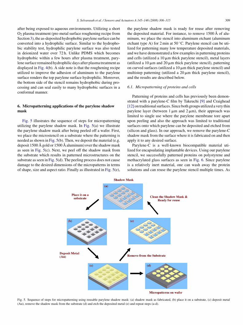
As-deposited parylene-C, similar to PDMS, displaysydrophobic properties with a contact angle of ∼98 ◦C. The as-eposited hydrophobic parylene surface seals extremely well tother hydrophobic surfaces. Furthermore, it does not adhere wello hydrophilic surfaces, a property that is important while usinghe parylene-C as a shadow mask. Accordingly, we have char-cterized the contact angle and the stability of parylene sheetsn aqueous environments over time. We have submersed an as-eposited parylene sheet into deionized water for 3 days (whichay be the case for multiple patterning and rinsing experiments)
s seen in Fig. 4(a). For various applications (such as pattern-ng proteins and cells), one would prefer to have a hydrophilicurface and require that the surface maintains such property
ig. 4. (a) Contact angle measurement of as-deposited parylene-C surfacen aqueous environments up to 3 days. (b) Contact angle measurement ofydrophilic parylene surface in aqueous environments up to 3 days.
Actua
aOScbihldustcc
6m
utwndatsdo
ttmelaa(oma
6
s[plus(sa
l
F(
S. Selvarasah et al. / Sensors and
fter being exposed to aqueous environments. Utilizing a short2 plasma treatment (pre-metal surface roughening recipe fromection 3), the as-deposited hydrophobic parylene surface can beonverted into a hydrophilic surface. Similar to the hydropho-ic stability test, hydrophilic parylene surface was also testedn deionized water over 72 h. Unlike PDMS which becomesydrophobic within a few hours after plasma treatment, pary-ene surface remained hydrophilic days after plasma treatment asisplayed in Fig. 4(b). A side note is that the roughening recipetilized to improve the adhesion of aluminum to the paryleneurface renders the top parylene surface hydrophilic. Moreover,he bottom side of the stencil remains hydrophobic during pro-essing and can seal easily to many hydrophobic surfaces in aonformal manner.
. Micropatterning applications of the parylene shadowask
Fig. 5 illustrates the sequence of steps for micropatterningtilizing the parylene shadow mask. In Fig. 5(a) we illustratehe parylene shadow mask after being peeled off a wafer. First,e place the microstencil on a substrate where the patterning iseeded as shown in Fig. 5(b). Then, we deposit the material (e.g.eposit 1500 A gold or 1500 A aluminum) over the shadow masks seen in Fig. 5(c). Next, we peel off the shadow mask from
he substrate which results in patterned microstructures on theubstrate as seen in Fig. 5(d). The peeling process does not causeamage to the desired dimensions of the micropatterns in termsf shape, size and aspect ratio. Finally as illustrated in Fig. 5(e),smis
ig. 5. Sequence of steps for micropatterning using reusable parylene shadow maskAu), remove the shadow mask from the substrate (d) and etch the deposited metal (e
tors A 145–146 (2008) 306–315 309
he parylene shadow mask is ready for reuse after removinghe deposited material. For instance, to remove 1500 A of alu-
inum, we place the stencil into aluminum etchant (aluminumtchant type A) for 2 min at 50 ◦C. Parylene stencil can be uti-ized for patterning many low temperature deposited materials,nd we have demonstrated a few examples in patterning proteinsnd cells (utilized a 10 �m thick parylene stencil), metal layersutilized a 10 �m and 20 �m thick parylene stencil), patterningn curved surfaces (utilized a 10 �m thick parylene stencil) andultistep patterning (utilized a 20 �m thick parylene stencil),
nd the results are described below.
.1. Micropatterning of proteins and cells
Patterning of proteins and cells has previously been demon-trated with a parylene-C film by Takeuchi [9] and Craighead12] on traditional surfaces. Since both groups utilized a very thinarylene layer (between 1 �m and 2 �m), their approach wasimited to single use where the parylene membrane tore apartpon peeling and also the approach was limited to traditionalurfaces onto which parylene can be deposited and etched fromsilicon and glass). In our approach, we remove the parylene-Chadow mask from the surface where it is fabricated on and thenpply it to any desired surface.
Parylene-C is a well-known biocompatible material uti-ized for encapsulating implantable devices. Using our parylene
tencil, we successfully patterned proteins on polystyrene andethacrylated glass surfaces as seen in Fig. 6. Since parylenes a relatively inert material, one can wash away the proteinolutions and can reuse the parylene stencil multiple times. As
: (a) shadow mask as fabricated, (b) place it on a substrate, (c) deposit metal) and repeat steps (a-d).

310 S. Selvarasah et al. / Sensors and Actuators A 145–146 (2008) 306–315
Fm
spwtdnscwpio
6
mimaAmofhia
Fp
uwsrwagest that there is little pattern degradation or blurring duringdeposition indicating an exceptionally good seal between theparylene film and the silicon substrate.
ig. 6. Fluorescent images of proteins patterned on (a) polystyrene and (b)ethacrylated glass surfaces.
hown in Fig. 7(a), we were able to pattern FITC-labeled BSArotein on a PDMS substrate using the stencil. The patterningas repeated nine times, during which the resolution was main-
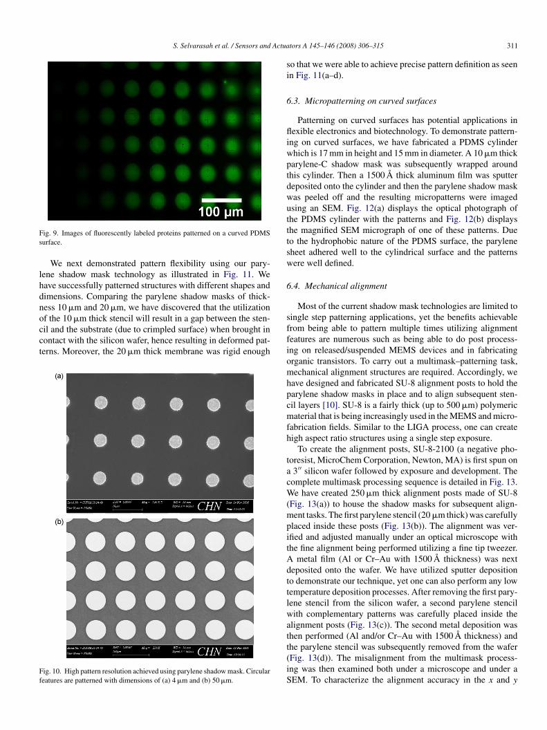
ained as seen in Fig. 7(b). Following protein patterning, we nextemonstrated applications of the parylene stencil in tissue engi-eering and have successfully patterned NIH-3T3 fibroblasts (aseen in Fig. 8) and other cells types including AML12 hepato-ytes and mouse embryonic stem cells on PDMS surfaces. Next,e fabricated a cylindrical PDMS slab and utilizing our flexiblearylene stencil, patterned fluorescently labeled proteins shownn Fig. 9. As illustrated in Fig. 9, due to the flexible nature ofur stencil, one can quite readily pattern curved surfaces.
.2. High pattern resolution and pattern flexibility
To characterize the properties of the parylene-C shadowask, several parylene stencils with various dimensions, spac-
ngs and shapes were fabricated. After fabrication, theseembranes were placed over silicon wafers and metal films (Al
nd Cr–Au) with 1500 A in thickness were sputter deposited.fter the deposition, we have carefully peeled off the shadowask from the silicon wafer and reused it multiple times with-
ut any difficulty. Due to the relatively large dimensions of the
eatures (4–5 �m), one can reuse this mask many times as theoles do not get clogged up and the micropatterns were formedn a reproducible manner. As seen in Fig. 10(a), we were able tochieve fine features as small as 4 �m in a reproducible mannerig. 7. FITC-BSA was patterned on PDMS after (a) 1st patterning and (b) 9thatterning.
sing a 10 �m thick stencil. Utilizing the same shadow mask,e also demonstrated patterning both large and small features
imultaneously as displayed in Fig. 10(b) illustrating the patternesolution of our technology. The feature size measurements thatere conducted using both scanning electron microscope (SEM)
nd the optical microscope agree well with each other and sug-
Fig. 8. Patterned NIH-3T3 fibroblast cells.
S. Selvarasah et al. / Sensors and Actua
Fs
lhdnocct
Ff
si
6
fliwptdwutttsw
6
ig. 9. Images of fluorescently labeled proteins patterned on a curved PDMSurface.
We next demonstrated pattern flexibility using our pary-ene shadow mask technology as illustrated in Fig. 11. Weave successfully patterned structures with different shapes andimensions. Comparing the parylene shadow masks of thick-ess 10 �m and 20 �m, we have discovered that the utilization
f the 10 �m thick stencil will result in a gap between the sten-il and the substrate (due to crimpled surface) when brought inontact with the silicon wafer, hence resulting in deformed pat-erns. Moreover, the 20 �m thick membrane was rigid enoughig. 10. High pattern resolution achieved using parylene shadow mask. Circulareatures are patterned with dimensions of (a) 4 �m and (b) 50 �m.
sffiomhpcmfh
tacW(mpitAdttlwatt(iS
tors A 145–146 (2008) 306–315 311
o that we were able to achieve precise pattern definition as seenn Fig. 11(a–d).
.3. Micropatterning on curved surfaces
Patterning on curved surfaces has potential applications inexible electronics and biotechnology. To demonstrate pattern-
ng on curved surfaces, we have fabricated a PDMS cylinderhich is 17 mm in height and 15 mm in diameter. A 10 �m thickarylene-C shadow mask was subsequently wrapped aroundhis cylinder. Then a 1500 A thick aluminum film was sputtereposited onto the cylinder and then the parylene shadow maskas peeled off and the resulting micropatterns were imagedsing an SEM. Fig. 12(a) displays the optical photograph ofhe PDMS cylinder with the patterns and Fig. 12(b) displayshe magnified SEM micrograph of one of these patterns. Dueo the hydrophobic nature of the PDMS surface, the paryleneheet adhered well to the cylindrical surface and the patternsere well defined.
.4. Mechanical alignment
Most of the current shadow mask technologies are limited toingle step patterning applications, yet the benefits achievablerom being able to pattern multiple times utilizing alignmenteatures are numerous such as being able to do post process-ng on released/suspended MEMS devices and in fabricatingrganic transistors. To carry out a multimask–patterning task,echanical alignment structures are required. Accordingly, we
ave designed and fabricated SU-8 alignment posts to hold thearylene shadow masks in place and to align subsequent sten-il layers [10]. SU-8 is a fairly thick (up to 500 �m) polymericaterial that is being increasingly used in the MEMS and micro-
abrication fields. Similar to the LIGA process, one can createigh aspect ratio structures using a single step exposure.
To create the alignment posts, SU-8-2100 (a negative pho-oresist, MicroChem Corporation, Newton, MA) is first spun on3′′ silicon wafer followed by exposure and development. The
omplete multimask processing sequence is detailed in Fig. 13.e have created 250 �m thick alignment posts made of SU-8
Fig. 13(a)) to house the shadow masks for subsequent align-ent tasks. The first parylene stencil (20 �m thick) was carefully
laced inside these posts (Fig. 13(b)). The alignment was ver-fied and adjusted manually under an optical microscope withhe fine alignment being performed utilizing a fine tip tweezer.
metal film (Al or Cr–Au with 1500 A thickness) was nexteposited onto the wafer. We have utilized sputter depositiono demonstrate our technique, yet one can also perform any lowemperature deposition processes. After removing the first pary-ene stencil from the silicon wafer, a second parylene stencilith complementary patterns was carefully placed inside the
lignment posts (Fig. 13(c)). The second metal deposition washen performed (Al and/or Cr–Au with 1500 A thickness) and
he parylene stencil was subsequently removed from the waferFig. 13(d)). The misalignment from the multimask process-ng was then examined both under a microscope and under aEM. To characterize the alignment accuracy in the x and y
312 S. Selvarasah et al. / Sensors and Actuators A 145–146 (2008) 306–315
Fig. 11. High pattern flexibility: (a) the width of the spiral is 100 �m, (b) the smallest anbetween squares is 15 �m, (c) starfish patterns, (d) the rectangular patterns where the
Fig. 12. Micropatterning on curved surfaces: (a) optical image of the PDMScylinder with micropatterns and (b) magnified SEM micrograph of one of thepatterns.
dstxty
wtt1
Ftpo
d the biggest squares are 10 �m × 10 �m and 100 �m × 100 �m and the spacingspacing between lines is 15 �m and the width of an individual line is 25 �m.
irections, we have created two different complementary “E-haped” structures [10,19] as seen in Fig. 14. Fig. 15 displayshe measurements from the alignment tests. In the x-direction, an-offset of 4.6 �m and y-offset of 8.6 �m were measured usinghe complementary structures. In the y-direction, the x-offset and-offset were 6.9 �m and 4.1 �m, respectively.
In summary, we demonstrated a multistep patterning process
ith a misalignment of about 4–9 �m using SU-8 pillars. Duringhese experiments, we have utilized two different thicknesses forhe SU-8 posts (100 �m and 250 �m). We have found out that the00 �m posts did not hold the parylene shadow masks properly
ig. 13. Micropatterning using SU-8 alignment pillars: (a) fabricate 250 �mhick SU-8 pillars, (b) place the first shadow mask, (c) deposit metal and theneel off the first shadow mask and place the second shadow mask, and (d) peelff the second shadow mask.

S. Selvarasah et al. / Sensors and Actua
Fig. 14. Test structures for misalignment measurements in x and y directionswhere the width of the electrode is 10 �m and the spacing between themis 50 �m: (a) alignment tests in x-direction using complementary ‘E’ shapedstructures and (b) alignment test in y-direction using the same structures.
Fig. 15. Measured offsets from the misalignment measurements in x (a) and y(b) directions.
dta
cisidilaitttfl
7
postapdgcpPit4flclwCfiib
A
F00
R
tors A 145–146 (2008) 306–315 313
uring manual manipulation (for minor adjustments) whereashe thicker version (250 �m) holds the shadow mask in placend hence was the alignment post of choice.
Among its many advantages, parylene shadow masks can beleaned and are resuable (for at least 10 times) since parylenes an inert material [20]. The fabrication technology is fairlyimple, even though we demonstrated our stencils on three-nch wafers, one can easily extend this technology to largerimensions. Furthermore, due to its mechanical strength andts reusability, one can utilize this technology for patterningarge area devices in Flextronics and Macroelectronics as wells patterning for heterogeneous device integration. A final notes that a thin parylene membrane (<10 �m) has the tendencyo fold while being held by tweezers, which makes it difficulto precisely position the shadow mask on the sample. Thus, ahicker membrane of at least 20 �m is required for high patternexibility and for large area patterning applications.
. Conclusions
In this paper, we present a flexible, reusable, biocompatiblearylene-C shadow mask technology. The minimum feature sizef 4 �m is demonstrated while using a 10 �m thick parylene-Ctencil for small area patterning applications. A low tempera-ure (5 ◦C) high aspect ratio (>8:1) parylene etch process waslso developed to fabricate the fine structures with anisotropicrofiles. Utilizing this flexible shadow mask technology, weemonstrated patterning of proteins and cells on polystyrene,lass and PDMS surfaces. The parylene shadow mask is bio-ompatible, chemically inert and reusable. Micropatterning ofroteins as well as inorganic materials (metals) on curvedDMS surfaces are also demonstrated. Multimask processing
s demonstrated with the addition of SU-8 support pillars andhe misalignment between masks was measured to be between�m and 9 �m. The parylene stencil method has high patternexibility as various shapes with different dimensions can bereated utilizing the same stencil. The thickness of the pary-ene stencil is critical for large area micropatterning applicationshere a 20 �m thick stencil needs to be utilized. The parylene-shadow mask technology is versatile and will potentially
nd diverse patterning applications in numerous fields includ-ng organic electronics, macroelectronics, metamaterials andiotechnology.
cknowledgments
The authors would like to thank for the support by the Airorce Research laboratory, Hanscom, MA, contract # FA8718-6-C-0045 and the National Science Foundation (Award NSF-425826 and Award NER-0608892).
eferences
[1] C.G. Courcimault, M.G. Allen, Reconfigurable shadow mask technology:a microsystem for metal nanoline deposition, Nanotechnology 15 (2004)S528–S533.

3 Actua
[
[
[
[
[
[
[
[
[
[
[
[
B
SfwiiFR
SCUCA
CicNam
SgUIbfn2hNpffooeNr
Aotaimfdt2cpceoNtSCEWat
14 S. Selvarasah et al. / Sensors and
[2] R. Luethi, R.R. Schlittler, J. Brugger, P. Vettiger, M.E. Welland, J.K.Gimzewski, Parallel nanodevice fabrication using a combination of shadowmask and scanning probe methods, Appl. Phys. Lett. 75 (1999) 1314–1316.
[3] M. Graff, S.K. Mohanty, E. Moss, A.B. Frazier, Microstencilling: a generictechnology for microscale patterning of vapor deposited materials, JMEMS13 (2004) 956–962.
[4] C.C. Tseng, C.W. Chiu, K.X. Zhung, J.H. Lee, G.D.J. Su, Thin siliconshadow masks for organic light emitting diodes (OLED) deposition pro-cesses, Proc. SPIE 6414 (2007) 64141G.
[5] S.M. Yi, S.H. Jin, J.D. Lee, C.N. Chu, Fabrication of high-aspect-ratiostainless-steel shadow mask and its application to pentacene thin-film tran-sistors, J. Micromech. Microeng. 15 (2) (2005) 263–269.
[6] A. Tixier, Y. Mita, J.P. Gouy, H. Fujita, A silicon shadow mask for depo-sition on isolated areas, J. Micromech. Microeng. 10 (2) (2000) 157–162.
[7] G.M. Kim, M.A.F. van den Boogaart, J. Brugger, Fabrication and applica-tion of a full wafer size micro/nanostencil for multiple length-scale surfacepatterning, Microelectron. Eng. 67/68 (2003) 609–614.
[8] H.J. Fan, F. Fleischer, W. Lee, K. Nielsch, R. Scholz, M. Zacharias, U.Gosele, A. Dadgar, A. Krost, Patterned growth of aligned ZnO nanowirearrays on saphire and GaN layers, Superlattices Microstruct. 36 (2004)95–105.
[9] K. Atsuta, H. Noji, S. Takeuchi, Micropatterning of active proteinswith perforated PDMS sheets (PDMS Sieve), Lab Chip 4 (2004) 333–336.
10] G. Kim, B. Kim, J. Brugger, All-photoplastic microstencil with self-alignment for multiple layer shadow-mask patterning, Sens. Actuators A107 (2003) 132–136.
11] F.-G. Tseng, C.-L. Yu, High aspect ratio ultrathick micro-stencil by JSRTHB-430N negative UV photoresist, Sens. Actuators A 97/98 (2002)764–770.
12] B. Ilic, H.G. Craighead, Topographical patterning of chemically sensitivebiological materials using a polymer-based dry lift off, Biomed. Microde-vices 2 (2000) 317–322.
13] S. Selvarasah, P. Makaram, C.-L. Chen, X. Xiong, S.-H. Chao, A. Bus-naina, S. Sridhar, M.R. Dokmeci, A three dimensional multi-walled carbonnanotube based thermal sensor on a flexible parylene substrate, IEEE Nan-otechnol., Hong Kong, China, August 2–5, 2007.
14] C.-L. Chen, S. Selvarasah, S.-H. Chao, A. Khanicheh, C. Mavroidis, M.R.Dokmeci, Electrohydrodynamic micropump for on chip fluid pumping onflexible parylene substrates, in: Proceedings of the IEEE NEMS Confer-ence, Bangkok, Thailand, 2007, pp. 826–829.
15] J.B. Fortin, T.-M. Lu, Chemical Vapor Deposition Polymerization—theGrowth and Properties of Parylene Thin Films, Kluwer Academic Publish-ers, Boston, 2004.
16] B. Ilic, D. Czaplewski, M. Zalalutdinov, B. Schmidt, H.G. Craighead, Fab-rication of flexible polymer tubes for micro and nanofluidic applications,J. Vac. Sci. Tech. B (2002) 2459–2465.
17] L. Marty, A. Bonhomme, A. Iaia, E. Andre, E. Rauwel, C. Duboudieu,A. Toffoli, F. Ducroquet, A.M. Bonnot, V. Bouchiat, Integration of self-assembled carbon nanotube transistors: statistics and gate engineering atthe wafer scale, Nanotechnology 17 (2006) 5038–5045.
18] E. Meng, S. Aoyagi, Y.C. Tai, High aspect ratio parylene etching formicrofluidics and BioMEMS, in: Proceedings of the MicroTAS’04, vol.2, Malmo, Sweden, 2004, pp. 401–403.
19] A. Ludwig, J. Cao, J. Brugger, I. Takeuchi, MEMS tools for combina-tional materials processing and high-throughput characterization, Meas.Sci. Technol. 16 (2005) 111–118.
20] S. Selvarasah, S.-H. Chao, C.-L. Chen, D. Mao, J. Hopwood, S. Ryley,S. Sridhar, A. Khademhosseini, A. Busnaina, M.R. Dokmeci, A highaspect ratio, flexible, transparent and low-cost parylene-C shadow masktechnology for micropatterning applications, in: Proceedings of the Trans-
ducers’07, Lyon, France, 2007, pp. 533–536.21] D. Wright, B. Rajalingam, J.M. Karp, S. Selvarasah, Y. Ling, J. Yeh, R.Langer, M.R. Dokmeci, A. Khademhosseini, Reusable, reversibly sealableparylene membranes for cell and protein patterning, J. Biomed. Mater. Res.A 85 (2007) 530–538.
e
Aaa
tors A 145–146 (2008) 306–315
iographies
elvapraba Selvarasah received his BSc, degree in Computer Engineeringrom McMaster University, Hamilton, Ontario, Canada, in 2002. He is currentlyorking towards his PhD degree in the Electrical and Computer Engineer-
ng Department at Northeastern University, Boston, MA. His research interestsnclude Photonic Crystals, Flexible Electronics, Nanoscale Integration, Organicield Effect Transistors, and BioMEMS. He is a member of the Materialsesearch Society.
hih-Hsieh Chao is currently pursuing his MS degree in the Electrical andomputer Engineering Department at Northeastern University, Boston, MA,SA. He received his BS degree in Electronic Engineering from Chung Yuanhristian University in 2004. His research interests include Dielectrophoreticssembly of Nanomaterials and Nanomaterials based devices.
hia-Ling Chen received her Master of Science degree in Electrical Engineer-ng from National Taiwan University (NTU), Taipei, Taiwan, in 2003. She isurrently pursuing her PhD degree in the Electrical and Computer Engineering atortheastern University, MA, USA. Her research interests include nano-material
ssembly, Nanofabrication, Microfluidics, and Flexible Electronics. She is aember of the IEEE and the Materials Research Society.
rinivas Sridhar is Vice Provost for Research, and Arts and Sciences Distin-uished Professor and Chairperson in the Physics Department at Northeasternniversity. He is the Director of Nanomedicine Science and Technology, an
GERT (Integrative Graduate Education and Research Training) program fundedy the National Cancer Institute and the National Science Foundation. He is theounding director of the Electronic Materials Research Institute and a leadinganomedicine and nanophotonics researcher. His paper published in Nature in003 was selected among the Breakthroughs of 2003 by the journal science. Heas published more than 130 journal articles in prestigious journals includingature, Physical Review Letters, Applied Physics Letters, and others. He hasresented more than 180 invited talks in 15 countries, co-organized 10 con-erences and co-edited two conference proceedings. He has served as refereeor 12 professional journals and is a frequent proposal reviewer for federal andther funding agencies, including the National Science Foundation, Departmentf Energy, Department of Defense, American Chemical Society and many oth-rs. As Vice Provost for Research, Professor Sridhar administers and promotesortheastern University’s research program, and develops new inter-disciplinary
esearch and education programs and clusters of excellence.
.A. Busnaina, PhD is the William Lincoln Smith Chair Professor and Directorf National Science Foundation’s Nanoscale Science and Engineering Cen-er (NSEC) for high-rate nanomanufacturing and the NSF Center for Nanond Microcontamination Control at Northeastern University, Boston, MA. Hes internationally recognized for his work on nano- and micro-scale defectsitigation and removal in semiconductor fabrication. He also involved in the
abrication of nano-scale wires, structures and interconnects. He specializes inirected assembly of nanoelements (such as nanotubes and nanoparticles) and inhe fabrication of micro- and nano-scale structures. Research support exceeded5 million dollars. He served as a consultant on microcontamination and parti-le adhesion issues to the semiconductor industry. He authored more than 300apers in journals, proceedings and conferences. He organized more than 80onferences, workshops, symposia and programs for many professional soci-ties, chaired and organized more than 90 sessions and panels. He also servesn many advisory boards including Samsung Electronics; Chemical Industryanomaterials Roadmap, International Technology Roadmap for Semiconduc-
ors, Journal of Particulate Science and Technology, Journal of Environmentalciences, Semiconductor International, Journal of Advanced Applications inontamination Control. He is a fellow of the American Society of Mechanicalngineers, and the Adhesion Society, a Fulbright Senior Scholar and listed inho’s Who in the World, in America, in science and engineering, etc.). He was
warded the 2006 Nanotech Briefs National Nano50 Award, Innovator category,he 2006 Outstanding Faculty, SØren Buus Outstanding Research Award, North-
astern University 2006, the 2005 Aspiration Award, Northeastern University.li Khademhosseini is an Assistant Professor of Medicine and Health Sciencesnd Technology at Harvard-MIT’s Division of Health Sciences and Technologynd the Harvard Medical School. His research is based on developing micro-

Actua
ase8iRGosPd
MU
ohsDhphHW
S. Selvarasah et al. / Sensors and
nd nano-scale technologies to control cellular behavior with particular empha-is in developing microscale biomaterials and engineering systems for tissuengineering and drug delivery. He has published over 70 peer reviewed papers,0 abstracts and 14 issued or pending patents. He has received multiple awardsncluding the TR35 awarded to the top Young Innovators by the Technologyeview Magazine (2007), the Coulter Foundation Early Career (2006), BMWroup Scientific Award (2007), outstanding research mentor at MIT (2004),utstanding researcher in polymer science by OMNOVA/MIT (2005) and out-tanding research by Biomedical Engineering Society (2005). He received his
hD in bioengineering from MIT (2005), and MASc (2001) and BASc (1999)egrees from University of Toronto both in chemical engineering.ehmet R. Dokmeci received BS (with distinction) and MS degrees from theniversity of Minnesota, Minneapolis and the PhD degree from the University
aodsD
tors A 145–146 (2008) 306–315 315
f Michigan, Ann Arbor, all in electrical engineering. His dissertation was onermetic encapsulation of implantable microsystems for chronic use in livingystems. Since Fall 2004, he is with the Electrical and Computer Engineeringepartment at Northeastern University as an Assistant Professor. Previously,e was an Assistant Research Scientist in the Electrical Engineering and Com-uter Science Department at the University of Michigan, Ann Arbor, wheree developed a Pb–Sn solder-based wafer level vacuum packaging technology.e has 3.5 years of industrial experience at Corning-Intellisense Corporation,ilmington, MA developing MEMS-based products for the telecommunications
nd life sciences industries. His research interests are concentrated in all areasf micro- and nanomachining and its applications to biomedical and opticalevices, Nano-scale integration, flexible electronics, and implantable biosen-ors. He has authored and co-authored 42 technical publications in these areas.r. Dokmeci is a member of IEEE, SEM, ACS, and MRS.