a radiation-hard pll for frequency multiplication with programmable input clock and phase-selectable...
TRANSCRIPT

A Radiation-Hard PLL for Frequency Multiplication with Programmable Input Clock and Phase-Selectable Output Signals in 130 nm CMOS
Filip TavernierKarolina PoltorakSandro BonaciniPaulo Moreira

Filip Tavernier - CERN 2
Outline
• Introduction• ePLL topology• ePLL design aspects• Measurement results

Filip Tavernier - CERN 3
The bigger picture
On-DetectorCustom Electronics & Packaging
Radiation Hard
Off-DetectorCommercial Off-The-Shelf (COTS)
Custom Protocol
Development of a high-speed bidirectional optical link for the LHC experiments upgrade program:• Versatile link project: opto-electronics• GBT project: ASIC design, especially for on-detector systems

Filip Tavernier - CERN 4
The GBT system
FEModule
FEModule
Phase – Aligners + Ser/Des for E – Ports
FEModule
E – PortE – Port
E – Port
GBT – SCA
E – Port
Phase - Shifter
E – PortE – Port
E – PortE – Port
CDR
DEC/D
SCR
SER
SCR/ENC
I2C MasterI2C Slave
Control Logic Configuration(e-Fuses + reg-Bank)
Clock[7:0]
CLK Manager
CLK Reference/xPLL
External clock reference
clockscontroldata
one 80 Mb/s port
I2C port
I2C (light)
JTAG
80, 160 and 320 Mb/s ports
GBTIA
GBLD
GBTXe-Link
clock
data-up
data-downePLLTx
ePLLRx
JTAG port
Filip Tavernier - CERN 5
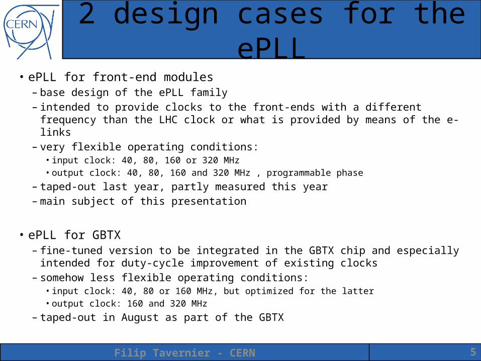
2 design cases for the ePLL• ePLL for front-end modules
– base design of the ePLL family– intended to provide clocks to the front-ends with a different frequency than the LHC
clock or what is provided by means of the e-links– very flexible operating conditions:
• input clock: 40, 80, 160 or 320 MHz• output clock: 40, 80, 160 and 320 MHz , programmable phase
– taped-out last year, partly measured this year– main subject of this presentation
• ePLL for GBTX– fine-tuned version to be integrated in the GBTX chip and especially intended for
duty-cycle improvement of existing clocks– somehow less flexible operating conditions:
• input clock: 40, 80 or 160 MHz, but optimized for the latter• output clock: 160 and 320 MHz
– taped-out in August as part of the GBTX

Filip Tavernier - CERN 6
Outline
• Introduction• ePLL topology• ePLL design aspects• Measurement results

Filip Tavernier - CERN 7
VCO320 MHz
337.5°
0°22.5°45°LPFCPPFDinput
divider
feedbackdivider
inputclock
320 MHz
80 M
Hz
160
MH
z
40 M
Hz
0°, 90°, 180°, 270°
ePLL topology (1)
• input divider: programmable divider ratio so that the output is always 40 MHz• feedback divider: fixed divider ratio of 8 because the VCO runs at 320 MHz• PFD: determines the frequency and phase difference between the 40 MHz input
clocks and outputs UP and DOWN signals which are linearly dependent on the phase difference

Filip Tavernier - CERN 8
VCO320 MHz
337.5°
0°22.5°45°LPFCPPFDinput
divider
feedbackdivider
inputclock
320 MHz
80 M
Hz
160
MH
z
40 M
Hz
0°, 90°, 180°, 270°
ePLL topology (2)
• CP: charge pump with a 6-bit programmable output current to convert the UP and DOWN signals of the PFD to the current domain• LPF: 1st order loop filter referred to the supply voltage because of the pMOS
current sources in the VCO• VCO: voltage-controlled ring-oscillator at 320 MHz with 16 output phases

Filip Tavernier - CERN 9
Outline
• Introduction• ePLL topology• ePLL design aspects• Measurement results

Filip Tavernier - CERN 10
Phase-frequency detector
edgedetector
edgedetector
feedbackclock
inputclock
late
early
rese
t
inputclock
feedbackclock
late
early
• linear relationship between the duration of the early/late pulses and the phase error• PFD is sensitive to phase and frequency errors which leads to a PLL with a locking
range that is basically limited by the VCO tuning range• delay of the NOR gate results in the early/late pulses go high every clock cycle → ‘4’
possible output states of the PFD• ‘translation’ of signals taking into account the pMOS current source in the VCO
early → VCO is too fast → DOWN → source current into the loop filterlate → VCO is too slow → UP → sink current from the loop filter

Filip Tavernier - CERN 11
Charge pump (1)
DAC
1:1
1:1
1:1
down
up
down
up
Iout
_up
_down
_up
_down
UP = low and DOWN = lowno current flows to the loop filter or in the unity-gain amplifierUP = high and DOWN = highno current flows to the loop filter if sink and source currents are equal!

Filip Tavernier - CERN 12
Charge pump (2)
DAC
1:1
1:1
1:1
down
up
down
up
Iout
_up
_down
_up
_down
UP = high and DOWN = lowsink current flows out of the loop filter, source current flows into the amplifierUP = low and DOWN = highsource current flows into the loop filter, sink current flows out of the amplifier

Filip Tavernier - CERN 13
Charge pump non-idealities• unequal sink and source currents
The loop filter is charged or discharged by the current difference when UP and DOWN are both high every clock cycle. → static phase error→ solution: current sources with long length and consequently high output impedance
• parasitic capacitance at the drain of the current sourcesCharge sharing takes place every time one of the current sources is connected to the loop filter→ static phase error→ solution: unity-gain amplifier to equalize the drain voltage of the current sources to the control voltage

Filip Tavernier - CERN 14
D2S D2S
202.
5°
22.5
°
180°0°
D2S
225°45
°
D2S
247.
5°
67.5
°
D2S
270°90
°
D2S
292.
5°
112.
5°
D2S
315°
135°
D2S
337.
5°
157.
5°
Voltage-controlled oscillator
• 8-stage differential ring-oscillator• 8 D2S converters to generate the full-swing output phases (0°, 22.5°, 45°, 67.5°,
90°, 112.5°, 135°, 157.5°) from the analog levels in between the delay stages• inverters used to generate the other 8 phases to save the power of another 8 D2S
converters• transmission gates to equalize the phases generated by the D2S converters
directly and the ones generated by the inverters

Filip Tavernier - CERN 15
VCO – delay cell
• pMOS differential pair with pMOS current source → control voltage referred to the supply voltage
• input transistors biased with small overdrive voltage because of the relatively large cell delay of 195.3125 ps
• active load consisting of a current source and a diode to avoid the need for a common-mode feedback circuit and still have enough small-signal gain
• gate voltage of the nMOS current sources derived by means of a replica biasing circuit

Filip Tavernier - CERN 16
Radiation hardness (1)• total ionizing dose
– all transistors have a gate width of at least 1 µm → no leakage– 130 nm CMOS is generally known for its good TID radiation hardness
• single-event upsetsVCO is most critical because it can take a long time to recover after an SEU → simulated with current injected in 3 sensitive nodes
I1
I2
I3

Filip Tavernier - CERN 17
Radiation hardness (2)
maximum phase error of 533 ps(current I3, 0.3 pC in 10 ps)
↓loop corrects this in ± 2 clock cycles

Filip Tavernier - CERN 18
Outline
• Introduction• ePLL topology• ePLL design aspects• Measurement results

Filip Tavernier - CERN 19
Some numbers
1 D2S 29 mW1 extra D2S 30.5 mWAll D2S 41.5 mW
• 130 nm CMOS• size of the test chip: 2 mm x 1 mm• size of the core circuit: 385 µm x 325 µm

Filip Tavernier - CERN 20
Measurement of the output phases (1)

Filip Tavernier - CERN 21
Measurement of the output phases (2)
If needed, the 40, 80 and 160 MHz output clocks can be resampled with any of the320 MHz output phases in order to increase the phase resolution to 22.5°.

Filip Tavernier - CERN 22
Measurement of the output jitter (1)
jitter values < 10 psRMS are possible

Filip Tavernier - CERN 23
Measurement of the output jitter (2)
jitter values < 10 psRMS are possible

Filip Tavernier - CERN 24
Measurement of the jitter transfer

Filip Tavernier - CERN 25
Conclusions
• a highly flexible ePLL has been presented• programmable input clock frequency of 40, 80, 160 or
320 MHz• output clocks of 40, 80, 160 or 320 MHz are always
available• output phase can be programmed with a resolution of
90° for the 40, 80 and 160 MHz outputs and 22.5° for the 320 MHz output
• measurements have shown a good jitter performance