a process-tolerant low-power adder architecture for image
TRANSCRIPT

Turk J Elec Eng & Comp Sci(2019) 27: 1839 – 1854© TÜBİTAKdoi:10.3906/elk-1809-8
Turkish Journal of Electrical Engineering & Computer Sciences
http :// journa l s . tub i tak .gov . t r/e lektr ik/
Research Article
A process-tolerant low-power adder architecture for image processing applications
Bharat GARG1,∗ , G. K. SHARMA2
1Electronics and Communication Engineering, Faculty of Engineering, Thapar University, Patiala, India2ABV-Indian Institute of Information Technology and Management Gwalior, India
Received: 02.09.2018 • Accepted/Published Online: 06.01.2019 • Final Version: 15.05.2019
Abstract: The aggressive CMOS technology scaling in the sub-100-nm regime leads to highly challenging VLSI designdue to the presence of unreliable components. The delay failures in arithmetic units are increasing rapidly due to theincreased effect of process variation (PV) in scaled technology. This paper introduces a novel process-tolerant low-power adder (Prot-LA) architecture for error-tolerant applications. The proposed Prot-LA architecture segments theoperands into two parts and computes addition of the upper parts in carry-propagate, whereas it computes the lowerparts in a carry-free manner. In the Prot-LA, the number of bits in carry-propagate and carry-free additions can bereconfigured based on the amount of PV. An on-chip PV detector is embedded to determine the PV severity. Becauseof this reconfigurability, the proposed adder completes the carry propagation with minimum error even under severeprocess variation. The simulation results show that proposed Prot-LA provides 19.9% reduced power consumption overthe state-of-the-art approximate adder. The efficacy of the proposed adder is demonstrated in the real application bydesigning an image scaling processor (ISP). The simulation results show that the Prot-LA embedded ISP consumes 7.75%reduced energy with 2.43 dB higher PSNR over the existing approximate adder embedded ISP.
Key words: Low power, approximate designs, process variation, error-resiliency, image scaler
1. IntroductionThe rapid development of the VLSI technology has lead to an exponential growth of portable electronic devicesthat employ several applications to satisfy user demand. Low power is the inherent requirement of all portabledevices to extend the battery lifetime, improve reliability, and reduce the cost associated with heat removal.Scaling is no more the solution to address these challenges due to the increased effect of process variation(PV). The intra-die PV exhibits random behavior and may increase or decrease the delay. The die where largecomputations take place to evaluate the ultimate result, the overall delay comes out to the average value whichmay not be significant. Therefore, most of the existing techniques try to mitigate inter-die PV due to havingsystematic behavior. The PV-induced delay spread is almost 30% at 70-nm technology and raises to more than50% at 45-nm technology [1, 2], which reduces the yield of the chip significantly. The logic required to mitigatethe effect of PV is becoming more costly in terms of area, power, and performance. Therefore, there is a growingneed for designs that jointly address the process variation effect and low power requirement.
There are numerous applications that do not demand exact computations while processing the inputdata i.e. these applications can accept certain amount of error. The relaxation of computational accuracy inthese applications is due to the limited perception of human vision, existence of redundancy in input data, and∗Correspondence: [email protected]
This work is licensed under a Creative Commons Attribution 4.0 International License.1839

GARG and SHARMA/Turk J Elec Eng & Comp Sci
nonexistence of accurate output. These applications include image/video processing, artificial neural networks,etc. and are commonly known as error-tolerant applications. The conventional design approaches that performaccurate computations become inefficient designs for these applications. The approximate designs reduce powerconsumption while exhibiting acceptable error in output such that overall quality is maintained. Since additionis the fundamental operation that is used in the computations, the design of process-tolerant low-power adderis the critical requirement.
This paper presents a novel process-tolerant low-power adder architecture that jointly addresses thetechnology issue and provides improved speed-power-accuracy-area trade-off. The major contributions of thepaper are:
1. A novel algorithm and architecture of reconfigurable carry-propagate adder (RCPA) is proposed that candynamically change the number of bits to be added with/without carry propagation.
2. Proposed a novel full adder circuit that can compute accurate/approximate sum based on the controlsignal.
3. A novel process-tolerant adder architecture is proposed that can detect process severity and can configurethe number bits which will be added accurately without timing failure.
4. Finally, the paper demonstrates improved performance of the proposed adder over the state-of-the-artadder architectures in the image scaling processor.
The rest of the paper is organized as follows: Section 2 explores various approximate adder architecturesthat exhibit performance-quality trade-off. A novel process-tolerant adder architecture is presented in Section3 while the analysis of PV severity is presented in Section 4. Section 5 first evaluates and compares theperformance of the proposed adder over the existing architectures as a standalone arithmetic unit and thenevaluates its efficacy in the image processing application. Finally, the work is concluded in Section 6.
2. Literature reviewThe last few decades show a healthy competition between researchers to develop designs for the energy/power-efficient VLSI chips. All these designs exhibit trade-off in different design metrics such as area, power, anddelay. To further improve the performance of these designs, the concept of approximate computing is utilizedwhich provides acceptable results besides underlying some incorrect computations. Thus, accuracy acts as a newtrade-off parameter for these applications and provides improved performance/energy-efficiency at the cost ofaccuracy/quality [3, 4]. The conventional approaches exploit truncation, overclocking, and voltage overscalingto achieve improved performance in different error-resilient applications [5].
Along with the design of high performance signal processing units via approximate architectures and/oralgorithms, low power high performance approximate arithmetic units, such as adders and multipliers have alsobeen proposed via the concept of shortening the critical-path. In the direction of designing adder with reducedcarry propagation path, Zhu et al. [6–9] introduced four approximate error-tolerant adders (ETA) namely:ETA-I, ETA-II, ETA-IIM, and ETA IV. In ETA-I [6], input operands are segmented into accurate parts whichconsist of few most significant bits (MSB) and inaccurate parts which consist of the remaining least significantbits (LSB) to achieve approximate results. ETA-II [8] design cuts the carry propagation to increase the speedof the adder at the cost of large error at MSBs. ETA-IIM is the modified version of ETA-II where more MSBs
1840

GARG and SHARMA/Turk J Elec Eng & Comp Sci
are connected through carry-chain to reduce the error. ETA-IV overcomes the short-comings of ETA-II andETA-IIM by considering high-speed carry-select adder for MSB addition. Further, Shin et al. [10] introduced adata path redesign technique for various adders where the critical path of the carry-chain is curtailed. The logiccomplexity reduction approach at transistor level is reported in [11] to achieve various imprecise full addersand the efficacy of these approximate adders is demonstrated in the image/video compression algorithms. Kaiet al. [12] used a new function speculation technique for designing latency speculative adders. Mazahir etal. presented an area-efficient error correction circuit for the approximate designs [13]. Recently, approximatereverse carry-propagate adder architecture is presented in which carry propagates in a counter-flow manner [14].The RCPA reduces timing variation-induced large errors at the cost of fixed design-specific error.
Along with approximate designs/architectures, different approximate design methodologies/synthesis ap-proaches have also been introduced [15–17]. Huang et al. [15] presented a general methodology for fidelity-efficiency design space exploration and implemented imprecise adders in CORDIC algorithm at 130-nm technol-ogy. A design methodology for reducing power consumption using approximate arithmetic unit cells is presentedin [16]. Further, Lee et al. [17] presented a high-level synthesis tool that exploits arithmetic unit precision andvoltage scaling to reduce energy consumption while maintaining the quality constraint. Finally, Rahimi et al.[18] presented variability-aware OpenMP environment using shared, variation-tolerant, and accuracy reconfig-urable floating point units.
Although the fixed accuracy design techniques discussed above provide improved performance, theirscope is limited due to the different accuracy requirement in different applications. To achieve desirableaccuracy, Kahng et al. [19] demonstrated an accuracy configurable adder (ACA) where accuracy of theresults can be configured during runtime to achieve desired throughput and power efficiency. In the genericaccuracy configurable (GeAr) [20], error correction is implemented by changing the inputs to the subadders andreevaluating the partial sums. An iterative accuracy programmable adder that can reconfigure the probabilityof getting correct output was proposed in [21]. Recently, a reconfigurable carry–look-ahead adder (RCLA)[22] has been presented in which longest carry propagation path is truncated when operated in approximatemode. Since the RCLA exhibits on two operating modes (accurate/approximate), the design must have moreapproximate modes with different accuracy-performance trade-off for large applicability.
All these aforementioned techniques exploit error tolerance of the application and compute the approx-imate output. In the nano-scaled design, the effect of process variation is intolerable and cannot be ignored.Therefore, an arithmetic unit that provides process variation tolerance along with the trade-off between qualityand performance is highly desirable. The adder architecture proposed in the next section provides acceptableoutput even under severe process environment.
3. Proposed process-tolerant low-power adder (Prot-LA) architecture
This section begins with the architecture of the proposed Prot-LA followed by the algorithm and microarchi-tectures of its various parts.
3.1. Prot-LA architectureIn the worst case, the PV-induced delay variation may cause delay of the adder to be twice the original delay.In this case, half of the carry propagation will be done correctly. If delay variation is less than the worst case,more carry propagation can be considered to compute the sum. Therefore, in the proposed addition approach,
1841

GARG and SHARMA/Turk J Elec Eng & Comp Sci
the operands are divided into two parts: the upper part which consists of some most significant bits (MSB) andthe lower part which consists of the remaining least significant bits (LSB). The architecture of the Prot-LA,as shown in Figure 1, consists of conventional accurate adder for MSBs addition, a reconfigurable adder forcarry-propagate/carry-free addition of LSBs, controller, and PV detection logic. In the proposed adder, PVdetection logic determines the PV severity which is given to the controller to generate a control signal. TheProt-LA reconfigures the lower adder to compute sum either in carry-propagate (accurate) or in carry-free(approximate) manner based on the value of control signal. As the PV severity increases, the control signalreduces (increases) the number of carry-propagate (carry-free) bits to compute the sum which reduces the largeerror at MSBs. The next subsection details the architecture and working reconfigurable lower part adder i.e.reconfigurable carry-propagate adder.
logicPV detection
Controlsignal
Decoder
Reconfigurable CarryPropagate Adder
Conventional Adder
Cout
AH BH AL BL
A B
S LH S
S
Figure 1. Architecture of the proposed adder.
3.2. Reconfigurable carry propagation adder: algorithm and architecture
In the Prot-LA, the addition of the least significant bits is done by reconfigurable carry propagation adder whichcomputes addition accurately (carry-propagate)/approximately (carry-free) based on the given control signal.The algorithm 1 provides various steps to compute the approximate sum of operands A and B for the givencontrol signal (CTL). The control signal exhibits maximally one bit at logic ‘1 ’ and other bits are set to logic‘0 ’. All bits of control at logic ‘0 ’ reflects no PV effect. Further, if the higher bit of the CTL is ‘1 ’, it reflectslarge PV. The algorithm first computes the operand part for which accurate sum is to be calculated for a givenCTL. For the rest of the lower bits, the corresponding sum bits are approximated to 1’s. If all the bits of CTLare ‘0 ’, the result of the sum will be accurate.
Algorithm 1 RCPA(A,B,CTL)Inputs: A : Augend,
B : Addend,CTL : Control bits
Output: Sum ≈ A+B
AH ← floor(A/2CTL );BH ← floor(B/2CTL ); ▷ Compute upper partSumH ← AH +BH ; ▷ Compute accurate sumSumL ← 2CTL − 1 ; ▷ Compute approximate sumSum← SumH × 2CTL + SumL ; ▷ Compute final sum
Return Sum ▷ Return accurate/approximate sum
1842
GARG and SHARMA/Turk J Elec Eng & Comp Sci
MFAMFA MFA MFA
S0
SSS 1N−2N−1
A B A B001 1BN−2AN−2N−1BN−1A
Controller
outC
Sum Generator
CTLN−1
CTL N−2 CTL1 CTL0
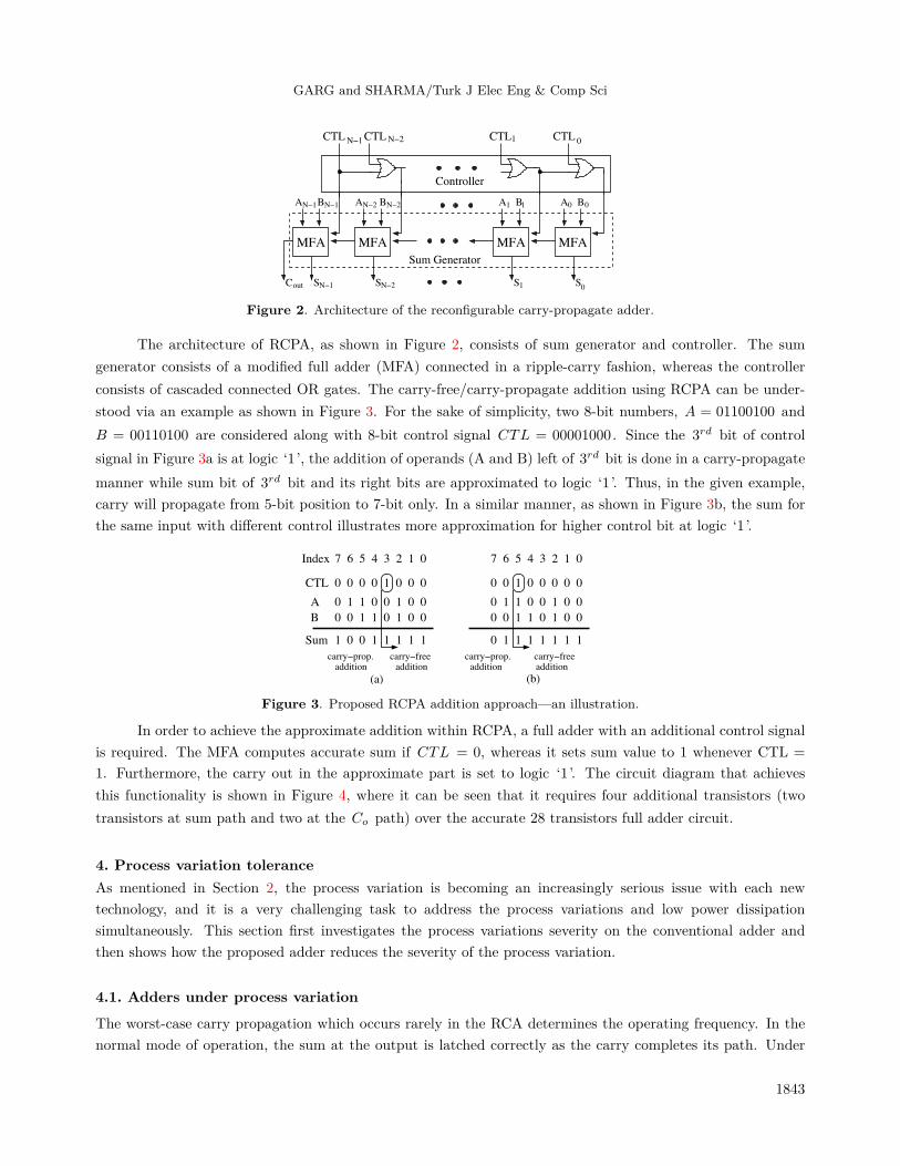
Figure 2. Architecture of the reconfigurable carry-propagate adder.
The architecture of RCPA, as shown in Figure 2, consists of sum generator and controller. The sumgenerator consists of a modified full adder (MFA) connected in a ripple-carry fashion, whereas the controllerconsists of cascaded connected OR gates. The carry-free/carry-propagate addition using RCPA can be under-stood via an example as shown in Figure 3. For the sake of simplicity, two 8-bit numbers, A = 01100100 andB = 00110100 are considered along with 8-bit control signal CTL = 00001000 . Since the 3rd bit of controlsignal in Figure 3a is at logic ‘1 ’, the addition of operands (A and B) left of 3rd bit is done in a carry-propagatemanner while sum bit of 3rd bit and its right bits are approximated to logic ‘1 ’. Thus, in the given example,carry will propagate from 5-bit position to 7-bit only. In a similar manner, as shown in Figure 3b, the sum forthe same input with different control illustrates more approximation for higher control bit at logic ‘1 ’.
0 0 1 1 0 1 0 0
0 0 0 0 1 0 0 0
0 0 1 1 0 1 0 0
0 1 1 0 0 1 0 0
0 0 1 0 0 0 0 0
B
A
CTL
1 0 0 1 1 1 1 1 1 1 1 1 1 1 1 0muS
carry−prop. carry−freeaddition addition
carry−freeaddition
carry−prop.addition
0 1 1 0 0 1 0 0
7 6 5 4 3 2 1 0 7 6 5 4 3 2 1 0
(a) (b)
Index
Figure 3. Proposed RCPA addition approach—an illustration.
In order to achieve the approximate addition within RCPA, a full adder with an additional control signalis required. The MFA computes accurate sum if CTL = 0, whereas it sets sum value to 1 whenever CTL =1. Furthermore, the carry out in the approximate part is set to logic ‘1 ’. The circuit diagram that achievesthis functionality is shown in Figure 4, where it can be seen that it requires four additional transistors (twotransistors at sum path and two at the Co path) over the accurate 28 transistors full adder circuit.
4. Process variation toleranceAs mentioned in Section 2, the process variation is becoming an increasingly serious issue with each newtechnology, and it is a very challenging task to address the process variations and low power dissipationsimultaneously. This section first investigates the process variations severity on the conventional adder andthen shows how the proposed adder reduces the severity of the process variation.
4.1. Adders under process variation
The worst-case carry propagation which occurs rarely in the RCA determines the operating frequency. In thenormal mode of operation, the sum at the output is latched correctly as the carry completes its path. Under
1843

GARG and SHARMA/Turk J Elec Eng & Comp Sci
Figure 4. Circuit diagram of the proposed modified full adder.
process variation, the delays of adder may vary depending on the process corner where the chip lies [23, 24].Even at the nominal supply voltage, the process variations may increase the critical path of the adders whichare at the slower process corners. The increased delay due process variation produces a large amount of errordue to its existence at MSB as shown in Figure 5.
no error
Delay under nomial Vdd and no PV
Delay under PV and nominal Vdd
Delay under no PV but scaled Vdd
Delay under PV and scaled Vdd
RCA
ProtLA
large error
TΔ
ΔT
small error
Delay under no PV but scaled Vdd
Delay under PV and nominal Vdd
Delay under PV and scaled Vdd
CT31B
A31
B i
Ai
0B0A
Figure 5. Critical path delay under process variation and supply scaling.
Further, the application of supply voltage scaling to reduce power consumption may increase the criticalpath delay. Thus, the increased delay in the conventional RCA due to process variation and/or supply scalingmay result in a large error as illustrated in Figure 5.
The severity of the error reduces significantly if the probability of failure at MSB is moved to LSB. Tocompute the process severity, delay monitoring approach is exploited. As the delay of the inverter from low
1844

GARG and SHARMA/Turk J Elec Eng & Comp Sci
threshold (Vth) die is lower than the inverter from a high Vth die, a counter is used to calculate the number ofclock cycles in specific time interval given by a calibrate signal as shown in Figure 6. If the delay of the inverteris increased/decreased due to PV, the number of clock pulses counted by the counter will decrease/increase.The proposed adder detects process corner and based on its value it starts the carry propagation from LSBto MSB such that the carry propagation is completed without any failure. Therefore, the large errors at theMSB are avoided at the cost of small errors at the LSBs as shown in Figure 5. In the analysis, area and poweroverhead due to PV detection logic are not taken into consideration as this circuit is utilized for all the designsavailable on the chip.
Figure 6. Process variation detection logic.
5. Simulation environment and result discussion
To evaluate the efficacy of the proposed adder, we implemented the proposed adder along with existingapproximate adders on MATLAB and simulated with 1 million random input patterns. The designs arecompared on the basis of extracted error metrics. The efficacy of the proposed adder is evaluated in theimage processing application by implementing the image scaling processors (ISP) embedded with proposedand existing adders [25]. These ISPs are simulated with benchmark input images such as Lena, Mandrill,Cameraman etc. and are compared based on the simulation results. Further, we implemented the adders andISPs in Verilog and synthesized using Synopsys’ Custom Designer to achieve Verilog netlist. The Spice netlistis extracted from Verilog netlist and simulated with 1000 patterns using 45-nm PDK.
In the following subsections, different quality metrics are first explained followed by comparative analysisof the proposed adder over the state-of-the-art adder architectures as a standalone and in-the-applicationarithmetic unit.
5.1. Quality metrics
As the concept of approximate computing has attracted significant interest in recent years, apart from differentapproximate designs, researchers have investigated imprecise/approximate design metrics. Along with thecommonly used error metrics such as mean error (µ) and mean square error (MSE), the following parametersare utilized to evaluate the efficacy of the proposed design.
1845

GARG and SHARMA/Turk J Elec Eng & Comp Sci
5.1.1. Mean error distance (MED) [26]
It is computed by averaging all error distances (EDs) as expressed by:
MED =1
S
S∑i=1
|EDi|, (1)
where ED is the difference between the correct and erroneous output, S is the sample space, and EDi is theerror distance in ith value. Although it is easy to evaluate, its value increases with increase in the size of thedesign. Thus, it does not effectively evaluate the approximation technique rather evaluates the available design.
5.1.2. Normalized error distance (NED) [26]
It is the MED normalized to maximum error and thus characterizes the approximate techniques efficiently. Itsvalues for the given approximate technique is the same and independent of design size.
NED =MED
max(EDs)(2)
5.1.3. Peak signal to noise ratio (PSNR)
The most commonly used metrics to evaluate the error in the image/video processing applications is the PSNR.It is the ratio of maximum signal power to the associated noise power. The PSNR in dB is given by:
PSNR = 20 log10(Imax/√MSE), (3)
where Imax and MSE are the maximum values of the input signal and mean square error, respectively.
5.1.4. Structural similarity index metric (SSIM) [27]
It provides pixel to structural-based analysis and represents structure of objects in the scene, independent ofthe average luminance and contrast. It is given by:
SSIM(x, y) =(2µxµy + C1)(2σxy + C2)
(µ2x + µ2
y + C1)(σ2x + σ2
y + C2). (4)
Although SSIM which quantifies the structural similarity between the original and reconstructed imagehas gained good attention, the most frequently used quality parameter for image processing is the PSNR.
5.2. Quality/accuracy analysis
The above-mentioned quality metrics were obtained for the proposed and existing adder architectures byimplementing on MATLAB and simulating with 1 million random input patterns. We equally divided theoperands into two parts while designing ETA-I adder, and divided them equally into three parts while designingETA-II and ACA adder architectures. In ETA-IIM and ETA-IV, most significant two subadders were combinedto achieve large carry propagation at the MSBs part. Furthermore, no error correction was done and a singleapproximate mode was considered while evaluating error metrics of ACA. Table 1 reflects the error metrics forvarious varying bit-width approximate adders. Adders ETA-IIM and ETA-IV have the same error characteristic;therefore, simulation results of only ETA-IIM is presented.
1846

GARG and SHARMA/Turk J Elec Eng & Comp Sci
Table 1. Quality metrics comparison for varying bit-width adder architectures.
Bit Adder MED NED MSE PSNRwidth architecture (dB)
8-bit
ETA-I [6] 1.61 0.032 7.28 423.7ETA-II [7] 3.19 0.028 99.8 402.0ETA-IIM[8] 2.05 0.018 63.2 429.3ACA [19] 3.64 0.036 116.8 396.0RCLA[22] 2.89 0.022 87.6 417.4ProtLA 0.66 0.013 1.20 441.7
16-bit
ETA-I [6] 0.11 0.0032 0.06 470.7ETA-II [7] 0.21 0.0019 2.38 468.4ETA-IIM[8] 0.16 0.0016 1.19 488.3ACA [19] 0.24 0.0028 4.04 429.6RCLA [22] 0.30 0.0030 5.18 412.3ProtLA 0.005 0.0009 0.0001 532.1
32-bit
ETA-I [6] 4.3x10⁻⁴ 0.0012 1.3x10⁻⁶ 579.2ETA-II [7] 0.266 0.0027 4.04 429.6ETA-IIM[8] 0.121 0.0018 0.02 501.2ACA [19] 0.52 0.058 85 330.1RCLA [22] 0.82 0.071 98.5 307.6ProtLA 1.7x10⁻⁷ 0.0004 1.5x10⁻⁸ 739.1
It can be observed that proposed ProtLA infers the small value of error metrics such as MED and NEDalong with the high value of PSNR. Furthermore, the error metrics of the ETA-I and ProtLA reduce withincreasing the size of the adder due to more carry propagation in the accurate part. The error metrics of 32-bitETA-II and ACA adders are poorer than 16-bit adders due to consideration of similar subadder size i.e. samecarry propagation to exhibits similar delay characteristic. Furthermore, it can be observed that the error metricsof RCLA are better than those of the ACA for 8-bit adder but become very poor for larger bit-width designs.Finally, the proposed ProtLA provides superior error metrics even for the larger bit-width adder.
Since the image scalers are now widely used in many fields of image/video processing from consumerelectronics to medical imaging to make image capturing and output display devices independent, the efficacy ofthe proposed adder is evaluated in the image scaling processor (ISP). Among the several image scaling algorithm,the bilinear interpolation that is the most computation-efficient is significantly used for designing image scaler[25]. The intermediate pixel (T) as shown in Figure 7, in bilinear interpolation algorithm is computed usingEqs. (5–7), where in(i,j) , in(i+1,j) , in(i,j+1) , in(i+1,j+1) are four neighboring pixels, yd and xd are the distancesfrom original pixel to the target pixel in vertical and horizontal directions respectively.
I1 = (1-xd)× in(i,j)+xd × in(i+1,j), (5)
I2 = (1-xd)× in(i,j+1)+xd × in(i+1,j+1), (6)
T = (1-yd)× I1+yd × I2. (7)
1847

GARG and SHARMA/Turk J Elec Eng & Comp Sci
I1
I2
in (i,j) in (i+1,j)
in (i,j+1) in (i+1,j+1)
yd xd
T
Figure 7. Illustration of bilinear interpolation.
We implemented image scaling processors embedded with different approximate adders. These ISPs aresimulated with various benchmark images such as Lena, Baboon, Cameraman. The simulation results of thedifferent image scaling processors embedded with the proposed and existing adders are illustrated in Table 2.The PSNR of the proposed ISP embedded with ProtLA is 2.43 dB, 8.49 dB, 5.27 dB, 11.7 dB, and 13.85 dBhigher than those of the ETA-I [6]-, ETA-II [7]-, ETA-IIM [8]-, ACA [19]-, and RCLA [22]-embedded ISPsrespectively. The SSIM of the ISP embedded with the proposed adder is also higher than those of the existingapproximate adders, which reflects that the proposed ProtLA provides higher quality scaled images over theexisting adders. Figure 8 illustrates the original and scaled images using different ISPs embedded with differentapproximate adders. Figure 8a is original image while Figures 8b–8h represent the scaled images via image scalerembedded with accurate, ETA-I, ETA-II, ETA-IIM, ACA, RCLA, and the proposed ProtLA adder architectures,respectively. It can be observed that the image scaled via ISP embedded with RCLA shows easily observableblack spots, whereas the scaled images using the proposed adder shows negligible error.
Table 2. Quality metrics of the image scaling processor embedded with different adders.
Metrics ETA-I [6] ETA-II [7] ETA-IIM [8] ACA [19] RCLA [22] ProtLAMED 0.615 1.12 0.92 2.77 2.89 0.590NED 0.102 0.56 0.27 0.97 0.98 0.098MSE 1.14 1.24 1.18 9.24 11.50 1.02PSNR 47.53 41.38 44.6 38.17 36.02 49.87SSIM 0.969 0.936 0.953 0.921 0.90 0.985
5.3. Design metrics of Prot-LA on FPGA
To evaluate the performance of the proposed adder over the existing adders, all the adders were coded inVerilog and simulated using ModelSim. The synthesis was carried out using Xilinx ISE tool-chain and finallyimplemented on Xilinx Spartan-6 FPGA (XC6SLX45). Simulation results in Table 3 show that the proposedadder requires 11.1%, 33.3%, 33.3%, 77.7%, 55.5%, and 122.2% reduced area over ETA-I [6], ETA-II [8], ETA-
1848

GARG and SHARMA/Turk J Elec Eng & Comp Sci
a) b)
c) d)
e) f)
g) h)
Figure 8. Lena a) original unscaled (256×256) image, scaled images (512×512) via ISP embedded with: b) accurateadder, c) ETA-I [6], d) ETA-II [7], e) ETA-IIM/ETA-IV [8], f) ACA [19], g) RCLA [22], and h) ProtLA.
IIM [8], ETA-IV [9], ACA [19], and RCLA [22], respectively. Moreover, the results show that worst-casecombinational delay is lowest for the RCLA while worst for the ETA-I adder.
Furthermore, ISPs with different various approximate adders are implemented in Verilog to evaluate theefficacy of the proposed adder in the application. Table 4 illustrates area and maximum combinational delayof the different ISP embedded with different approximate adders. The simulation results show that ProtLA-embedded ISP requires 6.1%, 10.7%, 10.7%, 20%, 16.9%, and 41.5% reduced area over ETA-I [6], ETA-II [8],ETA-IIM [8], ETA-IV [9], ACA [19], and RCLA [22], respectively. Although the delay of ProtLA is more than
1849

GARG and SHARMA/Turk J Elec Eng & Comp Sci
Table 3. Design metrics of various adders on FPGA.
Adder 8-bit 16-bit 32-bitarchitecture Area (#LUTs) Delay (nS) Area (#LUTs) Delay (nS) Area (#LUTs) Delay (nS)ETA-I [6] 10 6.68 23 8.85 52 9.89ETA-II [7] 12 5.93 26 7.90 56 8.45ETA-IIM [8] 12 6.48 26 8.26 56 9.41ETA-IV [9] 16 6.20 32 8.01 69 8.92ACA [19] 14 6.06 29 8.27 59 8.95RCLA [22] 20 5.63 44 7.60 82 8.20ProtLA 9 6.54 21 8.63 51 9.38
ETA-II and ACA, it is smaller than ETA-I. Although the delay of RCLA is minimum among all the designs,large area and power consumption reduces its effectiveness. Furthermore, full custom analysis is also done usingSynopsys tool-chain, which is discussed in the next subsection.
Table 4. Design metrics of the image scaler on FPGA.
Metrics Image scaler embedded withETA-I ETA-II ETA-IIM ETA-IV ACA RCLA ProtLA
Area (#LUTs) 69 72 72 78 76 92 65Delay (nS) 19.63 17.89 18.92 18.6 18.42 18.12 19.18
5.4. ASIC implementation
In order to do full custom analysis, the designs are implemented in Verilog and synthesized using Synopsys’Design Compiler with 45-nm PDK. The design metrics of synthesized netlists for different bit-width approximateadders are illustrated in Table 5.
The simulation results reflect that the proposed ProtLA exhibits small area over the existing approximateadders. Furthermore, the 8-bit ProtLA requires 19.9%, 92.38%, 95.7%, 144.0%, 133.5%, and 220.6% reducedpower consumption over the ETA-I [6], ETA-II [8], ETA-IIM [8], ETA-IV [9], ACA [19], and RCLA [22],respectively. Figure 9 compares the power delay product (PDP) of the proposed adder with the existing varyingbit-width adders. It can be seen from the figure that the proposed ProtLA requires small energy compared tothe state-of-the-art adders. Furthermore, with increasing bit-width, the energy saving is increasing.
The power-quality trade-off for the various image scaling processors embedded with different approximateadders is illustrated in Figure 10. The ACA consumes large power with smaller PSNR as it was designed withoutconsidering the effect of process variation, whereas the ISP embedded with the proposed Prot-LA provides muchmore improved PSNR with very small power consumption than the existing architecture.
The layout of the image scaling processor embedded with the proposed and existing approximate addersis extracted from Synopsys’ IC compiler with 45-nm PDK. The postlayout simulation results as illustrated inTable 6 show that the proposed ProtLA-embedded ISP requires minimum area over the existing. Furthermore,the delay and power of the proposed IS-ProtLA is 6.6% and 8.67% smaller over the IS-ACA. The PDP whichreflects the energy consumption of the ProtLA-embedded ISP is 7.75%, 11%, 16.01%, 36.31%, 15.6%, and
1850

GARG and SHARMA/Turk J Elec Eng & Comp Sci
Table 5. ASIC design metrics of various adders.
Bit- Adder Area Power Delay PDPwidth type (µm2) (µW ) (nS) (fJ)
8-bit
ETA-I [6] 295.7 86.6 0.78 67.80ETA-II [7] 318.8 138.9 0.51 70.84ETA-IIM [8] 321.6 141.3 0.71 100.32ETA-IV [9] 362.7 176.2 0.62 109.27ACA [22] 489.4 168.8 0.57 96.21RCLA [22] 502.1 231.5 0.51 118.1ProtLA 276.6 72.2 0.77 55.59
16-bit
ETA-I [6] 584.4 175.2 1.47 257.5ETA-II [7] 652.8 225.5 1.16 261.6ETA-IIM [8] 662.9 230.1 1.39 319.7ETA-IV [9] 822.3 287.5 1.23 353.6ACA [19] 981.6 351.4 1.20 421.6RCLA [22] 996.1 365.3 1.03 376.2ProtLA 569.1 154.7 1.38 185.6
32-bit
ETA-I [6] 1171.1 342.0 3.47 1186.7ETA-II [7] 1307.6 450.9 2.76 1244.5ETA-IIM [8] 1310.1 452.1 3.10 1407.7ETA-IV [9] 1621.9 525.3 2.92 1533.8ACA [19] 2291.1 521.2 2.98 1553.2RCLA [22] 2602.6 678.1 2.51 1702.0ProtLA 1145.8 307.9 3.15 969.8
8-Bit 16-Bit 32-Bit
Bit-width
0
200
400
600
800
1000
1200
1400
1600
1800
En
ergy
Co
nsu
mp
tio
n (
fJ)
ETA-IETA-IIETA-IIMETA-IVACARCLAProtLA
32 34 36 38 40 42 44 46 48 50 52
PSNR (db)
40
60
80
100
120
140
160
180
200
220
240
Po
wer
( w
)
ACAETA-IIETA-IProtLAETA-IIMETA-IVRCLA
Figure 9. Comparison of the energy consumptions ofvarying bit-width adders
Figure 10. Power-quality trade-off for different adderarchitectures.
44.44% smaller than those of the ISPs embedded with ETA-I [6], ETA-II [8], ETA-IIM [8], ETA-IV [9], ACA[19], and RCLA [22], respectively. Thus, the proposed adder provides significantly improved design metrics
1851
GARG and SHARMA/Turk J Elec Eng & Comp Sci
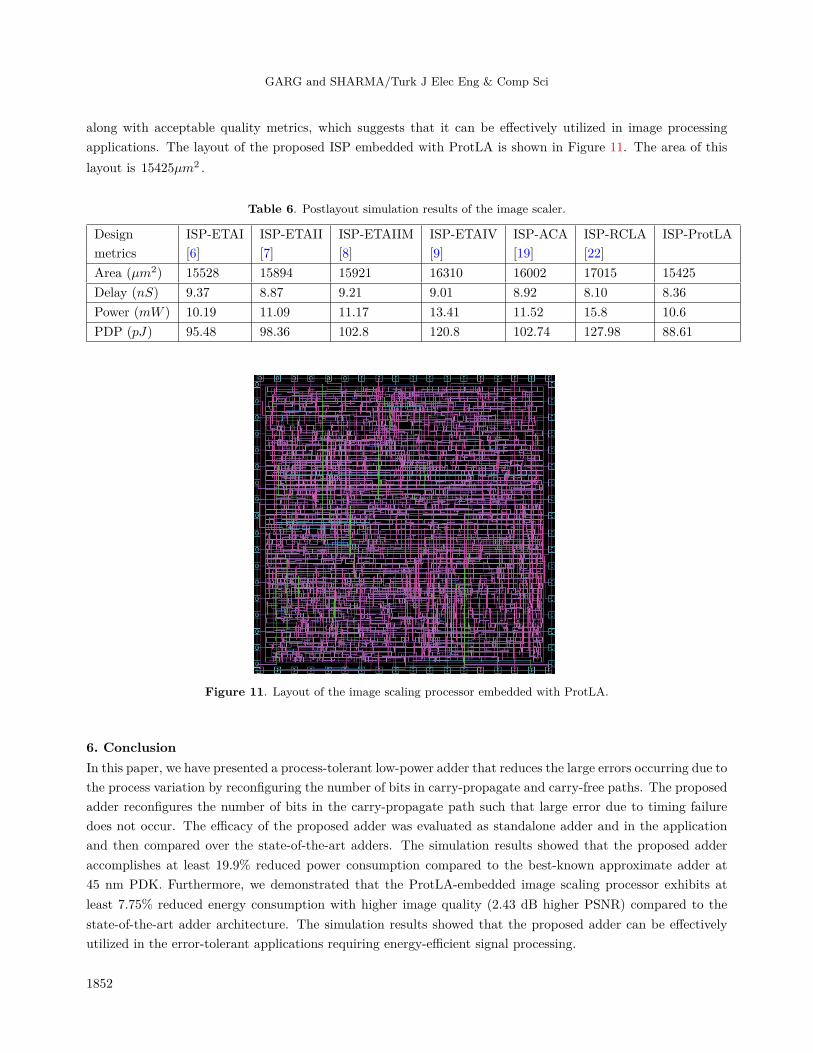
along with acceptable quality metrics, which suggests that it can be effectively utilized in image processingapplications. The layout of the proposed ISP embedded with ProtLA is shown in Figure 11. The area of thislayout is 15425µm2 .
Table 6. Postlayout simulation results of the image scaler.
Design ISP-ETAI ISP-ETAII ISP-ETAIIM ISP-ETAIV ISP-ACA ISP-RCLA ISP-ProtLAmetrics [6] [7] [8] [9] [19] [22]Area (µm2) 15528 15894 15921 16310 16002 17015 15425Delay (nS) 9.37 8.87 9.21 9.01 8.92 8.10 8.36Power (mW ) 10.19 11.09 11.17 13.41 11.52 15.8 10.6PDP (pJ) 95.48 98.36 102.8 120.8 102.74 127.98 88.61
Figure 11. Layout of the image scaling processor embedded with ProtLA.
6. ConclusionIn this paper, we have presented a process-tolerant low-power adder that reduces the large errors occurring due tothe process variation by reconfiguring the number of bits in carry-propagate and carry-free paths. The proposedadder reconfigures the number of bits in the carry-propagate path such that large error due to timing failuredoes not occur. The efficacy of the proposed adder was evaluated as standalone adder and in the applicationand then compared over the state-of-the-art adders. The simulation results showed that the proposed adderaccomplishes at least 19.9% reduced power consumption compared to the best-known approximate adder at45 nm PDK. Furthermore, we demonstrated that the ProtLA-embedded image scaling processor exhibits atleast 7.75% reduced energy consumption with higher image quality (2.43 dB higher PSNR) compared to thestate-of-the-art adder architecture. The simulation results showed that the proposed adder can be effectivelyutilized in the error-tolerant applications requiring energy-efficient signal processing.
1852

GARG and SHARMA/Turk J Elec Eng & Comp Sci
References
[1] Borkar S, Karnik T, Narendra S, Tschanz J, Keshavarzi A, De V. Parameter variations and impact on circuits andmicroarchitecture. In: ACM 2003 Proceedings of the 40th annual Design Automation Conference, 2-6 June 2003,Anaheim, CA, USA: pp. 338-342.
[2] Unsal O, Tschanz J, Bowman K, De V, Vera X, Gonzalez A, Ergin O. Impact of parameter variations on circuitsand microarchitecture. IEEE MICRO 2006; 26: 30-39.
[3] Snigdha FS, Sengupta D, Hu J, Sapatnekar SS. Optimal design of JPEG hardware under the approximate computingparadigm. In: ACM/EDAC/IEEE Proceedings of the 53rd Annual Design Automation Conference, 5-9 June 2016;Austin, TX, USA: IEEE pp. 1-6.
[4] Shafique M, Hafiz R, Rehman S, El-Harouni W, Henkel J. Cross-layer approximate computing: from logic toarchitectures. In: ACM/EDAC/IEEE Proceedings of the 53rd Annual Design Automation Conference, 5-9 June2016; Austin, TX, USA: IEEE pp. 1-6.
[5] Han J, Orshansky M. Approximate computing: an emerging paradigm for energy-efficient design. In: IEEE 2013European Test Symposium (ETS), 27-30 May 2013; Avignon, France: IEEE pp. 1-6.
[6] Zhu N, Goh WL, Zhang W, Yeo KS, Kong ZH. Design of low-power high-speed truncation-error-tolerant adder andits application in digital signal processing. IEEE T VLSI Syst 2010; 18: 1225-1229.
[7] Zhu N, Goh WL, Yeo KS. An enhanced low-power high-speed adder for error-tolerant application. In: IEEE 200912th Proceedings of the International Symposium on Integrated Circuits, (ISIC), 14-16 Dec. 2009; Singapore: IEEEpp. 69-72.
[8] Zhu N, Goh WL, Yeo KS. Ultra low-power high-speed flexible probabilistic adder for error-tolerant applications.In: IEEE 2011 International SoC Design Conference (ISOCC), 22-23 Nov. 2011; Seoul, South Korea: IEEE pp.393-396.
[9] Zhu N, Goh WL, Wang G, Yeo KS. Enhanced low-power high-speed adder for error-tolerant application. In: IEEE2010 International SoC Design Conference (ISOCC), 22-23 Vov. 2010; Seoul, South Korea: IEEE pp. 323-327.
[10] Shin D, Gupta SK. A re-design technique for datapath modules in error tolerant applications. In: IEEE 2008 17thAsian Test Symposium (ATS), 24-27 Nov 2008; Sapporo, Japan: IEEE pp. 431-437.
[11] Gupta V, Mohapatra D, Raghunathan A, Roy K. Low-power digital signal processing using approximate adders.IEEE T Computer-Aided Design of Integrated Circuits and Systems 2013; 32: 124-137.
[12] Du L, Varman P, Mohanram K. High performance reliable variable latency carry select addition. In: IEEE 2012Design, Automation & Test in Europe Conference & Exhibition (DATE), 12-16 March 2012; Dresden, Germany:IEEE pp. 1257-1262.
[13] Mazahir S, Hasan O, Hafiz R, Shafique M, Henkel J. An area-efficient consolidated configurable error correctionfor approximate hardware accelerators. In: ACM/EDAC/IEEE 2016 Proceedings of the 53rd Annual DesignAutomation Conference, 5-9 June 2016; Austin, TX, USA: IEEE p. 96.
[14] Pashaeifar M, Kamal M, Kusha AA, Pedram M. Approximate reverse carry propagate adder for energy-efficientDSP applications. IEEE VLSI Syst 2018; 99: 1-12.
[15] Huang J, Lach J, Robins G. A methodology for energy-quality tradeoff using imprecise hardware. In: IEEE 2012Proceedings of the 49th Annual Design Automation Conference, 3-7 June 2012; San Francisco, CA, USA: IEEE pp.504-509.
[16] Ayhan T, Kula F, Altun M. A power efficient system design methodology employing approximate arithmetic units.In: IEEE 2017 Computer Society Annual Symposium on VLSI (ISVLSI) 3-5 July 2017; Bochum, Germany: IEEEpp. 243-248.
[17] Lee S, John LK, Gerstlauer A. High-level synthesis of approximate hardware under joint precision and voltagescaling. In: IEEE 2017 Proceedings of the Conference on Design, Automation & Test in Europe (DATE), 27-31March 2017; Lausanne, Switzerland: IEEE pp. 187-192.
1853

GARG and SHARMA/Turk J Elec Eng & Comp Sci
[18] Rahimi A, Benini L, Gupta RK. Accuracy-configurable OpenMP. From Variability Tolerance to ApproximateComputing in Parallel Integrated Architectures and Accelerators, Springer 2017, 133-149.
[19] Kahng AB, Kang S. Accuracy-configurable adder for approximate arithmetic designs. In: IEEE 2012 49thACM/EDAC/IEEE Design Automation Conference (DAC), 3-7 June 2012; San Francisco, CA, USA: IEEE pp.820-825.
[20] Shafique M, Ahmad W, Hafiz R, Henkel J. A low latency generic accuracy configurable adder. In: 52ndACM/EDAC/IEEE Design Automation Conference (DAC), 8-12 June 2015; San Francisco, CA, USA: IEEE pp.1-6.
[21] Garg B, Dutt S, Sharma GK. Bit-width-aware constant-delay run-time accuracy programmable adder for error-resilient applications. Microelectronics Journal 2016; 50: 1-7.
[22] Akbari O, Kamal M, Kusha AA, Pedram M. RAP-CLA: A reconfigurable approximate carry look-ahead adder.IEEE T Circuits and Systems II: Express Briefs 2018; 65: 1089-1093.
[23] Banerjee N, Karakonstantis G, Roy K. Process variation tolerant low power DCT architecture. In: IEEE 2007Proceedings of the conference on Design, automation and test in Europe, 16-20 April 2007; Nice, France: IEEE pp.630-635.
[24] Karakonstantis G, Banerjee N, Roy K. Process-variation resilient and voltage-scalable DCT architecture for robustlow-power computing. IEEE T VLSI Syst 2010; 18: 1461-1470.
[25] Garg B, Chaitanya GVNSK, Sharma GK. A low-cost energy efficient image scaling processor for multimediaapplications. In: IEEE 2016 Symposium on VLSI Design and Test (VDAT), 24-27 May 2016; Guwahati, India:IEEE pp. 1-6.
[26] Liang J, Han J, Lombardi F. New metrics for the reliability of approximate and probabilistic adders. IEEE TComputers 2013; 62: 1760-1771.
[27] Wang Z, Bovik AC, Sheikh HR, Simoncelli EP. Image quality assessment: from error visibility to structuralsimilarity. IEEE T Image Processing 2004; 13, pp. 600-612.
1854