a performance study of the acorn risc machine
TRANSCRIPT
A Performance Study
of the Acorn RISC Machine
A thesis
submitted in partial fulfilment
of the requirements for the Degree
of
Master of Science in Computer Science
in the
University of Canterbury
by
David Vivian Jaggar
University of Canterbury
1990
Abstract
The design decisions behind the development of the Acorn RISC Machine
(ARM) are investigated, by implementing the architecture with a software
emulator, to record the effectiveness of the unusual architectural features
that make the ARM architecture unique.
The adaption of an existing compiler construction tool (the Amsterdam
Compiler Kit) has demonstrated that an optimising compiler can exploit
the RISC architecture to maximize CPU performance.
By compiling high level language algorithms, a complete picture of the
effectiveness of the ARM architecture to support high performance
computing is formed.
-2-

Contents
Abstract ....................................................................................... 2
Contents ....................................................................................... 3
Figures and Tables ........................................................................ 5
Computer Design .......................................................................... 7
The Central Processing Unit ................................................... 7
The Instruction Set ................................................................ 8
Microcode ............................................................................ 12
Registers ............................................................................. 13
The Memory ........................................................................ 14
Advancing Technology ......................................................... 21
RISC Architectures ..................................................................... 24
Improving Performance ....................................................... 26
Cycles per Instruction .......................................................... 26
Time per Cycle ..................................................................... 29
Instructions per Task ........................................................... 30
RISC Development ............................................................... 32
Commercial RISC Designs ................................................... 35
Other Commercial RISC Architectures .................................. 43
The Acorn RISC Machine ............................................................ 45
Architecture Characteristics ................................................. 48
The Impact on Performance .................................................. 00
Evaluating an architecture .................................................... 63
Computer Software ..................................................................... 64:
The Operating System .......................................................... 64:
Compilers ........................................................................... 65
Application Programs .......................................................... 74
An Optimising Compiler for ARM ................................................ 76
-3-

Compiler Building Tools ....................................................... 76
EM code and the Code Generator Generator ............................ 00
Global and Peephole Optimisers ............................................ 89
The Assembler and Linker .................................................... 89
The After-Burner Optimiser ................................................. 00
Register Allocation ............................................................... 92
Compiler Validation ............................................................. 95
Evaluating an Architecture .......................................................... 96
Architectural Features ......................................................... 96
Measuring the Quality of an Architecture ............................... 00
Architectural Emulation ..................................................... 100
Emulator Validation and Performance .................................. 103
The Quality of the ARM Architecture ........................................... 105
Compiler Performance ........................................................ 106
Architecture Performance ................................................... 109
Instruction Usage ............................................................... 110
Branch and Conditional Instruction Utilisation ...................... 115
Memory Accessing Instructions ........................................... 118
Cache Effectiveness ............................................................. 119
Improving the ARM architecture ......................................... 120
Conclusion ................................................................................ 127
Acknowledgements .................................................................... 130
Bibliography .............................................................................. 131
ARM 3 Instruction Set Format .................................................... 136
EM Instruction Set ..................................................................... 139
Floating Point Accelerator Instruction Set .................................... 145
-4-

Figures and Tables
Figure 1: A Simple CPU ...................................................................... 8
Figure 2: An Instruction Pipeline ...................................................... 'Z7
Figure 3: SPARC Register Window Layout .......................................... 38
Figure 4: ARM Register Layout ......................................................... 52
Figure 5: ARM Shift Operations ......................................................... 53
Figure 6: Compiler Stages ................................................................. fJ7
Figure 7: ARM Signed Divide Routine ................................................ f57
Figure 8: Emulator Execution Breakdown .......................................... 104
Figure 9: Acorn and ACK Compiler Performance ............................... 107
Figure 10: Relative Instruction Usage ............................................... 111
Figure 11: Data Processing Instructions ............................................ 113
Figure 12: Data Processing Operands ................................................ 114
Figure 13: Data Processing Immediate Operands ............................... 116
Figure 14: Conditional Non-Branch Instructions ............................... 117
Figure 15: Addressing Modes ........................................................... 119
Figure 16: Cache Strategies .............................................................. 12A
Table 1: A Simple Instruction Set ....................................................... 10
Table 2: Code Size for CISC (MC68020) and RISC (SPARC) .................... 31
Table 3: Relative Frequency of High Level Language Statements ............ 36
Table 4: ARM Instruction Set ............................................................ 46
Table 5: Architectural Benchmarks .................................................. 105
-5-

To my Mother and Father
-6-

Chapter 1 Computer Design
The performance of a computer system is measured by the time that it
takes to execute programs, the shorter the elapsed time the higher the
performance rating. To maximise the performance a designer must find
ways to match the performance of each component in the computer, to
yield a balanced system. As technology changes and new discoveries are
made, different parts of a computer become the performance bottle-neck.
The architecture of a computer defines the major attributes of the design.
The number of registers, their layout, the instructions and addressing
modes that the computer understands are all part of the architecture,
while the number of clock cycles taken to execute each instruction, the
type of transistor logic used to build the CPU, and the layout of memory
are part of the implementation.
The Central Processing Unit
The Central Processing Unit (CPU), as shown in Figure 1, is the part of
the computer that executes instructions. The CPU is composed of a
number of specialized functional units (for example the Arithmetic Logic
Unit, or ALU). These functional units are controlled by the Instruction
Decoder, which activates the necessary sections of each unit to carry out
the operation specified by each instruction. Each functional unit is
connected by data paths, along which data, parts of decoded instructions
and internal control information flows.
-7-

A Bus BBus
Figure 1: A Simple CPU
The Instruction Set
The instruction set of a computer (the machine code) is the language that
is used to directly program the CPU. The instruction sets of computers are
significant factors in the overall price/performance of the machine. Each
instruction of the CPU must be implemented using digital logic that must
be custom designed (using "microprogramming" to replace some logic by
sacrificing performance is discussed later). This "custom silicon" is
extremely labour intensive to construct, so that a large and/or complex
instruction set is very expensive to implement in hardware. Emulating
some instructions with software is less expensive, but lowers the
performance of the computer, due to the inefficiency of using
combinations of the existing instructions to emulate missing instructions.
Whilst machines exist whose instruction set is tailored for one specific
high level language, such a design would be inappropriate for a general
-8-

purpose microcomputer. Table 1 illustrates a simple instruction set. An
instruction set must be able to efficiently support the many unique
features specific to different high level languages, although programming
languages have major features in common -
i) arithmetic operations for integer and floating point data.
An instruction set will need operations to move data to and from the
memory and registers, and be able to perform some simple
arithmetic on that data. Integer addition and subtraction
instructions are found in the simplest of CPUs, while multiply and
divide are quite common in more complex architectures. The results
of such instructions usually update the processor's condition flags: a
negative result will set the negative flag, a zero result will set the zero
flag, a carry or borrow from additions and subtractions will set the
carry flag, and an overflow will set an overflow flag. Floating Point
operations are usually carried out in a totally separate processor, the
Floating Point Unit (FPU), but the functions it performs are similar
to the integer unit.
ii) operations on Boolean data.
Boolean values, arrays of Boolean values, and sets require bit-wise
logical operators like And, Or and Exclusive Or. The And operator is
used to clear a bit, Or is used to set a bit, and Exclusive Or is used to
toggle a bit. Operations on bit fields such as Not, Left Shift, Right
Shift and Rotate can be used to build values for comparison with
Boolean data.
-9-
Instruction Mnemonic
Add ADD
Subtract SUB
Logical AND AND
Logical OR OR
Logical EOR EOR
Logical NOT NOT
Logical Shift Left LSL
Logical Shift Right LSR
Rotate ROT
Arithmetic Shift Right ASR
Compare CMP
Move MOV
Multiply MULT
Divide DIV
Jump JMP
Procedure Call CALL
Procedure Return RET
Conditional Branch Bee
Where : Dest , Srcl and Src2 are registers or memory addresses
PC is the program counter
cc is a condition code
offset is an address offset
Table 1: A Simple Instruction Set
Operation
Dest := Srcl + Scr2
Dest := Srcl- Src2
Dest := Srcl AND Src2
Dest := Srcl OR Src2
Dest := Srcl EOR Src2
Dest := NOT Srcl
Dest := Srcl * 2Src2
Dest := abs(Srcl I 2Src2)
Dest := Src 1 Rotated Src2 bits
Dest := Srcl I 2
Srcl- Src2
Dest := Srcl
Dest := Srcl * Src2
Dest := Srcl I Src2
PC:= Dest
Dest := PC, PC := Dest
PC:= Dest
IF cc PC:=PC+offset
iii) support for the conditional execution of instructions depending on
some previous condition.
A compare instruction can be used to compare two pieces of data. The
condition flags are usually set to reflect the result of the last compare
instruction, the negative flag indicating which operand was the
larger and zero flag if they were equal. A branch instruction will
jump to a different part of the program depending on the state of one
- 10-

or more condition flags, for example "Branch on Greater Than or
Equal to". Many architectures combine the compare and branch
instructions, as they are usually used together. These instruction are
used to implement IF statements, conditional loops (FOR, WHILE etc.)
and CASE type statements.
iv) jump instructions to change the flow of execution.
High level language constructs like infinite loops, premature loop
terminators and GOTO statements require a Jump instruction to
unconditionally alter the value held in the program counter.
v) constructs to implement procedure calls.
By storing the current value of the program counter, and using a
jump instruction, a program can execute a procedure and then
continue execution just after the point of call by jumping back to the
value in the stored program counter. If the return address is pushed
onto a stack, then procedure calls can be nested, and procedure
recursion is possible.
vi) addressing modes to access data structures held in memory.
Data structures like Pascal's arrays and records require the
processor to be able to load data to and from an address determined by
adding an offset to a base address. The base address holds the
address of the start of the array or record and the offset holds the
distance of the required element from the beginning. These same
addressing modes can be used to access data held in the stack frame
of a procedure held on the stack.
- 11-
Of course, all programming languages have their own characteristic
features, and a general purpose architecture must cater for these. The
microprocessors designed in the early 1980's added many instructions
and addressing modes to the simple instruction set shown in Table 1 to
add hardware support for the features of many high level languages. This
has the unfortunate side effect that some instructions will be completely
useless in some situations, effectively a waste of "silicon real estate" on the
CPU chip.
Microcode
The amount of custom logic required to directly implement a very large
instruction set to support high level languages is too large to fit on a single
chip. Only implementing a small number of instructions in hardware
and emulating all others in software is inefficient, due to the overheads
involved in the trap handler for unimplemented instructions (each
unimplemented instruction must be fetched from memory, decoded in
software, and its action emulated with other instructions). Microcode is a
very low level instruction format that is suitable for complete
implementation in hardware, and is tailored for the efficient emulation of
machine code instructions. Each machine code instruction is executed by
running a sequence of microcode instructions (called a micro program).
The microcode sequences are stored in a Read Only Memory (ROM) that is
part of the CPU. The uniform nature of a ROM makes much more
efficient use of logic than the custom logic used in a functional unit, so
that the entire machine code instruction set can be implemented.
Microcode is extremely tedious to write, because the program must obey
stringent timing restrictions when accessing each functional unit of the
CPU. Thus the microcode is usually fixed at the time of manufacture, and
- 12-

the CPU can be programmed using the higher level machine code.
Different implementations of the same architectures can be produced by
adding extra functional units to the CPU to eliminate the need for certain
microcode sequences. Microcoding is a price/performance compromise -
another level of interpretation has been added to the CPU which, although
it reduces the cost and makes more efficient use of chip space, also lowers
the performance compared to a CPU with a complex "hard-wired"
instruction set.
Registers
The program data is usually kept in registers in the CPU while it is being
referenced frequently, so that access to it is as fast as possible. The ALU
and registers are connected by data paths, called buses, which carry 32
bits of information in parallel in a 32 bit computer. The buses connect to
the register file via a port. The register file will need two read ports and a
write port if an instruction like "add the contents of two registers and store
the result in a third register" is to be executed in a single clock cycle. The
registers are arranged in a bank (or file), which usually consists of a
small, fast Static Random Access Memory (SRAM). The actual number of
registers is usually limited by the number of bits required in each
instruction word to encode the register numbers and the amount of CPU
chip area that is available. Not all CPU's have registers (data is accessed
directly in memory [Ditz87]), some have as many as 192 [AMD87, Lehr89],
but typical numbers are 16 and 32.
- 13-
The Memory
The memory of the computer stores instructions and data. Several
separate memory chips are attached to one memory controller to provide a
homogeneous memory bank. The CPU is connected to a memory
controller via two buses, the data bus (which carries data to and from the
memory) and the address bus (which dictates the required memory
address). The memory controller is responsible for activating the correct
memory chip(s) for the memory address required.
Size and speed of memory are major influences on the cost and the
execution speed of the computer. The size of the memory is directly
proportional to the cost; pay twice as much and get twice as much.
Modern microcomputer applications need at least 1 MegaByte of main
memory, larger machines have 8 to 16 MegaBytes. The speed of the
memory is more subtly related to the cost, being dependent on two factors-
(i) Latency.
The time taken for the memory to return the first word of data.
(ii) Bandwidth.
The rate at which data can be transferred to the CPU, once the initial
flow is established.
The execution speed of a program is dependent on both these factors. The
performance of a program that consists entirely of jump or branch
instructions and data accesses to non contiguous memory locations will be
limited by the memory latency, because after every branch or jump the
memory must restart the flow from a new location, while the performance
of a program that has no branch or jump instructions and contiguous
- 14-

data accesses will be limited by the memory bandwidth. Of course a real
program will have some branch or jump instructions and some random
and some contiguous data memory accesses, so the demand on the
memory will be between these two extremes. There are several ways of
increasing memory access speed -
(i) Faster Memory Devices.
Using faster memory chips will increase the bandwidth and reduce
the latency. Dynamic Random Access Memory (DRAM) can deliver
up to about 6 Million random accesses per second. To gain more
speed than this, Static Random Access Memory (SRAM), which can
provide 100 Million accesses per second, must be used. The price
difference between DRAM and SRAM makes it too expensive to build
a microcomputer with a memory made only of SRAM; a compromise
is discussed below, which utilises both SRAM (for speed) and DRAM
(for its low cost) to implement a fast, relatively inexpensive memory.
(ii) Wider buses.
Multiple memory devices connected in parallel, each connected to the
same memory controller, increases the memory bandwidth but does
not alter the latency. A bus that is twice as wide will deliver nearly
twice the usable performance despite the wastage that occurs due to
operations involving data objects much smaller than the bus size (for
example, byte operations on a 16 bit bus leaves the bus 50% unused,
whilst on a 32 bit bus the bus is 75% unused). Unfortunately
increasing the size of a memory bus beyond 32 bits is currently too
expensive to be used in a low cost micro-computer.
- 15-
(iii) Interleaved memory banks.
Multiple (interleaved) memory devices connected in parallel to
separate memory controllers allow one bank of memory to supply
data to the processor while the other(s) are recovering from
supplying previous data. This increases both the bandwidth (because
separate banks have more time to recover between accesses) and
reduces the latency (because on average a memory access will be to a
memory bank that has already had some recovery time), but the
added cost of a separate memory controller for each bank of memory
may be prohibitive.
(iv) Fast access modes.
By exploiting the physical layout of DRAM consecutive memory
accesses to sequential memory locations can be significantly faster
than completely random ones, without increasing the price of each
memory device. These type of DRAMs are known as Page Mode
DRAMs or Static Column DRAMs. This technique will increase the
bandwidth of the memory, but not alter latency. The cost of this
implementation is merely adding an extra control line from the CPU
to the memory system to indicate that the current memory reference
is in sequence with the last.
v) Harvard architecture.
Rather than storing both instruction and data in a single memory (a
von Neumann architecture), there may be two physically separate
memories for instructions and data- a Harvard architecture, to
double the memory bandwidth. Of course a Harvard architecture will
require two address buses and two data buses, but it will be possible to
read the next instruction and perform a load or store operation in
- 16-

parallel. This extra performance comes with the cost of building a
computer with twice as many bus lines, which is extremely
expensive.
vi) Cache memory.
Because programs tend to reference the same areas of memory
repeatedly (while executing loops and accessing data structures in
memory) it will be more efficient to store frequently used instructions
and data temporarily in a small, very fast SRAM, rather like holding
data in CPU registers while it is being accessed, and use less
expensive DRAM for the rest of the memory. Every time data is
loaded from DRAM it is stored in the SRAM "cache" as well as being
passed to the CPU. Then if the CPU requests this same data from the
memory again, it can be supplied much sooner from the cache,
allowing the CPU to maintain its maximum instruction and data
throughput.
A cache "hit" occurs when the requested data currently resides in the
cache, a cache "miss" occurs when requested data does not reside
there. The performance of a cache is measured by its hit ratio - the
proportion of cache hits in relation to the total number of memory
references. The hit ratio of a cache is dependent on various design
parameters, for instance the algorithm used to decide where to put
new data in the cache. The following algorithms are suitable for a
fast implementation in hardware-
a) Direct Mapped Cache.
This is the simplest system: low order bits of the main memory
address are used to determine a unique location in the cache
- 17-

memory for the data. Unfortunately if a program references two
blocks of memory that have the same low order address bits, the
cache will be repeatedly filled with new data (or instructions)
from alternate memory blocks, continually overwriting data that
will be required again.
b) Dual Set Associative Cache.
To ease the problem with a direct mapped cache, two locations
can be reserved for each low order address bit combination, and
new data will be placed in the Least Recently Used (LRU) location.
A single bit is enough to record the last location used. Now three
separate memory references with the same low order address bits
will be required to spoil the cache's efficiency; this situation is
very rare.
c) Multi Set Associative Cache.
The associativity of the cache may be increased to four or further,
but the LRU algorithm for deciding the position of new data
becomes much more complex. The associativity is usually a
power of two because this makes the most efficient use of LRU
hardware.
d) Fully Associative Cache.
Now each item of data can reside anywhere in the cache, and
corresponding addresses must be stored to identify the data. A
content addressable memory is used to store the data. This special
memory instantaneously returns the data associated with an
identifier (in this case the data associated with a memory
address). A disadvantage of this scheme is the need for every
- 18-

piece of data in the cache to have its associated address stored
with it, using up valuable hardware space that could have been
used to make a larger, less complex cache. The solution is to store
the contents of a number of successive locations with a single
address, called a cache line. When a cache miss occurs, a
complete cache line is fetched from the main memory. Although
this sounds theoretically inefficient, in practice sequential cache
locations are likely to be accessed together anyway, thus caching
an entire line at once allows for the utilisation of the page mode
access feature of the DRAM main memory. Using an LRU
algorithm to find a location for new data in a fully associative
cache is very complex to implement in hardware, and has a
pathologically worst case when the number of items to be cached
is just bigger than the size of the cache and the items are always
accessed in the same order (such as the instructions in a loop or
the elements of an array)- the LRU algorithm always replaces
oldest (soon to be needed) data in the cache with the new data, so
the cache always misses. An alternate to LRU is a random
replacement scheme. The value from a fast counter is used to
provide a pseudo random location for new data. This scheme is
easy to implement, and works as well as LRU whilst avoiding
LRU's pathological case.
The cache can be used for virtual or physical memories (or even
separate caches for each), and each alternative has disadvantages. A
virtual memory (or "virtually mapped") cache will need to have some
entries invalidated every time a new page translation is calculated,
and a physical memory (or "physically mapped") cache will be slowed
because it must wait for the virtual to physical address translation
- 19-
before it can look up any data. Both these types of cache are common
in commercial computers.
There are two ways of maintaining the consistency of data between
the cache and the main memory when a memory store operation is
executed-
a) Write through.
The obvious approach is to write data to the cache and main
memory at the same time. Unfortunately this simple scheme
means that main memory will be referenced by every store
operation, which is contrary to the caching principle.
b) Write back.
Data can be just written to the cache and then copied to memory if
the cache entry is ever to be overwritten again. This strategy will
avoid memory references between successive writes to the same
memory address, but requires a "dirty" flag for each cache entry
to indicate if the data needs to be saved back to memory before the
location is reused.
A "write buffer" can be used in with either strategy to allow the
processor to continue instead of waiting for the data to be written to
main memory.
A cache memory is particularly useful for a Harvard architecture.
Instead of having two separate main memories for instructions and
data, two caches are used, one for instructions, the other for data.
Separate address and data buses are still required for instructions
-20-

and data, but they only connect to their associated caches, because
both caches share a common address and data bus to access a
common main memory. The main memory only needs enough
bandwidth to supply data for cache misses, rather than all CPU
traffic. For a more complete description of cache principles see
[Smit82]
It is possible to combine two or more of these implementation techniques
to achieve the performance required for a microcomputer memory
system.
Advancing Technology
The microprocessors designed in the early 1980's tended to have large
number of complex instructions and addressing modes, intended to
provide similar computational power with a single chip CPU as the
mainframe computers of the 1970's achieved with their multiple chip (and
usually multiple circuit board) CPU s. This level of micro-processor
complexity was made possible by the advent of Very Large Scale
Integration (VLSI), and the resulting computers using these micro
processors have become known as Complex Instruction Set Computers
(CISCs). This complexity was used to alleviate several problems-
i) Slow core memory.
The magnetic core memory used for main memory was very slow
compared to the speed of access to the on-chip microcode ROM,
causing the execution time of programs to be proportional to the
number of instructions in the program. Thus more complex
-21-

instructions were implemented with microcode to replace sequences
of simple instructions, to avoid repeated accesses to core memory.
ii) Compact assembly language.
Complex instructions aided assembly language programmers by
replacing common sequences of instructions with a single
instruction. As software was becoming a significant factor in the cost
of a computer system, and a large proportion of software was written
in assembly code to reap the maximum performance of the machine,
any such aid given to assembly language programmers would be
useful.
iii) High level language support.
Complex instructions and addressing modes were thought to help
compiler builders by closing the semantic gap between high level
languages and assembly language. Designers supported high level
language features with fast hardware to improve performance.
Making high level languages efficient was also important to help
keep software costs down.
iv) Good compiler targets.
These complex designs had few registers, because compilers for
stack or memory to memory architectures were far easier to
construct. Registers were difficult to allocate optimally for local
variable use, so were mainly used as temporary storage in
expression evaluation, and as pointers to data structures.
v) Easily adaptable.
Microcode was an efficient way to utilise the advancing technology
-22-
used to build a CPU. As more transistors could be placed on a chip,
more microcode could easily be added to build a bigger and more
complex instruction set, and more dedicated hardware could be
added to speed up microcode instructions.
The Digital Equipment VAX architecture is a good example of an
elaborate instruction set, with instructions for polynomial evaluation,
queue manipulation and cyclic redundancy checks. The Intel 80x86 series
microprocessors are some of the most complex, having instructions to
operate on entire strings, complex looping instructions and table look up
instructions. The Motorola 680x0 series has instructions to insert and
extract bit fields to and from a word, to search words for a set or clear bit,
and complex module calling instructions.
-23-

Chapter2 RISC Architectures
There are several deficiencies with the Complex Instruction Set approach
to improving computer performance-
i) Compilers cannot utilise the complexity.
Modern compilers have extreme difficulty applying complex
instructions to high level languages. Complex instructions rarely
perform the exact task required by a high level language: if an
instruction does not quite do what is required then its action must be
modified with other instructions, or completely replaced with new
instructions. An instruction that does more than is required is
wasting execution time doing wasted work. In tracing compiled code
executing on a complex architecture, researchers noticed that the
same twenty percent of instructions accounted for eighty percent of
all executed instructions, and a further ten percent of instructions
accounted for almost all instructions executed. The remainder of the
instruction set was unused and therefore unnecessary. [Sun87a].
ii) Complexity implies poor performance.
Complex instructions take a long time to load from core memory and
take a long time to decode. Because of the variable lengths of complex
instructions, each must be partially decoded before it can be executed.
This complexity makes it extremely difficult to have a complex
instruction loaded and decoded, ready for execution after a sequence
of fast instructions, so the ALU must wait for the complex
instruction to be loaded and decoded. Even worse, the complex
instructions add extra length to the main execution data path which
-24-
decreases the execution speed of all instructions. Thus an instruction
which lengthens a data path by ten percent must increase the
execution speed of programs by more than ten percent to be justified.
iii) Memory to memory architectures are inefficient.
Although it is difficult to write compilers for register based
architectures, registers are very efficient for the storage of variables
and procedure parameter values. Memory to memory models access
memory too often to be as efficient. Stack based machines can be
made efficient, but a considerable amount of hardware is still
required to approach the efficiency of registers.
iv) Assembly language is a slow programming environment.
The compiler that can produce good machine code from a high level
language will replace the assembly language programmer, because
writing programs in assembly language is too slow to use for most
programming tasks. A good architecture should make it possible for
a good optimising compiler to produce code of comparable quality to
assembly language programmers.
v) Long design time.
Complex architectures are difficult to design, take a long time to
verify and manufacture, and therefore cannot be designed to take
advantage of the latest technological advances.
-25-

hnproving Performance
The time it takes for a computer to perform a task is a product of three
factors-
Time per Task = C x T x I
where C is the cycles per instruction
T is the time per cycle
I is the instructions per task
Improving any of these factors will improve performance. The first two
factors tend to be complementary - an architecture may have a long cycle
time to accommodate complex instructions, or it may have multiple
(shorter) cycles per instruction.
Complex Instruction Set Computers attempt to minimise the time per
task by minimising the instructions per task, by making each instruction
do a lot of work. In practice this lengthens either or both of the cycles per
instruction and the time per cycle in greater proportion, so that
performance suffers as a result.
Reduced Instruction Set Computers (RISCs) follow new computer
architecture and implementation design disciplines -minimising the
number of cycles per instruction and decreasing the cycle time to increase
performance.
Cycles per Instruction
RISCs achieve a short cycle time by implementing a very simple, but very
fast instruction set. This simple instruction set allows several
instructions to be "pipelined" - several instructions are at different stages
-26-

of execution at one time, to maximise the usage of different functional
units of the processor. Figure 2 shows a pipeline with five stages,
instruction load, decode, register read, ALU operation, register write.
Instructions still require several cycles to be executed, but because each
stage is done in parallel with other instructions at a different stage, a
throughput approaching one instruction per cycle can be maintained.
Instruction 1
Instruction 2
Instruction 3
• • • Time
Figure 2: An Instruction Pipeline
Data dependencies occur between each instruction in the pipeline because
an instruction can read from the registers before the previous instruction
has written its results. These dependencies are resolved by adding
forwarding logic to the CPU to by-pass the register file, routing the result
value directly from one instruction to the input value of the next
instruction.
The number of cycles each instruction adds to the total number of cycles
taken to execute a program is potentially reduced by the number of stages
in the pipeline (called the pipeline depth). Fulfilling this potential requires
the pipeline be always filled with instructions, a task that is very difficult
unless all instructions are the same (encoded) length, and take
approximately the same amount of time to execute. So RISC instructions
-27-
are always one (usually thirty two bit) word long, and most require only a
single cycle AL U operation. A CISC architecture cannot fully achieve
either of these goals: its complex instructions are impossible to encode
using the same number of bits or to execute in the same time period (cycle
length). The data paths in a RISC architecture need only carry word sized
objects around the CPU, a CISC architecture must be able to move its
multi word instructions around the CPU, which adds cost and
complexity.
Instructions that change the value of the program counter (branches,
jumps, traps, procedure calls and procedure returns) make it difficult to
keep the instruction pipeline full. To avoid stalling the CPU while new
instructions are loaded from the new memory location, instructions like
branch are usually implemented with a delayed action: the instruction
immediately after the branch instruction (said to be in the branch delay
slot) is always executed after the branch instruction is executed. The
compiler can often find an instruction to put in the delay slot to do useful
work, if it cannot a NOP (No-OPeration) instruction must be inserted.
Instructions that access memory require special attention for two
reasons. Firstly a full memory addressing mode takes many instruction
bits to encode - too many to specify each operand of every thirty-two bit
instruction, so a "load/store" architecture is implemented: only the load
and store instructions can access memory; all other instruction only
access data that is held in registers. The second problem is that the data
from a load instruction will not be available to all subsequent instructions,
due to the slow access speed of main memory. The solution is to provide
delayed load instructions, the instruction after the load (in the load delay
slot) cannot access the register into which the load instruction will place
-28-

the data. Again the compiler attempts to find a suitable instruction for the
load delay slot, if this is not possible a NOP must be inserted.
Time per Cycle
The length of a single machine cycle is determined by several factors.
Firstly the instruction decode time is related to both the number of
instructions in the instruction set and the number of instruction formats
supported. Clearly a CISC architecture will require a longer decode time
than a RISC architecture. Most RISC architectures have only a few levels
in their decode strategy: the instructions are first split into broad
"families" by examining a few key bits in each word, then each instruction
can be fully decoded. Complex addressing modes in CISC architectures
lengthen the decode time substantially, although the National 32x00 series
of processors have a very uniform instruction set, which results in a fast
instruction decode time. Other CISC architectures, such as the Motorola
680x0 and Intel 80x86 architectures have very complex instruction
formats, due to their backward compatibility with their respective
ancestors.
The second factor in the time per cycle is the instruction operation time.
RISC architecture instructions usually have a single cycle ALU stage, so
that the flow of instructions through the processor is not interupted.
Instructions that require more ALU work (such as integer multiply and
divide) are often set running in parallel with single cycle instructions.
CISC architectures have many multi-cycle instructions, which makes
efficient pipelining of instructions very difficult. Considerable amounts of
extra hardware are required to support data dependencies between
instructions (i.e. the result of one may be required for a source operand of
-29-

the next instruction), which uses precious chip space and lengthens
critical processor data paths.
The time needed to fetch instructions from main memory is the third
factor influencing the time per cycle, and is inversely proportional to the
memory bandwidth. Instruction memory latencies are only incurred by
instructions that alter value of the program counter, as new instructions
must be loaded from a new memory address. The techniques described in
Chapter 1 can be utilised to increase the memory bandwidth to decrease
its influence on the time per cycle. RISC architectures can load a new
instruction in every memory access, because all instructions are the same
length. CISC architectures require multiple memory accesses to load
multi word instructions, again making efficient pipeline management
much more complex.
The last factor in the time per cycle is caused by the basic architectural
complexity of an architecture. RISC designers can spend more time hand
optimising critical processor features such as the processor data path and
functional units. CISC architectures have a much longer design and
· implementation cycle, and hand optimising a complex architecture is a
task too large to be practicable.
Instructions per Task
Because of the simple instruction set, RISC architectures require more
instructions than CISC architectures to perform the same task. Table 2
illustrates the length of the machine code of fifteen UNIX utilities, for two
common architectures, a Motorola 68020 [Moto85] based Sun 3/60, and a
SPARC based SUN SPARCstation [Sun87b], using similar compiler
-30-

technology, and compiling for the same Operating System. The 68020
CISC architecture has quite compact machine code, the SP ARC
architecture is a good example of a RISC architecture.
SPARQ Program MC68020 SPARC MC68020
awk 43856 50014 1.14 be 10314 12462 1.21 cmp 3000 3232 1.08 csh 91902 118138 1.29 diff 20752 25512 1.23 eqn 25726 29306 1.14 grep 7174 9394 1.31 Is 8608 10536 1.22 nroff 54826 71162 1.30 od 7232 8560 1.18 sort 12194 15658 1.28 tee 2800 2992 1.07 unpack 4936 6104 1.24 write 5302 6142 1.24 yacc 28909 37730 1.31
Table 2: Code Size for CISC (MC68020) and RISC (SP ARC)
The code expansion is not as great as might be first expected, because the
RISC architecture contains the twenty or thirty percent of instructions
that the compiler could generate for the CISC architecture, which almost
negates the code expansion which might be caused by having only simple
instructions. The expansion that does occur is due to the simple (low
information density) RISC instructions- to speed up the instruction
decode stage. In practice the performance loss caused by the code
expansion is outweighed by the performance gains made by decreasing
the cycle time and reducing the average number of cycles per instruction.
Optimising compilers also help to mitigate the code expansion in RISC
architectures, the simple instruction set means the code sequence for a
-31-
given high level language statement is much easier to generate,
compared to the complex alternatives a CISC may offer. The simple
instructions also offer better opportunities for optimisation, they only
perform the actions required, whereas CISC instructions often have
useless side effects. Simple instructions allow the compiler to re-order
code, to avoid data dependencies and remove code duplication, operations
which are of course impossible with fixed microcode sequences. A simple
architecture also shortens hardware development time, allowing RISC
implementations to utilise the latest hardware technology, and the
resulting implementations are much more likely to operate correctly
(unlike CISC machines which usually undergo several hardware
revisions). The compiler can be continually improved to fully utilise the
hardware.
In practice the effect of such streamlining of an architecture is a large
performance increase, with a lower hardware cost due to the short
development time, resulting in a significant decrease in the
price/performance ratio compared to CISC architectures.
RISC Development
In 1975 IBM began a project to "achieve significantly better
cost/performance for High Level Language programs than that attainable
by existing systems" [Radi82]. The 801 project had pioneering design goals
for a computer architecture, which now form the basis of RISC
architecture and implementation design decisions -
i) maximum utilisation of all sections of the CPU.
A three stage instruction pipeline was designed so that instructions
-32-

could take three cycles to execute: the first cycle was used to load the
instruction from memory, the next cycle to decode the instruction,
read the operands and perform the AL U operation, and the last cycle
to perform shift operations, write the result and set the processor
flags. Functions that needed a longer time to execute, for instance
integer multiplication and division, were handled with a primitive
step instruction. Several multiplication step instructions must be
executed sequentially to perform a complete multiplication. An
effective throughput of one instruction per cycle was realised.
ii) regular instruction format to simplify the decoding of instructions.
All instructions were made one word (four bytes) long and aligned on
a word boundary when stored in memory. Data objects were aligned
on a boundary equivalent to their size, bytes on a byte boundary,
halfwords on a halfword boundary etc.
iii) All instruction operands and results stored in registers.
Thirty two registers were used to hold as much data as possible
because accessing memory three times (two operands and a result)
in each instruction was too slow. A load/store architecture was
implemented. The destination register of a data processing
instruction was specified independently of its operand registers,
unlike earlier architectures which placed the result back into an
operand register.
iv) A fast memory system to supply a new instruction every cycle.
Research showed thirty percent of all executed instructions were
loads or stores, and because a new instruction was required in every
cycle, a Harvard architecture with separate caches connected to a
-33-

common memory was used to provide the required memory
bandwidth. The cache had a 32 byte line and a write-back strategy.
v) Simple but fast addressing modes.
Only two addressing modes were provided, base register plus
immediate index and base register plus register index. The result of
the base plus index calculation could be stored back into the base
register after each memory access, providing an "auto-increment"
facility. Because one cycle was required to calculate the address and
another cycle to access the main memory, delayed loads were
implemented, so that execution of the following instruction could
continue if it did not reference the register into which the load
instruction was loading the data. The CPU was "interlocked" - it
went into an "idle" state if the register for the new data was
referenced before the data was available. The high level language
compilers were usually able to re-sequence instructions so that this
idle state was rarely used, maintaining the primary goal of one
instruction per cycle.
vi) Branch instructions to enhance the instruction pipeline's efficiency.
Delayed branch instructions were implemented to maximise the
pipeline efficiency and ordinary (two cycle) branch instructions were
implemented to avoid lengthening programs by placing NOP
instructions in the branch delay slot.
vii) Powerful compilers to utilise the hardware.
The compiler had to be able to make efficient use of the CPU
registers, re-order instruction sequences to find instructions to put
after the instructions with delayed actions (load and branch) and
-34-

provide powerful code optimisation. The PL.8 and Pascal compiler
produced for the 801 project pioneered many of the optimising
compiler techniques still used today [Ausl82].
The resulting computer was extremely fast, approximately five times
faster than machines using comparable hardware technology. Although
the 801 CPU was spread across multiple chips, it pioneered the technology
for all future single chip RISC designs. It established the principle that
the architecture be designed to support the compiler, not trying to second
guess the programmer by providing a static set of high level functions in
microcode, but provide the low level tools to let the compiler produce
simple and efficient code, and utilise the cache to provide a dynamic set of
frequently used code sequences.
Commercial RISC Designs
Sun Scalable Processor Architecture (SP ARC)™
The RISC acronym was actually coined by a research team at Berkeley
University in 1980, led by Dr Dave Paterson. The object of the research was
to show that Very Large Scale Integration (VLSI) could be exploited to
build a small, very fast 32 bit microprocessor on a single chip, eventually
named RISC 2 (RISC 1 was an earlier design) [Patt80, Patt81,Patt82,
Patt85]. Sun Microsystems Scalable Processor Architecture (SPARC) is an
extended version of RISC 2 (an FPU and a different register layout are the
major differences).
The constructs used in a wide range of high level language programs
were studied to arrive at a suitable set of instructions and addressing
-35-

modes, as summarized in Table 3. The number of instructions for each
high level language construct was based on code produced by compilers
for the DEC VAX, DEC PDP 11 and Motorola 68000 architectures.
Measure Occurrence Weighted by Weighted by
# instructions # memory refs
Language Pascal c Pascal c Pascal c Call/Return 12 12 30 33 43 45
Loops 4 3 40 32 32 26
Assignments 36 38 12 13 14 15
IF 24 43 11 21 7 13
BEGIN 2D 5 2
WITH 4 1 1
CASE 1 1 1 1 1 1
GOTO 3 0 0
Table 3: Relative Frequency of High Level Language Statements.
Because memory bandwidth is a performance bottle-neck for a
microcomputer CPU, it was desirable to reduce the number of memory
references as much as possible. The procedure call and return sequences
were particularly memory intensive, because parameters and return
values reside on the call stack, which is held in memory. In these designs
a very large number of registers (138 on RISC 2, 120 on the first SPARC
implementation) are provided on the chip, to make the load/store
architecture as efficient as possible by keeping as much of the stack data
as possible in registers. All the registers cannot be addressed at once,
-36-

because of the large number of bits required to encode a register number,
so just thirty two are "visible" at any one time, divided into four groups -
i) Global registers
Eight registers (0 to 7) are always "visible" and are used to hold global
data. Register 0 always contains zero, and cannot be altered, it is
mainly used to simulate a move instruction with an add instruction
(one operand is Register 0), or to simulate a compare instruction with
a subtract instruction (the destination register is Register 0).
ii) "IN" registers.
The next eight registers (8 to 15) are used by a procedure to access its
parameters. This is done automatically by the call instruction, see
(iv) below.
iii) Local registers
These eight registers (16-23) are automatically made unique to each
procedure by the call and return instructions. They are used by a
procedure to store its local variables.
iv) "OUT" registers
The last eight registers (24-31) are used to store the arguments for a
procedure call. The "out" registers of the calling procedure are
automatically mapped onto the "in" registers of the called procedure
when a call instruction is executed, so that parameters that fit in a
CPU register do not need to be placed on to the call stack before the
call, do not have to be accessed on the stack by the called procedure,
and do not have to be removed from the stack after the call. The called
procedure may pass data back to the calling procedure (as required
-37-

by Pascal's "var" parameters) by putting it in the "in" registers and
executing a "return" instruction- the "in" registers will be mapped
as the previous procedure's "out" registers ..
The registers are arranged in a circular queue, and overlap as shown in
Figure 3. A procedure call allocates a new register window, partially
overlapping the previous window. The return instruction shifts the
window back to reveal the previous procedure's registers. A SP ARC
implementation may have any number of windows, seven or eight is a
typical hardware size/speed tradeoff [Tami83,Wall88]. When the bank is
full (the window cannot be advanced any further without overwriting a
previous procedure's registers) a trap occurs in the processor and the
Operating System must copy the register window to memory. A similar
trap occurs if the window is retarded back to the point where register
values must be copied back from memory. Programs tend not to have
procedure calls more than seven or eight levels deep, so these CPU traps
do not occur very often, making the register windows very efficient .
• • •
increasing stack depth
• • • Figure 3: SP ARC Register Window Layout
-38-

Overall, register windows reduce memory traffic about ten percent, and a
program with many procedure calls can have up to a fifty percent memory
traffic reduction [Morr88]. Unfortunately, the large number of registers
incur two penalties -
i) The transistors used in the register file must be small to physically fit
on the CPU chip. These small transistors cannot drive the ALU bus
by themselves (as can the large transistors in a small register file), so
must be pre-charged before read operation to overcome the
capacitance of the bus. This lengthens the critical CPU data path,
thus affecting performance by lengthening the cycle time.
ii) A considerable proportion of the total chip area is used for registers,
this could be used for optimisation of other CPU operations (such as
fast multiply and divide hardware, memory management, or a small
cache) if another method for optimising register usage could be
found.
These penalties indicate register windows are not the best way to lower the
memory traffic around procedure calls, good register allocation does
nearly as well, and avoids both disadvantages. [Wall88]
SPARC has been used as the CPU and FPU architecture for many SUN
high performance microcomputers (workstations) such as the SUN 4/110,
SUN 4/260, SPARCstations (currently 3 models), and SPARCservers (at
least 6 models) offering performance from six to eighteen VAX Units of
Performance (VUPs) [SPEC90]. A DEC VAX 11/780 Minicomputer has one
VUP by definition. The high performance of the SUN implementations
has been achieved without the help of the best optimising compilers.
-39-

Microprocessor without Interlocked Pipeline Stages (MJPSTM)
This project started in 1981 at Stanford University, using a large research
team consisting of both hardware and software (mainly compiler) experts,
led by Dr John Hennessey [Henn82, Henn84]. Several architectures were
designed and implemented to offer the maximum performance by shifting
functionality from the hardware into the compiler, where performance
penalties are only incurred at compile time, rather than every time the
program is executed. MIPS Computer Systems was formed in 1984 to
build a commercial product based on an extended version of the latest
Stanford Architecture. Optimising compilers were designed to exploit the
architecture, especially the usage of the thirty-two integer and sixteen
floating point registers. The optimisations performed by the compiler
produced code so superior to the Sun compilers that any performance gain
provided by register windows was overshadowed by the speed of the entire
MIPS architecture [Morr88]. A five stage instruction pipeline is used to
split the execution of each instruction into sections executable in a single
cycle. [Kane88]. The MIPS architecture has a number of interesting
features-
i) No pipeline interlocks.
The architecture has delayed loads and branches, but the pipeline is
not interlocked, so instructions placed in the load delay slot will not
be able to access the loaded data. The onus is on the compiler to
schedule instructions so that pipeline interlocking to support data
dependencies (and hence the associated hardware in the processor
data path) is unnecessary. This may require the insertion of "nops"
into the load delay slots.
-40-

ii) No processor flags.
The architecture does not use the usual method of a single set of
processor flags (zero, negative etc) to store the result of compare
instructions. Instead the compare instructions (actually labelled SET)
store their result in one of the integer registers, and the branch
instructions compare the contents of the register to zero (Branch
Equal and Branch Not Equal). The condition codes in a normal
architecture make some code rErorderings impossible, because any
instruction may alter the flags. The MIPS approach allows the result
of a comparison to be left in a register so that the compiler may insert
any instruction between the compare and branch instructions.
Furthermore, the very common Branch and Branch Not Equal
operations can test a value in any register, so do not require any
explicit comparison instruction.
iii) Unaligned word access.
Special instructions in the AL U (Load Word Left and Right) allow
data words that are not aligned on a word boundary to be loaded in
two instructions (rather than the usual three (two to load the data
and one to combine the two parts) plus a load delay slot). These
unusual RISC features were deemed important enough by the MIPS
designers to justify their inclusion.
iv) Integer multiply and divide instructions.
The CPU has multi cycle instructions which perform signed and
unsigned 32 bit multiplication yielding a 64 bit result, and a 32 bit
division instruction yielding a 32 bit quotient and a 32 bit remainder.
These instructions are hardware interlocked, as their execution
times are likely to change between implementations, and the same
-41-

code has to be supported by all the different implementations.
Considerable amounts of CPU chip space were required by these
instructions, but again their relative usefulness was enough to
justify their inclusion.
v) Simplified Floating Point Unit.
The MIPS FPU (housed on a separate chip) also has a reduced
instruction set. Add, Subtract, Multiply, Divide, Absolute Value,
Move, Negate and Convert to and from integer are the only
instructions supported. CISC FPU's usually have Sine, Cosine, Arc
Tangent, Polar functions,Exponent and Root functions, which must
be implemented in software on a MIPS, extending the RISC
philosophy. Communication between the CPU and FPU is via "co
processor" instructions in the CPU instruction set. The FPU was
optimised by hand, a feat no CISC design team could hope to
perform, due to the size of a CISC FPU [Rowe88].
vi) On chip memory management.
The CPU chip also contains hardware to manage large off-chip
caches, and a 64 entry Translation Lookaside Buffer (TLB) of recent
virtual to physical address translations. The provision of these
functions on the CPU chip makes communication with them very
fast, resulting in fast, flexible memory systems.
The MIPS architecture has the best performance of any VLSI
architectures{SPEC90]. The removal of considerable amounts of hardware
from the critical data path (condition code setting, data dependency
interlocks) allows very fast clock rates to be implemented. Optimising
compilers exploit the architecture to produce thirty percent more efficient
-42-

code (less instructions) than compilers for other RISC architectures
[Morr88]. The processor does require a high performance (expensive)
memory system, but this will be required by any system of such high
performance. The Harvard architecture utilising two caches (one for
instructions, the other for data) connected to a common memory allows
some control of the price/performance ratio of the architecture by varying
the cache size. The R2000 and R3000 are implementations of the MIPS
architecture, used in MIPS products with performance from twelve to
twenty VUPs, Digital Equipment also use MIPS processors in their
DECStation range. The MIPS architecture has been extended to a multiple
chip implementation for use in a mini-computer (using a different family
of transistor logic) called the R6000, used to produce a 66.7 MegaHertz, 55
VUP machine called the RC6280. This machine has a twin level cache
system: the primary level has two virtually addressed, direct mapped,
write through caches, 64 Kilobyte for instructions and 16 Kilobyte for data;
the secondary cache is physically mapped, two way set associative with
write back, and is shared by both instructions and data. It has 512
Kilobytes, and requires an extra cycle to be accessed. This cache system
has a 99.5 percent hit rate.
Other Commercial RISC Architectures
Several other RISC architectures are currently being used as the CPU for
high performance microcomputer systems. Data General Corporation use
the Motorola 88000 series chips in their Aviion™ workstation. The 88000
architectures consists of a 88100 CPU and two 88200 Cache and Memory
Management Units (CMMUs), one CMMU for instructions, the other for
data [Dobb88, Jone88, Jone89, Mele89]. The 88100 architecture has some
-43-

instructions to support the emulation of the 680x0 architecture (single
cycle bit field manipulation instructions provide the most support).
IBM have developed the Performance Optimisation With Enhanced RISC
(POWER) architecture, and this is used in the RISC System/6000 series of
workstations. The integer performance of this architecture is similar to
other RISC processors, but the floating point performance is very good,
approximately twice the performance of competitors' Floating Point Units
[IBM90]. The architecture has a separate processor to predict branch
destination addresses and to execute branch instructions, to keep the
integer and floating point instruction pipelines full.
The AMD29000 architecture is targeted for embedded applications
[AMD87, Lehr89]. It has been used as a graphics accelerator in the Apple
Macintosh Ilfx™ personal workstation [Heid90].
The Systems Performance Evaluation Cooperative (SPEC) have developed
a suite of "benchmark, programs, representative of real world computer
applications, which can be used to compare the performance of different
·architectures [SPEC90]. These "SPECmarks, provide useful comparisons
between the performance of different architectures, and indicates the
MIPS architecture to have the highest performance at a given clock speed.
Other RISC architectures have similar performance, while the CISC
architectures (of the same generation) achieve around one quarter of the
RISC performance.
-44-
ChapterS The Acorn RISC Machine
The Acorn RISC Machine (ARM) is a processor that achieves an excellent
price/performance ratio, for different reasons to other RISC processors
and implementations, as it offers reasonable performance at a low cost,
rather than maximum performance at any cost. [Furb89, VTI89]. The 32
bit architecture is tailored towards low cost applications: inexpensive
micro-computers, embedded controllers for laser-printers, graphics
accelerators and network adaptors [Cate88, Wils89a]. The architecture
has three implementations -
i) ARMl (now obsolete, used only in development machines) mentioned
only for completeness.
ii) ARM2, a faster implementation of ARMl (with added multiply and
co-processor instructions).
iii) ARM3, essentially an ARM2 combined with a cache on a single chip
(and an added semaphore instruction) [Wils89b].
The ARM instruction set is shown in Table 4, the instruction format is
· shown in Appendix A. The architecture has been designed to be coupled
with a relatively slow DRAM memory, to avoid a fast (expensive) memory
system which would significantly increase the price for the low cost
applications ARM was targeted for. Because one new instruction was
required from the memory in every clock cycle, the clock cycle time is
limited by the instruction transfer time of the memory. The 26 bit address
bus (and Program Counter) allow 64 MegaBytes of memory to be directly
addressed.
-45-

Function Mnemonic Operation Cycles
Data Processing
Add ADD Rd :=Rn + Shift(Rm) 1S
Add with carry ADC Rd :=Rn + Shift(Rm) + C 1S
Subtract SUB Rd :=Rn - Shift(Rm) 1S
Subtract with Carry SBC Rd :=Rn - Shift(Rm) -1 + C 1S
Reverse Subtract RSB Rd :=Shift(Rm) - Rn 1S
Reverse Subtract with Carry RSC Rd :=Shift(Rm)- Rn- 1+ C 1S
And AND Rd :=Rn AND Shift(Rm) 1S
Inclusive OR ORR Rd :=Rn OR Shift(Rm) 1S
Exclusive OR EOR Rd :=Rn XOR Shift(Rm) 1S
Bit Clear BIC Rd :=Rn AND NOT Shift(Rm) 1S
Move MOV Rd :=Shift(Rm) 1S
Move Negative MVN Rd :=NOT Shift(Rm) 1S
Compare CMP Rn - Shift(Rm) 1S
Compare Negative CMN Shift(Rm) + Rn 1S
Test for Equality TEQ Rn XOR Shift(Rm) 1S
Test Masked TST Rn AND Shift(Rm) 1S
Multiply MUL Rd :=Rm x Rs 1S +16Imax
Multiply with Accumulate MLA Rd :=Rm x Rs + Rn 1S +16Imax
Data Transfer
. Load Register (& Byte) LDR Rd :=Address contents 1S+1N+ll
Store Register. (& Byte) STR Address contents := Rd 2N
Swap Memory & Register (ARM3) SWAP Rd :=: Address contents 2S+1N+ll
Multiple Data Transfer
Load Multiple
Store Multiple
LDM Rlist :=Address contents (n-1)S+1N+ll
STM Address contents := Rlist (n-1)S+2N
Table 4: ARM Instruction Set
-46-

Function Flow Control
Branch
Branch with link
Software Interrupt
Co-Processor
Mnemonic Operation
B
BL
SWI
CDP
MRC
PC := PC + Offset
R14 := PC, PC := PC + Offset
R14 :=PC, PC:= Vector#
CP dependent
Rdc := Rm
Cycles
28+1N
28+1N
28+1N
lS+bi
lS+bi+lC
CP data processing
Move ARM reg to CP reg
Move CP reg to ARM reg
Load CP register
MCR Rmc := Rd lS+(b+l)I+lC
LDC Rdc := Address contents (N-l)S+bi+lC
Store CP register STC Address contents := Rdc (N-l)S+bi+lC
Execution Conditions
Always (AL), Never(NV) : Equal (EQ), Not Equal(NE)
Overflow Set (VS), Overflow Clear (VC) : Carry Set (CS), Carry Clear (CC)
Minus (MI), Plus (PL) : Higher (HI):Lower or Same(LS)
Greater than (GT), Less than or Equal (LE) :Greater than or Equal (GE), Less than (LT)
Shift Operations
Logical Shift Left, Logical Shift Right, Arithmetic Shift Right
. Rotate Right, Rotate Right with Extend by one bit
Key to Cycle Length
S cycle time is determined by the sequential access speed of the memory
N cycle time is determined by the random access speed of the memory
I cycle time is the processor internal clock speed (usually the same asS)
C cycle time is the co-processor clock speed
n is the number of registers to be saved
b is the number of cycles the processor must wait for the co-processor to be ready
Table 4 (continued): ARM Instruction Set.
-47-

Architecture Characteristics
The type of applications for which the ARM was targeted at resulted in a
number of interesting features -
i) DRAM menwry support.
The ARM CPU provides the memory controller with a signal,
indicating sequential memory addresses, to utilise fast DRAM access
modes. Continuous instruction sequences (i.e. not containing any
taken branch instructions) use this signal to achieve over fifty
percent more memory bandwidth when coupled to DRAM memory.
The cycle times for instructions reflects this, a normal instruction
takes one S (sequential) cycle, a branch instruction has one N (non
sequential) cycle to load the first instruction from the branch
destination, and two S cycles to load the next two instructions to refill
the instruction pipeline. Acorn have designed a memory
management chip for the ARM, which uses the sequential signal to
access the attached memory and to supply the clock signal to the
processor. The memory controller also contains a 128 entry content
addressable memory, which is used as a Translation Lookaside
Buffer (TLB) for virtual addresses.
ii) Atypical instruction complexity.
The ARM instruction set is more complex than the IBM 801, SPARC
and MIPS architectures, because the CPU was designed to be very
memory efficient, to maximize the available memory bandwidth for
loading instructions. Most RISC architectures suffer a performance
loss due to the low information density of their simple instructions
(as shown in Table 3) because more instructions are loaded and
-48-
executed in comparison to a CISC architecture. This performance
loss is usually outweighed by the performance gain that the fast
instruction decode facilitates. The ARM architecture has ten
different instruction "families", in comparison to the three or four
which is more typical of other RISC architectures.
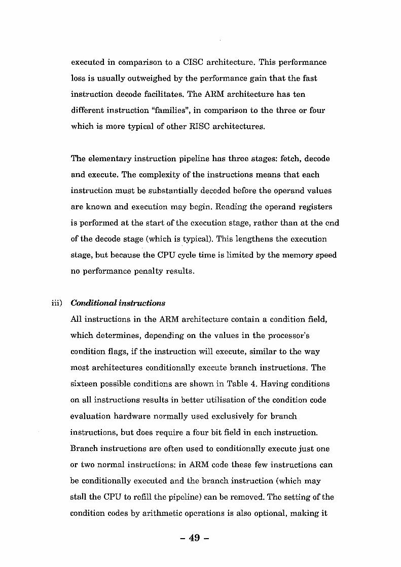
The elementary instruction pipeline has three stages: fetch, decode
and execute. The complexity of the instructions means that each
instruction must be substantially decoded before the operand values
are known and execution may begin. Reading the operand registers
is performed at the start of the execution stage, rather than at the end
of the decode stage (which is typical). This lengthens the execution
stage, but because the CPU cycle time is limited by the memory speed
no performance penalty results.
iii) Conditional instructions
All instructions in the ARM architecture contain a condition field,
which determines, depending on the values in the processor's
condition flags, if the instruction will execute, similar to the way
most architectures conditionally execute branch instructions. The
sixteen possible conditions are shown in Table 4. Having conditions
on all instructions results in better utilisation of the condition code
evaluation hardware normally used exclusively for branch
instructions, but does require a four bit field in each instruction.
Branch instructions are often used to conditionally execute just one
or two normal instructions: in ARM code these few instructions can
be conditionally executed and the branch instruction (which may
stall the CPU to refill the pipeline) can be removed. The setting of the
condition codes by arithmetic operations is also optional, making it
-49-

possible to preserve the condition codes throughout a sequence of
such instructions. Consider the code for a Greatest Common Divisor
algorithm, the C code is to find the GCD of a and b (leaving the result
in both a and b)
while (a != b) if (a >
a else
b
b) -=
-=
b
a
I* reached the end yet ? *I I* if a is greater than b *I I* subtract b from a *I
I* subtract a from b *I
The assembly code for a "normal" architecture would be
gcd cmp beq blt sub bal
bgtra sub bal
end
rl,r2 end bgtra rl,rl,r2 gcd r2,r2,rl gcd
I* reached the end yet ? *I
I* if a is greater than b *I I* subtract b from a *I
I* subtract a from b *I
But the assembly for ARM is
gcd cmp subgt sublt bne
rl,r2 rl,rl,r2 r2,r2,rl gcd
I* if a is greater than b *I I* subtract b from a *I I* subtract a from b *I I* reached the end yet ? *I
These instructions are particularly useful for range checking - the
code for absolute value (of register 1) is
abs cmp rl,O rsbmi rl,rl,O
I* test sign *I I* a:=O-a (two's complement) *I
The code to replace ASCII control code in register 1 with a "?" is
repl cmp r1,127 cmpne rl," "-1 movls rl, '?'
iv) No delayed branches.
I* is it a DEL *I I* or less than space *I I* then replace it *I
Branch instructions take three cycles to execute if they jump to a new
memory address (i.e. if they really do branch, but only take one cycle
if they do not branch). The first of the three cycles is used to execute
the branch instruction, the two remaining cycles are needed to reload
-50-

the instruction pipeline from the branch destination address. To
simplify the processor no instructions are executed while the pipeline
is reloaded (i.e. the instruction after the branch is not executed as a
branch delay instruction). A delayed branch architecture requires
two program counters because a trap can occur in the branch delay
slot as well as in the branch destination; one PC contains the address
of the instruction in the branch delay slot, the other contains the
branch destination address. Of course both program counters must
be saved when a process switch occurs, which as shown later, would
complicate ARM too much to justify the performance gain of delayed
branches, so they are not used. Because ARM has a 26 bit address
bus a condition code, instruction identifier and a complete memory
address can be encoded in a single instruction.
v) Uniform register file.
ARM has twenty-seven general purpose registers, but only sixteen
are visible at once. The remaining registers are mapped across the
processor's four modes of operation: User, Interrupt, Fast Interrupt
and Supervisor, as shown in Figure 4.
-Register 15 contains the program counter, condition code flags and
some processor status bits (Interrupt enable and processor mode).
-Registers 14, called the Link register, is used to store the return
address for subroutine calls.
- Register 13 has no dedicated purpose, but is normally used .as a
stack pointer.
Each processor mode has an individual stack pointer and link
register, and Fast Interrupt mode has five more private registers,
that do not have to be saved between interrupts, which is the main
-51-

reason for this mode's name. Using a general purpose register for
the program counter and status flags has many advantages -
a) the contents may be altered, loaded and saved with existing
instructions and CPU hardware.
b) the condition code settings may be tested with existing
instructions.
c) PC relative addressing modes are easily achieved by using the PC
as the base address register.
d) the entire CPU state is held in general purpose registers, so it can
be saved and restored with ordinary instructions.
User Mode
))I NZCVIF
Condition Codes & Interrupt Status
Program Counter
Interrupt Mode
Fast Supervisor Interrupt Mode
Mode
Figure 4: ARM Register Layout
-52-
Ill
' Processor Mode
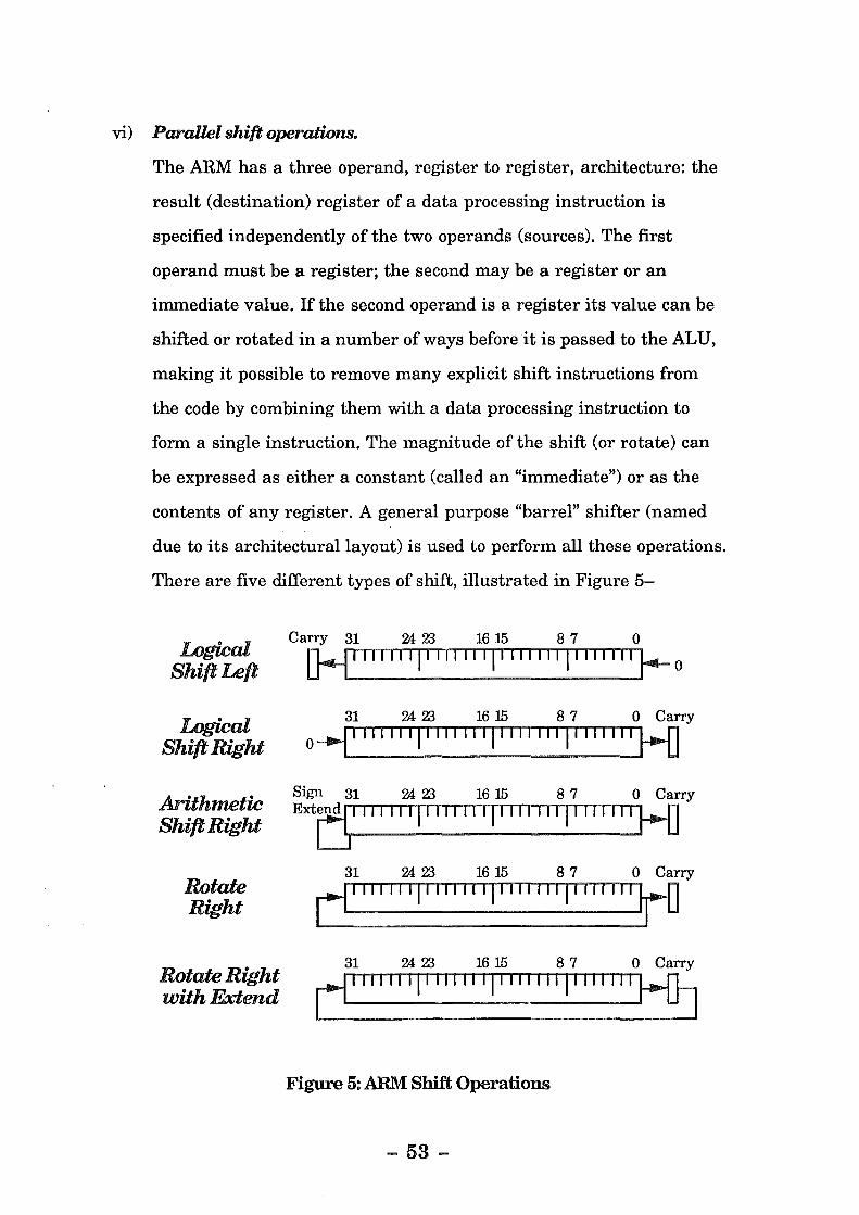
vi) Parallel shift operations.
The ARM has a three operand, register to register, architecture: the
result (destination) register of a data processing instruction is
specified independently of the two operands (sources). The first
operand must be a register; the second may be a register or an
immediate value. If the second operand is a register its value can be
shifted or rotated in a number of ways before it is passed to the ALU,
making it possible to remove many explicit shift instructions from
the code by combining them with a data processing instruction to
form a single instruction. The magnitude of the shift (or rotate) can
be expressed as either a constant (called an "immediate") or as the
contents of any register. A general purpose "barrel" shifter (named
due to its architectural layout) is used to perform all these operations.
There are five different types of shift, illustrated in Figure 5-
Logkal Shift Left
Logkal Shift Right
Arithmetic Shift Right
Rotate Right
Rotate Right with Extend
Carry 31 2A 23 16 15 8 7 0 Q41111111111111111111111111111111 j-.-o
31 2A 23 16 15 8 7 0 Carry
0------11 111 11 111 111 11 111 111 111 11 111 111 H
Sign 31 2A 23 16 15 8 7 0 Carry Ext01111111 11111111 11111111 11111111 H
31 2A 23 16 15 8 7 0 Carry dlllllll!l 1111111111111111111111 'rD
31 2A 23 16 15 8 7 0 Carry dlllllllllllllllllllllllllllllll~
Figure 5: ARM Shift Operations
-53-

a) Logical Shift Left (LSL).
The bits of the operand are shifted left by the specified number of
bits. Zeros are inserted into the right most end of the word, and
the last bit removed from the left most end is placed in the carry
flag. A Logical Shift Left with a magnitude of zero (LSL 0) does
nothing and is the default shift if none is specified.
b) Logical Shift Right (LSR).
The bits of the operand are shifted right by the specified number of
bits. Zeros are inserted into the left most end of the word, and the
last bit removed from the right most end is placed in the carry
flag. An LSR 0 is translated into an LSR 32, to put bit 31 of the
word into the carry flag.
c) Arithmetic Shift Right (ASR).
The bits of the operand are shifted right by the specified number of
bits. The left most bit (the sign bit) is repeatedly inserted into the
left most end of the word, and the last bit removed from the right
most end is placed in the carry flag. An ASR 0 is translated into
an ASR 32, to propagate bit 31 of the word into every bit in the
word as well as the carry flag.
d) Rotate Right (ROR).
The bits of the operand are rotated right by the specified number
of bits. The bit removed from the right most end is inserted into
the left most end of the word, and the last bit removed from the
right most end is placed in the carry flag. A ROR 0 is translated
into a Rotate Right with eXtend (RRX), the carry flag is used as a
33rd bit for the rotate, that is, the right most bit is placed into the
-54-

carry flag and the old value of the carry flag is inserted into the
left-most end of the word. Notice that RRX only rotates by one bit
at a time.
ARM has two extra instructions to fully utilise the "barrel" shifter,
Reverse Subtract (RSB) and Reverse Subtract with Carry (RSC).
These instructions use their operands in the opposite order to the
normal subtraction instructions (SUB and SBC) so that both the first
and the second operand may be shifted or rotated (SUB and SBC
subtract the shifted operand from the unshifted operand, RSB and
RSC subtract the unshifted operand from the shifted operand).
Consider the following ARM code to change the byte order of a 32 bit
word (the word is in rO, rl is used as a scratch register)-
eor rl,rO,rO ror 16 bic rl,rl,OxffOOOO mov rO,rO,ror 8 eor rO,rO,rl lsr 8
The code for a "normal" architecture require 3 more instructions,
and an extra register. The code for constant multiplications is also
very efficient, using only half the number of instructions of a normal
architecture because pairs of shift instructions and add or subtract
instructions can be combined in single instructions.
vii) Rotated Immediate Operands.
The second operand of a data processing instruction may be a
constant (called an "immediate" operand). There are twelve bits
reserved in the instruction for this value, but these bits are split into
two fields: an eight bit quantity and a four bit rotate magnitude. The
eight bit quantity is rotated right by twice the rotate magnitude, using
-55-

the same "barrel" shifter used for shifted register operands. This
allows a more useful range of immediate operand values than a
twelve bit constant, and can be combined with a single instruction as
a bit mask to access all the process status flags in register 15. The
above example used this feature to load a 24 bit constant (OxflOOOO) in
one instruction.
viii) Atypical Addressing Mode Complexity.
The ARM is a von Neumann, load/store (register to register)
architecture. Because the single memory bus is almost fully utilised
loading instructions, the load and store instructions must take more
than one cycle (one to load a new instruction and another to access
memory for the load and store). Because the cycle time of ARM is
limited by the access speed of memory, loading data will take a full
cycle, and a third cycle will be required for load operations to transfer
the loaded data from the data bus to the destination register. However
this third cycle is usually overlapped with the next instruction, so
can usually be ignored. Because of the free processor cycle that
occurs before memory can be accessed by a load or store (because an
instruction is being fetched), a rich set of memory addressing modes
have been implemented-
a) Base Register plus Offset.
The value of a base register and an immediate value or the value
in an offset register are combined to form the memory address.
The immediate is a twelve bit unsigned integer which may be
added or subtracted from the base register (effectively yielding a
thirteen bit signed immediate offset). The value of the offset
register may be shifted in a similar manner to the second
-56-

operand of a data processing instruction, (although only by an
immediate amount).
b) Base Register Plus Offset with Pre Increment (or Decrement).
These modes are similar to Base Register plus Offset, but the
result of the base register and offset addition (or subtraction) is
written back to the base register. This mode is useful for
accessing arrays of data. The shift applied to a register offset can
be used to directly scale the array index.
c) Base Register Plus Offset with Post Increment (or Decrement).
These modes are similar to the above except the Base plus offset
calculation is not performed or written back to, until after the
memory access has been made. These modes are also useful for
(scaled) array operations.
It should be noted that these addressing mode calculations only use
existing hardware used for normal addition and subtraction data
processing instructions, so they only add decoding hardware to an
implementation. A flag in the instruction word indicates that a
single byte should be loaded from memory rather than a full word;
there is no single instruction to load a 16 bit quantity or to load and
sign extend a byte.
ix) Multiple register operations.
Two instructions are provided to load and store multiple registers to
and from memory. Any or all of the sixteen registers visible in the
current processor mode can be loaded or stored with one (multi
cycle) instruction. Similar addressing modes to the single register
-57-
loads and stores can be used for these multiple register operations,
providing very efficient stack and queue operations. These
instructions also inform the memory system that data will be loaded
sequentially, so the fast DRAM page mode memory accesses can be
used. This makes these instructions nearly four times more efficient
than separate load/store instructions, because the latter must load as
many instructions as data objects (which will take twice as long) and
cannot utilise the page mode DRAM accesses because instructions
and data are accessed alternately (and page mode cycles are twice as
fast as normal cycles).
Because the entire CPU context for each processor mode is held in
the sixteen visible registers, procedure calls and context switches are
very efficient. For example, the entry sequence to a procedure might
save all the registers on the stack (pointed to by r13) with
stmfd r13!,r0-r14
and the exit sequence might return with
ldmfd r13!,r0-r13,r15
The f and d indicate the type of stack: "f' for full - the stack pointer
points to the next value to be popped from the stack ("e" for empty
would mean the stack pointer points to the location where the next
push will put its data) ; "d" (descending) indicates the direction of
stack growth, its opposite is "a" (ascending). The "!" indicates the
stack pointer (in this case r13) should be updated with the new top of
stack value. Notice these two instructions also generate the
procedure return by saving the value in the link register and loading
it back as the program counter.
-58-

x) Software Interrupt.
This instruction causes the processor to switch to supervisor mode
and jump to a fixed address, to provide an entry point into the
operating system from a program. A 24 bit field in the instruction is
used to specify the Operating System function that is required.
xi) Coprocessor interface.
The ARM instruction set includes three instruction families to
manage an efficient interface for hardware co-processors, which
add hardware support to the ARM architecture. Up to sixteen co
processors can be connected to the interface at once, for example a
Floating Point Unit, graphics accelerator or digital sound processor.
The three instruction families are-
a) Co-processor data processing.
This class of instructions is used to inform a co-processor that it
should perform some internal operation, such as a "floating point
addition" in the case of an FPU. The instruction specifies two
source registers and a destination register for the operation, and
may specify up to 128 different operations.
b) Co-processor register transfer.
These instructions are similar to the above class, except that they
specify a single ARM register. This is useful for operations like
"convert integer to floating point", the integer is held in an ARM
register, and the result of the conversion is placed in an FPU
register.
-59-

c) Co-processor load/ store data.
These two instructions are used to load data from memory into a
co-processor register. The ARM CPU handles all the address
calculations and has the same addressing modes as the normal
load and store instructions, except the immediate offset can only
occupy eight bits instead of the normal twelve (the other four are
used to specify the co-processor number).
xii) ARM 3 Cache.
The ARM3 implementation has a small cache memory on the same
chip as the CPU (it also has a semaphore instruction to aid systems
with multiple CPUs). The cache holds four kilobytes of instructions
and data, is 64 way set associative, with a sixteen byte line size and a
write through random replacement algorithm. It uses virtual
addresses because the address translation hardware is not included
on the CPU chip. The cache controller is configured as a co
processor for simple programming. The cache does not have a write
buffer: when a store instruction is executed the CPU clock is
synchronized with the main memory clock, and the instructions
proceed at the main memory speed. Adding a write buffer to the
cache would alter the exception handling mechanism, making
ARM3 incompatible with ARM2.
The hnpact on Performance
An approximation of the effect that these architectural features have on
the overall performance of ARM can be quantified using known statistics
for the relative frequencies machine code instructions [Gros88] [Tane78].
-60-

If ARM had delayed branches to optimise "taken" branch performance,
two delay slots would be required. Compilers for architectures with two
delay slots can fill around sixty percent of the delay slots with a useful
instruction, and taken branch instructions for these architectures are
responsible for about twelve percent of all instructions, so ARM loses
12% of instructions x 2 delay slots x 60% filled slots
or about fifteen percent of its performance because of the lack of delayed
branches. About fifty percent of branch instructions branch around just
one instruction, a further twenty percent branch around just two: these
branches can be replaced by ARM's conditional instructions. The time
taken (number of cycles) for an ordinary branch around one or two
instructions in ARM is approximately
50% x 3 cycles for a taken branch+ 50% x (1 cycle untaken branch+
70% x 1 instruction + 30% x 2 instructions)
or about 2.6 cycles on average. Using conditional instructions the number
of cycles drops to
70% x 1 instruction + 30% x 2 instructions
or just 1.3 cycles, resulting in a 65 percent increase in the efficiency of
branch instructions, or an overall loss over delayed branches of twelve
·percent.
Shift operations account for approximately five percent of all instructions.
Many of these can be performed in parallel with data processing
instructions, say eighty percent, a net saving of about four percent of all
instructions. The barrel shifter lengthens the critical CPU data path by
about fifteen percent, but the access time of the main memory is still
longer than the time spent in the execution stage, so this fifteen percent
has no effect on the overall performance.
-61-

The single register transfer instructions have a useful set of addressing
modes not usually found on RISC machines, and these should yield an
eight percent performance gain. The multiple register transfer
instructions can be used for efficient procedure calls and data block move
operations and are used for about half of all memory accesses [Furb89]
(about twenty percent of all instructions), making them very worthwhile
as they make DRAM memory accesses nearly four times more efficient,
and would be expected to yield a twelve percent performance increase.
Because the program counter is a general purpose register, jump
destinations that are evaluated at run time (as in a CASE statement) can be
efficiently handled with general purpose instructions, but the frequency of
CASE statements is too low for this to add a significant performance
advantage.
Thus when ARM is connected to DRAM a twelve percent performance
increase would be expected over a simpler machine (say the MIPS
architecture). When connected to SRAM (or a cache) the fifteen percent
longer cycle time and the lessening in the usefulness of the multiple
register transfer instructions would make ARM roughly equivalent to a
·more simple architecture.
Thus the ARM architecture has efficient support for all the high level
language features listed in Chapter 2. A highly optimised text
decompression algorithm written using many of these features can
decompress data faster than traditional architectures (both CISC and
RISC) [Jagg89]. The above features can be fully exploited by a high level
language compiler resulting in a very desirable computer: one with a low
price/performance ratio.
-62-

Evaluating an architecture
Evaluating a new architecture is a task made up of several stages -
i) Programs must be chosen as performance benchmarks, to evaluate
the architecture. The emphasis here has been on utility programs
from the UNIX Operating System, written in the C programming
language.
ii) A compiler, its associated optimisers, an assembler and a linker
must be built to transform the high level code of the benchmark
programs into efficient executable machine code. The ability of the
compiler to produce good code is relied upon by RISC architectures to
gain good performance, as detailed in Chapters 4 and 5.
iii) A performance monitor must be constructed, firstly to evaluate the
quality of the code produced by the compiler, and secondly to evaluate
the ability of the architecture to support the high level language
features, as detailed in Chapter 6.
All these tasks have been successfully completed for the evaluation of the
ARM architecture. An optimising compiler has been constructed to
·exploit the ARM architecture to produce efficient code, rather than being
"user friendly" enough to release as a commercial product. A software
performance monitor has been built to record accurate information on any
architectural feature, whilst still providing good performance so that it
could be used to evaluate the execution large programs. The benchmark
programs chosen were designed to give a reliable estimate of performance
for the type of code that the ARM architecture could execute, as described
in Chapter 7.
-63-

Chapter4 Computer Software
The Operating System, compilers and application programs that use the
computer hardware are responsible for delivering the performance to the
user. Inefficient algorithms can neutralise the performance of the fastest
CPU, and inefficient data structures can devour precious memory.
The Operating System
The Operating System (OS) of a computer is a unique program used to
allocate the computer's resources, such as the CPU, memory and disk
drives. Designing an OS from scratch is a very long and expensive
undertaking. UNIX™ is becoming a standard Operating System for high
performance microcomputers (workstations), due to its portability
between different types of hardware. The main reason for this portability
is because UNIX is almost entirely written inC, a high level language. A
small machine code kernel of low level operations, and a C compiler is the
only software that is required for UNIX to be ported to a new machine (a
· crude method of loading the initial kernel and compiler into the machine
(called a "bootstrap") will also be required). Clearly the machine code
kernel must make efficient use of the low level resources it allocates,
because the rest of the OS relies on this code. Even more importantly, the
C compiler must produce very efficient code to fully utilise the computer
hardware, as most of the Operating System is compiled C code.
-64-

Compilers
High level languages are used to construct Operating Systems and
application programs. For a compiler to be effective, it must produce
machine code of comparable quality to machine code that is hand written
by a programmer. Constructing complete compilers for a range of
programming languages for a new machine is an extremely labour
intensive operation, so compilers are usually split into two parts, called
the front-end and the back-end. A different front-end is constructed for
each high level language, to transform the high level language code into
an "intermediate" code, which has a semantic level somewhere between
high level languages and a computer's machine code. One back-end is
made for every different architecture, it takes the intermediate code
produced by a front-end and transforms it into machine code. Careful
selection of the statements or instructions in the intermediate code allows
it to be used for a number of similar language front ends (C and Pascal for
example), and be translated by a number of back-ends into the machine
code of different architectures. Intermediate languages tend to be simple,
and general purpose, in fact very similar to RISC code, for two reasons-
a) The intermediate code does not need to have an efficient bit level
encoding (like assembly code), so, for instance, the size and number
of intermediate instruction operands are not limited by the size of a
certain instruction format.
b) It is much easier to construct a compiler for a simple instruction set
than for a complex one, which is one reason for the development of
RISC machines. Sequences of simple instructions offer more
opportunities for optimisation than compound complex instructions.
-65-
The back-end for a CISC architecture is much more complex than a
RISC back-end, because its main task is to replace a sequence of simple
intermediate code instructions with a complex one. The RISC back-end
has a more simple task: the job of producing RISC assembly from
intermediate code can be reduced to little more than a translation if the
intermediate code is properly selected. This allows more time for
optimisation of the intermediate code, generating a direct code
improvement to the final assembly code.
So to produce a new compiler for a different high level language only
requires the construction of the front-end, and the language becomes
available on all machines with a suitable back-end. To port existing
compilers to a different architecture only requires the construction of a
back-end, which is then combined with each front-end, to produce
compilers for a range of high level languages. This is far more efficient
than constructing complete compilers for every language on every
machine. The extra level of translation required by using an intermediate
language seems theoretically inefficient, but because the total workload
·has been roughly halved (to support a new language or new architecture),
more effort can be expended on the remaining work, culminating in an
superior compiler produced in the same time span [Aho86].
Figure 6 illustrates the translation path from high level language code to
intermediate code to machine code. Both the front-end and the back-end
are split into a number of separate sections -
-66-

Front End
Back End
Figure 6: Compiler Stages
i) Language Pre-processor.
The C programming language has a pre-processor to expand
macros (defined with #define), textually include files in a program
(#include), and conditionally compile high level code (#ifdef).
ii) Intermediate Code Generator.
The code generator in the front-end is responsible for translating
each high level language statement into one or more intermediate
language statements or instructions by parsing the high level
language symbol by symbol (a symbol is a syntactic atom) and
generating suitable intermediate code to carry out the action
required. For example an IF statement will be translated into code to
evaluate the Boolean expression controlling the IF, and the result of
the Boolean expression will be used as the condition on a branch
instruction to the end of the body of the IF statement. In fact the
evaluation of expressions is often the most complex part of the code
-67-

generator, due to operator precedence and context requirements. The
allocation of variables to CPU registers (register allocation) is
planned here, by inserting temporary information into the code about
variable usage frequencies. For a full description of code generation
see [Aho86].
iii) Intermediate Code Peephole Optimiser.
This section of the front-end scans the code produced by the code
generator looking for short sequences of instructions that can be
replaced by shorter or more efficient sequences. Such sequences are
often found on the boundaries between code produced by different
sections of the code generator: for example, the boolean expression
evaluator may finish by pushing its return value onto a stack, and
the code produced for an IF statement may begin by popping the value
of the stack, these push and the pop operations can be removed to
funnel the boolean value straight to the branch instruction produced
for the IF statement.
iv) Intermediate Code Global Optimiser.
This section of the front-end is responsible for manipulating entire
blocks of code, to make them more efficient. Many global
optimisations are possible, especially with a simple intermediate
code-
a) Common Sub-expression Elimination.
Multiple computations of the same expression are removed by
this phase. The result of the first computation is stored in a
temporary location and the second computation is replaced by a
reference to this location. Of course extreme care must be taken to
-68-

ensure the value return by two expression evaluations are indeed
the same (function calls complicate this due to global information
that may affect the result).
b) Strength Reduction.
The evaluation of expressions using loop variables is called
strength reduction. Expressions involving loop variables create
arithmetically progressive results that can be simplified, to
produce faster calculation methods.
c) In-line Substitution.
Procedures and functions that are called only once may be shifted
into the main stream code and the corresponding call and return
statements removed. The body of the procedure or function may
need to be modified to save the contents of registers used in the
procedure. This optimisation can be used on procedures that are
called more than once, but this will lower cache performance
because the multiple copies of a procedure body will be cached
separately.
d) Stack Pollution.
After a procedure call the arguments passed to the procedure
must be removed by the caller. When procedure calls happen
frequently, cleaning up the stack after each individual call may be
deferred, to allow several clean ups to be combined into one.
e) Copy Propagation.
Statements of the form A := B (in Pascal) can be removed, and all
-69-

subsequent references to A replaced by references to B, provided
that the values of A and B do not change.
f) Constant Propagation.
Statements of the form A := constant (in Pascal) can be removed,
and all subsequent references to A replaced by references to the
constant, provided the value of A does not change.
g) Cross Jumping or Tail Merging.
Two bodies of code that end by jumping to the same location, and
have the same statements before the jump may share one copy of
these statements by inserting a jump instruction before one
sequence to jump into the beginning of the other. Duplication of
statements often occurs in the code following an IF statement and
the code after the corresponding ELSE.
h) Loop Unrolling.
Unrolling loops involves joining several copies of the loop body
together to lower the number of jumps to the beginning of the
loop. This optimisation is only practicable for very short loop
bodies - it increases code size which reduces cache efficiency.
i) Code hoisting.
Calculations that are invariant in a loop may be shifted to before
the loop where they will not be repeatedly evaluated. The major
index calculation used in matrix operations is a classic target for
code hoisting.
-70-

j) Loop fusion and loop splitting.
Loops may be split into separate loops, to allow other
optimisations (such as code hoisting, unrolling and strength
reduction). Two loops may also be joined to remove repeated
looping constructs over the same range.
k) Dead code elimination.
Many of the previous optimisations can leave code that is never
executed (especially constant propagation, copy propagation and
cross jumping), which is removed by this phase. Calculations
yielding results that are never used are also removed by this
phase.
1) Register allocation.
Making efficient use of CPU registers to hold frequently used data
is probably the most important optimisation. The register
allocation phase in the front end provides broad hints to the back
end as to which variables are best placed in registers. Local
variables, procedure arguments, global variables and procedure
identifiers are common candidates for register allocation.
Pointers, record fields and individual array elements can be
stored in registers, but the algorithms required to do so are very
complex. The allocation of variables to registers can be considered
as a graph colouring problem (as it is a time-tabling application),
where each node of the graph represents a variable, and a path
between nodes indicates that those variables are in use ("alive") at
the same time. The colouring algorithm attempts to colour the
graph, the number of colours that can be used is dictated by the
number of available registers. When a graph cannot be coloured
- 71-

some nodes must be removed, this means saving register
contents to memory (register "spilling"), a set of heuristics are
used to decide the best register to spill. Although colouring
algorithms are NP complete, they may be supplemented with
heuristics to make their use practicable in a compiler
[Brig89,Chat81, Chat82, Chow84, Chow88].
The optimisation passes of the compiler are usually controlled by
options to activate them. During program development the extra time
required for code optimisation is wasted, and in the extreme the
subsequent reorganisation of code makes source level debugging very
difficult. The optimiser is usually only used late in the software
development cycle, hence the discretionary use by the programmer.
v) Machine Code Generator.
A second code generation stage in the back-end is used to transform
the intermediate code into machine code mnemonics - assembly
code. This code generator must make efficient use of the particular
machine architecture, by efficiently utilising its instructions and
addressing modes. The final stage of register allocation is done here
(the actual graph colouring algorithm using information passed
from the front end). It is this stage of the compiler that benefits the
most from a RISC architecture due to the reduction in the number of
possible code sequences that can be generated.
vi) Machine Code Peephole Optimiser.
Another peephole optimiser pass can be used in the back-end to
remove any inefficient machine instruction sequences produced by
the machine code generator. This may involve combining load and
-72-

add instructions into a load with auto increment instruction.
Compare instructions can often be removed if the processor flags can
be set automatically by a preceding calculation. If the intermediate
code is carefully chosen, very little optimisation should be required
here, as the code generator should not generate sub-optimal
sequences of assembly instructions for optimal sequences of
intermediate language instruction. Again a RISC architecture helps
here, as the choice of instructions to generate is very limited
(compared to a CISC), and it therefore benefits more from the front
end optimisations, because optimisation are not un-done by
inefficient CISC instructions (with wasted side effects). Optimal
sequencing of instructions and data can be made here, to optimise
the effectiveness of cache algorithms.
vii) Assembler and Linker.
Although not really part of the compiler, the final stage of the back
end (and the entire compilation process) transforms the mnemonic
assembly language into machine code. For every assembly language
instruction there is exactly one machine code instruction, so no
further optimisation will be required to select the most efficient code
sequences. The linker combines multiple files together to produce an
executable image, by resolving references between different parts of a
program compiled at different times, and references to any language
library functions.
An intermediate language allows a common back-end to be used for
similar languages (for example Pascal, Modula 2, C and Algol), the
emphasis for better optimisation can be focused on a common optimiser
for the intermediate language to be used with all front-ends, and
-73-
optimiser for a particular architecture (or even individual
implementations).
Application Programs
The algorithms used by application programmers have a far greater effect
on the performance delivered to the computer user than compiler
optimisation. It is common practice for programmers to optimise their
high level code for a particular architecture and implementation. This
practice is only suitable for code dedicated to that machine, any less
specific code should be written without programming "tricks" as these
only confuse the compiler and hinder its optimising ability. Consider the
following C code sequences to swap two integer variables -
(a)
inti , j ;
i:iAj;
j:iAj;
i:iAj;
(b)
inti ,j, temp;
temp= i;
i = j;
j =temp;
Code sequence (a) uses the exclusive-or operator to swap the value ofi and
j, sequence (b) uses a temporary variable. Code (a) may be more efficient
because it uses one less variable (which will probably equate to a register),
but a copy propagation optimisation pass will usually remove code
sequence (b) from the code, and merely swap all following references to i
and j. The low level optimisation of programs is better left to the compiler,
the programmer should endeavour to find more efficient algorithms and
data structures to build efficient programs, and turn on full optimisation
late in the development cycle. If for some reason the resulting code is
-74-

inefficient the compilation process may be halted (with a compiler switch)
before the assembler pass, the critical parts of the code altered (or
completely rewritten) by hand, and the code then assembled and linked as
before.
-75-

ChapterS An Optimising Compiler for ARM
The most important piece of software in a high performance computer
system is the compiler, to deliver the maximum hardware performance to
the end user. The hardware can assist the compiler by making many
optimisations possible, which is the reason for the development of RISC,
but a fully optimising compiler for any architecture is a major software
project.
The C language is widely renowned for efficient compilation and
opportunity for optimisation [Kern78], and has been chosen here as the
high level language to be compiled and optimised. Modula 2 and more
lately Oberon have proven to be languages with similar compiler efficiency
to C [Wirt88, Wirt89].
Compiler Building Tools
Four different approaches were investigated for the construction of a fully
optimising C compiler for ARM -
i) Hand crafted compiler and optimiser.
Given enough time, this approach will result in the best compiler.
An intermediate language could be tailored especially for ARM, to
make a common intermediate language for many language front
ends, allowing the same optimisers and back-end to be used for each
front-end. MIPS Computers used this approach to build the best
commercially available production optimising compilers [Morr88].
-76-

Unfortunately the amount of work required by such a compiler is too
great to be practicable here.
ii) The Portable C Compiler.
The Portable C Compiler (PCC) is a two pass C compiler with a
mixed intermediate code of both assembly code (for control
structures) and tree structures (for expressions). The first pass is
almost machine independent, performing some simple optimisations
on expression trees (constant propagation and strength reduction).
The second pass generates assembly code from the expression trees,
using a technique developed by Sethi and Ullman [Aho86] to produce
efficient code. Porting PCC to a new architecture requires from two to
five thousand lines of the code be written, as well as the code for a
machine dependant peephole optimiser, but high quality compilers
can be produced. Many commercial compilers are based on PCC,
including Acorn's ARM C Compiler.
iii) The GNU C Compiler.
The GNU C Compiler (GCC), from the Free Software Foundation, is
made up from a collection of C programs. Some simple optimisations
are applied to the intermediate code (called Register Transfer
Language, or RTL), and are thus machine independent. Porting the
compiler to a new architecture requires three main files be written:
an instruction output file, a machine description file (architectural
description) and a target description file (implementation
description). Together these files contain between two thousand and
six thousand lines of C code (depending on the target machine). GCC
has been ported to all common architectures: DEC VAX, Motorola
-77-

680x0 and 88000, Intel80x86 and 80860, SUN SPARC, MIPS and
National's 32000 series, and to many more obscure architectures.
iv) The Amsterdam Compiler Kit.
The Amsterdam Compiler Kit (ACK) is the most extensive compiler
building tool available, providing tools to construct all the parts of a
compiler described in Chapter 4: pre-processor; front-end code
generator; peephole optimiser; global optimiser; back-end code
generator; back end peephole optimiser; assembler and linker
[Tane83a]. An intermediate language, called EM code, is generated
by the front-end from a high level language, and transformed into
machine code by the back-end [Tane83b]. The same pre-processor
and front-end optimisers are used by all compilers built with the kit.
Porting the compiler to a new architecture requires between two
thousand and five thousand lines of source code (not C) be written.
Front-ends currently exist for C, Pascal, Modula 2, Basic, Occam
and Ada, with a front-end for Algol 60 under development. Back
ends exist for DEC PDPll and VAX, Intel80x86, Motorola 680x0,
National32000, MOS Technology 6502 and Zilog Z80 architectures.
The choice of compiler building tool was based on three criteria -
i) Suitability of ARM as a target.
All three compiler kits meet this requirement, for different reasons.
PCC must be suitable, as a PCC based compiler already exists for
ARM. GCC has been targeted to several other RISC machines, with
similar architectures to ARM, and because the flexibility of C can be
utilised when building the back-end, it could almost certainly exploit
the special features of the ARM architecture. ACK's intermediate
-78-

language (EM code) is similar to ARM code (in fact there is a one to
one relationship between many EM instructions and ARM
instructions), but the source language used is rather restrictive, and
may not be able to exploit all the special features of ARM.
ii) Work required to build a compiler.
The original goal of a low cost, high performance compiler must be
met, which is why hand crafting compiler is not possible. PCC
requires significantly more work than either GCC or ACK, because
of the lack of machine independent optimisation (a separate peephole
optimiser needs to be written from scratch). GCC porting requires a
large amount of C code to be written, and while this is very flexible,
the source code for ACK is substantially easier to use (because its
source code was specifically designed for compiler building).
iii) Quality of source code.
Of course the compiler must be able to utilise the ARM architecture.
The Acorn PCC based compiler produces reasonable code, but hand
inspection showed there are many ways in which it could be
improved. By comparing code produced by GCC and ACK for the
Motorola 68000, some insight of their code generation ability is
gained. Without optimisation both GCC and ACK produce similar
quality, similar length code, but when ACK's powerful global and
peephole optimisers are enabled [Bal85, Bal86, McKe89], very high
quality code is produced.
These three factors indicated that ACK would be the most suitable tool to
use, as long as it could be made to generate code that exploits the special
features of the ARM architecture.
-79-

EM code and the Code Generator Generator
EM code, ACK's intermediate code as shown in Appendix B, is a low level
intermediate language. The result of using this low level code is that EM
is only targetable to architectures with certain qualities. The most
important is that each byte in the memory must have a unique address.
EM is a stack based intermediate code, instructions like adi (add integer)
pop two operands from the stack and push the result back on the stack.
EM has several built-in data types: signed and unsigned integer, floating
point numbers, pointers and sets of bits. There are no general purpose
registers - local variables and arguments are addressed via an offset from
the stack frame. There are, however, a few special purpose registers: a
Program Counter, a Local Base (which points to the start of local
variables), a Stack Pointer and a Heap Pointer.
ARM will be the first RISC architecture that ACK has been targeted to.
The strict requirement of RISC architectures for powerful optimising
compilers will test the ability of ACK front-ends to produce good code, any
imperfections will be clear as poor sequences of ARM code will be
translated from poor EM code (poor sequences of CISC code could be
caused by the complex task performed by the CISC code generator). It is
therefore worth examining how the features of ACK can be utilised to
produce a high quality RISC compiler.
The Code Generator Generator (CGG) program uses an architecture
description table to build a code generator for a new architecture. This
description table must be written to produce a back-end for a new
architecture (for example ARM). The description table uses an
-80-
architecture description language to describe the target architecture,
made up of a number of sections -
i) Constant declarations.
Constant values are defined at the beginning of the table, and may be
used throughout the rest of the table. The C pre-processor is used for
an initial pass over the table, so pre-processor constants and macros
can also be defined here. Constants like the size of a stack frame, and
macros to perform range checking on operands are defined here.
ii) Register properties.
The properties to differentiate between different target register
classes are defined in the table. Registers are allocated later in the
table by requesting a register with a property, and the register
allocator will choose the best register with that property. The ARM
table has two main register properties: REG which includes all ARM
registers and ALLOC which are the registers used for temporary
allocation.
· iii) Register definitions.
The properties of each target register are defined in this section,
including the name to be used in the assembly code and the registers
that are available to hold program variables (as opposed to "scratch"
registers, used to hold temporary program values). The ARM table
uses registers zero to six as scratch registers, and registers seven to
eleven as register variables. Register twelve is the Local Base (LB),
register thirteen is the Stack Pointer, register fourteen is the Link
Register and a code generator scratch register, and register fifteen is
the Program Counter.
- 81-
iv) Token definitions.
The types of all instruction operands (called "tokens") are described
in this section. The attributes of each token (for instances base
register and integer offset for a simple addressing mode) are defined,
including their size, type and assembly language output format. The
types of tokens are addresses, integers and all the register properties.
A "cost" value is given to each token, to inform the code generator
about the space and execution time cost of using this operand. The
code generator uses these costs to make the best choice between
multiple token possibilities when generating instructions, and can be
tuned to produce code with a desired balance between code size and
execution speed. The ARM table uses a large number of different
tokens, many of which are designed to utilise ARM's unusual twelve
bit immediate format used with data processing instructions. The
different types of shifted register operands for data processing
instructions are also handled here, along with many base plus
register addressing mode formats. A special token (called bigconst)
has no corresponding ARM operand type, it is used to manipulate a
constant that will not fit in an ARM immediate field. Three extra
pseudo instructions have been added to the assembler to find the
optimal way to actually move, add and subtract a bigconst to a
register value (which in practice involves up to four real ARM
instructions). Just which instruction operand should be defined as a
separate token is certainly not obvious, conversions and comparisons
between different tokens are used later in the table, and the
relationships between tokens is not obvious until they are required
later.
-82-

v) Token sets.
A number of different tokens can be grouped to form a set, to describe
all the operands of one instruction in a compact manner, for example
a load instruction will have several legal addressing modes (tokens)
as one operand, and so all the legal addressing modes for a load will
be grouped into one set. The large number of tokens in the ARM table
are grouped into just a few token sets, for constants, registers, data
processing operands (which are constants, registers and shifted
registers) and addressing modes.
vi) Instruction definitions.
Each instruction in the target architecture is defined in this section,
along with its assembly language output format and its operands
(token sets). Each operand is qualified as read only, read and write or
write only, so that that code generator can tell if the value of an
operand will change. Operands whose value is used to update the
condition flags are marked here also. The instructions also have a
cost field so the compiler can calculate the best code sequence when a
choice is available. The ARM architecture has a potentially large
instruction set, due to the sixteen different conditions that can be
applied to each instruction, far too many combinations of instruction
and condition code to be declared here. The instruction conditions are
not sufficiently like operands to be simply declared as tokens. To solve
this problem new pseudo instructions have been created, called IF,
and sixteen IF instructions have been declared, one with each
condition code. Extra functionality has been added to the assembler to
merge an IF statement's condition with the following instruction, to
make it conditional. This technique makes some patterns a little
longer, but with proper indentation, quite readable. All sixteen types
-83-

of branch are defined explicitly, because each type is used frequently
later. All ARM's data processing instructions had to be defined
twice, once for the version that automatically sets the condition codes,
the other for the ordinary version. Some special pseudo instructions
have been added to manipulate the bigconst token, which is used to
manipulate integers that cannot be encoded in ARM's instructions,
and for integers whose size is unknown at compile time (which are
all actually addresses).
vii) Move definitions.
This part of the table defines the instructions needed to move data
from one place to another, for instance, a load instruction will exist to
load data from an address into a general register. Moves are handled
specially because they enable the code generator to keep track of
register contents. The ARM table has move operations to load a
register with all token types declared in the token section.
viii) Test definitions.
Setting the processor status flags is also handled specially, as some
instructions may do this automatically (as defined in the instruction
definitions), so instructions to explicitly set flags can often be avoided.
The code generator remembers the value that was last used to set the
status flags to decide when explicit condition code setting
instructions are required. The only test rules in the ARM table test a
register and a constant, or two registers.
ix) Stacking Rules.
These rules define how to store the value of a token on the stack. The
-84-

table must contain a stacking rule for every token. Tokens are
usually only pushed on the stack before procedure calls.
x) Coercions.
These rules define how to remove tokens from the stack, and how to
convert between different token types. These ru1es are used to
massage data of different types into the correct type for use with an
instruction. All ARM's coercions are used to move tokens into
registers (and to pop tokens off the stack after procedure calls).
xi) Code patterns.
This is the largest, and most important section in the code generator.
It describes the target instructions that should be generated for each
EM instruction. There is usually a different code sequence depending
on the contents of the stack (i.e. depending on the types of the
instruction operands). Registers may be automatically allocated and
initialised in each pattern, and any result that should be left on the
stack after the instruction has executed is also defined here. The
patterns in the ARM table are quite straight forward, most having
only a few alternates. Take for example the EM add integer (adi)
instruction, which has the following pattern -
pat adi $1==4 with REG regconst uses reusing %1, reusing %2, ALLOC gen add %a,%1,%2 yields %a with regconst REG uses reusing %1, reusing %2, ALLOC gen add %a,%2,%1 yields %a with REG negconst uses reusing %1, reusing %2, ALLOC gen add %a,%2, {onlyposconst,0-%1.num} yields %a
-85-

The first line (pat adi $1==4) declares the EM pattern to be matched
(adi) and checks that the size of the argument ($1==4) is the word
size. The second line (with REG regconst) is a stack contents
constraint: if the top of stack contains a register, and the next stack
location is a register or a constant, then this rule may be used. The
third line (uses reusing %1, reusing %2, ALLOC) allocates a register
of type ALLOC, and states that any registers used in the top of stack
token (%1) or the next stack token (%2) may be reused for this
allocation. The fourth line (gen add %a,%1,%2) defines the ARM
instruction that should be generated (add register %1 to register or
constant %2 and store the result in the newly allocated register %a).
The fifth line defines the result to be placed back on the stack, the
result register, %a. The next four lines produce similar code when
the operands are in the opposite order on the stack, and the last four
lines generate a subtract instruction if the constant is negative. The
expression {onlyposconst,0-%1.num} converts the negative constant
token value into a positive constant token value.
Code patterns may match a string of EM instructions, for instance a
load followed by an increment of the load instruction base register
can be combined into an auto-incrementing addressing mode. The
complex addressing modes of the ARM architecture are easily
catered for here (in fact ARM's addressing modes are quite simple
compared to the CISC addressing modes CGG was designed to
handle). Long sequences of ARM code may also be produced by the
code generator, for example the pattern for an EM divide instruction
is quite long (as shown in Figure 7) because the ARM does not have a
divide instruction. This divide routine is used in two variations: as
in-line code to be inserted directly into the generated code every time
-86-

a divide instruction is used (for speed efficiency) and as the body of a
library routine, called as a subroutine every time a divide instruction
is used (for space efficiency). Each use has different a cost
declaration, so the code generator chooses the most appropriate
method. To divide the integer M by integer N takes 25 cycles if N is
greater than or equal to M and
Olog2Ml- llog2N + 11) x 14 + 11
cycles ifM is greater than N. This algorithm could be made even·
faster (the multiplier of 14 would become 10) by unrolling the two
loops, but the code becomes so long that cache efficiency would suffer
too much for this approach to be effective.
pat dvi $1==4 with REG REG uses ALLOC,ALLOC,ALLOC gen eor %c,%2,%1
movs %a,%2 ifmi .
rsb %2,%2, {zeroconst,O} teq %1, {zeroconst,O} ifmi .
rsb %1,%1, {zeroconst,O} mov %b, {onlyposconst,1}
1: cmp %1,%2 ifcc .
mov %1, {lslconst,%1,1} ifcc .
mov %b, {lslconst,%b,1} brcc {label,1b} mov %a, {zeroconst,O}
2: cmp %2,%1 ifcs .
sub %2,%2,%1 ifcs .
add %a,%a,%b movs %b, {lsrconst,%b,1} ifne .
mov %1, {lsrconst,%1,1} brne {label,2b} teq %c,{zeroconst,O} ifmi .
rsb %a,%a, {zeroconst,O} yields %a
Figure 7: ARM Signed Divide Routine
-87-
Integer divisions can also be handled by converting the integer
operands to Floating Point format, performing the divide in the
Floating Point Unit, and converting the result back to integer. This
option is only used if a Floating Point Unit is attached.
Two other files must be written to form a complete code generator, mach.h
and mach.c. The former consists mainly of output routines for integers
and labels in the assembly code, the latter has some short routines to
generate the code for procedure calls and returns. These code sequences
utilise the ARM multiple register load and save instructions to save and
restore registers around procedure calls. The procedure entry sequence is
stmdb sp,lb,sp,link sub lb,sp,12 sub sp,sp,num locals+12
The first instruction stores the Local Base, Stack Pointer and Link
Register on the stack. The second instruction resets the Local Base to point
to the new procedure's local variable storage, and the third instruction
allocates stack space for the local variables. This sequence takes six clock
cycles. The procedure return statement is just
ldmia lb,lb,sp,pc
which reloads the Local Base, Stack Pointer and Program Counter from
the values stored by the entry sequence, also taking six clock cycles.
Loading the Program Counter from the stored Link Register value
actually makes the subroutine return.
-88-

Global and Peephole Optimisers
The Amsterdam Compiler Kit includes a global optimiser, and a peephole
optimiser. Both these optimisers operate on the EM code produced by the
front-end, and are therefore almost language and machine independent.
The global optimiser does need some knowledge of the target architecture,
mainly for register allocation (such as the number of registers available
and the space and time savings that registers can provide). The global
optimiser performs all of the optimisations discussed in Chapter 4, except
code hoisting, loop fusion and loop splitting [Bal85, Bal86].
The peephole optimiser replaces short sequences of EM instructions with
better (either faster or shorter) sequences. The peephole optimiser is
usually run twice, both before and after global optimisation: the first pass
may create optimisation possibilities for the global optimiser; the second
pass exploits any peephole optimisation possibilities the global optimiser
creates. The peephole optimiser is very fast, so these two passes only take
up a small part of the total compile time [McKe89].
· The Assembler and Linker
An assembler was constructed for ARM, and combined all the features of
a macro assembler and linker into one program. A separate linker was
not justified for this project, multiple assembly files are accepted by the
assembler, and the references between them resolved by the two pass
assembly process. The assembler was constructed using the Unix
scanner and parser tools Lex and Y ace, to provide a flexible system.
-89-
The assembler interprets several pseudo instructions to
declare and initialise blocks of data.
import and export symbols to and from modules.
calculate optimal sequences of add, subtract and shift instructions to
replace constant multiply instructions.
generate multiple instructions to load large constants into a register.
to shift some operations that would normally be found in the compiler
to the assembler (the reason for this functionality shift will be
explained later).
The After-Burner Optimiser
The code generator, when combined with the modified assembly utilises
most of the architectural features of ARM. By visually examining the
quality of the ARM code produced for high level language statements, new
code rules were added to exploit some of the unusual features of ARM, for
instance, the auto-increment addressing modes are very well utilised by
the compiler. The shift operations that can be applied to the second
operand of a data processing instruction are declared as normal tokens
· (even though they declare an operation and an operand this is still
possible), and can therefore appear as pseudo values on the stack. This
makes maximum use of this feature, in a simple and elegant manner.
The code for an EM shift instruction merely pushes one of these shift
tokens on to the stack, and instructions that can utilise the shifted
operand just pop the token off the stack. Instructions that cannot use the
shifted operand force a token coercion, which generates a move
instruction to evaluate the shift operation.
-90-
The sign extension of bytes and halfwords is also optimised by the
compiler: normally a signed-byte load (from the stack) would produce the
following code -
ldrb reg, [sp, 4] mov reg, reg, lsl 24 mov reg, reg, asr 24
The two shift instructions move the least significant byte to the most
significant end of the register reg, and then sign extend it back to the least
significant end. Two optimisations are possible here: the second move
(shift) can often be combined with a following data processing instruction;
the first move instruction can always be removed by exploiting a special
feature of the ARM memory controller: word loads to a non-word
boundary cause the loaded word to be rotated, so that the byte specified by
the address is in the bottom eight bits of the word. For example, if
Ox12345678 is stored in a word aligned memory location M, a register
loaded from address M will yield Ox12345678; loaded from M + 1 will yield
Ox78123456; loaded from M + 2 will yield Ox56781234 and loaded from M + 3
will yield Ox34567812. This rotation can be utilised to remove the first shift,
by accessing the data from a different memory address to immediately
place it in the most significant byte of a register.
Only the conditional instructions are under utilised, because the code
generator generator gives no clues about the destination of a branch
instruction, so conditional instructions cannot be automatically generated
to replace branch instructions. The IF pseudo instruction is only useful for
code sequences (like the divide routine) embedded in the code generator.
Fortunately it is possible to construct a simple "after-burner" optimiser to
replace branch instructions with conditional code sequences. This after
burner has been constructed as part of the assembler. The rules it uses
are very simple, it can remove short forward branch instructions by
-91-

replacing them with sequences of conditional instructions, and remove
some compare instructions by setting the condition codes automatically in
a previous instruction. It also replaces sequences of single register load
and store instructions, and in-lines function return sequences for
functions that have more than one point of exit.
Register Allocation
ARM has a rather small register file (15 general purpose registers),
where register twelve is used as the frame pointer, register thirteen is
used as the stack pointer, and register fourteen is used to store procedure
return addresses (the link register). The register allocator in the EM
global optimiser does not make full use of the ARM registers in three
situations
i) The code generator splits the register file into two fixed size
partitions: the registers in the first partition are used for allocation
for expression evaluation, the registers in the second partition are
used to hold register variables. This fixed partitioning means that
some registers cannot be used when they are needed, (in some
situations all the registers reserved for one purpose are not in use
and could be useful for the other purpose).
ii) Registers are not allocated across procedure calls, actual parameters
are pushed onto the stack by the calling procedure and the formal
parameters are removed by the called procedure. Register sized
objects should be passed in registers.
-92-
iii) The information passed from the front end is based on static
instruction counts. In general these are representative of the
dynamic instruction counts, but they are certainly not optimal, and
can be quite wrong. Register allocation based on dynamic instruction
counts could provide considerably better performance.
The after-burner optimiser uses the live-dead variable analysis of the
global optimiser to perform better register allocation. Two variables that
are never "alive" (i.e. in use) at the same time may be placed in the same
register. A variable may even exist in different registers if it is only alive
at certain times. The global optimiser reads a file of machine dependent
information, including how many registers can be allocated for register
variables. Fooling the global optimiser register allocator by declaring a
large number of registers for register variables means that all register
variable candidates are placed in registers, and the actual register
allocation is delayed until assembly time. A conflict graph of the program
is built at assembly time: the nodes of the graph represent registers, and a
path between two nodes exists if the two nodes (registers) are alive at the
same time. The register allocator uses the standard graph colouring
algorithm described in [Chow84, Chow88], which in turn was based on the
ideas in [Chat81, Chat82] to colour (allocate) the nodes (registers) of the
conflict graph. If the graph cannot be coloured (there are not enough
registers to hold all the variables at once), some values must be kept in
memory ("spilled") and reloaded into registers when required. Choosing
which variable(s) to spill is the most complex part of the register allocator,
and is based on the heuristics described in [Bern89]. The static variable
usage information produced by the front end and global optimiser are
used to prioritise the register variable candidates. Because the assembler
-93-

is also the linker, register allocation into library functions is also done
here.
The register allocator can also add profiling information to the resulting
object code, to record dynamic information on variable usage [Wall86].
This number of times each usage of a register variable candidate is
accessed is automatically recorded (and saved into a file) when the
compiled program is executed and can then be fed back into the register
allocator to provide priority information for the variables that are
candidates for register allocation. Those with the highest dynamic
frequency have the highest priority for register allocation. The profiler
output consists of the dynamic references made to each procedure, global
variable and local variable (including parameters). This register
allocation is fast, and provides the optimal solution to the effective
exploitation of the small register file.
A twin pass disassembler has also been written in C. The first pass is
used to mark all branch and jump destinations in the program, so they
can be labelled when they appear in the program, the second pass actually
disassembles the object code. This tool was used to inspect the code
produced by the Acorn compiler, to get some initial insight into the
usefulness of several ARM architectural features, and to inspect the
optimised code produced by the assembler.
The compiler, optimisers, assembler, linker took ten months to construct,
debug and optimise, and together total 13408 lines of source code.
-94-

Compiler Validation
ACK has two methods for ensuring the correctness of compiler back
ends: a collection of intermediate code sequences, at least one for each EM
instruction, which test the correctness of the assembly code produced.
When writing the back-end, new code rules are added in the same order
as the EM instructions tested in this test suite. When the compiler
generates correct code for each EM instruction the second validation
system (a collection of C programs) is used to test the overall robustness of
the compiled code for entire programs. Some code rules in the ARM table
had to be tested with contrived examples, because they were only used in
rather extraordinary circumstances, for instance the rules for handling
procedures with large stack frames (greater than the 4 KiloByte offset
addressing range of ARM's load and store instructions).
-95-

Chapter6 Evaluating an Architecture
Many tools are required to evaluate the suitability of an architecture as a
target for compiled code. An implementation of the architecture (with an
Operating System to aid program development) to execute compiled code is
essential. A compiler, optimisers, an assembler and a linker are required
to produce high quality code that will exploit the architecture's qualities.
A performance monitor to record information about architectural feature
utilisation, as programs are executed, is also required. Statistical analysis
programs, to summarize the vast amount of data produced by the
performance monitor, present the information necessary for a detailed
architectural evaluation. The hardest "tool" to build is a reasonable subset
of programs that will represent the type of code that will be compiled for
the architecture.
All of these tools have been successfully constructed, and work together to
form an architectural evaluator for the Acorn RISC Machine.
· Architectural Features
The architectural features of ARM that are worthy of detailed study
because of the effect they may have on performance, are -
i) Instruction usage.
ARM has a quite large instruction set by RISC standards, especially
for comparison operations. For maximum performance all
instructions should be well utilised, and repeated sequences of any
instructions should be quite rare (as this would imply missing
-96-

instructions). Load, store and branch instructions require special
attention, to estimate the performance loss due to the lack of delay
slots into which instructions could be scheduled. The effectiveness of
the parallel shift operations, conditional instruction execution and
status flag setting must also be measured.
ii) Memory accessing instructions.
ARM also has a rich set of addressing modes by RISC standards: all
should be utilised, and new addresses formed using instruction
sequences should be rare (as this would imply missing addressing
modes). The utilisation of the multiple register transfer instruction,
and the average number of registers transferred, should also be
measured. The lack of 16 bit (halfword) load and store instructions,
and the lack of a sign extension instruction should also be
investigated.
iii) Register usage.
ARM's register file is small by RISC standards, any performance
loss due to this should be recorded.
iv) Memory interface.
The extra memory bandwidth gained by utilising the sequential
access speeds of DRAM should be measured. The absence of branch
and jump instructions and the presence of multiple register transfer
instructions will help utilise the fast DRAM modes. The effect these
features have, when ARM is connected to a SRAM system should
also be investigated.
-97-

v) Cache effectiveness.
The efficiency of the ARM3 cache must be studied to determine if the
algorithms used for its design are effective, by measuring the hit rate
over a variety of algorithms. The performance loss due to the absence
of a write buffer should also be measured.
To measure the usefulness of each of these features for programs
compiled from a high level language, programs (or program segments)
must be compiled and inspected by eye to ensure that good quality code is
being produced for each statement and data type in the high level
language. If and when a compiler can produce code that can utilise each
of the above features, then the usefulness of each feature can be quantified
by comparing the execution speed of whole programs using the feature, to
the execution speed of the same programs when not using the feature.
Measuring the Quality of an Architecture
There are three distinct ways of measuring the usefulness of these
architectural features-
i) Visual inspection.
The execution of each instruction in a program could be interpreted
by hand, and the results recorded, but for the vast amounts of code
produced by compiling programs this approach would be too long,
error prone and tedious. Furthermore recording information about a
complex component, like the state of the cache, by hand would be far
too complex to be feasible.
-98-
ii) Software emulation.
By constructing a software emulator for the ARM architecture to
create a virtual machine [McKe87], the recording of feature
utilisation could be done automatically. Considerably more code
could be evaluated using this method than could be managed by
hand, making this approach very attractive. The simplicity of ARM
makes this approach quite feasible, but the performance of a
processor only executing a single program is quite different to the
performance of a real computer executing the same program, due to
the performance overhead of operating system duties (as described in
Chapter 4) present in a real computer.
iii) Profiling.
Profiling code could be generated by the compiler, or added by a
separate program, to record feature utilisation as programs execute
on real hardware. The PIXIE program from MIPS Computers uses
this approach to report feature utilisation in their architectures
[MIPS88]. Unfortunately this approach affects memory and cache
performance by altering the memory access patterns, and can
become quite slow as each instruction's characteristics are recorded.
iv) Hardware performance monitor.
A hardware performance monitor (which usually consists of a
completely separate computer) could be coupled to an existing ARM
based computer to record the required information as it was actually
executed. The amount of work in (and the high price of) designing
and building such a monitor prohibits this approach.
-99-

Clearly the second option is the most practicable, and will provide all the
information required about the usefulness of the architectural
characteristics described above that make ARM unique.
Arohltectural Emulation
An architectural emulator has been constructed, it is written inC and
has about 800 lines of source code. At the level required here, an
architectural emulator is basically an interpreter of machine code, with
the state of the processor held in program variables, and the state of the
memory held in a large array. The most significant design aspects of the
emulator are -
i) Instruction Decoder.
The instructions are decoded by the emulator by a two stage method
similar to that used by the real implementations. Bits 28 to 31 contain
the condition setting in each instruction, these are checked first to
see if the instruction should execute at all. If the instruction does
execute, bits 4, 7 and 24 to 27 are used to separate instructions into ten
families: data processing, multiply, branch, load/store, swap,
load/store multiple, software interrupt and the three co-processor
families. Each family of instructions uses the remaining bits in the
instruction to achieve the desired result.
ii) Fake instruction pipeline.
The decode stage of the ARM instruction pipeline is not really
implemented: the instructions are actually decoded and executed in
the third stage. The first and second stage of the pipeline consist of
two unsigned integers, containing the complete instruction word as
- 100-
loaded from the memory array. The pipeline only exists to access
memory in the same way as a real implementation, to ensure the
correctness of cache accesses.
iii) No functional units.
The operations provide by ARM's functional units are simulated
using C code. The data processing (arithmetic) instructions and shift
operations are all expressible with standard C code and the rotate
operation utilises a simple expression. Most of the code is used to
extract or replace flag values (for instance the carry flag) from
register 15 if required by the instruction. Various special conditions
such as the program counter value being altered (to reload the
pipeline from the new address) are handled by flags, and the
appropriate actions taken at the end of the execution stage.
iv) Load and store instructions.
The code to emulate the single register load and store instruction
uses about one sixth of the total code, due to the requirements of
emulating the extensive addressing modes. Although a hardware
implementation of ARM would calculate addressing modes using the
ALU (with simple add and subtract instructions combined with the
barrel shifter), this section of code does not utilise any code used for
the data processing instructions because the subtle differences in
application would require too much checking, resulting in
unnecessary overhead.
v) Fake cache system.
Two procedures are used to access memory, one for load, the other to
store. For reasons of speed the cache emulation is completely fake.
- 101-

The cache is represented by a bit array, each bit indicates if a
corresponding memory location in the memory array is currently
cached. This shortens the access time to cached memory locations,
as in a hardware cache, because really keeping cached data in a
(separate) cache memory would require the cache memory to be
searched for each memory access. Cache misses require a small
amount of code, and the use of some further indexing arrays, to find
a new location for new data.
vi) Approximate Floating Point Emulation.
Two Floating Point Units have developed by Acorn: The first was
based on an ATT WE32206, and suffered from quite poor
performance; the second is still under development, but should offer
performance comparable to competitors' products. The
implementation details have not been released, so for this
performance study the MIPS R6010 Floating Point Accelerator
instruction set and instruction timings have been used, as it is likely
that the new Acorn FPU will have similar performance. The
instruction format has been altered to be compatible with the ARM
co-processor instructions. The instruction set and instruction
format is shown in Appendix C.
vi) Real Time Operating System.
The Operating System library calls that a program makes are passed
to the Operating System that is running the emulator via simple
dummy routines in the emulator. This allows the performance
characteristics of only the program being emulated to be recorded: OS
library routines can be tested by compiling them to replace the
-102-
dummy routines. This feature increases the emulator performance,
and avoids the construction of complete OS libraries.
vii) Extensive event recording.
A large number of global variables are used as counters to record the
usage frequency information for each attribute of the architecture.
The usage of every instruction type and addressing mode, the
number of cache hits and misses, and the usage of individual
registers are just some of the statistics required to provide a detailed
program breakdown, whose simplest format is shown in Figure 8.
This format is designed to be both inspected visually and also digested
by statistical analysis programs to produce summarized data and
graphical results.
Emulator Validation and Performance
The correctness of the emulator was verified by writing an ARM assembly
language program containing statements to utilise every section of
emulator code. This program was run on an ARM based microcomputer,
and on the ARM emulator and the results compared. The only difference
found was when the value of the Program Counter was saved to memory,
on a real ARM the value had been advanced by one instruction before it
was saved, the emulator saved the un-incremented value. Special case
code has not been added to fix this feature, as it is unlikely any code will
rely on it for proper operation. A second program provides an operating
system shell to allow programs to be loaded and saved to and from the
emulator "memory". Extensive program tracing, breakpointing,
debugging and execution reporting facilities make the emulator
environment both functional and usable.
- 103-

+--1 Instructions executed 950 I Cycles I=876 8=3120 N=1040 Total=5036 +- Cache usage I Read hits=857 Read misses=242 Write hits=O Write misses=278 +- Register usage I 0=8 1=12 2=17
a=15 I 8=0 9=0 +- Condition I EQ=44 I MI=44 I HI=44 I GT=44
AND=1 ADD=12 TST=6 ORR=2
code usage NE=49 CS=44 PL=44 VS=44 LS=44 GE=44 LE=44 AL=285
OR=2 SUB=7 ADC=7 SBC=1 TEQ=34 CMP=8 MOV=217 BIC=2
3=5 b=28
CC=44 VC=44 LT=44 NV=44
4=449 c=249
5=25 d=O
Figure 8: Emulator Execution Breakdown
6=2 e=22
7=2 f=84
The emulator has a real time performance of between 20,000 and 200,000
instructions per second, with an average of about 100,000 instructions per
second, when executed under SunOS Unix on a Sun Microsystems
SPARCserver 390. This performance has been high enough for successful
execution of the large number of quite complex algorithms required for
the architecture evaluation. The emulator and comnined data collection
software took two months to write and contains 4036 lines of source code
(the emulator itself contains just 800 lines).
-104-
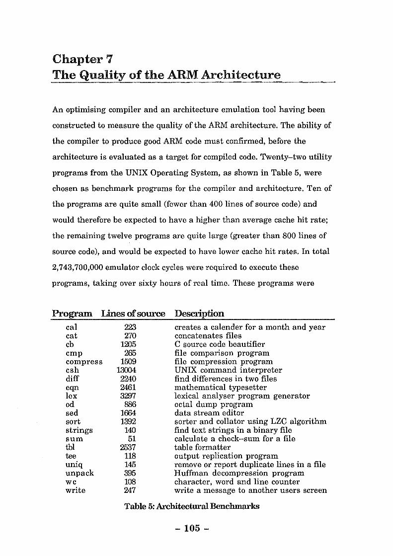
Chapter 7 The Quality of the ARM Architecture
An optimising compiler and an architecture emulation tool having been
constructed to measure the quality of the ARM architecture. The ability of
the compiler to produce good ARM code must confirmed, before the
architecture is evaluated as a target for compiled code. Twenty-two utility
programs from the UNIX Operating System, as shown in Table 5, were
chosen as benchmark programs for the compiler and architecture. Ten of
the programs are quite small (fewer than 400 lines of source code) and
would therefore be expected to have a higher than average cache hit rate;
the remaining twelve programs are quite large (greater than 800 lines of
source code), and would be expected to have lower cache hit rates. In total
2,743,700,000 emulator clock cycles were required to execute these
programs, taking over sixty hours of real time. These programs were
Program Lines of source Description cal cat cb cmp compress csh diff eqn lex od sed sort strings sum tbl tee un1q unpack we write
223 270
1205 265
1509 13004 2240 2461 3297
886 1664 1392
140 51
2537 118 145 395 108 247
creates a calender for a month and year concatenates files C source code beautifier file comparison program file compression program UNIX command interpreter find differences in two files mathematical typesetter lexical analyser program generator octal dump program data stream editor sorter and collator using LZC algorithm find text strings in a binary file calculate a check-sum for a file table formatter output replication program remove or report duplicate lines in a file Huffman decompression program character, word and line counter write a message to another users screen
Table 5: Architectural Benchmarks
- 105-

chosen to give a mix of C operations, such as character, integer, string,
array and record manipulation, control structures, and procedure
calling, characteristic of real world programs. The large programs are
also used to ensure that the cache effectiveness is properly measured,
small programs tend to stay in the cache indefinitely, causing biased
results. Synthetic benchmarks have not been used for three reasons -
i) they do not test the cache miss rate because they are too small.
ii) they are not necessarily representative of real world programs,
despite the claims made by their authors. If representative
benchmarks can be found it is difficult to balance their execution
times so results are not biased towards programs which represent an
insignificant proportion of real world programs.
iii) there are not enough to form a large suite for an architectural
evaluation.
The C programs here should be representative of real world code, because
they are all real world programs. Admittedly some of the programs are
not commonly used (such as "eqn", "sum", "tbl" and "unpack") but an
architecture should be a good target for all code, not just the most common
code, so their inclusion is justified.
Compiler Performance
Initial tests were done to establish the effectiveness of the ACK compiler
compared to the Acorn compiler, by emulating the code produced by both
the ACK compiler and the Acorn compiler (version 3.31). It was hoped the
ACK compiler would produce significantly better (faster) code, due to the
powerful optimisers that have been used. Figure 9 compares the code
produced by ACK compiler to the code produced by the Acorn compiler for
- 106-
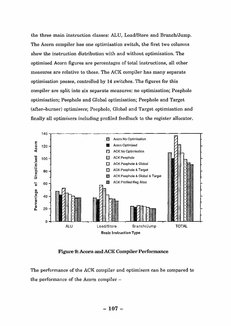
the three main instruction classes: ALU, Load/Store and Branch/Jump.
The Acorn compiler has one optimisation switch, the first two columns
show the instruction distribution with and without optimisation. The
optimised Acorn figures are percentages of total instructions, all other
measures are relative to these. The ACK compiler has many separate
optimisation passes, controlled by 14 switches. The figures for this
compiler are split into six separate measures: no optimisation; Peephole
optimisation; Peephole and Global optimisation; Peephole and Target
(after-burner) optimisers; Peephole, Global and Target optimisation and
finally all optimisers including profiled feedback to the register allocator.
140
~ Acorn No Optimisation 1: ... 0 120 (.)
Ill Acorn Optimised
<C EJ ACK No Optimisation
"0 100 Q) E3 ACK Peephole
.!!.! E D ACK Peephole & Global
-Q. 80 0 El ACK Peephole & Target
1: ::,:) ~ ACK Peephole & Global & Target
- 60 0 m ACK Profiled Reg Alloc
Q) Cl co 40 .... 1: Q) (.) ... Q)
20 c.
0 ALU Load/Store Branch/Jump TOTAL
Basic Instruction Type
Figure 9: Acorn and ACK Compiler Performance
The performance of the ACK compiler and optimisers can be compared to
the performance of the Acorn compiler -
- 107-

i) with no optimisation, the code produced is 36% slower than the
optimised Acorn code.
ii) the peephole optimiser improves the performance by a further 12%
(making the code 22% slower than the optimised code produced by the
Acorn compiler)
iii) the global optimiser increases the performance by a further 13% over
the peephole optimiser, making the code 8% slower than the
optimised Acorn code. This speed improvement is largely due to the
register allocation stage of the optimiser (the load/store column has
the largest reduction).
iv) the target (after-burner) optimiser and the peephole optimiser
improve the performance of the un-optimised ACK code by 38%,
making the code 1% faster than the optimised Acorn code. The
peephole and target optimiser are used by default, as they are very
fast and have little impact on the compile time performance of the
compiler.
v) with the peephole, target and global optimisers engaged, the code
produced is 46% faster than the un-optimised ACK code and 7%
faster than the optimised Acorn code.
vi) profiled register allocation increases the performance by a further
3.5%, resulting in the ACK compiler with all optimisations engaged
producing code over 10% faster than the code produced by the Acorn
compiler with full optimisation.
The major performance loss of the un-optimised ACK code is the 17%
caused by the lack of register allocation. When combined, the peephole
and target optimisers produce code very similar to the optimised Acorn
code, in both instructions generated and execution time. The compile time
of the ACK kit (with the peephole and target optimisers engaged) is better
- 108-

than the Acorn compiler with optimisation, but worse than the Acorn
compiler without optimisation (both compilers were compared on an
Acorn Unix Workstation).
Architecture Performance
The effectiveness of the ARM architecture as a compiler target was judged
by measuring the usefulness of the architectural features. Compiling the
programs listed above, and executing each one with the emulator to
record feature utilisation has provided all the results required. The
utilisation of many of ARM's features have been investigated and these
can be grouped into four sections -
i) Instruction Usage.
The usage of every instruction has been recorded, and the frequency
of many pairs of instructions, to uncover evidence of wasted or
missing instructions. Data Processing instructions which only
reference two registers (because they replace one operand with the
result), Data Processing instructions which avoid explicit compare
instructions by setting the condition flags, the distribution of
immediate (constant) values and instructions which use the barrel
shifter to replace explicit shift instructions were all measured and
the results interpreted.
ii) Branch and Conditional Instructions.
The number of instructions conditionally executed was recorded,
including the number of instructions in loops and the number of
instructions in subroutines. The usefulness of a single cycle compare
and branch instruction was also investigated.
-109-

iii) Memory Accessing Instructions.
The usefulness of the ARM addressing modes was recorded,
including the ability of the register allocator to avoid memory
references by holding frequently used values in registers. The
effectiveness of the multiple load and store instructions was also
measured, including the total proportion of memory references for
which they are responsible.
iv) Cache Performance.
The performance of the standard ARM3 cache was recorded, and the
effectiveness of modifying the cache in several ways was studied.
All measurements were made on the code produced by the ACK compiler,
with all optimisation stages engaged, and profiled feedback to the register
allocator enabled. Measurement of feature usefulness was made by
comparing the speed of execution (using the emulator) of programs both
utilising and not utilising each feature. All results are based on the raw
data reported by the emulator, and thus are exact for the C programs
tested, underlining the importance of the sample C programs chosen to
represent real world applications, so that the results presented here will
reflect the performance of the ARM architecture when executing real
world applications. The cache was only enabled for the measurements of
its performance, all other measurements are for a standard ARM2
Instruction Usage
The instructions executed have been grouped into several similar
sections: ALU arithmetic (such as add and subtract), move, compare
- 110-
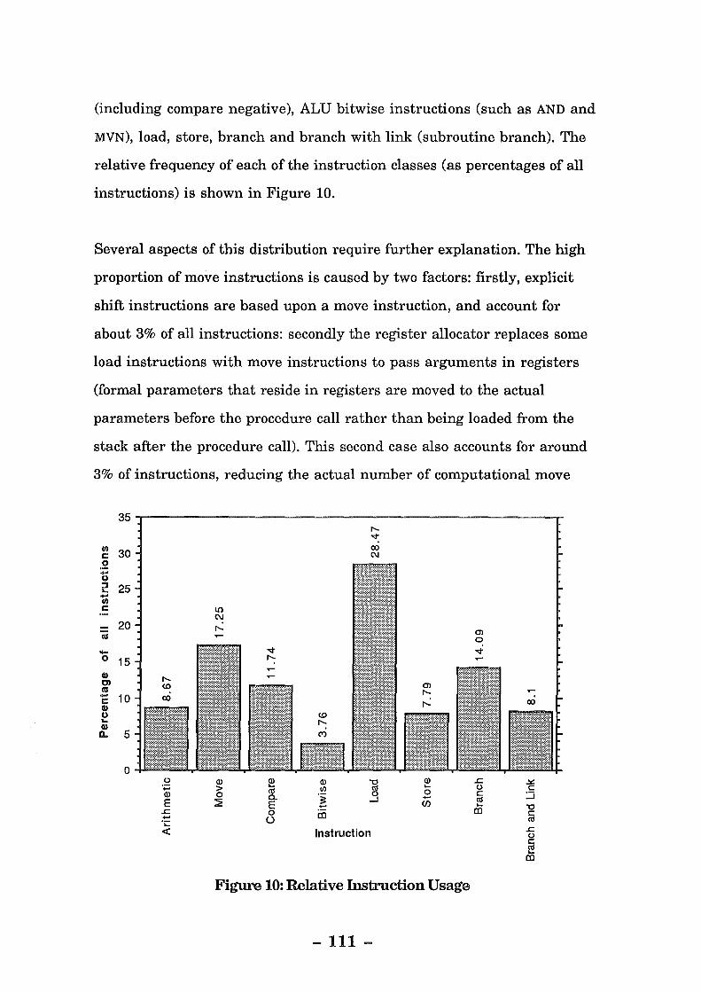
(including compare negative), ALU bitwise instructions (such as AND and
MVN), load, store, branch and branch with link (subroutine branch). The
relative frequency of each of the instruction classes (as percentages of all
instructions) is shown in Figure 10.
Several aspects of this distribution require further explanation. The high
proportion of move instructions is caused by two factors: firstly, explicit
shift instructions are based upon a move instruction, and account for
about 3% of all instructions: secondly the register allocator replaces some
load instructions with move instructions to pass arguments in registers
(formal parameters that reside in registers are moved to the actual
parameters before the procedure call rather than being loaded from the
stack after the procedure call). This second case also accounts for around
3% of instructions, reducing the actual number of computational move
35
II) 30 c:
0 -(,) :::J 25 ... .... II) c:
20 I1S -0 15 G) C) I1S - 10 c: G) (,) ... G)
c.. 5
0 (.)
·.;::; Q)
E ..c: -·;::
Q) ~ Q) -g Q) ..c: ~ > II) .... (.) c: 0
(lj
·~ 0 0 c: :::i
~ a. _J - (lj E - (/) .... '0 0 iii OJ c: () (lj
<( Instruction ..c: (.) c: (lj ....
OJ
Figure 10: Relative Instruction Usage
- 111-

instructions to around 11%. The load word frequency is rather high, and
about 5% of loads and 18% of stores are caused by register spilling in the
register allocator. The twelve available registers are usually enough to
hold all live variables and temporary values, but in about 3% of occasions
three more registers could be effectively utilised by the register allocator
(3% of all instructions were used to spill and reload registers over short
instruction sequences), and as many as eight more could sometimes be
utilised to hold values.
The bitwise operators seem of little use inC code, but the figure is rather
misleading. The programs "sum", "unpack", "od" and "compress" are
responsible for almost all bitwise operations in the twenty-two programs
(bit operations account for about 8% of the instructions in these
programs), so their inclusion in the instruction set is necessary.
Furthermore these instructions may be more prominent in programming
languages like Pascal where they would be used for operations on sets and
arrays of boolean values.
A complete breakdown of the data processing instruction usage is shown
in Figure 11 (as percentages of all instructions). Again the move column
includes around 3% of instructions which are explicit shift instructions,
and another 3% which are part of the procedure calling sequence, and the
proportion of bitwise instructions is low over all programs, but rather
high in some programs. Several instructions are not used by the compiler:
Add with Carry, Subtract with Carry and Reverse Subtract with Carry are
not used by Cas language does not deal with integers greater than 32 bits.
In languages like Lisp with arbitrary precision integers these
instructions would be useful. Setting the condition codes from the result of
- 112-
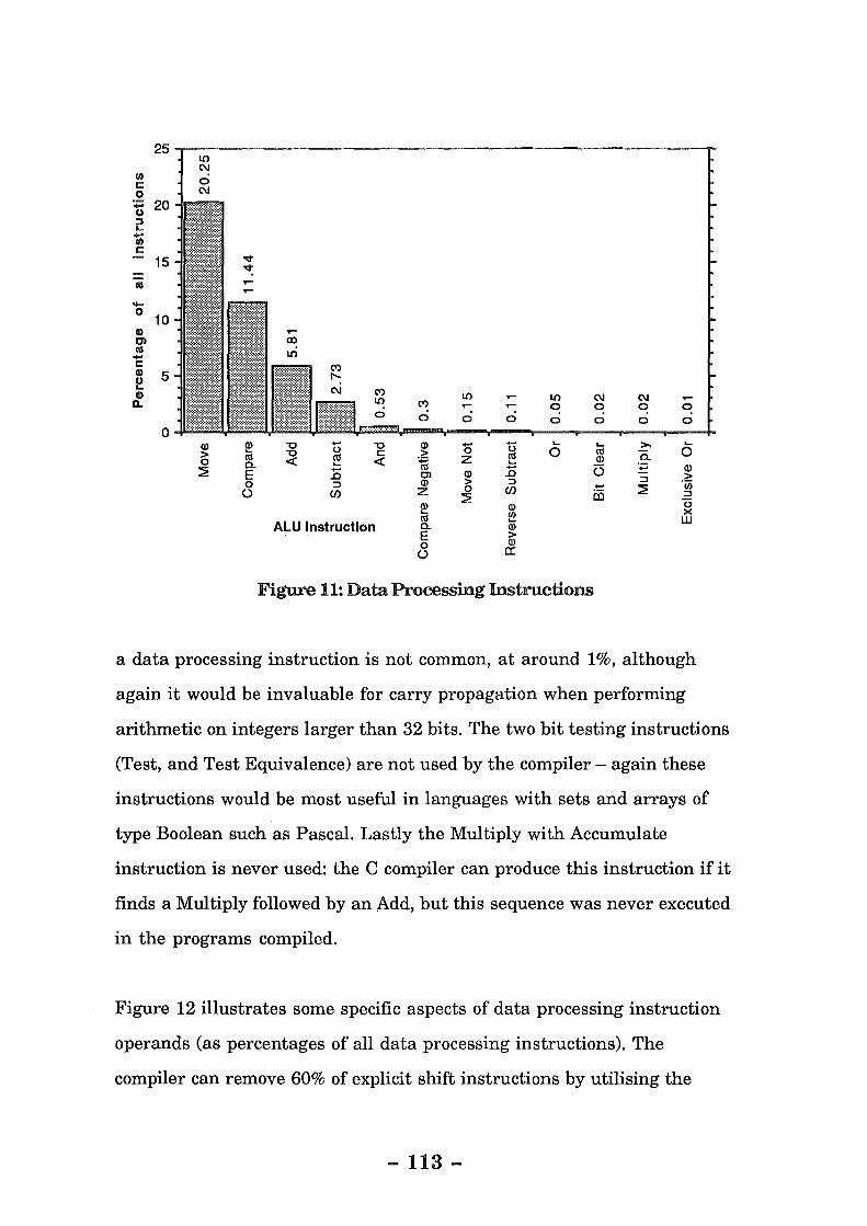
C\1 .,.... 0 0
0 0
>. ..... a. 0
·.;:::; Q)
::I .~ ::2: (/)
::I C3 >< lU
Figure 11: Data Processing Instructions
a data processing instruction is not common, at around 1%, although
again it would be invaluable for carry propagation when performing
arithmetic on integers larger than 32 bits. The two bit testing instructions
(Test, and Test Equivalence) are not used by the compiler- again these
instructions would be most useful in languages with sets and arrays of
type Boolean such as Pascal. Lastly the Multiply with Accumulate
instruction is never used: the C compiler can produce this instruction if it
finds a Multiply followed by an Add, but this sequence was never executed
in the programs compiled.
Figure 12 illustrates some specific aspects of data processing instruction
operands (as percentages of all data processing instructions). The
compiler can remove 60% of explicit shift instructions by utilising the
- 113-

Ill c 60 0 -u ::J ...
50 -Ill c
m 40 c ·u; Ill Cl) u 30 0 ... D.
as 20 .... as c -0 10 Cl)
"<t
m as 0 .... 0 c Cl) Q) ..... E 0> E 0> Ill u n; Q) Q) Q) Ill .l!:l ... - E ..... E ..... "'0 Cl) .!!! c:: I'd D.
"'0 0> ~ >. ~ :0 Q) >. >.
E Q) .0 Q) Q)
a: .0 .0 0.. E E .:::: ~ .:::: :c :E 0 .§ :c ..c::. 0 (/) ..c::. (/) (/) (/) ~ Q)
Operand Type - :t= - 0> . !::! - :§ ..... :§ :§ I'd 0.. 0.. _J
0.. X 0.. E X LU E LU
Figure 12: Data Processing Operands
barrel shifter to modify the second operand of data processing
instructions. Most of these shifts were applied to add and reverse subtract
instructions, because it is these instructions (along with move) that are
used to evaluate multiplications by constant values (and to calculate
addresses for elements in two dimensional arrays). Of the remaining 40%
(combined with move instructions), about half were used for constant
multiplications, and the rest are unavoidable because of code sequences
(in C) such as
a = a<< 1 ; /* left shift 'a' by 1 bit */
inside a loop, which force the register containing "a" to be explicitly
shifted, or are used to sign-extend bytes or halfwords. On average the
barrel shifter increases the execution speed of programs by 2.5%, with a
maximum of 14% for the program "sum".
- 114-

Figure 12 also indicates that a two operand instruction format (where the
value in one operand register would be replaced with the result value)
would only be used in 12.79% of data processing instructions, and the
more general three operand format is therefore useful in over 87% of Data
Processing instructions and completely justified.
The percentage of immediate values which could not be encoded as part of
a data processing instruction (using the eight bit, rotated operand format)
is also shown in Figure 12. The low figure of 0.14% is due to the compiler
allocating a register to hold constants that cannot be encoded as an
immediate operand, thus lowering their dynamic frequency.
Figure 13 shows the distribution of immediate operands values used in
data processing instructions (as percentages of all data processing
immediate operands). The value for negative one is caused by the compiler
using the compare negative instruction (with one as the operand) and the
move not instruction (with zero as the operand). Altering the immediate
field to hold a simple twelve bit constant would degrade the performance of
C code by 2%, mainly because the current rotated immedi~te operands are
useful for loading the addresses of global variables and data structures.
Branch and Conditional Instruction Utilisation
Figure 14 shows the distribution of conditional non Branch instructions
(as percentages of all instructions). Nearly 11% of instructions were
conditional, and the condition failed in 58% of these instructions. The
average number of conditional instruction in sequence is 1.4. If
conditional instructions are not utilised, the code size increases by 8%
- 115-
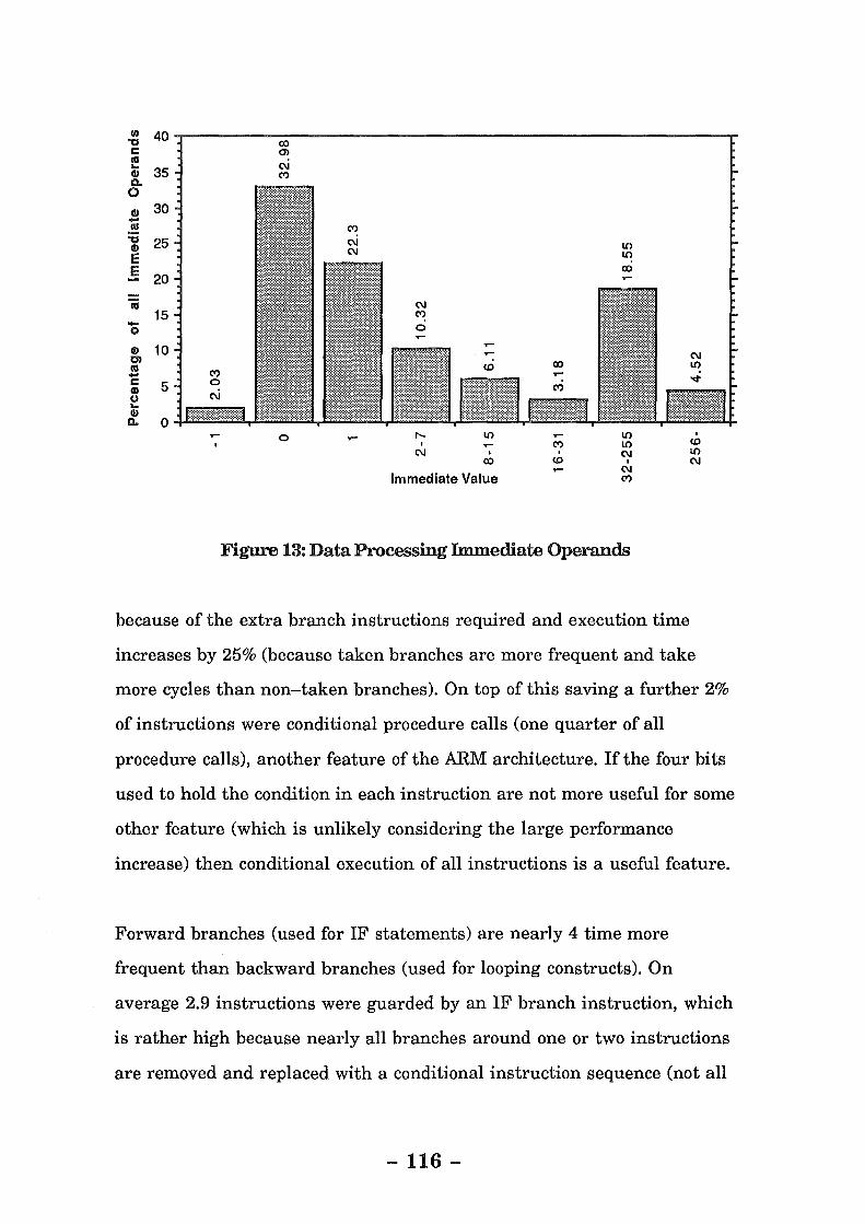
Ill 40 "C CX) c Ol CCI
C\1 ... 35 (I) ('I)
D. 0 (I) 30 -.!
"C 25 (I)
E E 20
iii 15 -0
(I) 10 C) CCI ('I) -c 5 0 (I) () C\1 ... (I)
D. 0 .-
I I
C\1 I I
CX) (0 I
C\1 Immediate Value ('I)
Figure 13: Data Processing Immediate Operands
because of the extra branch instructions required and execution time
increases by 25% (because taken branches are more frequent and take
more cycles than non-taken branches). On top of this saving a further 2%
of instructions were conditional procedure calls (one quarter of all
procedure calls), another feature of the ARM architecture. If the four bits
used to hold the condition in each instruction are not more useful for some
other feature (which is unlikely considering the large performance
increase) then conditional execution of all instructions is a useful feature.
Forward branches (used for IF statements) are nearly 4 time more
frequent than backward branches (used for looping constructs). On
average 2.9 instructions were guarded by an IF branch instruction, which
is rather high because nearly all branches around one or two instructions
are removed and replaced with a conditional instruction sequence (not all
- 116-

14 Ill 13 c 0 12 .... () 11 :I ...
10 -Ill c 9 8
Ill 7 - 6 0
Gl 5 m 4 Ill -c 3 Gl O'l CX) () 2 ... <0 <0 ,.._ Gl 0 0
.,.... c. 1 0
0 -' (ij (ij c (ij (ij c ~ ~ :::J :::J (lj :::J :::J (lj
tlf c- ..c c- c- ..c c
~ UJ 1- UJ UJ - m (/) "iii - ..... ..... .... (/) c 0 Q) 0 z - 0 Q) => (lj (/) -'
Q) (/) .... Condition Type
..... Q) Q)
(!) -' Ia Q) .....
(!)
Figure 14: Conditional Non-Branch Instructions
short branches are removed because some are required in complex
boolean expressions to branch around a second compare and branch).
On average just thirty two instructions were executed between procedure
calls, underlining the need for efficient procedure entry and exit
mechanisms.
Almost all conditional branch instructions branch around fewer than one
thousand instructions, and the proportion of conditional branch
instructions that are preceded by compare instructions is over 95%. If a
single cycle compare and branch instruction can be implemented a 10%
performance increase could be made due to the vast reduction in the
number of compare instructions used before branches. The feasibility of
such an instruction is discussed later.
- 117-

Nearly 70% of subroutine branches were made to Operating System
libraries, underlining the importance of register allocation at link time.
Modern UNIX systems are tending towards shared Operating System
libraries, where many processes share the same library code, so this code
dictates the register usage in programs which call these libraries.
Memory Accessing Instructions
The frequency of different addressing modes is shown in Figure 15, (as
percentages of all memory accessing instructions) including the
frequency of the load and store multiple register instructions. The scaled
index and auto increment and auto decrement addressing modes are well
utilised by the compiler, and together provide a 7% performance increase
by saving shift instructions and addition/subtraction instructions (or
both). The twelve bit immediate offset field caters for all immediate offsets,
an eight bit rotated immediate operand (as in the Data Processing
instructions) would not be beneficial. Load instructions are responsible for
73% of single register memory access instructions, stores are the
remaining 27%. This distribution is the same across all addressing
modes.
On average 6.3 registers are saved by each multiple transfer instruction,
making them responsible for over fifty percent of the total memory traffic.
Most of these instructions (97%) use the decrement-before (DB)
addressing mode to access the procedure call stack, the rest replace
sequential single register memory accesses. Fifty-three percent of
multiple register memory accesses were loads. These instructions are
responsible for a 34% performance increase.
- 118-
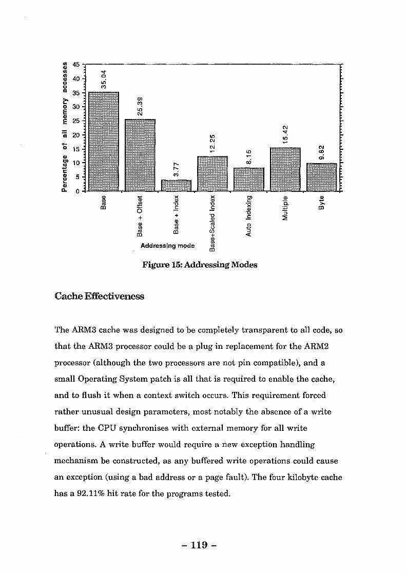
Ill 45 G) Ill Ill 40 G) (,) (,) m 35 :::... .... 0 30 E G)
E 25
m 20 -0 15 G)
C'l 10 m .... c: G) 5 (,) ... G)
D. 0
! - X X C) Q) Q) Q) Q) Q) c: "C.. -$ -o -o ·x >.
OJ .... E E ·.;::::; OJ 0 Q)
-o ::J
+ + -o E ~ Q)
Q) Q) Iii l{l 0
l{l 0 -OJ (/) ::J OJ + <C
Q)
Addressing m9de (/) ro
OJ
Figure 15: Addressing Modes
Cache Effectiveness
The ARM3 cache was designed to be completely transparent to all code, so
that the ARM3 processor could be a plug in replacement for the ARM2
processor (although the two processors are not pin compatible), and a
small Operating System patch is all that is required to enable the cache,
and to flush it when a context switch occurs. This requirement forced
rather unusual design parameters, most notably the absence of a write
buffer: the CPU synchronises with external memory for all write
operations. A write buffer would require a new exception handling
mechanism be constructed, as any buffered write operations could cause
an exception (using a bad address or a page fault). The four kilobyte cache
has a 92.11% hit rate for the programs tested.
- 119-

hnproving the ARM architecture
Together the unusual architectural features of ARM increase
performance by 73.5% compared to a more traditional RISC architecture
like MIPS. The most significant performance losses are caused by the lack
of delayed loads, the lack of delayed branches and the high proportion of
branch instructions that are preceded by compare instructions.
The ARM2 architecture cannot accommodate delayed loads, because of
the von Neumann memory architecture, which cannot deliver a new
instruction and a data word in the same cycle. Delayed branches were not
added to the architecture due to the complications they would make to
ARM's simple and elegant architecture. By altering the ARM3
architecture (and therefore the emulator, compiler and optimisers) the
effect these changes have on performance has been measured.
The absence of delayed load instructions is a result of the strict von
Neumann memory system, which cannot deliver a new instruction (to
keep the pipeline full) and a word of data (loaded by a load instruction) in
the same cycle, causing a load delay of one cycle. This delay is also
incurred by the store instructions. The complex addressing modes utilise
this wasted cycle to provide a 7% performance increase. The multiple
register transfer instructions ensure consecutive load or store
instructions to consecutive memory addresses only incur one pipeline
delay (rather than one for each word transferred), to provide a 34%
performance increase.
-120-

Altering the ARM3 architecture to accommodate delayed loads is possible,
but requires several changes to the architecture and additions to the
software-
i) adoption of a Harvard memory architecture, with both the address
and data buses connected to separate caches. Both the instruction
and data caches have 512 word entries (2 KiloBytes).
ii) lengthening of the execution time of the auto-indexing addressing
modes to two cycles to allow time for the base register modification.
This type of load would not require a load delay slot as a new
instruction is not required in the second cycle, so the data can be
loaded then.
iii) adding another pass to the assembler to schedule instructions for the
load delay slot, by looking either before the branch for an instruction
which can be shifted into the load delay slot or after the branch (both
if the branch is taken or not taken) for an instruction which does
depend on the result of the branch.
Implementing delayed loads increased performance by 14.8%. The
multiple register transfer instructions are of little use in this modified
architecture, providing less than 1% more performance, and could be
removed. The multiple register transfer instructions are the main reason
that the architecture has just sixteen registers, where thirty-two would be
more useful. Unfortunately to encode 3 five bit register numbers in a data
processing instruction would require the removal of the condition field,
which would imply a 25% performance loss, outweighing the 3%
performance increase the extra registers could be expected to provide.
- 121-

Delayed branches were not included in the ARM design because of the
complexity they add to the exception handling mechanism (two Program
Counters are required to record the CPU state because an exception can
occur in both the branch delay slot and the branch destination at the same
time), and adding a register for the second program counter, and special
instructions to access it is rather messy. There is a simple way to add the
second Program Counter to the ARM3 architecture however, as one of the
cache controller registers (registers 9 to 16 are currently unused). Adding
delayed branches to the architecture increased performance by 12.3%, and
reduced the performance increase of conditional instructions to about 4%
(because the delay slots after branches around one or two instructions are
very easy to fill), which makes their removal in favour of thirty-two
registers much more controversial.
Both the above architecture changes (delayed loads and delayed branches)
make the resulting architecture incompatible with earlier ARM
architecture. A third architectural change improves the performance of
the ARM architecture and maintains full compatibility with the earlier
architectures. Adding a general purpose, single cycle compare and
branch instruction to the ARM architecture would increase performance
by 10.34%, because most (95%) of branch instructions are preceded by a
compare instruction. It is not possible to fit all the information necessary
into 32 bits for an instruction to replace all compare and branch
instructions, but using one of the undefined instruction formats it is
possible to add an instruction with two registers or a register and a four
bit integer, a (second) four bit compare condition field, and an 1024
instruction offset (1024 instructions could be branched both forwards and
backwards). Adding this less general instruction improved performance
9.84%. A problem with this instruction is the extra hardware required for
- 122-
a second subtract unit to calculate the compare result (as the shifter and
the main ALU would be required for the branch target calculation).
It is possible to restrict the type of branch to just equal and not-equal,
which do not require a full carry propagating subtraction unit for the
comparison, and the branch offset can be increased to 8192 instructions.
This option increased performance by 8. 72%, and does require as much
extra hardware, changes to the instruction field extraction unit, to remove
the branch offset and send it directly to the ALU, and to the ALU buses to
support the two calculations at once. The existing register read ports can
be used for the compare, and the existing ALU for the branch calculation.
The assembly mnemonic is also rather strange due to the two condition
fields (one for the entire instruction, the other for the branch), but this
instruction is probably best produced automatically by the assembler
anyway, as only at this stage is the magnitude of a branch offset known to
decide if it can be utilised. This feature was probably not included in the
ARM architecture because it does not follow the RISC discipline, as there
would be two ways to perform some tasks, complicating the architecture.
As the clock rate of the ARM architecture increases, it is likely that the
execution stage of the instruction pipeline will take the longer than either
the instruction fetch or the instruction decode stages. The barrel shifter
lengthens the critical CPU data path by 15%. The execution stage of the
pipeline could be shortened (by 15%) by removing the barrel shifter from
the main data path, and making instructions which utilise the shifter
take an extra cycle (except branch instructions, which need a two bit left
shift for the branch offset, this could be accommodated in one cycle). Shifts
whose magnitude is held in a register (rather than an immediate
constant) already take an extra cycle because three register reads are
- 123-
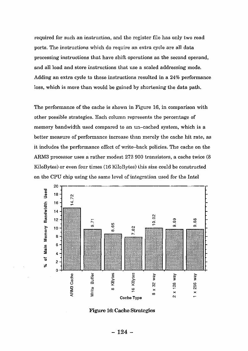
required for such an instruction, and the register file has only two read
ports. The instructions which do require an extra cycle are all data
processing instructions that have shift operations as the second operand,
and all load and store instructions that use a scaled addressing mode.
Adding an extra cycle to these instructions resulted in a 24% performance
loss, which is more than would be gained by shortening the data path.
The performance of the cache is shown in Figure 16, in comparison with
other possible strategies. Each column represents the percentage of
memory bandwidth used compared to an un-cached system, which is a
better measure of performance increase than merely the cache hit rate, as
it includes the performance effect of write-back policies. The cache on the
ARM3 processor uses a rather modest 272 900 transistors, a cache twice (8
KiloBytes) or even four times (16 KiloBytes) this size could be constructed
on the CPU chip using the same level of integration used for the Intel
20 "0 Q)
18 !II :::J
..c .... 16 "0 'i 14 "0 c: CIS 12 m ~ 10 0 E 8 Q)
::iE c: 6
'(Q ::iE 4 -0
2 'fP.
0 Q)
..... IJ) IJ)
~ ~ ~ ..c ~ Q) Q) (.) ...... - - ~ ~ ~ >. >. ro :::J (I) (I) () (I)
~ ~ C\J co (0
C') C') C\J LO
:2: Q) co (0 >< C\J -a: ·.:: >< ><
<( $: co Cache Type C\J
Figure 16: Cache Strategies
-124-

80860 and 80486 processors, and the Motorola 68040 processors (each
utilise 1.2 million transistors). The usefulness of a write buffer is also
investigated. When designing the ARM3, Acorn performed their own
testing on placement strategies, and these have been confirmed here for
caches up to 16 KiloBytes. The first column is the standard ARM3 cache
(Four KiloBytes, write-through, 64 way set associative, virtual mapped,
random replacement). The second column shows the main memory
bandwidth decrease using a write back strategy, with a write buffer (of 8
words). The third and fourth column indicate the bandwidth decrease 8
and 16 Kilobytes of cache will provide (both including write buffers). The
fourth column shows the decrease over the second column (ARM3 cache
with a write buffer) caused by changing to an LRU replacement strategy
(even though this is difficult with large cache sets). The fifth column
indicates the bandwidth used by a cache with eight thirty two way sets, the
the sixth and seventh column shows the bandwidth of two 128 ways sets
and one 256 way set (fully associative). As can be seen a write buffer
provides the most significant decrease, yielding nearly 5%. The exception
handling required for the write-buffer can be stored as part of the cache
control co-processor. A larger cache is clearly a simple method for using
more chip space to lower the main memory bandwidth used.
The actual performance gained achieved by lowering the main memory
bandwidth used by the processor is dependant on the speed of main
memory in comparison to the speed of cache memory, and how long the
processor must wait before it can access the main memory. A typical
main memory speed is 6 MegaHertz (for a random access), and ARM3
processors are currently available with 30 MegaHertz clock speeds, thus a
main memory access takes the equivalent of five processor (cache) cycles.
Another 80% of a main memory cycle will be typically used for
- 125-

synchronization and bus delays (50% waiting for the start of the next
memory cycle, and the memory bus is heavily utilised by the video
circuitry, causing 30% extra delays). Thus nine processor cycles will be
incurred for each main memory access. By multiplying the percentage
reduction in the main memory bandwidth by this nine cycle delay, the
performance benefit of each caching strategy can be judged. The adoption
of a write buffer would yield approximately 40% more performance, and
combined with the larger cache (of 16 KiloBytes) over 60% more
performance can be gained.
The compact encoding of ARM's instruction set increases cache
performance by a large extent. The lack of many branch instructions, the
shift operations that are combined with data processing instructions, the
complex addressing modes, and the multiple memory transfer
instructions that replace several single register transfers all contribute to
a 45% decrease in the instruction memory bandwidth used (and hence
increase the effectiveness of the cache) compared to more typical RISC
architectures, justifying their inclusion in the architecture, even if
delayed branches and/or delayed loads had been implemented. Programs
with a high number of procedure calls benefit more (up to 55%) from the
compact instructions (due to the increase in the proportion of multiple
register transfer instructions used), making this feature more efficient at
lowering the memory bandwidth used by the processor than the SP ARC
architecture's register windows [Morr88].
- 126-

Conclusion
The Amsterdam Compiler Kit has proven to be a useful tool in the
construction of an optimising compiler for the ARM architecture. The
only optimisation the back-end could not generate was for the utilisation
of conditional instructions. The addition of a new register allocator,
incorporating information passed back from run time profiling to
enhance allocation has resulted in a compiler that produces 10% better
(faster) code than the commercial Acorn compiler, and comparable to the
code produced by a good assembly language programmer.
The software emulator has allowed a large number of real world
programs to be executed to quantify the real world performance of the
architecture when executing code produced from a high level language
compiler.
After examining the results of this study it is difficult to find fault with the
ARM2 architecture, it is very well suited to the low cost applications it was
designed for. The elegance of the architecture makes it suitable for the
assembly language programming often used in small embedded control
systems, as well as a good target for the compiled code executed by high
performance computers. The architecture makes full use of available
memory bandwidth, and the page mode access speed of modern DRAM
memory.
Delayed Load instructions have not been implemented in the ARM
architecture because the inexpensive von Neumann memory architecture
cannot deliver two words in one cycle required for a delayed load. The von
Neumann architecture also forces two cycles for Store instructions. The
- 127-
complex addressing modes efficiently use 20% of the second cycle of load
and store instructions, but a load delay slot can be at least 60% utilised.
The multiple register transfer instructions yield a 34% performance
increase by exploiting the paged mode access speed of the memory.
Delayed branch instructions have not been implemented because of the
complexity they add to the ARM architecture. The conditional execution of
instructions removes practically all short branch instructions (those
skipping around one or two instructions), consequently replacing 37% of
all branch instructions. A delayed branch instruction (which can be
added to the ARM3 architecture) would increase performance by 12%.
A single cycle compare and branch instruction would yield 8.7% more
performance, but its rather specific use tends to disobey the RISC
philosophy of one fast way to do each task.
The barrel shifter is justified as part of the main execution data path - the
number of explicit shift instructions it removes yields better performance
(24%) than the lengthening of the clock cycle it causes (15%) when the
processor is performance bound by the rate at which it can execute
instructions (which would occur if the instruction fetch and decode times
were to decrease at high clock rates).
The number of instructions required to execute a given task is reduced by
45% because of the compact encoding of ARM instructions. Although
these instructions take longer to decode, an ARM2 implementation will
always be limited by the memory access time, so the decrease in required
memory bandwidth is much more significant. This feature alone
- 128-

outstrips the memory bandwidth that could be save by using register
windows (as in the SPARC architecture).
The ARM3 architecture maintains full user code compatibility with
ARM2 (Operating System code must be patch to enable the cache, and
perform cache flushing when a processor context switch occurs). This
compatibility causes a performance loss, mainly due to the lack of a cache
write buffer- all store instructions cause the processor to slow to the
speed of the main memory while the data is written to memory. On a
typical implementation with a cache memory five times faster than the
random access speed of the main memory, a write buffer increases
performance by 40%, and combined with a 16 KiloByte cache a
performance increase of 60% can be achieved.
The commercial computer market illustrates that ARM based machines
can achieve better price/performance ratios than other computers due the
low cost of the processor and memory required to gain good performance.
Other computers suffer from the need for dedicated logic to lower the
workload on their complex processors, and require large, expensive
caches to match ARM's versatility and low memory requirements. ARM's
simple elegance allows it to be produced very inexpensively, and its low
memory bandwidth makes a future ARM based multi-processor an
attractive possibility.
- 129-

Acknowledgements
I wish to thank many people who have helped me with this research. Dr
Michael Maclean supervised the work and proof read many drafts of the
text. Dr Bruce McKenzie for his many helpful comments on compiler
design and the philosophy of the Amsterdam Compiler Kit.
The staff and graduates of the Computer Science department at
Canterbury, who have provided much support, both intellectually and
otherwise. Mr Kevin Rodgers, for his foresight in purchasing an ARM
based computer for Shirley Boys' High School (keeping his head while
others were losing theirs). Dr Pi]:) Forer and the staff of the Geography
department at Canterbury for allowing me unlimited access to their lab of
Acorn computers. To Acorn Computer (UK) Ltd, for answering many
queries, and for designing and supporting the ARM processor.
Mr Graham Stairmand for his dedicated proof reading, many helpful tips
and a great deal of encouragement.
Financial support was supplied by a Battersby Scholarship in 1989 from
Datacom Ltd.
Finally to my girlfriend, Angela, for her encouragement over the past four
years, and to my mother her support during my six years of tertiary
education, and to my father, for making me be both theoretical and
practical.
- 130-

Bibliography
[Aho86] Aho, A.V. Sethi, R. and Ullman, J.D. Compilers Principles,
Techniques and Tools. Addison Wesley, Reading,
Massachusetts, 796p
[AMD87] Advanced Micro Devices Am29000 Streamlined Instruction
Processor Users Manual. Advanced Micro Devices Inc. 901
Thompson Place, PO Box 3453, Sunnyvale, CA 94088
[Ausl82] Auslander, M.A. and Hopkins, M. An Overview of the PL.B
compiler. Proceedings of the SIGPLAN '82 Symposium on
Compiler Construction SIGPLAN Notices 17(6) June 1982
[Bal85] Bal, H.E. The design and implementation of the EM Global
Optimiser. Rapport IR-99 Vrije Universiteit Amsterdam
March 1985
[Bal86] Bal, H. and Tanenbaum, A.S. Language- and Machine
Independent Global Optimisation on Intermediate Code.
Computer Languages 11(2) pp105-1211986
[Bern89] Bernstein, D., Goldin, D.Q., Golumbic, M.C., Krawczyk, H.,
Mansour, Y., Nahshon, I. and Pinter, R.Y. Spill code
minimisation techniques for optimising compilers. SIGPLAN
Notices 24(7) July 1989
[Brig89] Briggs. P., Cooper. K.D., Kennedy. K. and Torczon. L.
Coloring Heuristics for Register Allocation. SIGPLAN
Notices 24(7) pp275-284 1989.
[Cate88] Cates. R. Processor Architecture Considerations for
Embedded Controller Applications. IEEE Micro 8(3) pp28-37
June 1988
- 131-

[Chat81] Chatin, G.J., Auslander, M.A. Chandra, A.K. Cocke, J.
[Chat82]
Hopkins, M.E. and Markstein, P.W. Register Allocation Via
Graph Colouring. Computer Languages 6 pp47-57 1981
Chatin, G.J. Register Allocation and Spilling via Graph
Colouring. Proceedings of the SIGPLAN '82 Symposium on
Compiler Construction SIGPLAN Notices 17(6) June 1982
[Chow84] Chow, F. and Hennessey, J. Register Allocation by Priority
based Coloring. Proceedings of the SIGPLAN '84 Symposium
on Compiler Construction SIGPLAN Notices 19(6) June 1984
[Chow88] Chow, F.C. Minimizing Register Usage Penalty at Procedure
Calls. Proceeding of the SIGPLAN '88 Conference on
Programming Language Design and Implementation June
22-24 1988 pp 85-94
[Ditz87] Ditzel, D.R., McLellan, H.R. and Berenbaum, A.D. The
Hardware Architecture of the CRISP Microprocessor.
Proceedings of the 14th Annual Symposium on Computer
Architecture, pp309-319
[Dobb88] Dobbs, C., Reed, P. and Ng, T. Supercomputing on Chip:
Genesis of the 88000. VLSI Systems Design May 1988 pp24-33
[Furb89] Furber, S.B. VLSI RISC Architecture and Implementation.
Marcel Dekker New York, 365p.
[Gros88] Gross, T.R., Hennessy, J.L., Przybylski, S.A. and Rowen, C.
[Heid90]
Measurement and Evaluation of the MIPS Architecture and
Processor. ACM Transactions on Computer Systems, 6(3)
pp229-257,August1988
Reid. J. Mac World Magazine 7(5), MacWorld
Communications, 501 Second Street, San Franciso pp280-289,
Mayl990
- 132-

[Henn82] Hennessy, J.L., Jouppi, N., Przybylski, S.A., Rowen, C.,
Gross, T.R., Baskett, F. and Gill, J. MIPS: A Microprocessor
Architecture. IEEE Micro Special Report pp17-22 1982
[Henn84] Hennessey, J.L. VLSI Processor Architecture. IEEE
Transactions on Computer 33(12) pp1221-1246
[IBM90] IBM Australia Ltd. The RISC System I 6000 Range. Customer
Information Issue 46 February 1990
[Jagg90] Jaggar, D.V. Fast Ziv-Lempel Decoding on a RISC.
Submitted for Publication with IEEE Transactions on
Computers.
[Jone88] Jones, D. The MC88100 RISC processor. Electronic
Engineering May 1988 pp45-55
[Jone89] Jones, D. MC88100 RISC. Electronic and Wireless World
94(1929) pp637-642 July 1988
[Kane88] Kane, G. MIPS RISC Architecture. Prentice Hall. Englewood
Cliffs N .J, 288p
[Kern78] Kernighan, B.W. and Ritchie, D.M. The C Programming
Language. Prentice Hall Englewood Cliffs NJ, 227p
[Lehr89] Lehrer, M.A. Second Generation RISC Processor. Electronic
and Wireless World 94(1929) pp689-691 July 1988
[McKe87] McKerrow, P. Performance Measurement of Computer
Systems. Addison Wesley, Reading, Massachusetts, pp65-97
[McKe89] McKenzie, B.J. Fast Peephole Optimisation Techniques.
Software Practice and Experience 19(2) pp1151-1162,
December 1989
[Mele89] Melear, C. The Design of the 88000 RISC Family. IEEE Micro
9(2) pp26-38 1989
[MIPS88] MIPS Computer Ssystems Inc. Language Programmer's
Guide. pp4.1-4.37 MIPS Computer Systems Inc.
- 133-

[Morr88] Morrison, N. Register Windows us. General Registers: A
Comparison of Memory Access Patterns. Technical Report,
University of California, Berkeley, California.
[Moto85] Motorola Inc. MC68020 32 Bit Microprocessor User's Manual.
Prentice Hall, Englewood Cliffs. NJ, 438p
[Patt80] Patterson, D.A. and Ditzel, D.R. The Case for the Reduced
Instruction Set Computer. Computer Architecture News 8(6)
pp25-33
[Patt81] Patterson, D.A. and Sequin, C. RISC I: A Reduced
Instruction Set VLSI Computer. Proceeding of the 8th Annual
Symposium on Computer Architecture, ACM SIGARCH
Computer Architecture News 9(3) pp443-457 (1981)
[Patt82] Patterson, D.A. and Sequin, C. A VLSI RISC. IEEE Computer
15(9) ppB-18 September 1982
[Patt85] Patterson, D. Reduced Instruction Set Computers.
Communications of the ACM 28(1) pp 8-211985
[Radi82] Radin, G. The 801 Minicomputer. SIGPLAN Notices 17(4) 1982
[Rowe88] Rowen, C., Johnson, M. and Ries, P. The MIPS R3010
Floating-Point Coprocessor. IEEE Micro June 1988 pp53-62
[Smit82] Smith, A.J. Cache Memories. ACM Computing Surveys 14(3)
pp 4 73--530 1987
[SPEC90] Standard Performance Evaluation Co-Operative Newsletter,
2(1) 1990 25p
[Sun87a] Sun Microsystems Inc. A RISC tutorial. Sun Technical
Report, 15p
[Sun87b] Sun Microsystems Inc. The SPARC™ Architecture Manual,
Version 7 Revision A, October 22, 1987
- 134-

[Tami83] Tamir, Y. and Sequin, C. Strategies for Managing the
Register File in RISC. IEEE Transactions on Computers
32(11) pp977-989 1983
[Tane78] Tanenbaum. A.S. Implications of Structured Programming
for Machine Architecture. Communications of the ACM, 21(3)
pp237 -246 1978
[Tane83a] Tanenbaum, A.S., van Staveren, E.G., Keizer, E.G. and
Stevenson, J.W. A Practical Toolkit for making Portable
Compilers. Communications of the ACM 26(9) pp654-660
September 1983
[Tane83b] Tanenbaum, A.S., van Staveren, E.G., Keizer, E.G. and
Stevenson, J.W. Description of a Machine Architecture for
use with Block Structured Languages. Rapport IR-81 Vrije
Universiteit, Amsterdam August 1983
[VTI89] VLSI Technology Limited. VL86C010 32-Bit RISC MPU and
Peripherals User's Manual. Prentice Hall Englewood Cliffs
NJ 188p.
[Wall86] Wall, D.W. Global Register Allocation at Link Time.
SIGPLAN Notices 21(7) 264-275 1986
[Wall88] Wall, D.W., Register Window us. Register Allocation.
Proceedings of the SIGPLAN '88 pp67-78
[Wils89a] Wilson, R. RISC CPUs tune up for embedded computing.
Computer Design, May 1989 pp 36-38
[Wils89b] Wilson, R. The ARM3 RISC Processor. RISC User
July/August 1989 pp7-9
[Wirt88] Wirth, N. From Modula to Oberon. Software Practice and
Experience 18(7) pp661-670 1988
[Wirt89] Wirth, N. and Gutknecht, J. The Oberon System. Software
Practice and Experience 19(9) pp857-893 1989
- 135-

Appendix A ARM 3 Instruction Set Format
Data Processing
Operand is a shifted register 31 28 Z7 ~ 25 2A 21 20 19 16 15 1211 0
I Cond I 00 II I Opcode lSI Rm Rd I Operand
I = 0 : Operand is a shifted register Shift amount is an immediate 11 76 543 0
Shift amount is in a register
Sh : Type of shift 00 01 10 11
ROR with Shamt 0
LSL LSR ASR ROR RRX
I Shamt I Sh I 0 I Rn I Shamt: Register holding shift amount
11 876 543 0
I Shamt I 0 I Sh Ill Rn I Shamt : Register holding shift amount
Logical Shift Left Logical Shift Right Arithmetic Shift Right Rotate Right Rotate Right with Extend
I = 1 : Shift amount is an immediate 11 8 7 0
I Shamt I Immediate I Cond: Condition Code OpCode : Operation Code
0000 EQ Equal 0000 AND 0001 NE Not Equal 0001 EOR 0010 cs Carry Set 0010 SUB 0011 cc Carry Clear 0011 RSB 0100 MI Minus 0100 ADD 0101 PL Plus 0101 ADC 0110 vs Overflow Set 0110 SBC 0111 vc Overflow Clear 0111 RSC 1000 HI Higher 1000 TST 1001 LS Lower or Same 1001 TEQ 1010 GE Greater than or Equal 1010 CMP 1011 LT Less Than 1011 CMN 1100 GT Greater Than 1100 ORR 1101 LE Less than or Equal 1101 MOV 1110 AL Always 1110 BIC 1111 NV Never 1111 MVN
S : Set condtion flags Rm : Left hand side operand register number Rd : Destination register number
- 136-
Logical AND Exclusive OR Subtract Reverse Subtract Addition Addition with Carry Subtract with Carry Reverse Subtract with Carry Test Test Equality Compare Compare Negative Logical OR Move Bit Clear Move Negative

Multiply
31 28 'Z7 22 212019 16 15 12 11 8 7 4 3 0
I Cond I 000000 IAISI Rd I Ra I Rn I 1001 I Rm I A :Multiply with Accumulate
Branch
31 28 'Z7 25 24 23
I Cond I 101 ILl PC Offset
L: Branch with link
Single Data Transfer
M 28'Z7~25242322ID2019 ffi15 12ll
I Cond I 0111 IPfUIBI\VILI Rm Rd I
P : Pre I Post indexing Post=O , Pre=l U: Up I Down bit Down=O, Up=l B :Byte I Word bit Word=O, Byte=l W : Writeback flag L :Load I Store bit Store=O, Load=l
Swap Data
M 28'Z7 2322ID2019 ffi15
I Cond I 00010 IBI 00 I Rm I
Rm : Memory address register Rs : Source regiser Rd : Destination register
Block Data Transfer
M 28'Z7 25242322ID2019 ffi15
I Cond I 100 IPfUISI\VILI Rn I
S : Load processor status flags
- 137-
1211
Rd I
Offset
4 3
00001001
Register List
0
0
0
Rs
0
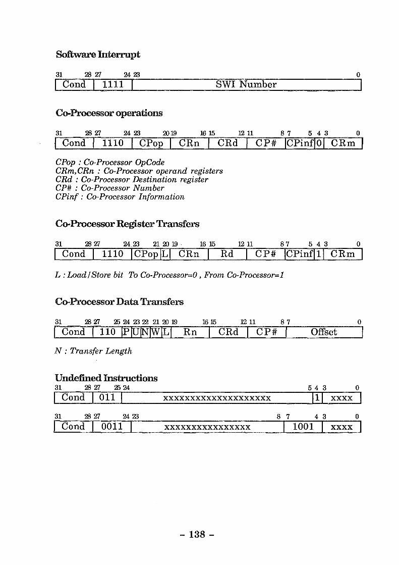
Software lnteiTUpt
31 28 'Z7 24 Z3 0
I Cond I 1111 I SWI Number
Co-Processor operations
31 28 'Z7 24 Z3 2D 19 16 15 12 11 8 7 5 4 3 0
I Cond I 1110 I CPop I CRn I CRd I CP# jCPinfjOj CRm I CPop : Co-Processor OpCode CRm,CRn : Co-Processor operand registers CRd : Co-Processor Destination register CP# : Co-Processor Number CPinf: Co-Processor Information
Co-Processor Register Transfers
31 28 'Z7 24 Z3 21 2D 19 . 16 15 1211 87 543 0
I Cond I 1110 jCPopjLI CRn I Rd I CP# ICPinfjlj CRm I L :Load I Store bit To Co-Processor=O, From Co-Processor=l
Co-Processor Data Transfers
31 28 'Z7 25 24 Z3 22 21 2D 19 1615 1211 87 0
I Cond I 110 IPfUINIWILI Rn I CRd CP# I Offset
N: Transfer Length
Undefined Instructions 31 28 'Z7 25 24 54 3 0
I Cond I 011 I xxxxxxxxxxxxxxxxxxxx 111 xxxx 1
31 28 'Z7 24 Z3 8 7 4 3 0
I Cond 0011 I xxxxxxxxxxxxxxxx I 1001 xxxx I
- 138-

AppendixB EM Instruction Set
Group 1-Load
LOC c Load constant (i.e. push one word onto the stack) LDC d Load double constant (push two words) LOL 1 Load word at 1-th local (1<0) or parameter 0>=0)
LOE g Load external word g LIL 1 Load word pointed to by 1-th local or parameter LOF f Load offsetted. (top of stack+ fyield address) LAL 1 Load address of local or parameter LAE g Load address of external LXL n Load lexical (address of LB n static levels back)
LXA n Load lexical (address of AB n static levels back) LOI s Load indirect s bytes (address is popped from the stack) LOS i Load indirect, i-byte integer on top of stack gives object size LDL 1 Load double local or parameter LDE g Load double external LDF f Load double offsetted (top of stack+ fyield address) LPI p Load procedure identifier
Group 2- Store
STL 1 Store local or parameter
STE g Store external SIL 1 Store into word pointed to by 1-th local or parameter STF f Store offsetted STI s Store indirect s bytes (pop address, then data)
STS . Store indirect, i-byte integer on top of stack gives object size 1
SDL 1 Store double local or parameter SDE g Store double external SDF f Store double offsetted
- 139-

Group 3- Integer Arithmetic
ADI 1 Addition
SBI 1 Subtraction
MLI 1 Multiplication
DVI . Division 1
RMI 1 Remainder
NGI . Negate (two's complement) 1
SLI i Shift left
SRI 1 Shift right
Group 4- Unsigned arithmetic
ADU 1 Addition
SBU i Subtraction
MLU 1 Multiplication
DVU 1 Division
RMU 1 Remainder
SLU 1 Shift left
SRU 1 Shift right
Group 5- Floating point arithmetic
ADF 1 Floating add
SBF 1 Floating subtract
MLF 1 Floating multiply
DVF 1 Floating divide
NGF 1 Floating negate
FIF 1 Floating multiply and split integer and fraction part
FEF 1 Split floating number in exponent and fraction part
Group 6- Pointer arithmetic
ADP f
ADS
SBS 1
Add c to pointer on top of stack
Add i-byte value and pointer
Subtract pointers and push difference as size i integer
- 140-
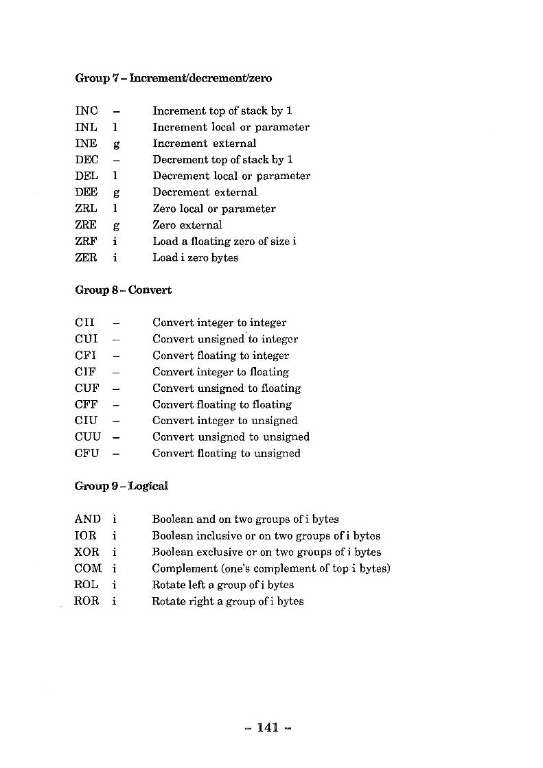
Group 7- Increment/decrement/zero
INC Increment top of stack by 1
INL 1 Increment local or parameter
INE g Increment external
DEC Decrement top of stack by 1
DEL 1 Decrement local or parameter
DEE g Decrement external
ZRL 1 Zero local or parameter
ZRE g Zero external
ZRF 1 Load a floating zero of size i
ZER 1 Load i zero bytes
Group 8- Convert
en Convert integer to integer
CUI Convert unsigned to integer
CFI Convert floating to integer
CIF Convert integer to floating
CUF Convert unsigned to floating CFF Convert floating to floating CIU Convert integer to unsigned cuu Convert unsigned to unsigned
CFU Convert floating to unsigned
Group 9- Logical
AND 1 Boolean and on two groups of i bytes
lOR . Boolean inclusive or on two groups ofi bytes 1
XOR . Boolean exclusive or on two groups of i bytes 1
COM 1 Complement (one's complement of top i bytes)
ROL 1 Rotate left a group of i bytes
ROR 1 Rotate right a group ofi bytes
- 141-
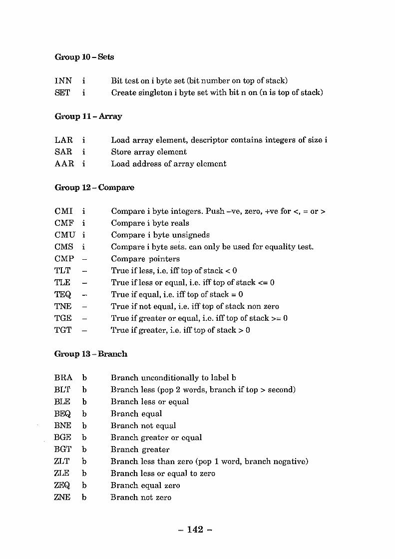
Group 10- Sets
INN 1
SET 1
Bit test on i byte set (bit number on top of stack) Create singleton i byte set with bit n on (n is top of stack)
Group 11-Array
LAR 1
SAR 1
AAR 1
Load array element, descriptor contains integers of size i
Store array element
Load address of array element
Group 12- Compare
CMI CMF
CMU CMS
CMP TLT TLE
TEQ
TNE TGE TGT
1 . 1
1
1
Compare i byte integers. Push -ve, zero, +ve for <, = or > Compare i byte reals
Compare i byte unsigneds Compare i byte sets. can only be used for equality test.
Compare pointers True if less, i.e. iff top of stack < 0 True ifless or equal, i.e. iff top of stack <= 0
True if equal, i.e. iff top of stack = 0
True if not equal, i.e. iff top of stack non zero True if greater or equal, i.e. iff top of stack >= 0
True if greater, i.e. iff top of stack> 0
Group 13- Branch
BRA b Branch unconditionally to label b
BLT b Branch less (pop 2 words, branch if top > second)
BLE b Branch less or equal
BEQ b Branch equal BNE b Branch not equal BGE b Branch greater or equal BGT b Branch greater ZLT b Branch less than zero (pop 1 word, branch negative)
ZLE b Branch less or equal to zero ZEQ b Branch equal zero
ZNE b Branch not zero
- 142-
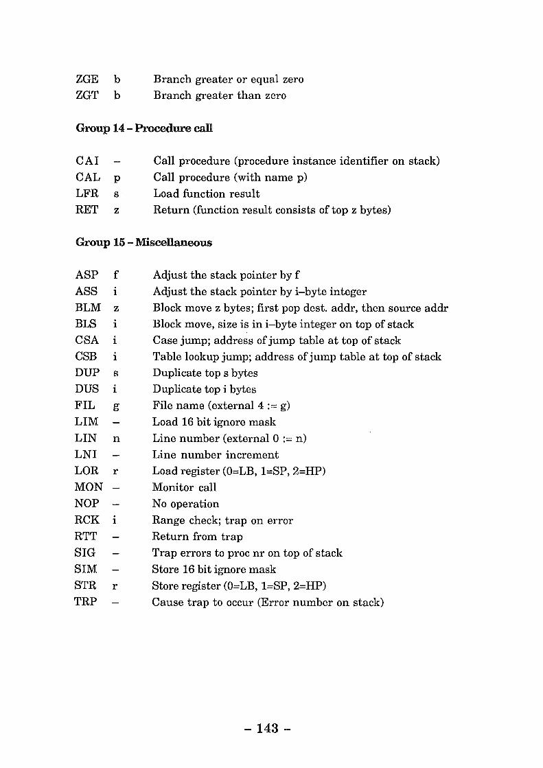
ZGE b ZGT b
Branch greater or equal zero Branch greater than zero
Group 14-Procedure call
CAl CAL p
LFR s RET z
Call procedure (procedure instance identifier on stack)
Call procedure (with name p)
Load function result Return (function result consists of top z bytes)
Group 15-Miscellaneous
ASP f Adjust the stack pointer by f
ASS . Adjust the stack pointer by i-byte integer 1
BLM z Block move z bytes; first pop dest. addr, then source addr BLS 1 Block move, size is in i-byte integer on top of stack CSA . Case jump; address of jump table at top of stack 1
CSB . Table lookup jump; address of jump table at top of stack 1
DUP s Duplicate top s bytes DUS 1 Duplicate top i bytes FIL g File name (external4 :=g) LIM Load 16 bit ignore mask LIN n Line number (external 0 := n) LNI Line number increment LOR r Load register (O=LB, 1=SP, 2=HP) MON Monitor call NOP No operation RCK 1 Range check; trap on error RTT Return from trap
SIG Trap errors to proc nr on top of stack SIM Store 16 bit ignore mask STR r Store register (O=LB, 1=SP, 2=HP) TRP Cause trap to occur (Error number on stack)
- 143-

Key to instruction arguments
Argument Rationale
c 1-word constant
d 2-word constant
1 local offset g global label f fragment offset n positive counter
s object size (word multiple)
z object size (zero or word multiple)
1 object size (word multiple or fraction)
p procedure identifier
b label number
r register number (0,1 or 2)
no operand
-144-

Appendix C Floating Point Accelerator Instruction Set
Floating Point operations
31 28 'Z7 24 Z3 20 19 16 15 12 11 8 7 5 4 3 0
I Cond I 1110 I FP op I FPRn I FPRd I 0 I F lOIFPRm I Cond : As shown in Appendix A FP op : FPU OpCode FPRm,FPRn : FPU operand registers FPRd : FPU Destination register F: Format
FPop : Floating Point Operation 0000 ADD.fmt Add 0001 SUB .fmt Sub 0010 MUL.fmt Multiply 0011 DIV.fmt Divide 0100 SQRT.fmt Square Root 0101 ABS.fmt Absolute Value 0110 MOV.fmt Move 0111 NEG.fmt Negate
Cycles
1000 CVT.S.fmt Convert to single floating-point 1001 CVT.D.fmt Convert to double floating-point 1010 CVT.W.fmt Convert to binary fixed-point 1011 CMP.fmt Compare
Format : Operand type 000 S single precision floating point 001 D double precision floating point 010 W single precision fixed point
Floating Point Unit Register Transfers
Precision Single Double
2 2 2 2 4 5
12 19 23 42 1 1 1 1 1 1 1 1 1 1 1 1 2 2
31 28 'Z7 24 Z3 21 20 19 16 15 12 11 87 543 0
I Cond I 1110 I 0 ILl 0 I Rd I 0 I 0 I1IFPRm I
L :Load I Store bit To FPU=O, From FPU=l
Floating Point Unit Data Transfers
31 28 'Z7 25 24 Z3 22 21 20 19 1615 12 11 87
I Cond I 110 IP(UINIWILI Rn I FPRd I 0 Offset
P : Pre I Post indexing Post=O , Pre=l N : Transfer Length L :Load I Store bit Store=O, Load=l FPRd : FPU register.
- 145-
U: Up I Down bit Down=O, Up=l W: Writeback flag Rn :ARM Base register Offset :Integer addresses offset
0