a parametric study on the electrodeposition of …leung.uwaterloo.ca/group meetings/2003...
TRANSCRIPT
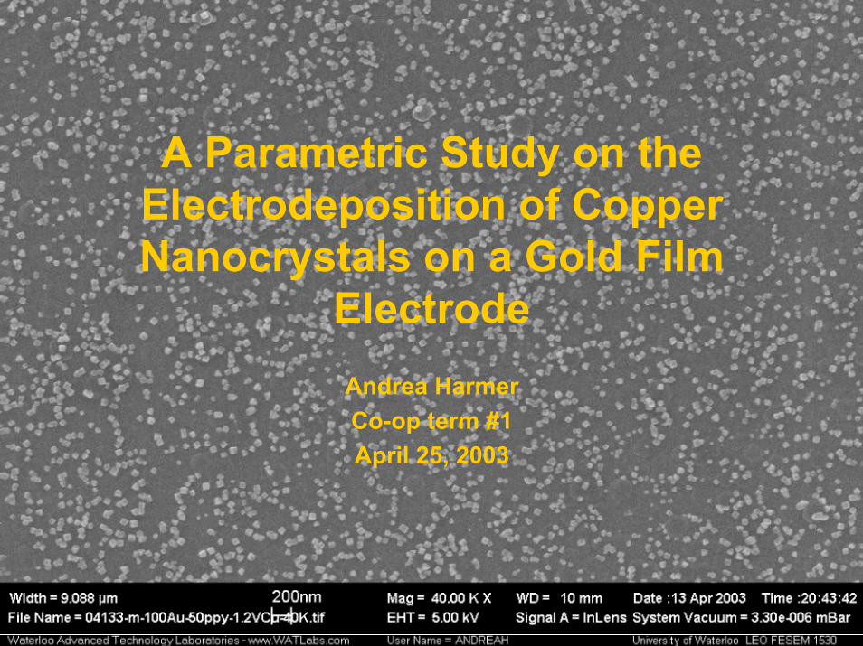
A Parametric Study on the Electrodeposition of Copper Nanocrystals on a Gold Film
ElectrodeAndrea HarmerCo-op term #1April 25, 2003

Outline of Presentation:Introduction
Purpose
General method
Parameters: Experiment and Results
Conclusions/Discussions
Future Work to be Done
Acknowledgements
Resources

Introduction
Old method: True gold electrode
• 3-step process of polishing with alumina powder, ultrasonic bath, and annealing to
1200°C 3X.
• This is done to make it smooth before any deposition can begin.
New method: Gold Film Electrode
• Si is already very smooth.
• Only need to gold plate the Silicon, then you can start experimenting right away !!

Why Gold Film Electrode ?In theory these two electrodes should be equivalent.
Advantages of Gold film Electrode compared to True Gold Electrode:
Smoother - Silicon surface is already smooth and therefore requires no polishing.
Faster - You can do many more deposits in one day because prep-work is almost
eliminated.
Cheaper - The Si wafers last a long time and are not as expensive as the gold
electrodes.

Purpose:
To determine if the gold film electrodedemonstrates the same results as a truegold electrode by examining theexperiment’s parameters.

General Method
Step One: Cutting Silicon
Step Two: Gold Plating
Step Three: Polypyrolle Deposition
Step Four: Cu Deposition
Step Five: SEM Analysis

Step One: Cutting Si Wafers
The Silicon wafers are cut using a diamond cutter into pieces approximately ~ 4mm by 10mm.
The Silicon used was n-typed, phosphorous doped, (001) surface, with one oxidized rough side.

Step Two: Gold PlatingStandard used was 100nm, accomplished with two 50nm deposits or platings.
50nm plating conditions:
Pressure = 50 mt
Current = 25mA
Time = 120sPrinciple:
Once the samples have been loaded, the chamber is evacuated and Ar gas is introduced until the desired pressure stabilizes. Current is turned on and a plasma forms between the argon and gold. Ar atoms accelerate towards the gold and in turn causes gold atoms to be displaced onto the sample.
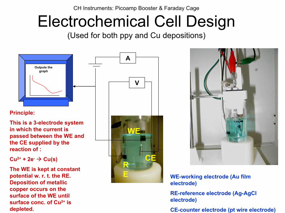
Electrochemical Cell Design(Used for both ppy and Cu depositions)
CH Instruments: Picoamp Booster & Faraday Cage
AOutputs the
graph
V
CERE
WE
Principle:
This is a 3-electrode system in which the current is passed between the WE and the CE supplied by the reaction of :
Cu2+ + 2e- Cu(s)
The WE is kept at constant potential w. r. t. the RE. Deposition of metallic copper occurs on the surface of the WE until surface conc. of Cu2+ is depleted.
WE-working electrode (Au film electrode)
RE-reference electrode (Ag-AgClelectrode)
CE-counter electrode (pt wire electrode)

Step Three: ppy deposition
Polypyrrole (ppy) is a polymer consisting of pyrrolemonomers.
NStandard Ppy Solution:
0.05M pyrrole, 0.1M NaClO4 Experimental set-up:Technique: ChronopotentiometryParameters:
Thickness = 50 nm (standard)
Anodic time = 20s
Anodic current = 1.2mA
Cathodic time = 0.05s
Initial polarity = anodic
High E limit = 1V
Low E limit = 0V
Cathodic current = 0A
20 mL of this solution is put into the cell and bubbled with N2 gas for 20 minutes to remove oxygen. A gold-plated Si wafer is inserted into the clamp holder (as in the picture to the right), and then placed into the electrochemical cell allowing ~0.16cm2 area of the wafer to be in the solution.
All wires are connected to the WE, RE, and CE.
The computer is set up, then the experiment is run after a brief 10s pre-conditioning period.
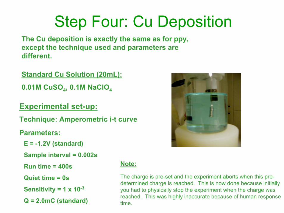
Step Four: Cu DepositionThe Cu deposition is exactly the same as for ppy, except the technique used and parameters are different.
Standard Cu Solution (20mL):
0.01M CuSO4, 0.1M NaClO4
Experimental set-up:Technique: Amperometric i-t curve
Parameters:E = -1.2V (standard)
Sample interval = 0.002s
Run time = 400s
Quiet time = 0s
Sensitivity = 1 x 10⁻³
Q = 2.0mC (standard)
Note:
The charge is pre-set and the experiment aborts when this pre-determined charge is reached. This is now done because initially you had to physically stop the experiment when the charge was reached. This was highly inaccurate because of human response time.
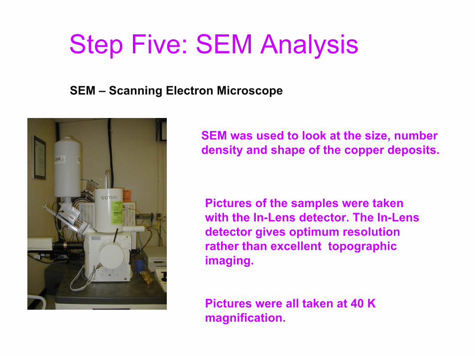
Step Five: SEM AnalysisSEM – Scanning Electron Microscope
SEM was used to look at the size, number density and shape of the copper deposits.
Pictures of the samples were taken with the In-Lens detector. The In-Lens detector gives optimum resolution rather than excellent topographic imaging.
Pictures were all taken at 40 K magnification.

The In-Lens Detector
Secondary electrons are produced as a result of collisions between the incident electrons and atoms within the specimen. Secondary electrons have relatively low energy and are detecting by attracting them to an in-lens detector mounted directly above the specimen.

Parameters: Experiment and ResultsThese experiments were performed on three separate occasions in order to determine if results were reproducible and if trends continued to be true.
The general method outlined earlier was used but changed the parameters accordingly.
The parameters include:Potential
Charge
CuSO4 Concentration
NaClO4 Concentration
Ppy Thickness
Au Thickness

PotentialPrevious results with the true gold electrode:
As potential increases, size of the crystal decreases, number density increases, regular cubes produced between -0.3V to -1.2V.
Experiment:
Varied potential:
-0.2V, -0.4V, -0.6V, -0.8V, -1.0V, -1.2V, -1.4V, -1.6V
Standard Parameters:
100nm Au
50 nm ppy
Solution – 0.01M CuSO4, 0.1M NaClO4
Q = 0.002C or 2.0mC
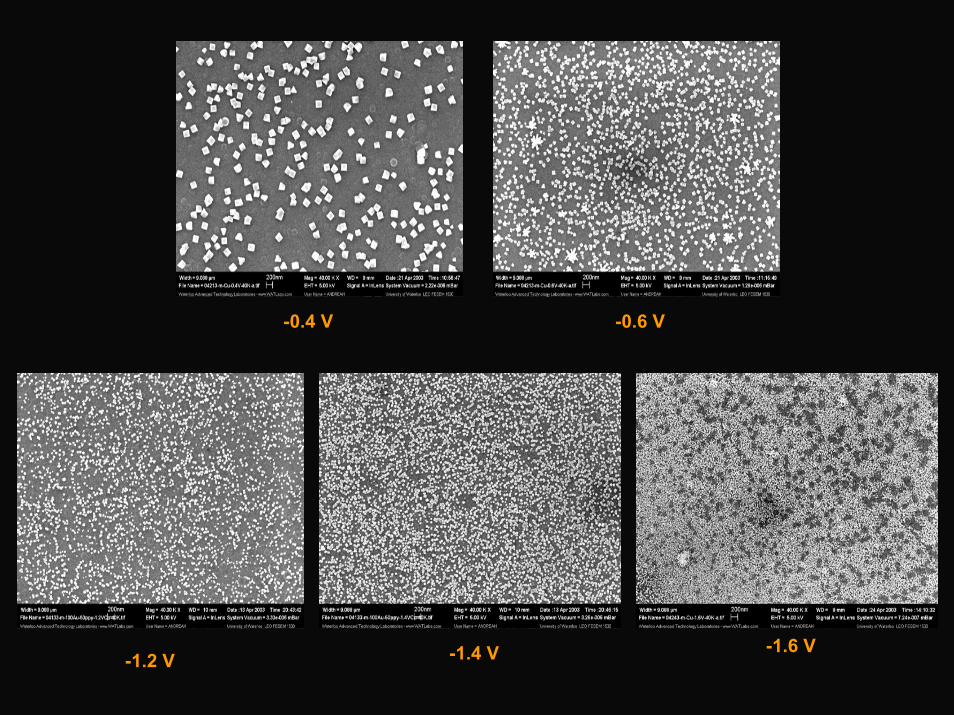
-0.4 V -0.6 V
-1.6 V-1.4 V-1.2 V

Potential Vs. Size of Crystal
0
20
40
60
80
100
120
140
160
180
-2-1.8-1.6-1.4-1.2-1-0.8-0.6-0.4-0.20
Potential (V)
Leng
th (n
m)
Result: As potential is increased, the size of the crystal decreases.

ChargePrevious results with the true gold electrode:
As charge increases (done as time before), cubes were produced between a range of 1.81mC and 9.05mC, or between 5-20s.
Experiment:
Varied Charge:
0.5mC, 1.0mC, 3.0mC, 5.0mC, 7.0mC, 10.0mC,
50.0mC, 100.0mC
Standard parameters:
100nm Au
50nm ppy
Solution – 0.01M CuSO4, 0.1M NaClO4
E = -1.2V

5.0 mC0.5 mC
100.0 mC10.0 mC

CuSO4 ConcentrationPrevious Results with the true gold electrode:As CuSO4 concentration increases, size increases.
Minimum CuSO4 conc. = 0.005M
Experiment:
Varied CuSO4 concentration:
0.001M, 0.005M, 0.01M, 0.02M, 0.05M, 0.1M
Standard parameters:
100nm Au
50 nm ppy
Solution – 0.1M NaClO4 + varied CuSo4 conc.
E = -1.2V
Q = 0.002C or 2.0mC

0.001 M 0.01 M
0.1 M

NaClO4 (electrolyte) ConcentrationPrevious results with true gold electrode:
As NaClO4 concentration increases, nucleation increases which increases the number density, size slightly decreases.
Experiment:
Varied NaClO4 (electrolyte) concentration:
0.01M, 0.05M, 0.1M, 0.2M, 0.5M, 1.0M
Standard parameters:
100nm Au
50 nm ppy
Solution – 0.01M CuSO4 + varied NaClO4 conc.
E = -1.2V
Q = 0.002C or 2.0mC

0.01 M 0.05 M
0.2 M 0.5 M
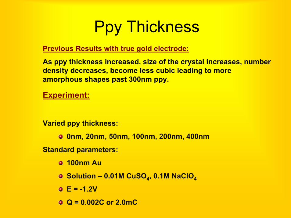
Ppy ThicknessPrevious Results with true gold electrode:
As ppy thickness increased, size of the crystal increases, number density decreases, become less cubic leading to more amorphous shapes past 300nm ppy.
Experiment:
Varied ppy thickness:
0nm, 20nm, 50nm, 100nm, 200nm, 400nm
Standard parameters:
100nm Au
Solution – 0.01M CuSO4, 0.1M NaClO4
E = -1.2V
Q = 0.002C or 2.0mC
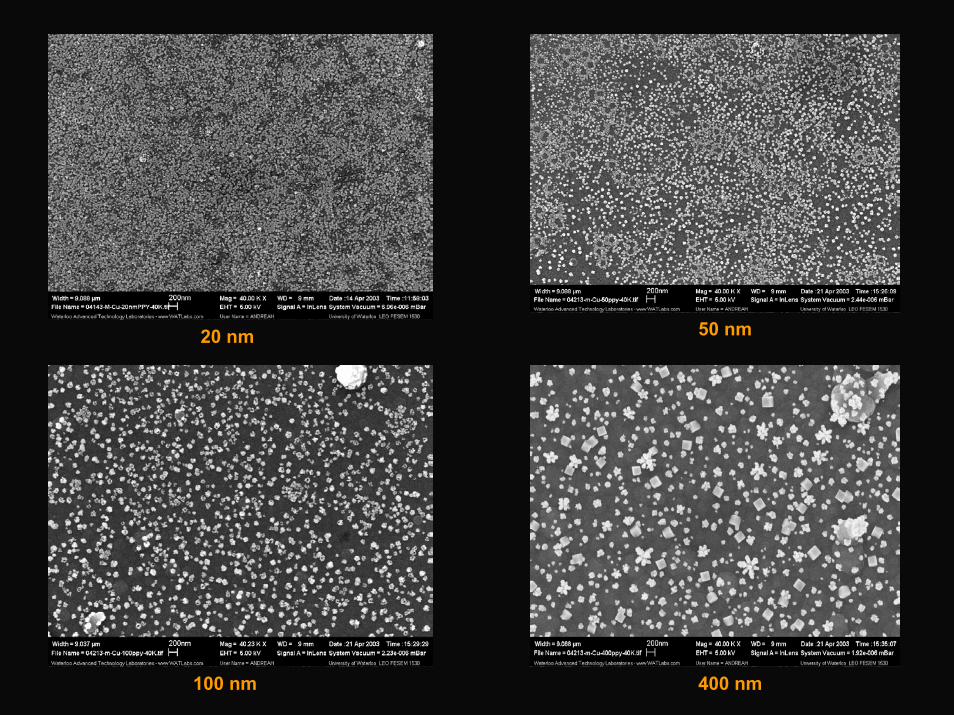
50 nm20 nm
100 nm 400 nm

Au ThicknessPrevious results with true gold electrode:
Since a true gold electrode was used previously there was no parameter for gold thickness.
Experiment:
Varied gold thickness:
0nm, 20nm, 40nm, 60nm, 80nm, 100nm, 150nm
Standard parameters:
50 nm ppy
Solution – 0.01M CuSO4, 0.1M NaClO4
E = -1.2V
Q = 0.002C or 2.0mC

0 nm 20 nm
150 nm80 nm

Discussion
Note:
All pictures were taken at the meniscus of the deposit. The meniscus appears to be the optimum location for getting the results previously found with the true gold electrode. The rest of the deposit area is highly non-uniform.
Possibilities of what may be causing the difference:
1. Orientation of the area to be deposited
2. Possible potential gradient
3. Surface tension at meniscus
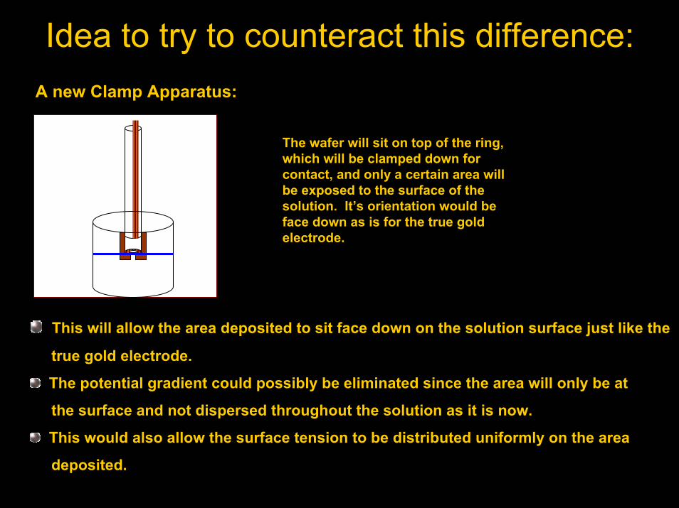
Idea to try to counteract this difference:A new Clamp Apparatus:
The wafer will sit on top of the ring, which will be clamped down for contact, and only a certain area will be exposed to the surface of the solution. It’s orientation would be face down as is for the true gold electrode.
This will allow the area deposited to sit face down on the solution surface just like the
true gold electrode.
The potential gradient could possibly be eliminated since the area will only be at
the surface and not dispersed throughout the solution as it is now.
This would also allow the surface tension to be distributed uniformly on the area
deposited.

Future Work to Be Done
1. As noted on the last slide, the future work would include
making the new holder and testing it out under these same
conditions to see if more uniform and reproducible results
can occur. The problem with the meniscus being the
optimum location of deposition hopefully can be eliminated.
2. Also, this same experiment testing the parameters should
now be done on Ni deposition.

SummaryAs potential and charge were increased, the size of the crystal decreased, while the number density increased. This is more significant with potential. Cubes were produced in the -0.2V to -1.4V range and 1.0mC to 10.0mC range.
As the CuSO4 concentration was increased, the shape became more polyhedral and bigger. No conc. Threshold was noted as crystals were found at the lowest conc., though very small.
As the NaClO4 concentration was increased, not much change was noted at low or high concentrations. Moderate concentrations appear to be highly non-uniform.
As the ppy thickness was increased, size of the crystal increased, number density decreased, but you start to get a mixture of cubes and amorphous shapes even after 100nm.
As the Au thickness was increased, density number increased as well as a more regular cubic shape was noted.
The Gold Film Electrode produced the same basic trends and some new insights as with a True Gold Electrode, though with some variations as to the reproducibility of the results. However as mentioned before this could be attributed to how the apparatus is set-up. Therefore it will be very interesting to see the results taken with the new design of clamp.

AcknowledgementsXiang and Nina !!
Xiaojing and Tong !!
I just want to thank all these people who have helped tremendously through my co-op term, were always supportive, and willing to help explain anything.
ResourcesDick, K., “Systematic Study of Parameters in Electrodeposition of Cu Nanoparticles on Polypyrrole Substrate”, 3B work report, University of waterloo, 2001.
Oskam, G., Searson, P. C., 2000, J. Electrochem. Soc., 147, 2199
Sadki, S., 2000, J. Royal Soc. of Chem., 29, 283
Southampton Electrochemistry Group. “Instrumental Methods in Electrochemistry”. Toronto: John Wiley & Sons. 1985.

My Presentation is OVER !!!