a new parallel test approach for large memories
TRANSCRIPT

A New Parallel TestApproach for Large
Memories
Thirumalai SridharTexas Instruments
W ith the advent of VLSI technology, the size of memory_ circuits has increased rapidly. Currently, 64K and 256KRAMs are commercially available, and 1M RAMs will soon fol-low. The test time and cost of a memory chip-directly dependenton a chip's size-are also rising. Also, in microcomputers,' the testtime and cost are dominated by their on-chip memories. Thistrend will continue in the future.Only recently have a few researchers reported their work on
improving the testability of memory circuits using on-chip testlogic. Their main focus is on adding test logic to execute a memorytest algorithm and verify the test response on the chip itself.
While simple comparators were proposed to verify the test re-sponses from memory arrays, Kinoshita and Saluja2 have usedspecial data compaction as dictated by their test procedure. Theircompaction consists of special counters that compute certaincount functions operating on the memory array output words, andthe presence of faults is detected by comparing the contents of thecounters with expected values.
In the past, more refined and more efficient memory test algo-rithms than the conventional ones (such as Marching l's and 0'sand Galpat3) were suggested to reduce the test times.4'5 You andHayes6, in addition to using their own efficient test sequence for a64K dynamic RAM, partition the memory array into two identi-cal partitions and test them concurrently to save test time. Simi-larly, four partitions are used in a 1M DRAM to reduce test timeby a factor of four.7
Also, to reduce overall test time and cost, many memory chipscan be tested in parallel, sharing the resources of a single testsystem.8
nA'n74a'74'TC O Ulctflfb-nIA A 15August 1986
E_ E_ E_
V/-tV-/-t1_,/0U/V0VV-.1J.VV1.VV - -o. .---

Figure 1. Architecture of a large memory. Figure 2. Two methods of integrating PSAs in large memories.
In contrast, this article presents a new
approach using on-chip logic to reducethe test time both for a given memory testalgorithm and for a single chip. This ap-
proach relies on parallel signature analyz-ers (PSAs).A PSA is a multiple-input linear feed-
back shift register (LFSR) used to com-
press test response data in a digital circuitunder test.9 Instead of verifying the re-
sponse to every test pattern, one can com-
press the responses on chip in a PSA andverify only the final contents (its signa-ture) of the PSA.
In processor chips, PSAs are ideallysuited to monitor internal buses and nodesto aid both conventional testing using tes-ters and self-test.10 Recently, PSAs havealso been used in commercial products.They are easily combined with scan de-signs to realize simple self-test techniques.PSAs have also been proposed to test othercircuits such as PLAs. Furthermore, sig-nature analysis techniques have been ap-
plied to on-line (or concurrent) checking ofprocessors and systems.
Although the parallel test method is dis-cussed in this article in the context of
memory chips, it is equally applicable toVLSI chips, such as microcomputers, withlarge embedded memories.
Proposed method
Consider an N X d memory chip con-
taining Nd memory cells organized as Nrandomly addressable words of size d bitseach. In such a chip, we can read/write thecontents of each word via the d data I/Opins. Therefore, at any time, we can access
only d memory cells in parallel.In the proposed scheme, called parallel
testing using PSAs, a larger number ofmemory cells are accessed by PSAs at thesame time (in parallel) than is possible viathe existing I/O pins. In an N X d memo-ry, it is possible to monitor the contents ofp memory cells (or write data into them) inparallel in two ways, where p > d.The cell output signals coming out on
the bit lines (after amplification by sense
amplifiers) can be accessed either just be-fore or inside the column decoder. In thefirst case, maximum possible parallelism isachieved, since every bit line will be moni-tored. If the accessing is done after a cer-
tain stage in the column decoder (the sec-
ond case), then only a fraction of the totalnumber of bit lines (but still more than d)can be monitored.
Figure 1 depicts a typical architecture ofa large memory such as 256K X 1. (Thesizes of the blocks shown in the figure are
for a 256K X 1 DRAM,I i and each of theeight cell array sections contains 32Kmemory cells.) The memory architectureconsists of four quadrants of cell arrays
accessed by row and column decoders as
shown.The row decoders access vertical lines,
called word lines, one in each quadrant fora given address. All cells connected to theselected word line transfer their contentsonto the horizontal lines called bit lines.The bit-line signals are amplified by thesense amplifiers and are available alongthe entire length of the bit lines, extendingfrom the outside edges of the quadrants tothe column decoder. The column decoderselects one bit-line signal from each quad-rant and sends four I/O signals to the finalone-of-four decoder.
In such memory circuits, the bit linescan be accessed in two ways. All bit lines
IEEE DESIGN & TEST
(a) *t
Bit Lines Scan-out Data/ Bus (Quotient)
SA SA
rSe~~~~~~tell SA SAArray
Scan-in Data
(b) (Fron Pin)
I
16

Figure 3. A block schematic of the proposed PSA.
can be directly accessed, depending on thelayout considerations, either at the outsideedges of the quadrants or just before thecolumn decoder at the inside edges of thequadrants. An alternative is to indirectlyaccess only a fraction of the bit lines after a
certain stage of the column decoder. In theproposed method, bit lines are accessedwith PSAs.
Suppose a k-bit PSA is used to access p
memory cells via p bit lines, where k is thenumber of master/slave flip-flop (or sim-ply a one-bit register) stages in the PSA, k' p and p > d.Figure 2 illustrates the above two meth-
ods of accessing bit lines using PSAs. InFigure 2a, a large PSA accesses all bitlines, whereas a smaller PSA accesses a
fraction of the bit lines, as Figure 2bshows.
In the latter case, the PSA is placed af-ter a certain stage of the column decoder.For convenience, p will usually be a power
of two, as are N and d. For example, ifthere are 512 bit lines (as in Figure I) com-ing into the column decoder, then p can be512, 256, 128, 64, 32, 16, or 8.The corresponding PSA size k should be
at least p, since one flip-flop stage of thePSA is required to monitor one bit line.However, k can be selected to be greaterthan p to enhance the probability of detect-ing errors in the data compressed by thePSA. If k = p, then every flip-flop stage inthe PSA monitors exactly one bit line. Onthe other hand, if k > p, some selected(k-p) flip-flop stages in the PSA do notreceive any parallel data input.As shown in Figure 2a, as an alternative
way to access all bit lines, the PSA can belocated at the other edge of the quadrants(that is, at both sides of the column decod-
er). The scan-in and scan-out lines fromthe PSAs can be connected to existing datapins. (The scan-out data is also referred toas the quotient. The name "'quotient" wascoined in the context of the polynomial di-vision process in which linear feedbackshift registers were first used.)
These two methods of using PSAs to ac-
cess the bit lines (either directly or indi-rectly through a portion of the column de-coder) are easily applied to memory arrayarchitectures other than the one shown inFigures 1 and 2 (which was chosen solelyto illustrate the concepts). (Unless statedotherwise, both approaches, as shown inFigures 2a and 2b, apply equally to theremainder of the article.)
PSA structure and operation modes.Figure 3 shows a block diagram of the pro-
posed PSA to test large memories. It con-
sists of k (for simplicity, k = p here) mas-
ter/slave flip-flop stages with their inputsconnected to the parallel input lines (eitherthe bit lines or some internal data lines ofthe column decoder) through an exclusive-OR gate.The other input to this gate is connected
to the output of the previous flip-flopstage. (A flip-flop stage is a combination ofmaster and slave latches clocked by twononoverlapping clocks.) There are addi-tional exclusive-OR gates at selected feed-back points, as the figure shows. The feed-back points are dictated by the feedbackpolynomial used for the data compression.The two-way mode switch and the write
switch together define the PSA's operationmode to be one of the following threemodes:
Signature/read mode. The mode switchis in the Monitor position and the write
switch is open. During memory-read cy-cles, p memory cells are monitored in par-allel. At the same time, the PSA compress-es the p-bit data read and generates a newk-bit signature. This signature (and, ifnecessary, the quotient bit which is themost significant bit) can be used to deter-mine whether the memory circuit is faulty.Thus, all Nd memory cells can be read inNd/p cycles instead of in the normal Ncycles without the PSA.
Write mode. The mode switch is in anyposition and the write switch is closed. Thisis the opposite of read mode. The contentsof the PSA are written into thep cells con-nected to it, during the memory-write cy-cles, and the PSA contents are unchangedby not clocking the slave latches. Thus, allNd/p p-bit words can be written with thesame p-bit pattern in Nd/p write cycles.The write data itself is obtained during thescan mode (as discussed below).
Scan mode. The mode switch is in theScan position and the write switch is open.This mode is used for communication be-tween the PSA and the outside world. In it,the PSA functions as a simple k-bit shiftregister. At the end of a test experiment,the contents of the PSA (the signature)can be scanned out through the scan-outpin using k scan cycles. The scan-in pin isused to load the PSA with any k-bit word.This lets known data be written into the pcells in the write mode described above. Ifseparate pins are used for input and out-put, both scan-in and scan-out of datacould be achieved concurrently in only kcycles.The above operation modes help to effi-
ciently test the memory circuit.
August 1986
Write Switch B Bp-i B0
I + j + FF + IO~~~~~~~~~~~~1--ScanScan FF Fn _ _ + I nOut
Monitor L J
Scan 91
I Mode Switch
Last Stage Feedback Point First Stage
17

Parallel test procedure
The fundamental idea behind the use ofPSAs to test large memory circuits is toreduce the total test time by reducing thenumber of read and write cycles during theparallel test.Any existing or new test algorithms can
be used here for PSA-based parallel tests.For example, conventional memory test al-gorithms such as Checkerboard, March-ing l's and 0's, Walking l's and 0's, andGalpat3 can be used successfully.
Modifying a test algorithm. Consideragain an N X d memory circuit with pmemory cells accessed by a k-bit PSA asshown in Figure 2. During the parallel test,this memory can be considered to be orga-nized as N/F words of size p bits each,where F = p/d, instead of the usual Nwords of size d bits each. Each N/F p-bitword can be accessed via the k-bit PSA.Such p-bit words are called PSA-accessi-ble words, or p-words.
Therefore, any memory test algorithm ismodified to access the p-words instead ofthe normal d-bit pin-accessible words.That is, the target word during the paralleltest will be a p-word on which a read orwrite operation is performed. Figure 4 il-lustrates this for the Marching l's and 0'salgorithm.
Figure 4 gives the original and the modi-fied algorithms, which are self-explana-tory. In step 1, the background data iswritten with the PSA in its write mode us-ing N/F memory write cycles (after k cy-cles are spent in the scan mode to scan inthe write data). The scan-in operation instep 2b, before the actual write cycle, isoptional.At this stage, the contents of the PSA
(the current signature), say SI, can itselfbe used to derive the all-one write datawith a simple translation: inverting select-ed bits in SI. This is feasible because thedata sequence monitored and compressedby the PSA during the read cycles in theloop of step 2 is periodic. Therefore, thePSA can be designed so its signature se-quence is also periodic, like SI, S2, SI,S2, ... in the fault-free case.
If the current signature of the PSA isitself used to derive the write data, there isno need to use k scan cycles to scan in therequired write data from outside. This sav-ing is crucial in improving the test timereduction factor for linear memory test al-gorithms whose complexity is O(N)that use interleaved memory read andwrite cycles in a loop, as in steps 2 and 3 of
1. Write background of zeroes
2. For i:= 1 toNdoa. Read all-zero from word(i)b. Write all-one into word(i)c. Read all-one from word(i)
3. Fori:=ltoNdoa. Read all-one from word(i)b. Write all-zero into word(i)c. Read all-zero from word(i)
4. Repeat for background of ones
Test length L = 14N(a)
1. (Write background of zeroes)a. Scan in all-zero in PSAb. Fori:= I toN/Fdo
Write PSA contents into p-word(i)2. Fori:= l toN/Fdo
a. Read all-zero from p-word(i)b. {Scan in all-one into PSA} (optional)
Write PSA contents into p-word(i)c. Read all-one from p-word(i)
3. Fori:= ltoN/Fdoa. Read all-one from p-word(i)b. (Scan in all-zero into PSA} (optional)
Write PSA contents into p-word (i)c. Read all-zero from p-word(i)
4. Repeat for background of ones
Test length Lp = 2(3k+ 7N/F)(b)
Figure 4. Marching l's and O's algorithm: (a) original and (b) modified.
the Marching l's and 0's algorithm.On the other hand, the scan-in opera-
tion, before the PSA write cycle, need notbe eliminated in the case of any O(N2) al-gorithms such as Walking l's and 0's andGalpat. In such cases, the extra scan cyclescontribute very little to the test length.This is evident from the modified Walkingl's and 0's algorithm shown in Figure 5.The foregoing discussions are valid even
when the all-one and all-zero data patternsused in Figures 4 and 5 are changed to anyother patterns, such as 0101... and 1010....
Test length. It is evident from the modi-fied algorithms of Figures 4 and 5 that thenumbers of memory read and write cyclesare both significantly less than those in theoriginal algorithms. Using the PSA in thewrite mode (see step 1 of Figure 4b), thenumber of memory write cycles is reducedfrom N to N/F, but additional k cycles arerequired (step I a) to scan in the write data.
However, k is quite small compared toN/F, and these k scan cycles could be runfaster than the memory read/write cycles.Similarly, the PSA read mode helps re-duce the number of memory read cycles insteps 2 and 3 of Figure 4.
For the Marching l's and 0's algorithm,the test length L (in number of memorycycles) without the PSA, according to theconventional approach (Figure 4a), is14N. With the PSA (Figure 4b), the testlength Lp will be 2[(k+N/F) + {k+N/F(l+l+1)} + {k+N/F(l+l+l)}],with-out the optional scan-in operations in steps2 and 3 and with additional k cycles (not
indicated in the figure) to properly initial-ize the PSA before the two loops to realizeperiodic signature sequences.
Lp will simplify to 2(3k+7N/F). Forlarge N, the test length will therefore re-duce from 14N to 14N/F. Thus, the reduc-tion factor will be very close to F, which isequal to p/d. However, with the scan-inoperations of steps 2 and 3 (when the newwrite data is not derived from the contentsof the PSA but instead is scanned in fromoutside), Lp will be 2[(k+N/F) + N/F(l+k+l+l) + N/F(l+k+1+1)].With k = p and d = 1, this will simplify to2(2N+k+7N/k). For large N, the reduc-tion factor in this case will be at most 3.5,which is far less than F. This highlights theneed for generating periodic signaturesequences.
Test lengths in the case of the Walkingl's and 0's algorithm of Figure 5 will be asfollows: The original length L will be2N(N+ 3), and the modified length Lp is2[N2/F2 + N/F(2k+3) + k]. For largeN, the test length will diminish from 2N2to 2N2/F2, making the reduction factor F.
In general, the test times due to O(N)and O(N2) algorithms can be reduced by afactor ofF and F2, respectively, where F =p/d. In other words, if T is the original testtime, then the new test time with the useof a PSA will be very close to T/F orT/F2. Thus, the test times for large memo-ry circuits, such as 256K and 1M RAMs,can be significantly reduced.
Parallel test mode. Any modified algo-rithm is executed in a special parallel test
IEEE DESIGN & TEST18

1. Write background of zeroes
2. Fori: = 1 toNdoa. Write all-one into word(i)b. Read all-zero from word(j),
for all j =# ic. Read all-one from word(i)d. Write all-zero into word(i)
3. Repeat for background of ones
Test length L = 2N(N+3)
(a)
1. (Write background of zeroes)a. Scan in all-zero into PSAb. For i: = 1 to N/F do
Write PSA contents into p-word(i)2. For i := I to N/F do
a. Scan in all-one into PSA,Write PSA contents into p-word(i)
b. Read all-zero from p-word(j),for all j # i
c. Read all-one from p-word(i)d. Scan in all-zero into PSA,
Write PSA contents into p-word(i)3. Repeat for background of ones
Test length Lp 2[N2/F2 +N/F(2k+3) + k]
(b)
Figure 5. Walking l's and 0's algorithm: (a) original and (b) modified.
mode. The memory chip is tested as usualusing an automatic test equipment or, sim-ply, a tester.
First, the parallel test mode is itself in-voked using either a special test pin orovervoltage detection circuitry to detect ahigh voltage like 12V on an existing pin.Once the device is in this mode, we canredefine the function of many existing pinsfor the parallel test. For example, two orthree pins required to control the functionof the PSA can be some of the unused ad-dress pins.
This is feasible because, for parallel test-ing, we need to address only N/F p-wordsinstead of N normal d-bit pin- accessiblewords. Also, if d > 1, then d-1 or d-2data pins are free to be redefined, since atmost two data pins are required to scandata in and out of the PSA. Therefore, it ishighly unlikely that any new pins are re-quired to implement the parallel test.
After the parallel test mode is entered,the modified test algorithm is executed.PSA is initialized to an initial state. Itscontents are scanned out just before newwrite data is scanned in from outside andalso at the end of the algorithm. Everytime the signature is read out, it is verifiedby the tester with the expected value todetermine whether the memory circuit un-der test is faulty. Also, the pin used to scanout the PSA contents can be continuouslymonitored by the tester to verify its quo-tient-bit stream. The end of the paralleltest mode is signalled by applying a highvoltage on the same pin.
Note that the foregoing parallel testingwill test all Nd memory cells and the por-tion of the column decoder present beforethe data lines monitored by the PSA. Theremainder of the column decoder shouldbe tested separately in the regular modewithout using a PSA. This can be achievedwith a short test sequence whose length isnegligible compared to the one used in theparallel test mode to test the memory cells.
For example, the Marching 1's and 0'stest can be used on a particular row of cellsto test the column decoder and the I/Obuffers. Here, the traditional method ofusing the I/O data pins to write test dataas well as to verify the data read out isemployed and the PSA is ignored. The testlength of such a sequence will be 14Nr(Figure 4a), where Nr is the number ofcells in a row.
Furthermore, only a fraction of the col-umn decoder after the PSA needs to betested this way, so the number of cells in-volved would be a fraction of Nr, which isvery small compared to N. Similar addi-tional test sequences are required to com-plete testing the entire chip, where redun-dant columns have replaced bad columns.
Using p-words as targets. The underly-ing principle in reducing test length in theproposed parallel test approach is that thetarget word for both read and write opera-tions has more cells than the normal pin-accessible word. This basic differencebrings up the issue of intercell interactionsand cell-to-cell transitions.
In the traditional approach, complextests such as the row/column disturbtest, Walking l's and 0's, and Galpat-detect any cell coupling errors, addresstransition errors, and the like. The PSAapproach preserves the detection capabili-ties of all such test algorithms as far asinteractions and transitions between cellsof different p-words are concerned.
Particular data patterns that must bestored in the neighboring cells of a p-wordcan be easily established by properly se-lecting the write data patterns for a givenp-word and its neighboring p-words. Ifnecessary, we can use the PSA's shift ca-pability to generate the desired data pat-tern. However, the parallel test techniquedoes not guarantee the detection of anycoupling or transition errors between cellsof the same p-word but this problem iseasily resolved.
Consider the Walking l's and 0's algo-rithm of Figure 5, which is representativeof algorithms that detect cell coupling er-rors or address transition errors. All errorsdue to interactions between cells of differ-ent p-words are detected by the modifiedalgorithm of Figure 5b. To detect all errorscaused by interactions between cells of thesame p- word, we propose to add a new testsequence, say step 2e, to the existing step 2sequence. (For simplicity, d is assumed tobe 1.)
In step 2e, we propose to test the interac-tions between cells of the selected p-word p-word(i) as follows: There are pcells in p-word(i). Write an opposite datavalue into the target test cell only as a pin-accessible cell using the traditional normalwrite cycle without disturbing the contentsof the remaining p-1 cells in p-word(i).Then read all p cells of p-word(i) using
one parallel read cycle and compress the p-bit data in the PSA. This read cycle willverify whether the previous write cycle hasdisturbed any of the remaining p-1 cells.
Finally, restore the data stored in thetarget test cell by again using a normalwrite cycle. Repeat this sequence, consist-ing of three cycles, for all p cells in p-word(i). With this new step, interactionsor transitions between every cell includ-ing the cells within any p-word- would betested when step 2 has completed. If neces-sary, the additional test sequence can beapplied separately at the end of the exist-ing Walking l's and 0's test sequence.The additional test sequence is of length
2{N/p}{p( I + 1+ I)}, which simplifies to6N. This is obviously quite small comparedto the existing length Lp shown in Figure5b. Thus, even with the additional se-
August 1986 19

quence, the test time to execute the modi-fied Walking l's and 0's algorithm is stillless by a factor of F2.The foregoing discussion is easily ex-
tended to any other test algorithm, such asGalpat, used to test coupling errors, ad-dress transition errors, and the like.
Redundancy techniques. It is well-knownthat row- and column-redundancy tech-niques improve the early production yieldof large memory circuits. The presence ofredundancy circuits does not affect theparallel test method when the memory cir-cuit is not repaired with any redundantrows or columns. The parallel test withPSAs can be used even in memory circuitsrepaired by replacing bad rows and col-umns with the redundant ones.Row redundancy has no effect on paral-
lel testing because the PSA monitors thebit lines (or the columns) and does not de-pend on whether a regular row or a redun-dant row is selected. Furthermore, the badrow is completely disabled by the redun-dant row selection logic.On the other hand, column redundancy
influences the parallel testing. Depending onwhere the PSA is used, it may receive un-known or unpredictable data from a badcolumn in a repaired memory chip. This willinvalidate the parallel test, since the correctexpected signature will be unknown.A simple approach to this problem
would be to place the PSA only after thecolumn decoding stage that selects the re-dundant columns (the stage where datafrom redundant columns, if programmed,is selected instead of the bad columns).Thus, the PSA will get no bad data fromthe replaced bad columns.A potential drawback is that the column
decoding stage that selects any redundantcolumn will usually be toward the end,where the number of data lines availablefor the PSA to monitor is small. This willreduce the parallelism obtainable duringthe parallel test.
For example, suppose the redundantcolumns are multiplexed at the last stageof column decoding, where the final one-out-of-four selection is made, as in Figure1. Then the ratio p/d will be only four.However, the parallelism can be increasedby moving the redundant column selectionto an earlier column decoding stage. Thismay pose other problems, such as wiringand additional silicon area.
Another approach might be to integratethe PSA at an early stage of the columndecoder and keep the redundant columnselection to a later stage. Suppose the PSA
is placed after a one-out-of-n decoding ofbit lines. In other words, every bit in thePSA will receive data from one out of n bitlines. The parallel test will test all the bitlines before any redundant column is pro-grammed for selection.
However, after a redundant bit line isselected to replace a bad one, some jth bitposition of the PSA can receive corrupteddata from the bad column connected to itevery time the bad column is addressed.Therefore, parallel test cannot be appliedto a repaired memory because the expect-ed signature will be unknown. At the sametime, potentially good data from the select-ed redundant column will be multiplexedafter the PSA.One solution is to make the expected sig-
nature a known value by forcing a knowncorrect value into the affected bit positionof the PSA. (If the known value can beobtained from the selected redundant col-umn, this approach would be the same asthe previous one.) Usually, the known val-ue could be constant 1 or 0, obtainedthrough either some fuse-blown circuit ora small multiplexing logic. This will alsoprevent data coming from (n- I) good bitlines also connected to the same jth bit po-sition of the PSA.With this approach, all these bit lines, as
well as the selected redundant column,must be tested outside the parallel testmode using regular methods. However,this will not add much to the total testtime.
Finally, if either of the above two ap-proaches is not feasible or acceptable, wecan completely forego testing of the re-paired chips in the parallel test mode andinstead test them with conventional meth-ods. However, all nonrepaired chips can beefficiently tested using the PSA, and thisapproach can still reduce the overall cost oftesting hundreds of a mixture of repairedand nonrepaired chips.
Effectiveness
The inherent data compression involvedin using a PSA to monitor test responsesdetermines the test quality, in addition tothe quality determined by the test algo-rithm used. With the PSA, the quality canat best be that of the test algorithm. Withthe past results and experience,9"0 it is safeto claim that the probability of any loss offault information due to the data compres-sion in the PSA is very small.
In the past, we found that commonstuck faults in the memory cells, bit linesand word lines, decoder faults, and shorts
between adjacent lines are all detected justby verifying the final signature of a PSA of16 bits or more in size. As an example,'0simulation results indicate that all bit col-umns' stuck-at- 1 faults in a 128X 8 memo-ry circuit are completely detected bychecking the final eight-bit signature.
Monitoring the quotient bit. It is knownthat the error detection capability of largePSAs is quite high when only the final sig-nature is verified. However, the error de-tection capability can be significantly en-hanced by monitoring the quotient bit ofthe PSA in addition to verifying the finalsignature.9
Monitoring the quotient bit is straight-forward, since the most significant bit ofthe PSA is connected to an I/O pin to scanout its signature. Therefore, the alreadyavailable quotient data can be continuous-ly verified by the external tester by moni-toring only one output pin.
Repetitive patterns. In the case of mem-ory test algorithms, the test data patternsare repetitive. Therefore, the data com-pressed by the PSA in the proposedscheme is also repetitive. For example, inthe case of the Marching l's and 0's algo-rithm, the data patterns read from thememory (in the two loops of steps 2 and 3of Figure 4) will be alternate all-one andall-zero. The data is periodic with the peri-od equal to two. When the parallel databeing compressed by a PSA is periodic, itis intuitive to expect the signature (thePSA contents) sequence to be periodic aswell.
However, our simulation study indicatesthat this intuition is not always true. Sever-al simulation examples indicate that thefollowing conjecture is true, but it wasneither proved to be true for all casesnor could it be disproved with acounterexample.Our conjecture was that for a k-bit PSA
with a maximal-length feedback polyno-mial, there exists one and only one initialstate that produces a periodic signature se-quence of the same period as the paralleldata input being compressed.
For example, consider an eight-bit PSAwhose feedback polynomial is X8 + X5 +X3 + X2 + 1, with alternate all-zero andall-one as the data sequence being com-pressed. For the initial state 1 1001 100, theperiodic signature sequence will beSl,S2,Sl,S2, ..., where SI = 01100110and S2 = 11001100. The signature se-quence will not be periodic once the initialstate is changed to any other value.
IEEE DESIGN & TEST20

Figure 6. A MOS implementation of the PSA.
An analytical approach to determiningthe initial state, if one exists, that will gen-erate a periodic signature sequence ap-
pears to be feasible but needs to be ex-
plored. The theory on shift-registersequences presented by GolombI2 couldhelp develop such an approach. In the ab-sence of any analytical solution, the onlyalternative is simulation.
It is obvious that periodic signature se-
quences always result in periodic quotient-bit streams but the converse is not true:some nonperiodic signature sequences can
yield periodic quotient-bit streams. There-fore, it will be interesting to see whetherfaults of interest in memory circuits willdestroy this periodicity. If so, it will guar-
antee the detection of all such faults.Another advantage of generating peri-
odic signature sequence is that the currentcontents of the PSA can be automaticallyused (as is, or if necessary, with a simpleconversion) as write data if there are any
write cycles between read cycles in the testloop. This will help reduce the test length,as in the Marching l's and 0's algorithm.
Periodic signature sequence is not re-
quired for any significant reduction in thetest lengths of any O(N2) algorithm and ofthose O(N) algorithms, such as Checker-board, that do not interleave memory readand write cycles in a loop.
Furthermore, a periodic signature se-
quence simplifies the problem of generat-ing expected signatures and quotient-bitstreams. This is especially useful to pro-
gram an automatic pattern generatormodule in a memory tester when signature
is monitored at regular intervals or whenthe quotient-bit stream is continuouslymonitored. It significantly reduces theamount of test data required to be stored.Storing only the final signature (and some
intermediate signatures) is trivial.If for some reason the expected se-
quences are not periodic, large test datawill pose a problem when we decide to veri-fy the quotient bit. One solution is to buildthe PSA circuit either inside or outside thetester and let the circuit generate the ex-
pected quotient.
Application to realmemory circuits
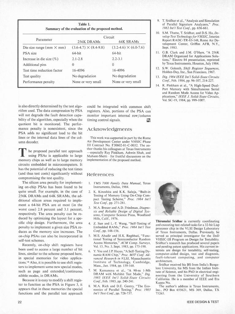
We have studied two classes of memorychips for the application of the proposedmethod: 256K DRAMs and 64K staticRAMs."113
Figure 6 shows a MOS implementationof the ith flip-flop stage of the PSA in Fig-ure 3. The two control signals SIG and Cdefine one of the PSA's three operationmodes. The signals HI and H3 are two non-
overlapping clocks, while Hw is used duringmemory write cycles to enable data fromthe PSA onto the bit lines at proper time.A few additional exclusive-OR gates maybe required between some of the PSAstages to implement the feedback polyno-mial (see Figure 3).
Using 2-,um design rules, the one-bitflip-flop stage of Figure 6 can be built in anarea of about 50,m X 60,tm. Usually,interconnects between the PSA and the ex-
isting logic with which it interacts will add
significantly to the additional area re-
quired. One way of accounting for this is toincrease the height of the one-bit stage to a
fixed size to accommodate interconnectsand then allow the width to grow accord-ing to the PSA size. In our study, a heightof 100 ,um was found to be adequate.
Usually, the PSA is laid along the lengthof the column decoder (see Figure 2), in-creasing the column decoder width (theside perpendicular to the bit lines) by 100gm, the fixed height of the PSA. A goodestimate of increase in die size of the chipwould be to add 100 zm to the side of thechip perpendicular to the bit lines. Thisapproach has been used in the evaluationof the silicon area penalty or the increasein die size. For simplicity, redundant col-umns are not considered here.
Table I summarizes the results of theevaluation. The range of increase in siliconarea (or the die size) corresponds to therange of original (without the PSA) diesizes considered. We have attempted no
optimization in the layout because chipsfrom different vendors were involved. Thearea estimate is based on a conservativeapproach (as discussed above). The esti-mates of additional pins, test time reduc-tion, and test quality are straightforwardand follow directly from the earlier discus-sions. Test time reduction range is depen-dent on the complexity of the memory testalgorithm used and on the value of F.
For example, in the case of a 256K X IDRAM, with a 64-bit PSA, test time re-
duction is 64 for O(N) algorithms, whilefor a 64K X 4 DRAM it is 16. Test quality
August 1 986
FF.
i -1
To BitLi nes(For WritingData)SIG
EXOR B i9FF1-1 tMode Master Slave
I
21
9. T. Sridhar et al., "Analysis and Simulationof Parallel Signature Analyzers," Proc.1982 Int'l Test Conf., pp. 656-661.
10. S.M. Thatte, T. Sridhar, and D.S. Ho, De-velop Test Technologyfor VHSIC, InterimReport RADC-TR-83-148, Rome Air De-velopment Center, Griffiss AFB, N.Y.,Sept. 1983.
11. G.B. Clark and J.M. O'Hare, "A 256KDRAM Organized for Applications Solu-tions," Electro 84 presentation, reprintedby Texas Instruments, Houston, July 1984.
12. S.W. Golomb, Shift Register Sequences,Holden-Day, Inc., San Francisco, 1967.
13. Dig. 1984 IEEE Int'l Solid-State CircuitsConf, Feb. 1984, pp. 96-107, 214-227.
14. R. Pinkham et al., "A High-Speed Dual-Port Memory with Simultaneous Serialand Random Mode Access for Video Ap-plications," IEEE J. Solid-State Circuits,Vol. SC-19,1984, pp. 999-1007.
is also directly determined by the test algo-rithm used. The data compression by PSAwill not degrade the fault detection capa-
bility of the algorithm, especially when thequotient bit is monitored. The perfor-mance penalty is nonexistent, since thePSA adds no significant load to the bitlines or the internal data lines of the col-umn decoder.
T he proposed parallel test approachusing PSAs is applicable to large
memory chips as well as to large memorycircuits embedded in microcomputers. Ithas the potential of reducing the test times(and thus test costs) significantly withoutcompromising the test quality.The silicon area penalty for implement-
ing on-chip PSAs has been found to bequite small. For example, in the case of256K DRAMs and 64K SRAMs, the ad-ditional silicon areas required to imple-ment a 64-bit PSA are at most (in theworst case) 2.8 percent and 3.1 percent,respectively. The area penalty can be re-
duced by optimizing the layout for a spe-
cific chip design. Furthermore, the area
penalty to implement a given size PSA re-
duces as the memory size increases. Theon-chip PSAs can also be incorporated inself-test schemes.
Recently, on-chip shift registers havebeen used to access a large number of bitlines, similar to the scheme proposed here,in special memories for video applica-tions.14 Also, it is possible to use shift regis-ters to implement some new special modes,such as page and extended/continuousnibble modes, in DRAMs.
Because it is easy to modify a shift regis-ter to function as the PSA in Figure 3, itappears that in these memories the specialfunctions and the parallel test approach
could be integrated with common shiftregisters. Also, portions of the PSA can
monitor important internal row/columntiming control signals. =
Acknowledgments
This work was supported in part by the RomeAir Development Center under VHSIC PhaseIII Contract No. F30602-81-C-0032. The au-
thor thanks his colleagues at Texas Instruments-especially Ray Pinkham, Ashwin Shah, andMahant-Shetti-for fruitful discussions on theimplementation of the proposed method.
References
1. TMS 7000 Family Data Manual, TexasInstruments, Dallas, 1984.
2. K. Kinoshita and K.K. Saluja, "Built-inTesting of Memory Using On-Chip Com-pact Testing Scheme," Proc. 1984 Int'lTest Conf., pp. 271-281.
3. M.A. Breuer and A.D. Friedman, Diagno-sis and Reliable Design of Digital Sys-tems, Computer Science Press, WoodlandHills, Calif., 1976.
4. Z. Sun and L.-T. Wang, "Self-Testing ofEmbedded RAMs," Proc. 1984 Int'l TestConf, pp. 148-156.
5. M.S. Abadir and H.K. Reghbati, "Func-tional Testing of Semiconductor RandomAccess Memories," ACM Comp. Surveys,Vol. 15, No. 3, Sept. 1983, pp. 175-198.
6. Y. You and J.P. Hayes, "A Self-Testing Dy-namic RAM Chip," Proc. MIT Conf. Ad-vanced Research in VLSI, MassachusettsInstitute of Technology, Cambridge,Mass., Jan. 1984, pp. 159-168.
7. M. Kumanoya et al., "A 90-ns I-MbDRAM with Multibit Test Mode," Dig.1985 IEEE Int'l Solid-State CircuitsConfJ, Feb. 1985, pp. 240-241.
8. M.A. Rich and D.E. Gentry, "The Eco-nomics of Parallel Testing," Proc. 1983Int'l Test ConfJ, pp. 728-737.
Thirumalai Sridhar is currently coordinatingand executing test-related tasks for a 32-bit Lispprocessor chip in the VLSI Design Laboratoryof Texas Instruments, Dallas. Previously, heserved as principal investigator for the DoDVHSIC-III Program on Design for Testability.Sridhar's research has produced several papersand pending patent applications. His current in-terests are design for testability, self-testing,computer-aided design, test and diagnosis,fault-tolerant computing, and computerarchitecture.
Sridhar received his BS from India's Banga-lore University, his MS from the Indian Insti-tute of Science, and his PhD in electrical engi-neering from the University of SouthernCalifornia. He is a member of IEEE and EtaKappa Nu.The author's address is Texas Instruments,
Inc., PO Box 655621, MS 369, Dallas, TX75265.
IEEE DESIGN & TEST
Table I.Summary of the evaluation of the proposed method.
CircuitParameter 256K DRAMs 64K SRAMs
Die size range (mm X mm) (3.6-4.7) X (8.4-9.8) (3.2-4.6) X (6.0-7.6)PSA size 64-bit 64-bitIncrease in die size (%) 2.1-2.8 2.2-3.1
Additional pins 0 0
Test time reduction factor 16-4096 16-4096
Test quality No degradation No degradationPerformance penalty None or very small None or very small
22