a new integration method for an electric vehicle wireless ... · tooth brush, cell phones, laptops,...
TRANSCRIPT

0885-8993 (c) 2015 IEEE. Personal use is permitted, but republication/redistribution requires IEEE permission. See http://www.ieee.org/publications_standards/publications/rights/index.html for more information.
This article has been accepted for publication in a future issue of this journal, but has not been fully edited. Content may change prior to final publication. Citation information: DOI 10.1109/TPEL.2016.2552060, IEEETransactions on Power Electronics
1
Abstract—There is a need for charging electric vehicles
(EVs) wirelessly since it provides a more convenient,
reliable, and safer charging option for EV customers. A
wireless charging system using a double-sided LCC
compensation topology is proven to be highly efficient;
however, the large volume induced by the compensation
coils is a drawback. In order to make the system more
compact, this paper proposes a new method to integrate the
compensated coil into the main coil structure. With the
proposed method, not only is the system more compact, but
also the extra coupling effects resulting from the
integration are either eliminated or minimized to a
negligible level. Three-dimensional finite element analysis
(FEA) tool ANSYS MAXWELL is employed to optimize
the integrated coils; and detailed design procedures on
improving system efficiency are also given in this paper.
The wireless charging system with the proposed integration
method is able to transfer 3.0 kW with 95.5% efficiency
(overall DC to DC) at an air gap of 150 mm
Index Terms—Wireless power transfer, coil design, electric
vehicle charging.
I. INTRODUCTION
or centuries, engineers are seeking to transfer power
wirelessly [1-5]. Nowadays wireless power transfer (WPT)
technology is widely used in powering biomedical implants,
tooth brush, cell phones, laptops, and even plugin hybrid
electric vehicles (PHEVs) and electric vehicles (EVs). The
power level ranges from several milliwatts to tens of kilowatts
[6-16, 18-21]. The inductive based wireless charging for
PHEVs and EVs is highly acknowledged since it provides a
more convenient, reliable, and safer charging option compared
to conductive charging. The research in this field is of a great
This work was supported in part by US Department of Energy Graduate
Automotive Technology Education Grant, the US-China Clean Energy
Research Center – Clean Vehicle Consortium, DENSO International, and San
Diego State University.
Tianze Kan and Chris Mi are with Department of Electrical and Computer
Engineering, San Diego State University, San Diego, CA 92182, USA. T. Kan
is also with Department of Electrical and Computer Engineering, the University
of California at San Diego, La Jolla, CA 92093, USA (email:
[email protected], [email protected]).
Trong-Duy Nguyen, Jeff C. White, and Rajesh K. Malhan are with DENSO
International America, Inc., Southfield, MI 48033, USA. R. K. Malhan is the
principle investigator in the DENSO team (email: [email protected],
[email protected], rajesh_k_malhan@ denso-diam.com ).
variety, such as coil design, power electronics converters and
control method, compensation topologies, foreign object
detection, and safety issues. Among them, coil design and
compensation topologies are two main research areas.
Coils are the essence of an inductive based wireless charging
system. They determine the power transfer capability and
transfer efficiency. One important property of the coils is the
geometry as it closely relates to the coupling coefficient of the
coil structure and the quality factor of each coil. Reference [8]
gives the design and optimization procedures for circular coils
and demonstrates a 2 kW 700-mm-diameter pad. Reference [9]
presents a flux-pipe coil structure and claims that a charging
system can transfer 3.0 kW power with 90% efficiency at an air
gap of 200mm. However, the flux-pipe coil conducts
double-sided flux paths and one of the flux paths is wasted. In
order to solve this problem, a bipolar coil structure is developed
in [10]. The bipolar coil structure offers high efficiency and
good misalignment tolerance. An 8 kW wireless charging
system is built and tested in [11]. With the optimized bipolar
coil structure, the charger can transfer power with 95.66%
efficiency when fully aligned and 95.39% efficiency with a 300
mm horizontal misalignment. More recent research on coil
design can be found in [22]. The researchers embed a coplanar
coil into the primary coil system to improve the overall
coupling of the system, which increases the efficiency with the
SS compensation topology.
Compensation topology is another important aspect in a
wireless charging system as it increases the power transfer
ability, minimizes the VA rating of the power source, and helps
achieve soft switching of the power electronics devices [23].
There are four basic compensation topologies: SS, SP, PS, and
PP where the letters “P” and “S” stand for the way how the
resonant capacitor is connected to the coil, i.e., “P” represents
parallel connection and “S” represents series connection. More
advantageous compensation topologies are put forward in
[12-13]. The double-sided LCC compensation topology is
outstanding since not only is its resonant frequency
independent of coupling coefficient and load condition, but also
it is highly efficient [13]. However, one drawback of the
double-sided LCC compensation topology is its large volume
due to the compensated coils.
To overcome the volume limitation, reference [14] first puts
forward the idea of integrating the compensated coil into the
main coil system. The authors integrate a bipolar compensated
coil into a bipolar main coil system. As it is shown in Fig. 1,
five extra coupling effects appear after the integration and the
A New Integration Method for an Electric Vehicle
Wireless Charging System Using LCC Compensation
Topology: Analysis and Design
Tianze Kan, Student Member, IEEE, Trong-Duy Nguyen, Jeff C. White, Rajesh K. Malhan, and Chris Mi,
Fellow, IEEE
F

0885-8993 (c) 2015 IEEE. Personal use is permitted, but republication/redistribution requires IEEE permission. See http://www.ieee.org/publications_standards/publications/rights/index.html for more information.
This article has been accepted for publication in a future issue of this journal, but has not been fully edited. Content may change prior to final publication. Citation information: DOI 10.1109/TPEL.2016.2552060, IEEETransactions on Power Electronics
2
coupling effect of the two coils at the same side of the wireless
charging system are studied. A 6 kW wireless charging system
with 95.3 % efficiency was designed and tested in [14]. Further
detailed analysis on both the coupling effect of the same-side
coils and the coupling effect of the cross-side coils can be found
in [15-16]. References [14-16] successfully make the system
more compact and highly efficient; however, the method of
integration complicates the design of a wireless charging
system using double-sided LCC compensation topologies.
In order to simplify the design and analysis while keep the
advantages of compactness and high efficiency, this paper
proposes a new integration method for a wireless charging
system using LCC compensation topology. In this method, the
five extra coupling effects are either eliminated or minimized to
a neglected level, which greatly simplifies the design and
analysis. Additionally, a new method of improving system
efficiency is given. Consequently, the system keeps
outstanding performance and is able to deliver 3.0 kW power
with 95.5% DC-DC efficiency at an air gap of 150 mm.
II. ANALYSIS
The double-sided LCC compensation topology is proven to
be highly efficient for WPT applications in electric vehicles and
plug-in electric vehicles [13-16]. Fig. 1 shows a wireless
charging system using the double-sided LCC compensation
topology. The DC input is transformed to a high frequency AC
power by a full-bridge inverter, which is formed by MOSFET
switches S1~S4. On the transmitting side, also known as the
primary side, Lf1, Cf1, C1, and L1 constitute the primary resonant
tank, which is tuned to have a resonant frequency the same with
the switching frequency of the full-bridge inverter. The high
frequency AC power resonates in the primary resonant tank. On
the receiving side, which is also called the secondary side, Lf2,
Cf2, C2, and L2 make up the secondary resonant tank. In order to
receive power from the transmitting side, the secondary
resonant tank also has the same resonant frequency. Since there
is no wire connection between the transmitting side and the
receiving side, the high frequency AC power is transmitted
wirelessly through the main coupling between the main coils L1
and L2. Afterwards, it is converted back to DC by the rectifier
consist of four diodes D1~D4. After being further filtered by the
CL-filter, the power is qualified to charge the battery packs.
As can be seen from Fig. 1, a double-sided LCC
compensation topology involves four magnetic components:
Lf1, L1, L2, and Lf2 where L1 and L2 are the main coils while Lf1
and Lf2 are the compensated coils. Lf1 and Lf2 are air-core
inductors; however, the large dimension of air-core inductors is
not practical in reality. In order to make the system more
compact, we propose to integrate the compensated coils into the
main coil system. Once they are integrated, extra couplings
appear. As shown in Fig. 1, six couplings exist and the coupling
coefficients are chosen to represent their coupling effects,
where “k” stands for the coupling coefficient between the main
coils L1 and L2 while “kf1f2” represents the coupling coefficient
between compensated coils Lf1 and Lf2; “k1f1” is the coupling
coefficient between L1 and Lf1 and similarly, “k2f2” is the
coupling coefficient between L2 and Lf2, “k1f1” and “k2f2” refer to
the same-side coupling coefficients; “k1f2” and “k2f1” are the
coupling coefficient between L1 and Lf2, the coupling
coefficient between L2 and Lf1, respectively, “k1f2” and “k2f1” are
also known as cross-side coupling coefficients. Moreover, in
Fig. 1 the main coupling coefficient k is represented by a solid
line while the other five is in dashed or dash-dot lines. WPT
relies on the main coupling to transmit power wirelessly
between the transmitting side and the receiving side; therefore,
the main coupling between L1 and L2 is of great significance
and the other five couplings are redundant. The goal is to
maximize the main coupling and eliminate the five extra
couplings or minimize their coupling effects to a negligible
level.
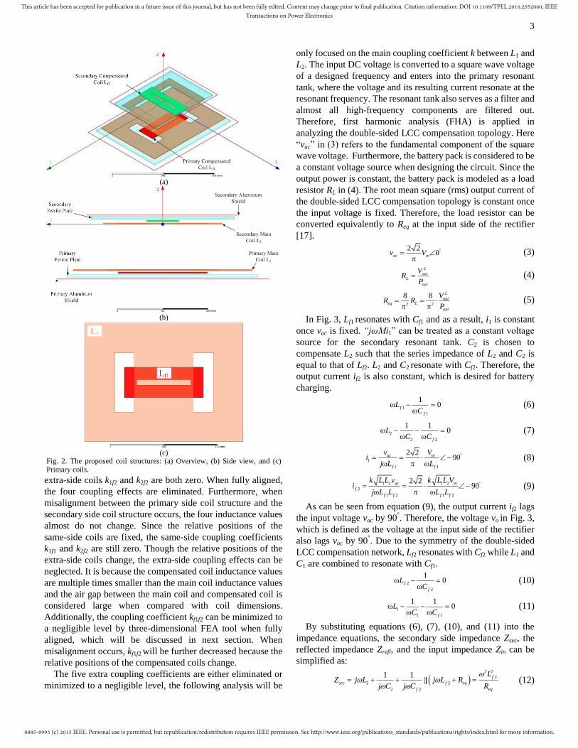
Fig. 2 presents the proposed integrated coil structure. Bipolar
coils are selected as the main coils L1 and L2 because of the
outstanding performance and good misalignment tolerance
[11]. Due to the onboard space limitation, the size of the
secondary side is smaller than that of the primary side. Unipolar
coils are chosen for compensated coils Lf1 and Lf2. Since both
the primary side and the secondary side have similar coil
structures, analysis will be first focused on one side. On the
primary side, the bipolar coil L1 performs as a magnetic dipole
and the magnetic flux excited by L1 passes through the
compensated coil Lf1. The amount of the magnetic flux can be
expressed as ψ1f1,
11 1 1 ff B d S (1)
where “B1” stands for the magnetic flux density and “Sf1”
represents the area of the primary compensated coil Lf1. The
compensated coil is placed in the center of the coil structure in a
different layer. As a main characteristic of a magnetic dipole,
the magnetic flux it excites is symmetrical in space; therefore,
the amount of the magnetic flux flows into the compensated
coil equals to that flows out of it. As a result, the net magnetic
flux passing through Lf1 is zero. Since ψ1f1 is zero, the coupling
coefficient is zero so the coupling effect is eliminated,
1 1 11
1 1
11 1 1
0f f
f
f f
k
(2)
where ψf11 is the amount of magnetic flux excited by Lf1 passes
through L1, ψ11 and ψf1f1 represent the amounts of their
self-magnetic flux. Similarly, the net amount of magnetic flux
which is excited by L2 and passes through Lf2 is zero so the
coupling coefficient k2f2 is zero. Moreover, the net amount of
magnetic flux which is excited by L1 and passes through Lf2 is
zero and the net amount of magnetic flux which is excited by L2
and passes through Lf1 is also zero. The coupling coefficients of
Fig. 1. Double-sided LCC compensation topology with compensated coils’
integration.
0885-8993 (c) 2015 IEEE. Personal use is permitted, but republication/redistribution requires IEEE permission. See http://www.ieee.org/publications_standards/publications/rights/index.html for more information.
This article has been accepted for publication in a future issue of this journal, but has not been fully edited. Content may change prior to final publication. Citation information: DOI 10.1109/TPEL.2016.2552060, IEEETransactions on Power Electronics
3
extra-side coils k1f2 and k2f2 are both zero. When fully aligned,
the four coupling effects are eliminated. Furthermore, when
misalignment between the primary side coil structure and the
secondary side coil structure occurs, the four inductance values
almost do not change. Since the relative positions of the
same-side coils are fixed, the same-side coupling coefficients
k1f1 and k2f2 are still zero. Though the relative positions of the
extra-side coils change, the extra-side coupling effects can be
neglected. It is because the compensated coil inductance values
are multiple times smaller than the main coil inductance values
and the air gap between the main coil and compensated coil is
considered large when compared with coil dimensions.
Additionally, the coupling coefficient kf1f2 can be minimized to
a negligible level by three-dimensional FEA tool when fully
aligned, which will be discussed in next section. When
misalignment occurs, kf1f2 will be further decreased because the
relative positions of the compensated coils change.
The five extra coupling coefficients are either eliminated or
minimized to a negligible level, the following analysis will be
only focused on the main coupling coefficient k between L1 and
L2. The input DC voltage is converted to a square wave voltage
of a designed frequency and enters into the primary resonant
tank, where the voltage and its resulting current resonate at the
resonant frequency. The resonant tank also serves as a filter and
almost all high-frequency components are filtered out.
Therefore, first harmonic analysis (FHA) is applied in
analyzing the double-sided LCC compensation topology. Here
“vac” in (3) refers to the fundamental component of the square
wave voltage. Furthermore, the battery pack is considered to be
a constant voltage source when designing the circuit. Since the
output power is constant, the battery pack is modeled as a load
resistor RL in (4). The root mean square (rms) output current of
the double-sided LCC compensation topology is constant once
the input voltage is fixed. Therefore, the load resistor can be
converted equivalently to Req at the input side of the rectifier
[17].
2 20ac inv V
(3)
2
outL
out
VR
P (4)
2
2 2
8 8 outeq L
out
VR R
P
(5)
In Fig. 3, Lf1 resonates with Cf1 and as a result, i1 is constant
once vac is fixed. “jωMi1” can be treated as a constant voltage
source for the secondary resonant tank. C2 is chosen to
compensate L2 such that the series impedance of L2 and C2 is
equal to that of Lf2. L2 and C2 resonate with Cf2. Therefore, the
output current if2 is also constant, which is desired for battery
charging.
1
1
10f
f
LC
(6)
2
2 2
1 10
f
LC C
(7)
1
1 1
2 290ac in
f f
v Vi
j L L
(8)
1 2 1 2
2
1 2 1 2
2 290ac in
f
f f f f
k L L v k L L Vi
j L L L L
(9)
As can be seen from equation (9), the output current if2 lags
the input voltage vac by 90°. Therefore, the voltage vo in Fig. 3,
which is defined as the voltage at the input side of the rectifier
also lags vac by 90°. Due to the symmetry of the double-sided
LCC compensation network, Lf2 resonates with Cf2 while L1 and
C1 are combined to resonate with Cf1.
2
2
10f
f
LC
(10)
1
1 1
1 10
f
LC C
(11)
By substituting equations (6), (7), (10), and (11) into the
impedance equations, the secondary side impedance Zsec, the
reflected impedance Zrefl, and the input impedance Zin can be
simplified as:
2 2
2
2 2
2 2
1 1 f
sec f eq
f eq
LZ j L j L R
j C j C R
(12)
(a)
(b)
(c)
Fig. 2. The proposed coil structures: (a) Overview, (b) Side view, and (c) Primary coils.
0885-8993 (c) 2015 IEEE. Personal use is permitted, but republication/redistribution requires IEEE permission. See http://www.ieee.org/publications_standards/publications/rights/index.html for more information.
This article has been accepted for publication in a future issue of this journal, but has not been fully edited. Content may change prior to final publication. Citation information: DOI 10.1109/TPEL.2016.2552060, IEEETransactions on Power Electronics
4
2 2
2
1
refl
sec
j i MZ
i Z
, 1 2M k L L (13)
2 2 2
1 2
1 1 2
1 1
1 1 f f
in f refl
f eq
L LZ j L j L Z
j C j C M R
(14)
where M in equation (13) represents the mutual inductance
between L1 and L2. In this lossless analysis, the input power
equals to the output power. Therefore, the expression of the
system power is given by
, 1 2
, 2
1 2
8AC RMS in out
in out AC RMS
in f f
V k L L V VP P V
Z L L
(15)
The voltage at the input side of the rectifier vo, the input
current if1, and the current in the secondary main coil i2 can be
written as
2
2 290o f eq outv i R V
(16)
1 2 1 2
1
1 2 1 2
2 20o out
f
f f f f
k L L v k L L Vi
j L L j L L
(17)
2
2 2
2 20o out
f f
v Vi
j L L
(18)
From equations (3), (9), (16), and (17), it is obvious that vac is in
phase with if1 and vo is in phase with if2. Zero phase angle (ZPA)
is achieved and no reactive power is needed from the power
source. Moreover, vac leads vo by 90° and the energy resonates
between the primary side and secondary side back and forth.
III. DESIGN PROCEDURES
1. Main Coil Simulation
Based on equation (15), the coupling coefficient k between
the main coils L1 and L2 is closely related to the power transfer
ability of a wireless power transfer system with the
double-sided LCC compensation topology. The value of k
depends on the coil geometry. Therefore, once the dimensions
of the coils are fixed, it is preferred to maximize k by changing
the coil widths in both the primary and the secondary sides.
Since the application is for passenger electric vehicles, the
space is quite limited on the vehicle. So, the receiving coil
installed on the car is better to be smaller than the transmitting
coil placed on the ground. Fig. 4(a) shows the overview of the
proposed main coil structure. We decide to choose the
dimension of the transmitting coil at the primary side as “600
mm*450 mm*4 mm” and that of the receiving coil at the
secondary side as “400 mm*300 mm*4 mm”. Ferrite plates and
aluminum shields are used for magnetic and electric shielding.
They are also made successively larger to provide the needed
shielding effects. The primary side ferrite plate has a dimension
of “640mm*496mm*8mm” while the secondary is “480
mm*352 mm*8 mm”. Aluminum shields are modelled with a
primary dimension of “711.2 mm*558.8 mm*2 mm” and a
secondary dimension of “508 mm*406 mm*2 mm”. As shown
in Fig. 4(a), there are two design variables: the primary coil
width and secondary coil width. By varying the two variables,
the coupling coefficient k can be maximized. In our case, kmax is
0.1764 with the primary coil width of 112 mm and the
secondary coil width of 48 mm. Fig. 4(b) shows the simulation
results.
2. Main Coil Winding and Measurement
Two design requirements must be met: (1) the designed
resonant frequency is 85 kHz and (2) the maximum efficiency
is achieved at the desired output power. Additionally, there are
eight components in the double-sided compensation topology.
If each component has a little variance from the designed value,
it will be hard to meet the two requirements at the same time.
Therefore, it is highly recommended to build and measure each
component right after simulation.
3. Optimization of Lf1 and Lf2 at maximum efficiency
According to equation (15), once the resonant frequency, the
system power, the main coupling coefficient, and the
inductance values of the main coils are determined, the product
of the compensated coil inductance values is fixed. A number
of combinations could contribute to the same product and it is
desired to optimize the values based on the efficiency curve of
the system. The system is required to achieve the highest
efficiency at the desired output power and the compensated
(a)
(b)
Fig. 4. (a) Overview of the main coil structure and (b) Coupling coefficient k
with different coil widths.
Fig. 3. Resonant circuits with double-sided LCC compensation topology
0885-8993 (c) 2015 IEEE. Personal use is permitted, but republication/redistribution requires IEEE permission. See http://www.ieee.org/publications_standards/publications/rights/index.html for more information.
This article has been accepted for publication in a future issue of this journal, but has not been fully edited. Content may change prior to final publication. Citation information: DOI 10.1109/TPEL.2016.2552060, IEEETransactions on Power Electronics
5
inductance values can be optimized at that point. Once the
output power is fixed, the system efficiency is determined by
the power loss, which is closely related to the equivalent series
resistance (ESR) of each component. The ESRs of the inductors
can be calculated by their quality factors and inductance values
and the ESRs of the capacitors rest with their dissipation
factors. We can write expressions for the ESRs as
11
1
LR
Q
, 2
2
2
LR
Q
, 1
1
1
f
f
f
LR
Q
, 2
2
2
f
f
f
LR
Q
(19)
1
1
1CR DF
j C
, 2
2
1CR DF
j C
,
1
1
1Cf
f
R DFj C
,
2
2
1Cf
f
R DFj C
(20)
where Q1, Q2, Qf1, and Qf2 stand for the quality factors of L1, L2,
Lf1, and Lf2 respectively.Q1 and Q2 can be measured by LCR
meters since they have already been built in the last step. Qf1
and Qf2 can be approximated at 200 based on their inductance
values, which are multiple times smaller than the main coil
inductance values. DF is the dissipation factor of the capacitors.
Once the compensated inductance values are given, the
capacitance values can be calculated by equations (6), (7), (10),
and (11). In this paper, 5PT series polypropylene and foil
resonant power supply capacitors from Electronic Concepts are
used and its DF is claimed to be 0.05%.
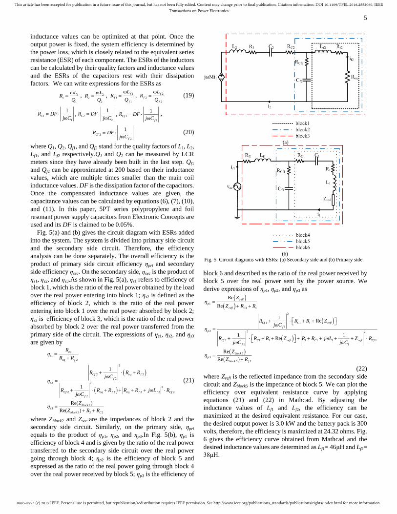
Fig. 5(a) and (b) gives the circuit diagram with ESRs added
into the system. The system is divided into primary side circuit
and the secondary side circuit. Therefore, the efficiency
analysis can be done separately. The overall efficiency is the
product of primary side circuit efficiency ηpri and secondary
side efficiency ηsec. On the secondary side, ηsec is the product of
ηs1, ηs2, and ηs3.As shown in Fig. 5(a), ηs1 refers to efficiency of
block 1, which is the ratio of the real power obtained by the load
over the real power entering into block 1; ηs2 is defined as the
efficiency of block 2, which is the ratio of the real power
entering into block 1 over the real power absorbed by block 2;
ηs3 is efficiency of block 3, which is the ratio of the real power
absorbed by block 2 over the real power transferred from the
primary side of the circuit. The expressions of ηs1, ηs2, and ηs3
are given by
1
2
2
2 2
2
2 2
2
2 2 2 2 2
2
23
2 2 2
1
1
Re( )
Re( )
eq
s
eq f
Cf eq f
f
s
Cf eq f eq f f Cf
f
blocks
block C
R
R R
R R Rj C
R R R R R j L Rj C
Z
Z R R
(21)
where Zblock2 and Zsec are the impedances of block 2 and the
secondary side circuit. Similarly, on the primary side, ηpri
equals to the product of ηp1, ηp2, and ηp3.In Fig. 5(b), ηp1 is
efficiency of block 4 and is given by the ratio of the real power
transferred to the secondary side circuit over the real power
going through block 4; ηp2 is the efficiency of block 5 and
expressed as the ratio of the real power going through block 4
over the real power received by block 5; ηp3 is the efficiency of
block 6 and described as the ratio of the real power received by
block 5 over the real power sent by the power source. We
derive expressions of ηp1, ηp2, and ηp3 as
1
1 1
2
1 1 1
1
2 2 2
1 1 1 1 1 1 1
1 1
5
3
5 1
Re
Re
1Re
1 1Re
Re
Re
refl
p
refl C
Cf C refl
f
p
Cf C refl C refl Cf
f
block
p
block f
Z
Z R R
R R R Zj C
R R R Z R R j L Z Rj C j C
Z
Z R
(22)
where Zrefl is the reflected impedance from the secondary side
circuit and Zblock5 is the impedance of block 5. We can plot the
efficiency over equivalent resistance curve by applying
equations (21) and (22) in Mathcad. By adjusting the
inductance values of Lf1 and Lf2, the efficiency can be
maximized at the desired equivalent resistance. For our case,
the desired output power is 3.0 kW and the battery pack is 300
volts, therefore, the efficiency is maximized at 24.32 ohms. Fig.
6 gives the efficiency curve obtained from Mathcad and the
desired inductance values are determined as Lf1= 46μH and Lf2=
38μH.
(a)
(b)
Fig. 5. Circuit diagrams with ESRs: (a) Secondary side and (b) Primary side.

0885-8993 (c) 2015 IEEE. Personal use is permitted, but republication/redistribution requires IEEE permission. See http://www.ieee.org/publications_standards/publications/rights/index.html for more information.
This article has been accepted for publication in a future issue of this journal, but has not been fully edited. Content may change prior to final publication. Citation information: DOI 10.1109/TPEL.2016.2552060, IEEETransactions on Power Electronics
6
4. Maxwell Simulation for Lf1 and Lf2
As analyzed in the previous section, a unipolar compensated
coil is preferred in a coil structure with bipolar main coils. In
order to further decrease the coupling effects between the main
coil and the compensated coil, it is more desired to place the
compensated coil in the region with weaker magnetic field
densities. By substituting Lf1 and Lf2 into (8) and (18), the
currents flowing through L1 and L2 can be determined and set as
the excitation currents in the Maxwell model. Vacuum boxes
are built up at the expected positions of the compensated coils,
which are shown in Fig. 7(a). Fig. 7(b) gives the simulation
results of magnetic flux densities in the vacuum boxes.
Clearly, the magnetic field is weaker in the central areas of
the two main coils, which are circled by the dashed lines in Fig.
7(b). The compensated coils should be placed in those areas.
With the desired inductance values, the compensated coils are
built and simulated in ANSYS MAXWELL.
The compensated coils with the desired values are placed in
the system as shown in Fig. 8(a) and the coupling coefficient
kf1f2 is 0.05, which is good enough for the experiment.
However, it can be further optimized. Since Fig. 7(b) indicates
a larger area with weaker magnetic flux density on the primary
side, so the primary compensated coil has enough area to be
placed. By rotating the primary compensated coil from 0° to
180° as shown in Fig. 8(b), the lowest coupling case is achieved.
Fig. 9(a) shows the coupling coefficient kf1f2 of the
compensated coils and the same-side coupling coefficients k1f1
and k2f2. It is obvious that kf1f2 is minimized as 0.04 at 90°
rotating angle while the same-side coupling coefficients are
almost equal to zero with the angle rotating. Fig. 9(b)
demonstrates that the self-inductance values of the two
compensated coils keep almost constant with the angle rotating.
5. Compensated Coil Winding and Measurement
With the parameters provided by MAXWELL simulation,
compensated coils are wound and measured. Again, in order to
make the resonate frequency at 85 kHz and the efficiency
maximized at the desired output power, capacitance values
need to be recalculated with the measured results of L1, L2, Lf1,
and Lf2 through equations (6), (7), (10), and (11). The
capacitance values calculated in this step only slightly vary
from those calculated in step 3. Therefore, the efficiency will
not be affected.
Fig. 6. Efficiency over equivalent resistance curve.
(a)
(b)
Fig. 7. (a) Side view of the coil structure with vacuum boxes and (b) Magnetic
field densities of the vacuum boxes
(a)
(b)
Fig. 8. (a) Coil structure with compensated coil integrated into the system and (b) Rotating the primary compensated coil.
0885-8993 (c) 2015 IEEE. Personal use is permitted, but republication/redistribution requires IEEE permission. See http://www.ieee.org/publications_standards/publications/rights/index.html for more information.
This article has been accepted for publication in a future issue of this journal, but has not been fully edited. Content may change prior to final publication. Citation information: DOI 10.1109/TPEL.2016.2552060, IEEETransactions on Power Electronics
7
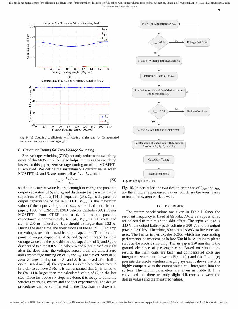
6. Capacitor Tuning for Zero Voltage Switching
Zero voltage switching (ZVS) not only reduces the switching
noise of the MOSFETs, but also helps minimize the switching
losses. In this paper, zero voltage turning on of the MOSFETs
is achieved. We define the instantaneous current value when
MOSFETs S1 and S4 are turned off as IOFF. IOFF must
,2 OSS in max
OFF
dead
C VI
t (23)
so that the current value is large enough to charge the parasitic
output capacitors of S1 and S4 and discharge the parasitic output
capacitors of S2 and S3 [14]. In equation (23), Coss is the parasitic
output capacitance of the MOSFET, Vin,max is the maximum
value of the input voltage, and tdead is the dead time. In this
paper, 1200 V C2M0025120D Silicon Carbide (SiC) Power
MOSFETs from CREE are used. Its output parasitic
capacitance is approximately 400 pF, Vin,max is 330 volts, and
tdead is 200 ns. Therefore, IOFF should be larger than 1.32 A.
During the dead time, the body diodes of the MOSFETs clamp
the voltages over the parasitic output capacitors. Therefore, the
parasitic output capacitors of S1 and S4 are charged to input
voltage value and the parasitic output capacitors of S2 and S3 are
discharged to almost 0 V. So, when S2 and S3 are turned on right
after the dead time, the voltages across them are almost zero
and zero voltage turning on of S2 and S3 is achieved. Similarly,
zero voltage turning on of S1 and S4 is achieved after half a
cycle. Based on [14], the capacitor C2 is the best choice to tune
in order to achieve ZVS. It is demonstrated that C2 is tuned to
be 8%~11% larger than the calculated value of C2 in the last
step. Once the above six steps are done, it is ready to build the
wireless charging system and conduct experiments. The design
procedures can be summarized in the flowchart as shown in
Fig. 10. In particular, the two design criterions of kmax and kf1f2
are the authors’ experienced values, which are the worst cases
to make the system work as well.
IV. EXPERIMENT
The system specifications are given in Table I. Since the
resonant frequency is fixed at 85 kHz, AWG-38 copper wires
are selected to minimize the skin effect. The input voltage is
330 V, the output battery pack voltage is 300 V, and the output
power is 3.0 kW. Therefore, 800-strand AWG-38 litz wires are
used. The ferrite is Ferroxcube 3C95, which has outstanding
performance at frequencies below 500 kHz. Aluminum plates
serve as the electric shielding. The air gap is 150 mm due to the
ground clearance of passenger cars. Based on simulations
results, the main coils are built and compensated coils are
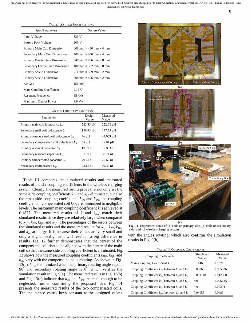
integrated, which are shown in Fig. 11(a) and (b). Fig. 11(c)
presents the whole wireless charging system. It shows that it is
highly compact with the compensated coil integrated into the
system. The circuit parameters are given in Table II. It is
convinced that there are only slight differences between the
design values and the measured values.
(a)
(b)
Fig. 9. (a) Coupling coefficients with rotating angles and (b) Compensated
inductance values with rotating angles.
kmax > 0.14
Main Coil Simulation for kmax
L1 and L2 Winding and Measurement
Enlarge Coil Size
Determine Lf1 and Lf2 at ηmax
Simulation for Lf1 and Lf2 of desired values
and to minimize kf1f2
Reduce Coil Sizekf1f2 < 0.08
Lf1 and Lf2 Winding and Measurement
Capacitors Tuning
Experiment Setup
Yes
Yes
No
No
Recalculation of Capacitors with Measured
Results of L1, L2, Lf1, and Lf2
Fig. 10. Design flowchart.
0885-8993 (c) 2015 IEEE. Personal use is permitted, but republication/redistribution requires IEEE permission. See http://www.ieee.org/publications_standards/publications/rights/index.html for more information.
This article has been accepted for publication in a future issue of this journal, but has not been fully edited. Content may change prior to final publication. Citation information: DOI 10.1109/TPEL.2016.2552060, IEEETransactions on Power Electronics
8
Table III compares the simulated results and measured
results of the six coupling coefficients in the wireless charging
system. Clearly, the measured results prove that not only are the
same-side coupling coefficients k1f1 and k2f2 eliminated, but also
the cross-side coupling coefficients k1f2 and k2f1, the coupling
coefficient of compensated coil kf1f2 are minimized to negligible
levels. The maximum main coupling coefficient k is achieved at
0.1877. The measured results of k and kf1f2 match their
simulated results since they are relatively large when compared
to k1f1, k2f2, k1f2, and k2f1. The percentages of the errors between
the simulated results and the measured results for k1f1, k2f2, k1f2,
and k2f1 are large. It is because their values are very small and
only a slight misalignment will result in a big difference in
results. Fig. 12 further demonstrates that the center of the
compensated coil should be aligned with the center of the main
coil so that the same-side coupling coefficient is eliminated. Fig.
13 shows how the measured coupling coefficients kf1f2, k1f1, and
k2f2 vary with the compensated coils rotating. As shown in Fig.
13(a), kf1f2 is minimized when the primary rotating angle equals
90° and secondary rotating angle is 0°, which verifies the
simulation result in Fig. 9(a). The measured results in Fig. 13(b)
and Fig. 13(c) indicate that k1f1 and k2f2 are small enough to be
neglected, further confirming the proposed idea. Fig. 14
presents the measured results of the two compensated coils.
The inductance values keep constant at the designed values
with the angles rotating, which also confirms the simulation
results in Fig. 9(b).
TABLE I .SYSTEM SPECIFICATIONS
Spec/Parameters Design Value
Input Voltage 330 V
Battery Pack Voltage 300 V
Primary Main Coil Dimension 600 mm × 450 mm × 4 mm
Secondary Main Coil Dimension 400 mm × 300 mm × 4 mm
Primary Ferrite Plate Dimension 640 mm × 496 mm × 8 mm
Secondary Ferrite Plate Dimension 480 mm × 352 mm × 8 mm
Primary Shield Dimension 711 mm × 559 mm × 2 mm
Primary Shield Dimension 508 mm × 406 mm × 2 mm
Air Gap 150 mm
Main Coupling Coefficient 0.1877
Resonant Frequency 85 kHz
Maximum Output Power 3.0 kW
TABLE II. CIRCUIT PARAMETERS
Parameters Design
Value
Measured
Value
Primary main coil inductance L1 225.35 μH 222.98 μH
Secondary mail coil inductance L2 159.45 μH 157.55 μH
Primary compensated coil inductance Lf1 46 μH 44.059 μH
Secondary compensated coil inductance Lf2 38 μH 38.04 μH
Primary resonant capacitor C1 19.59 nF 19.853 nF
Secondary resonant capacitor C2 31.39 nF 32.71 nF
Primary compensated capacitor Cf1 79.68 nF 79.69 nF
Secondary compensated Cf2 92.16 nF 92.36 nF
(a)
(b)
(c)
Fig. 11. Experiment setup of (a) coils on primary side, (b) coils on secondary side, and (c) wireless charging system
TABLE III. COUPLING COEFFICIENTS
Coupling Coefficients Simulated
Value
Measured
Value
Main Coupling Coefficient k 0.1746 0.1877
Coupling Coefficient k1f1 between L1 and Lf1 0.00068 0.005826
Coupling Coefficient k2f2 between L2 and Lf2 0.001118 0.012368
Coupling Coefficient k1f2 between L1 and Lf2 ≈ 0 0.006135
Coupling Coefficient k2f1 between L2 and Lf1 ≈ 0 0.002941
Coupling Coefficient kf1f2 between Lf1 and Lf2 0.04053 0.0483

0885-8993 (c) 2015 IEEE. Personal use is permitted, but republication/redistribution requires IEEE permission. See http://www.ieee.org/publications_standards/publications/rights/index.html for more information.
This article has been accepted for publication in a future issue of this journal, but has not been fully edited. Content may change prior to final publication. Citation information: DOI 10.1109/TPEL.2016.2552060, IEEETransactions on Power Electronics
9
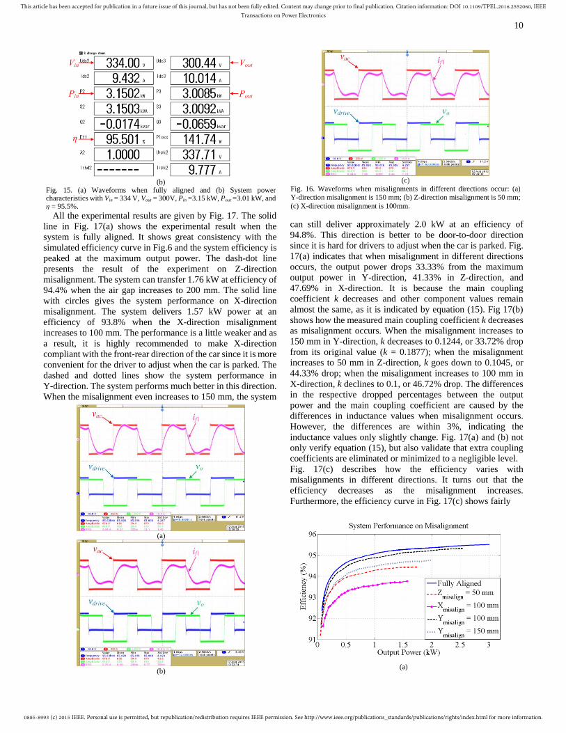
Fig. 15(a) represents the waveforms of the primary resonant
tank’s input voltage vac and input current if1, the secondary
resonant tank’s output voltage vo, and MOSFET gate-to-source
voltage Vdrive. In this paper, the purpose of observing Vdrive is to
ensure that the gate-to-source voltage is in its maximum rating
all the time since noises may appear during the experiment.
Here, vac leads if1 by 13.4° and the turn-off current IOFF is
approximately 4.5 A, which is much larger than 1.32 A and
sufficient for charging and discharging the parasitic output
capacitors. Fig. 15(b) gives power characteristics of the
wireless charging system at the maximum output power. When
fully aligned, the system is able to deliver 3.0 kW output power
at DC-DC efficiency as high as 95.5%. Further experiments on
misalignments are also conducted in the Y-direction,
X-direction, and Z-direction separately. Fig. 16(a) to (c) give
the respective waveforms. Since the input voltage and the
battery pack voltage are fixed at 330 V and 300 V, the
waveforms of vac and vo remain the same. However, the
waveform of if1 gradually deviates from its original waveform
shown in Fig. 15(a). When misalignments in different
directions occur, the main coupling coefficient k decreases and
the output power goes down, as indicated by equation (15).
Therefore, the rms value of if1 becomes smaller. Moreover, the
mutual inductance M between the main coils decreases and as a
result, both the reflected impedance Zrefl and input impedance
Zin change. The input phase angle between vac and if1 increases,
which causes the turn-off current IOFF to increase and the
high-order harmonics components in if1 to rise. The decreased
rms value of if1, the increased turn-off current value and
high-order harmonics components in if1 result in the waveform
distortions when misalignments occur. Fig. 16(a) shows the
waveforms when Y-direction misalignment is 150 mm. Since k
and M are still comparable to their original values when fully
aligned, the waveform distortion of if1 is low. However, when k
and M further decreases, the waveform distortion turns high, as
shown in Fig. 16(b) and (c). Here, Z-direction misalignment is
50 mm means air gap is increased from 150 mm to 200 mm.
Fig. 12. Horizontal misalignment effects on k1f1.
(a)
(b)
(c)
Fig. 13 Coupling coefficients (a) kf1f2, (b) k1f1, and (c) k2f2 with compensated
coils rotating.
(a)
(b)
Fig. 14. Compensated inductances values (a) Lf1 and (b) Lf2 with the compensated coils rotating.
(a)
0885-8993 (c) 2015 IEEE. Personal use is permitted, but republication/redistribution requires IEEE permission. See http://www.ieee.org/publications_standards/publications/rights/index.html for more information.
This article has been accepted for publication in a future issue of this journal, but has not been fully edited. Content may change prior to final publication. Citation information: DOI 10.1109/TPEL.2016.2552060, IEEETransactions on Power Electronics
10
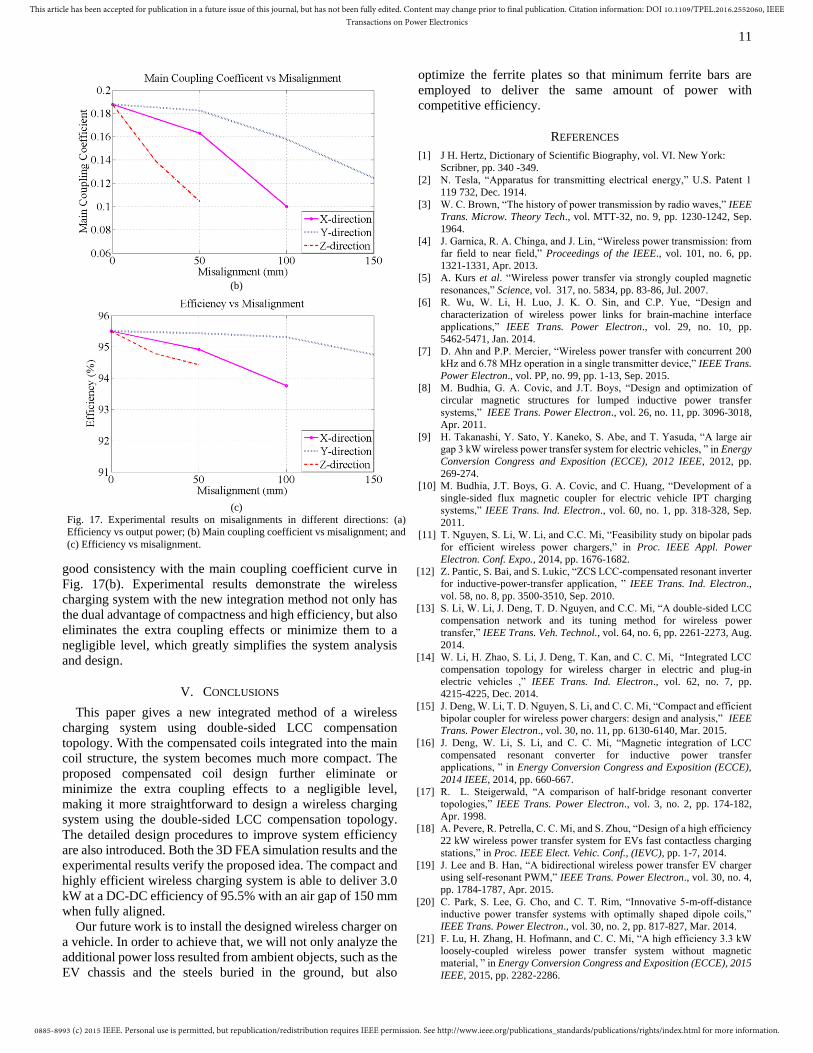
All the experimental results are given by Fig. 17. The solid
line in Fig. 17(a) shows the experimental result when the
system is fully aligned. It shows great consistency with the
simulated efficiency curve in Fig.6 and the system efficiency is
peaked at the maximum output power. The dash-dot line
presents the result of the experiment on Z-direction
misalignment. The system can transfer 1.76 kW at efficiency of
94.4% when the air gap increases to 200 mm. The solid line
with circles gives the system performance on X-direction
misalignment. The system delivers 1.57 kW power at an
efficiency of 93.8% when the X-direction misalignment
increases to 100 mm. The performance is a little weaker and as
a result, it is highly recommended to make X-direction
compliant with the front-rear direction of the car since it is more
convenient for the driver to adjust when the car is parked. The
dashed and dotted lines show the system performance in
Y-direction. The system performs much better in this direction.
When the misalignment even increases to 150 mm, the system
can still deliver approximately 2.0 kW at an efficiency of
94.8%. This direction is better to be door-to-door direction
since it is hard for drivers to adjust when the car is parked. Fig.
17(a) indicates that when misalignment in different directions
occurs, the output power drops 33.33% from the maximum
output power in Y-direction, 41.33% in Z-direction, and
47.69% in X-direction. It is because the main coupling
coefficient k decreases and other component values remain
almost the same, as it is indicated by equation (15). Fig 17(b)
shows how the measured main coupling coefficient k decreases
as misalignment occurs. When the misalignment increases to
150 mm in Y-direction, k decreases to 0.1244, or 33.72% drop
from its original value (k = 0.1877); when the misalignment
increases to 50 mm in Z-direction, k goes down to 0.1045, or
44.33% drop; when the misalignment increases to 100 mm in
X-direction, k declines to 0.1, or 46.72% drop. The differences
in the respective dropped percentages between the output
power and the main coupling coefficient are caused by the
differences in inductance values when misalignment occurs.
However, the differences are within 3%, indicating the
inductance values only slightly change. Fig. 17(a) and (b) not
only verify equation (15), but also validate that extra coupling
coefficients are eliminated or minimized to a negligible level.
Fig. 17(c) describes how the efficiency varies with
misalignments in different directions. It turns out that the
efficiency decreases as the misalignment increases.
Furthermore, the efficiency curve in Fig. 17(c) shows fairly
(b)
Fig. 15. (a) Waveforms when fully aligned and (b) System power characteristics with Vin = 334 V, Vout = 300V, Pin =3.15 kW, Pout =3.01 kW, and η = 95.5%.
(a)
(b)
(c)
Fig. 16. Waveforms when misalignments in different directions occur: (a)
Y-direction misalignment is 150 mm; (b) Z-direction misalignment is 50 mm;
(c) X-direction misalignment is 100mm.
(a)
0885-8993 (c) 2015 IEEE. Personal use is permitted, but republication/redistribution requires IEEE permission. See http://www.ieee.org/publications_standards/publications/rights/index.html for more information.
This article has been accepted for publication in a future issue of this journal, but has not been fully edited. Content may change prior to final publication. Citation information: DOI 10.1109/TPEL.2016.2552060, IEEETransactions on Power Electronics
11
good consistency with the main coupling coefficient curve in
Fig. 17(b). Experimental results demonstrate the wireless
charging system with the new integration method not only has
the dual advantage of compactness and high efficiency, but also
eliminates the extra coupling effects or minimize them to a
negligible level, which greatly simplifies the system analysis
and design.
V. CONCLUSIONS
This paper gives a new integrated method of a wireless
charging system using double-sided LCC compensation
topology. With the compensated coils integrated into the main
coil structure, the system becomes much more compact. The
proposed compensated coil design further eliminate or
minimize the extra coupling effects to a negligible level,
making it more straightforward to design a wireless charging
system using the double-sided LCC compensation topology.
The detailed design procedures to improve system efficiency
are also introduced. Both the 3D FEA simulation results and the
experimental results verify the proposed idea. The compact and
highly efficient wireless charging system is able to deliver 3.0
kW at a DC-DC efficiency of 95.5% with an air gap of 150 mm
when fully aligned.
Our future work is to install the designed wireless charger on
a vehicle. In order to achieve that, we will not only analyze the
additional power loss resulted from ambient objects, such as the
EV chassis and the steels buried in the ground, but also
optimize the ferrite plates so that minimum ferrite bars are
employed to deliver the same amount of power with
competitive efficiency.
REFERENCES
[1] J H. Hertz, Dictionary of Scientific Biography, vol. VI. New York:
Scribner, pp. 340 -349.
[2] N. Tesla, “Apparatus for transmitting electrical energy,” U.S. Patent 1
119 732, Dec. 1914.
[3] W. C. Brown, “The history of power transmission by radio waves,” IEEE
Trans. Microw. Theory Tech., vol. MTT-32, no. 9, pp. 1230-1242, Sep.
1964.
[4] J. Garnica, R. A. Chinga, and J. Lin, “Wireless power transmission: from
far field to near field,” Proceedings of the IEEE., vol. 101, no. 6, pp.
1321-1331, Apr. 2013.
[5] A. Kurs et al. “Wireless power transfer via strongly coupled magnetic
resonances,” Science, vol. 317, no. 5834, pp. 83-86, Jul. 2007.
[6] R. Wu, W. Li, H. Luo, J. K. O. Sin, and C.P. Yue, “Design and
characterization of wireless power links for brain-machine interface
applications,” IEEE Trans. Power Electron., vol. 29, no. 10, pp.
5462-5471, Jan. 2014.
[7] D. Ahn and P.P. Mercier, “Wireless power transfer with concurrent 200
kHz and 6.78 MHz operation in a single transmitter device,” IEEE Trans.
Power Electron., vol. PP, no. 99, pp. 1-13, Sep. 2015.
[8] M. Budhia, G. A. Covic, and J.T. Boys, “Design and optimization of
circular magnetic structures for lumped inductive power transfer
systems,” IEEE Trans. Power Electron., vol. 26, no. 11, pp. 3096-3018,
Apr. 2011.
[9] H. Takanashi, Y. Sato, Y. Kaneko, S. Abe, and T. Yasuda, “A large air
gap 3 kW wireless power transfer system for electric vehicles, ” in Energy
Conversion Congress and Exposition (ECCE), 2012 IEEE, 2012, pp.
269-274.
[10] M. Budhia, J.T. Boys, G. A. Covic, and C. Huang, “Development of a
single-sided flux magnetic coupler for electric vehicle IPT charging
systems,” IEEE Trans. Ind. Electron., vol. 60, no. 1, pp. 318-328, Sep.
2011.
[11] T. Nguyen, S. Li, W. Li, and C.C. Mi, “Feasibility study on bipolar pads
for efficient wireless power chargers,” in Proc. IEEE Appl. Power
Electron. Conf. Expo., 2014, pp. 1676-1682.
[12] Z. Pantic, S. Bai, and S. Lukic, “ZCS LCC-compensated resonant inverter
for inductive-power-transfer application, ” IEEE Trans. Ind. Electron.,
vol. 58, no. 8, pp. 3500-3510, Sep. 2010.
[13] S. Li, W. Li, J. Deng, T. D. Nguyen, and C.C. Mi, “A double-sided LCC
compensation network and its tuning method for wireless power
transfer,” IEEE Trans. Veh. Technol., vol. 64, no. 6, pp. 2261-2273, Aug.
2014.
[14] W. Li, H. Zhao, S. Li, J. Deng, T. Kan, and C. C. Mi, “Integrated LCC
compensation topology for wireless charger in electric and plug-in
electric vehicles ,” IEEE Trans. Ind. Electron., vol. 62, no. 7, pp.
4215-4225, Dec. 2014.
[15] J. Deng, W. Li, T. D. Nguyen, S. Li, and C. C. Mi, “Compact and efficient
bipolar coupler for wireless power chargers: design and analysis,” IEEE
Trans. Power Electron., vol. 30, no. 11, pp. 6130-6140, Mar. 2015.
[16] J. Deng, W. Li, S. Li, and C. C. Mi, “Magnetic integration of LCC
compensated resonant converter for inductive power transfer
applications, ” in Energy Conversion Congress and Exposition (ECCE),
2014 IEEE, 2014, pp. 660-667.
[17] R. L. Steigerwald, “A comparison of half-bridge resonant converter
topologies,” IEEE Trans. Power Electron., vol. 3, no. 2, pp. 174-182,
Apr. 1998.
[18] A. Pevere, R. Petrella, C. C. Mi, and S. Zhou, “Design of a high efficiency
22 kW wireless power transfer system for EVs fast contactless charging
stations,” in Proc. IEEE Elect. Vehic. Conf., (IEVC), pp. 1-7, 2014.
[19] J. Lee and B. Han, “A bidirectional wireless power transfer EV charger
using self-resonant PWM,” IEEE Trans. Power Electron., vol. 30, no. 4,
pp. 1784-1787, Apr. 2015.
[20] C. Park, S. Lee, G. Cho, and C. T. Rim, “Innovative 5-m-off-distance
inductive power transfer systems with optimally shaped dipole coils,”
IEEE Trans. Power Electron., vol. 30, no. 2, pp. 817-827, Mar. 2014.
[21] F. Lu, H. Zhang, H. Hofmann, and C. C. Mi, “A high efficiency 3.3 kW
loosely-coupled wireless power transfer system without magnetic
material, ” in Energy Conversion Congress and Exposition (ECCE), 2015
IEEE, 2015, pp. 2282-2286.
(b)
(c)
Fig. 17. Experimental results on misalignments in different directions: (a)
Efficiency vs output power; (b) Main coupling coefficient vs misalignment; and
(c) Efficiency vs misalignment.

0885-8993 (c) 2015 IEEE. Personal use is permitted, but republication/redistribution requires IEEE permission. See http://www.ieee.org/publications_standards/publications/rights/index.html for more information.
This article has been accepted for publication in a future issue of this journal, but has not been fully edited. Content may change prior to final publication. Citation information: DOI 10.1109/TPEL.2016.2552060, IEEETransactions on Power Electronics
12
[22] A. Kamineni, G.A. Covic, and J. T. Boys, “Analysis of coplanar
intermediate coil structures in inductive power transfer systems,” IEEE
Trans. Power Electron., vol. 30, no. 11, pp. 6141-6154, Nov. 2015.
[23] W. Zhang and C. C. Mi, “Compensation topologies for high power
wireless power transfer systems,” IEEE Trans. Veh. Technol., vol. PP, no.
99, pp. 1-10, Jul. 2015 Tianze Kan (S’15) received the B.Eng. degree in
electrical engineering and automation from
Huazhong University of Science and Technology
(HUST), Wuhan, China, in 2011 and the M.S. degree
in electrical engineering from the University of
Southern California (USC), Los Angeles, CA, USA,
in 2013. He is currently working on his Ph.D. degree
in electrical and computer engineering in the joint
doctoral program between San Diego State
University (SDSU) and the University of California at
San Diego (UCSD), La Jolla, CA, USA.
His research interests include inductive based wireless power transfer,
especially on coil design and compensation topologies.
Trong Duy Nguyen was born in Binh Dinh,
Vietnam. He received his B.Eng. and M.Eng. from
the Hochiminh-City University of Technology,
Vietnam, in 2004 and 2007, and his Ph.D. from the
Nanyang Technological University, Singapore, in
2012. His current research interests include electrical
machine design and drives, electromagnetics, and
electrical energy conversion systems.
Jeff C. White received Associates Degree in Motive
Power Technology St Clair College, Windsor, Ontario
in 1981. First R&D position was with CNG Systems
in Livonia, MI, USA, for development of Compressed
Natural Gas Dual Fuel systems for light vehicles in
1986 and a supervisor at AMC /Chrysler Aero
Dynamics laboratories in 1988.
While at DENSO International America, Inc. since
1988, he was responsible for management of vehicle
and component testing of fuel systems, thermal
systems and NVH areas. Major achievements were,
Denso to GM, Ford, Chrysler wind tunnel correlation and ISO QS 9000 lead
auditor. As a Senior Manager he became responsible for of all testing facilities
including overseeing testing facility designs and implementation including ISO
17025 Laboratory Accreditation and GM, Ford, Chrysler AEMCLRP
certification for Emissions Radiated and Conducted Testing. Key initial
research areas were alternative fuels with focus on NH3 from Wind power. He
is currently overseeing collaborative academic projects related to vehicle
electrification such as, in wheel motors and wireless charging. Keen interests
are simulation modelling to experimental validations as related to Human
safety.
Rajesh K. Malhan received the M.Sc. (Electronics),
M.Phil., and Ph.D. degrees from the University of
Delhi, India in 1982, 1984 and 1989, respectively. He
was post-doctoral research fellow in the Department
of Electrical and Electronic Engineering (Electron
Device Group), Toyohashi University of Technology,
Japan till March 1991. He joined DENSO
Corporation (formerly Nippondenso Co., Ltd.) same
year, where he was responsible for III-V compound
semiconductor electrical and optical device R&D at
DENSO headquarter, Kariya. In 1996, he started working in DENSO Research
Laboratories, where he played the major role in established a major research
program in the field of wide band gap semiconductor Silicon Carbide (SiC)
power electronics (power device & modules). He is director of advanced
research at DENSO’s North American Research and Development Department.
He is responsible for DENSO’s Automotive (Autonomous drive, Vehicle
electrification, Vehicle wireless charging, Alternative fuel and Metal air battery
technologies) R&D work. He has published more than 50 research journal
papers, inventor or co-inventor on over 25 US and 150 International patents,
and contributed chapters in 4 books. He is a winner of 24th JSAP (Japan
Society of Applied Physics) year 2002 award for outstanding achievements in
the field of applied physics. He is a member of the Society of Automotive
Engineers (USA), the Institute of Electrical and Electronics Engineers, Inc.
(USA), the Japan Society of Applied Physics (Japan) and served on many
international professional society committees.
Chunting Chris Mi (S’00–A’01–M’01–SM’03–
F’12) received the B.S.E.E. and M.S.E.E. degrees in
electrical engineering from Northwestern
Polytechnical University, Xi’an, China, in 1985 and
1988, and the Ph.D. degree in electrical engineering
from the University of Toronto, Toronto, Ontario,
Canada, in 2001. He is a Professor and chair of
electrical and computer engineering and the Director
of the Department of Energy (DOE) -funded
Graduate Automotive Technology Education
(GATE) Center for Electric Drive Transportation,
San Diego State University, San Diego, USA. Prior to joining SDSU, he was
with with University of Michigan, Dearborn from 2001 to 2015. He was the
President and the Chief Technical Officer of 1Power Solutions, Inc. from 2008
to 2011. He is the Co-Founder of Gannon Motors and Controls LLC and Mia
Motors, Inc.
His research interests include electric drives, power electronics, electric
machines, renewable-energy systems, and electrical and hybrid vehicles. He
has conducted extensive research and has published more than 100 journal
papers. He has taught tutorials and seminars on the subject of HEVs/PHEVs for
the Society of Automotive Engineers (SAE), the IEEE, workshops sponsored
by the National Science Foundation (NSF), and the National Society of
Professional Engineers. He has delivered courses to major automotive OEMs
and suppliers, including GM, Ford, Chrysler, Honda, Hyundai, Tyco
Electronics, A&D Technology, Johnson Controls, Quantum Technology,
Delphi, and the European Ph.D School. He has offered tutorials in many
countries, including the U.S., China, Korea, Singapore, Italy, France, and
Mexico. He has published more than 100 articles and delivered 30 invited talks
and keynote speeches. He has also served as a panelist in major IEEE and SAE
conferences.
Dr. Mi is the recipient of “Distinguished Teaching Award” and
“Distinguished Research Award” of University of Michigan Dearborn. He is a
recipient of the 2007 IEEE Region 4 “Outstanding Engineer Award,” “IEEE
Southeastern Michigan Section Outstanding Professional Award.” and the
“SAE Environmental Excellence in Transportation (E2T).