a new failure mechanism on analog i/ o cell under nd-mode
TRANSCRIPT

0-7803-9301-5/05/$20.00 ©2005 IEEE 209 Proceedings of 12th IPFA 2005, Singapore
A New Failure Mechanism on Analog I/O Cell under ND-Mode ESD Stress in Deep-Submicron CMOS Technology
Shih-Hung Chen1, Ming-Dou Ker2, and Che-Hao Chuang1
1ESD & Product Engineering Department, System-on-Chip Technology Center Industrial Technology Research Institute, Taiwan.
2Nanoelectronics and Gigascale Systems Laboratory, Institute of Electronics National Chiao-Tung University, Taiwan.
Phone: 886-3-5917017 Fax: 886-3-5912060 Email: [email protected]
Abstract A new ESD failure mechanism has been found in the
analog pins with pure-diode protection scheme during ND-mode ESD stress. The failure is caused by the parasitic npn interaction between ESD protection diode and guard ring structure. The parasitic npn bipolar, which was constructed between the N+/PW diode and the N+/NW guard ring, provides the discharging path between the I/O pad to the grounded VDD under the ND-mode ESD stress to cause a low ESD robustness of the analog I/O cell. The solution to overcome this ESD failure is also proposed.
1. Introduction In deep-submicron CMOS technology, electrostatic
discharge (ESD) protection has been an important concern on the reliability of IC products [1]-[3]. Due to the low breakdown voltage of the thinner gate oxide, an efficient ESD protection circuit must be designed to clamp the overstress voltage across the gate oxide of the internal circuits. A conventional ESD protection design for the digital input pin is shown in Fig. 1. The gate-grounded NMOS (GGNMOS) and the gate-VDD PMOS (GDPMOS) devices are often designed with large device dimension and wider drain-contact-to-poly-gate layout spacing to sustain the requested ESD level [4], [5]. The resistor R of the digital input ESD protection circuit is usually installed to protect the gate oxide of input stage. However, the series resistance between the input pad and input stage is forbidden for current-mode input signals or high-frequency applications. Furthermore, the series resistance and the large junction capacitance of the ESD clamp devices cause a long RC delay to the input signals, therefore such ESD protection circuit is not suitable for analog pins [6].
The basic ESD protection scheme for analog I/O pin is shown in Fig. 2 [6]. In order to reduce the input capacitance of the analog pin for high-frequency applications, the N-cell and P-cell are both designed with much smaller device dimensions. However, such small devices can’t sustain high enough ESD level, while the analog pin is zapped in the positive-to-VSS (PS-mode) or the negative-to-VDD (ND-mode) ESD stresses (the devices operated in the breakdown condition). Therefore, a turn-on efficient power-rail ESD clamp circuit between VDD and VSS is co-constructed into the analog ESD protection circuit to improve the overall ESD level.
ESD protection circuit Input stage
Internal circuitsPad
R
GGNMOS
GDPMOS
VDD
VSS
Fig. 1: The conventional ESD protection circuit for digital input pin.
Pad
Power-Rail ESD Clamp Circuit
ESD-Transient Detection Circuit
Internal Circuits
N-cell
P-Cell
VDD
VSS
ESD C
lamp D
evice
PS-Mode
ND-Mode
0V+V
-V0V
Fig. 2: The ESD protection circuit for analog I/O pin. The protection circuit includes the P-cell, N-cell, and power-rail ESD clamp circuit.
In this work, three ESD protection designs for the analog
I/O pin were compared to find the optimal ESD protection circuit for the analog I/O pin in a 0.18-µm 1.8-V CMOS technology. However, a new failure mechanism has been found in the analog I/O pin with the pure-diode ESD protection circuit. The parasitic npn bipolar transistor between the N+/PW diode and the N+/NW guard ring structure provides the ESD current path during the ND-mode ESD stress to cause a degradation on ESD robustness of the analog I/O pin.

0-7803-9301-5/05/$20.00 ©2005 IEEE 210 Proceedings of 12th IPFA 2005, Singapore
2. ESD Protection for Analog I/O Pin 2.1 ESD Protection Circuit
Three ESD protection designs for analog I/O pins are compared in this study, as shown in Table I. The GGNMOS and GDPMOS with a channel width of 50 µm are used for pad-to-VSS (N-cell) and pad-to-VDD (P-cell) ESD protection, respectively. The pure-diode ESD protection design between pad and VDD (VSS) is also designed to compare with the MOS protection circuit. To avoid the small devices into drain breakdown condition, the efficient power-rail ESD clamp circuit is co-constructed in the analog I/O ESD protection circuits, as shown in Fig. 2. In Fig. 2, the RC-based ESD-transient detection circuit [7], [8] is applied to trigger on the power-rail ESD clamp device, while the pad is zapped in the PS-mode or ND-mode ESD stress. Because the ESD clamp device is turned on by the ESD detection circuit, the ESD current is discharged through the forward-biased drain diode and the turned-on power-rail ESD clamp device under PS-mode and ND-mode ESD stresses, as the dashed lines illustrated in Fig. 2. Because the ESD clamp device is added between VDD and VSS, the large parasitic junction capacitance of the ESD clamp device does not contribute to the analog pin. Therefore, this ESD protection design for analog pin can sustain a high ESD robustness but only with a low parasitic capacitance [6]. The gate-driven NMOS [8] and substrate-triggered field oxide device (STFOD) [9] are used as the ESD clamp device to verify the effectiveness of the power-rail ESD clamp circuit in these analog I/O pins. All power-rail ESD clamp circuits with different ESD devices have been drawn with the same silicon area in the test chip.
2.2 Turn-On Efficiency of Power-Rail ESD Clamp Circuit
Due to the difference of the rise time between ESD stress and VDD power-on transition, the power-rail ESD clamp circuit provides a low-impedance path between VDD and VSS power lines during the ESD-stress condition, but it becomes an open circuit between the power lines in VDD power-on condition. To meet these requirements, the RC time constant of the ESD-transient detection circuit is designed about 0.1~1 micro-second to achieve the desired operations. To verify the aforementioned ESD-transient detection function, an experimental setup is shown in Fig. 3 (a) [8]. A square-type voltage pulse with a rise time about 5 nano-seconds to simulate the HBM ESD pulse is generated from a pulse generator (HP8110A) and applied to VDD power line with the VSS grounded. The sharp-rising edge of the ESD-like voltage pulse will trigger on the ESD clamp device to degrade the voltage waveform on VDD power line. The measured voltage waveforms, which are clamped by the gate-driven NMOS and substrate-triggered FOD under ESD-like voltage stress, are shown in Figs. 3(b) and 3(c), respectively. The maximum voltage degradations of the
gate-driven NMOS and substrate-triggered FOD are 2 V and 0.8 V, respectively. The gate-driven NMOS has signification voltage degradation to effectively clamp ESD-like voltage pulse. Therefore, the gate-driven NMOS could be a more suitable power-rail ESD clamp design for analog I/O pins in deep-submicron CMOS technology which has STI (shallow
trench isolation) structure. Between the different power-rail ESD clamp circuits, the ESD levels of gate-driven NMOS and substrate-triggered FOD are 5.5 kV and 3.0 kV, respectively.
Table I: Different ESD protection designs on the N-cell,
P-cell, and power-rail ESD clamp circuit for analog I/O pins. Designs N-cell and P-cell Power-rail
ESD Clamp Device
AIO_1 GGNMOS: W= 50 µm GDPMOS: W= 50 µm
Gate-Driven NMOS [8] W= 290 µm
AIO_2 GGNMOS: W= 50 µm GDPMOS: W= 50 µm
Substrate-Trigger FOD [9] W= 180 µm
AIO_3 N+/PW Diode: W= 50 µm P+/NW Diode: W=50 µm
Substrate-Trigger FOD [9] W= 180 µm
ESD clam
p device
Vp
0V
Pulse Generator
VDD
VSS
R
C
Oscilloscope
(a)
Gate-Driven NMOS
Substrate-Triggered FOD
0.8 V
Volta
ge (0
.5 V
/div
)
Volta
ge (0
.5 V
/div
)
Time (100 nS/div)
2 V
ESD-Like Voltage Pulse
Time (100 nS/div) (b) (c)
Fig. 3: (a) The experimental setup to measure the turn-on efficiency of the power-rail ESD clamp circuits. The measured voltage waveforms on VDD node, which are clamped by (b) gate-driven NMOS, and (c) substrate -triggered FOD, under ESD-like stress condition. 3. Results and Discussion 3.1 HBM ESD Robustness and Failure Analysis
The HBM ESD robustness of these analog I/O pins are compared in Table II. The analog I/O pin with the pure-diode protection design has higher ESD levels among all ESD test modes. The ESD levels of AIO_1 and AIO_2 with MOS devices are quite weaker than that of AIO_3 with diode devices to implement the P-cell and N-cell under PS-mode ESD stress. But, the ESD level of AIO_3 is slightly lower than that of AIO_1 under ND-mode ESD stress.
Table II: The HBM ESD robustness of the analog I/O pins Designs PS-mode NS-mode PD-mode ND-mode AIO_1 0.5 kV -3.5 kV 7.5 kV -2.5 kV AIO_2 < 0.5 kV -3.5 kV 7.5 kV -1.0 kV AIO_3 3.0 kV -5.5 kV 6.0 kV -2.0 kV
0-7803-9301-5/05/$20.00 ©2005 IEEE 211 Proceedings of 12th IPFA 2005, Singapore
The I-V curves of analog I/O pins are measured to identify which device or junction is damaged after PS-mode and ND-mode ESD stresses, and the results are listed in Table III. The analog pins with MOS devices as N-cell and P-cell are shorting to ground (VDD) after PS-mode (ND-mode) ESD stress. The GGNMOS (GDPMOS) devices of AIO_1 and AIO_2 are damaged to cause the short circuit between the analog pin and VSS (VDD). After PS-mode ESD stress, the failure spot of AIO_2 is shown in Fig. 4. The measured results of the analog pins with pure-diode devices to implement N-cell and P-cell are obviously different. The I-V curves show that VDD is shorting to ground after PS-mode ESD stress. The ESD clamp STFOD is damaged to cause the short circuit between VDD and VSS, as shown in Fig. 5. The destroyed path is clearly located between the collector and the emitter of the parasitic npn bipolar transistor in the FOD. Table III: The failures on analog I/O pins after PS-mode and
ND-mode ESD Stresses
Designs The Shorting Path after PS-mode ESD Stress
The Shorting Path after ND-mode ESD Stress
AIO_1 Pad to VSS Pad to VDD AIO_2 Pad to VSS Pad to VDD AIO_3 VDD to VSS VDD to VSS
Drain
SourceGate
GGNMOSGate
Drain
Source
Fig. 4: After PS-mode ESD stress, the failure spot is located at the GGNMOS in analog I/O pin with the ESD protection design of AIO_2.
ESD Clamp STFOD
Triggered Note
CollectorEm
itter
Collector
Emitter
Fig. 5: After PS-mode ESD stress, the failure spot is located at ESD clamp STFOD in analog I/O pin with ESD protection design of AIO_3.
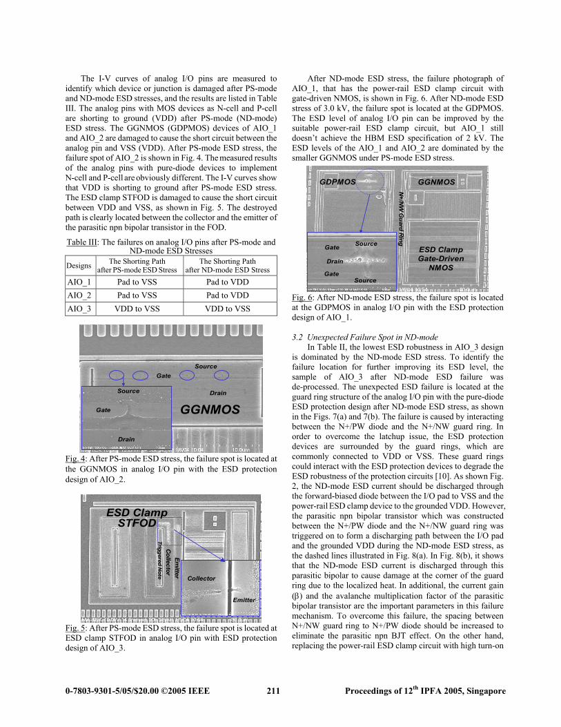
After ND-mode ESD stress, the failure photograph of AIO_1, that has the power-rail ESD clamp circuit with gate-driven NMOS, is shown in Fig. 6. After ND-mode ESD stress of 3.0 kV, the failure spot is located at the GDPMOS. The ESD level of analog I/O pin can be improved by the suitable power-rail ESD clamp circuit, but AIO_1 still doesn’t achieve the HBM ESD specification of 2 kV. The ESD levels of the AIO_1 and AIO_2 are dominated by the smaller GGNMOS under PS-mode ESD stress.
GDPMOS
ESD Clamp Gate-Driven
NMOS
N+/N
W G
uard Ring
GGNMOS
Gate Source
Drain
SourceGate
Fig. 6: After ND-mode ESD stress, the failure spot is located at the GDPMOS in analog I/O pin with the ESD protection design of AIO_1. 3.2 Unexpected Failure Spot in ND-mode
In Table II, the lowest ESD robustness in AIO_3 design is dominated by the ND-mode ESD stress. To identify the failure location for further improving its ESD level, the sample of AIO_3 after ND-mode ESD failure was de-processed. The unexpected ESD failure is located at the guard ring structure of the analog I/O pin with the pure-diode ESD protection design after ND-mode ESD stress, as shown in the Figs. 7(a) and 7(b). The failure is caused by interacting between the N+/PW diode and the N+/NW guard ring. In order to overcome the latchup issue, the ESD protection devices are surrounded by the guard rings, which are commonly connected to VDD or VSS. These guard rings could interact with the ESD protection devices to degrade the ESD robustness of the protection circuits [10]. As shown Fig. 2, the ND-mode ESD current should be discharged through the forward-biased diode between the I/O pad to VSS and the power-rail ESD clamp device to the grounded VDD. However, the parasitic npn bipolar transistor which was constructed between the N+/PW diode and the N+/NW guard ring was triggered on to form a discharging path between the I/O pad and the grounded VDD during the ND-mode ESD stress, as the dashed lines illustrated in Fig. 8(a). In Fig. 8(b), it shows that the ND-mode ESD current is discharged through this parasitic bipolar to cause damage at the corner of the guard ring due to the localized heat. In additional, the current gain (β) and the avalanche multiplication factor of the parasitic bipolar transistor are the important parameters in this failure mechanism. To overcome this failure, the spacing between N+/NW guard ring to N+/PW diode should be increased to eliminate the parasitic npn BJT effect. On the other hand, replacing the power-rail ESD clamp circuit with high turn-on
0-7803-9301-5/05/$20.00 ©2005 IEEE 212 Proceedings of 12th IPFA 2005, Singapore
efficiency can avoid the parasitic npn turn-on to degrade the ESD robustness under ND-mode ESD stress. A successful modification with optimal power-rail ESD clamp circuit has been practically verified in a 0.13-µm CMOS process to achieve HBM ESD level of 7.0 kV for analog I/O cell.
P+/NW Diode N+/PW Diode
ESD Clamp STFOD
N+/N
W G
uard Ring
(a)
N+/N
W G
uard Ring
P+ Diffusion
N+ Diffusion
N+/PW Diode
(b)
Fig. 7: (a) After ND-mode ESD stress, the failure spot is located at the guard ring in AIO_3. (b) The zoomed-in view of the failure spot at the guard ring corner.
NW
N+
VDD VSS
P-substrate
N+P+
I/O Pad
ESD Protection N+/PW Diode
Base EmitterCollectorGuard RingParasitic npn BipolarParasitic npn Bipolar
PW
(a)
Pad Internal circuits
ESD C
lamp
STFOD
Parasitic npn Bipolar
N+
PW
N+/NW Guard Ring
VDD
VSS
ND-mode
(b)
Fig. 8: (a) The parasitic npn bipolar was constructed between the N+/PW diode and N+/NW guard ring. (b) The ESD current discharged through the parasitic npn bipolar to grounded VDD during the ND-mode ESD stress causes the unexpected ESD failure.
4. Conclusion Different ESD protection schemes for the analog
input/output cells have been investigated to find the optimal analog ESD protection design for deep-submicron CMOS technology. According to the experimental results, the GGNMOS was not a suitable ESD protection device for analog I/O cells in deep-submicron CMOS process, such as 0.18-µm and below. The pure-diode ESD protection device between the pad to VDD (VSS) would be an optimal design for the analog I/O pins. In addition, the gate-driven NMOS for power-rail ESD clamp circuit also performs a higher ESD robustness for analog I/O pins in deep-submicron CMOS technology with STI structure. Finally, layout optimization with a wider spacing between N+/PW diode and N+/NW guard ring, as well as improvement on the power-rail ESD clamp circuit with high turn-on efficiency, should be used to avoid the unexpected ESD failure under ND-mode ESD stress in such analog I/O cells.
References [1] S. Voldman, “The state of the art of electrostatic
discharge protection: physics, technology, circuits, design, simulation, and scaling,” IEEE J. of Solid-State Circuits, vol. 34, no. 9, pp. 1272-1282, 1999.
[2] C. Duvvury and A. Amerasekera, “ESD: a pervasive reliability concern for IC technologies,” Proc. IEEE, vol. 81, pp. 690-702, 1993.
[3] A. Amerasekera and C. Duvvury, “The impact of technology scaling on ESD robustness and protection circuit design,” in Proc. of EOS/ESD Symp., 1994, pp. 237-245.
[4] S. Daniel and G. Krieger, “Process and design optimization for advanced CMOS I/O ESD protection devices,” in Proc. of EOS/ESD Symp., 1990, pp. 206-213.
[5] S. G. Beebe, “Methodology for layout design and optimization of ESD protection transistors,” in Proc. of EOS/ESD Symp., 1996, pp. 265-275.
[6] M.-D. Ker, T.-Y. Chen, C.-Y. Wu, and H.-H. Chang, “ESD protection design on analog pin with very low input capacitance for high-frequency or current-mode applications,” IEEE J. of Solid-State Circuits, vol. 35, no. 8, pp. 1194-1199, 2000.
[7] R. Merrill and E. Issaq, “ESD design methodology,” in Proc. of EOS/ESD Symp., 1993, pp. 233-237.
[8] M.-D. Ker, “Whole-chip ESD protection design with efficient VDD-to-VSS ESD clamp circuit for submicron CMOS VLSI,” IEEE Trans. Electron Devices, vol. 46, pp. 173-183, Jan. 1999.
[9] M.-D. Ker, “Area-efficient VDD-to-VSS ESD protection circuit,” US patent #5,744,842, Apr. 1998.
[10] D. Tremouilles, G. Bertrand, M. Bafleur, F. Beaudoin, P. Prerdu, N. Guitard, and L. Lescouzeres, “TCAD and SPICE modeling help solve ESD protection issues in analog CMOS technology,” Microelectronics Reliability, vol. 43, pp. 71-79, 2003.