a multi-cell switch-mode power-supply concept … · a multi-cell switch-mode power-supply concept...
TRANSCRIPT
A Multi-Cell Switch-Mode Power-Supply ConceptFeaturing Inherent Input Voltage Balancing
K. EDELMOSER H. ERTL F. ZACHInstitute of Electrical Drives and Machines – Power Electronics Section
Vienna University of TechnologyGusshausstrasse 27/372, A-1040 Vienna
Austria
Abstract: – A novel switch-mode power supply (SMPS) concept is presented which is especially suited to highinput voltages. The topology is based on a multi-cell arrangement where individual DC-DC converter cells areconnected in series regarding their input side whereas the isolated output stages of the cells are connected inparallel. The identical cells are realized as self-oscillating series-resonant converters operated at near unityduty cycle. Consequently, the cell only performs an isolation function, the voltage regulation is realized by asubsequent non-isolated DC-DC converter at low voltage level. The isolation stage is based on the well knownhalf-bridge topology utilizing efficient standard medium-voltage MOSFETs. A very interesting feature of theproposed system is that it is characterized by an inherent equalizing of the input voltage of the individual cellswithout any control requirements. The paper gives a short introduction to the basic problems of SMPS for highinput voltages, describes the basic operation of the presented topology and gives a dimensioning as well assimulation results and presents measurement results taken from a laboratory prototype.
Key-Words: – switch-mode power supply, SMPS, multi-cell topology, voltage balancing
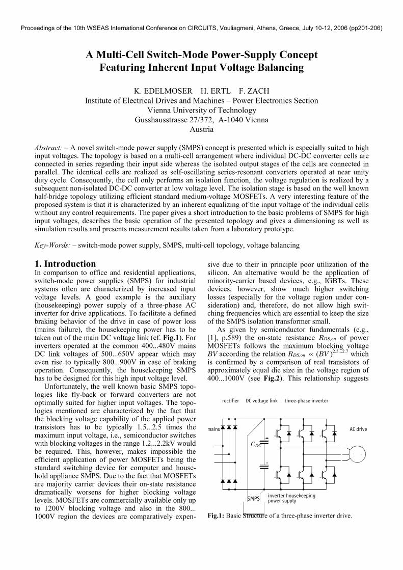
1. IntroductionIn comparison to office and residential applications,switch-mode power supplies (SMPS) for industrialsystems often are characterized by increased inputvoltage levels. A good example is the auxiliary(housekeeping) power supply of a three-phase ACinverter for drive applications. To facilitate a definedbraking behavior of the drive in case of power loss(mains failure), the housekeeping power has to betaken out of the main DC voltage link (cf. Fig.1). Forinverters operated at the common 400...480V mainsDC link voltages of 500...650V appear which mayeven rise to typically 800...900V in case of brakingoperation. Consequently, the housekeeping SMPShas to be designed for this high input voltage level.
Unfortunately, the well known basic SMPS topo-logies like fly-back or forward converters are notoptimally suited for higher input voltages. The topo-logies mentioned are characterized by the fact thatthe blocking voltage capability of the applied powertransistors has to be typically 1.5...2.5 times themaximum input voltage, i.e., semiconductor switcheswith blocking voltages in the range 1.2...2.2kV wouldbe required. This, however, makes impossible theefficient application of power MOSFETs being thestandard switching device for computer and house-hold appliance SMPS. Due to the fact that MOSFETsare majority carrier devices their on-state resistancedramatically worsens for higher blocking voltagelevels. MOSFETs are commercially available only upto 1200V blocking voltage and also in the 800...1000V region the devices are comparatively expen-
sive due to their in principle poor utilization of thesilicon. An alternative would be the application ofminority-carrier based devices, e.g., IGBTs. Thesedevices, however, show much higher switchinglosses (especially for the voltage region under con-sideration) and, therefore, do not allow high swit-ching frequencies which are essential to keep the sizeof the SMPS isolation transformer small.
As given by semiconductor fundamentals (e.g.,[1], p.589) the on-state resistance RDS,on of powerMOSFETs follows the maximum blocking voltageBV according the relation RDS,on ∝ (BV )2.5...2.7 whichis confirmed by a comparison of real transistors ofapproximately equal die size in the voltage region of400...1000V (see Fig.2). This relationship suggests
SMPS
DC voltage link three-phase inverterrectifier
inverter housekeeping power supply
AC drivemains
DCC
Fig.1: Basic Structure of a three-phase inverter drive.
Proceedings of the 10th WSEAS International Conference on CIRCUITS, Vouliagmeni, Athens, Greece, July 10-12, 2006 (pp201-206)
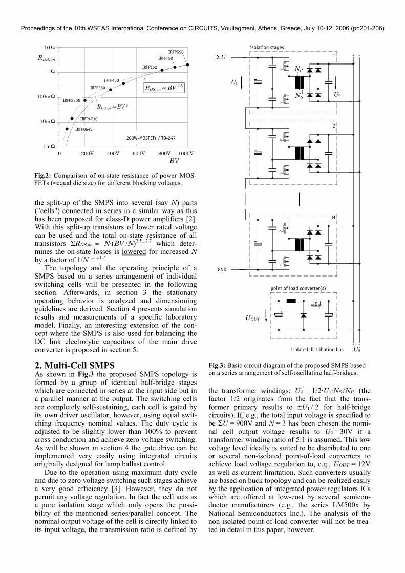
the split-up of the SMPS into several (say N) parts("cells") connected in series in a similar way as thishas been proposed for class-D power amplifiers [2].With this split-up transistors of lower rated voltagecan be used and the total on-state resistance of alltransistors ΣRDS,on ∝ N·(BV /N)2.5...2.7 which deter-mines the on-state losses is lowered for increased Nby a factor of 1/N 1.5...1.7.
The topology and the operating principle of aSMPS based on a series arrangement of individualswitching cells will be presented in the followingsection. Afterwards, in section 3 the stationaryoperating behavior is analyzed and dimensioningguidelines are derived. Section 4 presents simulationresults and measurements of a specific laboratorymodel. Finally, an interesting extension of the con-cept where the SMPS is also used for balancing theDC link electrolytic capacitors of the main driveconverter is proposed in section 5.
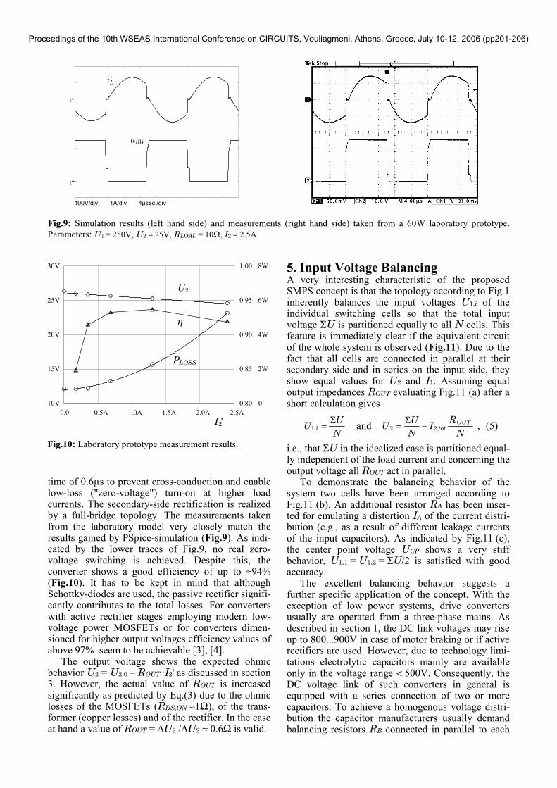
2. Multi-Cell SMPSAs shown in Fig.3 the proposed SMPS topology isformed by a group of identical half-bridge stageswhich are connected in series at the input side but ina parallel manner at the output. The switching cellsare completely self-sustaining, each cell is gated byits own driver oscillator, however, using equal swit-ching frequency nominal values. The duty cycle isadjusted to be slightly lower than 100% to preventcross conduction and achieve zero voltage switching.As will be shown in section 4 the gate drive can beimplemented very easily using integrated circuitsoriginally designed for lamp ballast control.
Due to the operation using maximum duty cycleand due to zero voltage switching such stages achievea very good efficiency [3]. However, they do notpermit any voltage regulation. In fact the cell acts asa pure isolation stage which only opens the possi-bility of the mentioned series/parallel concept. Thenominal output voltage of the cell is directly linked toits input voltage, the transmission ratio is defined by
the transformer windings: U2'= 1/2·U1·NS /NP (the
factor 1/2 originates from the fact that the trans-former primary results to ±U1 / 2 for half-bridgecircuits). If, e.g., the total input voltage is specified tobe ΣU = 900V and N = 3 has been chosen the nomi-nal cell output voltage results to U2
'= 30V if atransformer winding ratio of 5:1 is assumed. This lowvoltage level ideally is suited to be distributed to oneor several non-isolated point-of-load converters toachieve load voltage regulation to, e.g., UOUT
= 12Vas well as current limitation. Such converters usuallyare based on buck topology and can be realized easilyby the application of integrated power regulators ICswhich are offered at low-cost by several semicon-ductor manufacturers (e.g., the series LM500x byNational Semiconductors Inc.). The analysis of thenon-isolated point-of-load converter will not be trea-ted in detail in this paper, however.
0 200V 400V 600V 800V 1000V
10IRFPG50
Ω
1Ω
100mΩ
10mΩ
1mΩ
IRFP064V
IRFP4710
IRFP250N
\
200W-MOSFETs / TO-247
IRFPE52
IRFP360
IRFP450
\\
IRFPF50 \\
\onDSR ,
BV
5.2, BVR onDS ∞
2, BVR onDS ∞
Fig.2: Comparison of on-state resistance of power MOS-FETs (≈equal die size) for different blocking voltages.
1U
'2U
PN
SN
isolation stages
1
2
N
point of load converter(s)
OUTU
ΣU
'2Uisolated distribution bus
GND
Fig.3: Basic circuit diagram of the proposed SMPS basedon a series arrangement of self-oscillating half-bridges.
Proceedings of the 10th WSEAS International Conference on CIRCUITS, Vouliagmeni, Athens, Greece, July 10-12, 2006 (pp201-206)

3. Stationary Operating CharacteristicThe isolation stages are operated in series-resonantmode with capacitive output filtering. This mode hasbeen chosen due to the expected good efficiencybased on the near unity duty cycle and the zero-voltage turn-on of the power transistors. Further-more, the blocking voltage stress on all semicon-ductors is well defined and the transformer leakage Lcan be utilized as resonance inductance. Therefore,as opposed to, e.g., transformers for flyback conver-ters a certain amount of leakage is of advantage here.
In the following, the characteristics of the statio-nary operation shall be calculated. To simplify theconsiderations the total cell input voltage here shallbe denoted as 2U1 (Fig.4). The system is charac-terized by different conduction states (A→B→C→D)defined by the polarities of the input voltage u1 andof the reflected secondary voltage u2. Whereas thepolarity of u1 is defined by the control circuit, thepolarity of u2 is determined by the direction of theresonant current iL. For state A, u1 and u2 show equaldirection and the (small) difference ∆U = U1 −U2 isapplied to the LC series resonant circuit. This resultsin a circular shaped system trajectory around thecenter point [+∆U,0] (cf. uCZ0iL-diagram of Fig.5 (a),Z0 = CL / defines the characteristic impedance of theresonant network). Because the system operates witha switching frequency fS above the natural frequencyf0 =1/(2π LC ), the input voltage u1 changes its polari-ty at instant 1 due to the turn-off of the high-sidetransistor before iL becomes zero. Consequently, thesystem transits to state B where the sum U1 +U2
causes a steep current reduction (cf. Fig.5 (b)) accor-ding to the circular trajectory with the center point[−(U1 +U2),0]. At instant 2, the current iL becomesnegative, the current in the rectifier diodes commuta-tes and u2 again shows equal (i.e., negative) polarityas u1 (state C); now [−∆U,0] is the new center of thetrajectory valid until the lower power transistor turnsoff at instant 3 and the system passes over to state D(center [U1 +U2,0]) which completes a full cycle ininstant 4.
For the practical realization of the converter it isof importance that, in general, U1 +U2 >>∆U is valid.With this assumption the system trajectory in goodapproximation shows the shape of Fig.5 (c), i.e., thecurrent contribution of states B and D to i2 can beneglected (t1,2 → 0, Fig.5 (c)). With this and using theconduction angle α = π / (fS /f0) the equations
(1)and
(2)
can be derived according to the geometrical relationsgiven by Fig.5 (c) and according to the fact that theaverage value of i2 (i.e., the rectified inductor currentiL) in the stationary case is defined by the loadcurrent I2. Evaluation of Eq.(2) and rearranging usingEq.(1) finally leads to
with (3)
and . (4)
1U
'2U
CuU +1
L
C21
C21
1U
1U
2U
LiCu
1u 2u
Li
L
C
1u 2u
L
C
LiCu
Sf 2i
(a)
(b)
(c)
2
'2I
Fig.4: Schematic diagram of the series-resonant converter(a) and corresponding equivalent circuits (b), (c).
21 UU +
Cu
LiZ0
U∆
A
B
C
D
(a)
1u
2u
t
Li
t
t
A C
B DD
(b)
1
21 2
3
43 4
LiZ0
CuU∆
α
CuCu(c)
tω
π
Li
2i2I
α
Li
tω
(d)
1,2t
1
2
TURN-OFFMOSFET
Fig.5: System trajectory (a) and time behavior (b) of theseries resonant converter; (c), (d): simplification valid forU1 +U2 >>∆U; i2: output current of the rectifier (Fig.4 (b)).
tdtUuIZ C ωωαα
)sin(1)ˆ(0
20 ∫∆+=
UuUu CC ∆−=−∆+ ˆ)cos()ˆ( απ
ααα
cos1cos1
20 −
+= ZROUTOUTRIU ⋅=∆ 2
CfI
ZIuS
C42
ˆ 202 =⋅⋅= α
Proceedings of the 10th WSEAS International Conference on CIRCUITS, Vouliagmeni, Athens, Greece, July 10-12, 2006 (pp201-206)

These equations state that for a given switching fre-quency (i.e., a fixed conduction interval α) the outputvoltage U2 decreases proportional to the load currentI2, the converter shows a quasi-ohmic (non-dissipa-tive!) output impedance (current-independent outputresistance ROUT, cf. equivalent circuit given in Fig.6,where Eqs. (3) and (4) are evaluated graphically).Due to the fact that ROUT mainly is determined via Z0
by L (the transformer leakage inductance), its valueusually is comparatively low related to the nominalload resistance U2/I2. The appearing load voltagedrop ∆U = ROUT ·I2 easily can be corrected by thepoint-of-load converter. On the other hand, the non-zero value of ROUT is essential for the applicabilityof this concept, because it guarantees the currentsharing of all cells and with this, in an indirectmanner, the balancing of the individual input vol-tages of the series connected cells.
4. Dimensioning ExampleAs is indicated by Fig.5 (d), a dimensioning using ahigh value of α would be of advantage since thecurrent which the MOSFETs have to switch-off isreduced as a fact of the resonance principle (iL→0).A value of α = 150°...170°, however, gives a verylow ROUT (cf. Fig.6) which worsens the currentsharing. Furthermore, ROUT also acts as a (non-dissi-pative!) damper for the resonant circuit. For apractical realization, therefore, a dimensioning ofα =120° (i.e., fS =1.5f0 ) is a good trade-off leading toROUT = π/9·Z0 ≈0.35·Z0.
Due to the high input voltage level the converterhas to have a very good isolation barrier. Therefore, atransformer is applied which features a strict separa-tion of the windings. Electronic ballasts for low-vol-tage halogen lamps very often are equipped with atoroid transformer where the primary and secondarywindings are separated very strictly by different coilformer elements. The primary winding shows a fullencapsulation, the isolated secondary winding islocated at the transformer surface (Fig.7). Despite the
fact that this component is a low-cost device, thetransformer shows very good electrical parameters.Its sole "drawback", the somewhat increased strayinductance is rather of advantage for this application.The applied transformer, based on a ∅25x14mmtoroid core is characterized by the parameters:
primary: 80 turns L1 = 30mHsecondary: 2x8 turns L2 = 1.2mHleakage (primary side): L = 35µH.
Both secondary windings are connected in series toget a 5:1 transformation ratio in order to receive theaimed 10:1 input-to-output voltage ratio. If a swit-ching frequency of fS = 50kHz and α=120° arechosen, one gets for the residual parameters:
natural frequency: f0 = 50kHz / 1.5 ≈ 33kHzresonance capacitors: C = 2 x 0.33µFcharacteristic impedance: Z0 = 7.3Ωoutput imp. (primary side): ROUT = 2.5Ω.
As depicted in Fig.8 the control of the convertershows a very low effort if an integrated gate drive IC(IR21531D, originally designed for energy savinglamps) is applied. The operating frequency is set byRT and CT; the IC provides an internal fixed dead
30° 60° 90° 120° 150° 180°0.0
0.5
1.0
1.5
2.0
1.0
1.5
2.0
2.5
3.0
α
0ZROUT
0ffS
20
ˆIZ
uC
1U 2UOUTR
Fig.6: Dependency of the characteristic dimensioning para-meters on the conduction interval α.
Fig.7: Toroid transformer as used in halogen lamp ballasts.Primary winding fully encapsulated.
IR21531D
VCC HO
COM
CT
RT
VB
VS
LO
4 x 21DQ06
2 x IRF730
0.33µF
0.33µF
35µH
5:1
Li
'2U
1U
SWu
Fig.8: Schematic diagram of the power circuit.
Proceedings of the 10th WSEAS International Conference on CIRCUITS, Vouliagmeni, Athens, Greece, July 10-12, 2006 (pp201-206)
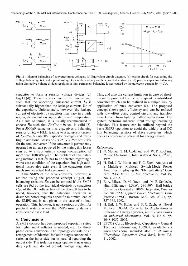
time of 0.6µs to prevent cross-conduction and enablelow-loss ("zero-voltage") turn-on at higher loadcurrents. The secondary-side rectification is realizedby a full-bridge topology. The measurements takenfrom the laboratory model very closely match theresults gained by PSpice-simulation (Fig.9). As indi-cated by the lower traces of Fig.9, no real zero-voltage switching is achieved. Despite this, theconverter shows a good efficiency of up to ≈94%(Fig.10). It has to be kept in mind that althoughSchottky-diodes are used, the passive rectifier signifi-cantly contributes to the total losses. For converterswith active rectifier stages employing modern low-voltage power MOSFETs or for converters dimen-sioned for higher output voltages efficiency values ofabove 97% seem to be achievable [3], [4].
The output voltage shows the expected ohmicbehavior U2 = U2,0 − ROUT ·I2' as discussed in section3. However, the actual value of ROUT is increasedsignificantly as predicted by Eq.(3) due to the ohmiclosses of the MOSFETs (RDS,ON ≈1Ω), of the trans-former (copper losses) and of the rectifier. In the caseat hand a value of ROUT = ∆U2 /∆U2 ≈ 0.6Ω is valid.
5. Input Voltage BalancingA very interesting characteristic of the proposedSMPS concept is that the topology according to Fig.1inherently balances the input voltages U1,i of theindividual switching cells so that the total inputvoltage ΣU is partitioned equally to all N cells. Thisfeature is immediately clear if the equivalent circuitof the whole system is observed (Fig.11). Due to thefact that all cells are connected in parallel at theirsecondary side and in series on the input side, theyshow equal values for U2 and I1. Assuming equaloutput impedances ROUT evaluating Fig.11 (a) after ashort calculation gives
and , (5)
i.e., that ΣU in the idealized case is partitioned equal-ly independent of the load current and concerning theoutput voltage all ROUT act in parallel.
To demonstrate the balancing behavior of thesystem two cells have been arranged according toFig.11 (b). An additional resistor RA has been inser-ted for emulating a distortion IA of the current distri-bution (e.g., as a result of different leakage currentsof the input capacitors). As indicated by Fig.11 (c),the center point voltage UCP shows a very stiffbehavior, U1,1 = U1,2 = ΣU/2 is satisfied with goodaccuracy.
The excellent balancing behavior suggests afurther specific application of the concept. With theexception of low power systems, drive convertersusually are operated from a three-phase mains. Asdescribed in section 1, the DC link voltages may riseup to 800...900V in case of motor braking or if activerectifiers are used. However, due to technology limi-tations electrolytic capacitors mainly are availableonly in the voltage range < 500V. Consequently, theDC voltage link of such converters in general isequipped with a series connection of two or morecapacitors. To achieve a homogenous voltage distri-bution the capacitor manufacturers usually demandbalancing resistors RB connected in parallel to each
100V/div 1A/div 4µsec./div
SWu
Li
Fig.9: Simulation results (left hand side) and measurements (right hand side) taken from a 60W laboratory prototype.Parameters: U1 = 250V, U2 ≈ 25V, RLOAD = 10Ω, I2 ≈ 2.5A.
0.0 0.5A 1.0A 1.5A 2.0A 2.5A10V
15V
20V
25V
30V
0.80
0.85
0.90
0.95
1.00
'2I
2U
η
0
2W
4W
6W
8W
LOSSP
Fig.10: Laboratory prototype measurement results.NU
U iΣ=,1
NR
INU
U OUTtot,22 −Σ=
Proceedings of the 10th WSEAS International Conference on CIRCUITS, Vouliagmeni, Athens, Greece, July 10-12, 2006 (pp201-206)
capacitor to form a resistor voltage divider (cf.Fig.11 (d)). These resistors have to be dimensionedsuch that the appearing quiescent current IQ issubstantially higher than the leakage currents ILL ofthe capacitors. Unfortunately, however, the leakagecurrent of electrolytic capacitors may vary in a wideregion, dependent on aging status and temperature.As a rule of thumb, it is usually recommended tochoose RB such that RB·CDC ≈ 50 sec. is valid [5].For a 5000µF capacitor this, e.g., gives a balancingresistor of RB = 10kΩ leading to a quiescent currentof IQ =25mA (@250V capacitor voltage) and resul-ting in additional losses of 2 x 250V x 25mA=12.5Wfor the total converter. If the converter is permanentlyoperated or at least powered by the mains, this lossessum up to a substantially energy consumption ofmore than 100kWh/year! The problem of this balan-cing method is that RB has to be selected regarding aworst-case condition of the capacitors but high addi-tional losses also exist even if the capacitors showmuch smaller actual leakage currents.
If the SMPS of the drive converter, however, isrealized using the proposed concept (Fig.2), thebalancing resistors RB can be omitted if the SMPScells are fed by the individual electrolytic capacitorsCDC of the DC voltage link of the drive. It has to benoted, however, that the balancing operation asdescribed before requires a specific minimum load ofthe SMPS and is not given in the case of no-loadoperation. This, however, is not a serious problem forpractical systems where the SMPS usually shows aconsiderable basic load.
6. ConclusionsA SMPS concept has been proposed especially suitedfor higher input voltages as needed, e.g., for three-phase drive converters. The topology consists of anarrangement of identical isolation stages connected inseries at the input side but in parallel regarding theoutput side. The isolation stages operate at near unityduty cycle and do not provide voltage regulation.
This, and also the current limitation in case of short-circuit is provided by the subsequent point-of-loadconverter which can be realized in a simple way byapplication of buck converter ICs. The proposedconcept shows good efficiency and can be realizedwith low effort using control circuits and transfor-mers known from lighting ballast applications. Thesystem performs inherent input voltage balancingbehavior. This feature can be utilized beyond thebasic SMPS operation to avoid the widely used DClink balancing resistors of drive converters whichopens a considerable potential for energy saving.
References:[1] N. Mohan, T. M. Undeland and W. P. Robbins,
Power Electronics, John Wiley & Sons, 2nd ed.,1995.
[2] H. Ertl, J. W. Kolar and F. C. Zach, Analysis ofa Multilevel Multicell Switch-Mode PowerAmplifier Employing the "Flying-Battery" Con-cept, IEEE Trans. on Ind. Electronics, Vol. 49,No. 4, 2002.
[3] B. A. Miwa, D. M. Otten and M. E. Schlecht,High-Efficiency 1.5kW, 390-50V Half-bridgeConverter Operated at 100% Duty-ratio, Proc. ofthe 7th IEEE Applied Power Electronics Con-ference (APEC), Boston, MA, Feb. 23-27, pp.557-568, 1992.
[4] H. Ertl, J. W. Kolar and F. C. Zach, A NovelMulticell DC-AC Converter for Applications inRenewable Energy Systems, IEEE Transactionson Industrial Electronics, Vol. 49, No. 5, pp.1048-1057, 2002.
[5] EPCOS Corp., Electrolytic Capacitors – GeneralTechnical Information, 10/2002, available viawww.epcos.com, included also in AluminumElectrolytic Capacitors Data Book, latest Ed.11, 2002.
iU ,1
1,1U
NU ,1
totI ,2
2U
UΣ
0
1:1
OUTR
1:1
OUTR
1:1
OUTR
2I 2I
(a)(d)
AR
BR BR
CPUAI
QI
0
10mA
55mA
45mA
+200V55mA
10
1
10
1
550mA
450mA
1A
100V
Ω10k (b)
0 10 20 30 40 5098
99
100
101
102CPU
[ V ]
AI[ mA ]
≈CPiR , 25Ω
(c)
CPiACP RIU ,⋅=∆
LLI
Fig.11: Inherent balancing of converter input voltages. (a) Equivalent circuit diagram, (b) testing circuit for evaluating thevoltage balancing, (c) center point voltage UCP in dependency on the current distortion IA, (d) passive capacitor balancingusing dissipative voltage divider resulting in high permanent balancing losses caused by the quiescent current IQ >> ILL.
Proceedings of the 10th WSEAS International Conference on CIRCUITS, Vouliagmeni, Athens, Greece, July 10-12, 2006 (pp201-206)