a high-speed three -stage cmos op amplifier with a … · using a conventional two-stage op amp...
TRANSCRIPT

Abstract—A high-speed three-stage CMOS OP Amp with a
dynamic switching bias circuit, capable of processing video signals of over 2 MHz, is presented to provide slight nonlinearity through the achievement of higher gain while maintaining high-speed switching operation and low power dissipation. The designed OP Amp, capable of operating at 10 MHz dynamic switching rate, and through simulations showed a dissipated power of 60 % of that in conventional continuous operation. A switched capacitor (SC) non-inverting amplifier with a gain of 2 employing this OP Amp and its high-speed 10 MHz dynamic switching operation, capable of processing video signals, is demonstrated. Its power dissipation decreased to 62 % of that in normal operation when the switching duty ratio was increased to 70 %. The output voltage inaccuracy for a SC amplifier with a gain of less than 2 decreased to below 1 %, one sixth of that using a conventional two-stage OP Amp with the dynamic switching bias circuit, mainly caused by the static nonlinearity of the OP Amp. This circuit configuration will be extremely useful in realizing low-power wide-band signal processing ICs.
Index Terms—switched capacitor circuit, CMOS, operational amplifier, dynamic switching
I. INTRODUCTION
n recent years, the trend of IC development has been moving toward lower power consumption using low power
supply voltages and short channel CMOS technologies. The purpose of this move is to achieve portable equipment using audio signal processors or video signal processors for use in video electrical appliances. However, although digital video signal processors (real time image processors) with functions such as coding, vector quantization, motion compensation, filtering, and similar have been developed [1,2], the chip size of these processors is large. Such processors also have the disadvantage of operating at very large power consumption of over 1 W. Furthermore, they also need A/D (analog-to- digital) and D/A (digital-to-analog) conversion circuits, which results in large power consumption when they are integrated with main processors.
In contrast, the switched capacitor (SC) technology enables analog signal processing without the use of A/D and D/A conversion circuits, and has been mainly applied to filters of low frequency, such as a few hundred kHz, suitable for audio
Manuscript received July 20, 2013; revised November 25, 2013. This work was supported by the Foundation for the Education Research Program in Tokyo Metropolitan College of Industrial Technology. H. Wakaumi is with the Division of Electronics and Information Engineering, Tokyo Metropolitan College of Industrial Technology, 1-10-40 Higashi-Ooi, Shinagawa, Tokyo, 140-0011 Japan (corresponding author to provide phone: +81-3-3471-6331; fax: +81-3-3-471-6338; e-mail: [email protected]).
signal processors [3-5]. CMOS SC technology has promising use in video signal bandwidth circuits in particular, because one can easily integrate complicated systems into a single chip IC at low cost using this technology. In this paper, the author focuses on SC technology because it has potential for low-power and high-speed operation. It has been demonstrated that SC techniques using CMOS operational amplifiers (OP Amps) are useful for implementing efficient measures with analog functions such as filtering [6,7]. Although CMOS OP Amps are suitable for such filter ICs, the use of several OP Amps results in large power dissipation (causing unstable operation). A high speed CMOS OP Amp consisting of a fully differential operational transconductance amplifier (OTA) with two pairs of folded cascode OP Amps and a common-mode-feedback (CMFB) circuit has recently been developed [8]. This fully differential two-stage OTA, was applied to high-gain and high-speed operations of SC applications, and demonstrated a low power dissipation of 10 mW at a relatively high slew rate of 340 V/μs with a power supply voltage of 2 V. However, its circuit, which included several OP Amps, was too complicated for the signal processing IC, and so required a larger chip area and larger power dissipation. Therefore, a simple OP Amp configuration that enables smaller power dissipation and smaller chip area, even when the number of OP Amps increases, is desirable for large-scale ICs for multi-functional analog processing.
Until now, several approaches have been taken to decrease the power consumption of OP Amps, including the development of ICs that work at low power supply voltages. A clocked current bias scheme for folded cascode OP Amps has typically been proposed to decrease the power consumption of the OP Amp itself [9,10]. In such a circuit, each bias current for the slewing, settling, and holding phases is dynamically controlled by a multi bias current control method with clocked current sources. Even using this scheme, however, the maximum ratio of the total power savings is limited to near 30 %. Because the circuit also requires complicated four-phase bias-current control pulses and biasing circuits, it results in a large layout area and is not suitable for the high-speed operation.
A control method using power supply switching has been proposed for audio signal processing as another approach to decreasing the power consumption of OP Amps [11]. Because large capacitances for the power supply terminals are intrinsically loaded, the switching speed is limited to a low speed of 1 MHz at most. Therefore, this type of control circuit is not suitable for application to video signal processing ICs, which are required to operate at over 10 MHz switching frequency.
The author previously proposed a two-stage CMOS OP Amp with a dynamic switching bias (DSB) circuit, of simple configuration, to provide low power dissipation while
A High-Speed Three-Stage CMOS OP Amplifier with a Dynamic Switching Bias Circuit
Hiroo Wakaumi, Member, IAENG
I
Engineering Letters, 21:4, EL_21_4_08
(Advance online publication: 29 November 2013)
______________________________________________________________________________________

maintaining high speed switching operation suitable for processing video signals [12]. However, there is a problem remaining in that reduction of its slightly large nonlinearity, caused by the low gain of the OP amp, is required for practical use.
In this paper, a new three-stage CMOS OP Amp employing the DSB circuit with a simple configuration [13] which provides slight nonlinearity through higher gain while maintaining high-speed switching operation suitable for processing video signals and low power dissipation, is presented. This OP Amp can even operate at low supply voltages as is possible with the conventional two-stage amp, because of its non-cascode configuration.
II. DSB THREE-STAGE OP AMP
The function of switched capacitor amplifiers is basically equivalent to a resistor-type amp consisting of two resistors and an OP Amp, except for providing analog signals in the discrete-time domain. Thus, the well-known resistor-type inverting amp (Fig. 1) is here considered to determine the optimum OP Amp configuration. Considering that the ideal absolute gain of the inverting amp is described as R2/R1 when the gain of the OP Amp is infinite, the inaccuracy ε’ correspondent to nonlinear distortion for this amp is generally given by Equation (1).
||]
)
2
/()
2
1)(2
1
21(1
11[
1R
2R' iV
R
oRA
LR
oR
R
oR
iR
R
R
R⋅
−+++++
−=ε (1)
Where Vi, Ri, Ro, RL, and A represent the input voltage, the input impedance of the OP Amp, the output impedance of the OP Amp, the load resistance, and the gain of the OP Amp, respectively. It is apparent that the inaccuracy ε’ approaches 0 as A increases. Thus, the addition of an inverting amplifier to the two-stage CMOS OP Amp is attempted as an approach to reduce nonlinear distortion. Figure 2 shows a three-stage CMOS OP Amp configuration with the DSB circuit. The OP Amp consists of a current-mirror differential amplifier M5-M9, an inverting amplifier M10-M11 inserted to perform higher gain, an output amplifier M13-M14 with a compensation capacitor Cc and a compensation n-MOS FET M12 added as a resistor, and a DSB circuit to dynamically turn the current source M5, the inverting amplifier load M11, and the output amplifier load M14 on and off. The following circuit configuration for the proposed OP Amp is considered based on the conventional DSB two-stage OP Amp. That is, the compensation FET M12 is provided in addition to the compensation capacitor Cc to prevent the OP Amp from ringing or oscillating. A reduction in gain in the current- mirror differential amplifier and an increase in output impedance in the output amplifier are also performed for the prevention of ringing or oscillating. Furthermore, a reduction of output impedance in the DSB switching circuit is carried out to enable it to drive slightly larger loads of combined M5, M11 and M14 at high speed.
During the DSB operation, when a control pulse φB with a voltage swing of (−5 V) − (5 V) becomes −5 V, the OP Amp turns on by setting a bias voltage VB at an appropriate level by enabling M3 and M4 to operate in the saturation region, and
Fig. 1. Resistor-type inverting amp configuration.
Fig. 2. Configuration of the three-stage CMOS OP Amp with a DSB circuit. operates normally as an operational amplifier. Conversely, when φB becomes 5 V, the OP Amp turns off by setting VB at nearly −5 V. Therefore, the OP Amp does not dissipate at all during this off period. It is thus expected that the power dissipation becomes lower than that observed in usual continuous operation as for the conventional OP Amps.
III. SIMULATION RESULTS
Owing to the recent trend of aiming for decreased CMOS OP Amp power dissipation for use in portable equipment, attempts have been made to lower the power supply voltage of CMOS OP Amps. The reduction in operating speed caused by lowering the power supply voltage is compensated for by shortening the channel length of the CMOS FETs. 0.18−0.35 μm processes are currently used for OP Amp ICs [11,14]. Because the purpose of this study is to clarify the basic performance of OP Amps, ordinary CMOS FETs consisting of a minimum channel length of 2.5 μm, which is not influenced considerably by channel length modulation owing to process variation, are used. The MOSFET and capacitor elements of the OP Amp were designed as shown in Table I. Its performance was tested through SPICE simulations under the condition of the power supply voltages VDD=VSS=5 V. Typical performances compared with those of the conventional DSB OP Amp are shown in Table II. The open Table I. Designed channel length L and width W of the FETs and the value of the capacitor Cc.
Engineering Letters, 21:4, EL_21_4_08
(Advance online publication: 29 November 2013)
______________________________________________________________________________________
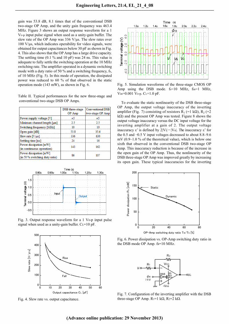
gain was 53.8 dB, 8.1 times that of the conventional DSB two-stage OP Amp, and the unity gain frequency was 463.4 MHz. Figure 3 shows an output response waveform for a 1 V0-p input pulse signal when used as a unity-gain buffer. The slew rate of the OP Amp was 336 V/μs. The slew rates over 100 V/μs, which indicates operability for video signals, were obtained for output capacitances below 30 pF as shown in Fig. 4. This also shows that the OP Amp has a large drive capacity. The settling time (0.1 % and 10 pF) was 24 ns. This value is adequate to fully settle the switching operation at the 10 MHz switching rate. The amplifier operated in a dynamic switching mode with a duty ratio of 50 % and a switching frequency, fs, of 10 MHz (Fig. 5). In this mode of operation, the dissipated power was reduced to 60 % of that observed in the static operation mode (143 mW), as shown in Fig. 6.
Table II. Typical performances for the new three-stage and conventional two-stage DSB OP Amps.
Fig. 3. Output response waveform for a 1 V0-p input pulse signal when used as a unity-gain buffer. CL=10 pF.
0
100
200
300
400
500
0 10 20 30 40 50 60
Sle
w r
ate [
V/μ
s]
Output capacitance CL [pF]
Rise
Fall
Fig. 4. Slew rate vs. output capacitance.
Fig. 5. Simulation waveforms of the three-stage CMOS OP Amp using the DSB mode. fs=10 MHz, fin=1 MHz, Vin=0.001 V0-p. CL=1.0 pF.
To evaluate the static nonlinearity of the DSB three-stage OP Amp, the output voltage inaccuracy of the inverting amplifier (Fig. 7) consisting of resistors R1 (=1 kΩ), R2 (=2 kΩ) and the present OP Amp was tested. Figure 8 shows the output voltage inaccuracy versus the DC input voltage for the inverting amplifier at a gain of 2. The output voltage inaccuracy ε’ is defined by 2|Vi|-|Vo|. The inaccuracy ε’ for the 0.5 and −0.5 V input voltages decreased to about 8.8–9.6 mV (0.9–1.0 % of the theoretical value), which is below one sixth that observed in the conventional DSB two-stage OP Amp. This inaccuracy reduction is because of the increase in the open gain of the OP Amp. Thus, the nonlinearity of the DSB three-stage OP Amp was improved greatly by increasing its open gain. These typical inaccuracies for the inverting
0
50
100
150
200
0 20 40 60 80
Pow
er d
issi
pation
Po [
mW
]
OP-Amp switching duty ratio TB/TS [%]
Static
Dynamic
Fig. 6. Power dissipation vs. OP-Amp switching duty ratio in the DSB mode OP Amp. fs=10 MHz.
Fig. 7. Configuration of the inverting amplifier with the DSB three-stage OP Amp. R1=1 kΩ, R2=2 kΩ.
Engineering Letters, 21:4, EL_21_4_08
(Advance online publication: 29 November 2013)
______________________________________________________________________________________

-0.02
0
0.02
0.04
0.06
0.08
-0.6 -0.4 -0.2 0 0.2 0.4 0.6
Outp
ut
voltag
e inac
cura
cy
ε'
[V]
DC input voltage Vi [V]
Fig. 8. Output voltage inaccuracy vs. DC input voltage for the inverting amplifier using the DSB three-stage OP Amp. The gain R2/R1 is 2. Table III. Typical inaccuracies for the inverting amplifier with a gain of 2, when using the new three-stage and conventional two-stage DSB OP Amps.
amplifier compared with those observed with conventional two-stage OP Amps are shown in Table III.
IV. APPLICATION TO SC AMP To demonstrate the practicability of the above DSB three-stage CMOS OP Amp, the feasibility of its application in a SC non-inverting amplifier, which can be used for processing circuits such as filters, was tested. Figures 9 and 10 show the SC non-inverting amplifier configuration and operation waveforms, respectively. When the sampling pulse φ2, one of complementary operating pulses (φ1 and φ2), changes from a low level (−5 V) to a high level (5 V), the amplified sampled input signal is output during the on-state of the OP Amp (φB is low). φB is set to low just before φ2 changes to high (10 ns was chosen for the transition delay time against the φB fall transition) such that the sampled input signal is amplified in the OP Amp in a stable manner. Operation waveforms with a gain (C1/C2) of 2 show that this OP Amp can operate within a video bandwidth of over 2 MHz at fs=10 MHz (Fig. 11). When the switching duty ratio TB/TS of the OP Amp was 50 %, its power dissipation was 75 % of that observed during static operation (Fig. 12). By increasing the duty ratio TB/TS to 70 %, its dissipated power decreased to 62 % of that observed during the static operation.
The accuracy of the output voltage was tested using parameters important in practical applications. Figure 13 shows the output voltage inaccuracy versus the OP Amp switching duty ratio in the SC amplifier with a gain of 2 compared with that for the conventional DSB two-stage OP Amp. The output voltage inaccuracy ε represents the difference between a theoretical value of the output voltage (gain × input voltage) and the actual output voltage. When the switching duty ratio TB/TS was 0−70 %, the inaccuracy ε for the 1 Vp-p input signal was nearly 0.01 V (~1 % of the
Fig. 9. Configuration of the SC non-inverting amplifier. φ1 and φ2 switches consist of CMOS FETs with W/L=25/2.5 (μm/μm).
Fig. 10. Operation waveforms of the SC amplifier.
Fig. 11. Simulation waveforms for the SC amplifier. C1=1.2 pF, C2=0.6 pF. ΔT=10 ns. Output load CO=1.0 pF. Input signal frequency=2 MHz.
0
50
100
150
200
0 20 40 60 80
Pow
er
diss
ipat
ion
Po [
mW
]
OP-Amp switching duty ratio TB/TS [%]
Static
Dynamic
Fig. 12. Power dissipation vs. OP-Amp switching duty ratio in the SC amplifier. fs=10 MHz, ΔT=10 ns. theoretical value), which is practically usable. This shows that the inaccuracy was reduced to one sixth of that observed for the conventional DSB two-stage OP Amp. This inaccuracy was caused by the nonlinearity in the static operation of the
Engineering Letters, 21:4, EL_21_4_08
(Advance online publication: 29 November 2013)
______________________________________________________________________________________

OP Amp, the additional nonlinearity in the dynamic operation of the OP Amp, and the nonlinearity in sampling circuits. To separate the cause of this inaccuracy, the dynamic operation was tested under the condition of static operation of the OP Amp (φB = −5 V). Figure 14 shows the output voltage inaccuracy versus the φ1 sampling pulse width for the SC amplifier. Despite the change in the sampling pulse width Tφ1, the inaccuracy ε was maintained at nearly 0.01 V, which was the same as that during dynamic OP Amp operation. This shows that there was hardly any additional nonlinearity in the dynamic operation of the OP Amp. Because the static nonlinearity in the OP Amp is 8−9 mV, we can state that the dynamic operational inaccuracy of the SC amplifier is mainly caused by the nonlinearity in the static operation of the OP Amp, and the dynamic operation inaccuracy in the sampling circuits and the OP Amp is low.
The gain dependency of the inaccuracy was tested by considering several OP Amps used in the form of different gains in the filters. Figure 15 shows the output voltage inaccuracy versus the SC amplifier gain C1/C2. The inaccuracy ε increased almost linearly with gain. These inaccuracies are below 1 % of their theoretical values within the gain of 2.
0
0.02
0.04
0.06
0.08
0 20 40 60 80
Out
put
voltag
e inac
cura
cy ε
[V
]
OP Amp switching duty ratio TB/TS [%]
Conventional DSB two-stage OP Amp
DSB three-stage OP Amp
Input=-0.5 V
Input=+0.5 V
Input=+0.5 V
Input=-0.5 V
Fig. 13. Output voltage inaccuracy vs. OP-Amp switching duty ratio in the SC amplifier. C1/C2=2. fs=10 MHz, ΔT=10 ns.
0
0.02
0.04
0.06
0.08
10 30 50 70 90
Out
put
voltag
e inac
cur
acy
ε [
V]
Sampling pulse width Tφ1 [ns]
Input= +0.5 V
Input= -0.5 V
Fig. 14. Output voltage inaccuracy vs. φ1 sampling pulse width for the SC amplifier using the static mode OP Amp. C1/C2=2.
-0.01
0
0.01
0.02
0.03
0.04
0 0.5 1 1.5 2 2.5
Out
put
voltag
e inac
cura
cy ε
[V
]
SC amplifier gain C1/C2
Input=+0.5 V
Input=-0.5 V
Fig. 15. Output voltage inaccuracy vs. SC amplifier gain. Tφ1=50 ns, ΔT=10 ns.
V. CONCLUSIONS
A high-speed three-stage CMOS OP Amp with a dynamic switching bias circuit capable of processing video signals was proposed. This was done by providing slight nonlinearity through the achievement of higher gain while maintaining high-speed switching operation and low power dissipation. Through simulations, it was shown that the OP Amp is able to operate at a 10 MHz dynamic switching rate and a dissipated power of 60 % of that observed in continuous operation. The 10 MHz high speed switching operation, allowing the processing of video signals, was confirmed by application of the OP Amp to a switched capacitor non-inverting amplifier with a gain of 2. The power dissipation of the non-inverting amplifier was reduced to 62 % of that observed in normal operation when the switching duty ratio was increased to 70 %. The simulation results showed that the output inaccuracy for a SC amplifier with a gain of below 2 is below 1 %, one sixth of that observed using the conventional two-stage OP Amp with the dynamic switching bias circuit, and was mainly caused by the static nonlinearity of the OP Amp.
This circuit configuration should be extremely useful for the realization of low-power wide-band signal processing ICs.
REFERENCES [1] S. Nakagawa, H. Terane, T. Matsumura, H. Segawa, M. Yoshimoto,
H. Shinohara, S. Kato, M. Hatanaka, H. Ohira, Y. Kato, M. Iwatsuki, K. Tabuchi, and Y. Horiba, “A 24-b 50-ns Digital Image Signal Processor,” IEEE Journal of Solid-State Circuits, vol. 25, no. 6, pp. 1482-1493, Dec. 1990.
[2] T. Minami, R. Kasai, H. Yamauchi, Y. Tashiro, J. Takahashi, and S. Date, “A 300-MOPS Video Signal Processor with a Parallel Architecture,” IEEE Journal of Solid-State Circuits, vol. 26, no. 12, pp. 1868-1875, Dec. 1991.
[3] J. T. Caves, M. A. Copeland, C. F. Rahim, and S. D. Rosenbaum, “Sampled Analog Filtering Using Switched Capacitors as Resistor Equivalents,” IEEE Journal of Solid-State Circuits, vol. SC-12, no. 6, pp. 592-599, Dec. 1977.
[4] P. V. A. Mohan, V. Ramachandran, and M. N. S. Swamy, Switched Capacitor Filters: Theory, Analysis and Design, Prentice Hall, London, 1995.
[5] M. Takebe, J. Iwata, N. Takahashi, and H. Kunieda, Switched Capaci- tor Circuits, Gendai Kogakusha, Tokyo, 2005.
[6] R. Dessoulavy, A. Knob, F. Krummenacher, and E. A. Vittoz, “A Synchronous Switched Capacitor Filter,” IEEE Journal of
Engineering Letters, 21:4, EL_21_4_08
(Advance online publication: 29 November 2013)
______________________________________________________________________________________

Solid-State Circuits, vol. SC-15, no. 3, pp. 301-305, June 1980.
[7] J.-T. Wu, Y.-H. Chang, and K.-L. Chang, “1.2 V CMOS switched-capacitor circuits,” in 1996 IEEE International Solid-State Circuits Conf. Digest of Technical Papers-42nd ISSCC, pp. 388-389, 479.
[8] A. Ahmadpour and R. Fouladi, “A Modified High-Performance Structure of Low-Voltage CMOS Op-amp,”in IEEE International Conf. on Electron Devices and Solid-State Circuits 2008-EDSSC 2008, pp. 1-5.
[9] D. B. Kasha, W. L. Lee, and A. Thomsen, “A 16-mW, 120-dB Linear Switched-Capacitor Delta-Sigma Modulator with Dynamic Biasing,” IEEE Journal of Solid-State Circuits, vol. 34, no. 7, pp. 921-926, July 1999.
[10] H. L. Chen, Y. S. Lee, and J. S. Chiang, “Low Power Sigma Delta Modulator with Dynamic Biasing for Audio Applications,” in 50th Midwest Symposium on Circuits and Systems 2007-MWSCAS 2007, pp. 159-162.
[11] H. Wang, J. Xu, and X. Wu, “A Low Power Audio Delta-Sigma Modulator with Opamp-Shared and Opamp-Switched Techniques,” in Proc. of the International Multiconference of Engineers and Computer Scientists 2010-IMECS 2010, vol. II, pp. 1296-1300.
[12] H. Wakaumi, “A High-Speed CMOS OP Amplifier with a Dynamic Switching Bias Circuit,” in Proc. of SICE Annual Conf. 2011, pp. 2370-2373.
[13] H. Wakaumi, “A Three-Stage CMOS OP Amplifier with a Dynamic Switching Bias Circuit,” in Proc. of 2012 12th International Conf. on Control, Automation and Systems-ICCAS 2012, pp. 273-276.
[14] M. Borhani and F. Razaghian, “Low Power OP-Amp Based on Weak Inversion with Miller-Cascoded Frequency Compensation,” in Proc. of the International Multiconference of Engineers and Computer Scientists 2010-IMECS 2010, vol. II, pp. 1413-1417.
Hiroo Wakaumi received his B.E. in Electronics from Chiba University in 1973 and his Ph.D. in Electrical Engineering from Tokyo Metropolitan University in 2000.
Until 1992, he worked at NEC Corporation. He then joined Tokyo Metropolitan College of Technology, now Tokyo Metropolitan College of Industrial Technology, in 2006, where he is
currently a professor. His research interests include CCDs, display devices, high-voltage MOS ICs, magnetic sensing, optical sensing, and signal processing.
Prof. Dr. Wakaumi has published four books and more than 110 publications including journals and international conference papers. He is a senior member of both the IEEE and IEICE, and is also a member of SICE. He was awarded a best invited paper award at the international conference of CIM’07.
Engineering Letters, 21:4, EL_21_4_08
(Advance online publication: 29 November 2013)
______________________________________________________________________________________