a high-speed analog min-sum iterative decoder saied hemati, amir h. banihashemi, and calvin plett...
TRANSCRIPT

A High-Speed Analog Min-Sum Iterative Decoder
Saied Hemati, Amir H. Banihashemi,
and Calvin Plett
Carleton University, Ottawa, Canada

Outline
Introduction
Min-Sum Decoding Algorithm
Basic Modules and Circuits
Analog Min-Sum Decoder for a (32,8) Code
Measurement Results
Conclusion

Introduction Why analog?
Lower power/speed ratio
Lower noise generation
Lower area consumption
Better decoding performance (Hemati and Banihashemi, 2003)
Previous Work:
- Loeliger et al., 2001 - Mondragon-Torres et al., 2003 - Gaudet et al., 2003 - Morez et al., 2000 - Hemati et al., 2003 - Winstead et al., 2004 - Amat et al., 2004

Other Approaches:
- are based on belief propagation (BP)
- have a differential multiplier as the basic processing module
- use the well-known Gilbert differential multiplier
Linearity of the Gilbert multiplier relies on the exponential behavior of bipolar (or quasi-bipolar weakly inverted CMOS) transistors.
Bipolar technology is expensive and weakly inverted CMOS transistors are slow.
Multiple-input modules are constructed by cascading two-input Gilbert multiplier modules.

Our Approach:
- is based on min-sum (MS)
- does not require an estimate of the noise power
- is more robust against quantization noise
- is based on current mirrors
- multiple-input modules can be directly implemented
There are simple modifications of MS that can perform very close to BP.

Min-sum Decoding Algorithm
}{\
)1()(
CC'VC'VCV
VN
ll mmm
)(min )(
}{\}{\
)()( l
NN
ll mmsignm CV'VV'
VV'CV'VC
CC
VC'VC'VV
N
ll mmM )1()(
Basic operations in MS:
mv
V
C

Basic Modules and Circuits
Current buffers duplicate input current at the output with flipped sign
1:1
leakIIIout
1:1
II in leakI
1:1
leakI
1:1
leakIII in IIout
(a) (b)

14121111
1211141
1411121
1412111
VCVCVCVV
VCVCVCV
VCVCVCV
VCVCVCV
mmmmM
mmmm
mmmm
mmmm
12 VCm
14 VCm
11 CVm
1Vm
21 CVm
11 VCm 41 CVm
1VM
1:1
1:1
1:1
1:1
1:1
1:1
1:1
1:1
1:1
1:1
1:1
1:1
1:1
1:1
1:1
1:1
1:1
1:1
1:1
1:1
1:1
1:1
1:1
1:1
1:1
1:1
1:1
1:1
1:1
1:1
1:1
1:1
1:1
1:1
1Vm1Vm
1Vm
12 VCm 12 VCm
14 VCm
14 VCm
11 VCm
11 VCm
1
1 2 3 4
2 3 4 5 6 7 8
Variable Nodes
Basic modules and circuits

min WTA
min WTA
min WTA
min WTA
XOR
XOR
XOR
XOR
RTAS
RTAS
RTAS
RTAS
ASTR
ASTR
ASTR
ASTR
11 CVm
12 CVm
14 CVm
15 CVm
11 VCm
21 VCm
41 VCm
51 VCm
1
1 2 3 4
2 3 4 5 6 7 8
Check Nodes
Basic Modules and Circuits

(a) (b)
1:1
1:1
Sign
inC
Sign
1:1
1:1
inout II
inI1:1
1:1
1:1
inI 1:1
1:1
inI
An RTAS module, (a) current rectifier, (b) sign extractor
Basic Modules and Circuits
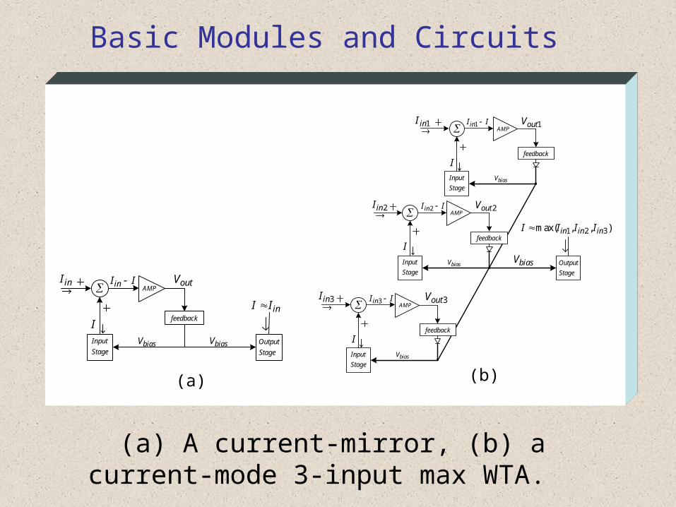
(a) A current-mirror, (b) a current-mode 3-input max WTA.
Basic Modules and Circuits
2inI 2outV
biasV
Stage
Input
Stage
OutputbiasV
),,max( 321 ininin IIII
IIin 2
1inI
I
1outV
biasV
Stage
Input
feedback
IIin 1
3inI 3outV
biasV
Stage
Input
IIin 3
feedback
feedback
AMP
AMP
AMP
I
I
inI outV
biasVStage
Input
Stage
Output
feedbackinII
IIin
biasV
AMP
I
(a) (b)

1:1
II Signout 1
II in
1:1Sign
AnalogSwitch
AnalogSwitch
1:1Sign
ASTR module
Basic Modules and Circuits
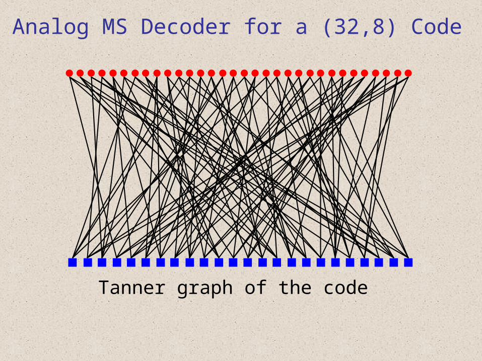
Analog MS Decoder for a (32,8) Code
1 2 3 4 5 6 7 8 9 10 11 12 13 14 15 16 17 18 19 20 21 22 23 24 25 26 27 28 29 30 31 32
1 2 3 4 5 6 7 8 9 10 11 12 13 14 15 16 17 18 19 20 21 22 23 24
Tanner graph of the code

Architecture of the implemented chip
memory
chipon
bits
632
32
bit5
DAC
&
ASTR
Modules
32
Variable
Nodes
24
CheckParity
Nodes
96
logAna
Switches
MUX
Output 1:32
bits5
Address
Databits6
Analog MS Decoder for a (32,8) Code

Microphotograph of the fabricated chip
Analog MS Decoder for a (32,8) Code

16/21
Measurement Results

Measurement Results

Measurement Results
Technology Throughput(Mb/s)
Core(mm2)
Power(mW)
Supply(V)
Transistors Power/speed
Code
Lustenbergeret al.
0.8µmBiCMOS
100 2.89 50 5 BJT ( 940)
p-MOS (650)
0.5 nJ/b
(18,9,5) tailbiting
Moerz et al. 0.25µmBiCMOS
320 0.12 20 3.3 BJT ( 441)
n-MOS (356)
0.06nJ/b
(16,8,3) tailbiting
Gaudet et al. 0.35µmCMOS
(subthreshold)
13.3 1.32 185 3.3 CMOS 13.9nJ/b
Turbo Code (length 16)
Winsteadet al.
0.5µmCMOS
(subthreshold)
2(0.02)
0.82 1(0.016)
3.3 CMOS 0.5 nJ/b(0.8nJ/b)
(8,4,4)
Amat et al. 0.35µmCMOS
(subthreshold)
2 4.1 10.3 3.3 CMOS(26,000)
5.2nJ/b
Turbo Code (length 40)
This work 0.18µmCMOS
24 0.57 5 1.8 CMOS (18,800)
0.2nJ/b
(32,8,10) Code

Conclusion
A modular methodology was proposed for designing CMOS analog MS iterative decoders.
The modules are based on current mirrors and therefore our approach can be used for implementing analog MS decoders in advanced bipolar and CMOS technologies.
A proof-of-concept analog MS decoder chip for a (32,8) regular LDPC code was fabricated and tested.
In low-SNR region, measurement results are close to the simulation results based on SR-MS algorithm.