a high- power dc- dc converter for high.pdf
TRANSCRIPT
7/30/2019 A High- Power DC- DC Converter for High.pdf
http://slidepdf.com/reader/full/a-high-power-dc-dc-converter-for-highpdf 1/9
1 9 9 8 年 12 月 北 方 交 通 大 学
学 报 Dec. 1 998
第 22卷第 6期 JOUR NA L OF NOR TH ER N JIAOT ON G U NIVER SIT Y Vol . 2 2 N o. 6
A High- Power DC-DC Converter for High
Frequency High- Input Voltage Using IGBT*
P eng Guan gfeng H ao R on gtai ( Co ll ege of M echanica l and Elect rical Eng ineering, North ern Jia otong U niv ersity, Beijing 100044)
Solar inverters Abstract F or th e h ig h f requen cy and h igh- inp ut- volt ag e ( somet im es reach in g several
kilo- volt s) con vert er, it s sw itch ing devices - IGBT s volt age rating can n ot su it t h is re-
qu irement . In th is paper, a new cascaded - inverter - un it s stru ctu re is proposed, in w hich
th e h igh- input-volt age is div ided int o several part s an d each part corresponds t o one DC-
A C converter. S o th e IGBT s operating volt ages are equal to t he volt ag e of each d ivided
part . In order to in crease t he out put pow er, th e ou tpu t- rect if ier - diodes usu ally are used
in parallel, a method t o b alan ce th e cu rrent by changing t h e lin k in g ty pe betw een t he
tran sformer secon dary win din gs and t he out put- rectifier diod es is recommen ded . T his
met hod fully u tilizes t he t ransf ormer leakage indu ctance to realize th e curren t- sharin g
f un ct ion. In t his paper, o perat ion of a h ig h- in put volt age, h ig h- pow er D C- DC con verter
is described . Bot h ex per iment al an d simulat ion results are show n for a s mal-l f u l-l s cale-
mod el converter.
Key words high- inpu t- voltage h ig h- frequency IGBT DC-DC converter
大功率高压输入的 IGBT 高频直-
直变换器
彭光凤 郝荣泰 (北方交通大学机械与电气工程学院, 北京 100044)
摘 要 在高频高压输入的情况下, 开关器件 绝缘门极双极晶体管( IG BT )的耐压 不能满 足要求.
文中论述了一种逆变单元串联的结构, 它将输 入的高电压 分成几部分,每一 部分有一 个 DC-A C逆
变器. 此时, IGBT 的工作电压等 于各 部分电压. 为了 提高输 出功率,输 出整 流二 极管 通常 并联 连
接, 变压器的副边漏电感作为二极管的均流电 感.并分 析了高压 输入的大功 率 DC- DC 逆变器的 工
作情况,同时给出了模拟结果和实验结果.
关键词 高压输入 高频逆变 绝缘门极双极晶体管 直- 直变
换器
分类号 T M 46
4
In the elect r omot ive, metros, t rolleys etc. , high- voltage f eed is usually used. Generally, the

7/30/2019 A High- Power DC- DC Converter for High.pdf
http://slidepdf.com/reader/full/a-high-power-dc-dc-converter-for-highpdf 2/9
* 国家自然科学基金资助项目 本文收到日期 1998- 09-13 彭光凤 女 1972 年生 硕士生 email bf xb@ c enter. njtu. edu. cn

7/30/2019 A High- Power DC- DC Converter for High.pdf
http://slidepdf.com/reader/full/a-high-power-dc-dc-converter-for-highpdf 3/9
7/30/2019 A High- Power DC- DC Converter for High.pdf
http://slidepdf.com/reader/full/a-high-power-dc-dc-converter-for-highpdf 4/9
北 方 交 通 大 学 学 报7 6
h igh- volt age sh ou ld be changed int o t he suitable low volt age. It is f ound t h at t h e low-f requency ,
high- pow er t ran sformers are bu lk y, it could not meet th e requ irement s of th e assist ant power
source.
In order to solve th is p r o b lem, it needs to use the high- f requ ency con verter, but the high- f re-
quency pow er swit ch in g device voltage rat in g is usually low , could n ot meet t he need of th e h igh-
in put voltage. For pow er levels up t o t ens of k V A , IGBT s are economical. Generally a cascaded
devices st ruct ure can improve t he convert er s o perat in g volt age, but t he d evice n eeds voltage-
shar -
ing circuit w hich influences th e con verter s outp ut volt age waveforms and lim it s it s h ig hest f re-
quency, So t his method does not suit the s ituations above.
F or t he h igh- in put volt age, h igh- f requency , high- pow er DC- D C con verter, a more at t ract ive
app roach is t he cascaded - inverter - un it s structu re, w hich can redu ce sw itching d evices applied
volt age to its volt ag e- rat ing range and yet does not in fluence th e converter s oth er characters at t he
same t ime. In t h is st ru cture each invert er u nit h as an in put stage voltage- sharin g capacit or and an
ou tpu t volt aic- isolat in g tran sformer wh ile all t he transformer s secon dary w ind ing s are con nected
toget her. Wh en t he out put voltage is low and t he ou tp ut power is h igh , such as h und reds of volt
and t ens of k V A, t he h igh-
f requency rect ifier diodes curren t-
sharin g in ductance, curren t-
sharin gof these parallel diodes is solved by u sing t he t ran sformers leak age indu ctances.
T he sn ubber circuit of IGBT , the h ig h f requency converters w it h IGBT , desig n on output
transformer and th e g at e- drive requirement s of IGBT are in troduced respectively in th ese ref er -
ences as[ 1, 2]
.
T his aim of th is paper is t o design an o pt im um con verter s st ruct ure wit h high- out put power
u nder h ig h- in put voltage. First a brief analysis of th e convert er s t opology is present ed, t hen t he
o perat ing process of t he w hole syst em , t he calculat ion f or mu las of t he voltage- sharin g cap acitor s
paramet er, th e s imu lation an d ex p erient ial results to verify th e converter s design is p resen ted
too.
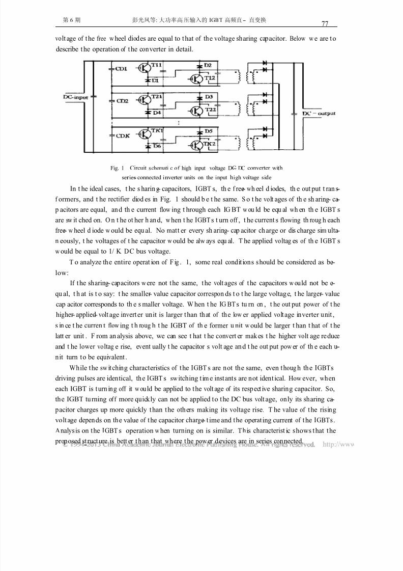
1 The Conver ter 's To pology
T he t opology of t he h igh f requ ency and high inpu t volt age DC-DC converter in w h ich t he K
hy b rid inverters are series con nected w hile K - high f requ ency A C linking b y isolat ing t ransf ormers
is s how n in Fig. 1. T h e IGBT modules are employed to const ruct th e converter s sw it ches. Be-
cause of th e high sw it ch in g sp eed an d low con duction voltage drop of t he IGBT modules, its con-
vers ion loss is low and th e system ef ficiency is h ig h. It is k now n t hat if a volt age- sh aring capacitor
is in p arallel w ith an in verter un it t hen th e volt age of th e capacitor is t h e o perat in g voltage of t he
in verter u nit. H ere t he invert er unit is composed of t wo IGBT s and t wo f ree w heel d iodes; here
th e ad vant age of th is s tructure is t h at th ere is no D C st age short. H owever th e d uty rat io must beless t h an 50% , so t he tran sformers ut ilizat ion factor is low er. It is f oun d t hat if th e DC short
pr otection is ef fective, the bridge converter can be used [ 2]
, so that the system eff iciency w ould be
im p roved. A ll th e IGBT s in Fig. 1 sh ou ld be of fered t he gate- d riving pulse simu ltaneously. It is
found that the max imum applied forw ard volt age of t he IG BTs and the maximum applied reverse
7/30/2019 A High- Power DC- DC Converter for High.pdf
http://slidepdf.com/reader/full/a-high-power-dc-dc-converter-for-highpdf 5/9
第 6 期 彭光凤等:大功率高压输入的 IGBT 高频直- 直变换77
volt age of the free w heel diod es are equal to that of the voltage sharing capacitor. Below w e are to
describe the operation of the converter in detail.
Fig. 1 Circuit schemati c of high input voltage DC- DC converter with
ser ies- connected i nverter units on the input high voltage s id e
In t he ideal cases, t he s harin g- capacitors, IGBT s, th e f ree- wh eel d iodes, th e out put t ran s-
f ormers, and t he rectifier diod es in Fig. 1 should b e t he same. S o t he volt ages of th e sh aring-
ca- p acitors are equal, and th e current flow ing t hrough each IG BT w ou ld be equ al wh en th e IGBT s
are sw it ched on. O n t he ot her h and, w hen t he IGBTs t urn off , t he current s flowing th r oug h each
f ree- w heel d iode w ould be equ al. No matt er every sh aring- cap acitor charge or dis charge sim ulta-
n eously, t he voltages of t he capacitor w ould be alw ays equ al. T he applied voltag es of th e IGBT s
w ould be equal to 1/ K DC bus voltage.
T o analyze the entire o perat ion of F ig . 1, some real cond it ions should be considered as be-
low:
If the sh aring- capacitors w ere not the same, the volt ages of the capacitors w ou ld not be e-
qu al, t h at is t o say: t he smaller - value capacitor correspon ds t o t he large voltage, t he lar ger - value
cap acitor corresponds to th e s maller voltage. W hen t he IG BTs tu rn on , t he out put power of t he
higher - applied - volt age inverter un it is larger than that of the low er applied voltage inverter u nit ,
s in ce t he curren t flow ing t h r oug h t he IGBT of th e former u nit w ould be larger t han t hat of t he
latt er unit . F rom an alysis above, we can see t hat t he convert er mak es t he higher volt age reduce
and t he lower voltag e rise, event ually t he capacitor s volt age and t he out put pow er of th e each u-
n it turn to be equ ivalent .
W h ile the sw it ch ing characteristics of the IGBT s are not the same, even t houg h the IGBTs driving pulses are iden tical, the IGBT s sw itching t im e inst ants are not iden t ical. How ever, when
each IGBT is t urn ing off it w ou ld be applied to the volt age of its resp ect ive sharing capacitor. So,
th e IGBT tu rning of f more qu ick ly can not be applied to the DC bus volt age, on ly its sharing ca- pacitor charges up more quickly than the others mak ing its voltage rise. T he value of the ris ing
volt age depends on the value of the capacitor ch ar ge- t ime and the operating current of the IGBT s .
A nalys is on the IGBT s operation w hen turning on is similar. T h is ch aracterist ic shows that the
pr o posed st ructure is bett er t han that where the pow er d evices are in series connected.
7/30/2019 A High- Power DC- DC Converter for High.pdf
http://slidepdf.com/reader/full/a-high-power-dc-dc-converter-for-highpdf 6/9
北 方 交 通 大 学 学 报7 8
If th e con duction volt age- drops of t he IGBT s in F ig . 1 are not t he same and t he initial volt-
age of t he sh aring- capacit ors are equ al, th e ou tpu t powers of every invierter un it would not be e-
qu al w hen th e IGBT s are sw it ched on . So t he sh aring cap acitors can n ot char g e or discharge e-
qu ally , t he h igh er voltage corresponds t o t he high er con duct ion voltage- drop. Even tu ally, each
in verter u nit gives t he equal pow er and th e current f low in g t hrough each transformer is t he s ame,
th e differences equal to these of the IG BTs con duct ion voltage-drops.
It is wort h to note that, the operating processes are s imilar w hile the t rans formers, the in it ial
volt ages of the sharing capacitors and the output rectifier d iodes are not the same, and here we do
not analyze them one by one. It is f ound that the considered structure can suit the situations of the
high input st ag e voltage and low power sw itching devices voltage rat ing, the converter can ba-l
ance the condition curren ts and reduce the applied volt ages of the power devices.
Since t he p roposed system considers a high- f requ ency and h ig h- pow er con vert er, th e out put
rect if ier d iodes should b e h ig h-s peed w it h t he large curren t rat ing . Bu t t he high- speed d iodes cu r -
rent rat in g could not suit t he sit uat ion s of th e large ou tpu t current usually. In order to increase t he
ou tpu t power, t he d iodes should be in p arallel, bu t th e assist ant curren t- sharin g inductances can
bring about some disad vant ages such as limit ing the max imum operating frequency, increasing thesw itching sp ik e voltage
[ 3]. Fig. 1 has show n that one transformer has several secondary w ind -
ing s, an d each of t hem is connect ed in series w ith a rectifier diode. Here t he current-sh aring p r o b-
lem is solved b y using t he transformers leakage in duct ances. T he proposed structu re f u nct ions a-
like t hat of cascading an in duct an ce, wit h its resp ect ive diodes in p arallel. Bu t it can overcome t he
disad vant ages men t ioned above.
2 Parameter Com putation
It is t he key issue how to select t he sharin g capacit or, because th e syst em s regulat ing t ime is
mainly in fluenced b y t he value of th e capacit ors . W hen th e pow er device s sw it ch in g speeds are
not ident ical, th e voltage of its respect ive cap acit or s value must b e not too sm all. How ever t he
system is adaptive, it should reach to the balance st atus as quick ly as possib le when some sit ua-
t ion s ment ion ed above occu r, such as d if ference w ith in th e sh aring capacitors, t ran sformers, and
th e init ial volt ages of t he cap acitors etc. it is conclu ded th at t he cap acit or sh ould be as small as
possible.
In add it ion , t he st o ppag e st ates should be considered. For example, w hen on e invert er un it
does n ot o perate and t he ot hers o perate regu larly, th e sh aring capacitor correspond ing to th e b reak
u nit charges up quick ly . In order t o avoid pun ch in g of t he pow er devices, t he sharin g capacitor
must be larger than the m in imum value.
T he value of th e sh aring capacit or is dependent on th e factors men tioned above. N ow weconsider the most d isad vantageous cond it ions.
In case only one pow er d evice is tu rning on and th e ot hers are t urning of f, t he leak age induc-
t ance of th e ou tpu t transformer wou ld be larger. T hen t he value of t he sharin g capacitor sees t he
equation ( 1)
7/30/2019 A High- Power DC- DC Converter for High.pdf
http://slidepdf.com/reader/full/a-high-power-dc-dc-converter-for-highpdf 7/9
第 6 期 彭光凤等:大功率高压输入的 IGBT 高频直- 直变换79
C1 =1 2 ( K - 1)
I 2 t ( 1) U pk K
w h ere K is th e n umber of t he invert er u nits, I 2 th e o perat in g cu rrent of t he pow er device, U pk
th e allow ed rip ple volt age, t t he swit ching- off time g ap b et ween t he f astes t device and t he s low-
est device.
In case only one in verter unit is off, w hile the others are being shorted, the value of the
sh aring capacitor is com puted by the follow ing equat ion ( 2) ,
C 2 =1 K - 1
I s t s ( 2)
Us K
w here K is the number of the inverter un its, I s the short ing current , t s the allowed short ing time,
U s the allow ed ripple voltage. Detailed inf erence of the tw o above equations sees the ref er -
ence[ 4 ]
.
T he maximum of the values of C 1 and C 2 is chosen as the value of the sharing capacitor C d .
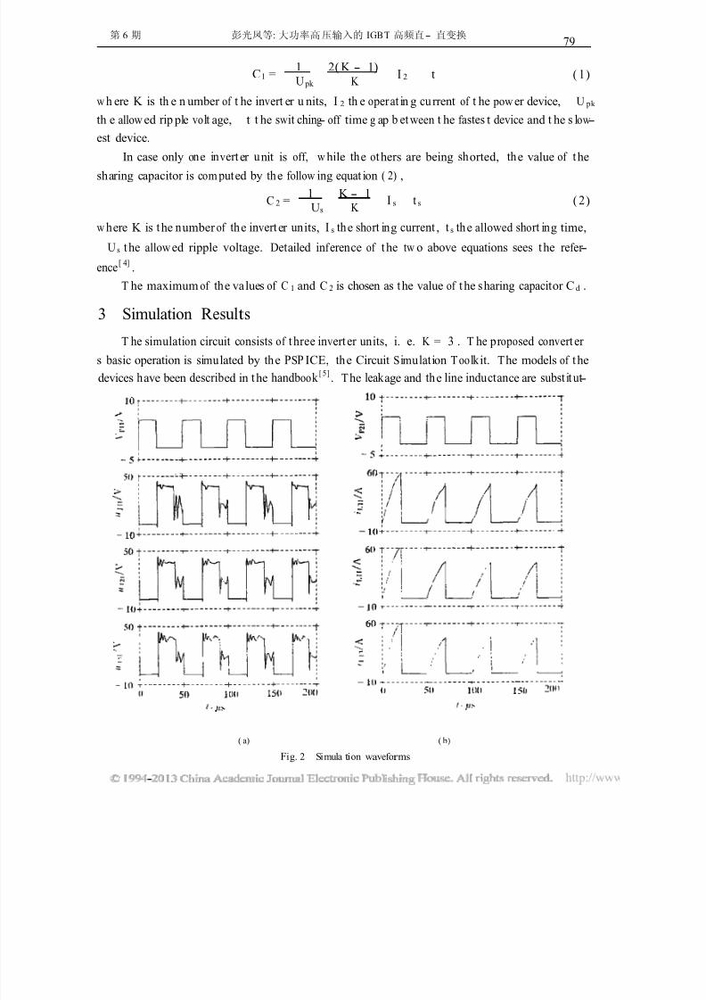
3 Simulation R esults
T he simulation circuit consists of t hree invert er un its, i. e. K = 3 . T he p r o posed convert er s basic operation is simu lated by the PSP ICE, the Circuit S imu lation T oolk it. The models of the
devices have been described in the handbook [ 5 ]
. The leak age and the line indu ct ance are subst it ut-
( a) ( b)
Fig. 2 Simula tion wavefor ms
7/30/2019 A High- Power DC- DC Converter for High.pdf
http://slidepdf.com/reader/full/a-high-power-dc-dc-converter-for-highpdf 8/9
北 方 交 通 大 学 学 报8 0
ed by some lu mped in duct ances. T he s imu lation result s see Fig. 2. F ig. 2 ( a) shows t he applied
volt ages of t he IG BTs, Fig. 2 ( b ) shows t he flow ing cu rrent of th e IGBT s, w hich b elong to t he
different inverter units.
4 Cir cuit Control Str ategies
V arious cont rol schemes shou ld correspond t o various w ays of inp ut ting th e voltage. Wh en
in put t ing a DC voltag e, th e simplest con trol w ay is t o modify th e pu lse-
w idth according to t he
need of t he out put voltage. W hen in put ting an AC volt age, we sh ould rect ify and filter at f irst , b
ut it s is wort h t o n ote t h at th e DC b us also has rippled wh ere t he PWM con trol schem e should be u
sed to mak e th e act ive curren ts of t he IGBT s iden tical during each period. T he w ider pulse cor -
respon ds to t he smaller volt age. A lso t h e f iltering capacit or sh ould be sm aller, t hen t he out pu t DC
volt age can be smoot her [ 3 ]
.
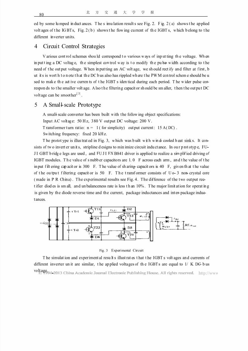
5 A Smal-l scale Pr ototy pe
A smal-l scale converter has been bu ilt w ith the follow ing object specif ications:
Inpu t AC volt ag e: 50 H z, 380 V output DC voltage: 200 V .T ransf ormer turn rat io: n = 1 ( for simplicity) output cu rrent : 15 A ( DC) .
Sw itch ing frequency: fixed 20 kH z.
T he pr otot ype is illus trat ed in Fig. 3, w hich was b uilt w it h w in d - cooled h eat sink s. It con-
sists of tw o invert er un it s, stripline d esigns to min imize circuit indu ctance. In ou r p r ot oty p e, FU-
J I GBT b rid g e legs are used , and FU J I EX B841 driver is applied to realize a sim plif ied driving of
IGBT modules. T h e valu e of s nubb er capacitors are 1. 0 F across each ar m , and t he value of t he
in put f ilt ering cap acit or is 300 F. T he value of sh aring- capacit ors is 40 F, given th at t he value
of t he ou tpu t f ilterin g capacit or is 50 F. T h e t ransf ormer consists of U o- 3 non- crystal core
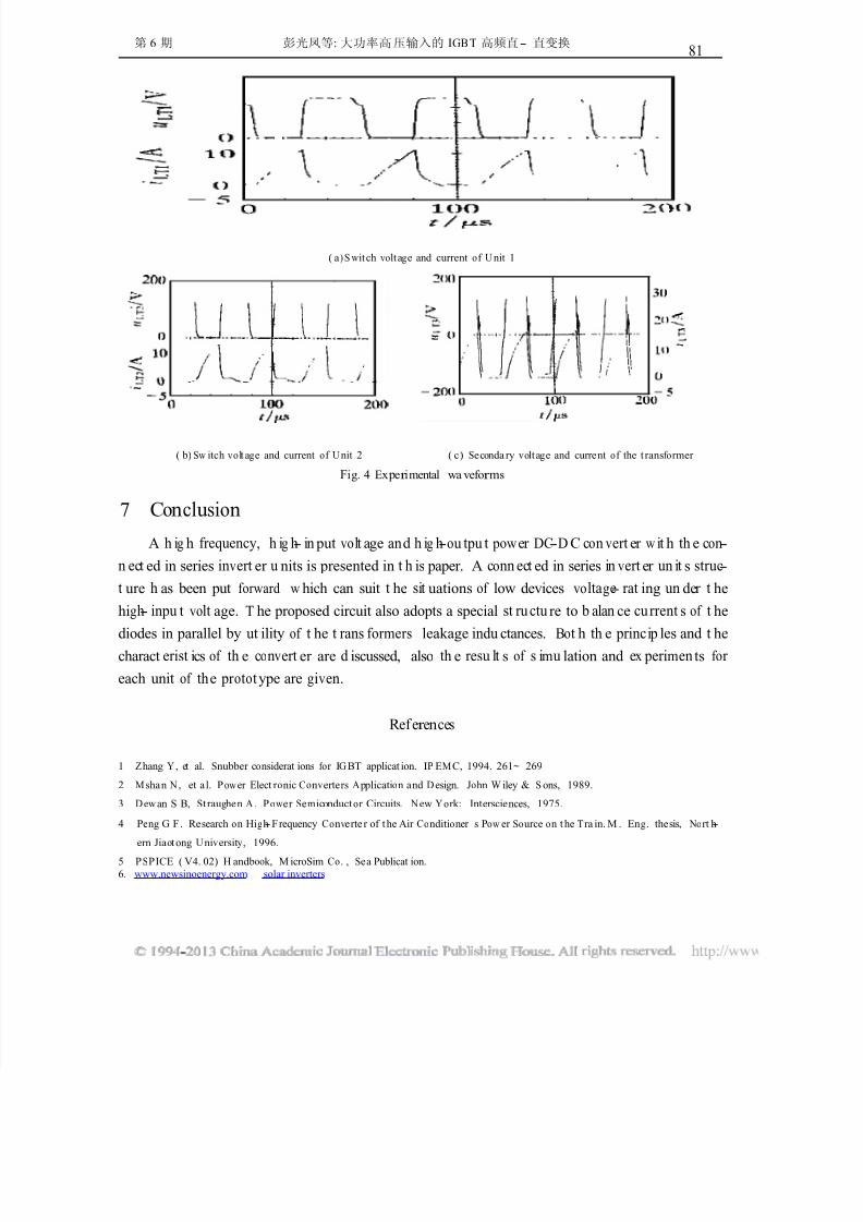
( mad e in P R Ch in a) . T he ex p erimental results see Fig. 4 . T he d if ference of the t wo output rec-
t ifier diod es is sm all, and un balanceness rate is less t h an 10% . T he major limit at ion for o perat in g
is given by the diode reverse time and the curren t, package inductances and int er -package induc-
t ances.
Fig. 3 Ex per imental Cir cui t
T he simulat ion and ex periment al resu lt s illust rat es t hat t he IGBT s volt ages and currents of
different inverter un it are similar, t he ap plied voltages of th e IGBT s are equal to 1/ K DC- b us
volt age.
7/30/2019 A High- Power DC- DC Converter for High.pdf
http://slidepdf.com/reader/full/a-high-power-dc-dc-converter-for-highpdf 9/9
第 6 期 彭光凤等:大功率高压输入的 IGBT 高频直- 直变换81
( a ) S witch vo lt age and current of Unit 1
( b) Sw itch v o lt age and current of Unit 2 ( c) Se conda ry v olt age and current of the t ransf ormer
Fig. 4 Ex per imental wa vefor ms
7 Conclusion
A h ig h frequency, h ig h- in put volt age and h ig h-ou tpu t power DC-D C con vert er w it h th e con-
n ect ed in series invert er u nits is presented in t h is paper. A conn ect ed in series in vert er un it s struc-
t ure h as been put forward w hich can suit t he sit uations of low devices voltage- rat ing un der t he
high- inpu t volt age. T he proposed circuit also adopts a special st ru ctu re to b alan ce cu rrent s of t he
diodes in parallel by ut ility of t he t rans formers leakage indu ctances. Bot h th e princip les and t he
charact erist ics of th e convert er are d iscussed, also th e resu lt s of s imu lation and ex perimen ts f or
each unit of the pr ototype are given.
R efer ences
1 Zhang Y , et al. Snubber considerat ions f or IGBT applicat ion. IP EMC, 1994. 261~ 269
2 M shan N , et a l. P ower Elect r onic Co nv erters A pplica tion and Design. John W iley & S ons, 1989.
3 D ewan S B, St ra ughen A . P o wer Se miconduct or Circuits. New Y ork: Int ersciences, 1975.
4 Peng G F . Research on Hig h- Frequency Co nve rte r of the Air Co nditioner s Po w er Source on the T ra in. M . Eng. thesis, No rt h-
ern Jia otong U niv ersity, 1996.
5 P SPICE ( V4. 02) H andbook, M icroSim Co. , Sea Publicat ion.
6. www.newsinoenergy.com solar inverters