a generalized approach to determine the switching lifetime
TRANSCRIPT
A Generalized Approach to Determine the Switching
Lifetime of a GaN FET
Sandeep R. Bahl, Francisco Baltazar and Yong Xie High Voltage Power, Texas Instruments Incorporated
2900 Semiconductor Dr., Santa Clara, CA 95051
12500 TI Blvd, Dallas TX 75243, USA
Abstract— The determination of switching lifetime for GaN
products is a very timely and important topic, both for the
assurance of reliable operation in application, and for the
development of standardized industry approaches. The
challenges faced are the complexity of the switching transition,
the dependence of the stress on the application circuit, and the
lack of a broad modeling approach. These have prevented the
realization of a “develop once, use broadly” methodology. We
show, for the first time, an approach that addresses these issues
and results in a generalized methodology to determine
switching stress and calculate lifetime. The model created
directly uses the fundamental stressors of voltage, current and
time from the switching waveform. Using this approach, TI
GaN product is shown to be highly reliable under application-
use conditions.
Index Terms— gallium nitride, lifetime estimation, modeling,
reliability, switching converters
I. INTRODUCTION
GaN devices are important for power management applications due to their higher efficiency and ability to shrink the size of power supplies. They are now being adopted for a wide range of applications from telecommunications, servers, motor drives, laptop adapters and on-board chargers for electric vehicles. For the successful widespread adoption of any technology, it is important to be assured of reliability under application-use conditions.
Power FETs are switched in power management applications, therefore the device lifetime needs to be assured for switching operation. Traditional qualification testing does not consider the switching conditions of power management [1]. For silicon FETs, confidence in the qualification methodology has been built over the years. This is because the long-standing experience has resulted in a detailed understanding of failure modes, the device design knowledge to avoid them, and the development of proxy tests e.g. substrate current monitoring for Hot-Carrier Injection (HCI) robustness [2] and Unclamped Inductive Switching (UIS) testing [3]. These silicon tests, however, have not been shown applicable for GaN FETs due to their different properties. For example, the HCI test needs a body contact, and the UIS test needs avalanche robustness. Lateral GaN FET architectures in current use do not have a suitable body contact. They also do not have avalanche capability, but have transient overvoltage capability instead [4].
The GaN industry has been reporting application-relevant reliability results of GaN FETs through two types of tests. The first involves the determination of switching lifetime
using Accelerated Lifetime Testing (ALT). Devices are typically stress-tested to failure in a simple test-vehicle circuit suitable for applying highly accelerated stress. This approach allows the calculation of lifetime by plotting the failure distributions and obtaining wearout models [5]-[7]. The second type of test involves running the devices in an application circuit [8]-[11]. Application or product circuits are generally more complex and typically not designed for high acceleration, so this test is typically not run till wearout. This type of DHTOL (Dynamic High-Temperature Operating Life) test validates robustness to interactions with other components and other operating modes experienced during product operation. Together, the two types of tests assure that the GaN FET has the desired switching lifetime and runs reliably in application.
II. BACKGROUND
There are three key aspects for the determination of switching lifetime. First, the switching operation is complex, with multiple factors describing the behavior. For example, both voltage and current vary with a corresponding slew rate during the transition. Switching transitions also occur at a certain frequency with the device at a given junction temperature. There are also turn-on and turn-off transitions. Additionally, the on/off ratio of the device while switching is determined by the duty cycle. Running a DOE (Design of Experiments) with all factors is impractical. Second, the device stress depends upon the application circuit, of which are many types. Further, application boards are typically not suited for high acceleration due to thermal constraints and the limitations of other components. They may produce false failures or incorrectly accelerate the failure mode desired. Third, there needs to be a broadly-applicable modeling approach. A desirable outcome, as shown in Fig. 1 is that a test-vehicle circuit suitable for accelerated stress be used to make a model applicable to a broad range of product-level circuits and use-conditions.
Fig. 1: It is highly desirable to develop a broad modeling approach where a
test-vehicle circuit suitable for high acceleration may be used.
Presented at the IEEE International Reliability Physics Symposium (IRPS), Apr. 2020.
© 2020 IEEE. Personal use of this material is permitted. Permission from IEEE must be obtained for all other uses, in any current or future media, including
reprinting/republishing this material for advertising or promotional purposes, creating new collective works, for resale or redistribution to servers or lists, or reuse of any copyrighted component of this work in other works.

These aspects need to be addressed to make progress on the topic of switching reliability. The set of stressors needs to be reduced, for example by considering the ones shown to be important, and by making knowledge-based choices for the others. The importance of voltage, current, and temperature has already been shown [5]-[7]. There is some literature to guide about the role of the other factors. For example, a lower duty cycle would increase charge trapping by increasing the voltage blocking time with respect to on-state time [12], [13]. A higher frequency would result in faster accumulation of switching stress [5], whereas a lower slew rate would result in more hot-electron effects [14], [15] due to an increased I-V overlap. A low duty cycle and reduced slew-rate would therefore provide relevant stress coverage for a wide range of use-conditions.
A test-vehicle circuit may be used to apply accelerated stress if it exercises the same failure mechanism in the FET as the product-circuit would. The use of a test-vehicle circuit is in accordance with JEDEC standard JESD94B [16], which states “A test vehicle may be preferable since the actual product complexity may mask intrinsic failure mechanisms”. The relevance of the stress may be assessed by use of the switching locus curve. The curve shows the trajectory of the drain-current vs drain-voltage waveform for a switching cycle. Its trajectory gives information about the type of switching stress applied to the device. For example, the turn-on hard-switching transition shown by the locus curves in [1], [5] generates hot-electron switching-stress in the channel, which can increase dynamic RDS(ON) [14], [15]. The accumulation of this stress over time can also result in wearout from hard-failure [5]. Relevant accelerated stress may thereby be applied by a test-vehicle circuit with the same type of switching locus curve as that of the intended application [1]. This enables broad application coverage because the same type of switching locus curve represents the stress applied to the device by a broad application class.
The modeling approach also needs to be suited to switching-transition behavior. Present modeling approaches use parametrized stressor values. This is because the model equations used need fixed values. For example, the power-supply voltage and the peak switching current may be chosen to represent a given switching transient. A parametrized approach, however, does not lend itself easily to generalization. For example, a model generated using a test-vehicle at reduced slew rate may not be applicable to an application circuit running at higher slew rate, where larger peak currents but shorter switching durations result. Such a model may also not be applicable to circuit topologies that differ from those used to conduct the stress test.
III. DESCRIPTION OF THE APPROACH
This work demonstrates the use of a test-vehicle stress circuit to generate a broadly applicable switching lifetime model. It also simplifies DOE complexity and stressor parametrization aspects by directly utilizing the switching waveform. The switching waveform captures the complexity of the switching transition, and directly contains the voltage, current and slew rate information.
Our approach builds upon the finding of Ikoshi et al. [5] that the wearout from switching stress accumulates till failure
occurs. This allows a switching transition to be broken into a
series of discrete points and the unit stress values (stress) for each point summed. The concept is shown in Fig. 2. With the assumption of constant voltage and current for each time
point, stress may be represented by:
∆𝑠𝑡𝑟𝑒𝑠𝑠 = 𝑣𝐷𝑆 × 𝐴𝐹𝑉 × 𝑖𝐷 × 𝐴𝐹𝐼 × ∆𝑡𝑖𝑚𝑒 (1)
Where vDS and iD are the instantaneous values of the drain voltage and current respectively, and AF
(V,I) is the respective
acceleration factor. Equation (1) assumes the independence of voltage and current, as was shown by [5]. Interaction-effects, if required, would be treated by including suitable
cross-terms. The stress units are summed in order to calculate the stress per switching transition, 𝜎𝑇𝑟:
𝜎𝑇𝑟 = ∑ ∆𝑠𝑡𝑟𝑒𝑠𝑠(𝑡𝑡 (𝑒𝑛𝑑)
𝑡 (𝑠𝑡𝑎𝑟𝑡)) (2)
The concept of using the overlap sum or integral of the voltage and current waveforms is already well-known for the calculation of switching loss, e.g. as used in [17]. It is more relevant to use the channel current in Eq. (1), however. Use of the channel current is physically based, since hot channel electrons have been shown to be a stimulus for dynamic Rds-on increase [15]. The overlap integral of the drain voltage and channel current has also been shown to explain the observed increase in dynamic RDS(ON) [14] during device hard-switching turn-on. The channel current, ICh, may be calculated by assuming that the displacement current from the output capacitance, COSS, flows through the channel.
𝐼𝐶ℎ = 𝑖𝐷 + 𝐶𝑜𝑠𝑠(𝑣𝐷𝑆) ×𝑑𝑣𝐷𝑆
𝑑𝑡 (3)
We define the switching stress rate, SSW, as the transition stress with acceleration factors applied for the other stressors and a constant, C, for normalization to units of hour and kHz.
𝑆𝑆𝑊 = [𝐶 × 𝜎𝑇𝑟 × 𝐴𝐹(𝑇) × 𝐴𝐹(𝐷)] × 𝐴𝐹(𝑓𝑆𝑊) (4)
Where T is the temperature in Kelvins, fsw is the switching frequency in kHz and D is the duty cycle. This manner of incorporating the non-transient stressors allows the use of any model function. The quantity in square brackets is the switching stress applied to the device per hour when switching at 1 kHz. This quantity may be used for the x-axis of a failure distribution plot. Its use to represent switching
Fig. 2: A switching waveform can be broken into the fundamental
components of voltage and current stress applied to the device. This allows for a basic-principles calculation of switching stress by discretizing the
waveform and summing the unit stresses

stress is analogous to the use of “time” in a DC stress, to represent a constant rate of stress. It is assumed that the accelerated-stress conditions are chosen such that the maximum stress is from the switching transitions. The inverse of SSW is the time to failure (TTF):
𝑇𝑇𝐹 = 1 ⁄ 𝑆𝑆𝑊 (5)
Where TTF is the lifetime at a given failure fraction (e.g. MTTF or other specified fraction) chosen for which the model parameters are fitted.
The model functions chosen are well-regarded acceleration equations of semiconductor physics and were selected using a best-practice approach from both JEDEC documents and prior art [5], [18], [19]. Exponential functions were chosen for both voltage and current, and an Arrhenius dependence chosen for temperature. An additional power-law function was chosen for the current due to its relevance in modeling hot-carrier degradation [18]. The final model was based upon the function giving the most conservative (lowest) lifetime. A power-law function was chosen for the frequency to account for the cumulative nature of switching stress. The functions used are shown in Fig. 3.
The stress-test vehicle used is based upon the familiar double-pulse tester (DPT). It provides the device with hard-switching stress, as seen from the switching locus plot of Fig. 4. We use the DPT in continuous-pulse mode for providing repetitive accelerated hard-switching stress. Its simplicity minimizes system-related failures. A high-reliability SiC Schottky diode is used for the high-side device, eliminating high-side device failures and drive issues like Common Mode Transient Immunity (CMTI) or unintended shoot-through. The stress-test does not consume much energy and the GaN FET remains at the desired temperature, which is important for running multiple units. It uses a low duty cycle, which provides further acceleration due to the higher ratio of blocking time vs. on-state time. The schematic of the test vehicle is shown in Fig. 1 as a boost converter with the output current re-circulated to the input.
IV. DATA AND MODEL.
A DOE was run to determine the effects of voltage,
current, temperature and frequency, as shown in Fig. 5. A
slew-rate of 50 V/ns and switching frequencies between 12
kHz and 50 kHz were used. The reduced (~midrange) slew-
rate provides higher hot-electron stress (larger switching
loss). The switching waveforms of the voltage and current
were carefully captured and de-skewed to be representative
of the stress stimuli applied at the device terminals.
The switching-locus plot of the baseline (640 V) turn-on transition is shown in Fig. 4. The figure shows both the drain and channel currents. The shape shows a hard-switching trajectory. The channel current was calculated using Eq. (3), and the locus shows channel current flow at high drain-source voltage. Fig. 4 also shows a schematic illustrating the calculation. Accelerated hard-switching stress was applied to the devices until hard-failure. The Weibull plots are shown in Fig. 6. The five legs of the DOE were simultaneously fitted to the same slope, as would occur by accelerating the same failure mechanism. The stress time was normalized by the experimentally-determined frequency scaling factor using the frequency scaling function shown in Fig. 3. Note that the Weibull fits of the two frequency DOE legs overlay, since the x-axis represents a normalized switching stress rate.
Experimental switching waveforms were captured for all
the DOE conditions, and the switching stress rate calculation
implemented per equations (1)-(5). The experimental mean
times to failure (MTTF) were determined from the Weibull
parameters [20] of Fig. 6, and the coefficients of the
acceleration equations of Fig. 3 fitted to the failure times of
the respective DOE legs.
Fig. 3: Model functions used in the present study. Stressors were fitted to Arrhenius and exponential models respectively. A power-law model was
also considered for the current dependence, due to its relevance. ICh is the
channel current per Eq. (3).
Fig. 4: The switching locus plot of the hard-switching turn-on transition,
showing both the drain and channel currents. The figure also shows a schematic illustrating the calculation of ICh
Fig. 5: Four-factor DOE, to independently vary voltage, current, temperature and frequency. The values in the boxes are the stress
conditions. The extracted model factors from the DOE are also summarized

Two models were fitted, since there are two appropriate
current-acceleration functions. An Arrhenius dependence was
used for the temperature. The coefficients are summarized in
Fig. 5. The mean times to failure (MTTF) of the
experimentally-determined vs. model-calculated values are
plotted in Fig. 7, showing the excellent fit for both models.
Since each point involves integration over a range of voltage
and current values using the same coefficients, the goodness
of fit indicates the validity of the approach to generate the
value of the switching stress rate.
The model can calculate the switching hard-failure lifetime
of the device in either the test vehicle, or in-application using
both measured and simulated switching waveforms. Fig. 8
shows the calculated lifetime corresponding to measured
waveforms from the test-vehicle circuit and simulated
waveforms from a boost converter. The supply voltage and
inductor current are labeled, and the lifetime calculation is for
the case of all switching transitions occurring at those values.
The exponential model for current acceleration was used,
since it was more conservative (lower lifetime). The model is
also based upon low-duty cycle switching-stress, which is
conservative due to a higher overall duration at high voltage.
The MTTF, for example, of the LMG3410R070 (70 m)
running in a boost converter at 100 kHz, 125°C with IL=8 A
at turn-on and Vds=400 V is 6.9 x10⁹ years.
V. PRODUCT LIFETIME
If the device operates under constant current, the calculation used for the data in Fig. 8 would estimate the product lifetime. However in reality the load current is variable over time. For example, in a PFC (Power Factor Correction) circuit (Fig. 9), the load current varies sinusoidally with the line cycle. The load may also vary over time depending on the line input and/or demand. Further, in the bridgeless totem-pole circuit of Fig. 9, each GaN FET soft-switches for every alternate line half-cycle, during which time the channel is off.
We illustrate an example calculation for the PFC circuit of Fig. 9 with a LMG3410R070 Integrated GaN FET Power Stage switching at 100 kHz (100 V/ns), with 400 V output, 8 A RMS inductor current in Continuous Conduction Mode (CCM). With 230 V RMS AC line input this current represents an input power of 1.84 kW, a respectable power-
level for a 70 m device-based converter. The switching waveforms were generated by simulating a standard boost converter circuit with a DC voltage input using the LMG3410R070 Integrated GaN FET power stage with 400 V output bus voltage and fixed inductor current. The schematic
Fig. 6: Weibull fits for the four-factor DOE of Fig. 4. The x-axis is
normalized to the switching frequency using the experimentally determined frequency scaling factor
Fig. 7: Correlation of the experimentally determined mean times to failure
vs the model-calculated MTTF. Both exponential and power-law functions for the current were used. The figure shows excellent model fitting.
Fig. 8: Switching lifetime MTTF extrapolation using both measured and
simulated waveforms. The exponential model was used because it was
found to be more conservative (lower lifetime). The slew rate for the simulations was about 100 V/ns.
Fig. 9: A schematic of the bridgeless totem-pole PFC circuit with GaN
switches S1 and S2, used for the product lifetime calculations. The switches
labeled Q1 and Q2 are typically slower Si FETs.
is shown in the inset of Fig. 10. Model coefficients for stress calculations at 125°C were applied to the waveforms.
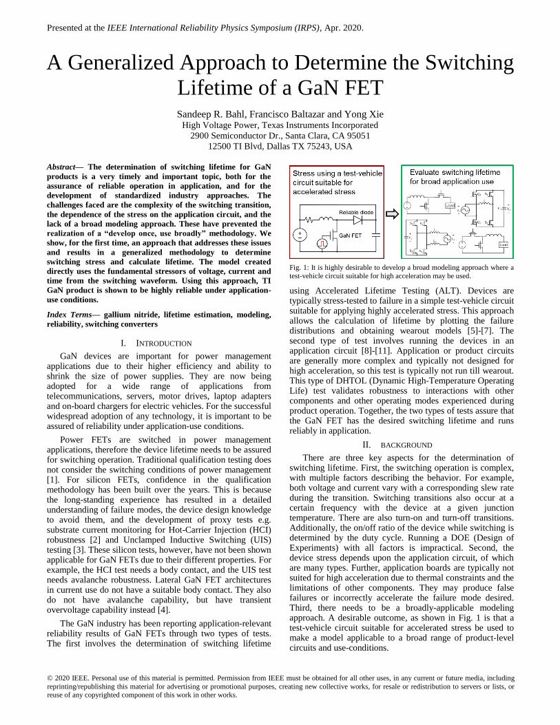
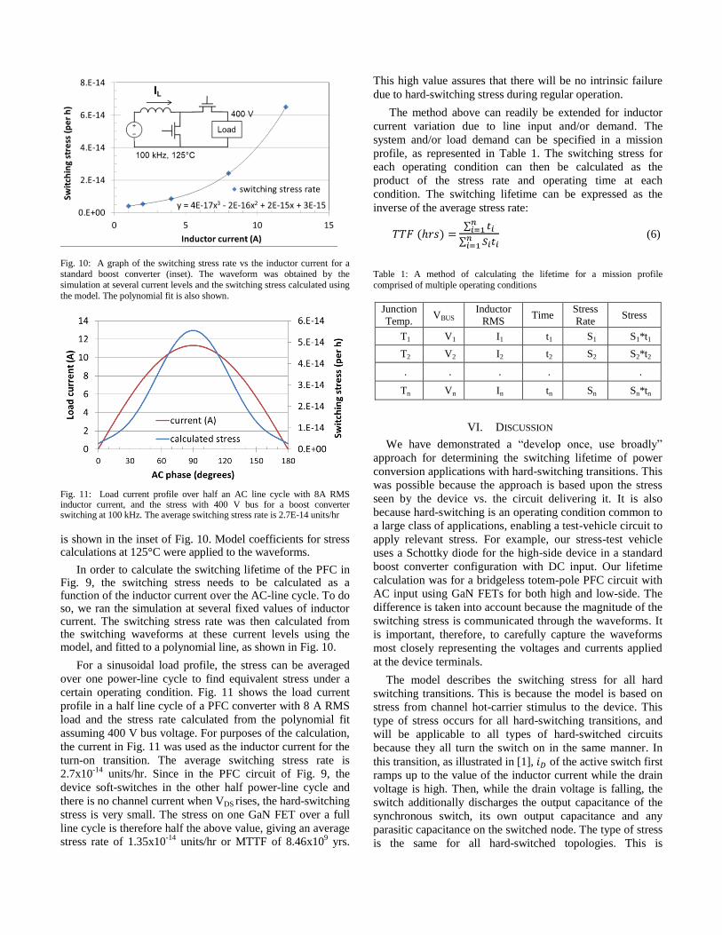
In order to calculate the switching lifetime of the PFC in Fig. 9, the switching stress needs to be calculated as a function of the inductor current over the AC-line cycle. To do so, we ran the simulation at several fixed values of inductor current. The switching stress rate was then calculated from the switching waveforms at these current levels using the model, and fitted to a polynomial line, as shown in Fig. 10.
For a sinusoidal load profile, the stress can be averaged
over one power-line cycle to find equivalent stress under a
certain operating condition. Fig. 11 shows the load current
profile in a half line cycle of a PFC converter with 8 A RMS
load and the stress rate calculated from the polynomial fit
assuming 400 V bus voltage. For purposes of the calculation,
the current in Fig. 11 was used as the inductor current for the
turn-on transition. The average switching stress rate is
2.7x10⁻¹⁴
units/hr. Since in the PFC circuit of Fig. 9, the
device soft-switches in the other half power-line cycle and
there is no channel current when VDS rises, the hard-switching
stress is very small. The stress on one GaN FET over a full
line cycle is therefore half the above value, giving an average
stress rate of 1.35x10⁻¹⁴
units/hr or MTTF of 8.46x10⁹ yrs.
This high value assures that there will be no intrinsic failure
due to hard-switching stress during regular operation.
The method above can readily be extended for inductor
current variation due to line input and/or demand. The
system and/or load demand can be specified in a mission
profile, as represented in Table 1. The switching stress for
each operating condition can then be calculated as the
product of the stress rate and operating time at each
condition. The switching lifetime can be expressed as the
inverse of the average stress rate:
𝑇𝑇𝐹 (ℎ𝑟𝑠) = ∑ 𝑡𝑖
𝑛𝑖=1
∑ 𝑆𝑖𝑡𝑖𝑛𝑖=1
(6)
Table 1: A method of calculating the lifetime for a mission profile
comprised of multiple operating conditions
Junction
Temp. VBUS
Inductor
RMS Time
Stress
Rate Stress
T1 V1 I1 t1 S1 S1*t1
T2 V2 I2 t2 S2 S2*t2
. . . . .
Tn Vn In tn Sn Sn*tn
VI. DISCUSSION
We have demonstrated a “develop once, use broadly”
approach for determining the switching lifetime of power
conversion applications with hard-switching transitions. This
was possible because the approach is based upon the stress
seen by the device vs. the circuit delivering it. It is also
because hard-switching is an operating condition common to
a large class of applications, enabling a test-vehicle circuit to
apply relevant stress. For example, our stress-test vehicle
uses a Schottky diode for the high-side device in a standard
boost converter configuration with DC input. Our lifetime
calculation was for a bridgeless totem-pole PFC circuit with
AC input using GaN FETs for both high and low-side. The
difference is taken into account because the magnitude of the
switching stress is communicated through the waveforms. It
is important, therefore, to carefully capture the waveforms
most closely representing the voltages and currents applied
at the device terminals.
The model describes the switching stress for all hard
switching transitions. This is because the model is based on
stress from channel hot-carrier stimulus to the device. This
type of stress occurs for all hard-switching transitions, and
will be applicable to all types of hard-switched circuits
because they all turn the switch on in the same manner. In
this transition, as illustrated in [1], 𝑖𝐷 of the active switch first
ramps up to the value of the inductor current while the drain
voltage is high. Then, while the drain voltage is falling, the
switch additionally discharges the output capacitance of the
synchronous switch, its own output capacitance and any
parasitic capacitance on the switched node. The type of stress
is the same for all hard-switched topologies. This is
Fig. 10: A graph of the switching stress rate vs the inductor current for a standard boost converter (inset). The waveform was obtained by the
simulation at several current levels and the switching stress calculated using
the model. The polynomial fit is also shown.
Fig. 11: Load current profile over half an AC line cycle with 8A RMS inductor current, and the stress with 400 V bus for a boost converter switching at 100 kHz. The average switching stress rate is 2.7E-14 units/hr
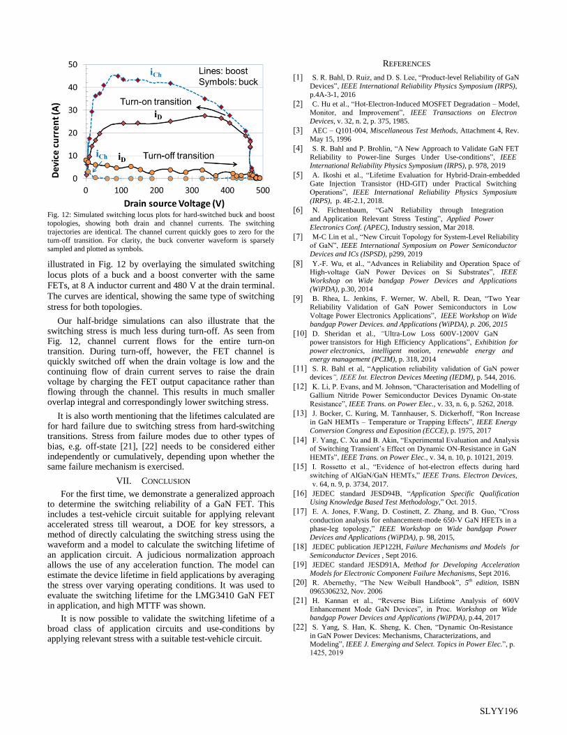
illustrated in Fig. 12 by overlaying the simulated switching
locus plots of a buck and a boost converter with the same
FETs, at 8 A inductor current and 480 V at the drain terminal.
The curves are identical, showing the same type of switching
stress for both topologies.
Our half-bridge simulations can also illustrate that the switching stress is much less during turn-off. As seen from Fig. 12, channel current flows for the entire turn-on transition. During turn-off, however, the FET channel is quickly switched off when the drain voltage is low and the continuing flow of drain current serves to raise the drain voltage by charging the FET output capacitance rather than flowing through the channel. This results in much smaller overlap integral and correspondingly lower switching stress.
It is also worth mentioning that the lifetimes calculated are for hard failure due to switching stress from hard-switching transitions. Stress from failure modes due to other types of bias, e.g. off-state [21], [22] needs to be considered either independently or cumulatively, depending upon whether the same failure mechanism is exercised.
VII. CONCLUSION
For the first time, we demonstrate a generalized approach to determine the switching reliability of a GaN FET. This includes a test-vehicle circuit suitable for applying relevant accelerated stress till wearout, a DOE for key stressors, a method of directly calculating the switching stress using the waveform and a model to calculate the switching lifetime of an application circuit. A judicious normalization approach allows the use of any acceleration function. The model can estimate the device lifetime in field applications by averaging the stress over varying operating conditions. It was used to evaluate the switching lifetime for the LMG3410 GaN FET in application, and high MTTF was shown.
It is now possible to validate the switching lifetime of a broad class of application circuits and use-conditions by applying relevant stress with a suitable test-vehicle circuit.
REFERENCES
[1] S. R. Bahl, D. Ruiz, and D. S. Lee, “Product-level Reliability of GaN Devices”, IEEE International Reliability Physics Symposium (IRPS),
p.4A-3-1, 2016
[2] C. Hu et al., “Hot-Electron-Induced MOSFET Degradation – Model, Monitor, and Improvement”, IEEE Transactions on Electron
Devices, v. 32, n. 2, p. 375, 1985.
[3] AEC – Q101-004, Miscellaneous Test Methods, Attachment 4, Rev. May 15, 1996
[4] S. R. Bahl and P. Brohlin, “A New Approach to Validate GaN FET Reliability to Power-line Surges Under Use-conditions”, IEEE
International Reliability Physics Symposium (IRPS), p. 978, 2019
[5] A. Ikoshi et al., “Lifetime Evaluation for Hybrid-Drain-embedded Gate Injection Transistor (HD-GIT) under Practical Switching
Operations”, IEEE International Reliability Physics Symposium
(IRPS), p. 4E-2.1, 2018.
[6] N. Fichtenbaum, “GaN Reliability through Integration
and Application Relevant Stress Testing”, Applied Power
Electronics Conf. (APEC), Industry session, Mar 2018.
[7] M-C Lin et al., “New Circuit Topology for System-Level Reliability
of GaN”, IEEE International Symposium on Power Semiconductor
Devices and ICs (ISPSD), p299, 2019
[8] Y.-F. Wu, et al., “Advances in Reliability and Operation Space of
High-voltage GaN Power Devices on Si Substrates”, IEEE Workshop on Wide bandgap Power Devices and Applications
(WiPDA), p.30, 2014
[9] B. Rhea, L. Jenkins, F. Werner, W. Abell, R. Dean, “Two Year Reliability Validation of GaN Power Semiconductors in Low
Voltage Power Electronics Applications”, IEEE Workshop on Wide
bandgap Power Devices. and Applications (WiPDA), p. 206, 2015
[10] D. Sheridan et al., “Ultra-Low Loss 600V-1200V GaN
power transistors for High Efficiency Applications”, Exhibition for
power electronics, intelligent motion, renewable energy and
energy management (PCIM), p. 318, 2014
[11] S. R. Bahl et al, “Application reliability validation of GaN power devices”, IEEE Int. Electron Devices Meeting (IEDM), p. 544, 2016.
[12] K. Li, P. Evans, and M. Johnson, “Characterisation and Modelling of Gallium Nitride Power Semiconductor Devices Dynamic On-state
Resistance”, IEEE Trans. on Power Elec., v. 33, n. 6, p. 5262, 2018.
[13] J. Bocker, C. Kuring, M. Tannhauser, S. Dickerhoff, “Ron Increase in GaN HEMTs – Temperature or Trapping Effects”, IEEE Energy
Conversion Congress and Exposition (ECCE), p. 1975, 2017
[14] F. Yang, C. Xu and B. Akin, “Experimental Evaluation and Analysis of Switching Transient’s Effect on Dynamic ON-Resistance in GaN
HEMTs”, IEEE Trans. on Power Elec., v. 34, n. 10, p. 10121, 2019.
[15] I. Rossetto et al., “Evidence of hot-electron effects during hard switching of AlGaN/GaN HEMTs,” IEEE Trans. Electron Devices,
v. 64, n. 9, p. 3734, 2017.
[16] JEDEC standard JESD94B, “Application Specific Qualification Using Knowledge Based Test Methodology,” Oct. 2015.
[17] E. A. Jones, F.Wang, D. Costinett, Z. Zhang, and B. Guo, “Cross conduction analysis for enhancement-mode 650-V GaN HFETs in a phase-leg topology,” IEEE Workshop on Wide bandgap Power Devices and Applications (WiPDA), p. 98, 2015,
[18] JEDEC publication JEP122H, Failure Mechanisms and Models for Semiconductor Devices , Sept 2016.
[19] JEDEC standard JESD91A, Method for Developing Acceleration
Models for Electronic Component Failure Mechanisms, Sept 2016.
[20] R. Abernethy, “The New Weibull Handbook”, 5th edition, ISBN 0965306232, Nov. 2006
[21] H. Kannan et al., “Reverse Bias Lifetime Analysis of 600V
Enhancement Mode GaN Devices”, in Proc. Workshop on Wide bandgap Power Devices and Applications (WiPDA), p.44, 2017
[22] S. Yang, S. Han, K. Sheng, K. Chen, “Dynamic On-Resistance
in GaN Power Devices: Mechanisms, Characterizations, and
Modeling”, IEEE J. Emerging and Select. Topics in Power Elec.”, p.
1425, 2019
Fig. 12: Simulated switching locus plots for hard-switched buck and boost
topologies, showing both drain and channel currents. The switching
trajectories are identical. The channel current quickly goes to zero for the turn-off transition. For clarity, the buck converter waveform is sparsely
sampled and plotted as symbols.
SLYY196

IMPORTANT NOTICE AND DISCLAIMER
TI PROVIDES TECHNICAL AND RELIABILITY DATA (INCLUDING DATASHEETS), DESIGN RESOURCES (INCLUDING REFERENCE DESIGNS), APPLICATION OR OTHER DESIGN ADVICE, WEB TOOLS, SAFETY INFORMATION, AND OTHER RESOURCES “AS IS” AND WITH ALL FAULTS, AND DISCLAIMS ALL WARRANTIES, EXPRESS AND IMPLIED, INCLUDING WITHOUT LIMITATION ANY IMPLIED WARRANTIES OF MERCHANTABILITY, FITNESS FOR A PARTICULAR PURPOSE OR NON-INFRINGEMENT OF THIRD PARTY INTELLECTUAL PROPERTY RIGHTS.These resources are intended for skilled developers designing with TI products. You are solely responsible for (1) selecting the appropriate TI products for your application, (2) designing, validating and testing your application, and (3) ensuring your application meets applicable standards, and any other safety, security, or other requirements. These resources are subject to change without notice. TI grants you permission to use these resources only for development of an application that uses the TI products described in the resource. Other reproduction and display of these resources is prohibited. No license is granted to any other TI intellectual property right or to any third party intellectual property right. TI disclaims responsibility for, and you will fully indemnify TI and its representatives against, any claims, damages, costs, losses, and liabilities arising out of your use of these resources.TI’s products are provided subject to TI’s Terms of Sale (www.ti.com/legal/termsofsale.html) or other applicable terms available either on ti.com or provided in conjunction with such TI products. TI’s provision of these resources does not expand or otherwise alter TI’s applicable warranties or warranty disclaimers for TI products.
Mailing Address: Texas Instruments, Post Office Box 655303, Dallas, Texas 75265Copyright © 2020, Texas Instruments Incorporated