a design methodology for implementation of serial ... · a design methodology for implementation of...
TRANSCRIPT
University of South FloridaScholar Commons
Graduate Theses and Dissertations Graduate School
2005
A design methodology for implementation of serialperipheral interface using VHDLJyothsna KurapatiUniversity of South Florida
Follow this and additional works at: http://scholarcommons.usf.edu/etd
Part of the American Studies Commons
This Thesis is brought to you for free and open access by the Graduate School at Scholar Commons. It has been accepted for inclusion in GraduateTheses and Dissertations by an authorized administrator of Scholar Commons. For more information, please contact [email protected].
Scholar Commons CitationKurapati, Jyothsna, "A design methodology for implementation of serial peripheral interface using VHDL" (2005). Graduate Theses andDissertations.http://scholarcommons.usf.edu/etd/733
A Design Methodology for Implementation of Serial Peripheral Interface Using VHDL
by
Jyothsna Kurapati
A thesis submitted in partial fulfillment of the requirements for the degree of
Master of Electrical Engineering Department of Electrical Engineering
College of Engineering University of South Florida
Major Professor: Wilfrido A. Moreno, Ph.D. James T.Leffew, Ph.D. Sanjukta Bhanja, Ph.D.
Date of Approval: July 17, 2005
Keywords: fpga, protel, spi, mosi, miso, altium
© Copyright 2005 , Jyothsna Kurapati

ACKNOWLEDGMENT
I would like to express my appreciation and gratitude to my major professor, Dr.
Moreno Wilfrido, for the valuable guidance and immense support he provided throughout
the completion of this thesis and my Master’s degree. I would like to express my special
thanks to Dr. Leffew and Dr. Sanjuktha Bhanja for their invaluable support in my course
work.
I am indebted to my parents and my brother for their immense support, inspiration
and faith in me. I would like to express my special thanks to Dr.Deepak Srinivasagupta
and Krishnakanth Barri for their suggestions, support and guidance. I would also like to
express my gratitude to my cousins Divya, Siva, Aravind and Kalpith for their
encouragement, overwhelming support and great friendship. I will forever remain
appreciative of the great company and times their association provided me.
i
TABLE OF CONTENTS
LIST OF TABLES iii
LIST OF FIGURES iv
ABSTRACT vi
CHAPTER 1 INTRODUCTON 1
1.1 In-System Programmability 1
1.1.1 CPLD – MAX 7000S Devices 2
1.1.2 FPGA – FLEX 10K 3
CHAPTER 2 APPLICATIONS OF A SERIAL PERIPHERAL INTERFACE 5
2.1 Robotic Teleoperation 5
2.2 Sensor Bus 6
2.3 Communication Between a Smart Sensor and the Servo Driver 8
CHAPTER 3 INTRODUCTION TO PCB DESIGN USING PROTEL 10
3.1 Rules Driven Layout and Routing 11
3.2 Situs Topological Autorouting 11
3.3 Integrated Mixed Signal Simulation 11
3.4 Pre and Post-Layout Signal Integrity Analysis 11
3.5 Integration of the PCB and FPGA Designs 12
3.6 Complete and Configurable Board-Level Design Environment 12
3.7 Schematic Document of the Circuit 12
3.7.1 MAX 7000S Devices 13
3.8 Printed Circuit Board Design for the Schematic 15
CHAPTER 4 SERIAL PERIPHERAL INTERFACE USING VHDL 20
4.1 SPI Control Register 21

ii
4.1.1 SPE 21
4.1.2 DORD 21
4.1.3 MSTR 21
4.1.4 CPOL 22
4.1.5 CPHA 22
4.1.6 SPR1 22
4.1.7 SPR0 22
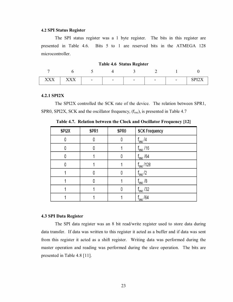
4.2 SPI Status Register 23
4.2.1 SPI2X 23
4.3 SPI Data Register 23
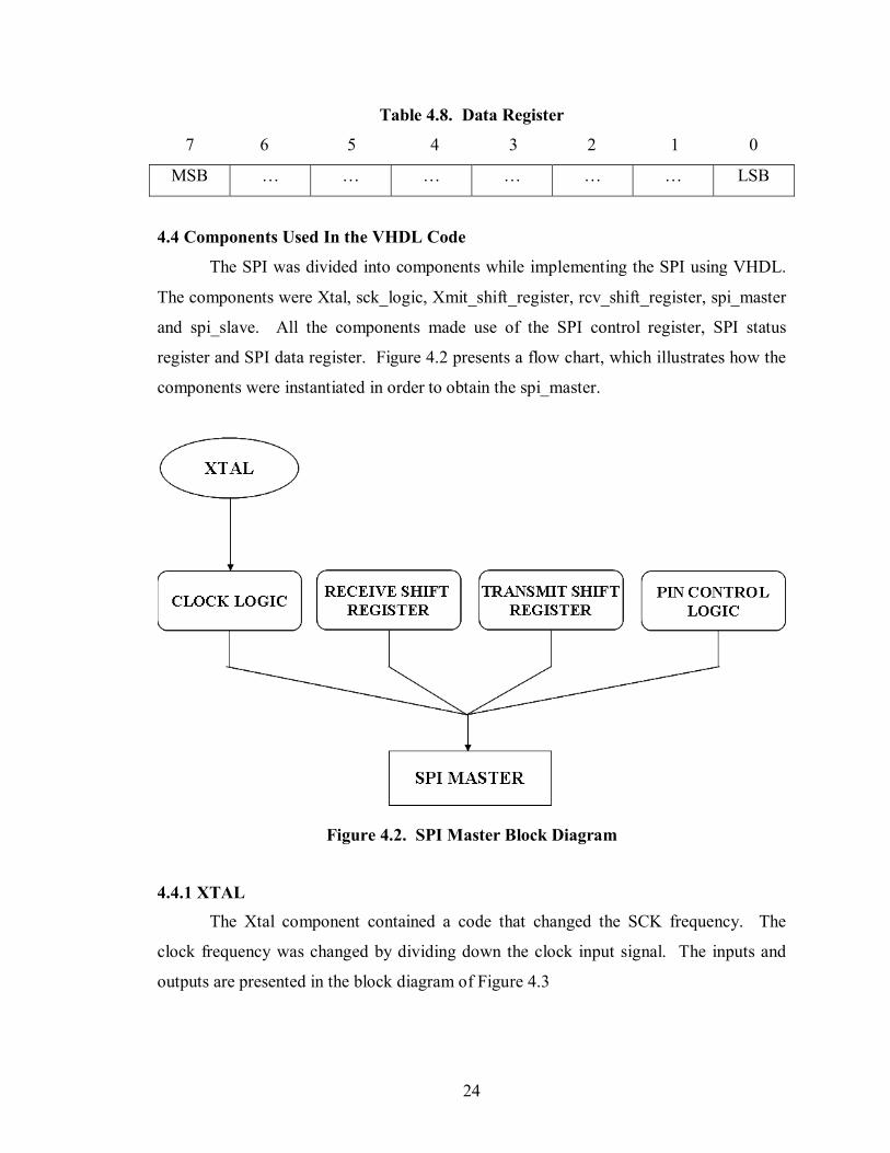
4.4 Components Used in the VHDL Code 24
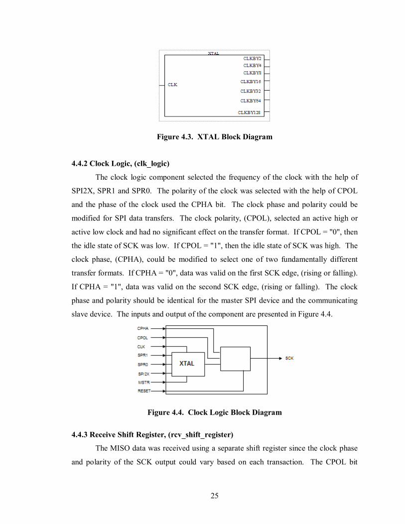
4.4.1 XTAL 24
4.4.2 Clock Logic, (clk_logic) 25
4.4.3 Receive Shift Register, (rcv_shift_register) 25
4.4.4 Transmit Shift Register, (xmit_shift_register) 26
4.4.5 Pin Control Logic, (pin_control_logic) 27
4.4.6 Serial Peripheral Interface, (SPI) 27
CHAPTER 5 INTRODUCTION TO QUARTUS II 28
CHAPTER 6 SIMULATION RESULTS 31
6.1 Xtal 31
6.2 Clock Logic 32
6.3 Receive Shift Register 33
6.4 Transmit Shift Register 34
6.5 Pin Control Logic 35
6.6 SPI Master 36
6.7 SPI Slave 37
CHAPTER 7 CONCLUSIONS AND RECOMMENDATIONS 38
REFERENCES 39
APPENDICES 41
iii
LIST OF TABLES
Table 1.1 7000S Device Features [7] 2
Table 1.2 JTAG Pin Descriptions for the CPLD [6] 3
Table 1.3 JTAG Pin Descriptions for the FPGA [8] 4
Table 3.1 Pin Configuration of MAX 7000 Devices [7] 14
Table 4.1 Direction of the Pins in Different Modes [12] 21
Table 4.2 SPI Control Register 21
Table 4.3 Master / Slave Bit Modes 22
Table 4.4 Clock Polarity Functionality [12] 22
Table 4.5 Clock Phase Functionality [12] 22
Table 4.6 Status Register 23
Table 4.7 Relation Between the Clock and Oscillator Frequency [12] 23
Table 4.8 Data Register 24
iv
LIST OF FIGURES
Figure 1.1 ISP-Capable CPLD Interface with ByteBlaster or MasterBlaster [6] 2
Figure 1.2 ISP-Capable CPLD Interface with ByteBlaster or MasterBlaster [8] 4
Figure 2.1 Connection Between the Host Controller and the Satellite Controllers [3] 5
Figure 2.2 SPI in a Sensor Bus [4] 7
Figure 2.3 Standard Architecture for the Servo Driver [5] 8
Figure 2.4 Data Transmission Between the Sensor and Servo Driver [5] 8
Figure 3.1 Schematic of the PCB Designed with a CPLD and JTAG 13
Figure 3.2 The Pin Diagram for the EPM 7128S 14
Figure 3.3 Top Layer of the PCB Design 15
Figure 3.4 Bottom Layer of the PCB Design 16
Figure 3.5 Top Overlay of the PCB Design 16
Figure 3.6 Multilayer View of the PCB Design 17
Figure 3.7 Keep-Out Layer of the PCB Design 17
Figure 3.8 Mechanical Layer of the PCB Design 18
Figure 3.9 Top View of the Populated Board 19
Figure 4.1 Block Diagram for a Serial Peripheral Interface [12] 20
Figure 4.2 SPI Master Block Diagram 24
Figure 4.3 XTAL Block Diagram 25
Figure 4.4 Clock Logic Block Diagram 25
Figure 4.5 Receive Shift Register Block Diagram 26
Figure 4.6 Transmit Shift Register Block Diagram 26
Figure 4.7 Pin Control Logic Block Diagram 27
Figure 4.8 Serial Peripheral Interface Block Diagram 27
Figure 6.1 Output of the XTAL when the MSRT Signal is ‘0’ 31
Figure 6.2 Output of the XTAL when the MSRT Signal is ‘1’ 32
Figure 6.3 Output of the Clock Logic when the MSRT Signal is ‘1’ 32

v
Figure 6.4 Output of the Clock Logic when the MSRT Signal is ‘0’ 33
Figure 6.5 Output of the Receive Shift Register when the CPOL Signal is ‘0’ 33
Figure 6.6 Output of the Receive Shift Register when the CPOL Signal is ‘0’ 34
Figure 6.7 Output of the Receive Shift Register when Shift_in is Enabled 34
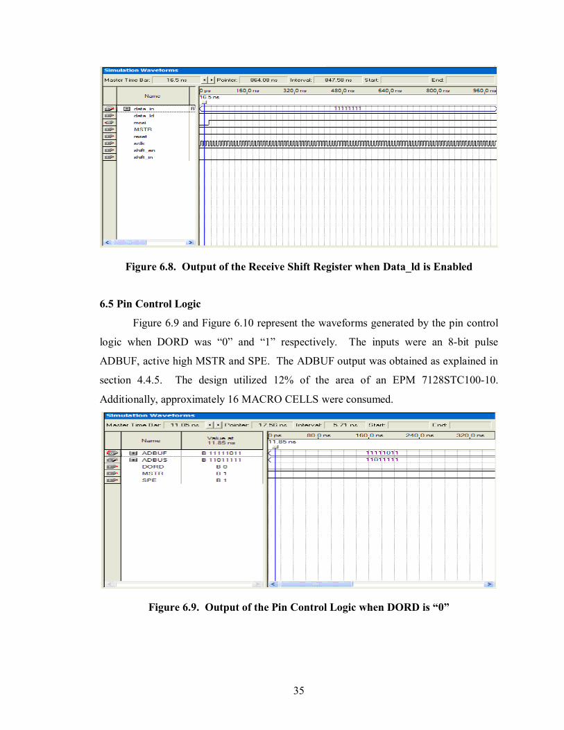
Figure 6.8 Output of the Receive Shift Register when Data_ld is Enabled 35
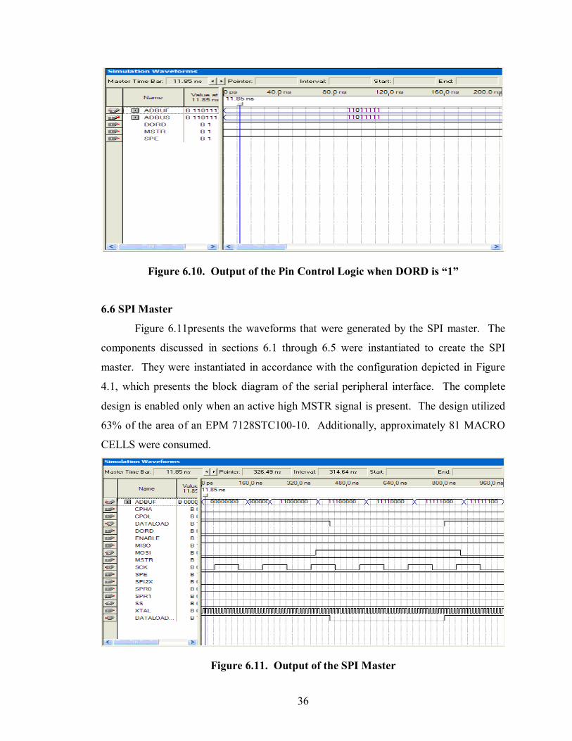
Figure 6.9 Output of the Pin Control Logic when DORD is “0” 35
Figure 6.10 Output of the Pin Control Logic when DORD is “1” 36
Figure 6.11 Output of the SPI Master 36
Figure 6.12 Output of the SPI Slave 37
vi
A DESIGN METHODOLOGY FOR IMPLEMENTATION OF SERIAL
PERIPHERAL INTERFACE USING VHDL
Jyothsna Kurapati
ABSTRACT
In this thesis, an approach is proposed for the design and implementation of a
serial peripheral interface using Complex Programmable Logic Devices, (CPLD's). The
focus of this research was to develop an effective Serial Peripheral Interface. The Serial
Peripheral Interface, (SPI), created by Motorola is also known as Microwire, which is a
trademark of National Semiconductor. The SPI is a full-duplex, synchronous, serial data
link that enables communication between a host processor and peripherals.
The Serial peripheral interface can be programmed in software or built strictly in
hardware inside a microcontroller. However, Complex programmable logic devices offer
a quicker and more customizable solution. This research investigated the Serial
peripheral interface with respect to its implementation in a CPLD and the use of the Very
High Speed Integrated Circuit Hardware Description language, (VHDL). Altera Quartus
II software was used for simulation and optimization of the synthesizable VHDL code.
Altera MAX 7000S Family devices were utilized for hardware evaluation. Design of a
printed circuit board using Protel Design Explorer was performed for this system.

1
CHAPTER 1
INTRODUCTON
FPGAs and CPLDs are being increasingly used in different applications because
of their low cost, re-programmability and capability for implementation of large designs
on a single chip. FPGAs such as the FLEX 10K devices are based on reconfigurable
CMOS SRAM elements with the Flexible Logic Element MatriX architecture, which
incorporates all the features necessary to implement common gate array megafunctions.
CPLDs such as the MAX 7000S are EEPROM-based programmable logic devices [1].
The name Serial Peripheral Interface, (SPI), which was created by Motorola, is
also known as Microwire and is a trademark of National Semiconductor. Both devices
possess the same functionality. The SPI is a full-duplex, synchronous serial data link that
enables communication between a host processor and peripherals [2].
The SPI is used in many applications such as:
i. Robot teleoperation, were the host controller and the satellite
controllers are networked via the SPI protocol, with a maximum speed
of 5Mbps [3].
ii. A sensor bus that is based on the serial peripheral interface [4].
iii. Communication between sensors and servo drivers [5].
In this research the SPI was implemented in a FPGA/CPLD using VHDL. VHDL
code can be downloaded onto an Altera FPGA/CPLD using a ByteBlaster or
MasterBlaster Cable. VHDL coding was performed with the aid of Quartus II software,
which was developed by Altera.
1.1 In-System Programmability
After the VHDL code was developed it was downloaded into the FPGA/CPLD.
The MAX 7000S and FLEX 10K devices are in-system programmable, (ISP), via an
industry-standard four-pin Joint Test Action Group, (JTAG), interface.
2
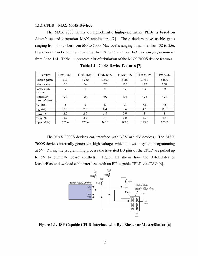
1.1.1 CPLD – MAX 7000S Devices
The MAX 7000 family of high-density, high-performance PLDs is based on
Altera’s second-generation MAX architecture [7]. These devices have usable gates
ranging from in number from 600 to 5000, Macrocells ranging in number from 32 to 256,
Logic array blocks ranging in number from 2 to 16 and User I/O pins ranging in number
from 36 to 164. Table 1.1 presents a brief tabulation of the MAX 7000S device features.
Table 1.1. 7000S Device Features [7]
The MAX 7000S devices can interface with 3.3V and 5V devices. The MAX
7000S devices internally generate a high voltage, which allows in-system programming
at 5V. During the programming process the tri-stated I/O pins of the CPLD are pulled up
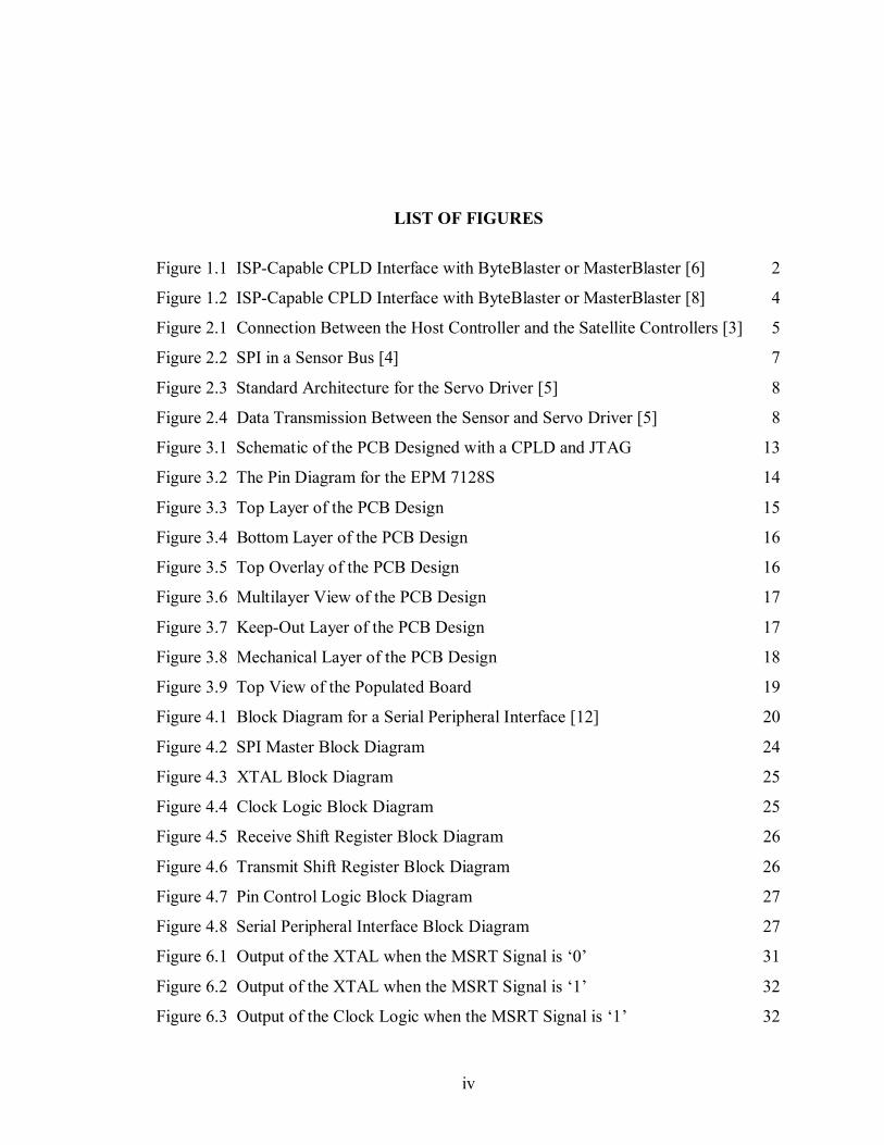
to 5V to eliminate board conflicts. Figure 1.1 shows how the ByteBlaster or
MasterBlaster download cable interfaces with an ISP-capable CPLD via JTAG [6].
Figure 1.1. ISP-Capable CPLD Interface with ByteBlaster or MasterBlaster [6]
3
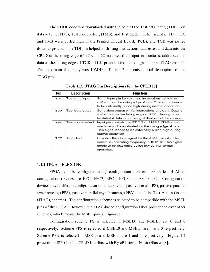
The VHDL code was downloaded with the help of the Test data input, (TDI), Test
data output, (TDO), Test mode select, (TMS), and Test clock, (TCK), signals. TDO, TDI
and TMS were pulled high in the Printed Circuit Board, (PCB), and TCK was pulled
down to ground. The TDI pin helped in shifting instructions, addresses and data into the
CPLD at the rising edge of TCK. TDO returned the output instructions, addresses and
data at the falling edge of TCK. TCK provided the clock signal for the JTAG circuits.
The maximum frequency was 10MHz. Table 1.2 presents a brief description of the
JTAG pins.
Table 1.2. JTAG Pin Descriptions for the CPLD [6]
1.1.2 FPGA – FLEX 10K
FPGAs can be configured using configuration devices. Examples of Altera
configuration devices are EPC, EPC2, EPC4, EPC8 and EPC16 [8]. Configuration
devices have different configuration schemes such as passive serial, (PS), passive parallel
synchronous, (PPS), passive parallel asynchronous, (PPA), and Joint Test Action Group,
(JTAG), schemes. The configuration scheme is selected to be compatible with the MSEL
pins of the FPGA. However, the JTAG-based configuration takes precedence over other
schemes, which means the MSEL pins are ignored.
Configuration scheme PS is selected if MSEL0 and MSEL1 are 0 and 0
respectively. Scheme PPS is selected if MSEL0 and MSEL1 are 1 and 0 respectively.
Scheme PPA is selected if MSEL0 and MSEL1 are 1 and 1 respectively. Figure 1.2
presents an ISP-Capable CPLD Interface with ByteBlaster or MasterBlaster [8].
4
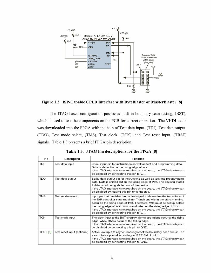
Figure 1.2. ISP-Capable CPLD Interface with ByteBlaster or MasterBlaster [8]
The JTAG based configuration possesses built in boundary scan testing, (BST),
which is used to test the components on the PCB for correct operation. The VHDL code
was downloaded into the FPGA with the help of Test data input, (TDI), Test data output,
(TDO), Test mode select, (TMS), Test clock, (TCK), and Test reset input, (TRST)
signals. Table 1.3 presents a brief FPGA pin description.
Table 1.3. JTAG Pin descriptions for the FPGA [8]

5
CHAPTER 2
APPLICATIONS FOR THE SERIAL PERIPHERAL INTERFACE
Different applications for the SPI are discussed briefly in this chapter.
2.1 Robotic Teleoperation
Robotic teleoperation is a concept of controlling robots using a master arm. A
distributed controller architecture for the master arm was developed to reduce non-
uniform time delays and to have higher position update capability. In the distributed
architecture the host controller and the satellite controllers are connected via the serial
peripheral interface, (SPI), protocol. The host controller acts as the master and the
satellite controllers are the slaves in the SPI protocol. Each joint has a satellite controller.
Satellite controllers are connected to the host controller in a daisy chained fashion
and the power line, clock, serial data out and serial data in lines are used for
communication. Figure 2.1 illustrates the connection between the host controller and the
satellite controllers.
Figure 2.1. Connection between Host Controller and Satellite Controllers [3]
Depending on the chip select signal, the host controller can communicate with
one satellite controller at a time. Selecting the satellite controller is accomplished
through the use of an identification number instead of chip select. Each satellite
controller has a unique identification number. The output, (SDO), of the satellite

6
controller is connected to the input, (SDI), of the host controller and vice versa. The
SDO signal is always disabled and the SDI signal is always enabled. The SDO signal of
the satellite controller is enabled when it receives its identification number. The satellite
controller performs the necessary operation and gets disabled.
The host controller, which is the master arm, is designed for measuring the
encoder values of the satellite controllers. The SPI protocol performs as follows:
i. The host controller enables the SDO of the satellite controller by sending
an identification number.
ii. The satellite controller associated with the identification number sends
two consecutive 8 bit encoder values to the host controller.
iii. The host controller receives the 16 bit encoder value from the
corresponding satellite controller.
iv. The SDO signal of the satellite controller is disabled.
v. Steps 1 to 4 are repeated.
The maximum communication speed is 5 MHz [3].
2.2 Sensor Bus
The sensor bus is used to transmit data from several digital smart sensors to an
internet interface. A master/slave type bus is used. The interface consists of an 8-byte
request from the master and a 32-byte response from the slave. The 32-byte output of the
slave is subdivided into an 8-byte header, which is used to identify the sensor and channel
number, followed by 24-bytes of sensor data.
The digital sensors can be connected to the internet through a PC with a web
connection and appropriate software. The SPI serial bus is widely available and is useful
for short runs and can be modified for long runs between the sensors. The master
supplies the clock signal. The exchange rate between the master and slave is 8-bytes for
8-clock cycles. Optical isolators are used to reduce the noise. A maximum of 9 remote
sensors can be connected to the local bus. Figure 2.2 illustrates the SPI in the sensor bus.

7
Figure2.2. SPI in a Sensor Bus [4]
The microprocessor connected to the network communication unit supplies the
clock for the circuit. The SPI in the sensor bus functions as follows:
i. Data transmitted from the master is sent to the SDI of the SPI bus in the
Microcontroller.
ii. Data from the slave remote sensor is sent to the SDO of the SPI bus in the
Microcontroller.
iii. The output isolator, which is the phototransistor, is pulled to 5V so that the
SDO line is 1 and does not allow the transfer of data.
iv. Steps 1 to 3 are repeated.
After sending the 8-byte request the master sends the required clock pulses for the
selected sensors to send their data, which consists of the 8-byte header and 24 bytes of
sensor data. The master stores the 32 bytes, formats it into an e-mail and transmits it
through the internet-compatible communication module [4].
8
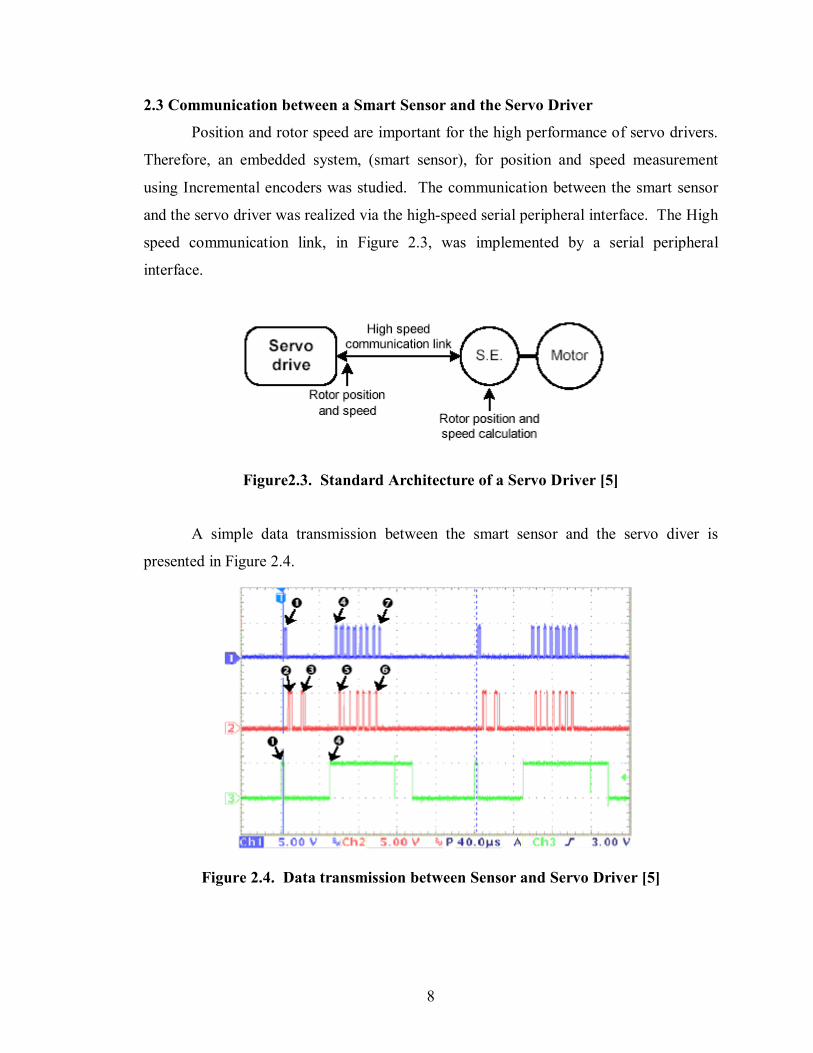
2.3 Communication between a Smart Sensor and the Servo Driver
Position and rotor speed are important for the high performance of servo drivers.
Therefore, an embedded system, (smart sensor), for position and speed measurement
using Incremental encoders was studied. The communication between the smart sensor
and the servo driver was realized via the high-speed serial peripheral interface. The High
speed communication link, in Figure 2.3, was implemented by a serial peripheral
interface.
Figure2.3. Standard Architecture of a Servo Driver [5]
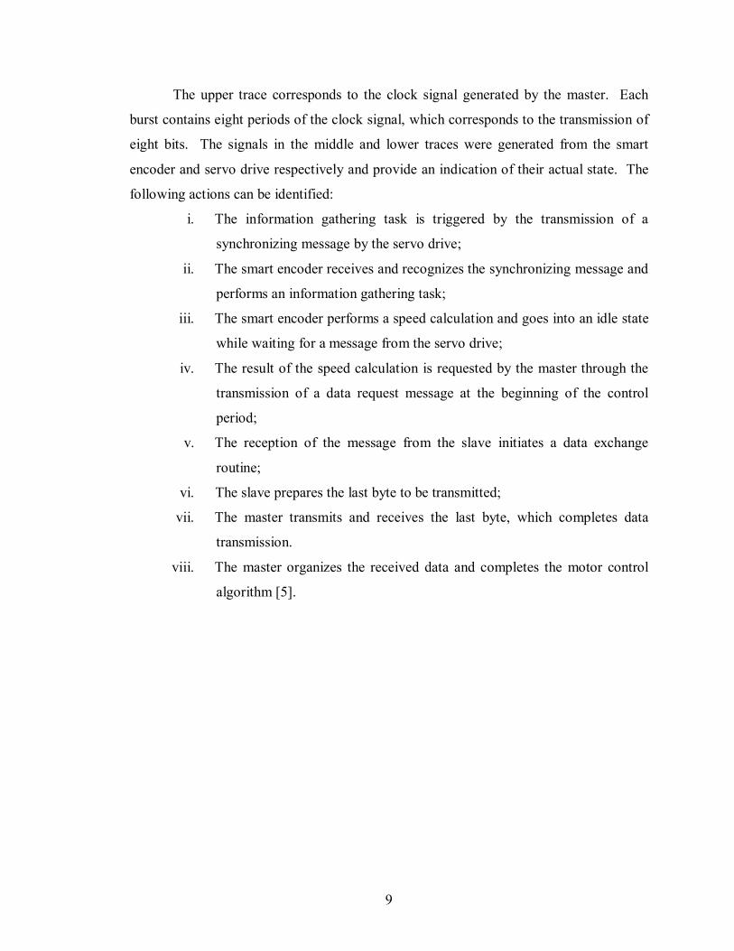
A simple data transmission between the smart sensor and the servo diver is
presented in Figure 2.4.
Figure 2.4. Data transmission between Sensor and Servo Driver [5]
9
The upper trace corresponds to the clock signal generated by the master. Each
burst contains eight periods of the clock signal, which corresponds to the transmission of
eight bits. The signals in the middle and lower traces were generated from the smart
encoder and servo drive respectively and provide an indication of their actual state. The
following actions can be identified:
i. The information gathering task is triggered by the transmission of a
synchronizing message by the servo drive;
ii. The smart encoder receives and recognizes the synchronizing message and
performs an information gathering task;
iii. The smart encoder performs a speed calculation and goes into an idle state
while waiting for a message from the servo drive;
iv. The result of the speed calculation is requested by the master through the
transmission of a data request message at the beginning of the control
period;
v. The reception of the message from the slave initiates a data exchange
routine;
vi. The slave prepares the last byte to be transmitted;
vii. The master transmits and receives the last byte, which completes data
transmission.
viii. The master organizes the received data and completes the motor control
algorithm [5].
10
CHAPTER 3
INTRODUCTION TO PCB DESIGN USING PROTEL
The VHDL code for the circuit was compiled and simulated using the Altera
Quartus II software. The next step created a prototype for the circuit using PCB design.
Once the PCB for the circuit was available, the input signals from the field to this board
were applied in order to check for the desired output. The PCB design was carried out
using PROTEL Design Explorer software. Protel DXP provides a versatile and fully
integrated design capture system for both PCB and FPGA applications. A design can be
captured using schematic capture only or any mixture of schematic capture and VHDL
for an FPGA design. Protel is a complete 32-bit electronic design system for Windows
2000 and XP. Protel provides a complete design suit that allows a design to be advanced
from the concept stage to the final board design. This research produced a designed for a
PCB with a CPLD and JTAG interface. The steps involved included board design,
schematic capture and PCB layout and routing.
Given, the increasing complexity and time associated with today’s electronic
projects, the requirement to negotiate a maze of loosely connected point tools, in order to
complete a design, must be avoided. Protel provides a multi-layer design environment
that includes:
i. True hierarchical, multi-channel schematic capture,
ii. Mixed mode SPICE 3f5 /XSpice simulation,
iii. Pre and post-layout signal integrity analysis,
iv. Rules driven board layout and editing,
v. Situs topological auto-routing,
vi. Complete CAM output and editing capabilities,
vii. Full support for schematic and VHDL-based FPGA design,
viii. Automatic pin synchronization between PCB and FPGA design projects,
11
ix. A reconfigurable development platform, which is the nano-board for
interactive implementation and debugging of FPGA based designs.
3.1 Rules Driven Layout and Routing
With Protel’s rules driving the PCB layout and editing environment, the designer
maintains full control over the board design process through the use of an extensive setup
of fully configurable design rules. Protel enforces relevant rules throughout the process,
which minimizes the probability of design errors. Protel 2004 brings a higher level of
control to interactive routing with a number of powerful routing modes to suit any routing
challenge.
3.2 Situs Topological Autorouting
With the inclusion of Altium’s new Situs Topological Autorouting System, Protel
provides the power to cope with high-density component packaging and tightly-packed
board designs. Unlike traditional shape-based routers, Protel’s topological autorouter has
the ability to natively find routing paths in non-orthogonal directions, which allows the
intelligent assignment of connections to layers. Topological path mapping also allows
Protel to efficiently route boards and components of any geometry without the need for
extensive post-route cleanup. In Protel 2004, Situs has been enhanced to provide
superior completion rates, better support for plane layers and split planes and support for
neck down pad entries.
3.3 Integrated Mixed Signal Simulation
Protel 2004 makes integrated signal and system integrity a reality. Protel 2004
allows the designer to run mixed signals spice, 3f5 X-Spice simulations directly from the
schematic editor and have the full complement of advanced simulation analysis available.
3.4 Pre and Post-Layout Signal Integrity Analysis
This capability allows the designer to dentify potential signal integrity problems
before board layout by running Protel’s signal integrity simulator on the design

12
schematic. Therefore, the designer can check the final PCB, after routing, to insure the
integrity of all signal paths in the design.
3.5 Integration of the PCB and FPGA Designs
Based on altiums new live design enabled DXP platform, Protel 2004 is the only
design system that allows the designer to effectively create and implement an FPGA
design and then carry the design all the way to the final PCB. To facilitate the design of
FPGAs, Protel 2004 comes with altiums unique Nano Board, which is a reconfigurable
development platform that acts like a nano level board and allows the designer to
download a design to an FPGA at any time in the design process. A combination of
virtual instruments and BST enable interactive debugging of the FPGA design. The
tedious and error prone task of synchronizing FPGA pin assignments between the PCB
and FPGA projects is handled automatically by the system and a range of FPGA pin
swapping features allows the designer to automatically optimize FPGA based board
design for routing.
3.6 Complete and Configurable Board-Level Design Environment
The combination of advanced design capabilities and superior ease of use make
Protel the most sophisticated and productive of the available electronics design tools.
Protel 2004 delivers a configurable design system that supports both the work flow and
the work environment. Protel 2004 is a design system that works with the natural design
process and not against it. Protel 2004 is a design system with all core features integrated
into a package at an affordable price that supports the use of high capacity programmable
devices.
3.7 Schematic Document of the Circuit
Protel DXP provides a versatile and fully integrated design capture system for
both PCB and FPGA applications. Designs can be captured using schematic capture or
any mixture of schematic capture and VHDL for an FPGA design. The schematic editor
supports both top-down and bottom-up design through the use of a block diagram
metaphor to provide an intuitive link between the sheets in the project hierarchy where
13
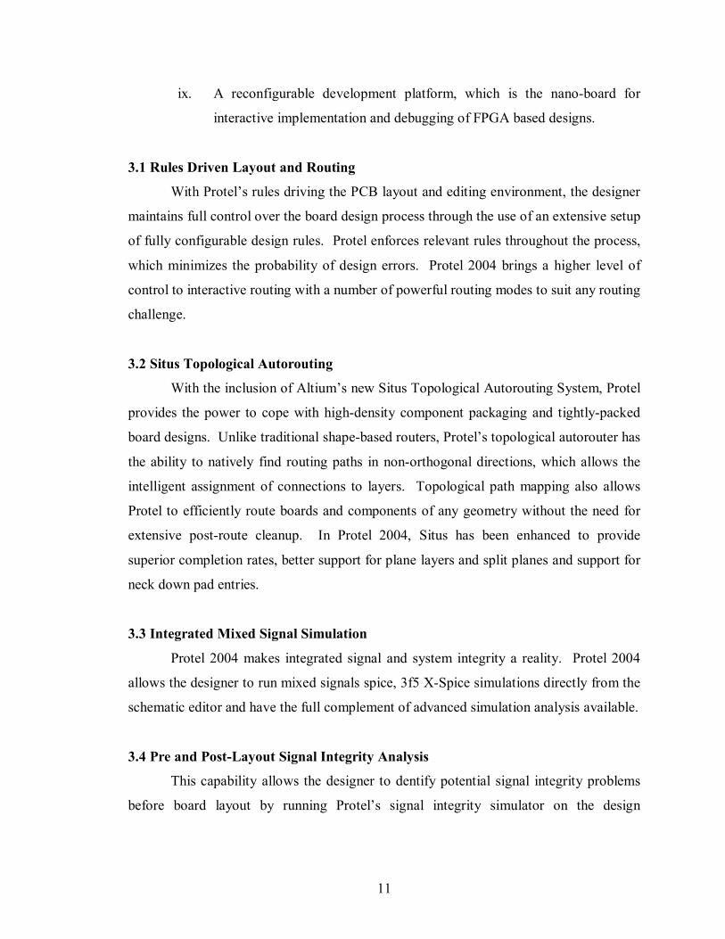
each block represents an individual schematic sheet. Wiring the blocks together creates
connectivity that can be verified and navigated as soon as the design is compiled. Figure
3.1 presents the schematic of the PCB designed with a CPLD and JTAG.
Figure 3.1. Schematic of the PCB Designed with a CPLD and JTAG
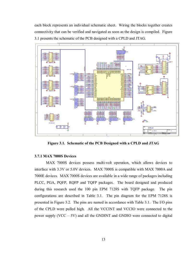
3.7.1 MAX 7000S Devices
MAX 7000S devices possess multi-volt operation, which allows devices to
interface with 3.3V or 5.0V devices. MAX 7000S is compatible with MAX 7000A and
7000E devices. MAX 7000S devices are available in a wide range of packages including
PLCC, PGA, PQFP, RQFP and TQFP packages. The board designed and produced
during this research used the 100 pin EPM 7128S with TQFP package. The pin
configurations are described in Table 3.1. The pin diagram for the EPM 7128S is
presented in Figure 3.2. The pins are named in accordance with Table 3.1. The I/O pins
of the CPLD were pulled high. All the VCCINT and VCCIO were connected to the
power supply (VCC – 5V) and all the GNDINT and GNDIO were connected to digital
14
ground, (DGND), in the PCB. TDI, TMS, TDO and TCK were connected to the JTAG
interface of the board as per the in-system programmability rules presented in Chapter 1.
Table3.1. Pin Configuration of MAX 7000 Devices [7]
Figure 3.2. The pin diagram for the EPM 7128S
15
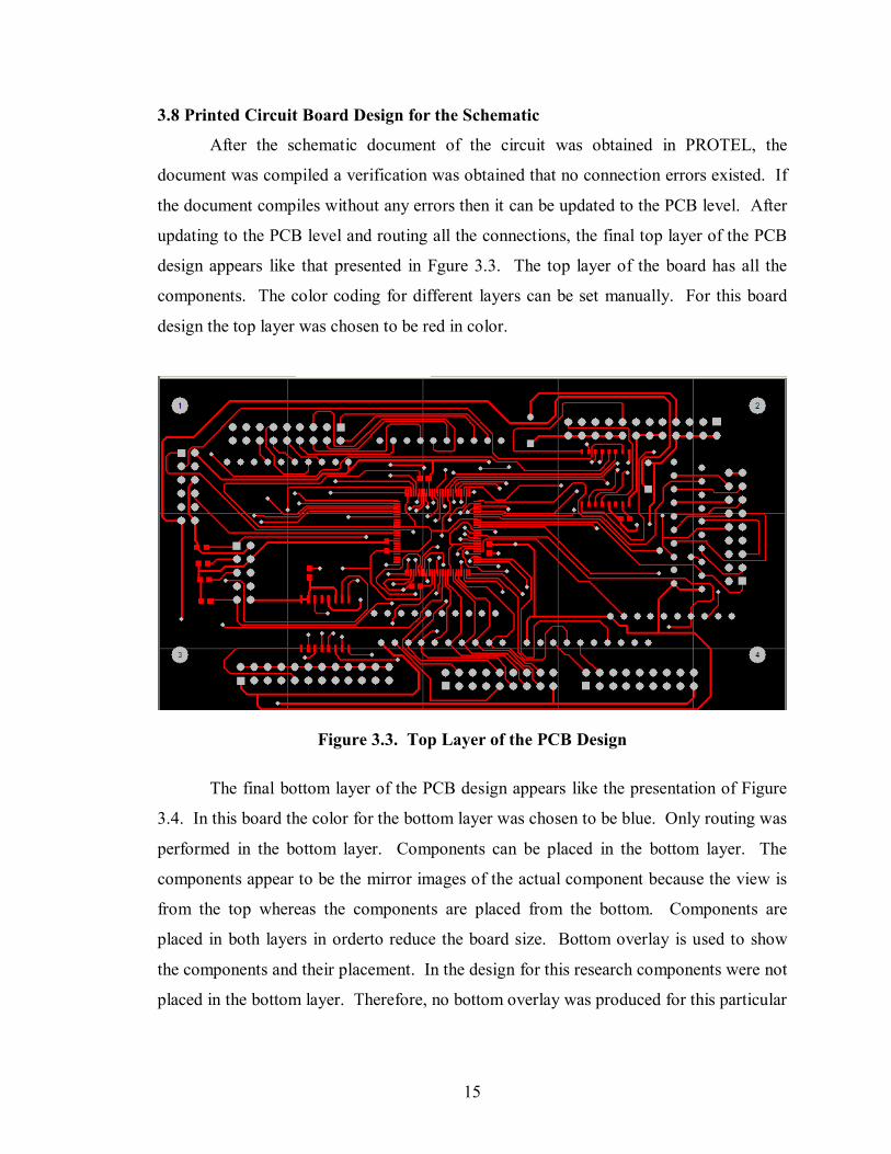
3.8 Printed Circuit Board Design for the Schematic
After the schematic document of the circuit was obtained in PROTEL, the
document was compiled a verification was obtained that no connection errors existed. If
the document compiles without any errors then it can be updated to the PCB level. After
updating to the PCB level and routing all the connections, the final top layer of the PCB
design appears like that presented in Fgure 3.3. The top layer of the board has all the
components. The color coding for different layers can be set manually. For this board
design the top layer was chosen to be red in color.
Figure 3.3. Top Layer of the PCB Design
The final bottom layer of the PCB design appears like the presentation of Figure
3.4. In this board the color for the bottom layer was chosen to be blue. Only routing was
performed in the bottom layer. Components can be placed in the bottom layer. The
components appear to be the mirror images of the actual component because the view is
from the top whereas the components are placed from the bottom. Components are
placed in both layers in orderto reduce the board size. Bottom overlay is used to show
the components and their placement. In the design for this research components were not
placed in the bottom layer. Therefore, no bottom overlay was produced for this particular
16
board. Component naming also appears as a mirror image in the bottom overlay of any
board.
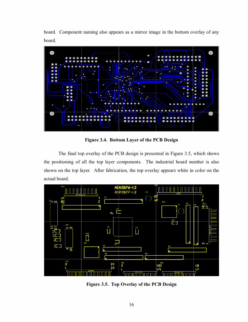
Figure 3.4. Bottom Layer of the PCB Design
The final top overlay of the PCB design is presented in Figure 3.5, which shows
the positioning of all the top layer components. The industrial board number is also
shown on the top layer. After fabrication, the top overlay appears white in color on the
actual board.
Figure 3.5. Top Overlay of the PCB Design
17
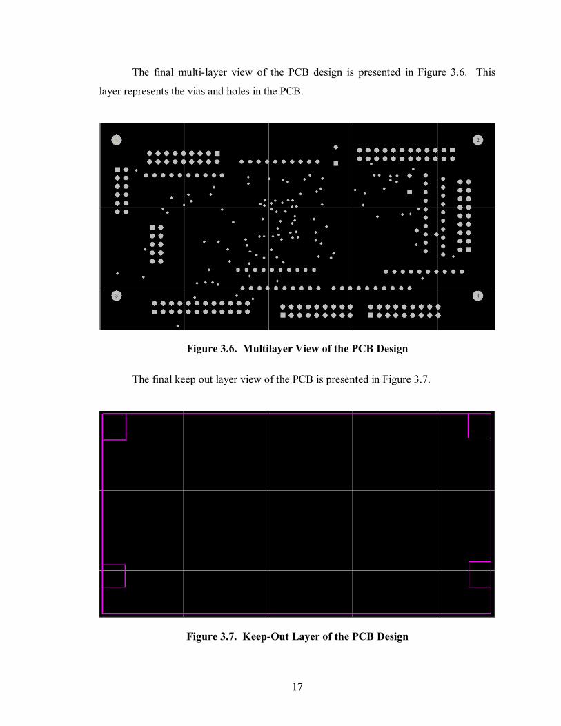
The final multi-layer view of the PCB design is presented in Figure 3.6. This
layer represents the vias and holes in the PCB.
Figure 3.6. Multilayer View of the PCB Design
The final keep out layer view of the PCB is presented in Figure 3.7.
Figure 3.7. Keep-Out Layer of the PCB Design
18
The keep-out layer was used in the area of high voltage or high impedance to
prevent the auto-router from running a trace through that area. The color code for the
keep-out layer was pink for this board.
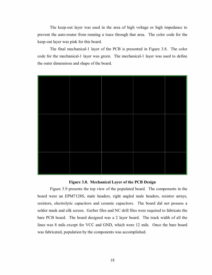
The final mechanical-1 layer of the PCB is presented in Figure 3.8. The color
code for the mechanical-1 layer was green. The mechanical-1 layer was used to define
the outer dimensions and shape of the board.
Figure 3.8. Mechanical Layer of the PCB Design Figure 3.9 presents the top view of the populated board. The components in the
board were an EPM7128S, male headers, right angled male headers, resistor arrays,
resistors, electrolytic capacitors and ceramic capacitors. The board did not possess a
solder mask and silk screen. Gerber files and NC drill files were required to fabricate the
bare PCB board. The board designed was a 2 layer board. The track width of all the
lines was 8 mils except for VCC and GND, which were 12 mils. Once the bare board
was fabricated, population by the components was accomplished.

19
Figure 3.9. Top View of the Populated Board

20
CHAPTER 4
SERIAL PERIPHERAL INTERFACE USING VHDL
The ATMEGA 128 Microcontroller’s SPI along with the components used for
writing the VHDL code is discussed in this chapter. The block diagram of the interface is
presented in Figure 4.1.
Figure 4.1. Block Diagram of the Serial Peripheral Interface [12] As discussed earlier, the SPI possessed two modes, which were the master mode
and the slave mode. The data direction of the MOSI, (Master Out Slave In), MISO,
(Master In Slave Out), SCK, (System Clock), and SS, (Slave Select) pins are presented in
Table 4.1. The clock, (SCK), signal was generated by the CPLD when it was in the
master mode. During the slave mode, the clock was an input from the peripheral device.
In master mode the MOSI, SCK and SS pins were user defined, whereas the MISO was
21
the input to the CPLD. The SS bit was used to change the master mode to the slave
mode. When SS = ‘0’ the CPLD was in the slave mode and when SS = ‘1’ the CPLD
was in the master mode.
Table 4. 1. Direction of the Pins in Different Modes [12]
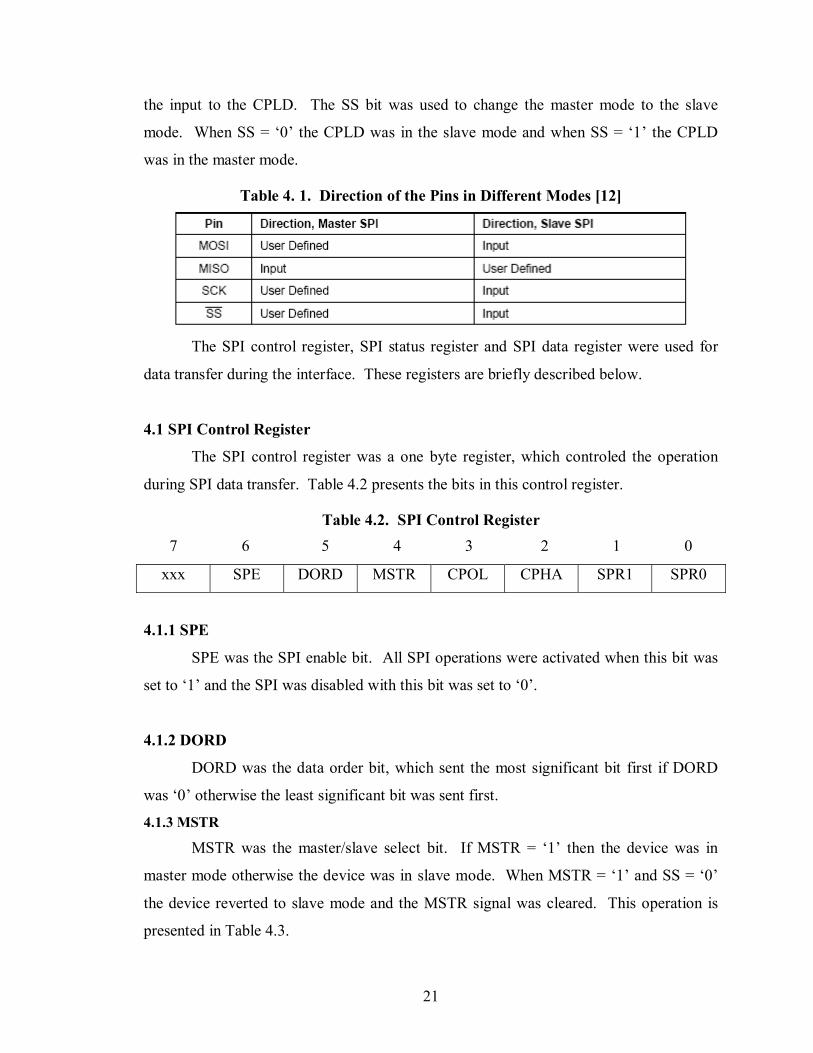
The SPI control register, SPI status register and SPI data register were used for
data transfer during the interface. These registers are briefly described below.
4.1 SPI Control Register
The SPI control register was a one byte register, which controled the operation
during SPI data transfer. Table 4.2 presents the bits in this control register.
Table 4.2. SPI Control Register 7 6 5 4 3 2 1 0
xxx SPE DORD MSTR CPOL CPHA SPR1 SPR0
4.1.1 SPE
SPE was the SPI enable bit. All SPI operations were activated when this bit was
set to ‘1’ and the SPI was disabled with this bit was set to ‘0’.
4.1.2 DORD
DORD was the data order bit, which sent the most significant bit first if DORD
was ‘0’ otherwise the least significant bit was sent first.
4.1.3 MSTR
MSTR was the master/slave select bit. If MSTR = ‘1’ then the device was in
master mode otherwise the device was in slave mode. When MSTR = ‘1’ and SS = ‘0’
the device reverted to slave mode and the MSTR signal was cleared. This operation is
presented in Table 4.3.

22
Table 4.3. Master/Slave Bit Modes
1. MSTR 2. MODE
3. 1 4. Master
5. 0 6. Slave
4.1.4 CPOL
CPOL was a clock polarity bit and its operation is presented in Table 4.4.
Table 4.4. Clock Polarity Functionality [12]
If CPOL= ‘1’ the leading edge of SCK is treated as the falling edge and when CPOL
=‘0’, the leading edge of the SCK is treated as the rising edge.
4.1.5 CPHA
CPHA was a clock phase bit and its operation is described in Table 4.5. If CPHA = ‘0’
the data was sampled during the leading edge. However, the data was sampled during the
trailing edge when CPHA = ‘1’.
Table 4.5. Clock phase Functionality [12]
4.1.6 SPR1
The SPR1 signal controled the SCK, (system clock), rate of the device.
4.1.7 SPR0
The SPRO signal also controled the SCK rate of the device.
23
4.2 SPI Status Register
The SPI status register was a 1 byte register. The bits in this register are
presented in Table 4.6. Bits 5 to 1 are reserved bits in the ATMEGA 128
microcontroller.
Table 4.6 Status Register 7 6 5 4 3 2 1 0
XXX XXX - - - - - SPI2X
4.2.1 SPI2X
The SPI2X controlled the SCK rate of the device. The relation between SPR1,
SPR0, SPI2X, SCK and the oscillator frequency, (fosc), is presented in Table 4.7
Table 4.7. Relation between the Clock and Oscillator Frequency [12]
4.3 SPI Data Register
The SPI data register was an 8 bit read/write register used to store data during
data transfer. If data was written to this register it acted as a buffer and if data was sent
from this register it acted as a shift register. Writing data was performed during the
master operation and reading was performed during the slave operation. The bits are
presented in Table 4.8 [11].
24
Table 4.8. Data Register
7 6 5 4 3 2 1 0
MSB … … … … … … LSB
4.4 Components Used In the VHDL Code
The SPI was divided into components while implementing the SPI using VHDL.
The components were Xtal, sck_logic, Xmit_shift_register, rcv_shift_register, spi_master
and spi_slave. All the components made use of the SPI control register, SPI status
register and SPI data register. Figure 4.2 presents a flow chart, which illustrates how the
components were instantiated in order to obtain the spi_master.
Figure 4.2. SPI Master Block Diagram
4.4.1 XTAL The Xtal component contained a code that changed the SCK frequency. The
clock frequency was changed by dividing down the clock input signal. The inputs and
outputs are presented in the block diagram of Figure 4.3
25
Figure 4.3. XTAL Block Diagram
4.4.2 Clock Logic, (clk_logic)
The clock logic component selected the frequency of the clock with the help of
SPI2X, SPR1 and SPR0. The polarity of the clock was selected with the help of CPOL
and the phase of the clock used the CPHA bit. The clock phase and polarity could be
modified for SPI data transfers. The clock polarity, (CPOL), selected an active high or
active low clock and had no significant effect on the transfer format. If CPOL = "0", then
the idle state of SCK was low. If CPOL = "1", then the idle state of SCK was high. The
clock phase, (CPHA), could be modified to select one of two fundamentally different
transfer formats. If CPHA = "0", data was valid on the first SCK edge, (rising or falling).
If CPHA = "1", data was valid on the second SCK edge, (rising or falling). The clock
phase and polarity should be identical for the master SPI device and the communicating
slave device. The inputs and output of the component are presented in Figure 4.4.
Figure 4.4. Clock Logic Block Diagram
4.4.3 Receive Shift Register, (rcv_shift_register)
The MISO data was received using a separate shift register since the clock phase
and polarity of the SCK output could vary based on each transaction. The CPOL bit

26
specified if the external SCK incoming MISO data was sampled on. This accounted for
the fact that some of the SPI slave devices were SPI slaves with clock data out on the
rising edge of SCK while others provided clock data out on the falling edge of SCK. If a
slave clocked data out on the falling edge of SCK, then the clock polarity was set to "1"
so that the SPI Master would clock data in on the rising edge of SCK. If a slave clocked
data out on the rising edge of SCK, then CPOL was set to "0" so that the SPI Master
clocked data in on the falling edge of SCK. The inputs and output of the component are
presented in Figure 4.5.
Figure 4.5. Receive Shift Register Block Diagram
4.4.4 Transmit Shift Register, (xmit_shift_register)
The transmit shift register controlled the shift and load operations of the SPI. It
also monitored the SPI bus and determined when a byte transfer was complete. The SPI
transmit shift register was an 8-bit loadable shift register. This shift register was loaded
from the SPI Transmit Register, (SPITR), via a load signal generated by the SPI control
state machine and was clocked by the rising edge of SCK. The MOSI data was shifted
out. The load signal used in the code was Data_ld. The data was shifted into the register
with the shift enable signal. The inputs and output of the component are presented in
Figure 4.6
Figure 4.6. Transmit Shift Register Block Diagram

27
4.4.5 Pin Control Logic, (pin_control_logic) The data order bit specified the input and output control logic in the serial
peripheral interface. The output bits were reversed if DORD was “0”, whereas they were
transmitted directly if DORD was”1” The inputs and output of the component are
presented in Figure 4.7
Figure 4.7. Pin Control Logic Block Diagram
4.4.6 Serial Peripheral Interface, (SPI)
Spi_master and spi_slave were combined to produce the SPI. Figure 4.8 presents
the components used to build the interface.
Figure 4.8. Serial Peripheral Interface Block Diagram

28
CHAPTER 5
INTRODUCTION TO QUARTUS II TOOL
Altera’s Quartus II is a PLD Design Software system, which is suitable for high-
density Field-Programmable Gate Array, (FPGA), designs, low-cost FPGA designs and
Complex Programmable Logic Device, (CPLD), designs. The possible file types used in
Quartus include schematics, Verilog code and other hardware description language files
such as VHDL and AHDL, which is Altera’s proprietary HDL. It is also possible to use a
third-party synthesis tool to generate a file that represents the circuit in a standard format
called EDIF, (Electronic Design Interface Format).
The Quartus II software includes a modular Compiler. The Compiler includes the
following modules; modules marked with an asterisk are optional during a full
compilation and depend on selected settings:
i. Analysis & Synthesis
ii. Partition Merge*
iii. Fitter
iv. Assembler*
v. Timing Analyzer*
vi. Design Assistant*
vii. EDA Netlist Writer*
viii. HardCopy Netlist Writer*
The following steps describe the basic design flow for the Quartus II graphical user
interface:
i. Create a new project and specify a target device or device family by using
the New Project Wizard, (File menu).

29
ii. Create a Verilog HDL, VHDL or Altera Hardware Description Language,
(AHDL), design by using the Text Editor. The Block Editor can be used
to create a block diagram with symbols that represent other design files or
to create a schematic. The MegaWizard Plug-In Manager, (Tools menu),
can be used to generate custom variations of megafunctions and IP
functions to be instantiated in a design.
iii. (Optional), Specify initial design constraints using the Assignment Editor,
the Pin Planner and the Settings dialog box, (Assignments menu), the
Floorplan Editor, the Design Partitions window and/or the LogicLock™
feature.
iv. (Optional), Perform an Early Timing Estimate to generate early estimates
of timing results before the Fitter is complete.
v. (Optional), Create a system-level design using the SOPC Builder or DSP
Builder.
vi. (Optional), Create software and programming files for Excalibur device
processors or Nios II embedded processors using the Software Builder.
vii. Synthesize the design using Analysis & Synthesis.
viii. (Optional), If a design contains partitions and a full compilation is not
being performed, merge the partitions with Partition Merge.
ix. (Optional), Perform functional simulation by using the Simulator and the
Generate Functional Simulation Netlist command.
x. Perform place and route by using the Fitter.
xi. Perform a power estimation and analysis using the PowerPlay Power
Analyzer.
xii. Perform timing analysis using the Timing Analyzer.
xiii. Perform timing simulation using the Simulator.
xiv. (Optional), Make timing improvements, to achieve timing closure, using
physical synthesis, the Timing Closure floorplan, the LogicLock feature,
the Settings dialog box and the Assignment Editor.
xv. Create programming files using the Assembler.
30
xvi. Program the device using programming files, the Programmer and Altera
hardware or convert programming files to other file formats for use by
other systems such as embedded processors.
xvii. (Optional), Debug a design using the SignalTap II Logic Analyzer, the
SignalProbe feature or the Chip Editor.
xviii. (Optional), Manage engineering changes using the Chip Editor, the
Resource Property Editor and the Change Manager [10].
Altera offers programmable logic devices, (PLD), such as APEX 20K, ACEX 1K,
APEX II, Excalibur, Cyclone, Cyclone II, FLEX 6000, FLEX 10K, HardCopy II,
HardCopy Stratix, MAX II, MAX 3000, MAX 7000, Mercury, Stratix, Stratix II and
Stratix GX device families. Quartus allows users, familiar with other PLD tools, to
integrate designs in those tools with Quartus II generated projects.
Altera also offers serial configuration devices, such as EPC1, EPC1441, EPC2,
EPC4, EPC8, EPC16 and EPCS64, which are used to configure the ACEX 1K, APEX
20K, APEX II, Excalibur, Cyclone, Cyclone II, FLEX 6000, FLEX 10K, Mercury,
Stratix, Stratix II and Stratix GX device families.
Quartus has a system-on-a-programmable-chip, (SOPC), builder. SOPC Builder
is a powerful system development tool for creating systems based on processors,
peripherals and memories. SOPC Builder enables the designer to define and generate a
complete SOPC in much less time than would be required when using traditional,
manual, integration methods.
The software used to in this research was Altera Quartus II, version 5.0, which
supports all MAX® II, Cyclone™ II and Cyclone devices. Altera Quartus II, version 5.0
supports selected Stratix® II, Stratix, APEX™ 20KE, ACEX®, FLEX® 10KE, FLEX
10K®, FLEX 10KA, FLEX 6000, MAX 7000S, MAX 7000B, MAX 7000AE, and MAX
3000A devices [1].
31
CHAPTER 6
SIMULATION RESULTS
Simulation results of all the individual components, which were used to build the
interface using VHDL, are discussed in this chapter.
6.1 Xtal
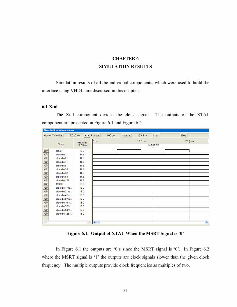
The Xtal component divides the clock signal. The outputs of the XTAL
component are presented in Figure 6.1 and Figure 6.2.
Figure 6.1. Output of XTAL When the MSRT Signal is ‘0’
In Figure 6.1 the outputs are ‘0’s since the MSRT signal is ‘0’. In Figure 6.2
where the MSRT signal is ‘1’ the outputs are clock signals slower than the given clock
frequency. The multiple outputs provide clock frequencies as multiples of two.
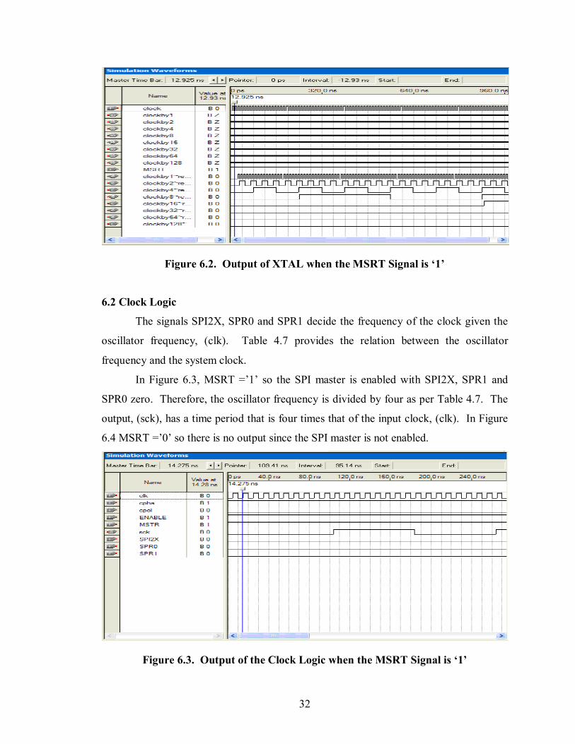
32
Figure 6.2. Output of XTAL when the MSRT Signal is ‘1’
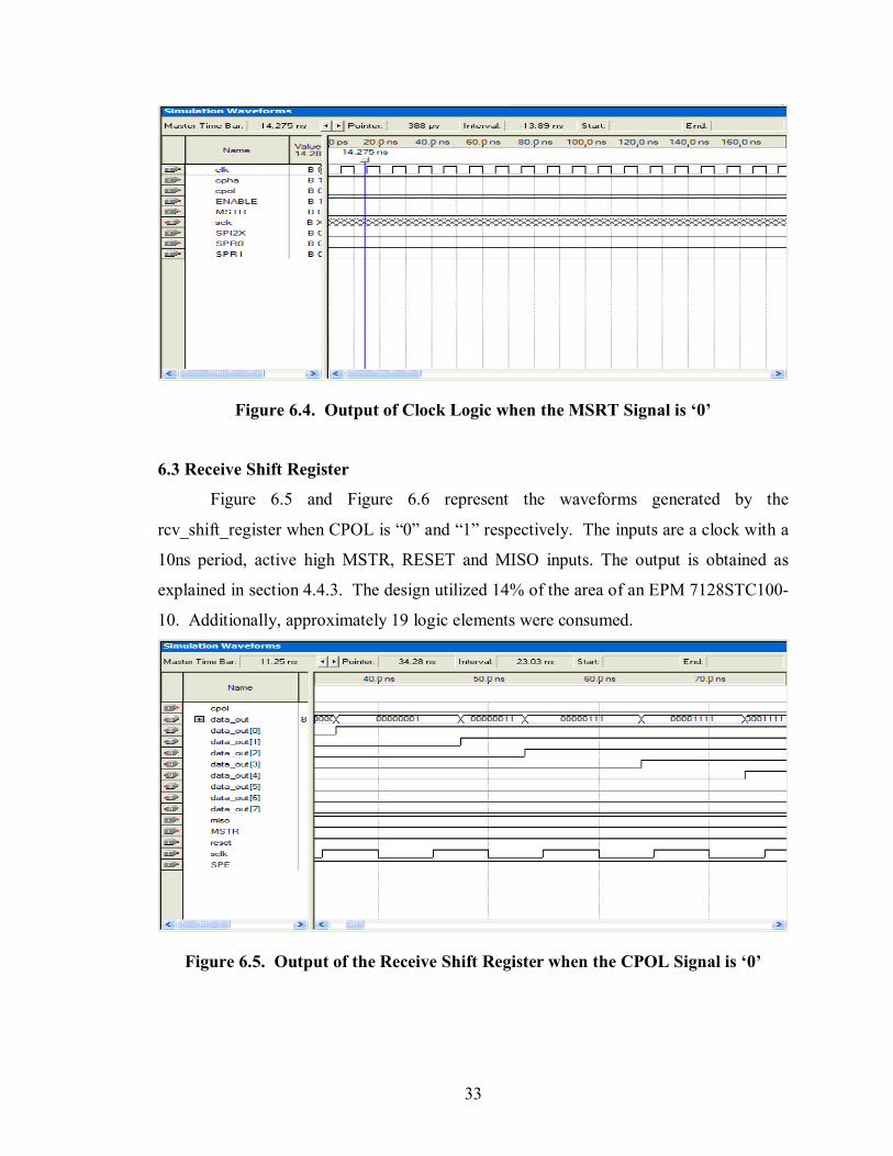
6.2 Clock Logic
The signals SPI2X, SPR0 and SPR1 decide the frequency of the clock given the
oscillator frequency, (clk). Table 4.7 provides the relation between the oscillator
frequency and the system clock.
In Figure 6.3, MSRT =’1’ so the SPI master is enabled with SPI2X, SPR1 and
SPR0 zero. Therefore, the oscillator frequency is divided by four as per Table 4.7. The
output, (sck), has a time period that is four times that of the input clock, (clk). In Figure
6.4 MSRT =’0’ so there is no output since the SPI master is not enabled.
Figure 6.3. Output of the Clock Logic when the MSRT Signal is ‘1’
33
Figure 6.4. Output of Clock Logic when the MSRT Signal is ‘0’
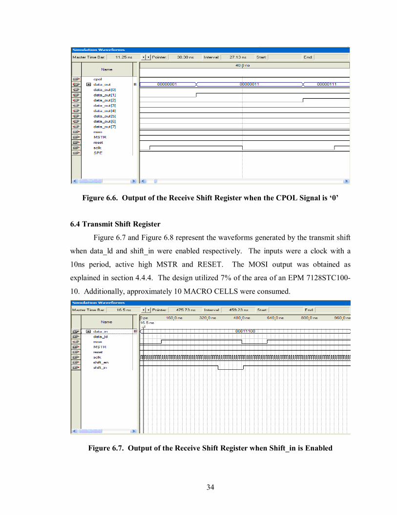
6.3 Receive Shift Register
Figure 6.5 and Figure 6.6 represent the waveforms generated by the
rcv_shift_register when CPOL is “0” and “1” respectively. The inputs are a clock with a
10ns period, active high MSTR, RESET and MISO inputs. The output is obtained as
explained in section 4.4.3. The design utilized 14% of the area of an EPM 7128STC100-
10. Additionally, approximately 19 logic elements were consumed.
Figure 6.5. Output of the Receive Shift Register when the CPOL Signal is ‘0’
34
Figure 6.6. Output of the Receive Shift Register when the CPOL Signal is ‘0’
6.4 Transmit Shift Register
Figure 6.7 and Figure 6.8 represent the waveforms generated by the transmit shift
when data_ld and shift_in were enabled respectively. The inputs were a clock with a
10ns period, active high MSTR and RESET. The MOSI output was obtained as
explained in section 4.4.4. The design utilized 7% of the area of an EPM 7128STC100-
10. Additionally, approximately 10 MACRO CELLS were consumed.
Figure 6.7. Output of the Receive Shift Register when Shift_in is Enabled
35
Figure 6.8. Output of the Receive Shift Register when Data_ld is Enabled
6.5 Pin Control Logic
Figure 6.9 and Figure 6.10 represent the waveforms generated by the pin control
logic when DORD was “0” and “1” respectively. The inputs were an 8-bit pulse
ADBUF, active high MSTR and SPE. The ADBUF output was obtained as explained in
section 4.4.5. The design utilized 12% of the area of an EPM 7128STC100-10.
Additionally, approximately 16 MACRO CELLS were consumed.
Figure 6.9. Output of the Pin Control Logic when DORD is “0”
36
Figure 6.10. Output of the Pin Control Logic when DORD is “1”
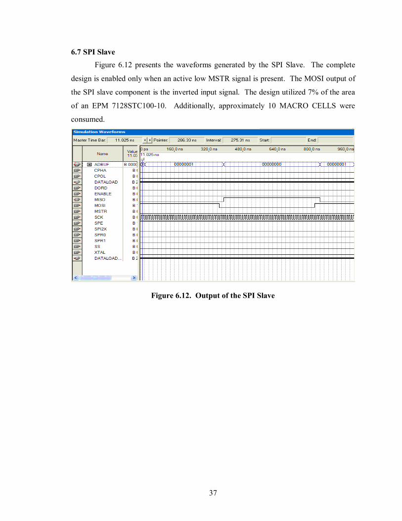
6.6 SPI Master
Figure 6.11presents the waveforms that were generated by the SPI master. The
components discussed in sections 6.1 through 6.5 were instantiated to create the SPI
master. They were instantiated in accordance with the configuration depicted in Figure
4.1, which presents the block diagram of the serial peripheral interface. The complete
design is enabled only when an active high MSTR signal is present. The design utilized
63% of the area of an EPM 7128STC100-10. Additionally, approximately 81 MACRO
CELLS were consumed.
Figure 6.11. Output of the SPI Master
37
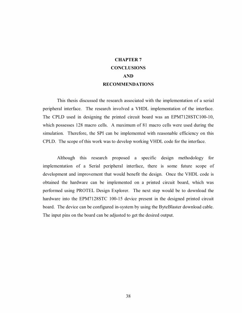
6.7 SPI Slave Figure 6.12 presents the waveforms generated by the SPI Slave. The complete
design is enabled only when an active low MSTR signal is present. The MOSI output of
the SPI slave component is the inverted input signal. The design utilized 7% of the area
of an EPM 7128STC100-10. Additionally, approximately 10 MACRO CELLS were
consumed.
Figure 6.12. Output of the SPI Slave
38
CHAPTER 7
CONCLUSIONS
AND
RECOMMENDATIONS
This thesis discussed the research associated with the implementation of a serial
peripheral interface. The research involved a VHDL implementation of the interface.
The CPLD used in designing the printed circuit board was an EPM7128STC100-10,
which possesses 128 macro cells. A maximum of 81 macro cells were used during the
simulation. Therefore, the SPI can be implemented with reasonable efficiency on this
CPLD. The scope of this work was to develop working VHDL code for the interface.
Although this research proposed a specific design methodology for
implementation of a Serial peripheral interface, there is some future scope of
development and improvement that would benefit the design. Once the VHDL code is
obtained the hardware can be implemented on a printed circuit board, which was
performed using PROTEL Design Explorer. The next step would be to download the
hardware into the EPM7128STC 100-15 device present in the designed printed circuit
board. The device can be configured in-system by using the ByteBlaster download cable.
The input pins on the board can be adjusted to get the desired output.

39
REFERENCES
[1] ALTERA, QuartusII VHDL, San Jose, Altera, 1996
[2] “SPI - Serial Peripheral Interface”, html files, http://www.mct.net/faq/spi.html
[3] Sooyong Lee, Jangwook Lee, Dae-Sung Choi, Munsang Kim and Chong-Won Lee,
“The Distributed Controller Architecture for a Masterarm and its Application to
Teleoperation with Force Feedback”, IEEE International Conference on Robotics &
Automation, May 1999
[4] Darold Wobschall and Hari Sai Prasad, “ESbus – A Sensor Bus Based on the SPI
Serial Interface”, IEEE International Conference
[5] Marco Faccio, Paolo Grande, Francesco Parasiliti, Roberto Petrella and Marco
Tursini, “An Embedded System for Position and Speed Measurement Adopting
Incremental Encoders”, IEEE International Conference, 2004
[6] ALTERA “In-System Programmability”, pdf files, http://www.altera.com/
literature/an/an095.pdf
[7] ALTERA “MAX 7000 Programmable Logic Device Family”, pdf files,
http://www.altera.com/literature/ds/m7000.pdf
[8] ALTERA “MAX Configuring Mercury, APEX 20K (2.5 V), ACEX 1K & FLEX
10K Devices”, pdf files, http://www.altera.com/literature/hb/cfg/cfg_cf51005.pdf
[9] “Configuration devices”, http://www.altera.com/literature/hb/cyc/cyc_c5v1_06.pdf

40
[10] “Quartus tool”, http://www.altera.com/literature/manual/intro_to_quartus2.pdf
[11] “Literature overview of ALTERA QuartusII Software”,
http://www.altera.com/literature/hb/qts/qts_qii54001.pdf
[12] ATmega 128(L) preliminary complete datasheet

41
APPENDICES
42
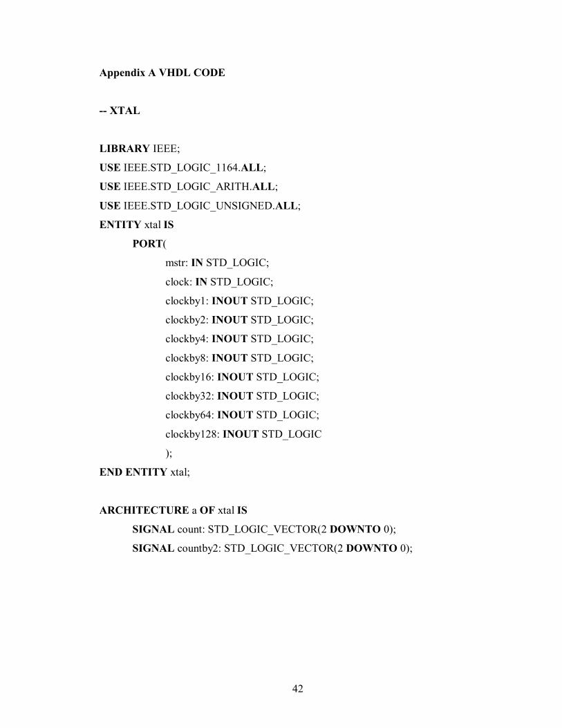
Appendix A VHDL CODE
-- XTAL
LIBRARY IEEE;
USE IEEE.STD_LOGIC_1164.ALL;
USE IEEE.STD_LOGIC_ARITH.ALL;
USE IEEE.STD_LOGIC_UNSIGNED.ALL;
ENTITY xtal IS
PORT(
mstr: IN STD_LOGIC;
clock: IN STD_LOGIC;
clockby1: INOUT STD_LOGIC;
clockby2: INOUT STD_LOGIC;
clockby4: INOUT STD_LOGIC;
clockby8: INOUT STD_LOGIC;
clockby16: INOUT STD_LOGIC;
clockby32: INOUT STD_LOGIC;
clockby64: INOUT STD_LOGIC;
clockby128: INOUT STD_LOGIC
);
END ENTITY xtal;
ARCHITECTURE a OF xtal IS
SIGNAL count: STD_LOGIC_VECTOR(2 DOWNTO 0);
SIGNAL countby2: STD_LOGIC_VECTOR(2 DOWNTO 0);
43
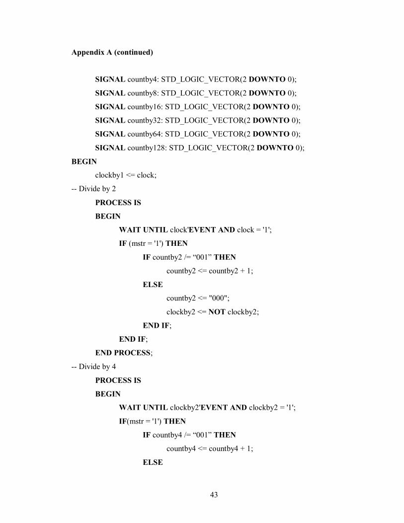
Appendix A (continued)
SIGNAL countby4: STD_LOGIC_VECTOR(2 DOWNTO 0);
SIGNAL countby8: STD_LOGIC_VECTOR(2 DOWNTO 0);
SIGNAL countby16: STD_LOGIC_VECTOR(2 DOWNTO 0);
SIGNAL countby32: STD_LOGIC_VECTOR(2 DOWNTO 0);
SIGNAL countby64: STD_LOGIC_VECTOR(2 DOWNTO 0);
SIGNAL countby128: STD_LOGIC_VECTOR(2 DOWNTO 0);
BEGIN
clockby1 <= clock;
-- Divide by 2
PROCESS IS
BEGIN
WAIT UNTIL clock'EVENT AND clock = '1';
IF (mstr = '1') THEN
IF countby2 /= “001” THEN
countby2 <= countby2 + 1;
ELSE
countby2 <= "000";
clockby2 <= NOT clockby2;
END IF;
END IF;
END PROCESS;
-- Divide by 4
PROCESS IS
BEGIN
WAIT UNTIL clockby2'EVENT AND clockby2 = '1';
IF(mstr = '1') THEN
IF countby4 /= “001” THEN
countby4 <= countby4 + 1;
ELSE
44
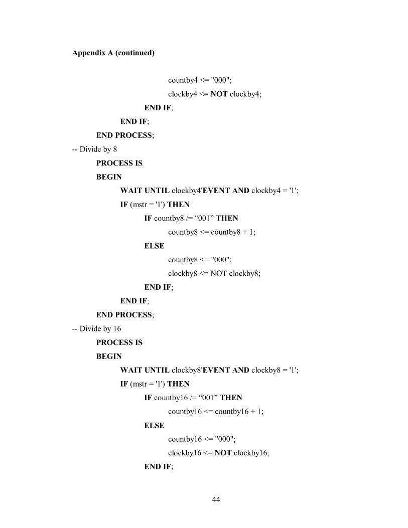
Appendix A (continued)
countby4 <= "000";
clockby4 <= NOT clockby4;
END IF;
END IF;
END PROCESS;
-- Divide by 8
PROCESS IS
BEGIN
WAIT UNTIL clockby4'EVENT AND clockby4 = '1';
IF (mstr = '1') THEN
IF countby8 /= “001” THEN
countby8 <= countby8 + 1;
ELSE
countby8 <= "000";
clockby8 <= NOT clockby8;
END IF;
END IF;
END PROCESS;
-- Divide by 16
PROCESS IS
BEGIN
WAIT UNTIL clockby8'EVENT AND clockby8 = '1';
IF (mstr = '1') THEN
IF countby16 /= “001” THEN
countby16 <= countby16 + 1;
ELSE
countby16 <= "000";
clockby16 <= NOT clockby16;
END IF;

45
Appendix A (continued)
END IF;
END PROCESS;
-- Divide by 32
PROCESS IS
BEGIN
WAIT UNTIL clockby16'EVENT AND clockby16 = '1';
IF (mstr = '1') THEN
IF countby32 /= “001” THEN
countby32 <= countby32 + 1;
ELSE
countby32 <= "000";
clockby32 <= NOT clockby32;
END IF;
END IF;
END PROCESS;
-- Divide by 64
PROCESS IS
BEGIN
WAIT UNTIL clockby32'EVENT AND clockby32 = '1';
IF (mstr = '1') THEN
IF countby64 /= “001” THEN
countby64 <= countby64 + 1;
ELSE
countby64 <= "000";
clockby64 <= NOT clockby64;
END IF;
END IF;
END PROCESS;
-- Divide by 128

46
Appendix A (continued)
PROCESS IS
BEGIN
WAIT UNTIL clockby64'EVENT AND clockby64 = '1';
IF (mstr = '1') THEN
IF countby128 /= “001” THEN
countby128 <= countby128 + 1;
ELSE
countby128 <= "000";
clockby128 <= NOT clockby128;
END IF;
END IF;
END PROCESS;
END ARCHITECTURE a;
-- PIN CONTROL LOGIC
LIBRARY IEEE;
USE IEEE.STD_LOGIC_1164.ALL;
USE IEEE.NUMERIC_STD.ALL;
ENTITY pin_cl IS
PORT(
mstr: IN STD_LOGIC;
spe: IN STD_LOGIC;
dord: IN STD_LOGIC;
adbus: IN STD_LOGIC_VECTOR(7 DOWNTO 0);
adbuf: OUT STD_LOGIC_VECTOR(7 DOWNTO 0);
;
END ENTITY pin_cl;

47
Appendix A (continued)
ARCHITECTURE data OF pin_cl IS
BEGIN
PROCESS (mstr,spe) IS
BEGIN
IF (mstr = '1') THEN
IF (spe = '1') THEN
IF (dord = '1')THEN
adbuf (7 DOWNTO 0) <= adbus(7 DOWNTO 0);
ELSIF(dord = '0') THEN
adbuf (7) <= adbus(0);
adbuf (6) <= adbus(1);
adbuf (5) <= adbus(2);
adbuf (4) <= adbus(3);
adbuf (3) <= adbus(4);
adbuf (2) <= adbus(5);
adbuf (1) <= adbus(6);
adbuf (0) <= adbus(7);
END IF;
END IF;
END IF;
END PROCESS;
END ARCHITECTURE data;
-- RECEIVE SHIFT REGISTER
LIBRARY IEEE;
USE IEEE.STD_LOGIC_1164.ALL;
USE IEEE. STD_LOGIC_ARITH.ALL;
ENTITY rcv_shift_reg IS
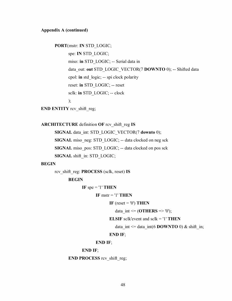
48
Appendix A (continued)
PORT(mstr: IN STD_LOGIC;
spe: IN STD_LOGIC;
miso: in STD_LOGIC; -- Serial data in
data_out: out STD_LOGIC_VECTOR(7 DOWNTO 0); -- Shifted data
cpol: in std_logic; -- spi clock polarity
reset: in STD_LOGIC; -- reset
sclk: in STD_LOGIC; -- clock
);
END ENTITY rcv_shift_reg;
ARCHITECTURE definition OF rcv_shift_reg IS
SIGNAL data_int: STD_LOGIC_VECTOR(7 downto 0);
SIGNAL miso_neg: STD_LOGIC; -- data clocked on neg sck
SIGNAL miso_pos: STD_LOGIC; -- data clocked on pos sck
SIGNAL shift_in: STD_LOGIC;
BEGIN
rcv_shift_reg: PROCESS (sclk, reset) IS
BEGIN
IF spe = '1' THEN
IF mstr = '1' THEN
IF (reset = '0') THEN
data_int <= (OTHERS => '0');
ELSIF sclk'event and sclk = '1' THEN
data_int <= data_int(6 DOWNTO 0) & shift_in;
END IF;
END IF;
END IF;
END PROCESS rcv_shift_reg;
49
Appendix A (continued)
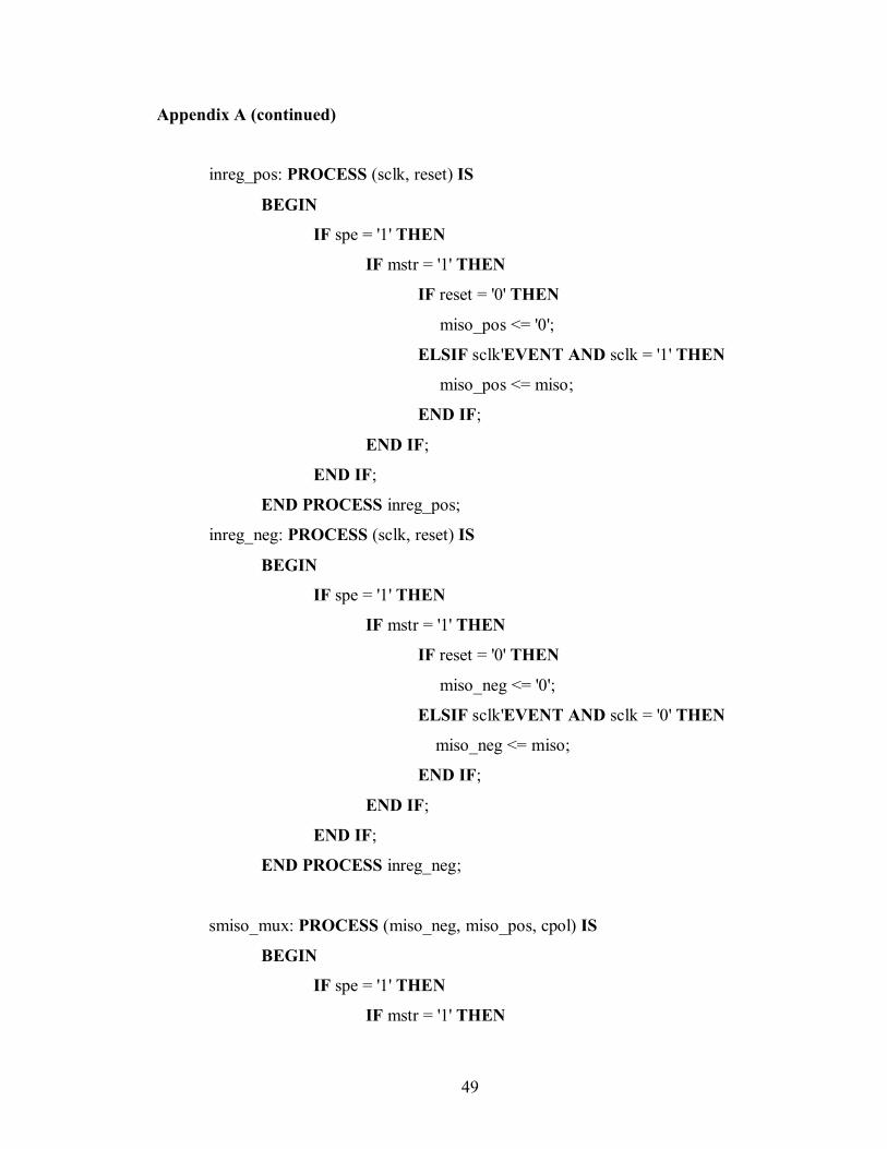
inreg_pos: PROCESS (sclk, reset) IS
BEGIN
IF spe = '1' THEN
IF mstr = '1' THEN
IF reset = '0' THEN
miso_pos <= '0';
ELSIF sclk'EVENT AND sclk = '1' THEN
miso_pos <= miso;
END IF;
END IF;
END IF;
END PROCESS inreg_pos;
inreg_neg: PROCESS (sclk, reset) IS
BEGIN
IF spe = '1' THEN
IF mstr = '1' THEN
IF reset = '0' THEN
miso_neg <= '0';
ELSIF sclk'EVENT AND sclk = '0' THEN
miso_neg <= miso;
END IF;
END IF;
END IF;
END PROCESS inreg_neg;
smiso_mux: PROCESS (miso_neg, miso_pos, cpol) IS
BEGIN
IF spe = '1' THEN
IF mstr = '1' THEN

50
Appendix A (continued)
IF cpol = '1' THEN
shift_in <= miso_pos;
ELSE
shift_in <= miso_neg;
END IF;
END IF;
END IF;
END PROCESS smiso_mux;
d-out: PROCESS (DATA_INT) IS
BEGIN
IF spe = '1' THEN
IF mstr = '1' THEN
data_out <= data_int(6 DOWNTO 0) & shift_in;
END IF;
END IF;
END PROCESS d-out;
END ARCHITECTURE definition;
-- CLOCK LOGIC
LIBRARY IEEE;
USE IEEE.STD_LOGIC_1164.ALL;
USE IEEE.STD_LOGIC_ARITH.ALL;
ENTITY sck_logic IS
PORT(mstr: IN STD_LOGIC;
enable: IN STD_LOGIC;
SPI2X: IN STD_LOGIC;
SPR1: IN STD_LOGIC;

51
Appendix A (continued)
SPR0: IN STD_LOGIC;
cpha: IN STD_LOGIC;
cpol: IN STD_LOGIC;
sck: INOUT STD_LOGIC;
clk: IN STD_LOGIC
);
END ENTITY sck_logic;
ARCHITECTURE definition OF sck_logic IS
SIGNAL clk_cnt: STD_LOGIC_VECTOR(7 downto 0);
SIGNAL sck_int: STD_LOGIC;
SIGNAL sck_0: STD_LOGIC;
SIGNAL sck_out: STD_LOGIC;
SIGNAL clkdiv: STD_LOGIC_VECTOR(2 DOWNTO 0);
COMPONENT xtal IS
PORT(mstr: IN STD_LOGIC;
clock: IN STD_LOGIC;
clockby1: INOUT STD_LOGIC;
clockby2: INOUT STD_LOGIC;
clockby4: INOUT STD_LOGIC;
clockby8: INOUT STD_LOGIC;
clockby16: INOUT STD_LOGIC;
clockby32: INOUT STD_LOGIC;
clockby64: INOUT STD_LOGIC;
clockby128: INOUT STD_LOGIC
);
END COMPONENT xtal;
BEGIN

52
Appendix A (continued)
clkdiv <= SPI2X & SPR1 &SPR0;
clk_DIVDR: xtal PORT MAP (mstr=> mstr, clock => clk, clockby1 =>
clk_cnt(0), clockby2 => clk_cnt(1), clockby4 => clk_cnt(2),
clockby8 => clk_cnt(3), clockby16 => clk_cnt(4), clockby32 =>
clk_cnt(5), clockby64 => clk_cnt(6), clockby128 => clk_cnt(7));
sck_int_process: PROCESS (clk, enable) IS
BEGIN
IF mstr = '1' THEN
IF enable = '0' THEN
sck_int <= '0';
ELSIF clk'EVENT AND clk = '1' THEN
CASE clkdiv IS
WHEN "000" => sck_int <= clk_cnt(2);
WHEN "001" => sck_int <= clk_cnt(4);
WHEN "010" => sck_int <= clk_cnt(6);
WHEN "011" => sck_int <= clk_cnt(7);
WHEN "100" => sck_int <= clk_cnt(1);
WHEN "101" => sck_int <= clk_cnt(3);
WHEN "110" => sck_int <= clk_cnt(5);
WHEN "111" => sck_int <= clk_cnt(6);
WHEN OTHERS => sck_int <= '0';
END CASE;
END IF;
END IF;
END PROCESS sck_int_process;
sck_0_process: PROCESS (clk, enable) IS
BEGIN
IF mstr = '1' THEN

53
Appendix A (continued)
IF enable = '0' THEN
sck_0 <= '0';
ELSIF clk'EVENT AND clk = '1' THEN
CASE clkdiv IS
WHEN "000" => sck_0 <= NOT(clk_cnt(2));
WHEN "001" => sck_0 <= NOT (clk_cnt(4));
WHEN "010" => sck_0 <= NOT (clk_cnt(6));
WHEN "011" => sck_0 <= NOT (clk_cnt(7));
WHEN "100" => sck_0 <= NOT (clk_cnt(1));
WHEN "101" => sck_0 <= NOT (clk_cnt(3));
WHEN "110" => sck_0 <= NOT (clk_cnt(5));
WHEN "111" => sck_0 <= NOT (clk_cnt(6));
WHEN OTHERS => sck_0 <= '0';
END CASE;
END IF;
END IF;
END PROCESS sck_0_process;
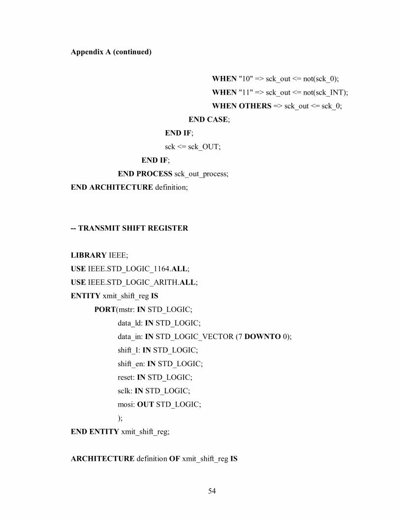
sck_out_process: PROCESS (clk, enable, cpol) IS
VARIABLE temp: STD_LOGIC_VECTOR (1 DOWNTO 0);
BEGIN
IF mstr ='1' THEN
IF enable = '0' THEN
sck_out <= '0';
ELSIF clk'EVENT AND clk = '1' THEN
temp := cpol & cpha;
CASE temp is
WHEN "00" => sck_out <= sck_0;
WHEN "01" => sck_out <= sck_INT;
54
Appendix A (continued)
WHEN "10" => sck_out <= not(sck_0);
WHEN "11" => sck_out <= not(sck_INT);
WHEN OTHERS => sck_out <= sck_0;
END CASE;
END IF;
sck <= sck_OUT;
END IF;
END PROCESS sck_out_process;
END ARCHITECTURE definition;
-- TRANSMIT SHIFT REGISTER
LIBRARY IEEE;
USE IEEE.STD_LOGIC_1164.ALL;
USE IEEE.STD_LOGIC_ARITH.ALL;
ENTITY xmit_shift_reg IS
PORT(mstr: IN STD_LOGIC;
data_ld: IN STD_LOGIC;
data_in: IN STD_LOGIC_VECTOR (7 DOWNTO 0);
shift_I: IN STD_LOGIC;
shift_en: IN STD_LOGIC;
reset: IN STD_LOGIC;
sclk: IN STD_LOGIC;
mosi: OUT STD_LOGIC;
);
END ENTITY xmit_shift_reg;
ARCHITECTURE definition OF xmit_shift_reg IS

55
Appendix A (continued)
CONSTANT reset_ACTIVE: STD_LOIC:= '0';
SIGNAL data_int: STD_LOGIC_VECTOR (7 DOWNTO 0);
SIGNAL mosi_int: STD_LOGIC;
BEGIN
xmit_shift_reg: PROCESS (sclk, reset) IS
BEGIN
IF mstr = '1' THEN
-- Clear output register
IF (reset = '0') THEN
data_int <= (OTHERS => '0');
-- On rising edge of spi clock, shift data
ELSIF sclk'EVENT AND sclk = '1' THEN
-- Load data
IF (data_ld = '1') THEN
data_int <= data_in;
-- If shift enable is high
ELSIF shift_en = '1' THEN
-- Shift the data
data_int <= data_int(6 DOWNTO 0) & shift_in;
END IF;
END IF;
END IF;
END PROCESS xmit_shift_reg;
outreg: PROCESS (sclk, reset) IS
BEGIN
IF mstr = '1' THEN
IF reset = reset_ACTIVE THEN
mosi_int <= '0';

56
Appendix A (continued)
ELSIF sclk'EVENT AND sclk = '1' THEN
mosi_int <= data_int(7);
END IF;
mosi <= mosi_int;
END IF;
END PROCESS;
END ARCHITECTURE definition;
-- SPI MASTER
LIBRARY IEEE;
USE IEEE.STD_LOGIC_1164.ALL;
USE IEEE.NUMERIC_STD.ALL;
ENTITY spi_master IS
PORT(DATALOAD: INOUT STD_LOGIC; -- LOAD DATA
enable: IN STD_LOGIC; -- system enable
xtal: IN STD_LOGIC; -- INPUT clock
spe: IN STD_LOGIC; -- SET TO 1 FOR ALL SPI OPERATIONS
dord: IN STD_LOGIC; -- THE ORDERDATA IS SENT OUT
mstr: IN STD_LOGIC; -- SPI ACTS AS MASTER OR SLAVE
cpol: IN STD_LOGIC; -- POLARITY OF clock
cpha: IN STD_LOGIC; -- PHASE OF clock
SPR1: IN STD_LOGIC; -- 2ND BIT FOR clock FREQ
SPR0: IN STD_LOGIC; -- 1ST BIT FOR clock FREQ
SPI2X: IN STD_LOGIC; -- 3RD BIT FOR clock FREQ
miso: IN STD_LOGIC; -- SLAVE OUT MASTER IN
sck: OUT STD_LOGIC; -- SYSTEM OUTPUT clock
SS: OUT STD_LOGIC; -- SLAVE enable
57
Appendix A (continued)
mosi: OUT STD_LOGIC; -- MASTER OUT SLAVE IN
adbuf: OUT STD_LOGIC_VECTOR(7 DOWNTO 0);
);
END ENTITY spi_master;
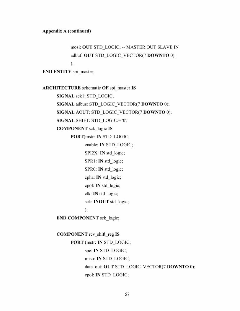
ARCHITECTURE schematic OF spi_master IS
SIGNAL sck1: STD_LOGIC;
SIGNAL adbus: STD_LOGIC_VECTOR(7 DOWNTO 0);
SIGNAL AOUT: STD_LOGIC_VECTOR(7 DOWNTO 0);
SIGNAL SHIFT: STD_LOGIC:= '0';
COMPONENT sck_logic IS
PORT(mstr: IN STD_LOGIC;
enable: IN STD_LOGIC;
SPI2X: IN std_logic;
SPR1: IN std_logic;
SPR0: IN std_logic;
cpha: IN std_logic;
cpol: IN std_logic;
clk: IN std_logic;
sck: INOUT std_logic;
);
END COMPONENT sck_logic;
COMPONENT rcv_shift_reg IS
PORT (mstr: IN STD_LOGIC;
spe: IN STD_LOGIC;
miso: IN STD_LOGIC;
data_out: OUT STD_LOGIC_VECTOR(7 DOWNTO 0);
cpol: IN STD_LOGIC;
58
Appendix A (continued)
reset: IN STD_LOGIC;
sclk: IN STD_LOGIC;
);
END COMPONENT rcv_shift_reg;
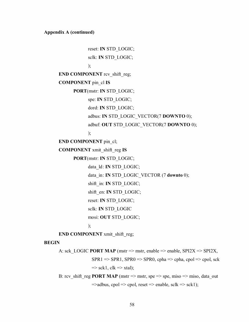
COMPONENT pin_cl IS
PORT(mstr: IN STD_LOGIC;
spe: IN STD_LOGIC;
dord: IN STD_LOGIC;
adbus: IN STD_LOGIC_VECTOR(7 DOWNTO 0);
adbuf: OUT STD_LOGIC_VECTOR(7 DOWNTO 0);
);
END COMPONENT pin_cl;
COMPONENT xmit_shift_reg IS
PORT(mstr: IN STD_LOGIC;
data_ld : IN STD_LOGIC;
data_in : IN STD_LOGIC_VECTOR (7 downto 0);
shift_in: IN STD_LOGIC;
shift_en: IN STD_LOGIC;
reset: IN STD_LOGIC;
sclk: IN STD_LOGIC
mosi: OUT STD_LOGIC;
);
END COMPONENT xmit_shift_reg;
BEGIN
A: sck_LOGIC PORT MAP (mstr => mstr, enable => enable, SPI2X => SPI2X,
SPR1 => SPR1, SPR0 => SPR0, cpha => cpha, cpol => cpol, sck
=> sck1, clk => xtal);
B: rcv_shift_reg PORT MAP (mstr => mstr, spe => spe, miso => miso, data_out
=>adbus, cpol => cpol, reset => enable, sclk => sck1);
59
Appendix A (continued)
C: pin_cl PORT MAP (mstr => mstr, spe => spe, dord => dord, adbus => adbus,
adbuf => AOUT);
D: xmit_shift_reg PORT MAP (mstr => mstr, data_ld => DATALOAD, data_in
=> AOUT, shift_in => miso, shift_en => enable, mosi=>mosi,
reset => enable, sclk => sck1);
sck <= sck1;
adbuf <= AOUT;
END ARCHITECTURE schematic;
SPI SLAVE
LIBRARY IEEE;
USE IEEE.STD_LOGIC_1164.ALL;
USE IEEE.NUMERIC_STD.ALL;
ENTITY spi_slave IS
PORT(DATALOAD: INOUT STD_LOGIC; -- LOAD DATA
enable: IN STD_LOGIC; -- system enable
xtal: IN STD_LOGIC; -- INPUT clock
spe: IN STD_LOGIC; -- SET TO 1 FOR ALL SPI OPERATIONS
dord: IN STD_LOGIC; -- THE ORDERDATA IS SENT OUT
mstr: IN STD_LOGIC; -- SPI ACTS AS MASTER OR SLAVE
cpol: IN STD_LOGIC; -- POLARITY OF clock
cpha: IN STD_LOGIC; -- PHASE OF clock
SPR1: IN STD_LOGIC; -- 2ND BIT FOR clock FREQ
SPR0: IN STD_LOGIC; -- 1ST BIT FOR clock FREQ
SPI2X: IN STD_LOGIC; -- 3RD BIT FOR clock FREQ
mosi: IN STD_LOGIC; -- MASTER OUT SLAVE IN
sck: IN STD_LOGIC; -- SYSTEM OUTPUT clock
SS: IN STD_LOGIC; -- SLAVE enable

60
Appendix A (continued)
adbuf: OUT STD_LOGIC_VECTOR(7 DOWNTO 0)
miso: OUT STD_LOGIC; -- SLAVE OUT MASTER IN
);
END ENTITY spi_slave;
ARCHITECTURE beh OF spi_slave IS
SIGNAL ADIN: STD_LOGIC_VECTOR(7 DOWNTO 0);
BEGIN
PROCESS (mosi, sck) IS
BEGIN
IF spe = '1' THEN
IF mstr = '0' THEN
IF sck'EVENT AND sck = '1' THEN
miso <= NOT(mosi);
END IF;
IF sck'EVENT AND sck = '1' THEN
adbuf <= ADIN(6 DOWNTO 0) & mosi;
END IF;
END IF;
END IF;
END PROCESS;
END ARCHITECTURE beh;