a design analysis of a hybrid technology multithreaded
TRANSCRIPT
Submitted to International Conference onSupercomputing (ICS'99), Rhodes, Greece
June 20-25, 1999 - 1 -
A Design Analysis of a Hybrid Technology Multithreaded Architecturefor Petaflops Scale Computation
Thomas Sterling and Larry BergmanJet Propulsion Laboratory
California Institute of TechnologyPasadena, California
ABSTRACT
Petaflops scale computing may be feasible within the next five to seven years through a mix of emerginginnovative device technologies. Important advances in the fields of superconductor logic, opticalcommunications and storage, and processor-in-memory (PIM) semiconductor fabrication are yielding dramaticimprovements in speed, power consumption, and parts count with respect to conventional device technologies.The Hybrid-Technology Multithreaded (HTMT) parallel computer architecture has been developed to addressthe challenges of incorporating these new devices in an effective computing system. HTMT employs proactivelatency management and parallel task scheduling mechanisms enabled by PIM DRAM and SRAM to eliminatemost long access delays and overhead operations by the very high speed processors, thus providing highprocessor efficiency. A two year research project conducted by a dozen institutions and sponsored by four USFederal agencies has developed and investigated the HTMT architecture and its design space tradeoffs. Thedetailed quantitative findings of this interdisciplinary study have demonstrated the viability of implementing apetaflops scale HTMT computing system as early as 2004. This paper is the first formal presentation of theinterim findings of the HTMT research project and describes the HTMT architecture with its enablingtechnologies including in-depth quantitative analysis of its size, power, and complexity characteristics.
1. INTRODUCTION
Even as Teraflops scale systems are becoming available for a few high priority applications of nationalinterest, experts across diverse fields in engineering and the sciences have identified a multiplicity ofimportant applications that require far greater capability, on the scale of a petaflops. Teraflops scalemassively parallel processors (MPPs) are being implemented in CMOS technology at a cost ofapproximately 100 million dollars and power consumption of megawatts. Direct scaling of thesetechnologies to the petaflops regime would be prohibitive in cost, power consumption, and size. Estimatesof when such performance would be feasible relying on incremental semiconductor advances andconventional MPP system architecture range from the year 2010 to 2015. But even then, importantadvances in semiconductor lithography and fabrication would be required with no promise of the means ofmaking efficient use of such resources when available. For those important applications already requiringsuch throughput, the prospects based on conventional strategies in the near term are not favorable.
Historically, the evolution of computer system design has been marked by dramatic gains in performanceand price-performance enabled by advanced device technologies combined with innovative concepts incomputer architecture. Mainframes, vector supercomputers, and MPPs have each represented a distinctsynergism of device technology, system organization, and execution model. While the MPP strategyapproaches maturity, a new opportunity is emerging in a set of device technologies and architectureprinciples that may make possible petaflops scale systems in five to seven years instead of ten to fifteenyears [8]. These technologies include advanced Silicon-Germanium and superconductor logic, opticalcommunications, holographic optical storage, and processor-in-memory DRAM. Task and latencymanagement architecture concepts based on advanced multithreaded execution models provide a means fororganizing these and other possible technologies to derive a possible next stage in high end computersystem implementation. A major research project has been conducted to develop and evaluate a hybridtechnology multithreaded (HTMT) architecture incorporating advanced devices and employing proactiveruntime adaptive latency management mechanisms.
This paper is the first formal presentation of the findings of the ambitious HTMT study [4, 5] and reportson the feasibility of achieving petaflops in a few years by harnessing these advanced technologies. Adetailed quantitative analysis is provided that determines the size, complexity, cost, power consumption,

- 2 -
and operational parameters of the HTMT system and its constituent elements capable of being implementedin the year 2004. The next section of this paper discusses the key constraints restricting achievableperformance and describes the strategy embodied by the HTMT architecture to address each of these.Section 3 presents a description of each of the enabling technologies and their operational characteristics.Section 4 describes the HTMT architecture with a brief discussion of the task and latency managementexecution model. Section 5 provides the principle quantitative results of this work giving a detailedspecification of the structure, size, complexity, and power consumption of an HTMT based petaflopscomputer in 2004. Finally, Section 6 concludes with a discussion of the greatest challenges toaccomplishing petaflops computing by means of the methods described as well as a brief outline of futurework leading to a small test prototype.
2. APPROACH
The objectives of the HTMT project are to develop a scalable architecture with high sustained performancein the presence of disparate cycle times and latencies in order to exploit diverse device technologies withsuperior properties and to incorporate an execution model that simplifies parallel system programmingwhile expanding generality and applicability. Realization of a very high performance computing systemwill simultaneously address a number of critical constraints to practical implementation. Any credibleapproach to high end computer architecture must include a strategy that compensates for the challenges of:
• Aggregating sufficient computing resources to achieve the necessary peak performance,
• Incorporating sufficient data storage capacity and memory bandwidth,
• Constraining system manufacture costs to within market tolerance,
• Limiting power consumption including cooling within practical bounds,
• Managing latency, task supervision overhead, and resource contention delays for high efficiency andsustained performance, and
• Providing programmability and generality for wide applicability and ease of use.
The HTMT architecture (Fig. 1) addresses all of these through a combination of device technology andarchitecture innovation. Peak performance is accomplished by use of superconductor rapid single fluxquantum (RSFQ) logic which will enable local clock rates of greater than 100 GHz. Additionalperformance is gained by a large number of small processors embedded in the main memory itself that arewell suited for various data intensive operations. Data storage capacity is achieved by augmentingsemiconductor DRAM technology with high density holographic photo-refractive storage.
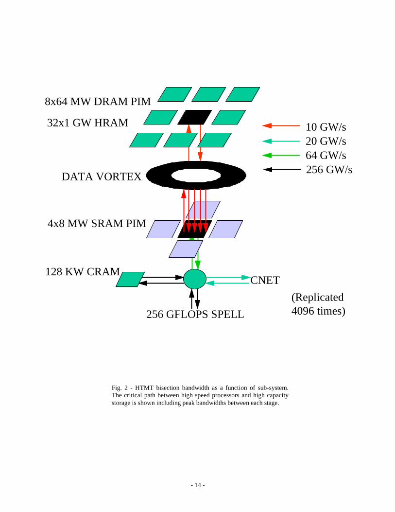
Memory bandwidth (Fig. 2) is achieved in several ways. Operations performed internally to the memorychips using PIM technology have direct access to the memory row buffers and can operate on all bitssimultaneously within one DRAM memory cycle. While exhibiting a longer access time, the holographicstorage acquires a megabit page at a time yielding very high bandwidth. And the Data Vortex opticalcommunication network exploits both TDM and WDM encoding to achieve hundreds of gigabits persecond per fiber. To the extent that cost is a function of system complexity and parts count, by usingtechnologies with very high throughput and capacities, fewer parts are required for a given performancecapability.
Power consumption is one of the most important challenges and is addressed, again, through a mix oftechnologies. The superconductor RSFQ technology, in spite of its need for refrigeration, consumes lessthan one percent of the power required for conventional technologies delivering comparable performance.PIM technology consumes about one tenth the power of conventional approaches because of its efficientuse of on-chip memory bandwidth. Holographic storage also requires much less power per bit than

- 3 -
conventional memory. The Data Vortex optical network employs much less power for a given bandwidththan would be required by conventional wire based carriers.
Efficiency is determined by a number of factors including access latency, overhead of task management,contention for shared physical resources, and starvation due to insufficient work to keep all parallelprocessors busy. The HTMT system architecture addresses these performance inhibiting factors by adistributed runtime strategy of task management and latency hiding using advanced multithreadedmechanisms implemented in both the high speed processors and smart PIM memories. Latencies of up to afew hundred cycles are hidden my supporting multiple concurrent active threads and their local state withinthe high speed processors and switching among any pair of them within a single cycle. A second level oftask management is handled by the smart cache SRAM PIM and the main memory DRAM PIM layers,migrating pending processes to the SRAM while moving suspended processes to the DRAM.
More efficiency is achieved by performing some operations in-place on the data in memory where spatialand temporal locality do not warrant processor action. Gather/scatter operations and traversal of irregularpointer-linked data structures are thus efficiently performed. Memory to memory data movement can beaccomplished, again without processor intervention.
Both programmability and generality of application are enhanced with respect to MPP oriented practices bygreatly reducing the direct resource management responsibilities of the programmer and providingarchitecture supported runtime mechanisms for adaptive resource management. A single global memoryname space is employed as opposed to the fragmented memory blocks found on many MPPs. The"percolation" method of migrating ready tasks from the memory to the smart cache and dynamically loadbalancing across the array of high speed processors, again eliminates programmer intervention.
The overall target specifications of the HTMT system are shown in the Table 1 below. The latency refers tothe number of clock cycles a processor must wait (one way) to access that memory system. More detail ofeach of the HTMT component parts and specifications will be described in the following sections.
3. ENABLING TECHNOLOGIES
A set of breakthrough technologies has been identified that may greatly accelerate performance of high endcomputing. The particular strengths of each complement the others to deliver dramatic improvements inperformance, storage capacity, bisection bandwidth, and power consumption. A brief description of the key
Sub-SystemElement
PartsCount
TotalSize
I/O Bandwidth(B/s)
Latency(PE cycles)
PEs 4096 pes 1 PFLOP/s 1.2-12 PB/s -
CRAM 16K ics 512 MB 8 PB/s 70
SRAM 16K ics 1 TB 4 PB/s 240
Optical Net 372K nodes 6250 ports 640 TB/s 10K
DRAM 32K ics 16 TB 320 TB/s 16K
HRAM 128K ics 1 PB 320 TB/s 67K
Disk 100K-1M 10PB-100PB 1 TB/s - 10 TB/s 100G
Tape- robots- transports
20-200250-2500
100PB - 1EB 24 GB/s - 240 GB/s -
Table 1 - HTMT Target Specifications

- 4 -
technologies being considered by the HTMT research project follows. Other technologies, not presenteddue to space limitations, are also being considered as possible alternatives.
3.1 Superconductor Digital Electronics
The potential of superconductor electronics for high speed digital computing has been pursued since the1970s but until this decade the speed advantages were insufficient to warrant extensive investment. Earlycircuit designs mirrored digital circuit design of conventional transistor based logic gates delivering clockrates between 1 and 3 GHz. The development of the single flux quantum circuit using two Josephsonjunctions (JJ's) and an inductor created an alternative building block from which to devise digital logic.Enhancement of this approach provided rapid single flux quantum (RSFQ) logic with demonstrated clockrates for small circuits of 750 GHz and the potential for chip-wide clock speeds of 100 GHz or more [7, 9,10]. Figure 3 shows two road maps of projected clock speeds [7]. The lower curve presents those takenfrom the SIA projections for CMOS technology while the upper curve is for Niobium based RSFQ logicover the same time period. It is clear that RSFQ technology will retain a two order of magnitude advantagein switching rate for the next decade.
Modest sized RSFQ chips of 1.5 to 2.5 micron feature size are routinely fabricated for military andindustrial application incorporating a few thousands of gates per chip at most. Devices of 0.8 micronNiobium technology has been demonstrated in the laboratory that should permit 100 GHz clock speeds onchips containing 100K gates. Smaller feature sizes have been achieved for a few select devices as well.Inter-chip data transfer rates within MCM packages can be realized up to 30 Gbps while rates of 10 Gbps isachieved between MCMs.
A second property of superconductor RSFQ logic is its extraordinary low power consumption with respectto conventional CMOS technology. A gate operating at 100 GHz consumes 0.1 microwatts of power whichis more than four orders of magnitude less energy per logical operation than required by CMOS. Even withthe relatively inefficient refrigeration employed today to maintain the necessary cryogenic thermalenvironment for superconductivity, the power advantage is approximately a factor of a hundred.
3.2 Smart Memories
Semiconductor fabrication processes for logic and DRAM memory cells are significantly differentordinarily dictating that the two forms of functionality be implemented on separate integrated circuits. Thisdichotomy of manufacture methodology has perpetuated the separation of memory and processors referredto as the "von Neumann bottleneck." Recent advances in semiconductor processing has made possible themerger of logic and dynamic memory cells on the same die. Recent significant reduction in feature size andincrease in die size has made it possible to dedicate some of the once precious die real estate to logic whileretaining significant memory capacity.
Processor-in-memory or "PIM" technology [3, 16] offers a new dimension in computer system designproviding an important alternative to the conventional processor/memory relationship of the last 50 years.PIM technology puts logic directly at or near the sense amps of the DRAM cell stack (Fig. 4). A dataaccess cycle will acquire one entire row of the memory cell block at a time. Typically, this can be one ormore thousand bits every 50 to 150 nanoseconds or faster for particular smaller sub-blocks. Includingmultiple blocks per chip that are separately accessible and accessing only a sub-block of the total availablerow can deliver between 100 and 200 Gbps on-chip sustained memory bandwidth. Because logic is directlyconnected to the row buffers, processing of the data at this rate under favorable conditions is possible dueto the low latency interconnects on chip.
3.3 Optical Communication Network
Recent dramatic advances in optical communications technology offer the opportunity to implement systemarea networks (SAN) in optics for the first time [12, 13]. For next generation high end systems, total systemdata transfer rates may be required at hundreds of Terabits per second making use of electrical channelsprohibitive both in terms of number of wires required and the power consumed. Per channel bandwidth

- 5 -
(TDM, single wavelength on a given fiber) is now feasible at 10 Gbps with the possibility of extending thisby more than a factor of two in the next few years. More significant is the rapid developments in wavedivision multiplexing (WDM). It is now possible to employ 64 wavelengths simultaneously on the samefiber with the prospect of 256 or more wavelengths likely within a few years. The combination of TDM andWDM techniques can provide between 32 Gbps and 640 Gbps per fiber within the next couple of yearswhile data rates in excess of a Tbps is envisioned in the not too distant future.
Routing of data packets among thousands of ports likely in very high end computer systems can requiredynamic switching of in-flight packets in a short period of time (Fig. 5). Contention arbitration and packetrouting through an optical network can be performed by a new generation of all-optical butterfly switchespassing the optical data payload of a packet directly through the switch without intervening conversion toelectrical and then back to optical. Only the packet header bits need be converted to electrical mode tocontrol switching. These new switches allow rapid, low power, low cost, network nodes to be employed inlarge networks. Recent advances in electro-optic integration make possible multiple switching nodes on asingle silicon substrate with direct fiber optic connectors. Nonlinear optical fiber loop mirror (NOLM)technology provide an all-optical data amplifier and cleaner to regenerate data as a result of power splittingoccurring in the switch nodes. The combination of these technologies makes optical system area networksboth feasible and advantageous for future high end computers.
3.4 Holographic 3/2 Memory
Holographic encoding of information has been understood for many decades but only recently has the useof such methods been employed for computer data storage and retrieval, principally for read only or write-once archival storage. Major advances in this field in the last few years has created new opportunities inhigh density low power storage [1, 2]. A planar spatial light modulator (SLM) forms an image of the datawhich produces a hologram in a layer of photo refractive material (Fig. 6). Later, a laser beam of the samewavelength and angle incident on the material will return the original data. Blocks of data of 1 to 4 Mbitscan be stored or retrieved at one time. The rate at which data can be accessed is a function of the propertiesof the selector mechanism. The primary application for this technology has been to augment secondarystorage permitting access time of a few milliseconds which could be achieved with mechanical deflectionschemes. For use as a supplement to main memory, access times on the order of 10 microseconds or ahundred times faster is required. The likely approach is to incorporate a laser array such as a laser diodearray or a Vertical Cavity Surface Emitting Laser (VCSEL) array combined with a lens to enable rapidpage access simply by activating different lasers within the array.
4. ARCHITECTURE
The general approach, strategy, and justification for the HTMT system architecture and its operation werediscussed in Section 2. Here, a summary of the system organization and the operational responsibilities ofeach of its comprising sub-elements is presented. The HTMT architecture may be viewed as an array ofvery high performance, low power processors driven by an intelligent memory hierarchy that supplies theprocessor array with a continuous stream of work and data, as shown in Figure 7. An alternativeperspective is that the HTMT system is made up of the high performance low power processor array and ahigh capacity low power holographic memory array which are coupled and matched by means of anintervening system buffer management and communication subsystem, as shown in Figure 8. In eitherview, the HTMT architecture revolutionizes the relationship between memory and processors, reversing theroles of master and slave. Low cost processors near the memory (in the smart cache and DRAM) performthe low efficiency overhead functions of organizing, synchronizing, scheduling, and moving tasks and databetween the high capacity storage and the high performance processors. The HTMT system structure isshown in Figure 1.
4.1 High Performance Processor
The processor architecture [6] is based on a simple multithreaded organization with a separate register bankdedicated to each thread of control (Fig. 9). The thread managers operate independently issuing instructions

- 6 -
with operands and fetching data and instructions from the high-speed memory buffers. Each processorincludes between 2 and 6 pipelined floating-point units. A group of thread managers share a pipelinedinteger unit. The number of thread managers per processor depends on a number of factors and isdetermined by the average amount of processor latency that must be overcome. Each processor is providedwith high speed buffer memory that takes the place of cache but is explicitly managed under programcontrol. Each processor and its buffer memory is directly connected to one bank of the highest speedmemory within the memory hierarchy. The processors are interconnected among themselves by the CNET,a high bandwidth Banyan network. Access to a specific bank of the memory hierarchy by a processor isthrough the C-net to the processor interface associated with the target bank. The use of ultra-fast logicimposes severe demands on processor structure [14, 15]. The dominant factors are:
Speed of light limitation: during a 10 ps. clock cycle (planned for the HTMT computer), a signalpropagating with the effective speed of light can only be passed over a 1mm distance, which is much lessthan the chip size necessary for petaflops-scale computing. In other words, this technology is relativistic:switching logic gates on the same chip are outside of each other's light cone.
Clock skew limitation: unless an extremely awkward and bulky hardware is used, clock skew across a fewcentimeter chip is comparable with or even larger than 10 ps. As a result, no global clock is practical, andcomputing even within one chip will be intrinsically asynchronous. In fact, the very notion of simultaneousevents loses meaning, unless the events happen within a small local area.
These two features of RSFQ circuits make a pipelined organization and RISC-like instruction setarchitecture (ISA) the natural design choices for the RSFQ subsystem. An ultra-small clock cycle andpipelines with negligible hardware cost for latches provide an efficient way to achieve the planned ultra-high performance. However, both the pipeline and the RISC ISA concepts should be revised to reflectchallenges imposed by the RSFQ technology. These challenges are:
• Small depth of each pipeline stage (ultimately, one level of logic).• Comparable time for processing within one pipeline stage and communication among adjacent pipeline
stages.
The first feature makes very long RSFQ pipelines unavoidable, while the second makes globalsynchronized communication within such pipelines impossible. The main problem to be solved is how toresolve data and control hazards for data paths. Very long pipelines and a lack of global synchronizationmake traditional approaches like data forwarding inapplicable for resolving data hazards. For the samereasons, speculative execution would be difficult to implement.
4.2 Smart Cache
The smart cache is a processor-in-memory part combining SRAM with a simple control processor. Eachbank of the smart cache serves in part as a backing store for the very high speed buffer memory related tothe associated processor. The smart cache also participates in the temporary high speed storage of the pagesof data currently being accessed by one or more of the processors. This layer of memory has two interfaces.Each bank of the smart cache has one interface to its corresponding processor in the processor array andone interface to the Data Vortex optical network. The Smart Cache participates in gather/scatter operationsand pointer chasing sequences without RSFQ processor intervention. It also engages in "percolation" toproactively pre-stage ready work for high speed processing.
4.3 PIM Main Memory
The main memory of the HTMT architecture is PIM based with several memory blocks and PIMprocessors per chip (Fig. 4). This PIM DRAM is internally multithreaded to support processing of one setof data while fetching another set from its local memory stack. The PIM chip is message driven. Packets,referred to as "parcels", acting in a manner similar to active messages may come from the high speedprocessors, the smart cache, or other main memory chips. These parcels, once dispatched, invoke a simpleoperation or small code fragment to carry out some task on stored data. The PIM main memory supports

- 7 -
two interfaces: one to the data vortex network connecting it to all other main memory chips and the smartcache, and the other interface connecting it to one of the holographic storage modules. The capacity of thePIM main memory chip depends on the technology in which it is implemented. Today, 0.25 micron partscan provide 8 to 16 megabytes of storage with processing logic.
4.4 Data Vortex Optical Network
The Data Vortex optical network and its opto-electronic subsystems are specifically designed to form thecommunications infrastructure between the SRAM and DRAM levels in the memory hierarchy [12]. Thenetwork employs multiple node levels with a routing topology that is based on a minimum logic at the nodescheme. This architecture is unique in its reduction of time-of-flight latency between communicationsports, with a network that is absolutely transparent and can scale to interconnect an ultra-high performancecomputing system in a massively parallel form.
In the Data Vortex topology (Fig. 10), the network nodes lie on a collection of concentric cylinders. Data isinjected into the outermost cylinder and emerges from the innermost cylinder. The data packets flowaround the cylinders on prescribed paths and drop from the larger outer cylinders to the smaller innercylinders. Each time that a packet drops down one cylinder, another bit of its target header is fixed. Thereare multiple paths between source and target, and the data flow is designed such that upon deflectionpackets will continuously drop into open paths. When a packet is deflected, it will be in a position toprogress toward its target in two clock cycles. That is, after bouncing through only two nodes, the packetrecovers its intended vector along another path. The packets on the smaller, inner cylinders haveprecedence over packets on the outer cylinders. In this way, the topology provides probabilistic preferenceto data that has been in the network longer. In order for the logic at a node to be kept to a minimumcontention resolution must be avoided. Therefore, the network was designed such that only one messagecan enter a node in a given clock cycle.
Control messages pass between nodes before the packet arrives at a given node, to establish the right ofway. Specifically, a node, A, on cylinder, C, has two input ports: one from a node B on the same cylinder,C and one from a node G on the cylinder one level higher than C. A message passing from B to A, causes asignal to be sent from B to G that blocks data at G from progressing to A. The network has no buffers,however the network itself acts as a buffer. Messages are never lost. If there is congestion at an outputbuffer, the data waiting to leave that buffer circulates around the lower cylinders and thus is optimallypositioned to exit immediately as soon as the output ports are free. The data payload of the packet is passedpurely optically; that is, there is no electro-optical conversion and therefore no active parts. As a result,latencies through the network even connecting thousands of ports will be below 100 nanosecond, evenunder heavily loaded conditions. The Data Vortex also uses some of its ports to provide access tosecondary storage (disks) and general I/O facilities.
4.5 Holographic Optical Storage
The full storage capacity of the HTMT system (Fig. 6) is provided by a level of memory hierarchy notordinarily found in conventional systems. This "3/2" memory lies between main or primary memory andsecondary storage. While the access times for this technology are approximately two orders of magnitudelonger than that for main memory, because the block size delivered each access is 1 to 2 Mbps, thebandwidth is very high at approximately 100 Gbps per storage module. The earliest such modules maycontain approximately 1 Gigabyte of storage each although technology advances are expected to increasethis by at least a factor of 10 in three years [2]. Nonetheless, this is about 100 times the memory capacity ofthe PIM Main Memory chip using contemporary fabrication. Each holographic storage module [2] iscontrolled by a PIM chip which serves as its temporary buffer.
4.6 Runtime Adaptive Resource Management
Two levels of multithreading are employed to manage latency for high efficiency of processor operation.The latency across the processor array and between processors and the smart cache is hidden by fastcontext switching fine grain thread control. But this mechanism can not work effectively for latencies

- 8 -
across the Data Vortex to the PIM DRAM main memory or 3/2 holographic storage. Instead, an innovativeapproach is employed that accomplishes the pre-staging of almost all data associated with active tasks inthe smart cache. This approach, referred to as "percolation" [17] is described in some detail here and isrepresented by Figure 11.
4.6.1 Parcels Concept
Under the HTMT programming mode, a region of code may be declared as a parcel function. When aparcel function is invoked, it becomes ready for execution once the code and data it requires have beenmoved near the processors. When a parcel function finishes its execution, it needs to be retired from thefast memory, releasing the resources it used there. This process is called percolation.
4.6.2 Percolation Model
As shown in Figure 11, the runtime system running in the PIM consists of three components:
• the Parcel Invocation and Termination Module (PIT)• the Parcel Assembly and Disassembly Module(PAD)• the Parcel Dispatcher and Dispenser Module (PDD)
There are also various concurrent data structures to connect these units; we call them the I-queue, T-queue,A-queue, and D-queue.
The main role of the PIT invocation manager is to detect if a parcel function has become enabled, i.e.whether all its dependencies have been satisfied. The invocation manager will invoke enabled parcelfunctions we will call them simply parcels from here on and put them in the I-queue.
The PAD module will take enabled parcels from the I-queue and prepare them for further percolation. Therole of the PAD assembly manager is to move the required code and data into local SRAM locations. Atthe same time, the data should be organized into desired structure (via gather/scatter, generalized "cornerturn", permutation, pointer swizzling, etc.). This usually involves data movement from DRAM intoSRAM through special PIM operations via the DMA channel between DRAM and SRAM as shown in thefigure. Once the assembly process is completed, a parcel is passed on to the next stage by entering it intothe A-queue.
The PDD module selects parcels from the A-queue and moves them further up to the cryogenic region.The role of the PDD manager is to first reserve space in the CRAM region and then move the data andcode associated with the parcel into the reserved region. This movement uses the DMA channel betweenSRAM and CRAM. After this is completed, the parcel has completed its percolation process and can startexecution in the cryogenic region once the superconducting processing resource become available.
After a parcel finishes its execution in the cryogenic region, it needs to be retired from it. This is begun bythe PDD dispenser manager. A completed parcel has its return data (if any) structured and stored in theC-buffer for post-processing. The dispenser copies the C-buffer to SRAM and immediately de-allocatesthe CRAM resource reserved by the parcel. It then enters the parcel into the D-queue.
The PAD disassembly manager processes the parcels from the D-queue, disassembling and distributingoutput data into its proper places. It then releases the SRAM space occupied by the C-buffer copy. Whenthe disassembly process is finished, the parcel is entered into the T- queue for the final termination service.
The PIT module will take parcels from the T-queue for termination processing. The role of the PITtermination manager is to inform the dependent successor parcels that the parcel under consideration hascompleted it execution. This may cause its successors to become enabled the beginning of anotherpercolation process.

- 9 -
5. PHYSICAL SYSTEM DESCRIPTION AND SPECIFICATION
The HTMT research project has conducted extensive quantitative analysis of the key physical properties ofthe proposed system. The important finding of this work is the eminent feasibility of achieving petaflopsscale computer systems on or prior to the year 2007, possibly as early as 2004. While the projected systemis larger than even the most substantial commercial MPP acknowledged in the open community, HTMTrequires at most a factor of three to four in its principle physical parameters while extending performanceby three orders of magnitude.
5.1 Overall Layout
The challenges in building the HTMT system are many fold. Many technologies, such as thesuperconductor processor and data vortex, have never been fielded before in a large scale computer and somanufacture and availability issues remain to be seen. Another is in locating all the sub-system elementsphysically near each other to minimize interconnect delays while removing heat dissipation from all theparts confined to a small volume. Fortunately, the active latency management feature of the HTMTarchitecture permits progressively greater flexibility in placing components as signals propagate from thesuperconductor core to the HRAM memory sub-system. The superconductor core and its interconnection tothe SRAM are perhaps the most critical in this regard
Shown in Figure 12 is a cross-section view of the HTMT system. Each sub-system has been arrangedbetween its nearest neighbors as concentric cylinders. This maintains the same latency patterns through anyradial slice emanating from the cryostat core. It also keeps the fiber link segments on the data vortexnetwork (which also forms a cylindrical topology) minimal length as well. Each sub-system is verticallytiered in height to permit easy access (or egress of drawers) to sub-system cards and rack modules. It alsoallows for the cyrostat plumbing to be directly routed from the bottom of the cryostat directly into thebasement, which houses the condensers, circulation pumps, data vortex pump laser, and power sub-stationstep down converters. The 1.5-m diameter cryostat houses all 4096 RSFQ processor elements and a CNETinternal network backplane that provides communication between processors and the external PIM SRAMsub-system just outside [11]. The cryostat actually contains two chambers: a cylindrical chamber operatingat 4 degrees K (liquid Helium) for the RSFQ processor electronics surrounded by a second cylindrical shelloperating at 77 degrees K (liquid Nitrogen) that houses the cyrostat bulkhead interface electronics and alsoprovides two-stage cooling for the inner core. The entire HTMT machine would fit into approximately a30x30x20 ft room
5.2 Power Consumption and Heat Removal
A breakdown of the HTMT power consumption by sub-system is shown in a table in Figure 13. Thememory (1TB SRAM: 80KW, 16TB DRAM: 16KW, 1PB HRAM: 48KW) and the cryostat electronics(400KW, even after taking into account the cooling pumps) are not the highest power consumers. The10PB disk arrays consume over 1.5MW. Typical systems might require up to ten times this amount ofstorage (100PB), requiring proportionally greater power consumed. However, one method of reducing thisfigure somewhat is to only power cycle disk drives on that are associated with active jobs. The powerconsumption of external data management support equipment (e.g., servers, tape robots farms, networkcenter hubs, system fault monitors) are likely to be small -- well under 100KW. The total system powerconsumption is estimated to be about 2.6MW.
5.3 System Interconnects
Even though the physical size of the HTMT system is only moderate, a large number of interconnects isrequired between sub-systems to support the very high cross section bandwidths (Fig. 14) that preventprocessor stalling or network congestion. The most challenging is the cryostat interface that must support atleast 8 million wires over a relatively small surface area. Further complicating the problem is that thecryostat heat load must be kept at a low level to keep refrigeration costs at a reasonable level. Toward thisend, a number of novel methods are being explored, such as using optical fibers into the cryostat (where thebandwidth is needed) and copper wires going out (where lower bandwidths are suitable and cryogenic light

- 10 -
sources are difficult to come by). Other areas where the degree of parallelism increases the wire count is inthe HRAM interface where over a thousand channels are active at any one memory cycle, implying over 80million connections. However, if the HRAM is closely integrated with the DRAM, virtually all of theseconnections will be within a multi-chip module (MCM) dramatically reducing the assembly complexity.
5.4 System Fault Protection and Diagnosis
A system with a large number of parts, interconnects, and memory should have a well integrated real-timefault management system that can detect and correct as many errors and faults dynamically without forcinga complete system halt. Such graceful degradation is, in fact, mandatory where either long job runtimes orreal-time 24x7 up time is required for periods approaching preventive maintenance intervals. HTMT'scomplexity suggests that fault diagnosis, repair, and replacement/reconfiguration be included at all levels ofthe system to enhance reliability, e.g., ICs, MCMs, boards, chassis, interconnects, networks, and storage.For example, transient and permanent in-situ (self-test) error detection/correction should be included in thePIM memories, the data vortex network, and some sub-system interfaces. A fault executive residing on aseparate host is envisioned that will perform sub-system error detection/ correction/ reconfiguration,conduct post-mortem memory dumps, and identify permanent as well as transient errors via both softwareand hardware probes. This suggests a separate nervous system network for the fault monitor. New toolswill also be needed in the applications to perform parallel debugging, loop detection, memory protection,deadlock detection, and memory leaks/garbage collection. Finally, due the high power levels and flow ratesin the system, the fault executive will also be responsible for monitoring hazards such as chemical and gasleaks, power faults, circuit breakers, overheating, and unexpected power shutdowns.
5.5 External Data Management System
The external data management system will include a larger highly parallel file server capable oftransferring about 1TB/s to/from 10-100PB disk farms. This allows most jobs to be migrated in less thanone hour. A variety of commercial server systems can be used here ranging from commodity Beowulf PCclusters to high end workstations. Tertiary storage is also an issue, with present 300TB tape robots far tolow in capacity and transfer speed to be cost effective (over 400 would be needed to achieve 100PB storageand 1TB/s transfer rates). One promising technology is this area is the Write Once Read Mostly (WORM)optical tape which holds over 1TB per tape. Such a technology would permit 100PB to be stored in about20 tape robots. About 10,000 fiber channel networks would be required to interconnect the disk and tapefarms at TB/s rates. External wide area network connections offer direct connections to the server arrays aswell as the HTMT system proper so that users can prepare applications concurrently with executing jobs.Depending on the external needs, this might start at 4 GB/s (4 x OC-192 ATM) and go upward.
6. CONCLUSIONS
The HTMT architecture research project is among the most ambitious and detailed investigations everconducted in the regime of petaflops performance computing. This research has provided the first in-depthquantitative description of a petaflops computer using experimental technologies to significantly improvethe cost, power, and time to delivery of petaflops class systems with respect to conventional technologyapproaches. Nonetheless, challenges remain to the final accomplishment of defining a petaflops computerbased on the HTMT approach. Percolation, an aggressive proactive dynamic methodology for managinglarge latencies through PIM memory support functions, has yet to be attempted on any system although anexperiment of this is underway. The critical enabling technologies of superconductor RSFQ, integratedelectro-optic packet switched networking, and rapid access holographic storage have never beendemonstrated in a operational computer and therefore have yet to be demonstrated as viable components forreal world systems. The balance of processing resources, communications bandwidth, and memory capacityreflected by the proposed petaflops HTMT architecture has not been validated against applications,although a study combining empirical measurements and projection models is being conducted.
The immediate tasks to be performed are all intended to reduce risk prior to the development of a full scalesystem by verifying and evaluating all aspects of the HTMT architecture approach. A distributed

- 11 -
"isomorphic simulator" is planned to model the functionality of each element of the HTMT system and itsruntime environment for task scheduling and data migration. This will test the correctness of the distributedhardware and low level software providing an executable specification for the entire system. Although asignificant undertaking in its own right, a small prototype testbed must be designed and implemented todemonstrate the feasibility of each of the comprising advanced technology devices and their integrationinto a robust computing system. A higher fidelity understanding of resource requirements under realworkloads must be acquired through detailed studies of full applications prior to committing to a specificsystem configuration.
ACKNOWEDGMENTS
The results of the HTMT research project are the product of 12 teams and 70 contributors. Space precludesexplicitly crediting all individuals and here we respectfully identify the principle investigators and teamleaders. These include Konstantin Likharev and Mikhail Dorojevets of SUNY Stonybrook, Guang Gao ofthe University of Delaware, Peter Kogge, Vince Freeh, and Jay Brockman of the University of NotreDame, Burton Smith of Tera Computer Company, Keren Bergman of Princeton University, Coke Reed ofthe Institute of Defense Analysis, Demetri Psaltis of the California Institute of Technology, Rick Stevens ofArgonne National Laboratory, Loring Craymer of NASA Jet Propulsion Laboratory, Arnold Silver andLynn Abelson of TRW, Elie Track of Hypres, Marc Feldman of University of Rochester, Phil Merkey ofthe NASA Goddard Space Flight Center and Paul Messina of the California Institute of Technology. Whilenot a formal task of the HTMT project, this research has benefited greatly from the DARPA sponsoredDIVA PIM project led by John Granacki and Mary Hall of the USC Information Sciences Institute. Theresearch described in this paper was carried out by the Jet Propulsion Laboratory, California Institute ofTechnology, and was sponsored by the National Science Foundation, the Defense Advanced ResearchProjects Agency, the National Security Agency, and the National Aeronautics and Space Administration.
REFERENCES
1. D. Psaltis and F. Mok, "Holographic Memories," Scientific American, Nov 1995, Vol. 273, No. 5, pp.70-76.
2. I. Redmond, R. Linke, E. Chuang, and D. Psaltis, "Holographic Data Storage in a DX-CenterMaterial," Optics Letters 22: (15), pp. 1189-1191, Aug 1, 1997.
3. P. Kogge, S. Bass, J. Brockman, D. Chen, and E. Sha, "Pursuing a Petaflop: Point Designs for 100TFComputers Using PIM Technologies," Frontiers of Massively Parallel Computation, Oct 1996.
4. J. Cohen, "Mix of Technologies Spurs Future Supercomputer," NASA Insights, July 1998, pp. 2-11.5. T. Sterling, "In Pursuit of a Quadrillion Operations per Second," NASA Insights, April 1998, pp. 8-11.6. M. Dorojevets, P. Bunyk, D. Zinoviev, and K. Likharev, "Petaflops RSFQ System Design, " IEEE
Transaction Applied Superconductivity, in press.7. K. Likharev, "Ultrafast Superconductor Digital Electronics: RSFQ Technology Roadmap,"
Czechoslovok J. Physics, vol. 46, Supplement S6, 1996.8. T. Sterling, P. Messina, and P.H. Smith, Enabling Technologies for Peta(FL)OPS Computing, MIT
Press, Cambridge, MA, 1995.9. K. Likharev, "Superconductors Speed Up Computation," Physics World, May 1997, pp. 39-43.10. K. Likharev, "RSFQ Digital Electronics: Achievements, Prospects, and Problems (Invited)," Applied
Superconductivity Conference, Palm Desert, CA, Sept 13-18, 1998.11. L. Abelson, Q. Herr, G. Kerber, M. Leung, and T. Tighe, "Full Scale Integration of Superconductor
Electronics for Petaflops Computing," submitted to The Second Conference for Enabling Technologiesfor Petaflops Computing, Santa Barbara, Feb 1999.
12. K. Bergman, "Ultra-High Speed Optical LANs," Conference on Optical Fiber Communications(OFC'98), Workshop on LANs and WANs, San Jose, CA, Feb 1998.
13. B. Smith, "Alternatives and Imperatives for Optical Interconnects in High Performance Computers,"OSA Spring Topical Meeting on Optical Computing, Lake Tahoe, CA, Session JTuC1, March 18,1997.

- 12 -
14. K. Gaj, Q. Herr, V. Adler, A. Krasnicwski, E. Friedman, and M. Feldman, "Tools for the Computer-Aided Design of Multi-Gigahertz Superconducting Digital Circuits," HTMT TechNote, No. 26,submitted for external publication, Oct 1998.
15. K. Gaj, E. Friedman, and M. Feldman, "Timing of Multi-Gigahertz Rapid Single Flux QuantumDigital Circuits," Journal of VLSI Signal Processing, Kluwer Academic Publishers, The Netherlands,No. 16, pp. 247-276 (1997).
16. P. Kogge, J. Brockman, T. Sterling, and G. Gao, "Processing in Memory: Chips to Petaflops," ICSAWorkshop on Mixing Logic and DRAM, June 1, 1997.
17. G. Gao, K. Theobald, A. Marquez, and T. Sterling, "The HTMT Program Execution Model,"University of Delaware, Department of Electrical and Computer Engineering, Computer Architectureand Parallel Systems Laboratory, CAPSL Technical Memo No. 9, July 18, 1997.

- 13 -
Liqui d N2 Regime
OPTICAL STORAGE
INTERCONNECT
Buffer Buffer Buffer
DRAM DRAM DRAM
SRAM SRAM SRAM
OPTICAL PACKET SWITCH
Superconducting Section100 GHz Processors
CRAMn CRAMn-1CRAM0
P0 PnPn-1
Liquid N 2 Region
Fig. 1 - The HTMT architecture consists of a hierarchical stack of progressively faster intelligentmemory sub-systems (from bottom to top) that ultimately deliver data and active execution threadsto the main superconductor processor arrays. This arrangement enables the method of threadpercolation to be used by the intelligent memory systems to actively manage latency, i.e. activethreads percolate up quickly as they are needed while stale (older not recently used) threads driftdown to slower memory. The data vortex optical network provides a high speed low latencycommunication paths between all the room temperature memory systems.
- 14 -
128 KW CRAM
8x64 MW DRAM PIM
4x8 MW SRAM PIM
10 GW/s20 GW/s64 GW/s256 GW/s
32x1 GW HRAM
CNET
256 GFLOPS SPELL
DATA VORTEX
(Replicated4096 times)
Fig. 2 - HTMT bisection bandwidth as a function of sub-system.The critical path between high speed processors and high capacitystorage is shown including peak bandwidths between each stage.

- 15 -
20102001
e-beam lithgraphy
1998
(SIA Forecast)
2004 2007
1 GHz
10 GHz
100MHz
100 GHz
1 THz
1.5 um
0.4 um
0.25 um
0.13 um
0.07 um
high-Tc (65-77 K)
??
low-Tc (4-5 K)
optical lithgraphy
Year
0.8 um
0.25 um
3.5 um
analog-to-digital converters
digital-to-analog converters
arbitrary waveform generators
digital SQUIDs
digital signal processors
digital signal correlators and modems
petaflops-scale
digital communication switches
single-node super-workstations (?)computing (??)
??RSFQ
CMOS
Fig. 3 - A comparison of the future speed estimates for low-TC RSFQ superconductorelectronics with the Silicon Industry Association (SIA) forecast for silicon CMOS electronics.

- 16 -
BasicSiliconMacroDecoder
MemoryStack
Sense Amps
Node Logic
Sense Amps
MemoryStack
Sense Amps
Sense Amps
MemoryStack
Sense Amps
Sense Amps
MemoryStack
Sense Amps
Sense Amps
SingleChip
Fig. 4 - Processor in Memory (PIM) architecture. Processing logic is located near the row senseamplifiers of the memory stack for low latency and high bandwidth computing on the memorychip. Multiple on-chip processors may operate simultaneously on separate memory stacks.

- 17 -
control outsouth
co mpu te rp ro cesso r
WDM
to network
EO modulat ors
e lect ro nic
line s
opt ical fiber PIN
PIN
PIN
header
electroniclogic
1 Gbitheader
2x2 switch
control outnorth
output 1east
output 2southinput 2
west
input 1north
WDM tap
WDM/TDM
payload
10 Gbit x 16 A 5
WDM tapWDM/TDMoptical data
from network
10 GHz PINdetector array
electronic dataoutput
WDM
Architecture
Fig. 5 - The optical component technology of the data vortex network is shown for the transmitter(left), switching network (center), and receiver (right). The transmitter consists of a 10Gb/s modelocked laser that generates 64 x 10 Gb/s multi-wavelength optical pulse streams, each one separatelymodulated by a data source. This pulse ensemble is launched into the network comprised of an arrayof 2x2 LiNbO3 optical switches that deflection routes each packet to the next switching node withoutreading (i.e., converting to electrical form) the data packet. Arriving at the output, each wavelengthchannel is individually read by a separate optical receiver.

- 18 -
1998 2001 2004Modulecapacity
1 Gbit 1 GB 10 GB
Number ofmodules
105 105
Access time1 ms 100 µs 10 µsReadoutbandwidth
1 Gb/s .1 PB/s 1 PB/s
Recordbandwidth
1 Mb/s 1 GB/s .1 PB/s
Advantages
• petabyte memory
• competitive cost
• 10 msec access time
• low power
• efficient interface to DRAM
Disadvantages
• recording rate is slower than the readout rate for LiNbO3
• recording must be done in GB chunks
• long term trend favors DRAM unless new materials and lasers are used
Performance ScalingPerformance Scaling
Fig. 6 - Holographic Optical RAM. The HRAM represents anintermediate storage layer (3/2) lying between DRAM and magnetic disk.

- 19 -
Data/TaskManagement
Interface
High CapacityStorage Array
High SpeedProcessor Array
Fig. 8 - Coupling very high speed processors to very highcapacity storage. The HTMT architecture can be viewed as anarray of high speed processors and corresponding highcapacity/bandwidth storage array interfaced by means of anintelligent data/task management sub-system.
IntelligentMemory System
High SpeedProcessor
Fig. 7 - Memory driven processor array. TheHTMT architecture can be viewed as a stackof very high speed server processors drivenby an intelligent memory system.

- 20 -
Fig. 9 - RSFQ processor architecture. The processor architecture with10ps internal clock cycle time manages a number of threadssimultaneously by overlapping memory access and ALU pipelinelatencies of many threads for high sustained performance and efficiency.

- 21 -
Topology
Fig. 10 - The topology of the data vortex optical fiber network. Data packets arelaunched into the network on the outer ring by either the SRAM or DRAM memorysubsystems and then propagate toward the center where they exit. In periods of highcongestion, packets may be deferred to live on an intermediate ring longer. A hot potato(defective routing) protocol is used to minimize latency at each switch node, so that,worse case, the number of hops to reach a destination is between 13 and 23. The bi-section bandwidth is greater than 4Pbps for a network designed for 6,250 input portswith each port bandwidth sustaining 640Gbps.

- 22 -
ParcelInvocation
&Termination
I-QueueParcel
Assembly&
Disassembly
ParcelDispatcher
&Dispenser
T-Queue
A-Queue
D-Queue
C-Buffer
donestart
Re-Use
Split-PhaseSynchronization
to SRAM
SRAM-PIM
CRYOGENIC AREA
Run Time System
DMA to CRAM
DMA to DRAM-PIM
Fig. 11 - HTMT Percolation Model. The proactive pre-staging ofready multi-threaded tasks near the RSFQ processors in the highspeed CRAM and smart cache memories. Task allocation andmigration are performed between the PIM-DRAM main memoryand smart cache without RSFQ processor intervention which worksonly on tasks and data provided by the memory system.

- 23 -
4oK5077oK
1.4 0.3
1 m
3 m
1 m SIDE VIEW
Fiber/WireInterconnects
0.5
Fig. 12 - A cross section of the physical layout of the HTMT system showing the cryostatcontained RSFQ superconductor electronics (liquid helium cooled to 4 degrees K), PIM-SRAM,data vortex optical interconnect network, PIM-DRAM, and the HRAM. All the cabinets of eachtier are arrangement in a circle and stepped in height with its adjacent neighbors to permit easyaccess for maintenance and for routing of cooling ducts. This arrangement also minimizesinterconnect latency, which is especially important between the RSFQ processor and PIM-SRAM.
HRAM/DRAM Data Vortex
RSFQ PEs
SRAM

- 24 -
1. Cyrostat/SPELL 1 + sm 1 4K SPELL, 4GB CRAM 250W
2. SRAM 8 cab 1TB 80KW3. Data Vortex 16 cab 400KW
4. DRAM 16 cab 16TB 16KW
5. HRAM incl. 1PB 48KW
6. Primary Disk 100K 10PB 1,500KW
7. Secondary Disk 1M max 100PB 150KW (1% on)
8. Tape Backup 20 robot12 dr eac
100PB WORM 20KW
9. Cooling Loops 5 He, N, HVAC 400KW10. Vacuum System 1 cryostat only (6 turbo pump) 10KW
11. System Mon/Cntrl 5 power, temp, pressure, volt,safety
12. Server (20 node) 20 Beowulf 10KW
13. Power Distribution 50 PDUs 50KW ea14. Test Equipment
15. Center Networks 10K FC, OC-192 x 4 ATM 5KW
2.6MW
Fig. 13 - HTMT system parts list and power consumption.

- 25 -
Subsystem Interface to Wires/Port Speed/Wire (bps) #ports Aggregate BW (Byte/s) Wire count type of IFRSFQ SRAM 16000 20.0E+9 512 20.5E+15 8.2E+6 wireSRAM RSFQ 1000 2.0E+9 8000 2.0E+15 8.0E+6 TBDSRAM Data Vortex 1000 2.0E+9 8000 2.0E+15 8.0E+6 wireData Vortex SRAM 1 640.0E+9 2048 163.8E+12 2.0E+3 fiber Data Vortex DRAM 1 640.0E+9 2048 163.8E+12 2.0E+3 fiberDRAM Data Vortex 1000 1.0E+9 33000 4.1E+15 33.0E+6 wireDRAM HRAM 1000 1.0E+9 33000 4.1E+15 33.0E+6 wireDRAM Server 1 800.0E+6 1000 100.0E+9 1.0E+3 wireServer DRAM 1 800.0E+6 1000 100.0E+9 1.0E+3 (fiber channel)Server Disk 1 800.0E+6 1000 100.0E+9 1.0E+3 (fiber channel)Server Tape 1 800.0E+6 200 20.0E+9 200.0E+0 (fiber channel)HRAM DRAM 800 100.0E+6 1.00E+05 1.0E+15 80.0E+6 wire
Fig. 14 - Table of interconnects between each sub-system.