a cmos single-photon avalanche diode sensor for ... workshops/2007 workshop/2007 papers/… · a...
TRANSCRIPT

A CMOS Single-Photon Avalanche Diode Sensor
for Fluorescence Lifetime Imaging
Fausto Borghetti, Daniel Mosconi, Lucio Pancheri, David Stoppa
FBK-irst, Centre for Scientific and Technological Research
Via Sommarive 18, I-38050, Trento, Italy
Phone: +39 0461-314531, Fax: +39 0461-314591
Email: {borghetti, mosconi, pancheri, stoppa}@itc.it
Abstract — This contribute describes the design and
preliminary characterization of a 16x16-pixel array
based on Single Photon Avalanche Diodes (SPADs),
fabricated in a standard high-voltage 0.35µµµµm CMOS
technology, and aimed at the analysis of fluorescence
phenomena. Each pixel integrates a SPAD combined
with an active quenching circuit and a voltage
comparator for the digital conversion of the avalanche
event. The sensor features a minimum detectable photon
density of 108 photons/cm
2s, with a maximum dynamic
range of over 120dB. Detection of fluorescence light has
been demonstrated with a 160ps time resolution over a
100ns observation window.
I. INTRODUCTION
We have assisted, recently, to a growing interest in fast, portable and low-cost biological test equipment. However, existing systems are aimed at research applications mainly, featuring excellent performance but not suitable to be used in handling, self-test diagnostics. Among the many methods used for biological testing, optical detection is the most common. In particular, fluorescence lifetime imaging is an investigation tool of paramount importance in molecular biology and medicine, allowing the mapping of many cell parameters and the detection of pathologies or DNA sequencing [1]. A typical fluorescence lifetime experiment [2] uses a pulsed or modulated laser to excite the fluorescent markers (fluorophores) and the emitted light is revealed by means of intensified CCD cameras or photomultipler tubes [3] in order to achieve the required time-resolution and light sensitivity. The performance of these laboratory instruments is excellent but they are expensive and bulky. On the contrary, high accuracy time resolution can be achieved exploiting SPADs. The feasibility of SPADs in conventional CMOS technology, as recently demonstrated [4]-[10], opens the way to the realization of low-cost and high-performance fully integrated systems for high sensitivity imaging.
In this paper we propose the integration, at the pixel level, of a SPAD, an active quenching circuit and a voltage comparator for the digital conversion of the detected photon. The pixel array can be addressed using different operation modes which allow using of the sensor for various applications (2D imaging, 2D phase-imaging, single-point range finder, Time-Correlated-Single-Photon-Counting).
To validate the operation principle, a test chip consisting of a
16x16-pixel array has been fabricated in a HV 0.35-µm CMOS technology. The sensor features a minimum detectable photon density of 10
8 photons/cm
2s, with a
maximum dynamic range of over 120dB. Time-resolved measurements of fluorescence light have been successfully demonstrated. In the following sections, the pixel read-out circuit will be described, the overall chip architecture and the SPAD characteristics will be presented and selected experimental results will be shown.
II. MEASURING TECHNIQUE
The adopted measuring technique, based on a time-gated detection method and the system setup are sketched in Fig. 1.
Figure 1: System setup and measuring technique.
250

An FPGA module, interfaced to a PC via USB, provides all
the digital control signals required by the sensor and triggers
a pulsed laser (FWHM=80ps) which illuminates the
biological sample containing the fluorophores. The adopted
measuring technique is based on a time-gated detection
method, where the light signal is detected by using two or
more observation windows. Each window has an externally
programmable time width and can be delayed with respect
to the trigger of the laser pulse by a user-defined time value.
The time offset between the laser pulse and the beginning of
the observation window offers the possibility of suppressing
unwanted background signals like scattering and auto-
fluorescence. This improves the signal-to-background ratio
when the light intensity is measured. The measurement starts setting the first observation
window synchronized with the laser trigger. If an avalanche event is generated within this window it will be detected by the in-pixel event counter. The measurement is then repeated for a programmable number of times (NP) so that a significant statistical population can be obtained. After that, other NP measurement cycles are performed by using time delayed observation windows. At the end of the full measurement it is possible to sketch a histogram reporting the number of detected events within each observation window.
III. PIXEL ARCHITECTURE
The schematic cross section of the implemented SPAD and
the pixel circuit schematic are shown in Fig. 2. The pixel
consists of a SPAD, a reset transistor Mp1, a voltage
comparator (INV1) for the avalanche event detection and a
voltage buffer (BU1) for the 5V-to-3.3V conversion.
Figure 2: (a) SPAD cross-section and (b) pixel schematic.
The geometry of the SPAD is square to optimize the area
occupation, but the corners are smoothed so as to avoid
electric field peaks at the junction corners.
Edge breakdown is prevented by means of a guard-ring
surrounding the p+ implantation obtained using the special
p-tub layer which is available inside a deep n-tub in high
voltage processes.
The active area is defined by means of an optical window
opened in the metal light shield only in correspondence with
the region where avalanche multiplication occurs.
The cathode of the SPAD is connected through an active
recharging circuit to VDD5V, and the biasing above the
breakdown voltage |Vb|≈28 V of the SPAD is assured by
means of the external line Vspad- biased at a very negative
voltage.
The feedback loop, consisting of INV1 and Mn2, realizes an
active quenching mechanism, able to force the input node to
ground as soon as an avalanche event is detected. In so doing
only the first avalanche event is detected while rejecting
possible after-pulses. At each clock cycle an active low
Precharge pulse biases the SPAD in the breakdown region so
that the detector is ready to detect photons. Each observation
window starts at this moment (OUT is pulled down by the
voltage comparator). When a photon is absorbed by the
SPAD, the avalanche is triggered and the node OUT is
pulled up.
IV. CHIP DESIGN AND ARCHITECTURE
The overall chip architecture is sketched in Fig. 3.
Figure 3: Sensor architecture.
The 16x16-pixel array can be addressed by using three
different operation modes externally set up by the user:
• 2D-mode: at the end of the observation window
(rising edge of the Ckstop signal), each pixel can be
read out serially by means of the 256b shift register
to obtain a binary image at each measurement cycle
(Out2D).
• 1D-mode: as an alternative, the pixel array can
operate as a single big-pixel, simply adding together
all the events obtained from each single pixel
(OutSUM).
• TCSPC-mode: with a logical OR operation of all the
pixel outputs (OutTDC), it is possible to identify the
251

first avalanche event and use its arrival time
information with an external time to digital
converter, in order to obtain a Time Correlated
Single Photon Counting (TCSPC) measurement.
The microphotograph of the fabricated sensor, where the
main functional blocks have been evidenced, is shown in
Fig. 4.
Figure 4: Chip micrograph.
V. EXPERIMENTAL RESULTS
Preliminary experimental results, as obtained from electro-
optical characterization of on-chip test structures, are
summarized hereafter. The SPAD dark count, as obtained
from a 20x20µm2 test structure at room temperature, is
shown in Fig. 5, while Fig. 6 reports the measured spectral
dependence of Photon Detection Probability (PDP).
Dead time
0
1000
2000
3000
4000
5000
1,00 2,00 3,00 4,00 5,00
Excess bias [V]
Da
rk c
ou
nt
rate
[H
z]
4us
1us
496n
144n
Figure 5: SPAD dark count as a function of the bias voltage and for
different dead time values.
Figure 6: SPAD Photon Detection Probability for different values of
the excess bias voltage.
A characterization of the number of counts as a function of
optical power density has been performed on a dedicated
electro-optical bench (see Fig. 7), demonstrating the high
dynamic range capability of the proposed sensor.
Figure 7: Sensor power responsivity curve. The number of signal
counts and noise are shown.
The timing resolution has been measured using a pulsed
semiconductor laser (λ=480nm) with 80ps pulse width and a
TCSPC instrument. The resolution measured on a 20-µm
SPAD at 5V excess bias is 160ps FWHM and 550ps
FWM/100 (Error! Reference source not found.).
Figure 8: System time resolution.
252
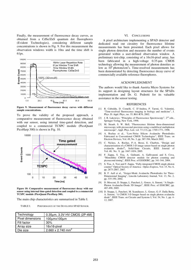
Finally, the measurement of fluorescence decay curves, as
obtained from a CdSe/ZnS quantum dot fluorophores
(Evident Technologies), considering different sample
concentrations is shown in Fig. 9. For this measurement the
observation windows width is 10ns and the time shift is
61ps.
Figure 9: Measurement of fluorescence decay curves with different
sample concentrations.
To prove the validity of the proposed approach, a
comparative measurement of fluorescence decay obtained
with our sensor, using internal time-gated detection, and
coupled to a commercial TCSPC module (PicoQuant
PicoHarp 300) is shown in Fig. 10.
100
1000
10000
0 10 20 30 40 50
Time [ns]
Ev
en
t C
ou
nts
Figure 10: Comparative measurement of fluorescence decay with our
sensor using internal time-gated detection and coupled to a commercial
TCSPC module (PicoQuant PicoHarp 300).
The main chip characteristics are summarized in Table I.
TABLE I. PERFORMANCE OF THE DEVELOPED SPAD SENSOR.
Technology 0.35µm, 3.3V HV CMOS (2P-4M)
Pixel dimensions 100µmx100µm
Fill factor 30%
Array size 16x16-pixel
Die size 2.660 x 2.740 mm2
VI. CONCLUSIONS
A pixel architecture implementing a SPAD detector and dedicated read out circuitry for fluorescence lifetime measurements has been presented. Each pixel allows for single photon detection and measures the number of events generated within a user-defined observation window. A preliminary test-chip, consisting of a 16x16-pixel array, has
been fabricated in a high-voltage 0.35-µm CMOS technology allowing the measurement of photon densities as low as 10
8 photons/cm
2s. Time-resolved measurements has
been demonstrated by detecting fluorescence decay curve of commercially available reference fluorophores.
ACKNOWLEDGMENT
The authors would like to thank Austria Micro Systems for
its support in designing layout structures for the SPADs
implementation and Dr. G. Pedretti for its valuable
assistance in the sensor testing.
REFERENCES
[1] R. Cubeddu, D. Comelli, C. D’Andrea, P. Taroni, G. Valentini, “Time-resolved fluorescence imaging in biology and medicine”, J. Phys. D: Appl. Phys., no. 35, R61-R76, 2002.
[2] J. R. Lakowicz, “Principles of Fluorescence Spectroscopy”, 2nd edn., Springer-Verlag, New York, 1998.
[3] M. Straub, S. W. Hell, “Fluorescence lifetime three-dimensional microscopy with picosecond precision using a multifocal multiphoton microscope”, Appl. Phys. Lett. vol. 73 (13), pp. 1769-1771, 1998.
[4] A. Rochas et al., “Low-Noise Silicon Avalanche Photodiodes Fabricated in Conventional CMOS Technologies”, IEEE Trans. on Electron Devices, Vol. 49, No. 3, pp. 387-394, March 2002.
[5] C. Niclass, A. Rochas, P.-A. Besse, E. Charbon, “Design and characterization of a CMOS 3-D image sensor based on single photon avalanche diodes”, Solid-State Circuits, IEEE Journal of Vol. 40, No. 9, pp. 1847-1854, 2005.
[6] F. Zappa, S. Tisa, A. Gulinatti, A. Gallivanoni and S. Cova, “Monolithic CMOS detector module for photon counting and picosecond timing”, IEEE Proc. of ESSDERC, pp. 341-344, 2004.
[7] S. Tisa, A. Tosi and F. Zappa, “Fully-integrated CMOS single photon counter” Optical Society of America - Optics Express, Vol. 15, No. 6, pp. 2873-2887, 2007.
[8] B. F. Aull et al., "Geiger-Mode Avalanche Photodiodes for Three-Dimensional Imaging", Lincoln Laboratory Journal, Vol. 13, No. 2, pp. 335-350, 2002.
[9] D. Mosconi, D. Stoppa, L. Pancheri, L. Gonzo, A. Simoni, “A Single-Photon Avalanche-Diode 3D Imager”, IEEE Proc. of ESSCIRC, pp. 487-490, 2005.
[10] D. Stoppa, L. Pancheri, M. Scandiuzzo, L. Gonzo, G.-F. Dalla Betta, A. Simoni, “A CMOS 3-D Imager based on single photon avalanche diode”, IEEE Trans. on Circuits and Systems I, Vol. 54, No. 1, pp. 4-12, 2007.
Time gated measurement
TCSPC
253