a 3.3-v 12-b 50-ms/s a/d converter in 0.6-µm cmos with over 80-db sfdr · · 2001-11-30cmos with...
TRANSCRIPT

IEEE JOURNAL OF SOLID-STATE CIRCUITS, VOL. 35, NO. 12, DECEMBER 2000 1769
A 3.3-V 12-b 50-MS/s A/D Converter in 0.6-�mCMOS with over 80-dB SFDR
Hui Pan, Masahiro Segami, Michael Choi, Jing Cao, and Asad A. Abidi, Fellow, IEEE
Abstract—A 12-b analog-to-digital converter (ADC) is opti-mized for spurious-free dynamic range (SFDR) performance atlow supply voltage and suitable for use in modern wireless basestations. The 6–7-b two-stage pipeline ADC uses a bootstrap circuitto linearize the sampling switch of an on-chip sample-and-hold(S/H) and achieves over 80-dB SFDR for signal frequencies up to75 MHz at 50 MSample/s (MSPS) without trimming, calibration,or dithering. INL is 1.3 LSB, differential nonlinearity (DNL) is 0.8LSB. The 6-b and 7-b flash sub-ADCs are implemented efficientlyusing offset averaging and analog folding. In 0.6-m CMOS, the16-mm2 ADC dissipates 850 mW.
Index Terms—A/D converter, analog folding, bootstrap circuit,CMOS analog integrated circuits, IF sampling, spatial filter, spu-rious-free dynamic range.
I. INTRODUCTION
M ODERN wireless base stations digitize the IF band, andseparate individual channels with digital filters [1], [2].
Digitizing at IF poses challenges on the design of the analog-to-digital converter (ADC). First, the spurious-free dynamic range(SFDR) must be over 80 dB so that a weak received channelis not confused with the artifacts arising from digitizing strongchannels. The SFDR of an ADC is defined as [3] the differ-ence in decibels (dB) between the full-scale (FS) fundamentaland the maximum spurious tone in the output spectrum. Thesignal-to-noise ratio (SNR) is relatively less important here, be-cause of the digital processing gain. Second, the conversion ratemust be on the order of 50 Msample/s (MSPS) to accommodatea typical 20-MHz IF band. Third, it is also desirable to main-tain a constant SFDR performance beyond the Nyquist inputfrequency to give more freedom in placing the IF. This requiresan on-chip sample-and-hold (S/H) with good dynamic perfor-mance. So far, only bipolar and BiCMOS ADCs come closeto these specifications [4]–[7], and they all operate from a 5-Vsupply.
This paper presents a 3.3-V 0.6-m 50-MSPS CMOS A/Dconverter demonstrating SFDR greater than 80 dB for inputfrequencies up to 75 MHz without trimming, calibration, ordithering. The fundamental objective is to develop an efficient(compact and low power) and calibration-free ADC architectureoptimized for SFDR. Although 0.6-m CMOS can operate at5 V, part of the research was to anticipate the low voltage needs
Manuscript received April 20, 2000; revised July 15, 2000.H. Pan is with Broadcom Corporation, Irvine, CA 92619 USA (e-mail:
[email protected]).M. Segami is with Yokogawa Electric Corporation, Tokyo, Japan.M. Choi and A. A. Abidi are with the Integrated Circuits and Systems Labo-
ratory, Department of Electrical Engineering, University of California, Los An-geles, CA 90095-1594 USA.
Publisher Item Identifier S 0018-9200(00)10054-X.
of scaled technologies in the future. After a brief introductionto the fundamentals in Section II, a 12-b two-stage pipeline ar-chitecture with a 6–7-b partition is chosen, as described in Sec-tion III. Section IV derives the efficient sub-ADCs. Circuit im-plementation of the major building blocks is described in Sec-tion V. Finally, experimental results are discussed in Section VI,followed by conclusions in Section VII.
II. SFDR: FUNDAMENTALS
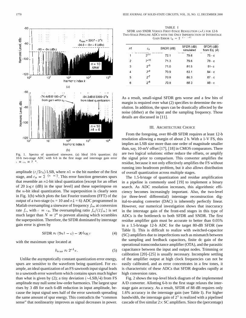
An -bit ideal quantizer exhibits a sawtooth error charac-teristic. With the FS input amplitude normalized to one (FS/2= 1), the periodic error function is parameterized with its fre-quency /LSB = 2 , where the least significant bit(LSB) represents the quantization step. The error distorts anFS input sinewave and creates wideband harmonics, with sig-nificant spectral energy up to the order of. The Fourier se-ries of either the quantized sinewave or the periodic sawtootherror function lead to closed-form expressions for the harmonics[8]–[11] and plots of distortion spectra as shown in Fig. 1(a).The plots for various show that the largest harmonic is locatednear , and is about dB below the fundamental, that is
(1)
and
SFDR (dB) (2)
where is the index of the largest harmonic and the offsetranges from 0 for low resolutions to 6 for high resolutions [10].
Though strict validation of these empirical equations ismathematically interesting, it gives better insight to derive(2) from energy conservation. As increases by one, thequantization error is halved in amplitude, and the total errorenergy LSB/12, which isasymptotically independentof thesignal distribution [12]–[15], decreases by 6 dB. This leads tothe signal-to-noise-and-distortion ratio (SNDR)
SNDR (dB) (3)
Also, now the error sawtooth at double the frequency producestwice as many important harmonics, so the overall spur levelmust go down by an additional 3 dB to keep the total harmonicenergy unchanged, resulting in theterm in (2). This suggeststhat the key to high SFDR should be to spread a given errorenergy across as large a number of spurs as possible.
Imperfections in real ADCs add errors. The linear superposi-tion of those error characteristics on the ideal quantization ap-proximates the overall quantization error to the first order. Forexample, interstage gain errorin a two-stage pipeline ADCcontributes a sawtooth error [16] of frequency , and
0018–9200/00$10.00 © 2000 IEEE
1770 IEEE JOURNAL OF SOLID-STATE CIRCUITS, VOL. 35, NO. 12, DECEMBER 2000
(a)
(b)Fig. 1. Spectra of quantized sinewave. (a) Ideal 10-b quantizer. (b)10-b two-stage ADC with 6-b in the first stage and interstage gain error" = " = 2 .
amplitude LSB, where the bit number of the firststage, and . This error function generates spursthat resemble an -bit ideal quantization [except for an offsetof 20 (dB) in the spur level] and these superimpose onthe -bit ideal quantization. The superposition is clearly seenin Fig. 1(b) which plots the fast Fourier transform (FFT) of theoutput of a two-stage (= 10 and = 6) ADC programmed inMatlab oversampling a sinewave of frequencyat conversionrate , with . The oversampling ratio is setmuch larger than to prevent aliasing which scramblesthe superposition. Therefore, the SFDR dominated by interstagegain error is given by
SFDR (4)
with the maximum spur located at
(5)
Unlike the asymptotically constant quantization error energy,spurs are sensitive to the waveform being quantized. For ex-ample, an ideal quantization of an FS sawtooth input signal leadsto a sawtooth error waveform which contains spurs much higherthan what is given by (2); a tiny deviation LSB ) from FSamplitude may null some low-order harmonics. The largest spurrises by 3 dB for each 6-dB reduction in input amplitude, be-cause the input signal sees half of the error sawtooth spreadingthe same amount of spur energy. This contradicts the “commonsense” that nonlinearity improves as signal decreases in power.
TABLE ISFDRAND SNDR VERSUSFIRST-STAGE RESOLUTION (n1) FOR 12-b
TWO-STAGE PIPELINE ADCS WITH THE ONLY IMPERFECTION OFINTERSTAGE
GAIN ERROR" = 2
As a result, small-signal SFDR gets worse and a few bits ofmargin is required over what (2) specifies to determine the res-olution. In addition, the spurs can be drastically affected by thenoise (dither) at the input and the sampling frequency. Thosedetails are discussed in [11].
III. A RCHITECTURECHOICE
From the foregoing, over 80-dB SFDR requires at least 12-bresolution allowing a margin of about 2 b. With a 1-V FS, thisimplies an LSB size more than one order of magnitude smallerthan, say, 10-mV offset [17], [18] in CMOS comparators. Thereare two logical solutions: either reduce the offsets, or amplifythe signal prior to comparison. This converter amplifies theresidue, because it not only effectively amplifies the FS withoutrunning into headroom problem, but it also allows distributionof overall quantization across multiple stages.
The 1.5-b/stage of quantization and residue amplificationin a pipeline is commonly used [19] to implement a binarysearch. As ADC resolution increases, this algorithmic effi-ciency becomes increasingly important. Also, the two-level(or three-level differential) interstage reconstruction dig-ital-to-analog converter (DAC) is inherently perfectly linear.However, our numerical investigation shows that inaccuracyin the interstage gain of the front-end stages in this type ofADCs is the bottleneck to both SFDR and SNDR. The firstresidue amplifier gain must be accurate to better than 0.05%in a 1.5-b/stage 12-b ADC for the target 80-dB SFDR (seeTable I). This is difficult to realize with switched-capacitor(SC) amplifiers due to imperfections such as mismatch betweenthe sampling and feedback capacitors, finite dc gain of theoperational transconductance amplifier (OTA), and the parasiticcapacitance between the input and output nodes. Trimming orcalibration [20]–[25] is usually necessary. Incomplete settlingof the amplifier output at high clock frequencies can not beeasily calibrated, and as error concentrates in a few tones, itis characteristic of these ADCs that SFDR degrades rapidly athigh conversion rates.
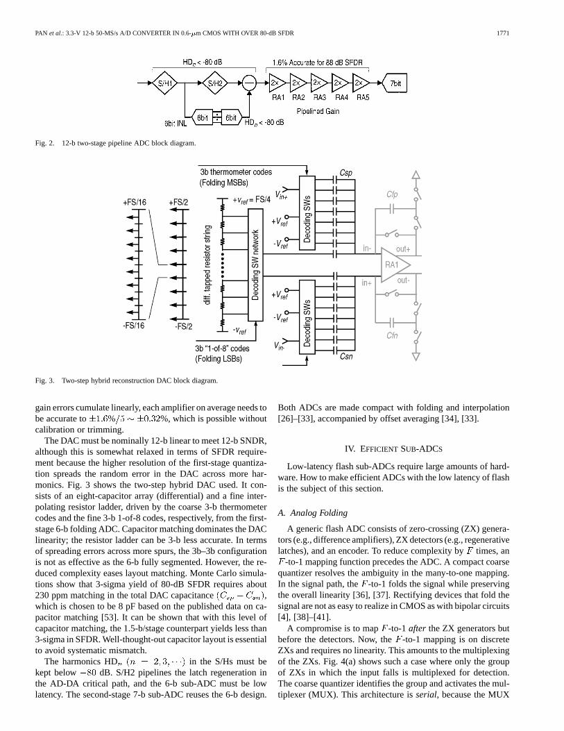
Fig. 2 shows the top-level block diagram of the implementedA/D converter. Allotting 6-b to the first stage relaxes the inter-stage gain accuracy. As a result, SFDR of 88 dB requires only1.6% accuracy in the interstage gain (see Table I). For higherbandwidth, the interstage gain of 2is realized with a pipelinedcascade of five similar 2 SC amplifiers. Since the (percentage)
PAN et al.: 3.3-V 12-b 50-MS/s A/D CONVERTER IN 0.6-m CMOS WITH OVER 80-dB SFDR 1771
Fig. 2. 12-b two-stage pipeline ADC block diagram.
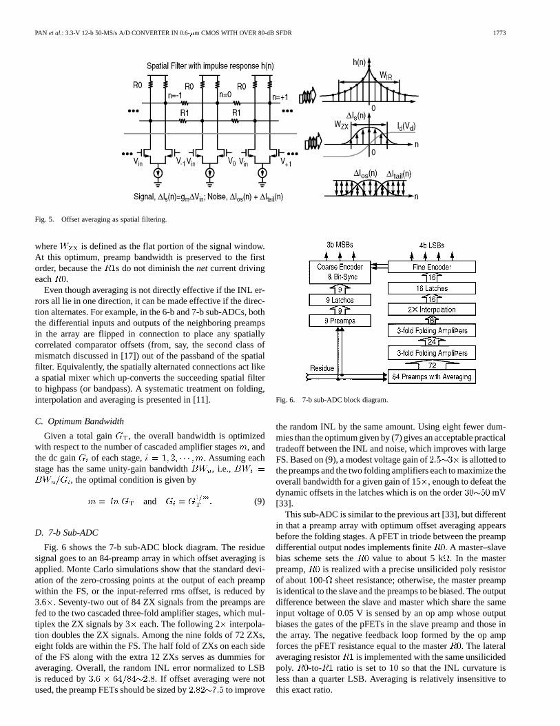
Fig. 3. Two-step hybrid reconstruction DAC block diagram.
gain errors cumulate linearly, each amplifier on average needs tobe accurate to % %, which is possible withoutcalibration or trimming.
The DAC must be nominally 12-b linear to meet 12-b SNDR,although this is somewhat relaxed in terms of SFDR require-ment because the higher resolution of the first-stage quantiza-tion spreads the random error in the DAC across more har-monics. Fig. 3 shows the two-step hybrid DAC used. It con-sists of an eight-capacitor array (differential) and a fine inter-polating resistor ladder, driven by the coarse 3-b thermometercodes and the fine 3-b 1-of-8 codes, respectively, from the first-stage 6-b folding ADC. Capacitor matching dominates the DAClinearity; the resistor ladder can be 3-b less accurate. In termsof spreading errors across more spurs, the 3b–3b configurationis not as effective as the 6-b fully segmented. However, the re-duced complexity eases layout matching. Monte Carlo simula-tions show that 3-sigma yield of 80-dB SFDR requires about230 ppm matching in the total DAC capacitance ,which is chosen to be 8 pF based on the published data on ca-pacitor matching [53]. It can be shown that with this level ofcapacitor matching, the 1.5-b/stage counterpart yields less than3-sigma in SFDR. Well-thought-out capacitor layout is essentialto avoid systematic mismatch.
The harmonics HD in the S/Hs must bekept below dB. S/H2 pipelines the latch regeneration inthe AD-DA critical path, and the 6-b sub-ADC must be lowlatency. The second-stage 7-b sub-ADC reuses the 6-b design.
Both ADCs are made compact with folding and interpolation[26]–[33], accompanied by offset averaging [34], [33].
IV. EFFICIENT SUB-ADCS
Low-latency flash sub-ADCs require large amounts of hard-ware. How to make efficient ADCs with the low latency of flashis the subject of this section.
A. Analog Folding
A generic flash ADC consists of zero-crossing (ZX) genera-tors (e.g., difference amplifiers), ZX detectors (e.g., regenerativelatches), and an encoder. To reduce complexity bytimes, an
-to-1 mapping function precedes the ADC. A compact coarsequantizer resolves the ambiguity in the many-to-one mapping.In the signal path, the -to-1 folds the signal while preservingthe overall linearity [36], [37]. Rectifying devices that fold thesignal are not as easy to realize in CMOS as with bipolar circuits[4], [38]–[41].
A compromise is to map -to-1 after the ZX generators butbefore the detectors. Now, the-to-1 mapping is on discreteZXs and requires no linearity. This amounts to the multiplexingof the ZXs. Fig. 4(a) shows such a case where only the groupof ZXs in which the input falls is multiplexed for detection.The coarse quantizer identifies the group and activates the mul-tiplexer (MUX). This architecture isserial, because the MUX

1772 IEEE JOURNAL OF SOLID-STATE CIRCUITS, VOL. 35, NO. 12, DECEMBER 2000
Fig. 4. Multiplexing of ZXs. (a) Modified flash ADC. (b) SW MUX. (c) Auto MUX. (d) Folding.
waits for the coarse decision. To preserve the flash-like nature,this latency must be removed by automating the MUX.
Fig. 4(b) shows the MUX realized as switches. However, theswitches can be bypassed if the signals from the groups awayfrom the zerocrossing cancel each other. Cancellation happenswhen the ZXs of each adjacent group are reversed in polarity andpeg at the same level [Fig. 4(c)]. The flipped polarity does notchange the result of the fine quantization because the cut point ofthe thermometer codes remains the same. Now, the multiplexeris automatic; the ZXs (characteristics) merge into the foldingcharacteristic [Fig. 4(d)], which is referred to as ZXfolding, todistinguish from the signal folding aforementioned.
The folding is therefore the automatic multiplexing of ZXs,and it realizes amulti-step flashADC [11]. Signals may befolded in many ways. The method described above sums anodd number of ZXs of alternative polarity [30]. The summa-tion can be realized in two steps: subtotal first and then grandtotal, leading to the summation-based cascaded folding [33].This gives the advantage that less parasitics and mismatch intail currents aggregate at the merging node.
Folding multiplies the input signal frequency and the foldingsignal may exceed the bandwidth of the folding circuit. Thisceases to be a problem when a S/H provides a dc-like input tothe folding amplifiers, such as in the sub-ADCs in this pipelinearchitecture.
B. Interpolation and Averaging
Interpolation and averaging lower the number and size of theZX generators [33]. In the commonly used voltage interpola-tion, a resistive voltage divider connects the output of each ad-jacent ZX generator. Often the buffers driving the interpolatingnetwork set the interpolating ZX voltages [30], [31]. With suffi-cient dummies extending the array, the buffers can be removed,because the interfering signals cancel each other and the ZXswithin the FS are not disturbed. Without the buffers, the inter-polation turns into the offset averaging [34].
In this work, offset averaging is optimized based onspatialfiltering. Fig. 5 shows an infinite preamp array with the lateralresistors inserted for offset averaging. The load impedance
of the preamps and the averaging resistorsform a spatialfilter with impulse response [35]
(6)
where the node index . The input differen-tial-pair stages provide the stimuli, with the small-signal cur-rents constituting the signal part. Theoffset currents and the tail current mismatch together approxi-mate white noise. The input referred offset is minimized whenthe impulse response width is equal to the signal window
(i.e., the number of active preamps around zero crossing).This corresponds to amatchedfilter.
For a linear finite array, the boundary condition,,1 must be satisfied to avoid integral nonlin-
earity (INL) curvature at the extremes of input range, whereis the total number of dummy preamps. Conversely, this
condition implies that must be the minimum for agiven INL curvature.
Dummies not only cost extra hardware but also consume pre-cious voltage headroom. The input-referred rms offset normal-ized to LSB is optimum [11] when
(7)
where is the total number of preamps allowed by theavailable headroom. Thus, the overall optimum condition be-comes
(8)
1When the differential outputs at the two ends of a preamp array are cross-coupled through R1 to form a circular array [33], the boundary condition ischanged toW > min(W ;W ).
PAN et al.: 3.3-V 12-b 50-MS/s A/D CONVERTER IN 0.6-m CMOS WITH OVER 80-dB SFDR 1773
Fig. 5. Offset averaging as spatial filtering.
where is defined as the flat portion of the signal window.At this optimum, preamp bandwidth is preserved to the firstorder, because the s do not diminish thenetcurrent drivingeach .
Even though averaging is not directly effective if the INL er-rors all lie in one direction, it can be made effective if the direc-tion alternates. For example, in the 6-b and 7-b sub-ADCs, boththe differential inputs and outputs of the neighboring preampsin the array are flipped in connection to place any spatiallycorrelated comparator offsets (from, say, the second class ofmismatch discussed in [17]) out of the passband of the spatialfilter. Equivalently, the spatially alternated connections act likea spatial mixer which up-converts the succeeding spatial filterto highpass (or bandpass). A systematic treatment on folding,interpolation and averaging is presented in [11].
C. Optimum Bandwidth
Given a total gain , the overall bandwidth is optimizedwith respect to the number of cascaded amplifier stages, andthe dc gain of each stage, . Assuming eachstage has the same unity-gain bandwidth , i.e.,
, the optimal condition is given by
and (9)
D. 7-b Sub-ADC
Fig. 6 shows the 7-b sub-ADC block diagram. The residuesignal goes to an 84-preamp array in which offset averaging isapplied. Monte Carlo simulations show that the standard devi-ation of the zero-crossing points at the output of each preampwithin the FS, or the input-referred rms offset, is reduced by3.6 . Seventy-two out of 84 ZX signals from the preamps arefed to the two cascaded three-fold amplifier stages, which mul-tiplex the ZX signals by 3 each. The following 2 interpola-tion doubles the ZX signals. Among the nine folds of 72 ZXs,eight folds are within the FS. The half fold of ZXs on each sideof the FS along with the extra 12 ZXs serves as dummies foraveraging. Overall, the random INL error normalized to LSBis reduced by . If offset averaging were notused, the preamp FETs should be sized by to improve
Fig. 6. 7-b sub-ADC block diagram.
the random INL by the same amount. Using eight fewer dum-mies than the optimum given by (7) gives an acceptable practicaltradeoff between the INL and noise, which improves with largeFS. Based on (9), a modest voltage gain of is allotted tothe preamps and the two folding amplifiers each to maximize theoverall bandwidth for a given gain of 15, enough to defeat thedynamic offsets in the latches which is on the order mV[33].
This sub-ADC is similar to the previous art [33], but differentin that a preamp array with optimum offset averaging appearsbefore the folding stages. A pFET in triode between the preampdifferential output nodes implements finite . A master–slavebias scheme sets the value to about 5 k . In the masterpreamp, is realized with a precise unsilicided poly resistorof about 100- sheet resistance; otherwise, the master preampis identical to the slave and the preamps to be biased. The outputdifference between the slave and master which share the sameinput voltage of 0.05 V is sensed by an op amp whose outputbiases the gates of the pFETs in the slave preamp and those inthe array. The negative feedback loop formed by the op ampforces the pFET resistance equal to the master. The lateralaveraging resistor is implemented with the same unsilicidedpoly. -to- ratio is set to 10 so that the INL curvature isless than a quarter LSB. Averaging is relatively insensitive tothis exact ratio.
1774 IEEE JOURNAL OF SOLID-STATE CIRCUITS, VOL. 35, NO. 12, DECEMBER 2000
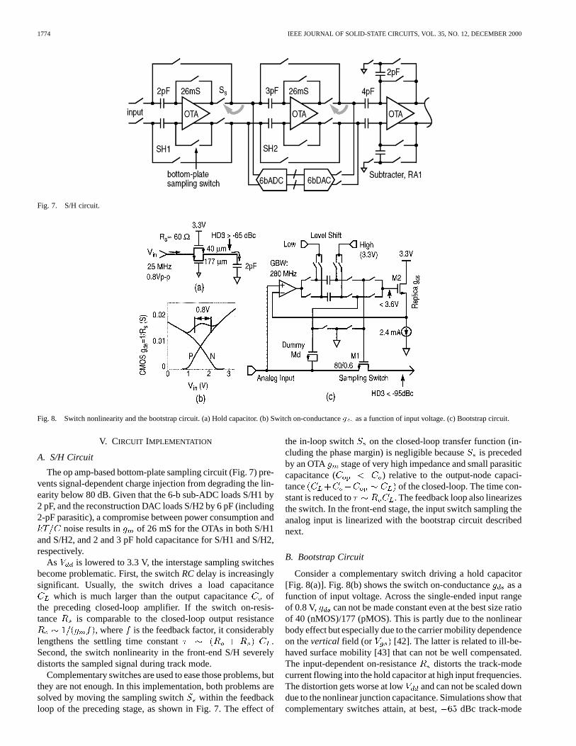
Fig. 7. S/H circuit.
Fig. 8. Switch nonlinearity and the bootstrap circuit. (a) Hold capacitor. (b) Switch on-conductanceg as a function of input voltage. (c) Bootstrap circuit.
V. CIRCUIT IMPLEMENTATION
A. S/H Circuit
The op amp-based bottom-plate sampling circuit (Fig. 7) pre-vents signal-dependent charge injection from degrading the lin-earity below 80 dB. Given that the 6-b sub-ADC loads S/H1 by2 pF, and the reconstruction DAC loads S/H2 by 6 pF (including2-pF parasitic), a compromise between power consumption and
noise results in of 26 mS for the OTAs in both S/H1and S/H2, and 2 and 3 pF hold capacitance for S/H1 and S/H2,respectively.
As is lowered to 3.3 V, the interstage sampling switchesbecome problematic. First, the switchRCdelay is increasinglysignificant. Usually, the switch drives a load capacitance
which is much larger than the output capacitanceofthe preceding closed-loop amplifier. If the switch on-resis-tance is comparable to the closed-loop output resistance
, where is the feedback factor, it considerablylengthens the settling time constant .Second, the switch nonlinearity in the front-end S/H severelydistorts the sampled signal during track mode.
Complementary switches are used to ease those problems, butthey are not enough. In this implementation, both problems aresolved by moving the sampling switch within the feedbackloop of the preceding stage, as shown in Fig. 7. The effect of
the in-loop switch on the closed-loop transfer function (in-cluding the phase margin) is negligible becauseis precededby an OTA stage of very high impedance and small parasiticcapacitance ( ) relative to the output-node capaci-tance of the closed-loop. The time con-stant is reduced to . The feedback loop also linearizesthe switch. In the front-end stage, the input switch sampling theanalog input is linearized with the bootstrap circuit describednext.
B. Bootstrap Circuit
Consider a complementary switch driving a hold capacitor[Fig. 8(a)]. Fig. 8(b) shows the switch on-conductanceas afunction of input voltage. Across the single-ended input rangeof 0.8 V, can not be made constant even at the best size ratioof 40 (nMOS)/177 (pMOS). This is partly due to the nonlinearbody effect but especially due to the carrier mobility dependenceon thevertical field (or [42]. The latter is related to ill-be-haved surface mobility [43] that can not be well compensated.The input-dependent on-resistance distorts the track-modecurrent flowing into the hold capacitor at high input frequencies.The distortion gets worse at low and can not be scaled downdue to the nonlinear junction capacitance. Simulations show thatcomplementary switches attain, at best, dBc track-mode

PAN et al.: 3.3-V 12-b 50-MS/s A/D CONVERTER IN 0.6-m CMOS WITH OVER 80-dB SFDR 1775
Fig. 9. Multiple-V -based OTA design.
distortion for single-ended 0.8-V at the Nyquist input fre-quency of 25 MHz.
To suppress the distortion below the required dB level,a bootstrap circuit is used, as shown in Fig. 8(c). The nMOSsampling switch is turnedON with the gate voltage of areplica FET carrying a constant current of 2.4 mA. The opamp forces the source of to track the analog input. Thisway, the sampling switch copies the of the replica, held con-stant by the fixed bias current. When the sampling switch turnsoff, the dummy switch switches in to balance the loadingof the op amp. At the start of track mode, is switched inbefore the dummy is switched off so that the dummy providescorrelated initial charge to turn on quickly. The prechargedlevel-shift capacitors set the output common-mode voltage ofthe op amp. Simulations show that 280-MHz gain-bandwidthproduct (GBW) of the op amp ensures track-mode distortionlower than dB with maximum gate voltage of 3.6 V. Otherpassive bootstrap schemes [44], [45] dissipate less power butcan not remove the body effect.
C. OTA Design
Some OTA topologies are tailored for implementation at low[45]–[47]. Usually, signal swing is maximized to scale
down the capacitor size. In this case, however, the third-ordernonlinearity in the “linear capacitor” [48] implementing theswitched capacitors limits the swing to 1.6-V peak-to-peakdifferential. Conventional super-cascode topology is suitablefor this swing.
Multiple- -based design, as shown in Fig. 9, maximizesthe available swing. All stacked transistors of the same typeare assigned the same with no margin. Thisrequires a well-thought-out biasing scheme to operate reliablyacross process spreads. Multiple- biases are generated byscaling based on the square law of the MOSFET. The bi-asing and biased transistors when well-matched in layout trackeach other, immune to process and temperature variations.
Since the linear region set by V is less than theinput swing of 1.6-V , the OTA is not free of slewing, whichcauses dynamic nonlinearity or effectively reduces the availablesettling time. As a result, 12-b accuracy is obtained after settlingfor more than 10 the time-constant. The closed-loop band-
width of the S/Hs is 250 MHz, which simulation shows guaran-tees 12-b settling accuracy in half-cycle of 75-MHz clock. Thisgives enough margin for 50-MHz sampling in practice.
DC gain is 80 dB for sufficient margin to obtain the requiredclosed-loop linearity. The auxiliary amplifiers provide about30 gain boost. The GBW must be over 250 MHz so thatthe zero-pole doublet corresponding to the auxiliary amplifierunity-gain frequency is positioned out of the closed-loop band-width to suppress the slow settling component [46]. It shouldnot be too high either; otherwise, the auxiliary amplifier loopmay become unstable. As a result, the final GBW is 300 MHz.The level-shift source followers add a pole to the loop, whichhowever does not destabilize the loop, since it is about threetimes higher than the auxiliary amps GBW. The four auxiliaryamplifiers dissipate a total power comparable to the maincircuit. The OTAs in the first four residue amplifiers use doublecascode topology to take advantage of the reduced residueswing, and this dissipates 50% less power due to absence ofthe auxiliary amplifiers.
Two small input transistors with their drains cross-connectedmaintain the minimum bias necessary to keep the cascode tran-sistorsON at the beginning of each phase when the large inputswing steers all the tail current to one leg. Another option is useof a resistor between the cascode sources [49]. Cutoff of the cas-code transistors is harmful not only because the recovery slowsdown the settling, but also the auxiliary loop becomes unstablesince the drastically reduced of the cascode transistor cannot compensate the auxiliary amplifier.
The OTA output common-mode (CM) voltage is shorted tothe input CM, , in the reset phase, but is raised to
V in the hold phase to maximize output swing.The dual common-mode voltages are realized by two pairs ofswitched level-shift capacitors precharged to two different volt-ages [50].
D. Reconstruction DAC
In Fig. 3, the first (most negative differential) coarse tap,-FS/2, is formed by connecting the top plates (bottom platesin layout) of all the eight-unit capacitors on the positiveside to FS/4 and those on the negative side to
FS ; the second tap corresponds to one of the seven
1776 IEEE JOURNAL OF SOLID-STATE CIRCUITS, VOL. 35, NO. 12, DECEMBER 2000
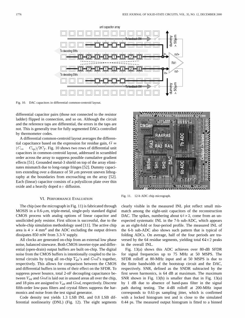
Fig. 10. DAC capacitors in differential common-centroid layout.
differential capacitor pairs (those not connected to the resistorladder) flipped in connection, and so on. Although the circuitand the reference taps are differential, the errors in the taps arenot. This is generally true for fully segmented DACs controlledby thermometer codes.
A differential common-centroid layout averages the differen-tial capacitance based on the expression for residue gain,
. Fig. 10 shows two rows of differential unitcapacitors in common-centroid layout, addressed in scrambledorder across the array to suppress possible cumulative gradienteffects [51]. Grounded metal-3 shield on top of the array elimi-nates mismatch due to long-range fringes [52]. Dummy capaci-tors extending over a distance of 50m prevent uneven lithog-raphy at the boundaries from encroaching on the array [52].Each (linear) capacitor consists of a polysilicon plate over thinoxide and a heavily doped ndiffusion.
VI. PERFORMANCEEVALUATION
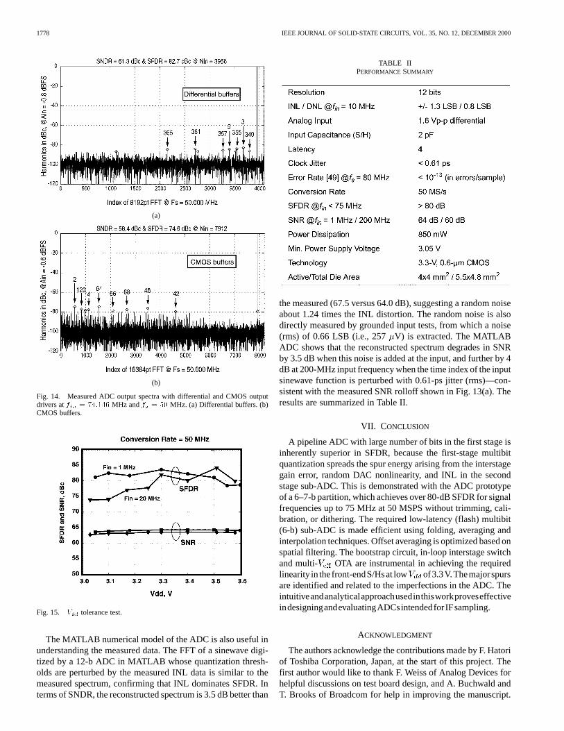
The chip (see the micrograph in Fig. 11) is fabricated throughMOSIS in a 0.6- m, triple-metal, single-poly standard digitalCMOS process with analog options of linear capacitor andunsilicided poly resistor. First silicon is successful, due to thewhole-chip simulation methodology used [11]. The active chiparea is 4 4 mm and the ADC excluding the output driversdissipates 850 mW from 3.3-V supply.
All clocks are generated on-chip from an external low phasenoise, balanced sinewave. Both CMOS inverter-type and differ-ential (open-drain) output buffers are built on-chip. The digitalnoise from the CMOS buffers is intentionally coupled to the in-ternal circuits by tying all on-chip ’s and ’s together,respectively. This allows for comparison between the CMOSand differential buffers in terms of their effect on the SFDR. Tosuppress power bounce, total 2-nF decoupling capacitance be-tween and is laid out in unused areas all over the chip,and 18 pins are assigned to and , respectively. Discretefifth-order low-pass filters and crystal filters suppress the har-monics and noise from the test signal generator.
Code density test yields 1.3 LSB INL and 0.8 LSB dif-ferential nonlinearity (DNL) (Fig. 12). The eight segments
Fig. 11. 12-b ADC chip micrograph.
clearly visible in the measured INL plot reflect small mis-match among the eight-unit capacitors of the reconstructionDAC. The spikes, numbering about , come from an un-expected systematic INL in the 7-b sub-ADC, which appearsas an eight-fold or four-period profile. The measured INL ofthe 6-b sub-ADC also shows such pattern that is typical offolding ADCs. On average, half of the four periods are tra-versed by the 64 residue segments, yielding total peaksin the overall INL.
Fig. 13(a) shows this ADC achieves over 80-dB SFDRfor signal frequencies up to 75 MHz at 50 MSPS. TheSFDR rolloff at 80-MHz input and at 50 MSPS is due tothe finite bandwidth of the bootstrap circuit and the DAC,respectively. SNR, defined as the SNDR subtracted by thefirst seven harmonics, is 64 dB at maximum. The maximumSNR shown in Fig. 13(b) is smaller than that in Fig. 13(a)by 1 dB due to absence of band-pass filter in the signalpath during testing. The 4-dB rolloff at 200-MHz inputcorresponds to 0.61-ps sampling jitter, which is confirmedwith a locked histogram test and is close to the simulated0.44 ps. The measured output histogram is fitted to a binned

PAN et al.: 3.3-V 12-b 50-MS/s A/D CONVERTER IN 0.6-m CMOS WITH OVER 80-dB SFDR 1777
(a)
(b)
Fig. 12. Code density test results. (a) INL atf = 50MS/s, with 16.4 millionsamples. (b) DNL atf = 50 MS/s, with 16.4 million samples.
Gaussian distribution. Jitter is calculated from the best-fitstandard deviation. Perfect fitting can not be achieved unlessthe bin sizes are adjusted with the measured DNL.
The labeled high-order ( ) spurs in Fig. 14(a) arecharacteristic of the INL in the 7-b ADC, based on the followingcalculations. Since the fundamental is dB FS, the inputsinewave sees about 91% of the periods (spikes) in theFS INL plot. From (5), those spikes produce peak harmonics lo-cated around (91% ) . The maximum level ofthose spurs, which is about dB, is close to what (4) predictsfor the case of and , which approximatesthe measured INL profile.
Using CMOS inverter-type output buffers, the measuredSNR and SFDR remain unchanged at low input frequencies,but decay faster as the input increases in frequency. The rolloffcorresponds to about 1.8-ps sampling jitter. This indicates thatthe bounce from the CMOS output drivers is picked up by theinverter-type clock buffers but rejected by other differentialcircuits. Fig. 14(b) shows how the output spectrum is affected.The dominant even-order harmonics confirm the single-endednoise coupling. The bounce brings down the SNR by 2.9 dB(from 61.3 to 58.4 dB), but still not enough to apparently spreadout the high-order spurs. This makes sense because dithering is
(a)
(b)
Fig. 13. Dynamic performance.
not effective until the noise reaches a level comparable to theperiod of the INL pattern responsible for the high-order spurs.In this case, the period is about 7-b LSB, which correspondsto about 42 dB SNR.
The largest spur is among the second to the fifth harmonics,which tend to fluctuate by up to 3 dB between measurements.The fluctuation can be ascribed to the finite FFT points andnoise [54], but more likely in this case to the sensitivity to vari-ation in input amplitude and offset, typical of the low-order har-monics arising from quantization [11]. If it were not for the DACnonlinearity, the largest spur should be among the high orders( ). Since the largest spur actually appears at low-orderand is only a few decibels higher, the DAC must contributelow-order harmonics comparable to those from the 7-b INL.Even though the high-order spurs limit small-signal SFDR be-cause they increase by 0.5 dB for each decibel reduction in inputamplitude, they can be removed by correcting the 7-b systematicINL error. In contrast, the DAC errors arising from random ca-pacitor mismatch presents a fundamental limitation to the SFDRunless they are dynamically scrambled [55]–[60]. Distortion inthe S/Hs produces a dominant third-order harmonic, which doesnot appear until the input frequency goes beyond 75 MHz.
Fig. 15 shows that the ADC works to 3.05-V supply.
1778 IEEE JOURNAL OF SOLID-STATE CIRCUITS, VOL. 35, NO. 12, DECEMBER 2000
(a)
(b)
Fig. 14. Measured ADC output spectra with differential and CMOS outputdrivers atf = 74:146 MHz andf = 50 MHz. (a) Differential buffers. (b)CMOS buffers.
Fig. 15. V tolerance test.
The MATLAB numerical model of the ADC is also useful inunderstanding the measured data. The FFT of a sinewave digi-tized by a 12-b ADC in MATLAB whose quantization thresh-olds are perturbed by the measured INL data is similar to themeasured spectrum, confirming that INL dominates SFDR. Interms of SNDR, the reconstructed spectrum is 3.5 dB better than
TABLE IIPERFORMANCESUMMARY
the measured (67.5 versus 64.0 dB), suggesting a random noiseabout 1.24 times the INL distortion. The random noise is alsodirectly measured by grounded input tests, from which a noise(rms) of 0.66 LSB (i.e., 257 V) is extracted. The MATLABADC shows that the reconstructed spectrum degrades in SNRby 3.5 dB when this noise is added at the input, and further by 4dB at 200-MHz input frequency when the time index of the inputsinewave function is perturbed with 0.61-ps jitter (rms)—con-sistent with the measured SNR rolloff shown in Fig. 13(a). Theresults are summarized in Table II.
VII. CONCLUSION
A pipeline ADC with large number of bits in the first stage isinherently superior in SFDR, because the first-stage multibitquantization spreads the spur energy arising from the interstagegain error, random DAC nonlinearity, and INL in the secondstage sub-ADC. This is demonstrated with the ADC prototypeof a 6–7-b partition, which achieves over 80-dB SFDR for signalfrequencies up to 75 MHz at 50 MSPS without trimming, cali-bration, or dithering. The required low-latency (flash) multibit(6-b) sub-ADC is made efficient using folding, averaging andinterpolation techniques. Offset averaging is optimized based onspatial filtering. The bootstrap circuit, in-loop interstage switchand multi- OTA are instrumental in achieving the requiredlinearity in the front-endS/Hsat low of3.3V.Themajorspursare identified and related to the imperfections in the ADC. TheintuitiveandanalyticalapproachusedinthisworkproveseffectiveindesigningandevaluatingADCsintendedfor IFsampling.
ACKNOWLEDGMENT
The authors acknowledge the contributions made by F. Hatoriof Toshiba Corporation, Japan, at the start of this project. Thefirst author would like to thank F. Weiss of Analog Devices forhelpful discussions on test board design, and A. Buchwald andT. Brooks of Broadcom for help in improving the manuscript.

PAN et al.: 3.3-V 12-b 50-MS/s A/D CONVERTER IN 0.6-m CMOS WITH OVER 80-dB SFDR 1779
T. Brooks suggested the in-loop switch action as presented inSection V-A.
REFERENCES
[1] T. Gratzek, B. Brannon, J. Camp, and F. Murden, “A new paradigmfor base station receivers: High IF sampling + digital filtering,” in1997 IEEE Radio Frequency Integrated Circuits Symp., June 1997, pp.143–146.
[2] , “ADCs for digital receivers: The whole world tunes in,” in1996IEEE MTT-S Dig., pp. 1335–1338.
[3] D. B. Chester, D. H. Damerow, and C. Olmstead, “Analog to digitalconverter requirements and implementations for narrowband channel-ization applications,” inIEEE Int. Conf. Acoustics, Speech and SignalProcessing, vol. 4, Mar. 1992, pp. 325–328.
[4] F. Murden and R. Gosser, “12-b 50-Msample/s two-stage A/D con-verter,” in ISSCC Dig. Tech. Papers, San Francisco, CA, Feb. 1995, pp.278–279.
[5] Analog Devices, AD9042 Data Sheet, 1996.[6] P. Vorenkamp and R. Roovers, “A 12-b 60-MSample/s cascaded folding
and interpolating ADC,”IEEE J. Solid-State Circuits, vol. 32, pp.1876–1886, Dec. 1997.
[7] D. Birdsall and A. Kuckreja, “A 12-bit, 65 MSPS BiCMOS ADC forcellular base-station applications,” inProc. 1998 Bipolar/BiCMOS Cir-cuits and Technology Meeting, Sept. 1998, pp. 43–46.
[8] A. G. Clavier, P. F. Panter, and D. D. Grieg, “Distortion in a pulse countmodulation system,”AIEE Trans., vol. 66, pp. 989–1005, 1947.
[9] D. R. Martin and D. J. Secor, “High-speed analog-to-digital converters incommunication systems: Terminology, architecture, theory and perfor-mance,” TRW Electronics Systems Group, Redondo Beach, CA, Nov.1981.
[10] W. T. Colleran, “A 10-bit 100-MS/s A/D converter using folding, in-terpolating, and analog encoding,” Ph.D. dissertation, Univ. California,Los Angeles, CA, Dec. 1993.
[11] H. Pan, “A 3.3-V 12-b 50-MS/s A/D converter in 0.6-�m CMOS withover 80-dB SFDR,” Ph.D. dissertation, UCLA, Dec. 1999.
[12] W. R. Bennett, “Spectra of quantized signals,”Bell Syst. Tech. J., vol.27, pp. 446–472, July 1948.
[13] A. Gersho, “Principle of quantization,”IEEE Trans. Circuits Syst., vol.CAS-25, pp. 427–436, July 1978.
[14] R. M. Gray, “Quantization noise spectra,”IEEE Trans. Inform. Theory,vol. 36, pp. 1220–1244, Nov. 1990.
[15] R. M. Gray and D. L. Neuhoff, “Quantization,”IEEE Trans. Inform.Theory, vol. 44, pp. 1–63, Oct. 1998.
[16] S. H. Lewis and P. R. Gray, “A pipelined 5-Msample/s 9-bit analog-to-digital converter,”IEEE J. Solid-State Circuits, vol. 22, pp. 954–961,Dec. 1987.
[17] M. J. M. Pelgrom, A. C. J. Duinmaijer, and A. P. G. Welbers, “Matchingproperties of MOS transistors,”IEEE J. Solid-State Circuits, vol. 24, pp.1433–1440, Oct. 1989.
[18] M. J. M. Pelgrom and M. Vertregt, “CMOS technology for mixed signalICs,” Solid-State Electron., vol. 41, pp. 967–974, July 1997.
[19] S. H. Lewiset al., “A 20-b 20-Msample/s analog-to-digital converter,”IEEE J. Solid-State Circuits, vol. 27, pp. 351–358, Mar. 1992.
[20] H.-S. Lee, D. A. Hodges, and P. R. Gray, “A self-calibrating 12-b CMOSA/D converter,”IEEE J. Solid-State Circuits, vol. SC-19, pp. 813–819,Dec. 1984.
[21] Y. M. Lin, B. Kim, and P. R. Gray, “A 13-b 2.5-MHz self-calibratedpipelined A/D converter in 3-�m CMOS,” IEEE J. Solid-State Circuits,vol. 26, pp. 628–636, Dec. 1991.
[22] S.-H. Lee and B.-S. Song, “Digital-domain calibration of multistepanalog-to-digital converters,”IEEE J. Solid-State Circuits, vol. 27, pp.1679–1688, Dec. 1992.
[23] M. de Wit, K.-S. Tan, and R. K. Hester, “A low-power 12-b analog-to-digital converter with on-chip precision trimming,”IEEE J. Solid-StateCircuits, vol. 28, pp. 455–461, Dec. 1993.
[24] E. G. Soenen and R. L. Geiger, “An architecture and an algorithm forfully digital correction of monolithic pipelined ADCs,”IEEE Trans. Cir-cuits Syst. II, vol. 42, pp. 143–153, Dec. 1995.
[25] I. E. Opris, L. D. Lewicki, and B. C. Wong, “A single-ended 12-bit 10Msample/s self-calibrating piepline A/D converter,”IEEE J. Solid-StateCircuits, vol. 33, pp. 1898–1903, Dec. 1998.
[26] R. E. J. van de Grift, I. W. J. M. Rutten, and M. van der Veen, “An 8-bitvideo ADC incorporating folding and interpolation techniques,”IEEEJ. Solid-State Circuits, vol. SC-22, pp. 944–953, Dec. 1987.
[27] R. J. van de Plassche and P. Baltus, “An 8-bit 100-MHz full-Nyquistanalog-to-digital converter,”IEEE J. Solid-State Circuits, vol. 23, pp.1334–1344, Dec. 1988.
[28] W. T. Colleran and A. A. Abidi, “A 10-b 75-MHz two-stage pipelinedbipolar A/D converter,” IEEE J. Solid-State Circuits, vol. 28, pp.1187–1199, Dec. 1993.
[29] R. Roovers and M. Steyaert, “Design of CMOS A/D converters withfolding and/or interpolating techniques,” inAdvanced A-D and D-AConversion Techniques and Their Applications, July 6–8, 1994, pp.76–81.
[30] B. Nauta and A. G. W. Venes, “A 70-MS/s 110-mW 8-b CMOS foldingand interpolating A/D converter,”IEEE J. Solid-State Circuits, vol. 32,pp. 1302–1308, Dec. 1995.
[31] A. G. W. Venes and R. J. van de Plassche, “An 80-MHz, 80-mW, 8-bCMOS folding A/D converter with distributed track-and-hold prepro-cessing,”IEEE J. Solid-State Circuits, vol. 31, pp. 1846–1853, Dec.1996.
[32] M. Flynn and B. Sheahan, “A 400MSample/s 6-b CMOS folding andinterpolating ADC,” inISSCC Dig. Tech. Papers, San Francisco, CA,Feb. 1998, pp. 150–151.
[33] K. Bult and A. Buchwald, “An embedded 240-mW 10-b 50MS/S CMOSADC in 1-mm ,” IEEE J. Solid-State Circuits, vol. 32, pp. 1887–1895,Dec. 1997.
[34] K. Kattmann and J. Barrow, “A technique for reducing differential non-linearity errors in flash A/D converters,” inISSCC Dig. Tech. Papers,San Francisco, CA, Feb. 1991, pp. 170–171.
[35] J. L. White and A. A. Abidi, “Active resistor networks as 2D sampleddata filters,”IEEE Trans. Circuits Syst. I: Fundamental Theory and Ap-plications, vol. 39, pp. 724–733, Sept. 1992.
[36] B. D. Smith, “An unusual analog-digital conversion method,”IRE Trans.Instrum. Meas., pp. 155–160, June 1956.
[37] J. D. Edson and H. H. Henning, “Broadband codecs for an experimental224 Mb/s PCM terminal,”Bell Syst. Tech. J., pp. 1887–1940, Nov. 1965.
[38] A. Arbel and R. Kurz, “Fast ADC,”IEEE Trans. Nucl. Sci., vol. NS-22,pp. 446–451, Feb. 1975.
[39] U. Fieldler and D. Seitzer, “A high-speed 8-bit A/D converter based ona gray-code multiple folding circuit,”IEEE J. Solid-State Circuits, vol.SC-14, pp. 547–551, June 1979.
[40] R. J. van de Plassche and R. E. J. van de Grift, “A high-speed 7 bit A/Dconverter,”IEEE J. Solid-State Circuits, vol. SC-14, pp. 938–943, Dec.1979.
[41] R. E. J. van de Grift and R. J. van de Plassche, “A monolithic 8-bit videoA/D converter,”IEEE J. Solid-State Circuits, vol. SC-19, pp. 374–378,June 1984.
[42] T. Ando, A. B. Fowler, and F. Stern, “Electronic properties of two-di-mensional systems,”Rev. Mod. Phys., vol. 54, pp. 437–672, 1982.
[43] G. S. Gildenblat and C.-L. Huang, “Engineering model of inversionchannel mobility for 60–300 K temperature range,”Electron. Lett., vol.25, pp. 634–636, May 1989.
[44] M. de Wit, “Sample and hold circuitry and methods,” U.S. Patent5170075, Texas Instruments Inc., Dec. 8, 1992.
[45] A. M. Abo and P. R. Gray, “A 1.5-V 10-bit 14.3-MS/s CMOS pipelineanalog-to-digital converter,”IEEE J. Solid-State Circuits, vol. 34, pp.599–606, May 1999.
[46] K. Bult and G. J. G. M. Geelen, “A fast-settling CMOS op amp for SCcircuits with 90-dB dc gain,”IEEE J. Solid-State Circuits, vol. 25, pp.1379–1384, Dec. 1990.
[47] T. B. Cho and P. R. Gray, “A 10-b 20-Msample/s 35-mW pipeline A/Dconverter,” IEEE J. Solid-State Circuits, vol. 30, pp. 166–172, Mar.1995.
[48] T.-I. Liou and C.-S. Teng, “n-poly-to-n -silicon capacitor structuresfor single-poly analog CMOS and BiCMOS processes,”IEEE Trans.Electron Dev., vol. 36, pp. 1620–1628, Sept. 1989.
[49] C. W. Mangelsdorf, “A 400-MHz input flash converter with error cor-rection,” IEEE J. Solid-State Circuits, vol. 25, pp. 184–191, Feb. 1990.
[50] K. Y. Kim, N. Kusayanagi, and A. A. Abidi, “A 10-b 100-MS/s CMOSA/D converter,”IEEE J. Solid-State Circuits, vol. 32, pp. 302–311, Mar.1997.
[51] C. S. G. Conroy, W. A. Lane, and M. A. Moran, “Statistical design tech-niques for D/A converters,”IEEE J. Solid-State Circuits, vol. 24, pp.1118–1128, Aug. 1989.
[52] M. J. McNutt, S. LeMarquis, and J. L. Dunkley, “Systematic capacitancematching errors and corrective layout procedures,”IEEE J. Solid-StateCircuits, vol. 29, pp. 611–616, May 1994.
[53] H. P. Tuinhout, H. Elzinga, J. T. Brugman, and F. Postma, “Thefloating gate measurement technique for characterization of capacitormatching,” IEEE Trans. Semicond. Manufact., vol. 9, pp. 2–8, Feb.1996.
[54] P. Carbone and D. Petri, “Effective frequency-domain ADC testing,”IEEE Trans. Circuits Syst. II, vol. 47, pp. 660–663, July 2000.
1780 IEEE JOURNAL OF SOLID-STATE CIRCUITS, VOL. 35, NO. 12, DECEMBER 2000
[55] L. R. Carley, “A noise shaping coder topology for 15+-bit converters,”IEEE J. Solid-State Circuits, vol. 24, pp. 267–273, Apr. 1989.
[56] B. H. Leung and S. Sutarja, “Multibit D S A/D converter incorporatinga novel class of dynamic element matching techniques,”IEEE Trans.Circuits Syst. II, vol. 39, pp. 35–51, Jan. 1992.
[57] R. T. Baird and T. S. Fiez, “Linearity enhancement of multibit�� A/Dand D/A converters using data-weighted averaging,”IEEE Trans. Cir-cuits Syst. II, vol. 42, pp. 753–762, Dec. 1995.
[58] R. Radke, A. Eshraghi, and T. S. Fiez, “A spurious-free delta–sigmaDAC using rotated data weighted averaging,” inProc. IEEE 1999Custom Integrated Circuits Conf., May 1999, pp. 125–128.
[59] R. Adams, K. Q. Nguyen, and K. Sweetland, “A 113-dB SNR oversam-pling DAC with segmented noise-shaped scrambling,”IEEE J. Solid-State Circuits, vol. 33, pp. 1871–1878, Dec. 1998.
[60] I. Galton, “Digital cancellation of D/A converter noise in pipelined A/Dconverters,” IEEE Trans. Circuits Syst. II, to be published.
Hui Pan received the B.E. degree in electrical engi-neering and the M.S. degree in applied physics fromTsinghua University, Beijing, China, in 1983 and1986, respectively, and the Ph.D. degree in electricalengineering from the University of California, LosAngeles, in 1999.
From 1986 to 1991, he was with the Departmentof Physics, Tsinghua University, as a Lecturer. In1992, he joined the Photonics Research Laboratory,State University of New York, Buffalo, where hestudied organic compounds and polymers promising
for broadband communications. He is currently a Staff Scientist at BroadcomCorporation, Irvine, CA. His research interests are in design of integratedcircuits and systems for wireless and wireline communications.
Masahiro Segamiwas born in Gifu, Japan, on April12, 1963. He received the B.E. and M.E. degreesin electrical engineering from the Tokyo Instituteof Technology, Tokyo, Japan, in 1986 and 1988,respectively.
In 1988, he joined the Research and DevelopmentDepartment, Yokogawa Electric Corporation, Tokyo,where he has been engaged in the developmentof high-speed A/D converters for measuring in-struments. His research interest is in the area oflow-power and high-speed mixed-signal IC design.
Mr. Segami is a member of the Institute of Electrical Engineers of Japan.
Michael Choi was born in Seoul, Korea, in 1971.He received the B.S.E.E. degree from the Universityof California, Irvine, in 1994, and the M.S.E.E. de-gree from the University of California, Los Angeles(UCLA), in 1998. He is currently working toward thePh. D. degree in electrical engineering at UCLA.
His research interests include the design ofanalog, mixed-signal, and data-conversion integratedcircuits.
Jing Caowas born in Shanxi, China, in 1971. He re-ceived the B.S. degree in microelectronics and theM.S. degree in semiconductor physics from PekingUniversity, Beijing, China, in 1990 and 1995, respec-tively, and the M.S. degree in eletrical engineeringfrom the University of California, Los Angeles, in1999.
He is currently with Conexant Systems, Inc., New-port Beach, CA. His research interests include analogand mixed-signal circuit design.
Asad A. Abidi (S’75–M’80–SM’95–F’96) receivedthe B.Sc. (Hons.) degree from Imperial College,London, U.K., in 1976 and the M.S. and Ph.D.degrees in electrical engineering from the Universityof California, Berkeley, in 1978 and 1981.
He was at Bell Laboratories, Murray Hill, NJ,from 1981 to 1984 as a Member of Technical Staff inthe Advanced LSI Development Laboratory. Since1985, he has been with the Electrical EngineeringDepartment, University of California, Los Angeles,where he is a Professor. He was a Visiting Faculty
Researcher at Hewlett Packard Laboratories during 1989. His research interestsare in CMOS RF design, high-speed analog integrated circuit design, dataconversion, and other techniques of analog signal processing. He was theProgram Secretary for the International Solid-State Circuits Conference from1984 to 1990 and General Chairman of the Symp. on VLSI Circuits in 1992.He was Secretary of the IEEE Solid-State Circuits Council from 1990 to 1991.From 1992 to 1995, he was Editor of the IEEE JOURNAL OF SOLID-STATE
CIRCUITS.Dr. Abidi has received the 1988 TRW Award for Innovative Teaching and
the 1997 IEEE Donald G. Fink Award. He was a corecipient of the Best PaperAward at the 1995 European Solid-State Circuits Conference, the Jack KilbyBest Student Paper Award at the 1996 International Solid-State Circuits Con-ference (ISSCC), the Jack Raper Award for Outstanding Technology DirectionsPaper at the 1997 ISSCC, and the Design Contest Award at the 1998 DesignAutomation Conference.