9 maximize the run time in automotive 50 maximize the run ... · a look at the new ansi/esda/jedec...
TRANSCRIPT

Visit analogdialogue.com
Choosing the Most Suitable MEMS Accelerometer for Your Application—Part 1
A Look at the New ANSI/ESDA/JEDEC JS-002 CDM Test Standard
High Precision Voltage Source
How to Choose Cool Running, High Power, Scalable POL Regulators and Save Board Space
Choosing the Most Suitable MEMS Accelerometer for Your Application—Part 2
Pin-Compatible, High Input Impedance ADC Family Enables Ease of Drive and Broadens ADC Driver Selection
Strategies for Choosing the Appropriate Microcontroller when Developing Ultra Low Power Systems
Radically Extending Bandwidth to Crush the X-Band Frequencies Using a Track-and-Hold Sampling Amplifier and RF ADC
1
2
3
4
5
6
7
8
9 Maximize the Run Time in Automotive Battery Stacks Even as Cells Age
Volume 51, Number 4, 2017 Your Engineering Resource for Innovative Design
Visit analogdialogue.com
Choosing the Most Suitable MEMS Accelerometer for Your Application—Part 1
A Look at the New ANSI/ESDA/JEDEC JS-002 CDM Test Standard
High Precision Voltage Source
How to Choose Cool Running, High Power, Scalable POL Regulators and Save Board Space
Choosing the Most Suitable MEMS Accelerometer for Your Application—Part 2
Pin-Compatible, High Input Impedance ADC Family Enables Ease of Drive and Broadens ADC Driver Selection
Strategies for Choosing the Appropriate Microcontroller when Developing Ultra Low Power Systems
Radically Extending Bandwidth to Crush the X-Band Frequencies Using a Track-and-Hold Sampling Amplifier and RF ADC
5
11
16
22
28
34
41
45
50 Maximize the Run Time in Automotive Battery Stacks Even as Cells Age
Volume 51, Number 4, 2017 Your Engineering Resource for Innovative Design
Analog Dialogue Volume 51 Number 42
In This Issue
Choosing the Most Suitable MEMS Accelerometer for Your Application—Part 1There are hundreds of accelerometers to choose from to measure acceleration, tilt, and vibration or shock. Chris Murphy, a senior applications engineer, can help you find your way through the jungle of options in this article, “Choosing the Most Suitable MEMS Accelerometer for Your Application—Part 1.”
5
A Look at the New ANSI/ESDA/JEDEC JS-002 CDM Test Standard It is well known that the biggest cause, by far, of ESD damage to an IC during device handling in a manufacturing environment is from charged device events. This standard has the opportunity to be the first true industry-wide CDM test standard. Many companies, including Analog Devices, have transitioned to testing using JS-002 for all new products. Take a closer look at it in this article.
11
High Precision Voltage SourceAuthor Michael Lynch discusses combining an ultrastable reference with a 20-bit, 1 ppm DAC and buffering the output with an ultralow offset, drift, rail-to-rail amplifier. By doing so, you will get a reference voltage source that achieves 1 ppm resolution with 1 ppm INL, and better than 1 ppm FSR long-term drift.
16
Rarely Asked Questions—Issue 146: Why Is My Processor Leaking Power? That Sounds Like an Open-Ended QuestionBringing you the answer to this RAQ is Abhinay Patil, a staff field application manager in Bangalore. Could it be a poorly driven CMOS input gate driver? Abhinay knows for sure.
19
How to Choose Cool Running, High Power, Scalable POL Regulators and Save Board SpaceAfshin’s article concentrates on point-of-load (POL) regulators. Do you need more current than 40 A or 160 A? Just add another regulator in parallel. What about the heat and efficiency? Find out in this article.
22
Analog Dialogue Volume 51 Number 4 3
Choosing the Most Suitable MEMS Accelerometer for Your Application—Part 2We’re happy to present part 2 of this article. We hope these two articles help you to find the right MEMS devices for your acceleration, tilt, and vibration or shock measurement applications.
28
Pin-Compatible, High Input Impedance ADC Family Enables Ease of Drive and Broadens ADC Driver SelectionMaithil Pachchigar introduces you to the 16-/18-/20-bit AD4000 family in this article. System designers are often forced to select a high power, high speed amplifier to drive the switched capacitor SAR ADC. Maithil’s article also addresses this common pain point.
34
Rarely Asked Questions—Issue 147: Synchronous Rectification on the Secondary SideWould it make sense to replace Schottky diodes in an isolated, synchronous rectifier application with MOSFETs? Frederik Dostal has the answer in this RAQ.
39
Strategies for Choosing the Appropriate Microcontroller when Developing Ultra Low Power SystemsDo you have a challenging ultra low power design? Our M3 and M4 controllers could help. Monica Redon’s feature article offers some insight on choosing the right microcontroller for your ultra low power system.
41
Radically Extending Bandwidth to Crush the X-Band Frequencies Using a Track-and-Hold Sampling Amplifier and RF ADCUsing a track-and-hold sampling amplifier (THA) in the signal chain can extend the bandwidth well beyond the ADCs sample bandwidth. Rob Reeder, our senior application engineer, introduces you to this idea in his article about extending bandwidth.
45

Analog Dialogue Volume 51 Number 44
In This Issue
Maximize the Run Time in Automotive Battery Stacks Even as Cells AgeA common issue when loading batteries is mismatched cells. Cells will age and mismatch with repeated use. This article by Samuel Nork and Tony Armstrong introduces you to an active balancing battery loading technique to recover battery capacity in the pack.
50
Rarely Asked Questions—Issue 147: Unique Gate Drive Applications Enable Rapidly Switching On/Off for Your High Power AmplifierA special design tip is offered by Peter Delos and Jarrett Liner. Originally designed for pulsed radar applications, this circuit could be used wherever you must switch an RF source on/off within 200 ns.
54
Analog Dialogue is a technical magazine created and
published by Analog Devices. It provides in-depth design
related information on products, applications, technology,
software, and system solutions for analog, digital, and
mixed-signal processing. Published continuously for
50 years—starting in 1967—it is produced as a monthly
online edition and as a printable quarterly journal featuring
article collections. For history buffs, the Analog Dialogue
archive includes all issues, starting with Volume 1, Number 1,
and four special anniversary editions. To access articles,
the archive, the journal, design resources, and to subscribe,
visit the Analog Dialogue homepage, analogdialogue.com.
Bernhard Siegel, Editor Bernhard became editor of Analog Dialogue in March 2017, when the preceding editor, Jim Surber, decided to retire. Bernhard has been with Analog Devices for over 25 years, starting at the ADI
Munich office in Germany.
Bernhard has worked in various engineering roles including sales, field applications, and product engineering, as well as in technical support and marketing roles.
Residing near Munich, Germany, Bernhard enjoys spending time with his family and playing trombone and euphonium in both a brass band and a symphony orchestra.
You can reach him at [email protected].
Analog Dialogue Volume 51 Number 4 5
Share on
Table 1. Accelerometer Grade and Typical Application Area
Accelerometer Grade
Main Application Bandwidth g-Range
ConsumerMotion, static acceleration
0 Hz 1 g
Automotive Crash/stability 100 Hz <200 g/2 g
IndustrialPlatform
stability/tilt5 Hz to 500 Hz 25 g
TacticalWeapons/craft
navigation<1 kHz 8 g
NavigationSubmarine/craft
navigation>300 Hz 15 g
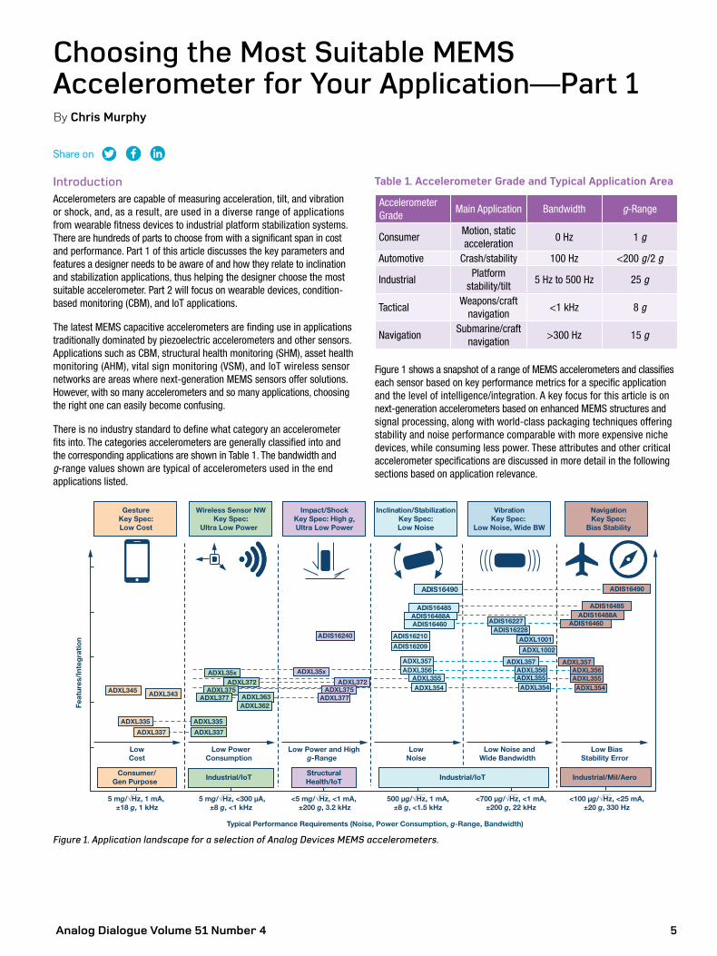
Figure 1 shows a snapshot of a range of MEMS accelerometers and classifies each sensor based on key performance metrics for a specific application and the level of intelligence/integration. A key focus for this article is on next-generation accelerometers based on enhanced MEMS structures and signal processing, along with world-class packaging techniques offering stability and noise performance comparable with more expensive niche devices, while consuming less power. These attributes and other critical accelerometer specifications are discussed in more detail in the following sections based on application relevance.
IntroductionAccelerometers are capable of measuring acceleration, tilt, and vibration or shock, and, as a result, are used in a diverse range of applications from wearable fitness devices to industrial platform stabilization systems. There are hundreds of parts to choose from with a significant span in cost and performance. Part 1 of this article discusses the key parameters and features a designer needs to be aware of and how they relate to inclination and stabilization applications, thus helping the designer choose the most suitable accelerometer. Part 2 will focus on wearable devices, condition-based monitoring (CBM), and IoT applications.
The latest MEMS capacitive accelerometers are finding use in applications traditionally dominated by piezoelectric accelerometers and other sensors. Applications such as CBM, structural health monitoring (SHM), asset health monitoring (AHM), vital sign monitoring (VSM), and IoT wireless sensor networks are areas where next-generation MEMS sensors offer solutions. However, with so many accelerometers and so many applications, choosing the right one can easily become confusing.
There is no industry standard to define what category an accelerometer fits into. The categories accelerometers are generally classified into and the corresponding applications are shown in Table 1. The bandwidth and g-range values shown are typical of accelerometers used in the end applications listed.
Choosing the Most Suitable MEMS Accelerometer for Your Application—Part 1 By Chris Murphy
Figure 1. Application landscape for a selection of Analog Devices MEMS accelerometers.
Typical Performance Requirements (Noise, Power Consumption, g-Range, Bandwidth)
5 mg/√Hz, 1 mA, ±18 g, 1 kHz
<5 mg/√Hz, <1 mA, ±200 g, 3.2 kHz
500 µg/√Hz, 1 mA,±8 g, <1.5 kHz
<700 µg/√Hz, <1 mA,±200 g, 22 kHz
<100 µg/√Hz, <25 mA,±20 g, 330 Hz
5 mg/√Hz, <300 µA,±8 g, <1 kHz
GestureKey Spec:Low Cost
Impact/ShockKey Spec: High g,Ultra Low Power
Inclination/StabilizationKey Spec:Low Noise
VibrationKey Spec:
Low Noise, Wide BW
NavigationKey Spec:
Bias Stability
Wireless Sensor NWKey Spec:
Ultra Low Power
Industrial/IoT Industrial/IoT
ADXL363
Consumer/Gen Purpose
ADXL372
ADIS16228ADXL1001
ADIS16209
ADIS16210
ADXL343
ADXL372ADXL354ADXL345
ADXL362
ADXL356ADXL357 ADXL357
ADIS16240
Feat
ures
/Int
egra
tio
n
ADXL1002
ADXL375ADXL377
ADXL356
ADXL354ADXL355
ADXL337
ADXL335
ADXL337
ADIS16488A
ADIS16490
LowCost
Low PowerConsumption
Low Power and Highg-Range
LowNoise
Low Noise andWide Bandwidth
Low BiasStability Error
ADXL355
ADXL375ADXL377
ADXL354
ADXL357ADXL356ADXL355
ADXL35xADXL35x
ADIS16485
ADIS16488AADIS16460
ADIS16490
ADIS16460ADIS16227
Industrial/Mil/Aero StructuralHealth/IoT
ADXL335
ADIS16485
Analog Dialogue Volume 51 Number 46
Inclination or Tilt Sensing
Key criteria: Bias stability, offset over temperature, low noise, repeatability, vibration rectification, cross-axis sensitivity.Accurate inclination or tilt sensing is a demanding application for MEMS capacitive accelerometers, especially in the presence of vibration. Using MEMS capacitive accelerometers to achieve 0.1° of tilt accuracy in dynamic environments is very difficult—<1° is difficult and >1° is very achievable. In order for an accelerometer to effectively measure tilt or inclination, the sensor performance and end application environment must be well understood. Static environments provide much better conditions for measuring inclination vs. dynamic environments, because vibration or shock can corrupt tilt data and lead to significant errors in measurements. The most important specifications for measuring tilt are tempco offset, hysteresis, low noise, short-/long-term stability, repeatability, and good vibration rectification.
Errors such as zero-g bias accuracy, zero-g bias shift due to soldering, zero-g bias shift due to PCB enclosure alignment, zero-g bias tempco, sensitivity accuracy and tempco, nonlinearity, and cross-axis sensitivity are observable and can be reduced through postassembly calibration processes. Other error terms such as hysteresis, zero-g bias shift over life, sensitivity shift over life, zero-g shift due to humidity, and PCB bend and twist due to temperature variations over time can’t be addressed in calibration, or else they require some level of in-situ servicing to be reduced.
Analog Devices’ range of accelerometers can be divided into MEMS (ADXLxxx) and iSensor® (ADIS16xxx) special purpose parts. iSensor or intelligent sensors are highly integrated (4° to 10° of freedom) and programmable parts used in complex applications under dynamic conditions. These highly integrated plug-and-play solutions include full factory calibration, embedded compensation, and signal processing—solving many of the errors outlined above for in-situ servicing and greatly reducing the design and verification burden. This extensive factory calibration characterizes the entire sensor signal chain for sensitivity and bias over a specified temperature range, typically −40°C to +85°C. As a result, each iSensor part has its own unique correction formulas to produce accurate measurements upon installation. For some systems, the factory calibration eliminates the need for system-level calibration and greatly simplifies it for others.
iSensor parts are specifically targeted at certain applications. For example, the ADIS16210 shown in Figure 2 was designed and tailored specifically for inclination applications and, as a result, can offer <1° relative accuracy out of the box. This is largely down to the integrated signal processing and unit specific calibration for optimal accuracy performance. iSensors are discussed further in the stabilization section.
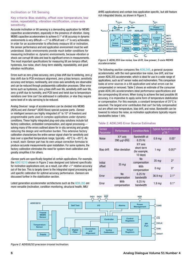
Latest generation accelerometer architectures such as the ADXL355 are more versatile (inclination, condition monitoring, structural health, IMU/
AHRS applications) and contain less application specific, but still feature rich integrated blocks, as shown in Figure 3.
ADC
ADC
ADC
ADCTempSensor
V1P8ANA
DigitalFilter
FIFO
PowerManagementVSUPPLY
VDDIO
LDO
V1P8DIG
LDO
XY
Z AnalogFilter
3-AxisSensor SCLK/VSSIO
MOSI/SDAMISO/ASEL
VSSIO VSS
INT1INT2
CS/SCL
ADXL355
DRDY
SerialI/O
ControlLogic
Figure 3. ADXL355 low noise, low drift, low power, 3-axis MEMS accelerometer.
The following section compares the ADXL345, a general-purpose accelerometer, with the next-generation low noise, low drift, and low power ADXL355 accelerometer, which is ideal for use in a wide range of applications, such as IoT sensor nodes and inclinometers. This comparison looks at error sources in a tilt application and what errors can be compensated or removed. Table 2 shows an estimate of the consumer grade ADXL345 accelerometers ideal performance specifications and the corresponding tilt errors. When trying to achieve the best possible tilt accuracy, it is imperative to apply some form of temperature stabilization or compensation. For this example, a constant temperature of 25°C is assumed. The largest error contributors that can’t be fully compensated out are offset over temperature, bias drift, and noise. Bandwidth can be lowered to reduce the noise, as inclination applications typically require bandwidths below 1 kHz.
Table 2. ADXL345 Error Source Estimates
Sensor Parameter
Performance Condition/NoteTypical Application Error
g Tilt °
NoiseX/Y axis
290 μg/√(Hz)Bandwidth at
6.25 Hz0.9 mg 0.05°
Bias drift Allan deviation
X/Y axis short-term
(for example, 10 days)
1 mg 0.057°
Initial offset
35 mg
No compensation
35 mg 2°
With compensation
0 mg 0°
ErrorNo
compensation6.25 Hz
bandwidth36.9 mg 2.1°
ErrorWith
compensation6.25 Hz
bandwidth1.9 mg 0.1°
ADIS16210
InclineCalibration
AlarmsI/OSelf Test
ControlRegisters
SPIPort
OutputRegisters
Correctionand
Alignment
DigitalFilter
TriaxialMEMSSensor
TemperatureSensor
Supply
PowerManagement
CS
SCLK
DIN
DOUT
GND
VDDDIO1 DIO2 RST
Controller
Figure 2. ADIS16210 precision triaxial inclination.
Analog Dialogue Volume 51 Number 4 7
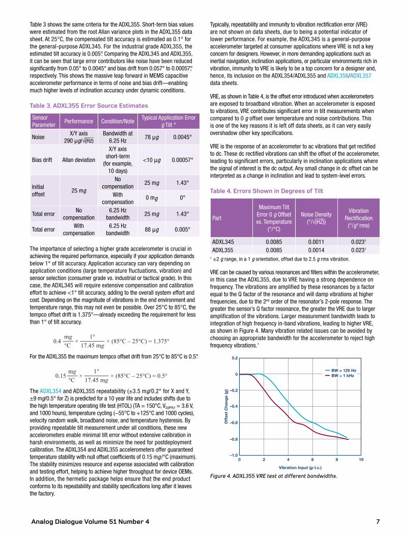
Table 3 shows the same criteria for the ADXL355. Short-term bias values were estimated from the root Allan variance plots in the ADXL355 data sheet. At 25°C, the compensated tilt accuracy is estimated as 0.1° for the general-purpose ADXL345. For the industrial grade ADXL355, the estimated tilt accuracy is 0.005°. Comparing the ADXL345 and ADXL355, it can be seen that large error contributors like noise have been reduced significantly from 0.05° to 0.0045° and bias drift from 0.057° to 0.00057°, respectively. This shows the massive leap forward in MEMS capacitive accelerometer performance in terms of noise and bias drift—enabling much higher levels of inclination accuracy under dynamic conditions.
Table 3. ADXL355 Error Source Estimates
Sensor Parameter
Performance Condition/NoteTypical Application Error
g Tilt °
NoiseX/Y axis
290 μg/√(Hz)Bandwidth at
6.25 Hz78 μg 0.0045°
Bias drift Allan deviation
X/Y axis short-term
(for example, 10 days)
<10 μg 0.00057°
Initial offset
25 mg
No compensation
25 mg 1.43°
With compensation
0 mg 0°
Total errorNo
compensation6.25 Hz
bandwidth25 mg 1.43°
Total errorWith
compensation6.25 Hz
bandwidth88 μg 0.005°
The importance of selecting a higher grade accelerometer is crucial in achieving the required performance, especially if your application demands below 1° of tilt accuracy. Application accuracy can vary depending on application conditions (large temperature fluctuations, vibration) and sensor selection (consumer grade vs. industrial or tactical grade). In this case, the ADXL345 will require extensive compensation and calibration effort to achieve <1° tilt accuracy, adding to the overall system effort and cost. Depending on the magnitude of vibrations in the end environment and temperature range, this may not even be possible. Over 25°C to 85°C, the tempco offset drift is 1.375°—already exceeding the requirement for less than 1° of tilt accuracy.
0.4 (85°C – 25°C) = 1.375°mg°C
× ×1°
17.45 mg
For the ADXL355 the maximum tempco offset drift from 25°C to 85°C is 0.5°.
0.15 (85°C – 25°C) = 0.5°mg°C
× ×1°
17.45 mg
The ADXL354 and ADXL355 repeatability (±3.5 mg/0.2° for X and Y, ±9 mg/0.5° for Z) is predicted for a 10 year life and includes shifts due to the high temperature operating life test (HTOL) (TA = 150°C, VSUPPLY = 3.6 V, and 1000 hours), temperature cycling (−55°C to +125°C and 1000 cycles), velocity random walk, broadband noise, and temperature hysteresis. By providing repeatable tilt measurement under all conditions, these new accelerometers enable minimal tilt error without extensive calibration in harsh environments, as well as minimize the need for postdeployment calibration. The ADXL354 and ADXL355 accelerometers offer guaranteed temperature stability with null offset coefficients of 0.15 mg /°C (maximum). The stability minimizes resource and expense associated with calibration and testing effort, helping to achieve higher throughput for device OEMs. In addition, the hermetic package helps ensure that the end product conforms to its repeatability and stability specifications long after it leaves the factory.
Typically, repeatability and immunity to vibration rectification error (VRE) are not shown on data sheets, due to being a potential indicator of lower performance. For example, the ADXL345 is a general-purpose accelerometer targeted at consumer applications where VRE is not a key concern for designers. However, in more demanding applications such as inertial navigation, inclination applications, or particular environments rich in vibration, immunity to VRE is likely to be a top concern for a designer and, hence, its inclusion on the ADXL354/ADXL355 and ADXL356/ADXL357 data sheets.
VRE, as shown in Table 4, is the offset error introduced when accelerometers are exposed to broadband vibration. When an accelerometer is exposed to vibrations, VRE contributes significant error in tilt measurements when compared to 0 g offset over temperature and noise contributions. This is one of the key reasons it is left off data sheets, as it can very easily overshadow other key specifications.
VRE is the response of an accelerometer to ac vibrations that get rectified to dc. These dc rectified vibrations can shift the offset of the accelerometer, leading to significant errors, particularly in inclination applications where the signal of interest is the dc output. Any small change in dc offset can be interpreted as a change in inclination and lead to system-level errors.
Table 4. Errors Shown in Degrees of Tilt
Part
Maximum Tilt Error 0 g Offset vs. Temperature
(°/°C)
Noise Density (°/√(HZ))
Vibration Rectification
(°/g 2 rms)
ADXL345 0.0085 0.0011 0.0231
ADXL355 0.0085 0.0014 0.0231
1 ±2 g range, in a 1 g orientation, offset due to 2.5 g rms vibration.
VRE can be caused by various resonances and filters within the accelerometer, in this case the ADXL355, due to VRE having a strong dependence on frequency. The vibrations are amplified by these resonances by a factor equal to the Q factor of the resonance and will damp vibrations at higher frequencies, due to the 2nd order of the resonator’s 2-pole response. The greater the sensor’s Q factor resonance, the greater the VRE due to larger amplification of the vibrations. Larger measurement bandwidth leads to integration of high frequency in-band vibrations, leading to higher VRE, as shown in Figure 4. Many vibration related issues can be avoided by choosing an appropriate bandwidth for the accelerometer to reject high frequency vibrations.1
–1.00
Off
set
Ch
ang
e (g
)
Vibration Input (g-l.c.)
0.2
0
–0.2
–0.4
–0.6
–0.8
2 4 6 8 10
BW = 125 Hz BW = 1 kHz
Figure 4. ADXL355 VRE test at different bandwidths.
Analog Dialogue Volume 51 Number 48
Static tilt measurements typically require low g accelerometers around ±1 g to ±2 g, with bandwidths less than 1.5 kHz. The analog output ADXL354 and the digital output ADXL355 are low noise density (20 μg/√Hz and 25 μg/√Hz respectively), low 0 g offset drift, low power, 3-axis accelerometers with integrated temperature sensors and selectable measurement ranges, as shown in Table 5.
Table 5. ADXL354/ADXL355/ADXL356/ADXL357 Measure-ment Ranges
Part Measurement Range (g) Bandwidth (kHz)ADXL354B ±2, ±4 1.5ADXL354C ±2, ±8 1.5ADXL355B ±2, ±4, ±8 1ADXL356B ±10, ±20 1.5ADXL356C ±10, ±40 1.5ADXL357B ±10.24, ±20.48, ±40.96 1
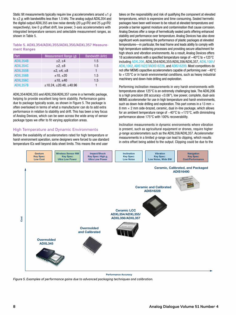
ADXL354/ADXL355 and ADXL356/ADXL357 come in a hermetic package, helping to provide excellent long-term stability. Performance gains due to package typically scale, as shown in Figure 5. The package is often overlooked in terms of what a manufacturer can do to add extra performance in relation to stability and drift. This has been a key focus of Analog Devices, which can be seen across the wide array of sensor package types we offer to fit varying application areas.
High Temperature and Dynamic EnvironmentsBefore the availability of accelerometers rated for high temperature or harsh environment operation, some designers were forced to use standard temperature ICs well beyond data sheet limits. This means the end user
takes on the responsibility and risk of qualifying the component at elevated temperatures, which is expensive and time consuming. Sealed hermetic packages have been well known to be robust at elevated temperatures and provide a barrier against moisture and contamination that cause corrosion. Analog Devices offer a range of hermetically sealed parts offering enhanced stability and performance over temperature. Analog Devices has also done significant work examining the performance of plastic packages at elevated temperatures—in particular, the lead frame and leads ability to comply with high temperature soldering processes and providing secure attachment for high shock and vibration environments. As a result, Analog Devices offers 18 accelerometers with a specified temperature range of −40°C to +125°C including ADXL206, ADXL354/ADXL355/ADXL356/ADXL357, ADXL1001/ADXL1002, ADIS16227/ADIS16228, and ADIS16209. Most competitors do not offer MEMS capacitive accelerometers capable of performing over −40°C to +125°C or in harsh environmental conditions, such as heavy industrial machinery and down-hole drilling and exploration.
Performing inclination measurements in very harsh environments with temperatures above 125°C is an extremely challenging task. The ADXL206 is a high precision (tilt accuracy <0.06°), low power, complete, dual-axis MEMS accelerometer for use in high temperature and harsh environments, such as down-hole drilling and exploration. This part comes in a 13 mm × 8 mm × 2 mm side-brazed, ceramic, dual in-line package, which allows for an ambient temperature range of −40°C to +175°C, with diminishing performance above 175°C with 100% recoverability.
Inclination measurements in dynamic environments where vibration is present, such as agricultural equipment or drones, require higher g-range accelerometers such as the ADXL356/ADXL357. Accelerometer measurements in a limited g-range can lead to clipping, which results in extra offset being added to the output. Clipping could be due to the
Performance Accuracy
GestureKey Spec:Low Cost
Impact/ShockKey Spec: High g,Ultra Low Power
InclinationKey Spec:Low Noise
VibrationKey Spec:
Low Noise, Wide BW
NavigationKey Spec:
Cost/Performance
Wireless Sensor NWKey Spec:
Ultra Low Power
Cos
t
OvermoldedADXL345
Overmoldedand Calibrated
Ceramic LCCADXL354/ADXL355/ADXL356/ADXL357
Ceramic and CalibratedADIS16228
Ceramic, Calibrated, and PackagedADIS16490
Figure 5. Examples of performance gains due to advanced packaging techniques and calibration.

Analog Dialogue Volume 51 Number 4 9
sensitive axis being in the 1 g field of gravity or due to shocks with fast rise times and slow decay. With a higher g-range, accelerometer clipping is reduced, thus reducing offset leading to better inclination accuracy in dynamic applications.
Figure 6 shows a g-range limited measurement from the ADXL356 Z-axis, with 1 g already being present in this range of measurement. Figure 7 shows the same measurement but with the g-range extended from ±10 g to ±40 g. It can be clearly seen that the offset due to clipping is significantly reduced by extending the g-range of the accelerometer.
The ADXL354/ADXL355 and ADXL356/ADXL357 offer superior vibration rectification, long-term repeatability, and low noise performance in a small form factor and are ideally suited for tilt/inclination sensing in both static and dynamic environments.
0.20
–0.20
–0.15
–0.10
–0.05
0
0.05
0.10
0.15
0 108642
Off
set
Sh
ift
(g)
Input Vibration (g rms)
Figure 6. ADXL356 VRE, Z-axis offset from 1 g, ±10 g-range, Z-axis orientation = 1 g.
Off
set
Sh
ift
(g)
Input Vibration (g rms)
0.2
–0.2
–0.1
0
0.1
0 252015105
Figure 7. ADXL356 VRE, Z-axis offset from 1 g, ±40 g-range, Z-axis orientation = 1 g.
Stabilization
Key criteria: Noise density, velocity random walk, in-run bias stability, bias repeatability, and bandwidth.Detecting and understanding motion can add value to many applications. Value arises from harnessing the motion that a system experiences and translating it into improved performance (reduced response time, higher precision, faster speed of operation), enhanced safety or reliability (system
shut-off in dangerous situations), or other added-value features. There is a large class of stabilization applications that require the combination of gyroscopes with accelerometers (sensor fusion), as shown in Figure 8, due to the complexity of motion—for example, in UAV-based surveillance equipment and antenna pointing systems used on ships.2
I/OSelf Test
Triaxial Gyroscope
Triaxial Accel
Temp
VDD
VDDRTC
DOUT
DIN
SCLK
CS
GND
VDDRSTDIO4DIO3DIO2DIO1
Clock
Controller Calibrationand Filters
SPI
Output Data
Registers
User Control
Registers
Alarms PowerManagement
ADIS16490/ADIS16495/ADIS16497
Figure 8. Six degrees of freedom IMU.
Six degrees of freedom IMUs use multiple sensors so they can compensate for each other’s weaknesses. What may seem like simple inertial motion on one or two axes can actually require accelerometer and gyroscope sensor fusion, in order to compensate for vibration, gravity, and other influences that an accelerometer or gyroscope alone would not be able to accurately measure. Accelerometer data consists of a gravity component and motion acceleration. These cannot be separated, but a gyroscope can be used to help remove the gravity component from the accelerometer output. The error due to the gravity component of the accelerometer data can quickly become large after the required integration process to determine position from acceleration. Due to accumulating error, a gyroscope alone is not sufficient for determining position. Gyroscopes do not sense gravity, so they can be used as a support sensor along with an accelerometer.
In stabilization applications the MEMS sensor must provide accurate measurements of the platforms orientation, particularly when it is in motion. A block diagram of a typical platform stabilization platform system utilizing servo motors for angular motion correction is shown in Figure 9. The feedback/servo motor controller translates the orientation sensors data into corrective control signals for the servo motors.
OrientationCommand
hMEMS(n) OrientationSensor
MEMS SensorPhysicallyMounted tothe InstrumentPlatform
ServoController
Motor
Figure 9. Basic platform stabilization system.3
The end application will dictate the level of accuracy required, and the quality of sensor chosen whether consumer or industrial grade will determine whether this is achievable or not. It is important to distinguish between consumer grade devices and industrial grade devices, and this can sometimes require careful consideration as the differences can be subtle. Table 6 shows the key differences between a consumer grade and midlevel industrial grade accelerometer integrated into an IMU.
Analog Dialogue Volume 51 Number 410
Table 6. Industrial MEMS Devices Offer Extensive Characterization of All Known Potential Error Sources and Achieve More Than Order of Magnitude Precision Improvement vs. Consumer2
Accelerometer Parameter
Typical Industrial Specification
Improvement Over Typical Consumer
DeviceDynamic range Up to 40 g 3×Noise density 25 μg/√Hz 10×Velocity random walk 0.03 m/s/√Hz 10×In-run bias stability 10 μg 10×Bias repeatability 25 mg 100×–3 dB bandwidth 500 Hz 2×
In some cases where conditions are benign and imprecise data is acceptable, a low precision device can provide adequate performance. However, the demands on the sensor in dynamic conditions grow rapidly and lower precision parts suffer greatly due to not being able to reduce vibration effects from actual measurements or temperature effects, therefore struggling to measure below 3° to 5° of pointing accuracy. Most low end consumer devices do not provide specifications for parameters such as vibration rectification, angular random walk, and other parameters that actually can be the largest error sources in industrial applications.
In order to measure from 1° down to 0.1° of pointing accuracy in dynamic environments, a designer’s part selection must focus on the sensors ability to reject drift error over temperature and vibration influences. While sensor filtering and algorithms (sensor fusion) are a critical element in achieving improved performance, they are not capable of eliminating performance gaps from a consumer grade to industrial grade sensor. Analog Devices new class of industrial IMUs achieve performance close to what was used in previous generation missile guidance systems. Parts such as the ADIS1646x and the announced ADIS1647x can provide precision motion sensing in standard and mini IMU form factors, opening up what used to be a niche application area.
In part 2 of this article we will continue to explore key performance characteristics of MEMS accelerometers and how to they relate to applications areas such as wearable devices, condition-based monitoring, and IoT, including structural health monitoring and asset health monitoring.
References¹ Long Pham and Anthony DeSimone. “Vibration Rectification in MEMS
Accelerometers.” Analog Devices, Inc., 2017.
² Bob Scannell. “High Performance Inertial Sensors Propelling the Internet of Moving Things.” Analog Devices, Inc., 2017.
³ Mark Looney. “Analyzing Frequency Response of Inertial MEMS in Stabilization Systems.” Analog Dialogue, Vol. 46, 2012.
Chris Murphy [[email protected]] is an applications engineer with the European Centralized Applications Center, based in Dublin, Ireland. He has worked for Analog Devices since 2012, providing design support on motor control and industrial automation products. He holds a master’s of engineering in electronics by research and a bachelor’s of engineering in computer engineering.
Chris Murphy
Also by this Author:
Accelerometer Tilt Measure Over Tem-perature and in the Presence of Vibration
Volume 51, Number 4

Analog Dialogue Volume 51 Number 4 11
Share on
2010 to 2015
>500 V
250 V to 500 V
125 V to 250 V
<125 V
By 2020
>500 V
250 V to 500 V
125 V to 250 V
<125 V
Figure 2. Forward looking charged device model sensitivity distribu-tion groups (Copyright©2016 EOS/ESD Association, Inc.).
Why is this change important to discuss? It points out the need for a con-sistent way to test CDM across the electronics industry without some of the inconsistencies created by having multiple test standards. It is more important now than ever to ensure manufacturing is properly prepared for the CDM roadmap discussed by the ESDA. One critical piece of that preparation is ensuring that manufacturing receives consistent data from each semiconductor manufacturer on the CDM robustness level of their devices. The need for a harmonized CDM standard has never been greater. This, coupled with continued technology advancements, may also drive higher IO performance. This need for higher IO performance (and its need for reduced pin capacitance) may leave an IC designer with no other option other than lowering the target levels, which in turn demands a more pre-cise measurement (which is addressed within ANSI/ESDA/JEDEC JS-002).
A New Joint StandardPrior to ANSI/ESDA/JEDEC JS-002, there were four existing standards: the legacy JEDEC (JESD22-C101),5 ESDA S5.3.1,6 AEC Q100-011,7 and EIAJ ED-4701/300-2 standards.8 ANSI/ESDA/JEDEC JS-002 (charged device model, device level)9 represents a major first push toward harmonization of these four existing standards into a single standard. While all of these methods produce valuable information, the presence of several standards is not a benefit to the industry. The different methods often produce different passing levels, and the presence of several standards requires manufac-turers to support multiple test methods with no increase in meaningful information. Therefore, it is vitally important that a single measurement level of an IC’s charged device immunity is well known to ensure the CDM
Charged device model (CDM) ESD is considered to be the primary real-world ESD model for representing ESD charging and rapid discharge and is the best representation of what can occur in automated handling equip-ment used in manufacturing and the assembly of integrated circuits (ICs) today. It is well known that the largest cause by far of ESD damage to an IC during device handling in a manufacturing environment is from charged device events.1
Charged Device Model RoadmapWith the ever increasing demand for higher speed IOs in ICs and the need for packing more functionality into a single package driving larger package sizes, efforts to maintain the recommended target CDM levels as discussed in JEP1572, 3 will be a challenge. It should also be noted that while technol-ogy scaling may not have a direct impact on target levels (at least down to 14 nm), the introduction of improved transistor performance in these advanced technologies can also enable higher IO performance (transfer rates), which can make achieving current target levels difficult for the IO designer as well. As a result of the inconsistent charging resistors between different testers, looking at published, ESD Association (ESDA) roadmaps out through the year 20204 suggests that CDM target levels will need to be reduced again, as shown in Figure 1.
500 V
250 V
125 V
0 V2010 2015
Current Target Level
CDM Forward Looking Roadmap (Typical Min to Max)
Projected Target Level
2020
*Includes Process Specific Measures to Avoid Charging or Discharging**Includes Process Specific Measures to Avoid Charging and Discharging
CDM Control MethodEstimated Levels
S20.20 (200 V)
Process SpecificMeasures* (100 V)
Charge/DischargeMeasurements atEach Process Step**(50 V)
Figure 1. Charged device model sensitivity limits projections from 2010 and beyond (Copyright ©2016 EOS/ESD Association, Inc.).
While a quick look at Figure 1 would not suggest a significant change in the range of CDM target levels, a further look at data supplied by the ESDA and shown in Figure 2 shows that there is expected to be a significant change in the distribution of CDM ESD target levels.
A Look at the New ANSI/ESDA/JEDEC JS-002 CDM Test StandardBy Alan Righter, Brett Carn, and The EOS/ESD Association
Analog Dialogue Volume 51 Number 412
ESD design strategy has been implemented correctly and that the IC’s charged device immunity is matched to the level of ESD control in the manufacturing environment to which it will be exposed.
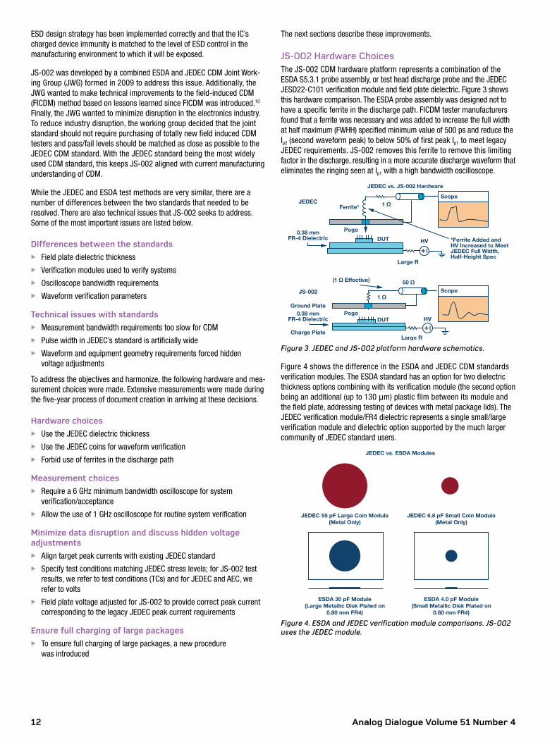
JS-002 was developed by a combined ESDA and JEDEC CDM Joint Work-ing Group (JWG) formed in 2009 to address this issue. Additionally, the JWG wanted to make technical improvements to the field-induced CDM (FICDM) method based on lessons learned since FICDM was introduced.10 Finally, the JWG wanted to minimize disruption in the electronics industry. To reduce industry disruption, the working group decided that the joint standard should not require purchasing of totally new field induced CDM testers and pass/fail levels should be matched as close as possible to the JEDEC CDM standard. With the JEDEC standard being the most widely used CDM standard, this keeps JS-002 aligned with current manufacturing understanding of CDM.
While the JEDEC and ESDA test methods are very similar, there are a number of differences between the two standards that needed to be resolved. There are also technical issues that JS-002 seeks to address. Some of the most important issues are listed below.
Differences between the standards X Field plate dielectric thickness X Verification modules used to verify systems X Oscilloscope bandwidth requirements X Waveform verification parameters
Technical issues with standards X Measurement bandwidth requirements too slow for CDM X Pulse width in JEDEC’s standard is artificially wide X Waveform and equipment geometry requirements forced hidden
voltage adjustments
To address the objectives and harmonize, the following hardware and mea-surement choices were made. Extensive measurements were made during the five-year process of document creation in arriving at these decisions.
Hardware choices X Use the JEDEC dielectric thickness X Use the JEDEC coins for waveform verification X Forbid use of ferrites in the discharge path
Measurement choices X Require a 6 GHz minimum bandwidth oscilloscope for system
verification/acceptance X Allow the use of 1 GHz oscilloscope for routine system verification
Minimize data disruption and discuss hidden voltage adjustments
X Align target peak currents with existing JEDEC standard X Specify test conditions matching JEDEC stress levels; for JS-002 test
results, we refer to test conditions (TCs) and for JEDEC and AEC, we refer to volts
X Field plate voltage adjusted for JS-002 to provide correct peak current corresponding to the legacy JEDEC peak current requirements
Ensure full charging of large packages X To ensure full charging of large packages, a new procedure
was introduced
The next sections describe these improvements.
JS-002 Hardware ChoicesThe JS-002 CDM hardware platform represents a combination of the ESDA S5.3.1 probe assembly, or test head discharge probe and the JEDEC JESD22-C101 verification module and field plate dielectric. Figure 3 shows this hardware comparison. The ESDA probe assembly was designed not to have a specific ferrite in the discharge path. FICDM tester manufacturers found that a ferrite was necessary and was added to increase the full width at half maximum (FWHH) specified minimum value of 500 ps and reduce the Ip2 (second waveform peak) to below 50% of first peak Ip1 to meet legacy JEDEC requirements. JS-002 removes this ferrite to remove this limiting factor in the discharge, resulting in a more accurate discharge waveform that eliminates the ringing seen at Ip1 with a high bandwidth oscilloscope.
Scope
JEDEC vs. JS-002 Hardware
JEDEC
JS-002
Ferrite*
*Ferrite Added andHV Increased to MeetJEDEC Full Width, Half-Height Spec
Large R
Large R
0.38 mmFR-4 Dielectric
0.38 mmFR-4 Dielectric
Charge Plate
Ground Plate
Pogo
Pogo
DUT
1 Ω
1 Ω
50 Ω(1 Ω Effective)
DUT
HV
HV
Scope
Figure 3. JEDEC and JS-002 platform hardware schematics.
Figure 4 shows the difference in the ESDA and JEDEC CDM standards verification modules. The ESDA standard has an option for two dielectric thickness options combining with its verification module (the second option being an additional (up to 130 μm) plastic film between its module and the field plate, addressing testing of devices with metal package lids). The JEDEC verification module/FR4 dielectric represents a single small/large verification module and dielectric option supported by the much larger community of JEDEC standard users.
JEDEC vs. ESDA Modules
JEDEC 55 pF Large Coin Module(Metal Only)
JEDEC 6.8 pF Small Coin Module(Metal Only)
ESDA 30 pF Module(Large Metallic Disk Plated on
0.80 mm FR4)
ESDA 4.0 pF Module(Small Metallic Disk Plated on
0.80 mm FR4)
Figure 4. ESDA and JEDEC verification module comparisons. JS-002 uses the JEDEC module.
Analog Dialogue Volume 51 Number 4 13
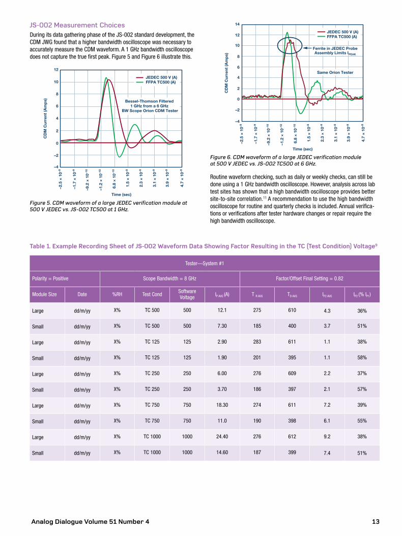
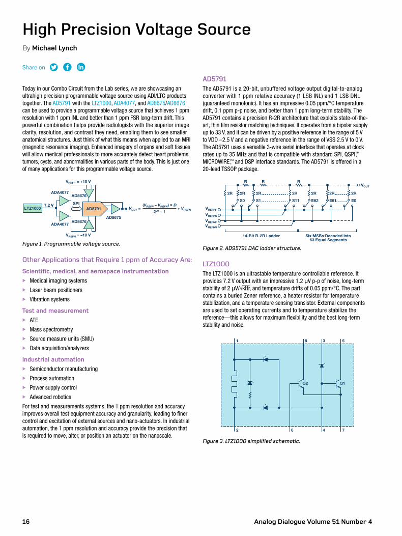
JS-002 Measurement ChoicesDuring its data gathering phase of the JS-002 standard development, the CDM JWG found that a higher bandwidth oscilloscope was necessary to accurately measure the CDM waveform. A 1 GHz bandwidth oscilloscope does not capture the true first peak. Figure 5 and Figure 6 illustrate this.
Time (sec)
–2.5
× 1
0–9
–1.7
× 1
0–9
–9.2
× 1
0–10
–1.2
× 1
0–10
6.8
× 1
0–10
1.5
× 1
0–9
2.3
× 1
0–9
3.1
× 1
0–9
3.9
× 1
0–9
4.7
× 1
0–9
–4
0
–2
2
12
10
8
6
4
CD
M C
urre
nt (A
mp
s) Bessel-Thomson Filtered 1 GHz from a 6 GHz
BW Scope Orion CDM Tester
JEDEC 500 V (A)FFPA TC500 (A)
Figure 5. CDM waveform of a large JEDEC verification module at 500 V JEDEC vs. JS-002 TC500 at 1 GHz.
Time (sec)
–2.5
× 1
0–9
–1.7
× 1
0–9
–9.2
× 1
0–10
–1.2
× 1
0–10
6.8
× 1
0–10
1.5
× 1
0–9
2.3
× 1
0–9
3.1
× 1
0–9
3.9
× 1
0–9
4.7
× 1
0–9
–4
0
–2
2
12
14
10
8
6
4
CD
M C
urre
nt (A
mp
s)
Same Orion Tester
Ferrite in JEDEC ProbeAssembly Limits IPEAK
JEDEC 500 V (A)FFPA TC500 (A)
Figure 6. CDM waveform of a large JEDEC verification module at 500 V JEDEC vs. JS-002 TC500 at 6 GHz.
Routine waveform checking, such as daily or weekly checks, can still be done using a 1 GHz bandwidth oscilloscope. However, analysis across lab test sites has shown that a high bandwidth oscilloscope provides better site-to-site correlation.11 A recommendation to use the high bandwidth oscilloscope for routine and quarterly checks is included. Annual verifica-tions or verifications after tester hardware changes or repair require the high bandwidth oscilloscope.
Table 1. Example Recording Sheet of JS-002 Waveform Data Showing Factor Resulting in the TC (Test Condition) Voltage9
Tester—System #1
Polarity = Positive Scope Bandwidth = 8 GHz Factor/Offset Final Setting = 0.82
Module Size Date %RH Test Cond Software Voltage IP AVG (A) T R AVG TD AVG IP2 AVG IP2 (% IP1)
Large dd/m/yy X% TC 500 500 12.1 275 610 4.3 36%
Small dd/m/yy X% TC 500 500 7.30 185 400 3.7 51%
Large dd/m/yy X% TC 125 125 2.90 283 611 1.1 38%
Small dd/m/yy X% TC 125 125 1.90 201 395 1.1 58%
Large dd/m/yy X% TC 250 250 6.00 276 609 2.2 37%
Small dd/m/yy X% TC 250 250 3.70 186 397 2.1 57%
Large dd/m/yy X% TC 750 750 18.30 274 611 7.2 39%
Small dd/m/yy X% TC 750 750 11.0 190 398 6.1 55%
Large dd/m/yy X% TC 1000 1000 24.40 276 612 9.2 38%
Small dd/m/yy X% TC 1000 1000 14.60 187 399 7.4 51%

Analog Dialogue Volume 51 Number 414
Tester CDM Voltage SettingsThe CDM JWG also discovered that across tester platforms significant variation in the actual plate voltage setting (for example, 100 V or more at a specific voltage setting) was needed to obtain standard test waveform compliance in the previous ESDA and JEDEC standards. This was not described in any of the standards. JS-002 is unique in determining the offset or factor required to scale first peak current (and voltage repre-sented by a test condition) to the JEDEC peak current levels. Annex G of JS-002 describes this in detail. Table 1 shows an example of verification data incorporating this feature.
Ensuring Full Charging of Very Large Devices at a Set Test ConditionDuring the data gathering phase of the JS-002 development, another tester-dependent issue was discovered whereby some test systems were not fully charging large verification modules or devices to their set voltage before discharging. It was found that the high value field plate charging resistor (a series resistor between the charging supply and the field plate) was not consistent between test systems, affecting the delay time required for full plate voltage charging. As a result, the first peak discharge currents could vary among testers, affecting the pass/fail CDM classification espe-cially for large devices.
Because of this, Informative Annex H (“Determining the Appropriate Charge Delay for Full Charging of a Large Module or Device”) was written to describe a procedure for determination of the delay time needed to fully charge a device. An appropriate charge delay time is reached when a peak current saturation point (where Ip attains a basically constant value independent of longer decay time settings) is found to occur, as shown in Figure 7. Determining this delay time ensures that very large devices are fully charged to a set test condition prior to discharge.
Time Delay (ms)
0 100 200 300 400 500 6004.0
4.2
4.4
4.6
6.0
5.8
5.6
5.4
5.2
5.0
4.8
Ip (A
)
Saturation Point
Figure 7. Example peak current vs. charge time delay plot showing the saturation point/charge time delay.9
Phase-In of JS-002 in the Electronics IndustryThe JS-002 standard replaces and obsoletes the ESDA S5.3.1 CDM standard for those companies using S5.3.1 as the standard. For those previously using JESD22-C101, the JEDEC reliability test specifications document JESD47 (specifying all reliability test methods for JEDEC electronic components) was recently updated to specify JS-002 in place of JESD22-C101 (in late 2016). A phase-in period is now in effect regarding JEDEC member company transition to JS-002. Many companies, including ADI and Intel, have already transitioned to testing using JS-002 for all new products.
The International Electrotechnical Commission (IEC) recently approved and updated its CDM test standard, IS 60749-28.12 This standard incorporates JS-002 in its entirety as its specified test standard.
The Automotive Electronics Council (AEC) currently has a CDM subteam committee updating the Q100-011 (integrated circuit) and Q101-005 (passive components) automotive device CDM standard documents to incorporate JS-002, with AEC specified test use conditions. These are expected to be completed and approved by the end of 2017.
SummaryAs we look at the CDM ESD roadmap provided by the ESDA, CDM target levels will continue to be lowered, driven by higher IO performance. Man-ufacturing awareness of device level CDM ESD withstand voltage is more critical than ever and cannot be accurately communicated by inconsistent product CDM results coming from different CDM ESD standards. ANSI/ESDA/JEDEC JS-002 has the opportunity to be the first true industry-wide CDM test standard. The removal of inductance in the CDM test head dis-charge path significantly improves the quality of the discharge waveform. The introductions of a high bandwidth oscilloscope for verification, the increase to five test condition waveform verification levels, and an assur-ance of the correct charging delay time all significantly reduce cross-lab variation in test results—improving repeatability from site to site. This is critical to ensure consistent data is supplied to manufacturing. With JS-002 acceptance across the electronics industry, the industry will be in a much better position to address the ESD control challenges ahead.
References1 Roger J. Peirce. “The Most Common Causes of ESD Damage.”
Evaluation Engineering, November, 2002.
2 Industry Council on ESD Target Levels. “Industry Council White Paper 2: A Case for Lowering Component Level CDM ESD Specifications and Requirements.” EOS/ESD Association, Inc., April, 2010.
3 “JEP157: Recommended ESD-CDM Target Levels.” JEDEC, October, 2009.
4 EOS/ESD Association Roadmap.
5. “JESD22-C101F: Field-Induced Charged-Device Model Test Method for Electrostatic Discharge Withstand Thresholds of Microelectronic Components.” JEDEC, October, 2013.
6. “ANSI/ESD S5.3.1: Electrostatic Discharge Sensitivity Testing—Charged Device Model (CDM) Component Level.” EOS/ESD Association, December 2009.
7 “AEC-Q100-011: Charged Device Model (CDM) Electrostatic Discharge Test.” Automotive Electronics Council, July 2012.
8 “EIAJ ED-4701/300-2, Test Method 305: Charged Device Model Electrostatic Discharge (CDM-ESD).” Japan Electronics and Information Technology Industries Association, June, 2004.
9 “ANSI/ESDA/JEDEC JS-002-2014: Charged Device Model (CDM) Device Level.” EOS/ESD Association, April, 2015.
10 Alan W. Righter, Terry Welsher, and Marti Ferris. “Progress Towards a Joint ESDA/JEDEC CDM Standard: Methods, Experiments, and Results.” EOS/ESD Symposium, September, 2012.
11 Theo Smedes, Michal Polweski, Arjan van IJzerloo, Jean-Luc Lefebvre, and Marcel Dekker. “Pitfalls for CDM Calibration Procedures.” EOS/ESD Symposium, October, 2010.
12 “IEC IS 60749-28, Electrostatic Discharge (ESD) Sensitivity Testing– Charged Device Model (CDM)–Device Level.” International Electrotechnical Commission, 2017.

Analog Dialogue Volume 51 Number 4 15
Alan [[email protected]] is a senior staff ESD engineer in the corporate ESD department at Analog Devices, San Jose, CA. He works with ADI design/product engineering teams worldwide on whole chip ESD planning/design, ESD testing, ESD failure analysis, and EOS issues with internal and external customers. Prior to ADI, Alan was with Sandia National Laboratories, Albuquerque, NM for 13 years, where he was involved in IC design, test, product engineering, reliability testing, and failure analysis. Alan completed his B.S.E.E. and M.S.E.E. at Arizona State University in 1982 and 1984, respectively, and his Ph.D. at the University of New Mexico in 1996. In 2007, Alan joined all Standards Device Testing Working Groups (WG5.x) and is also a member of Systems and Simulators WG 14. He was appointed chair of WG 5.3.1, Charged Device Model, in 2008 and currently serves as ESDA Chairperson of the expanded Joint (ESDA/JEDEC) CDM Working Group, which recently completed the new ESDA/JEDEC Joint Standard JS-002. Alan is also currently Vice President of the ESD Association. Alan has been active in the EOS/ESD Symposium as author/co-author of 10 articles, and he is also currently ESDA Events Director. Alan also is active in the Industry Council on ESD Target Levels.
Alan Righter
Brett Carn [[email protected]] joined Intel Corporation in 1999 and is a principal engineer in the Corporate Quality Network. He has actively worked in the field of device level ESD at Intel. In that role, Brett chairs the Intel ESD Council overseeing component level ESD and latch-up testing across all Intel sites worldwide, defining all internal test specifications, reviewing all Intel ESD design rules, overseeing/defining the ESD target levels for all Intel products worldwide, and leading postsilicon ESD debug on many products. In more recent years, Brett has also been actively involved with addressing EOS challenges. Prior to joining Intel, he worked for Lattice Semiconductor for 13 years, where he started working on ESD in the early 1990s. Since 2007, Brett has been a member of the Industry Council on ESD Target Levels and has helped author several white papers, and also served as the lead editor on four white papers. Brett is an active member of the ESDA and a current member of the ESDA Board of Directors. Brett is also a member of the ESDA Education Council, overseeing all online training, and is the current chair of the Technical and Advisory Support (TAS) Committee and a member of several ESDA working groups. Brett received his B.S. in electrical engineering from Portland State University in 1986.
Brett Carn
The EOS/ESD Association is the largest industry group dedicated to advancing the theory and the practice of ESD avoidance, with more than 2000 members worldwide. Readers can learn more about the association and its work at http://www.esda.org.
The EOS/ESD Association
Analog Dialogue Volume 51 Number 416
Share on
AD5791The AD5791 is a 20-bit, unbuffered voltage output digital-to-analog converter with 1 ppm relative accuracy (1 LSB INL) and 1 LSB DNL (guaranteed monotonic). It has an impressive 0.05 ppm/°C temperature drift, 0.1 ppm p-p noise, and better than 1 ppm long-term stability. The AD5791 contains a precision R-2R architecture that exploits state-of-the-art, thin film resistor matching techniques. It operates from a bipolar supply up to 33 V, and it can be driven by a positive reference in the range of 5 V to VDD –2.5 V and a negative reference in the range of VSS 2.5 V to 0 V. The AD5791 uses a versatile 3-wire serial interface that operates at clock rates up to 35 MHz and that is compatible with standard SPI, QSPI™, MICROWIRE™, and DSP interface standards. The AD5791 is offered in a 20-lead TSSOP package.
VREFPF
VOUT
Six MSBs Decoded into63 Equal Segments
14-Bit R-2R Ladder
2R
R R R
2R 2R 2R 2R 2R 2R
S0 S1 S11 E62 E61 E0
VREFPS
VREFNF
VREFNS
Figure 2. AD95791 DAC ladder structure.
LTZ1000The LTZ1000 is an ultrastable temperature controllable reference. It provides 7.2 V output with an impressive 1.2 µV p-p of noise, long-term stability of 2 μV/√kHr, and temperature drifts of 0.05 ppm/°C. The part contains a buried Zener reference, a heater resistor for temperature stabilization, and a temperature sensing transistor. External components are used to set operating currents and to temperature stabilize the reference—this allows for maximum flexibility and the best long-term stability and noise.
1 8 3 5
2 6
.
.
. Q2 Q1
4 7
Figure 3. LTZ1000 simplified schematic.
Today in our Combo Circuit from the Lab series, we are showcasing an ultrahigh precision programmable voltage source using ADI/LTC products together. The AD5791 with the LTZ1000, ADA4077, and AD8675/AD8676 can be used to provide a programmable voltage source that achieves 1 ppm resolution with 1 ppm INL and better than 1 ppm FSR long-term drift. This powerful combination helps provide radiologists with the superior image clarity, resolution, and contrast they need, enabling them to see smaller anatomical structures. Just think of what this means when applied to an MRI (magnetic resonance imaging). Enhanced imagery of organs and soft tissues will allow medical professionals to more accurately detect heart problems, tumors, cysts, and abnormalities in various parts of the body. This is just one of many applications for this programmable voltage source.
ADA4077
LTZ10007.2 V
VREFP = +10 V
VREFN = –10 V
AD8676
AD8676AD8675
ADA4077
SPIVOUT = + VREFN
(VREFP – VREFN) × D220 – 1
AD5791
Figure 1. Programmable voltage source.
Other Applications that Require 1 ppm of Accuracy Are:
Scientific, medical, and aerospace instrumentation X Medical imaging systems X Laser beam positioners X Vibration systems
Test and measurement X ATE X Mass spectrometry X Source measure units (SMU) X Data acquisition/analyzers
Industrial automation X Semiconductor manufacturing X Process automation X Power supply control X Advanced robotics
For test and measurements systems, the 1 ppm resolution and accuracy improves overall test equipment accuracy and granularity, leading to finer control and excitation of external sources and nano-actuators. In industrial automation, the 1 ppm resolution and accuracy provide the precision that is required to move, alter, or position an actuator on the nanoscale.
High Precision Voltage SourceBy Michael Lynch
Analog Dialogue Volume 51 Number 4 17
ADA4077The ADA4077 is a high precision, low noise operational amplifier with a combination of extremely low offset voltage and very low input bias currents. Unlike JFET amplifiers, the low bias and offset currents are relatively insensitive to ambient temperatures, even up to 125°C. Outputs are stable with capacitive loads of more than 1000 pF with no external compensation.
AD8675/AD8676The AD8675/AD8676 are precision, rail-to-rail operational amplifiers with ultralow offset, drift, and voltage noise combined with very low input bias currents over the full operating temperature range.
Some Circuit Considerations
NoiseLow frequency noise must be kept to a minimum to avoid impact on the dc performance of the circuit. In the 0.1 Hz to 10 Hz bandwidth, the AD5791 generates about 0.6 μV p-p noise, each ADA4077 will generate 0.25 μV p-p noise, the AD8675 will generate 0.1 μV p-p noise, and the LTZ1000 generates 1.2 μV p-p noise. Resistor values were chosen to ensure that their Johnson noise will not significantly add to the total noise level.
AD5791 Reference Buffer ConfigurationThe reference buffers used to drive the REFP and REFN pins of the AD5791 must be configured in unity gain. Any extra currents flowing through a gain setting resistor into the reference sense pins will degrade the accuracy of the DAC.
AD5791 INL SensitivityThe AD5791 INL performance is marginally sensitive to the input bias current of the amplifiers used as reference buffers. For this reason, amplifiers with low input bias currents were chosen.
ExtraINLError = 0.2 × IBIAS
INL – ppmIBIAS – nAVREF – Volts(VREFP – VREFN) 2
Temperature DriftTo maintain a low temperature drift coefficient for the entire system, the individual components chosen must have low temperature drift. The AD5791 has a TC of 0.05 ppm FSR/°C, the LTZ1000 offers a TC of 0.05 ppm/°C, and the ADA4077 and the AD8675 contribute 0.005 ppm FSR/°C and 0.01ppm FSR/°C, respectively.
Long-Term DriftLong-term drift is another important parameter that can cause significant accuracy limitations in systems. Long-term stability for the AD5791 is typically better than 0.1 ppm/1000 hours at 125°C. Long-term stability on the order of 1 μV per month can be achieved with the LTZ1000.
Days
0 10 20 30–2
2
0
LTZ1000 Long-Term Stability
(pp
m)
Figure 4. Long-term stability of a typical device from time = 0 with no preconditioning or aging.
Lab ResultsINL error was measured at ambient temperature in the lab by varying the input code to the AD5791 from zero-scale to full-scale with a code step of 5. The voltage at the output of the output buffer (AD8675) was recorded at each code using an 8.5 digit DVM. The results were well within the ±1 LSB specification.
0 200k 400k 600k 800k 1M–0.7
–0.6
–0.3
–0.4
–0.5
–0.2
–0.1
0.4
0.3
0.2
0.1
0
INL
Err
or
(LS
Bs)
Number of Samples
Figure 5. INL error of the high precision voltage source at ambient temperature.
Analog Dialogue Volume 51 Number 418
NoiseThe noise measured at mid-scale was 1.1 μV p-p and the noise measured at full scale was 3.7 μV p-p. The noise contribution from each voltage reference path is attenuated by the DAC when mid-scale code is selected—hence the lower noise figure for mid-scale code.
Time (Seconds)
0 1 2 3 4 5 6 7 8 9 10–2.0
–1.5
–1.0
–0.5
0
2.5
2.0
1.5
1.0
0.5
Out
put
Vo
ltag
e (µ
V)
Full Scale (V)Mid-Scale
Figure 6. Voltage noise in 0.1 Hz to 10 Hz bandwidth.
Long-Term DriftThe system long-term drift was measured at 25°C. The AD5791 was programmed to 5 V (¾ scale) and the output voltage was measured every 30 minutes over a period of 1000 hours. Drift values less than 1 ppm FSR were observed.
Elapsed Time (Hours)
0 100 200 300 400 500 600 700 800 900 1k–0.3
–0.2
–0.1
0
0.1
0.7
0.6
0.5
0.4
0.3
0.2
Dri
ft p
pm
FS
R
Figure 7. VOUT drift (ppm FSR).
ConclusionIn addition to ease of use, the AD5791 offers a guaranteed 1 ppm accuracy. However, selecting the correct components and voltage reference is critical to capitalize on the precision specifications of the AD5791. The low noise, low temperature drift, low long-term drift, and high precision of the LTZ1000, ADA4077, AD8676, and the AD8675 improve the system precision, stability, and repeatability over temperature and time.
Figure 8. EVAL-AD5791SDZ with LTZ1000 reference board.
Michael Lynch [[email protected]] is an applications engineer in the Linear and Precision Technology Group of Analog Devices. He received a B. Eng. degree in electronic engineering from the University of Limerick in 2003. He joined Analog Devices in 2009. Prior to joining Analog Devices, Michael worked as an implementation engineer for Intel.
Michael Lynch
Analog Dialogue Volume 51 Number 4 19
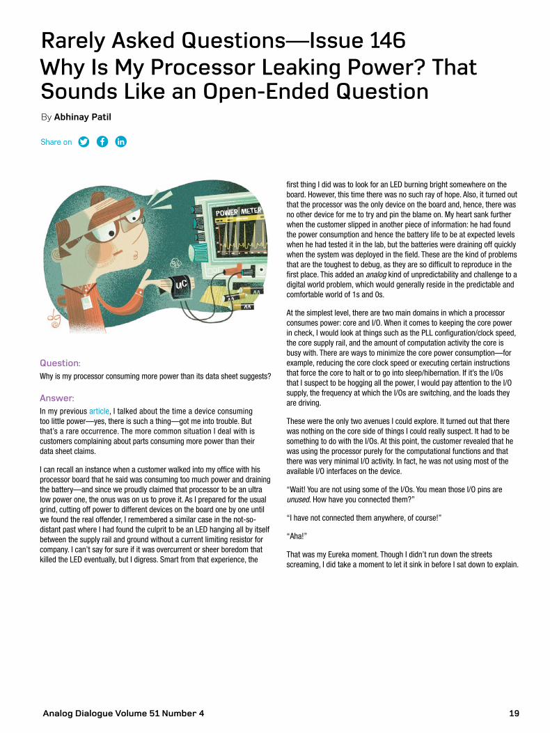
first thing I did was to look for an LED burning bright somewhere on the board. However, this time there was no such ray of hope. Also, it turned out that the processor was the only device on the board and, hence, there was no other device for me to try and pin the blame on. My heart sank further when the customer slipped in another piece of information: he had found the power consumption and hence the battery life to be at expected levels when he had tested it in the lab, but the batteries were draining off quickly when the system was deployed in the field. These are the kind of problems that are the toughest to debug, as they are so difficult to reproduce in the first place. This added an analog kind of unpredictability and challenge to a digital world problem, which would generally reside in the predictable and comfortable world of 1s and 0s.
At the simplest level, there are two main domains in which a processor consumes power: core and I/O. When it comes to keeping the core power in check, I would look at things such as the PLL configuration/clock speed, the core supply rail, and the amount of computation activity the core is busy with. There are ways to minimize the core power consumption—for example, reducing the core clock speed or executing certain instructions that force the core to halt or to go into sleep/hibernation. If it’s the I/Os that I suspect to be hogging all the power, I would pay attention to the I/O supply, the frequency at which the I/Os are switching, and the loads they are driving.
These were the only two avenues I could explore. It turned out that there was nothing on the core side of things I could really suspect. It had to be something to do with the I/Os. At this point, the customer revealed that he was using the processor purely for the computational functions and that there was very minimal I/O activity. In fact, he was not using most of the available I/O interfaces on the device.
“Wait! You are not using some of the I/Os. You mean those I/O pins are unused. How have you connected them?”
“I have not connected them anywhere, of course!”
“Aha!”
That was my Eureka moment. Though I didn’t run down the streets screaming, I did take a moment to let it sink in before I sat down to explain.
Question:Why is my processor consuming more power than its data sheet suggests?
Answer:In my previous article, I talked about the time a device consuming too little power—yes, there is such a thing—got me into trouble. But that’s a rare occurrence. The more common situation I deal with is customers complaining about parts consuming more power than their data sheet claims.
I can recall an instance when a customer walked into my office with his processor board that he said was consuming too much power and draining the battery—and since we proudly claimed that processor to be an ultra low power one, the onus was on us to prove it. As I prepared for the usual grind, cutting off power to different devices on the board one by one until we found the real offender, I remembered a similar case in the not-so-distant past where I had found the culprit to be an LED hanging all by itself between the supply rail and ground without a current limiting resistor for company. I can’t say for sure if it was overcurrent or sheer boredom that killed the LED eventually, but I digress. Smart from that experience, the
Rarely Asked Questions—Issue 146Why Is My Processor Leaking Power? That Sounds Like an Open-Ended QuestionBy Abhinay Patil
Share on
Analog Dialogue Volume 51 Number 420
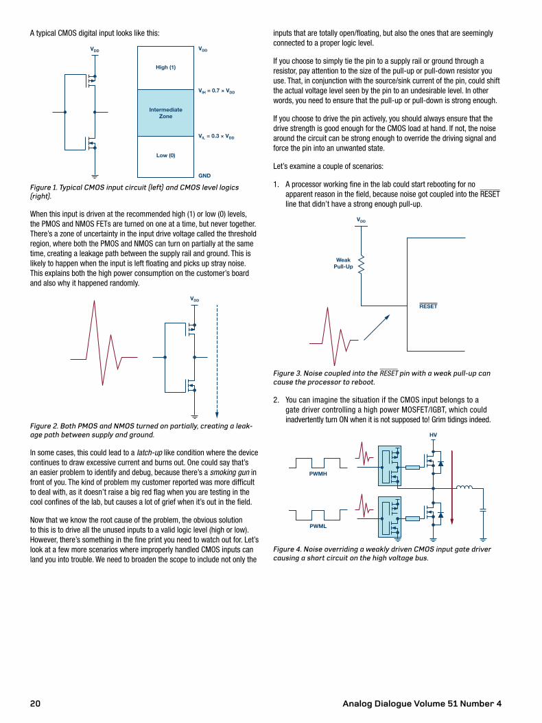
A typical CMOS digital input looks like this:
VDD VDD
VIH = 0.7 × VDD
VIL = 0.3 × VDD
GND
Low (0)
High (1)
IntermediateZone
Figure 1. Typical CMOS input circuit (left) and CMOS level logics (right).
When this input is driven at the recommended high (1) or low (0) levels, the PMOS and NMOS FETs are turned on one at a time, but never together. There’s a zone of uncertainty in the input drive voltage called the threshold region, where both the PMOS and NMOS can turn on partially at the same time, creating a leakage path between the supply rail and ground. This is likely to happen when the input is left floating and picks up stray noise. This explains both the high power consumption on the customer’s board and also why it happened randomly.
VDD
Figure 2. Both PMOS and NMOS turned on partially, creating a leak-age path between supply and ground.
In some cases, this could lead to a latch-up like condition where the device continues to draw excessive current and burns out. One could say that’s an easier problem to identify and debug, because there’s a smoking gun in front of you. The kind of problem my customer reported was more difficult to deal with, as it doesn’t raise a big red flag when you are testing in the cool confines of the lab, but causes a lot of grief when it’s out in the field.
Now that we know the root cause of the problem, the obvious solution to this is to drive all the unused inputs to a valid logic level (high or low). However, there’s something in the fine print you need to watch out for. Let’s look at a few more scenarios where improperly handled CMOS inputs can land you into trouble. We need to broaden the scope to include not only the
inputs that are totally open/floating, but also the ones that are seemingly connected to a proper logic level.
If you choose to simply tie the pin to a supply rail or ground through a resistor, pay attention to the size of the pull-up or pull-down resistor you use. That, in conjunction with the source/sink current of the pin, could shift the actual voltage level seen by the pin to an undesirable level. In other words, you need to ensure that the pull-up or pull-down is strong enough.
If you choose to drive the pin actively, you should always ensure that the drive strength is good enough for the CMOS load at hand. If not, the noise around the circuit can be strong enough to override the driving signal and force the pin into an unwanted state.
Let’s examine a couple of scenarios:
1. A processor working fine in the lab could start rebooting for no apparent reason in the field, because noise got coupled into the RESET line that didn’t have a strong enough pull-up.
VDD
WeakPull-Up
RESET
Figure 3. Noise coupled into the RESET pin with a weak pull-up can cause the processor to reboot.
2. You can imagine the situation if the CMOS input belongs to a gate driver controlling a high power MOSFET/IGBT, which could inadvertently turn ON when it is not supposed to! Grim tidings indeed.
HV
PWMH
PWML
Figure 4. Noise overriding a weakly driven CMOS input gate driver causing a short circuit on the high voltage bus.
Analog Dialogue Volume 51 Number 4 21
Another related, but not so obvious, problematic scenario is when the driving signals have very slow rise/fall times. In this case, the input can dwell on an intermediate voltage level for a finite amount of time, which may cause all kinds of trouble.
tF
IntermediateVoltage
tR
VDD
Figure 5. Slow rise and fall times on CMOS inputs creating a momentary short circuit in the transition period.
Now that we have looked at some of the potential problems that are applicable to CMOS inputs in general, it would be worthwhile to note that a few devices are better than others at handling these problems by design. For example, parts with Schmitt trigger inputs are inherently better at handling signals that are noisy or have slow edges.
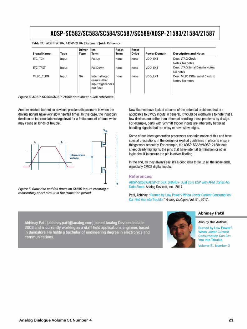
Some of our latest generation processors also take notice of this and have special precautions in the design or explicit guidelines in place to ensure things work smoothly. For example, the ADSP-SC58x/ADSP-2158x data sheet clearly highlights the pins that have internal termination or other logic circuit to ensure the pin is never floating.
In the end, as they always say, it’s a good idea to tie up all the loose ends, especially CMOS digital inputs.
References:ADSP-SC58X/ADSP-2158X: SHARC+ Dual Core DSP with ARM Cortex-A5 Data Sheet. Analog Devices, Inc., 2017.
Patil, Abhinay. “Burned by Low Power? When Lower Current Consumption Can Get You Into Trouble.” Analog Dialogue, Vol. 51, 2017.
Also by this Author:
Burned by Low Power? When Lower Current Consumption Can Get You Into Trouble
Volume 51, Number 3
Abhinay Patil [[email protected]] joined Analog Devices India in 2003 and is currently working as a staff field applications engineer, based in Bangalore. He holds a bachelor of engineering degree in electronics and communications.
Abhinay Patil
ADSP-SC582/SC583/SC584/SC587/SC589/ADSP-21583/21584/21587Table 27. ADSP-SC58x/ADSP-2158x Designer Quick Reference
Signal Name TypeDriver Type
Int Term
Reset Term
Reset Drive Power Domain Description and Notes
Figure 6. ADSP-SC58x/ADSP-2158x data sheet quick reference.

Analog Dialogue Volume 51 Number 422
Share on
When faced with rising component temperatures, the PCB designer can reach into the standard heat mitigation toolbox for commonly used tools such as additional copper, heat sinks, or bigger and faster fans, or simply more space—use more PCB real estate, increase the distance between components on the PCB, or thicken the PCB layers.
Any of these tools can be used on the PCB to maintain the system within safe temperature limits, but applying these remedies can diminish the end product’s competitive edge in the market. The product, say a router, might require a larger case to accommodate necessary component separation on the PCB, or it may become relatively noisy as faster fans are added to increase airflow. This can render the end product inferior in a market where companies compete on the merits of compactness, computational power, data rates, efficiency, and cost.
Successful thermal management around high power POL regulators requires choosing the right regulator, which demands careful research. This article shows how a regulator choice can simplify the board designer’s job.
Don’t Judge POL Regulators by Power Density AloneA number of market factors drive the need to improve thermal perfor-mance in electronic equipment. Most obvious, performance continuously improves even as products shrink in size. For instance, 28 nm to 20 nm and sub-20 nm digital devices burn power to deliver performance, as inno-vative equipment designers use these smaller processes for faster, tinier, quieter, and more efficient devices. The obvious conclusion from this trend is that POL regulators must increase in power density: (power)/(volume) or (power)/(area).
It is no surprise that power density is often cited in regulator literature as the headline specification. Impressive power densities make a regulator stand out—giving designers quotable specifications when choosing from the vast array of available regulators. A 40 W/cm2 POL regulator must be better than a 30 W/cm2 regulator.
The art of designing efficient and compact dc-to-dc converters is prac-ticed by a select group of engineers with a deep understanding of the physics and supporting mathematics involved in conversion design, com-bined with a healthy dose of bench experience. A deep understanding of Bode plots, Maxwell’s equations, and concerns for poles and zeros figure into elegant dc-to-dc converter design. Nevertheless, IC designers often avoid dealing with the dreaded topic of heat—a job that usually falls to the package engineer.
Heat is a significant concern for point-of-load (POL) converters where space is tight among delicate ICs. A POL regulator generates heat because no voltage conversion is 100% efficient (yet). How hot does the package become due to its construction, layout, and thermal impedance? Thermal impedance of the package not only raises temperature of the POL reg-ulator, it also increases the temperature of the PCB and surrounding components, contributing to the complexity, size, and cost of the system’s heat removal arrangements.
Heat mitigation for a dc-to-dc converter package on a PCB is achieved through two major strategies:
Distribute it through the PCB:If the converter IC is surface-mountable, the heat conductive copper vias and layers in the PCB disperse the heat from the bottom of the package. If the thermal impedance of the package to the PCB is low enough, this is sufficient.
Add airflow:Cool airflow removes heat from the package (or more precisely, the heat is transferred to the cooler fast air molecules in contact with the surface of the package).
Of course, there are methods of passive and active heat sinking, which, for simplicity of this discussion, are considered subsets of the second category.
How to Choose Cool Running, High Power, Scalable POL Regulators and Save Board SpaceBy Afshin Odabaee

Analog Dialogue Volume 51 Number 4 23
Product designers want to squeeze higher power into tighter spaces—superlative power density numbers appear at first blush to be the clear path to the fastest, smallest, quietest, and most efficient products, akin to comparing automobile performance using horsepower. But how significant is power density in achieving a successful final design? Less than you might think.
A POL regulator must meet the requirements of its application. In choosing a POL regulator, one must assure its ability to do the job on the PCB, where the treatment of heat can make or break the application. The following rec-ommended step-by-step selection process for a POL regulator makes the case for prioritizing thermal performance:
Ignore power density numbers:Power density specifications ignore thermal derating, which has a significantly greater effect on the effective real-world power density.
Check the regulator’s thermal derating curves:A well-documented and characterized POL regulator should have graphs specifying output current at various input voltages, output voltages, and airflow speeds. The data sheet should show the output current capability of the POL regulator under real-world operating conditions so you can judge the regulator by its thermal and load current abilities. Does it meet the requirement of your system’s typical and maximum ambient temperature and airflow speed? Remember, output current derating relates to the thermal performance of the device. The two are closely related and equally important.
Look at efficiency:Yes, efficiency is not the first consideration. Efficiency results, when used exclusively, can present an inaccurate picture of the thermal characteristics of a dc-to-dc regulator. Of course, efficiency numbers are required to calculate input current and load current, input power consumption, power dissipation, and junction temperature. Efficiency values must be combined with output current derating and other thermal data related to the device and its package.
For example, a 98% efficient, dc-to-dc step-down converter is impressive; even better when it boasts a superior power density number. Do you pur-chase it over a less efficient, less power dense regulator? A savvy engineer should ask about the effect of that seemingly insignificant 2% efficiency loss. How does that power translate into the package temperature rise during operation? What is the junction temperature of a high power den-sity, efficient regulator at 60°C ambient with 200 LFM (linear feet per minute) airflow? Look beyond the typical numbers that are listed at room temperature of 25°C. What are the maximum and minimum values that are measured at the extremes: −40°C, +85°C, or +125°C? At a high power density, does the package thermal impedance rise so high that the junction temperature shoots over the safe operating temperature? How much derating does an impressively efficient, but expensive, regulator require? Do derated output current values curtail output power capability to the point that the additional cost of the device is no longer justified?
Consider the ease of cooling the POL regulator:The package thermal impedance values provided in the data sheet are key to simulate and calculate the rise in the junction, ambient, and case temperatures of the device. Because much of the heat in surface-mount packages flows from the bottom of the package to the PCB, layout guid-ance and discussions about thermal measurements must be articulated in the data sheet to minimize surprises during system prototyping.
A well designed package should efficiently dissipate heat evenly through-out its surfaces, eliminating hot spots that degrade the reliability of a POL regulator. As described above, the PCB is responsible for absorbing and routing much of the heat from surface-mountable POL regulators. With the prevalence of forced airflow in today’s dense and complex systems, a cleverly designed POL regulator should also tap this free cooling oppor-tunity to remove heat from heat generating components such as MOSFETs and inductors.
Guiding Heat to the Top of the Package and into the AirA high power switching POL regulator depends on an inductor or transformer to convert the input supply voltage to a regulated output voltage. In a nonisolated step-down POL regulator, the device uses an inductor. The inductor and accompanying switching elements, such as MOSFETs, produce heat during dc-to-dc conversion.
About a decade ago, new packaging advances allowed an entire dc-to-dc regulator circuit, including the magnetics, to be designed and fitted inside molded plastic, called modules or SiPs, where much of the heat generated inside the molded plastic is routed to the PCB via the bottom of the pack-age. Any conventional attempt to improve the heat removal capability of the package, such as attaching a heat sink to the top of the surface-mount package, contributes to a larger package.
A few years ago, an innovative module packaging technique was devel-oped to take advantage of available airflow to aid in cooling. In this package design, a heat sink is integrated into the module package and over molded. Inside the package, the bottom of the heat sink is directly connected to the MOSFETs and inductors, while the topside of the heat sink is a flat surface exposed at the top of the package. This new intra-packaging heat sinking technique allows a device to be cooled quickly with airflow (for an example, see the LTM4620 TechClip videos here).
Go Vertical: POL Module Regulator with Stacked Inductor as Heat SinkThe size of an inductor in a POL regulator depends on voltage, switching frequency, current handling, and its construction. In a module approach where the dc-to-dc circuit, including the inductor, is overmolded and encapsulated in a plastic package and resembles an IC, the inductor dictates the thickness, volume, and weight of the package more than any other component. The inductor is also a significant source of heat.
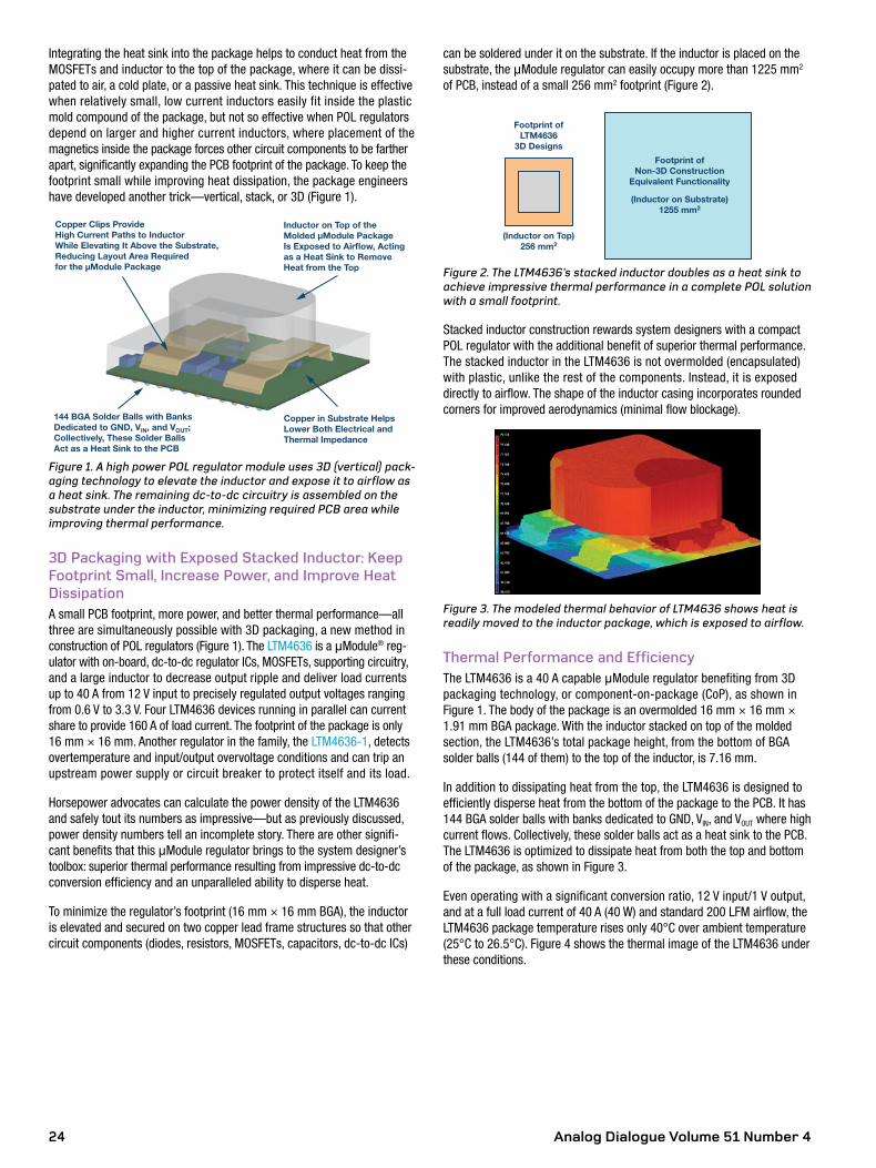
Analog Dialogue Volume 51 Number 424
Integrating the heat sink into the package helps to conduct heat from the MOSFETs and inductor to the top of the package, where it can be dissi-pated to air, a cold plate, or a passive heat sink. This technique is effective when relatively small, low current inductors easily fit inside the plastic mold compound of the package, but not so effective when POL regulators depend on larger and higher current inductors, where placement of the magnetics inside the package forces other circuit components to be farther apart, significantly expanding the PCB footprint of the package. To keep the footprint small while improving heat dissipation, the package engineers have developed another trick—vertical, stack, or 3D (Figure 1).
Copper Clips Provide High Current Paths to InductorWhile Elevating It Above the Substrate,Reducing Layout Area Requiredfor the µModule Package
144 BGA Solder Balls with BanksDedicated to GND, VIN, and VOUT;Collectively, These Solder Balls Act as a Heat Sink to the PCB
Copper in Substrate Helps Lower Both Electrical and Thermal Impedance
Inductor on Top of the Molded µModule Package Is Exposed to Airflow, Acting as a Heat Sink to Remove Heat from the Top
Figure 1. A high power POL regulator module uses 3D (vertical) pack-aging technology to elevate the inductor and expose it to airflow as a heat sink. The remaining dc-to-dc circuitry is assembled on the substrate under the inductor, minimizing required PCB area while improving thermal performance.
3D Packaging with Exposed Stacked Inductor: Keep Footprint Small, Increase Power, and Improve Heat DissipationA small PCB footprint, more power, and better thermal performance—all three are simultaneously possible with 3D packaging, a new method in construction of POL regulators (Figure 1). The LTM4636 is a µModule® reg-ulator with on-board, dc-to-dc regulator ICs, MOSFETs, supporting circuitry, and a large inductor to decrease output ripple and deliver load currents up to 40 A from 12 V input to precisely regulated output voltages ranging from 0.6 V to 3.3 V. Four LTM4636 devices running in parallel can current share to provide 160 A of load current. The footprint of the package is only 16 mm × 16 mm. Another regulator in the family, the LTM4636-1, detects overtemperature and input/output overvoltage conditions and can trip an upstream power supply or circuit breaker to protect itself and its load.
Horsepower advocates can calculate the power density of the LTM4636 and safely tout its numbers as impressive—but as previously discussed, power density numbers tell an incomplete story. There are other signifi-cant benefits that this µModule regulator brings to the system designer’s toolbox: superior thermal performance resulting from impressive dc-to-dc conversion efficiency and an unparalleled ability to disperse heat.
To minimize the regulator’s footprint (16 mm × 16 mm BGA), the inductor is elevated and secured on two copper lead frame structures so that other circuit components (diodes, resistors, MOSFETs, capacitors, dc-to-dc ICs)
can be soldered under it on the substrate. If the inductor is placed on the substrate, the µModule regulator can easily occupy more than 1225 mm2 of PCB, instead of a small 256 mm2 footprint (Figure 2).
Footprint ofNon-3D Construction
Equivalent Functionality
(Inductor on Substrate)1255 mm2
Footprint ofLTM4636
3D Designs
(Inductor on Top)256 mm2
Figure 2. The LTM4636’s stacked inductor doubles as a heat sink to achieve impressive thermal performance in a complete POL solution with a small footprint.
Stacked inductor construction rewards system designers with a compact POL regulator with the additional benefit of superior thermal performance. The stacked inductor in the LTM4636 is not overmolded (encapsulated) with plastic, unlike the rest of the components. Instead, it is exposed directly to airflow. The shape of the inductor casing incorporates rounded corners for improved aerodynamics (minimal flow blockage).
Figure 3. The modeled thermal behavior of LTM4636 shows heat is readily moved to the inductor package, which is exposed to airflow.
Thermal Performance and EfficiencyThe LTM4636 is a 40 A capable µModule regulator benefiting from 3D packaging technology, or component-on-package (CoP), as shown in Figure 1. The body of the package is an overmolded 16 mm × 16 mm × 1.91 mm BGA package. With the inductor stacked on top of the molded section, the LTM4636’s total package height, from the bottom of BGA solder balls (144 of them) to the top of the inductor, is 7.16 mm.
In addition to dissipating heat from the top, the LTM4636 is designed to efficiently disperse heat from the bottom of the package to the PCB. It has 144 BGA solder balls with banks dedicated to GND, VIN, and VOUT where high current flows. Collectively, these solder balls act as a heat sink to the PCB. The LTM4636 is optimized to dissipate heat from both the top and bottom of the package, as shown in Figure 3.
Even operating with a significant conversion ratio, 12 V input/1 V output, and at a full load current of 40 A (40 W) and standard 200 LFM airflow, the LTM4636 package temperature rises only 40°C over ambient temperature (25°C to 26.5°C). Figure 4 shows the thermal image of the LTM4636 under these conditions.
Analog Dialogue Volume 51 Number 4 25
Figure 4. Thermal results of regulator at 40 W shows a temperature rise of only 40°C.
Figure 5 shows the output current thermal derating results. At 200 LFM, the LTM4636 delivers an impressive full current of 40 A up to an 83°C ambient temperature. Half-current, 20 A derating only occurs at an excessively high ambient temperature of 110°C. This allows the LTM4636 to perform at high capacity as long as some airflow is available.
Ambient Temperature (C°)
0 20 40 60 80 100 1200
5
10
15
20
25
30
35
40
45
Load
Cur
rent
(A)
OLFM200 LFM400 LFM
Figure 5. Thermal derating shows full current of 40 A delivered up to 83°C ambient, 200 LFM.
The high conversion efficiency shown in Figure 6 is mainly a result of top performing MOSFETs and strong drivers of the LTM4636. For example, a 12 V input supply step-down dc-to-dc controller achieves:
X 95% for 12 V input to 3.3 V, 25 A X 93% for 12 V input to 1.8 V, 40 A X 88% for 12 V input to 1 V, 40 A
Output Current (A)
0 5 10 15 20 25 30 35 4070
75
80
85
90
95
100
Effi
cien
cy (%
)
VOUT = 3.3 V, fSW = 750 kHzVOUT = 2.5 V, fSW = 650 kHzVOUT = 1.8 V, fSW = 600 kHzVOUT = 1.5 V, fSW = 550 kHzVOUT = 1.2 V, fSW = 400 kHzVOUT = 1 V, fSW = 350 kHz
VIN = 12 V
Figure 6. High dc-to-dc conversion efficiency over a variety of output voltages.
140 W, Scalable 4 A × 40 A µModule POL Regulator with Thermal BalanceOne LTM4636 is rated for 40 A load current delivery. Two LTM4636s in current sharing mode (or parallel) can support 80 A, while four will support 160 A. Upscaling a power supply with parallel LTM4636s is easy; simply copy and paste the single-regulator footprint, as shown in Figure 7 (sym-bols and footprints are available).
Figure 7. It is easy to lay out parallel LTM4636s. Simply duplicate the layout of one channel.
The current mode architecture of the LTM4636 enables precision current sharing among the 40 A blocks. Precise current sharing, in turn, produces a power supply that spreads the heat evenly between devices. Figure 8 shows a 160 A regulator with four µModules. All devices with these spec-ifications operate within a °C of each other, ensuring that no individual device is overloaded or overheated. This greatly simplifies heat mitigation.
Figure 8. Precision current sharing among four LTM4636s running in parallel, resulting in only a 40°C rise in temperature for a 160 A application.
Load Current (A)
0 20 40 60 80 100 120 140 16060
70
65
75
80
85
90
95
Effi
cien
cy (%
)
Figure 9. Efficiency of a 140 W regulator with four µModules.
Analog Dialogue Volume 51 Number 426
Figure 10. This 140 W regulator features four LTM4636s running in parallel with precision current sharing and high efficiency 12 V input to 0.9 V output at 160 A.
34.8 kΩ
4.99 kΩ
7 V to 14 V
150 µF35 V
22 µF
Power GND
22 µF
22 µF
22 µF
2200 pf
2200 pf
2200 pf
2200 pf
Voltage OutTemp Monitor
Voltage OutTemp Monitor
Voltage OutTemp Monitor
Voltage OutTemp Monitor
PWM4 TP
PWM3 TP
PWM1 TP
2.2 Ω, 0805
2.2 Ω, 0805
2.2 Ω, 0805
2.2 Ω, 0805
PWM2 TP
0.47 µF
34.8 kΩ
COMP
COMP
COMP
COMP
TK/SS
TK/SS
TK/SS
TK/SS
RUNC
RUNC
RUNCRUNP
RUNP
RUNCRUNP
CLK1
CLK1
CLK2CLK3
CLK3
CLK2
RUNPINTVCC2
CSS0.47 µF
5 VPVCC1
INTVCC1
INTVCC2
U2LTM4636
U1LTM4636
U3LTM4636
U4LTM4636
INTVCC1
VOUT
COMPACOMPBTK/SS
RUNCRUNPHIZREG
PHMODEFREQMODE/PLLINCLKOUT
TEMP+TEMP– SNSP1 SNSP2 SGNDPGND
VOUT
VFB
VOUTS1–
SW
PWM
TMON
VIN INTVCC PVCC
COMPACOMPBTK/SS
RUNCRUNP
HIZREG
PHMODEFREQMODE/PLLINCLKOUT
TEMP+TEMP– SNSP1 SNSP2 SGNDPGND
VOUT
VFB
VOUTS1–
VOUTS1–
SW
PWM
TMON
VIN INTVCC PVCC
COMPACOMPBTK/SS
RUNCRUNPHIZREG
PHMODEFREQ
MODE/PLLIN
TEMP+TEMP– SNSP1 SNSP2 SGNDPGND
VOUT
VFB
SW
PWM
TMON
VIN INTVCC PVCC
COMPACOMPB
TK/SS
RUNCRUNPHIZREG
PHMODEFREQMODE/PLLINCLKOUT
TEMP+TEMP– SNSP1 SNSP2 SGNDPGND
VOUT
VFB
VOUTS1–
VOUTS1+
SW
PWM
TMON
VIN INTVCC PVCC
VFB
VFB
VFB
RFB2.5 kΩ
0.9 V at 160 A
5 V PVCC3
5 V PVCC1
5 V PVCC2
5 V PVCC4
VFB
INTVCC3
INTVCC4
INTVCC3
INTVCC4
SGND
SGND
SGND
SGND
SGND
SGND
SGND
SGND
SGND
SGND
SGND
SGND
SGND
SGND
GND_SNS
GND_SNS
GND_SNS
GND_SNS
100 pf
SGND
34.8 kΩ
12 V
Pins Not Used in Circuit U2:PGOOD, TEST1, TEST2, TEST3,TEST4, VOUTS1, GMON
Pins Not Used in Circuit U1:PGOOD, TEST1, TEST2, TEST3,TEST4, GMON
Pins Not Used in Circuit U3:PGOOD, TEST1, TEST2, TEST3,TEST4, VOUTS1, GMON
Pins Not Used in Circuit U4:PGOOD, TEST1, TEST2, TEST3,TEST4, VOUTS1, GMON
Optional Temp MonitorFor Telemetry Readback ICs
Optional Temp MonitorFor Telemetry Readback ICs
Optional Temp MonitorFor Telemetry Readback ICs
Optional Temp MonitorFor Telemetry Readback ICs
12 V
22 µF16 V
22 µF16 V
22 µF16 V
22 µF16 V
22 µF16 V
22 µF16 V
22 µF16 V
22 µF16 V
470 µF6.3 V+ +
470 µF6.3 V
100 µF6.3 V×4
470 µF6.3 V+ +
470 µF6.3 V
100 µF6.3 V×4
470 µF6.3 V+ +
470 µF6.3 V
100 µF6.3 V×4
470 µF6.3 V+ +
470 µF6.3 V
100 µF6.3 V×4
22 µF16 V
22 µF16 V
22 µF16 V
22 µF16 V
12 V
22 µF16 V
22 µF16 V
22 µF16 V
22 µF16 V
+
34.8 kΩ
Analog Dialogue Volume 51 Number 4 27
Figure 10 shows the complete 160 A design. Note that no clock device is required for the LTM4636s to operate out-of-phase respective of each other—clocking and phase control is included. Multiphase operation reduces output and input ripple current, reducing the number of required input and output capacitors. Here, the four LTM4636s in Figure 10 are running 90° out-of-phase.
ConclusionChoosing a POL regulator for a densely populated system requires scrutiny beyond the voltage and amperage ratings of the device. Evaluation of its package’s thermal characteristics is essential, as it determines the cost of cooling, cost of the PCB, and final product size. Advances in 3D, also referred to as stacked, vertical, CoP allow high power POL module regulators to fit a small PCB footprint, but, more importantly, enable efficient cooling. The LTM4636 is the first series of µModule regulators to benefit from this stacked packaging technology. As a 40 A POL µModule regulator with a stacked inductor as a heat sink, it boasts 95% to 88% efficiency, with only a 40°C rise at full load, occupying only 16 mm × 16 mm of PCB area. A video description of the LTM4636 is available at linear.com/LTM4636.
Afshin Odabaee [[email protected]] is the business development director for µModule power products and dc-to-dc controller ICs. He received his B.S. in electrical engineering with emphasis in analog from Santa Clara University in 1994. He has been working at ADI for 21 years, starting with op amps, references, and dc-to-dc regulators, and later on was assigned to help start and support the µModule power products.
Afshin Odabaee
Analog Dialogue Volume 51 Number 428
Share on
doing so, will miss critical acceleration data due to the reduced effective sampling rate. In order to measure the range of real-time human motion, power consumption has to be increased significantly. The ADXL362 and ADXL363 do not alias input signals by undersampling; they sample the full bandwidth of the sensor at all data rates. Power consumption scales dynamically with sample rate, as shown in Figure 1. Of note is the fact that these parts can sample up to 400 Hz with current consumption at only 3 µA. These higher data rates enable extra functionality in wearable device interfaces such as tap/double tap detection. The sampling rate can be reduced to 6 Hz to allow a device to start when picked up or when motion is detected, giving an average current consumption of 270 nA. This also makes the ADXL362 and ADXL363 attractive for implantable applications where batteries can’t be replaced easily.
6
5
4
3
2
1
0
Cur
rent
Co
nsum
pti
on
(μA
)
Output Data Rate (Hz)
0 100 200 300 400
VS = 1.6 VVS = 2.0 VVS = 2.5 VVS = 3.0 VVS = 3.5 V
Figure 1. ADXL362 supply current as function of the output data rate.
IntroductionChoosing the most suitable accelerometer for your application can be difficult, as data sheets from various manufacturers can differ significantly, leading to confusion as to what are the most critical specifications. In Part 2 of this article, we will focus on key specifications and features in the context of wearable devices, condition monitoring, and IoT applications.
Wearable DevicesKey criteria: Low power consumption, small size, integrated features to enhance power saving, and usability.
The key specification for accelerometers used in battery-powered, wear-able applications is ultra low power consumption, typically in the µA range, to ensure that battery life is prolonged for as long as possible. Other key criteria are size and integrated features, such as spare ADC channels and a deep FIFO to help with power management and functionality in the end application. For these reasons, MEMS accelerometers are typically used in wearable applications. Table 1 shows some vital signs monitoring (VSM) applications and their corresponding settings by context. Accelerometers used in wearable applications typically classify motion; provide freefall detection; measure the presence or absence of motion to provide system power up, down, or sleep; and help with data fusion for ECG and other VSM measurements. The same accelerometers are also used in wireless sensor networks and IoT applications due to their ultra low power consumption.
When selecting accelerometers for ultra low power applications, it is imperative to observe the functionality of the sensor at the power con-sumption levels stated in the data sheet. A key thing to observe is if the bandwidth and sample rate reduce to levels where usable acceleration data cannot be measured. Some competitor parts turn themselves off and wake up every second to maintain low power consumption and, in
Choosing the Most Suitable MEMS Accelerometer for Your Application—Part 2By Chris Murphy
Table 1. Motion Sensing Requirements for VSM Wearable Applications
Pedometer Fall Optical Heart Rate Tap (SW) Sleep Motion Switch ECG ADXL362/
ADXL363
g Setting 2 g 8 g 4 g or 8 g 8 g 2 g 2 g 4 g to 8 g 2 g to 8 g
ODR (Hz) 100 400 <50 400 12.5 6 <100 400
Power Consumption 1.8 µA 3 µA 3 µA 1.5 µA 0.3 µA 10 nA to 3 µA
FIFO (Sample Sets or Time) 150 Deeper is better 1 sec Deeper is better 20 No 1 sec 512 sec or 13 sec
ADC No No Yes No No No Yes No/yes
Noise (mg/√Hz) <1 <1 <1 <1 <1 <1 <1 175 µg to 500 µg
Data Collection 24/7 24/7 Sporadic 24/7 On motion Continuous during exercise All
Required Feature RSS, 8-bit Trigger mode FIFO Trigger mode FIFO Low noise MCU off All except RSS
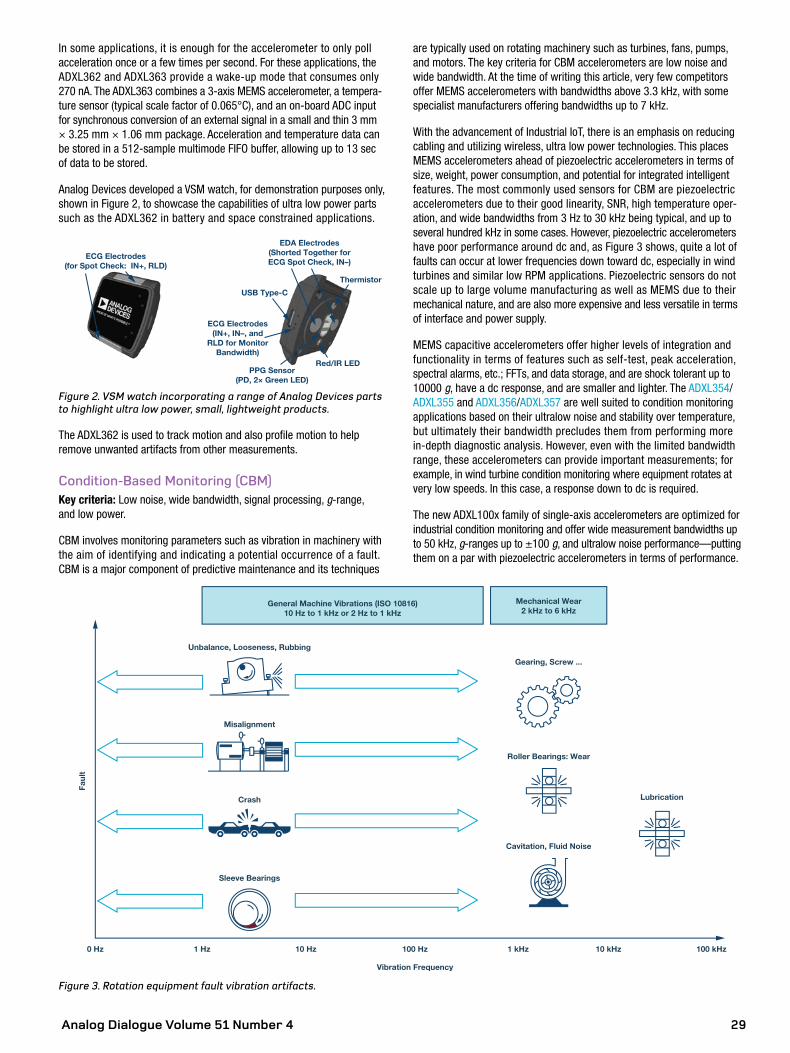
Analog Dialogue Volume 51 Number 4 29
In some applications, it is enough for the accelerometer to only poll acceleration once or a few times per second. For these applications, the ADXL362 and ADXL363 provide a wake-up mode that consumes only 270 nA. The ADXL363 combines a 3-axis MEMS accelerometer, a tempera-ture sensor (typical scale factor of 0.065°C), and an on-board ADC input for synchronous conversion of an external signal in a small and thin 3 mm × 3.25 mm × 1.06 mm package. Acceleration and temperature data can be stored in a 512-sample multimode FIFO buffer, allowing up to 13 sec of data to be stored.
Analog Devices developed a VSM watch, for demonstration purposes only, shown in Figure 2, to showcase the capabilities of ultra low power parts such as the ADXL362 in battery and space constrained applications.
ECG Electrodes(for Spot Check: IN+, RLD)
EDA Electrodes(Shorted Together for ECG Spot Check, IN–)
Red/IR LEDPPG Sensor
(PD, 2× Green LED)
ECG Electrodes(IN+, IN–, and
RLD for Monitor Bandwidth)
USB Type-C
Thermistor
Figure 2. VSM watch incorporating a range of Analog Devices parts to highlight ultra low power, small, lightweight products.
The ADXL362 is used to track motion and also profile motion to help remove unwanted artifacts from other measurements.
Condition-Based Monitoring (CBM)Key criteria: Low noise, wide bandwidth, signal processing, g-range, and low power.
CBM involves monitoring parameters such as vibration in machinery with the aim of identifying and indicating a potential occurrence of a fault. CBM is a major component of predictive maintenance and its techniques
are typically used on rotating machinery such as turbines, fans, pumps, and motors. The key criteria for CBM accelerometers are low noise and wide bandwidth. At the time of writing this article, very few competitors offer MEMS accelerometers with bandwidths above 3.3 kHz, with some specialist manufacturers offering bandwidths up to 7 kHz.
With the advancement of Industrial IoT, there is an emphasis on reducing cabling and utilizing wireless, ultra low power technologies. This places MEMS accelerometers ahead of piezoelectric accelerometers in terms of size, weight, power consumption, and potential for integrated intelligent features. The most commonly used sensors for CBM are piezoelectric accelerometers due to their good linearity, SNR, high temperature oper-ation, and wide bandwidths from 3 Hz to 30 kHz being typical, and up to several hundred kHz in some cases. However, piezoelectric accelerometers have poor performance around dc and, as Figure 3 shows, quite a lot of faults can occur at lower frequencies down toward dc, especially in wind turbines and similar low RPM applications. Piezoelectric sensors do not scale up to large volume manufacturing as well as MEMS due to their mechanical nature, and are also more expensive and less versatile in terms of interface and power supply.
MEMS capacitive accelerometers offer higher levels of integration and functionality in terms of features such as self-test, peak acceleration, spectral alarms, etc.; FFTs, and data storage, and are shock tolerant up to 10000 g, have a dc response, and are smaller and lighter. The ADXL354/ADXL355 and ADXL356/ADXL357 are well suited to condition monitoring applications based on their ultralow noise and stability over temperature, but ultimately their bandwidth precludes them from performing more in-depth diagnostic analysis. However, even with the limited bandwidth range, these accelerometers can provide important measurements; for example, in wind turbine condition monitoring where equipment rotates at very low speeds. In this case, a response down to dc is required.
The new ADXL100x family of single-axis accelerometers are optimized for industrial condition monitoring and offer wide measurement bandwidths up to 50 kHz, g-ranges up to ±100 g, and ultralow noise performance—putting them on a par with piezoelectric accelerometers in terms of performance.
1 Hz
Unbalance, Looseness, Rubbing
Gearing, Screw ...
Roller Bearings: Wear
10 Hz 100 Hz
Vibration Frequency
1 kHz 10 kHz 100 kHz0 Hz
Faul
t
Misalignment
Crash
Sleeve Bearings
Cavitation, Fluid Noise
Lubrication
Mechanical Wear2 kHz to 6 kHz
General Machine Vibrations (ISO 10816)10 Hz to 1 kHz or 2 Hz to 1 kHz
Figure 3. Rotation equipment fault vibration artifacts.
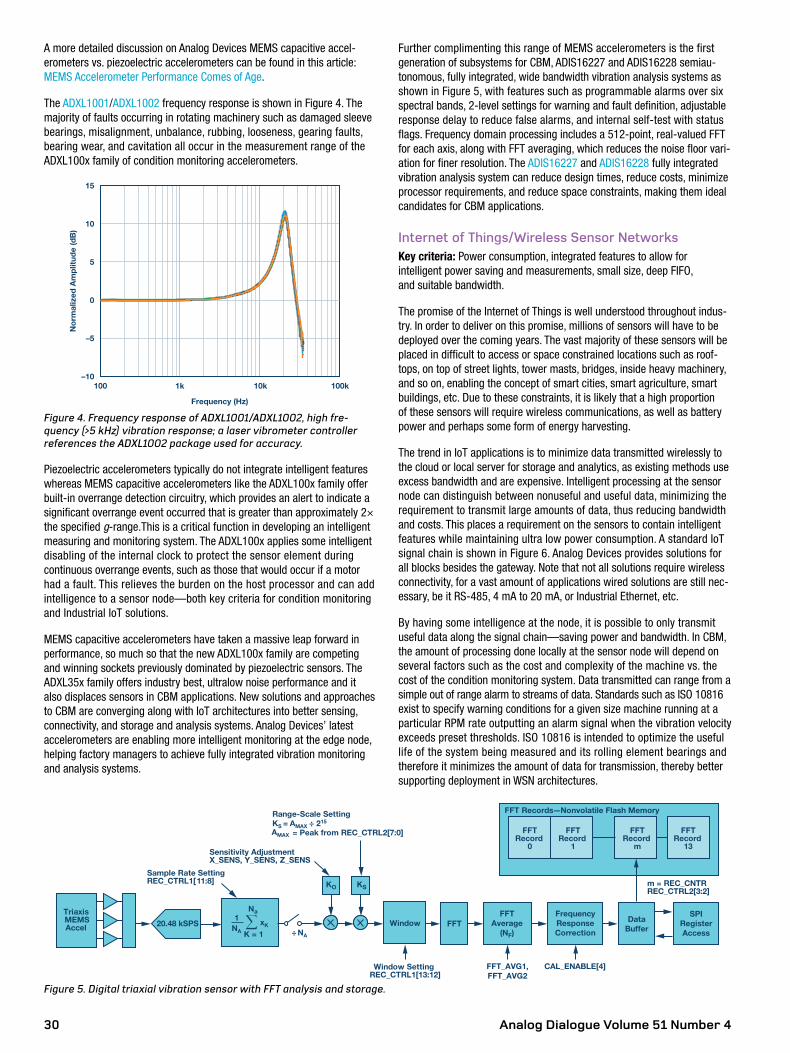
Analog Dialogue Volume 51 Number 430
A more detailed discussion on Analog Devices MEMS capacitive accel-erometers vs. piezoelectric accelerometers can be found in this article: MEMS Accelerometer Performance Comes of Age.
The ADXL1001/ADXL1002 frequency response is shown in Figure 4. The majority of faults occurring in rotating machinery such as damaged sleeve bearings, misalignment, unbalance, rubbing, looseness, gearing faults, bearing wear, and cavitation all occur in the measurement range of the ADXL100x family of condition monitoring accelerometers.
–10
–5
0
5
10
15
100 1k 10k 100k
No
rmal
ized
Am
plit
ude
(dB
)
Frequency (Hz)
Figure 4. Frequency response of ADXL1001/ADXL1002, high fre-quency (>5 kHz) vibration response; a laser vibrometer controller references the ADXL1002 package used for accuracy.
Piezoelectric accelerometers typically do not integrate intelligent features whereas MEMS capacitive accelerometers like the ADXL100x family offer built-in overrange detection circuitry, which provides an alert to indicate a significant overrange event occurred that is greater than approximately 2× the specified g-range.This is a critical function in developing an intelligent measuring and monitoring system. The ADXL100x applies some intelligent disabling of the internal clock to protect the sensor element during continuous overrange events, such as those that would occur if a motor had a fault. This relieves the burden on the host processor and can add intelligence to a sensor node—both key criteria for condition monitoring and Industrial IoT solutions.
MEMS capacitive accelerometers have taken a massive leap forward in performance, so much so that the new ADXL100x family are competing and winning sockets previously dominated by piezoelectric sensors. The ADXL35x family offers industry best, ultralow noise performance and it also displaces sensors in CBM applications. New solutions and approaches to CBM are converging along with IoT architectures into better sensing, connectivity, and storage and analysis systems. Analog Devices’ latest accelerometers are enabling more intelligent monitoring at the edge node, helping factory managers to achieve fully integrated vibration monitoring and analysis systems.
Further complimenting this range of MEMS accelerometers is the first generation of subsystems for CBM, ADIS16227 and ADIS16228 semiau-tonomous, fully integrated, wide bandwidth vibration analysis systems as shown in Figure 5, with features such as programmable alarms over six spectral bands, 2-level settings for warning and fault definition, adjustable response delay to reduce false alarms, and internal self-test with status flags. Frequency domain processing includes a 512-point, real-valued FFT for each axis, along with FFT averaging, which reduces the noise floor vari-ation for finer resolution. The ADIS16227 and ADIS16228 fully integrated vibration analysis system can reduce design times, reduce costs, minimize processor requirements, and reduce space constraints, making them ideal candidates for CBM applications.
Internet of Things/Wireless Sensor NetworksKey criteria: Power consumption, integrated features to allow for intelligent power saving and measurements, small size, deep FIFO, and suitable bandwidth.
The promise of the Internet of Things is well understood throughout indus-try. In order to deliver on this promise, millions of sensors will have to be deployed over the coming years. The vast majority of these sensors will be placed in difficult to access or space constrained locations such as roof-tops, on top of street lights, tower masts, bridges, inside heavy machinery, and so on, enabling the concept of smart cities, smart agriculture, smart buildings, etc. Due to these constraints, it is likely that a high proportion of these sensors will require wireless communications, as well as battery power and perhaps some form of energy harvesting.
The trend in IoT applications is to minimize data transmitted wirelessly to the cloud or local server for storage and analytics, as existing methods use excess bandwidth and are expensive. Intelligent processing at the sensor node can distinguish between nonuseful and useful data, minimizing the requirement to transmit large amounts of data, thus reducing bandwidth and costs. This places a requirement on the sensors to contain intelligent features while maintaining ultra low power consumption. A standard IoT signal chain is shown in Figure 6. Analog Devices provides solutions for all blocks besides the gateway. Note that not all solutions require wireless connectivity, for a vast amount of applications wired solutions are still nec-essary, be it RS-485, 4 mA to 20 mA, or Industrial Ethernet, etc.
By having some intelligence at the node, it is possible to only transmit useful data along the signal chain—saving power and bandwidth. In CBM, the amount of processing done locally at the sensor node will depend on several factors such as the cost and complexity of the machine vs. the cost of the condition monitoring system. Data transmitted can range from a simple out of range alarm to streams of data. Standards such as ISO 10816 exist to specify warning conditions for a given size machine running at a particular RPM rate outputting an alarm signal when the vibration velocity exceeds preset thresholds. ISO 10816 is intended to optimize the useful life of the system being measured and its rolling element bearings and therefore it minimizes the amount of data for transmission, thereby better supporting deployment in WSN architectures.
K = 1xKNA
Na1
÷ NA
TriaxisMEMSAccel 20.48 kSPS
KO KS
FFT
FFT_AVG1,FFT_AVG2
CAL_ENABLE[4]
FFTAverage
(NF)
FFTRecord
m
Sample Rate SettingREC_CTRL1[11:8]
Window SettingREC_CTRL1[13:12]
Range-Scale SettingKS = AMAX
AMAX
÷ 215
= Peak from REC_CTRL2[7:0] FFTRecord
0
FFT Records—Nonvolatile Flash Memory
m = REC_CNTRREC_CTRL2[3:2]
Window DataBuffer
FrequencyResponseCorrection
SPIRegisterAccess
Sensitivity AdjustmentX_SENS, Y_SENS, Z_SENS
FFTRecord
13
FFTRecord
1
Figure 5. Digital triaxial vibration sensor with FFT analysis and storage.
Analog Dialogue Volume 51 Number 4 31
The requirements for an accelerometer used in an ISO 10816 application are a g-range of 50 g or less and low noise at low frequencies as acceleration data is periodically integrated to get a single velocity point in mm/sec rms. When accelerometer data containing low frequency noise is integrated, the error can increase linearly in the velocity output. ISO standards specify a 1 Hz to 1 kHz measurement range, but users would like to integrate as low as 0.1 Hz. Traditionally, this has been limited by the high levels of noise at low frequencies in charge coupled piezoelectric accelerometers, but Analog Devices next-generation accelerometers maintain the noise floor down to dc, limited only by the 1/f noise corner of the signal conditioning electronics that can be minimized to 0.01 Hz with careful design. MEMS accelerometers can be used in economical CBM applications for lower cost equipment or can be integrated into embedded solutions due to their smaller size and lower cost compared to piezoelectric sensors.
Analog Devices have a wide range of accelerometers that are ideal for use in intelligent sensor nodes that require ultra low power, including as many features as possible to prolong battery life and help reduce bandwidth usage and thus costs. Some of the key criteria for IoT sensor nodes are low power consumption (ADXL362, ADXL363), and having a rich feature set to allow energy management and detection of specific data such as over threshold activity, spectral profile alarms, peak acceleration values, and prolonged activity or inactivity (ADXL372, ADXL375).
All of these accelerometers can keep the entire system powered off while storing acceleration data in the FIFO and looking for an activity event. When the impact event occurs, data that was collected prior to the event is frozen in the FIFO. Without a FIFO, capturing samples prior to an event would require continuous sampling and processing of acceleration signals by the processor, which significantly decreases battery life. The ADXL362 and ADXL363 FIFO can store over 13 sec of data, providing a clear picture of events prior to an activity trigger. Ultra low power consumption is maintained by not utilizing power duty cycling, but rather employing a full bandwidth architecture at all data rates, which prevents aliasing of input signals.
Asset Health MonitoringKey criteria: Power consumption, integrated features to allow for intelligent power saving and measurements, small size, deep FIFO, and suitable bandwidth.
Asset health monitoring (AHM) typically involves monitoring of a high value asset over a period of time, whether it be static or in transit. These assets could be goods inside shipping containers, remote pipelines, civilians, sol-diers, high density batteries, etc., that are susceptible to impact or shock events. The Internet of Things provides an ideal infrastructure for reporting such events that could affect an asset’s function or safety. The key criteria for a sensor used for AHM is the ability to measure high g shock, relevant to the asset, and impact events while consuming very low power. When embedding such sensors in battery operated or portable applications, other key sensor specifications to consider include size, oversampling, and antialiasing features to accurately process high frequency content, as well as intelligent features to extend battery life by maximizing host processor sleep time, and allowing interrupt driven algorithms for detecting and cap-turing shock profiles.
The ADXL372 micropower, ±200 g MEMS accelerometer targets the emerging asset health market space for intelligent IoT edge nodes. This part contains several unique features developed specifically for the AHM market to simplify the system design and provide system-level power savings. High g events such as shock or impact are often closely asso-ciated with acceleration content over a wide range of frequencies. Wide bandwidth is required to accurately capture these events, as measuring with insufficient bandwidth will effectively reduce the magnitude of the recorded event, leading to inaccuracies. This is a key parameter to observe in data sheets. Some parts don’t satisfy the Nyquist criteria for sampling rates. The ADXL375 and ADXL372 provide the option of capturing the entire shock profile for further analysis with no intervention from a host proces-sor. This is achieved using the shock interrupt registers in combination with the accelerometer’s internal FIFO. Figure 7 shows the importance of having a sufficient FIFO in order to determine the entire shock profile prior to the trigger event. With an insufficient FIFO, it would not be possible to record and maintain the shock event for further analysis.
Sense Measure Interpret Connect Analyze
RS-485/ Ethernet
RS-485/ Ethernet
Wireless Solution
Wired Solution
Power Power Power Power
Accelerometer Signal
Processing
Tx Rx
Power Power
Power Power
ADIS162xx, ADIS64xx
Energy Harvesting
ADXL100x, ADXL354/ADXL356, ADXL377
ADXL355/ADXL357, ADXL36x, ADXL37x
ADC
Figure 6. Edge sensor node solutions provided by Analog Devices.
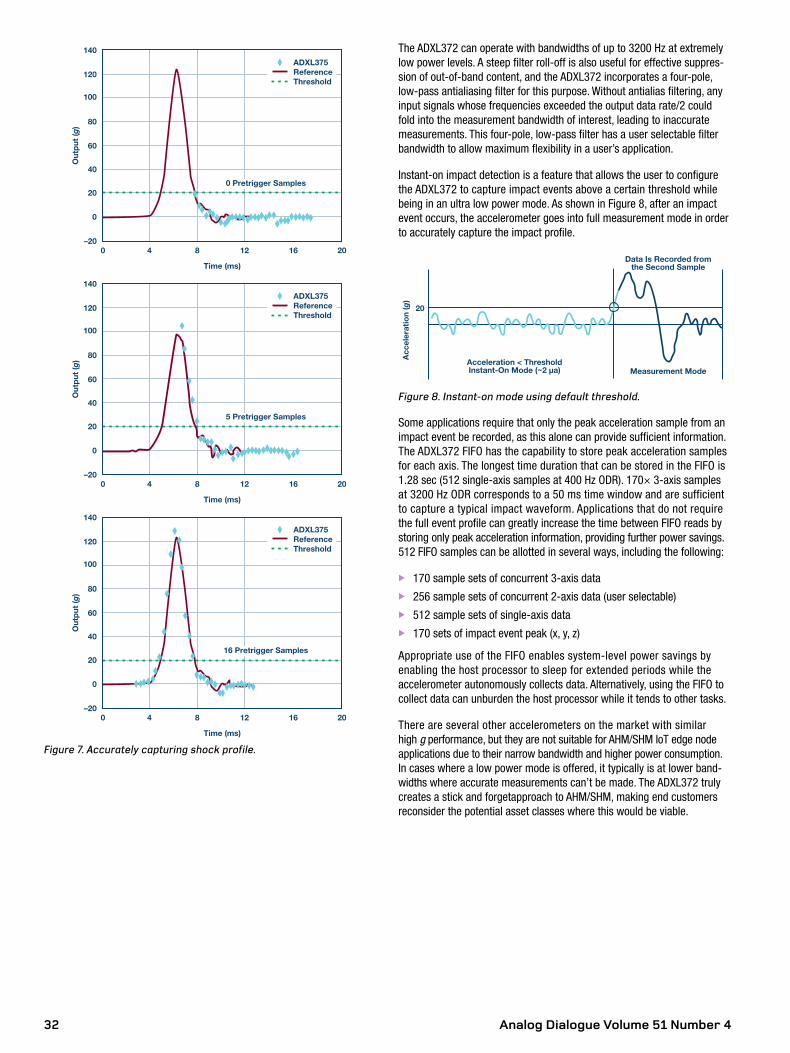
Analog Dialogue Volume 51 Number 432
–20
60
40
20
0
80
100
120
140
0 4 8 12 16 20
Out
put
(g)
Time (ms)
0 Pretrigger Samples
ADXL375ReferenceThreshold
–20
60
40
20
0
80
100
120
140
0 4 8 12 16 20
Out
put
(g)
Time (ms)
5 Pretrigger Samples
ADXL375ReferenceThreshold
–20
60
40
20
0
80
100
120
140
0 4 8 12 16 20
Out
put
(g)
Time (ms)
16 Pretrigger Samples
ADXL375ReferenceThreshold
Figure 7. Accurately capturing shock profile.
The ADXL372 can operate with bandwidths of up to 3200 Hz at extremely low power levels. A steep filter roll-off is also useful for effective suppres-sion of out-of-band content, and the ADXL372 incorporates a four-pole, low-pass antialiasing filter for this purpose. Without antialias filtering, any input signals whose frequencies exceeded the output data rate/2 could fold into the measurement bandwidth of interest, leading to inaccurate measurements. This four-pole, low-pass filter has a user selectable filter bandwidth to allow maximum flexibility in a user’s application.
Instant-on impact detection is a feature that allows the user to configure the ADXL372 to capture impact events above a certain threshold while being in an ultra low power mode. As shown in Figure 8, after an impact event occurs, the accelerometer goes into full measurement mode in order to accurately capture the impact profile.
Acceleration < ThresholdInstant-On Mode (~2 µa)
Data Is Recorded fromthe Second Sample
Measurement Mode
20
Acce
lera
tion
(g)
Figure 8. Instant-on mode using default threshold.
Some applications require that only the peak acceleration sample from an impact event be recorded, as this alone can provide sufficient information. The ADXL372 FIFO has the capability to store peak acceleration samples for each axis. The longest time duration that can be stored in the FIFO is 1.28 sec (512 single-axis samples at 400 Hz ODR). 170× 3-axis samples at 3200 Hz ODR corresponds to a 50 ms time window and are sufficient to capture a typical impact waveform. Applications that do not require the full event profile can greatly increase the time between FIFO reads by storing only peak acceleration information, providing further power savings. 512 FIFO samples can be allotted in several ways, including the following:
X 170 sample sets of concurrent 3-axis data X 256 sample sets of concurrent 2-axis data (user selectable) X 512 sample sets of single-axis data X 170 sets of impact event peak (x, y, z)
Appropriate use of the FIFO enables system-level power savings by enabling the host processor to sleep for extended periods while the accelerometer autonomously collects data. Alternatively, using the FIFO to collect data can unburden the host processor while it tends to other tasks.
There are several other accelerometers on the market with similar high g performance, but they are not suitable for AHM/SHM IoT edge node applications due to their narrow bandwidth and higher power consumption. In cases where a low power mode is offered, it typically is at lower band-widths where accurate measurements can’t be made. The ADXL372 truly creates a stick and forgetapproach to AHM/SHM, making end customers reconsider the potential asset classes where this would be viable.
Analog Dialogue Volume 51 Number 4 33
ConclusionAnalog Devices provides an extremely broad range of accelerometers to suit a multitude of applications, some of which were not focused on in this article, like dead reckoning, AHRS, inertial measurements, automotive stabilization and safety, and medical alignment. Our next-generation MEMS capacitive accelerometers are ideally suited to applications demanding low noise, low power, high stability, and performance over temperature; minimal compensation; and integrated intelligent features to improve overall system performance and ease design complexity. Analog Devices provides all the relevant data sheet information to help you choose the most suitable part for your application. All of the devices listed above, and more, are readily available for evaluation and prototyping. Visit analog.com/MEMS for more details.
ReferencesBroeders, Jan-Hein. “Transition from Wearable to Medical Devices.” Analog Devices, Inc., 2017.
Scannel, Bob. “Embedded Intelligence and Communication Enabling Reliable and Continuous Vibration Monitoring.” Analog Devices, Inc., 2015.
Spence, Ed. “What You Need to Know About MEMS Accelerometers for Condition Monitoring.” Analog Devices, Inc., 2016.
Chris Murphy [[email protected]] is an applications engineer with the European Centralized Applications Center, based in Dublin, Ireland. He has worked for Analog Devices since 2012, providing design support on motor control and industrial automation products. He holds a master’s of engineering in electronics by research and a bachelor’s of engineering in computer engineering.
Chris Murphy
Also by this Author:
Choosing the Most Suitable MEMS Accelerometer for Your Application—Part 1
Volume 51, Number 4
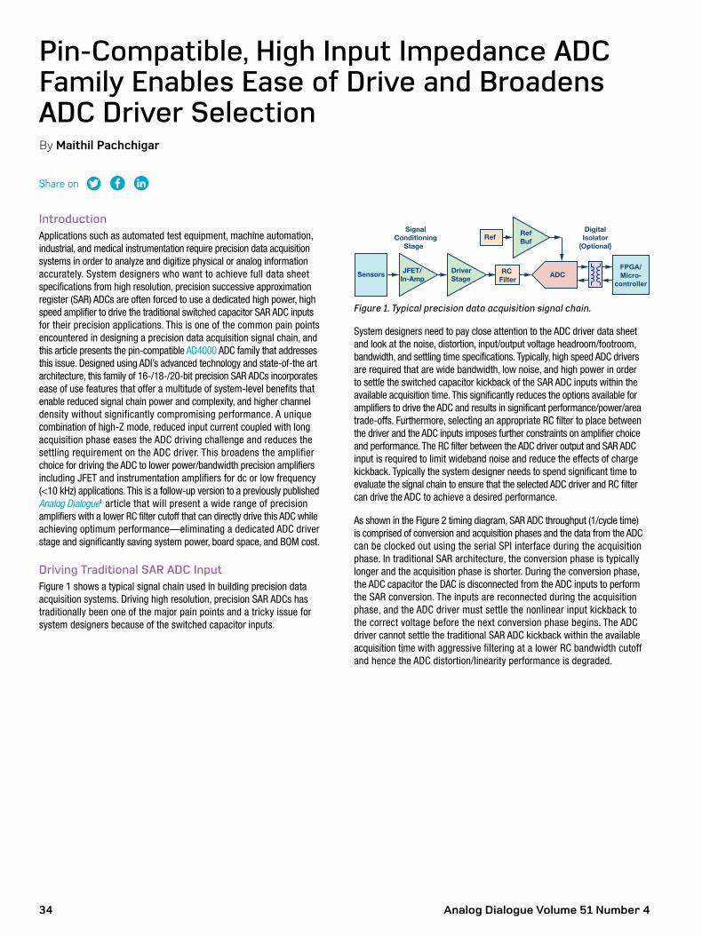
Analog Dialogue Volume 51 Number 434
Share on
SignalConditioning
Stage
Sensors RC Filter
DriverStage ADC
Ref
FPGA/Micro-
controller
RefBuf
DigitalIsolator
(Optional)
JFET/In-Amp
Figure 1. Typical precision data acquisition signal chain.
System designers need to pay close attention to the ADC driver data sheet and look at the noise, distortion, input/output voltage headroom/footroom, bandwidth, and settling time specifications. Typically, high speed ADC drivers are required that are wide bandwidth, low noise, and high power in order to settle the switched capacitor kickback of the SAR ADC inputs within the available acquisition time. This significantly reduces the options available for amplifiers to drive the ADC and results in significant performance/power/area trade-offs. Furthermore, selecting an appropriate RC filter to place between the driver and the ADC inputs imposes further constraints on amplifier choice and performance. The RC filter between the ADC driver output and SAR ADC input is required to limit wideband noise and reduce the effects of charge kickback. Typically the system designer needs to spend significant time to evaluate the signal chain to ensure that the selected ADC driver and RC filter can drive the ADC to achieve a desired performance.
As shown in the Figure 2 timing diagram, SAR ADC throughput (1/cycle time) is comprised of conversion and acquisition phases and the data from the ADC can be clocked out using the serial SPI interface during the acquisition phase. In traditional SAR architecture, the conversion phase is typically longer and the acquisition phase is shorter. During the conversion phase, the ADC capacitor the DAC is disconnected from the ADC inputs to perform the SAR conversion. The inputs are reconnected during the acquisition phase, and the ADC driver must settle the nonlinear input kickback to the correct voltage before the next conversion phase begins. The ADC driver cannot settle the traditional SAR ADC kickback within the available acquisition time with aggressive filtering at a lower RC bandwidth cutoff and hence the ADC distortion/linearity performance is degraded.
IntroductionApplications such as automated test equipment, machine automation, industrial, and medical instrumentation require precision data acquisition systems in order to analyze and digitize physical or analog information accurately. System designers who want to achieve full data sheet specifications from high resolution, precision successive approximation register (SAR) ADCs are often forced to use a dedicated high power, high speed amplifier to drive the traditional switched capacitor SAR ADC inputs for their precision applications. This is one of the common pain points encountered in designing a precision data acquisition signal chain, and this article presents the pin-compatible AD4000 ADC family that addresses this issue. Designed using ADI’s advanced technology and state-of-the art architecture, this family of 16-/18-/20-bit precision SAR ADCs incorporates ease of use features that offer a multitude of system-level benefits that enable reduced signal chain power and complexity, and higher channel density without significantly compromising performance. A unique combination of high-Z mode, reduced input current coupled with long acquisition phase eases the ADC driving challenge and reduces the settling requirement on the ADC driver. This broadens the amplifier choice for driving the ADC to lower power/bandwidth precision amplifiers including JFET and instrumentation amplifiers for dc or low frequency (<10 kHz) applications. This is a follow-up version to a previously published Analog Dialogue1 article that will present a wide range of precision amplifiers with a lower RC filter cutoff that can directly drive this ADC while achieving optimum performance—eliminating a dedicated ADC driver stage and significantly saving system power, board space, and BOM cost.
Driving Traditional SAR ADC InputFigure 1 shows a typical signal chain used in building precision data acquisition systems. Driving high resolution, precision SAR ADCs has traditionally been one of the major pain points and a tricky issue for system designers because of the switched capacitor inputs.
Pin-Compatible, High Input Impedance ADC Family Enables Ease of Drive and Broadens ADC Driver Selection By Maithil Pachchigar
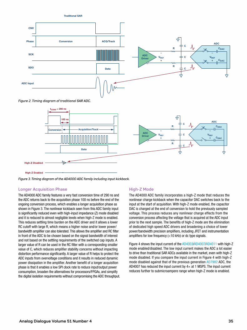
Analog Dialogue Volume 51 Number 4 35
Figure 2. Timing diagram of traditional SAR ADC.
Figure 3. Timing diagram of the AD4000 ADC family including input kickback.
Conversion Acquisition/Track
Data
High-Z Enabled
High-Z Disabled
tCONV = 290 ns
100 ns
CDACC
C
R
RC
ADC
CDACVREF
ADCDriver VREF
–
+
–
+
Traditional SAR
Conversion ACQ/TrackPhase
CNV
SCK
SDO Data
ADC Input
CDACC
C
R
RC
ADC
CDACVREF
ADCDriver VREF
–
+
–
+
Longer Acquisition PhaseThe AD4000 ADC family features a very fast conversion time of 290 ns and the ADC returns back to the acquisition phase 100 ns before the end of the ongoing conversion process, which enables a longer acquisition phase as shown in Figure 3. The nonlinear kickback seen from this ADC family input is significantly reduced even with high-input impedance (Z) mode disabled and it is reduced to almost negligible levels when high-Z mode is enabled. This reduces settling time burden on the ADC driver and it allows a lower RC cutoff with large R, which means a higher noise and/or lower power/bandwidth amplifier can also tolerated. This allows the amplifier and RC filter in front of the ADC to be chosen based on the signal bandwidth of interest and not based on the settling requirements of the switched cap inputs. A larger value of R can be used in the RC filter with a corresponding smaller value of C, which reduces amplifier stability concerns without impacting distortion performance significantly. A larger value of R helps to protect the ADC inputs from overvoltage conditions and it results in reduced dynamic power dissipation in the amplifier. Another benefit of a longer acquisition phase is that it enables a low SPI clock rate to reduce input/output power consumption, broaden the alternatives for processors/FPGAs, and simplify the digital isolation requirements without compromising the ADC throughput.
High-Z ModeThe AD4000 ADC family incorporates a high-Z mode that reduces the nonlinear charge kickback when the capacitor DAC switches back to the input at the start of acquisition. With high-Z mode enabled, the capacitor DAC is charged at the end of conversion to hold the previously sampled voltage. This process reduces any nonlinear charge effects from the conversion process affecting the voltage that is acquired at the ADC input prior to the next sample. The benefits of high-Z mode are the elimination of dedicated high speed ADC drivers and broadening a choice of lower power/bandwidth precision amplifiers, including JFET and instrumentation amplifiers for low frequency (<10 kHz) or dc type signals.
Figure 4 shows the input current of the AD4003/AD4007/AD4011 with high-Z mode enabled/disabled. The low input current makes the ADC a lot easier to drive than traditional SAR ADCs available in the market, even with high-Z mode disabled. If you compare the input current in Figure 4 with high-Z mode disabled against that of the previous generation AD7982 ADC, the AD4007 has reduced the input current by 4× at 1 MSPS. The input current reduces further to submicroampere range when high-Z mode is enabled.
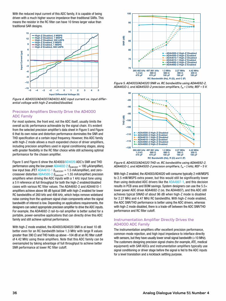
Analog Dialogue Volume 51 Number 436
With the reduced input current of this ADC family, it is capable of being driven with a much higher source impedance than traditional SARs. This means the resistor in the RC filter can have 10 times larger value than traditional SAR designs.
–15
–12
–9
–6
–3
0
3
6
9
12
15
–5 –4 –3 –2 –1 0 1 2 3 4 5
Inp
ut C
urre
nt (µ
a)
Input Differential Voltage (V)
High-Z Disabled, 2 MSPSHigh-Z Disabled, 1 MSPSHigh-Z Disabled, 500 kSPSHigh-Z Enabled, 2 MSPSHigh-Z Enabled, 1 MSPSHigh-Z Enabled, 500 kSPS
Figure 4. AD4003/AD4007/AD4011 ADC input current vs. input differ-ential voltage with high-Z enabled/disabled.
Precision Amplifiers Directly Drive the AD4000 ADC FamilyFor most systems, the front end, not the ADC itself, usually limits the overall ac/dc performance achievable by the signal chain. It’s evident from the selected precision amplifier’s data sheet in Figure 5 and Figure 6 that its own noise and distortion performance dominates the SNR and THD specification at a certain input frequency. However, this ADC family with high-Z mode allows a much expanded choice of driver amplifiers, including precision amplifiers used in signal conditioning stages, along with greater flexibility in the RC filter choice while still achieving optimal performance for the chosen amplifier.
Figure 5 and Figure 6 show the AD4003/AD4020 ADC’s SNR and THD performance using the low power ADA4692-2 (IQUIESCENT = 180 μA/amplifier), low input bias JFET ADA4610-1 (IQUIESCENT = 1.5 mA/amplifier), and zero-crossover distortion ADA4500-2 (IQUIESCENT = 1.55 mA/amplifier) precision amplifiers when driving the ADC inputs with a 1 kHz input tone using a 5 V reference at full throughput for both the high-Z enabled/disabled cases with various RC filter values. The ADA4692-2 and ADA4610-1 amplifiers achieve above 98 dB typical SNR with high-Z enabled for lower RC bandwidths of 260 kHz and 498 kHz, which helps remove wideband noise coming from the upstream signal chain components when the signal bandwidth of interest is low. Depending on applications requirements, the designers can select appropriate precision amplifier to drive the ADC inputs. For example, the ADA4692-2 rail-to-rail amplifier is better suited for a portable, power-sensitive applications that can directly drive this ADC family and still achieve optimal performance.
With high-Z mode enabled, the AD4003/AD4020 SNR is at least 10 dB better even for an RC bandwidth below 1.3 MHz with large R values greater than 390 Ω and THD holds up above –104 dB at an RC filter cutoff of 4.42 MHz using these amplifiers. Note that this ADC family can be oversampled by taking advantage of full throughput to achieve better SNR performance at lower RC filter cutoff.
70
75
80
85
90
95
100
260.482 kHz1.3 kΩ470 pF
497.981 kHz 680 Ω470 pF
1.3 MHz680 Ω180 pF
2.27 MHz390 Ω180 pF
4.42 MHz200 Ω180 pF
SN
R (d
B)
RC Bandwidth (Hz), R (Ω), and C (F)
ADA4500-2 High-Z DisabledADA4500-2 High-Z EnabledADA4610-1 High-Z DisabledADA4610-1 High-Z EnabledADA4692-2 High-Z DisabledADA4692-2 High-Z Enabled
Figure 5. AD4003/AD4020 SNR vs. RC bandwidths using ADA4692-2, ADA4610-1, and ADA4500-2 precision amplifiers, fIN = 1 kHz, REF = 5 V.
–120
–115
–110
–105
–100
–95
–90
–85
80
260.482 kHz1.3 kΩ470 pF
497.981 kHz 680 Ω470 pF
1.3 MHz680 Ω180 pF
2.27 MHz390 Ω180 pF
4.42 MHz200 Ω180 pF
TH
D (d
B)
RC Bandwidth (Hz), R (Ω) and C (F)
ADA4500-2 High-Z DisabledADA4500-2 High-Z EnabledADA4610-1 High-Z DisabledADA4610-1 High-Z EnabledADA4692-2 High-Z DisabledADA4692-2 High-Z Enabled
Figure 6. AD4003/AD4020 THD vs. RC bandwidths using ADA4692-2, ADA4610-1, and ADA4500-2 precision amplifiers, fIN = 1 kHz, REF = 5 V.
With high-Z enabled, the AD4003/AD4020 will consume typically 2 mW/MSPS to 2.5 mW/MSPS extra power, but this would still be significantly lower than using dedicated ADC drivers like the ADA4807-1, and this decision results in PCB area and BOM savings. System designers can use the 5.5× lower power ADC driver ADA4692-2 (vs. the ADA4807), and this ADC still achieves typical SINAD of about 96 dB when high-Z mode is disabled for 2.27 MHz and 4.47 MHz RC bandwidths. With high-Z mode enabled, the ADC SNR/THD performance is better using the ADC drivers, whereas with high-Z mode disabled, there is a trade-off between the ADC SNR/THD performance and RC filter cutoff.
Instrumentation Amplifier Directly Drives the AD4000 ADC FamilyThe instrumentation amplifiers offer excellent precision performance, common-mode rejection, and high input impedance to interface directly with sensors, but they have usually lower small signal bandwidth (<10 MHz). The customers designing precision signal chains (for example, ATE, medical equipment) with SAR ADCs and instrumentation amplifiers typically use signal conditioning or driver stage before the signal is fed to the ADC inputs for a level translation and a kickback settling purpose.
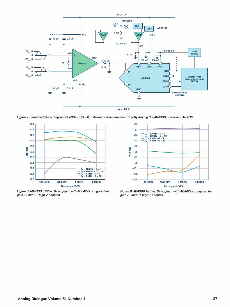
Analog Dialogue Volume 51 Number 4 37
25 nF REF VDD VIO
GND
IN+
+IN
IN–
–IN
SDI
SCK
SDO
CNV
AD4000
ADA4850
ADR4550
REF
1.8 V
1.8 V to 5 V
ADP7118
+VS = 7 V
+VS
–VS
RG
–VS = –2.5 V
Digital Host(Microprocessor/
FPGA)
HostSupply
100 nF 100 nF
5 V
2.5 V
VREF
/4
–VREF
/4
0
VREF
/4
–VREF
/4
0
REF1
LDO
AMPAMP
10 µF
0.1 µF
1 kΩ
1 kΩ
600 Ω
10 µF
0.1 µF10 µF
3-Wire/4-WireInterface
AD8422
88.0
88.5
89.0
89.5
90.0
90.5
91.0
91.5
92.0
92.5
93.0
100 kSPS 500 kSPS 1 MSPS 2 MSPS
SN
R (d
B)
Throughput (SPS)
fIN – 100 Hz – G = 1fIN – 100 Hz – G = 10fIN – 1 kHz – G = 1fIN – 1 kHz – G = 10
–105
–103
–101
–99
–97
–95
–93
–91
–89
–87
–85
100 kSPS 500 kSPS 1 MSPS 2 MSPS
TH
D (d
B)
Throughput (SPS)
fIN – 100 Hz – G = 1fIN – 100 Hz – G = 10fIN – 1 kHz – G = 1fIN – 1 kHz – G = 10
Figure 7. Simplified block diagram of AD8422 (G = 1) instrumentation amplifier directly driving the AD4000 precision SAR ADC.
Figure 8. AD4000 SNR vs. throughput with AD8422 configured for gain = 1 and 10, high-Z enabled.
Figure 9. AD4000 THD vs. throughput with AD8422 configured for gain = 1 and 10, high-Z enabled.
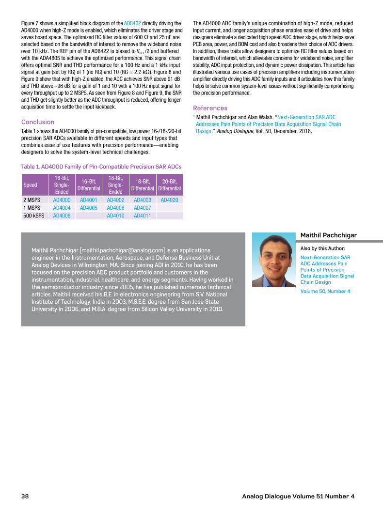
Analog Dialogue Volume 51 Number 438
Figure 7 shows a simplified block diagram of the AD8422 directly driving the AD4000 when high-Z mode is enabled, which eliminates the driver stage and saves board space. The optimized RC filter values of 600 Ω and 25 nF are selected based on the bandwidth of interest to remove the wideband noise over 10 kHz. The REF pin of the AD8422 is biased to VREF/2 and buffered with the ADA4805 to achieve the optimized performance. This signal chain offers optimal SNR and THD performance for a 100 Hz and a 1 kHz input signal at gain (set by RG) of 1 (no RG) and 10 (RG = 2.2 kΩ). Figure 8 and Figure 9 show that with high-Z enabled, the ADC achieves SNR above 91 dB and THD above –96 dB for a gain of 1 and 10 with a 100 Hz input signal for every throughput up to 2 MSPS. As seen from Figure 8 and Figure 9, the SNR and THD get slightly better as the ADC throughput is reduced, offering longer acquisition time to settle the input kickback.
ConclusionTable 1 shows the AD4000 family of pin-compatible, low power 16-/18-/20-bit precision SAR ADCs available in different speeds and input types that combines ease of use features with precision performance—enabling designers to solve the system-level technical challenges.
Table 1. AD4000 Family of Pin-Compatible Precision SAR ADCs
Speed16-Bit, Single-Ended
16-Bit, Differential
18-Bit, Single-Ended
18-Bit, Differential
20-Bit, Differential
2 MSPS AD4000 AD4001 AD4002 AD4003 AD40201 MSPS AD4004 AD4005 AD4006 AD4007500 kSPS AD4008 AD4010 AD4011
The AD4000 ADC family’s unique combination of high-Z mode, reduced input current, and longer acquisition phase enables ease of drive and helps designers eliminate a dedicated high speed ADC driver stage, which helps save PCB area, power, and BOM cost and also broadens their choice of ADC drivers. In addition, these traits allow designers to optimize RC filter values based on bandwidth of interest, which alleviates concerns for wideband noise, amplifier stability, ADC input protection, and dynamic power dissipation. This article has illustrated various use cases of precision amplifiers including instrumentation amplifier directly driving this ADC family inputs and it articulates how this family helps to solve common system-level issues without significantly compromising the precision performance.
References 1 Mathil Pachchigar and Alan Walsh. “Next-Generation SAR ADC
Addresses Pain Points of Precision Data Acquisition Signal Chain Design.” Analog Dialogue, Vol. 50, December, 2016.
Maithil Pachchigar [[email protected]] is an applications engineer in the Instrumentation, Aerospace, and Defense Business Unit at Analog Devices in Wilmington, MA. Since joining ADI in 2010, he has been focused on the precision ADC product portfolio and customers in the instrumentation, industrial, healthcare, and energy segments. Having worked in the semiconductor industry since 2005, he has published numerous technical articles. Maithil received his B.E. in electronics engineering from S.V. National Institute of Technology, India in 2003, M.S.E.E. degree from San Jose State University in 2006, and M.B.A. degree from Silicon Valley University in 2010.
Maithil Pachchigar
Also by this Author:
Next-Generation SAR ADC Addresses Pain Points of Precision Data Acquisition Signal Chain Design
Volume 50, Number 4
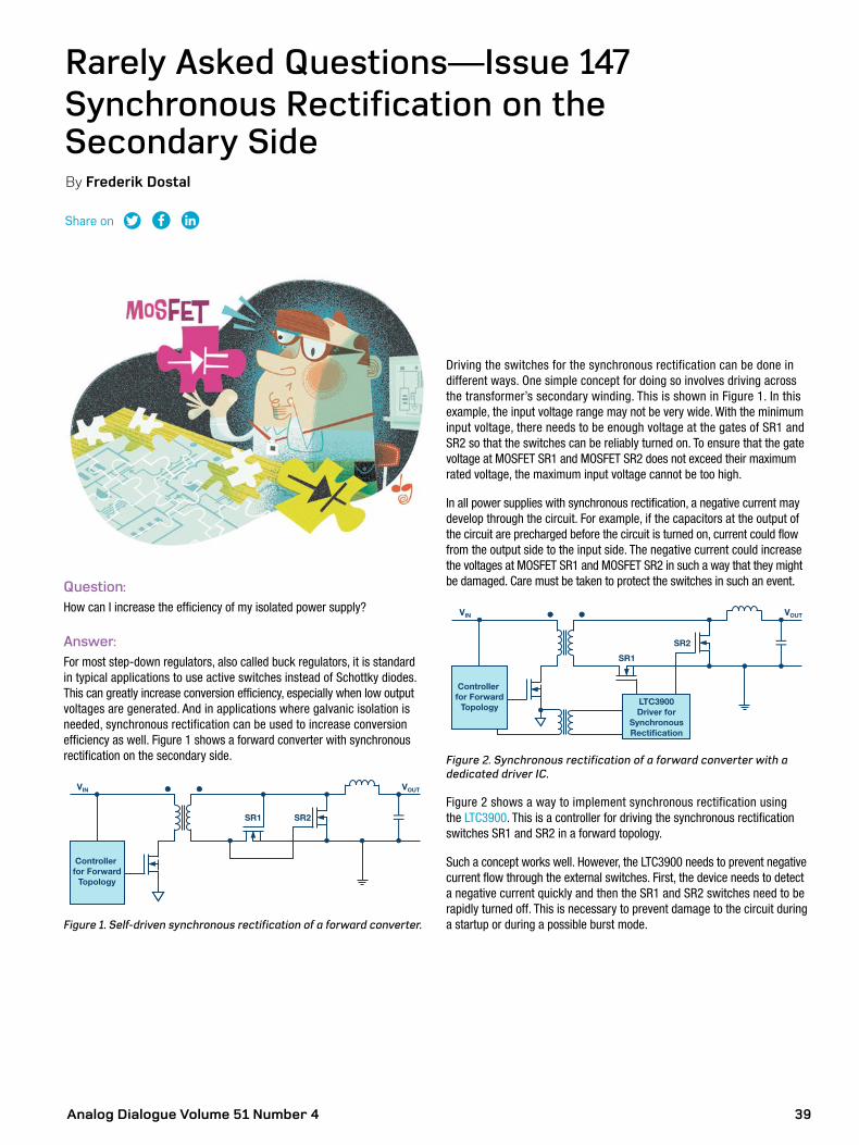
Analog Dialogue Volume 51 Number 4 39
Driving the switches for the synchronous rectification can be done in different ways. One simple concept for doing so involves driving across the transformer’s secondary winding. This is shown in Figure 1. In this example, the input voltage range may not be very wide. With the minimum input voltage, there needs to be enough voltage at the gates of SR1 and SR2 so that the switches can be reliably turned on. To ensure that the gate voltage at MOSFET SR1 and MOSFET SR2 does not exceed their maximum rated voltage, the maximum input voltage cannot be too high.
In all power supplies with synchronous rectification, a negative current may develop through the circuit. For example, if the capacitors at the output of the circuit are precharged before the circuit is turned on, current could flow from the output side to the input side. The negative current could increase the voltages at MOSFET SR1 and MOSFET SR2 in such a way that they might be damaged. Care must be taken to protect the switches in such an event.
VIN
SR1
SR2
VOUT
Controller for Forward
TopologyLTC3900Driver for
SynchronousRectification
Figure 2. Synchronous rectification of a forward converter with a dedicated driver IC.
Figure 2 shows a way to implement synchronous rectification using the LTC3900. This is a controller for driving the synchronous rectification switches SR1 and SR2 in a forward topology.
Such a concept works well. However, the LTC3900 needs to prevent negative current flow through the external switches. First, the device needs to detect a negative current quickly and then the SR1 and SR2 switches need to be rapidly turned off. This is necessary to prevent damage to the circuit during a startup or during a possible burst mode.
Question:How can I increase the efficiency of my isolated power supply?
Answer:For most step-down regulators, also called buck regulators, it is standard in typical applications to use active switches instead of Schottky diodes. This can greatly increase conversion efficiency, especially when low output voltages are generated. And in applications where galvanic isolation is needed, synchronous rectification can be used to increase conversion efficiency as well. Figure 1 shows a forward converter with synchronous rectification on the secondary side.
VIN
SR1 SR2
VOUT
Controller for Forward
Topology
Figure 1. Self-driven synchronous rectification of a forward converter.
Rarely Asked Questions—Issue 147Synchronous Rectification on the Secondary SideBy Frederik Dostal
Share on
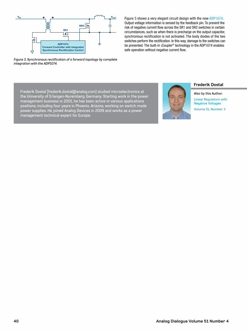
Analog Dialogue Volume 51 Number 440
VIN
SR1
SR2
VOUT
ADP1074Forward Controller with IntegratedSynchronous Rectification Control
Figure 3. Synchronous rectification of a forward topology by complete integration with the ADP1074.
Figure 3 shows a very elegant circuit design with the new ADP1074. Output voltage information is sensed by the feedback pin. To prevent the risk of negative current flow across the SR1 and SR2 switches in certain circumstances, such as when there is precharge on the output capacitor, synchronous rectification is not activated. The body diodes of the two switches perform the rectification. In this way, damage to the switches can be prevented. The built-in iCoupler® technology in the ADP1074 enables safe operation without negative current flow.
Also by this Author:
Linear Regulators with Negative Voltages
Volume 51, Number 3
Frederik Dostal [[email protected]] studied microelectronics at the University of Erlangen-Nuremberg, Germany. Starting work in the power management business in 2001, he has been active in various applications positions, including four years in Phoenix, Arizona, working on switch mode power supplies. He joined Analog Devices in 2009 and works as a power management technical expert for Europe.
Frederik Dostal
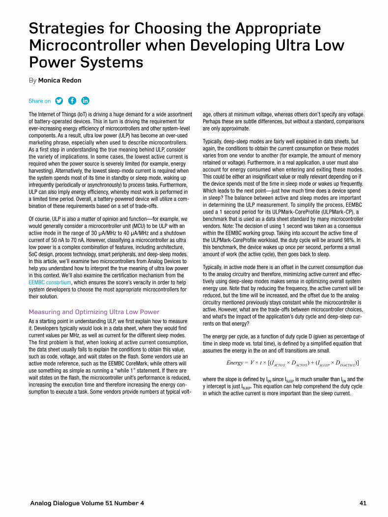
Analog Dialogue Volume 51 Number 4 41
Share on
age, others at minimum voltage, whereas others don’t specify any voltage. Perhaps these are subtle differences, but without a standard, comparisons are only approximate.
Typically, deep-sleep modes are fairly well explained in data sheets, but again, the conditions to obtain the current consumption on these modes varies from one vendor to another (for example, the amount of memory retained or voltage). Furthermore, in a real application, a user must also account for energy consumed when entering and exiting these modes. This could be either an insignificant value or really relevant depending on if the device spends most of the time in sleep mode or wakes up frequently. Which leads to the next point—just how much time does a device spend in sleep? The balance between active and sleep modes are important in determining the ULP measurement. To simplify the process, EEMBC used a 1 second period for its ULPMark-CoreProfile (ULPMark-CP), a benchmark that is used as a data sheet standard by many microcontroller vendors. Note: The decision of using 1 second was taken as a consensus within the EEMBC working group. Taking into account the active time of the ULPMark-CoreProfile workload, the duty cycle will be around 98%. In this benchmark, the device wakes up once per second, performs a small amount of work (the active cycle), then goes back to sleep.
Typically, in active mode there is an offset in the current consumption due to the analog circuitry and therefore, minimizing active current and effec-tively using deep-sleep modes makes sense in optimizing overall system energy use. Note that by reducing the frequency, the active current will be reduced, but the time will be increased, and the offset due to the analog circuitry mentioned previously stays constant while the microcontroller is active. However, what are the trade-offs between microcontroller choices, and what’s the impact of the application’s duty cycle and deep-sleep cur-rents on that energy?
The energy per cycle, as a function of duty cycle D (given as percentage of time in sleep mode vs. total time), is defined by a simplified equation that assumes the energy in the on and off transitions are small.
Energy = V × t × [(IACTIVE × DACTIVE) + (ISLEEP × DINACTIVE)]
where the slope is defined by ION since ISLEEP is much smaller than ION and the y intercept is just ISLEEP. This equation can help comprehend the duty cycle in which the active current is more important than the sleep current.
The Internet of Things (IoT) is driving a huge demand for a wide assortment of battery-operated devices. This in turn is driving the requirement for ever-increasing energy efficiency of microcontrollers and other system-level components. As a result, ultra low power (ULP) has become an over-used marketing phrase, especially when used to describe microcontrollers. As a first step in understanding the true meaning behind ULP, consider the variety of implications. In some cases, the lowest active current is required when the power source is severely limited (for example, energy harvesting). Alternatively, the lowest sleep-mode current is required when the system spends most of its time in standby or sleep mode, waking up infrequently (periodically or asynchronously) to process tasks. Furthermore, ULP can also imply energy efficiency, whereby most work is performed in a limited time period. Overall, a battery-powered device will utilize a com-bination of these requirements based on a set of trade-offs.
Of course, ULP is also a matter of opinion and function—for example, we would generally consider a microcontroller unit (MCU) to be ULP with an active mode in the range of 30 μA/MHz to 40 μA/MHz and a shutdown current of 50 nA to 70 nA. However, classifying a microcontroller as ultra low power is a complex combination of features, including architecture, SoC design, process technology, smart peripherals, and deep-sleep modes. In this article, we’ll examine two microcontrollers from Analog Devices to help you understand how to interpret the true meaning of ultra low power in this context. We’ll also examine the certification mechanism from the EEMBC consortium, which ensures the score’s veracity in order to help system developers to choose the most appropriate microcontrollers for their solution.
Measuring and Optimizing Ultra Low PowerAs a starting point in understanding ULP, we first explain how to measure it. Developers typically would look in a data sheet, where they would find current values per MHz, as well as current for the different sleep modes. The first problem is that, when looking at active current consumption, the data sheet usually fails to explain the conditions to obtain this value, such as code, voltage, and wait states on the flash. Some vendors use an active mode reference, such as the EEMBC CoreMark, while others will use something as simple as running a “while 1” statement. If there are wait states on the flash, the microcontroller unit’s performance is reduced, increasing the execution time and therefore increasing the energy con-sumption to execute a task. Some vendors provide numbers at typical volt-
Strategies for Choosing the Appropriate Microcontroller when Developing Ultra Low Power SystemsBy Monica Redon
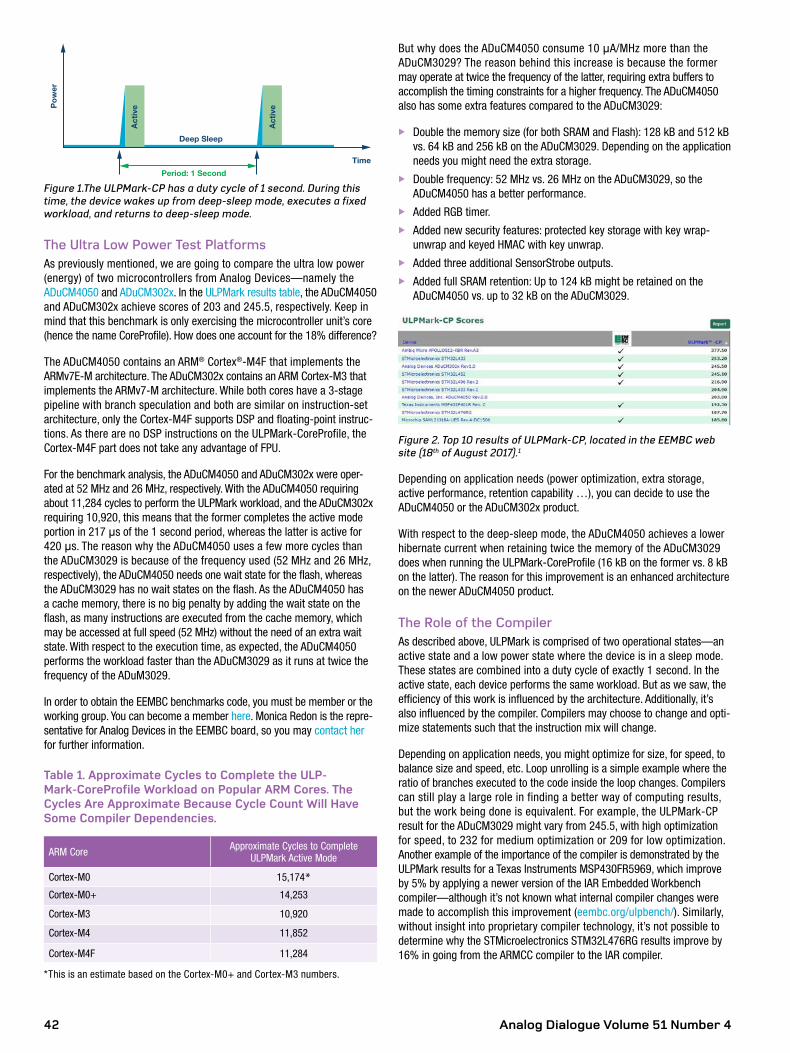
Analog Dialogue Volume 51 Number 442
Po
wer
Deep Sleep
Period: 1 Second
Time
Act
ive
Act
ive
Figure 1.The ULPMark-CP has a duty cycle of 1 second. During this time, the device wakes up from deep-sleep mode, executes a fixed workload, and returns to deep-sleep mode.
The Ultra Low Power Test PlatformsAs previously mentioned, we are going to compare the ultra low power (energy) of two microcontrollers from Analog Devices—namely the ADuCM4050 and ADuCM302x. In the ULPMark results table, the ADuCM4050 and ADuCM302x achieve scores of 203 and 245.5, respectively. Keep in mind that this benchmark is only exercising the microcontroller unit’s core (hence the name CoreProfile). How does one account for the 18% difference?
The ADuCM4050 contains an ARM® Cortex®-M4F that implements the ARMv7E-M architecture. The ADuCM302x contains an ARM Cortex-M3 that implements the ARMv7-M architecture. While both cores have a 3-stage pipeline with branch speculation and both are similar on instruction-set architecture, only the Cortex-M4F supports DSP and floating-point instruc-tions. As there are no DSP instructions on the ULPMark-CoreProfile, the Cortex-M4F part does not take any advantage of FPU.
For the benchmark analysis, the ADuCM4050 and ADuCM302x were oper-ated at 52 MHz and 26 MHz, respectively. With the ADuCM4050 requiring about 11,284 cycles to perform the ULPMark workload, and the ADuCM302x requiring 10,920, this means that the former completes the active mode portion in 217 μs of the 1 second period, whereas the latter is active for 420 μs. The reason why the ADuCM4050 uses a few more cycles than the ADuCM3029 is because of the frequency used (52 MHz and 26 MHz, respectively), the ADuCM4050 needs one wait state for the flash, whereas the ADuCM3029 has no wait states on the flash. As the ADuCM4050 has a cache memory, there is no big penalty by adding the wait state on the flash, as many instructions are executed from the cache memory, which may be accessed at full speed (52 MHz) without the need of an extra wait state. With respect to the execution time, as expected, the ADuCM4050 performs the workload faster than the ADuCM3029 as it runs at twice the frequency of the ADuM3029.
In order to obtain the EEMBC benchmarks code, you must be member or the working group. You can become a member here. Monica Redon is the repre-sentative for Analog Devices in the EEMBC board, so you may contact her for further information.
Table 1. Approximate Cycles to Complete the ULP-Mark-CoreProfile Workload on Popular ARM Cores. The Cycles Are Approximate Because Cycle Count Will Have Some Compiler Dependencies.
ARM Core Approximate Cycles to Complete ULPMark Active Mode
Cortex-M0 15,174*
Cortex-M0+ 14,253
Cortex-M3 10,920
Cortex-M4 11,852
Cortex-M4F 11,284
*This is an estimate based on the Cortex-M0+ and Cortex-M3 numbers.
But why does the ADuCM4050 consume 10 μA/MHz more than the ADuCM3029? The reason behind this increase is because the former may operate at twice the frequency of the latter, requiring extra buffers to accomplish the timing constraints for a higher frequency. The ADuCM4050 also has some extra features compared to the ADuCM3029:
X Double the memory size (for both SRAM and Flash): 128 kB and 512 kB vs. 64 kB and 256 kB on the ADuCM3029. Depending on the application needs you might need the extra storage.
X Double frequency: 52 MHz vs. 26 MHz on the ADuCM3029, so the ADuCM4050 has a better performance.
X Added RGB timer. X Added new security features: protected key storage with key wrap-
unwrap and keyed HMAC with key unwrap. X Added three additional SensorStrobe outputs. X Added full SRAM retention: Up to 124 kB might be retained on the
ADuCM4050 vs. up to 32 kB on the ADuCM3029.
Figure 2. Top 10 results of ULPMark-CP, located in the EEMBC web site (18th of August 2017).1
Depending on application needs (power optimization, extra storage, active performance, retention capability …), you can decide to use the ADuCM4050 or the ADuCM302x product.
With respect to the deep-sleep mode, the ADuCM4050 achieves a lower hibernate current when retaining twice the memory of the ADuCM3029 does when running the ULPMark-CoreProfile (16 kB on the former vs. 8 kB on the latter). The reason for this improvement is an enhanced architecture on the newer ADuCM4050 product.
The Role of the CompilerAs described above, ULPMark is comprised of two operational states—an active state and a low power state where the device is in a sleep mode. These states are combined into a duty cycle of exactly 1 second. In the active state, each device performs the same workload. But as we saw, the efficiency of this work is influenced by the architecture. Additionally, it’s also influenced by the compiler. Compilers may choose to change and opti-mize statements such that the instruction mix will change.
Depending on application needs, you might optimize for size, for speed, to balance size and speed, etc. Loop unrolling is a simple example where the ratio of branches executed to the code inside the loop changes. Compilers can still play a large role in finding a better way of computing results, but the work being done is equivalent. For example, the ULPMark-CP result for the ADuCM3029 might vary from 245.5, with high optimization for speed, to 232 for medium optimization or 209 for low optimization. Another example of the importance of the compiler is demonstrated by the ULPMark results for a Texas Instruments MSP430FR5969, which improve by 5% by applying a newer version of the IAR Embedded Workbench compiler—although it’s not known what internal compiler changes were made to accomplish this improvement (eembc.org/ulpbench/). Similarly, without insight into proprietary compiler technology, it’s not possible to determine why the STMicroelectronics STM32L476RG results improve by 16% in going from the ARMCC compiler to the IAR compiler.
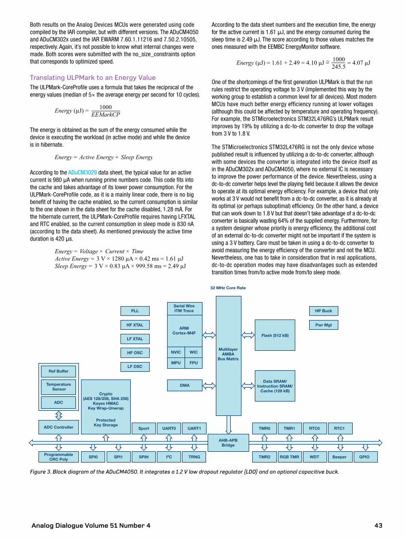
Analog Dialogue Volume 51 Number 4 43
Both results on the Analog Devices MCUs were generated using code compiled by the IAR compiler, but with different versions. The ADuCM4050 and ADuCM302x used the IAR EWARM 7.60.1.11216 and 7.50.2.10505, respectively. Again, it’s not possible to know what internal changes were made. Both scores were submitted with the no_size_constraints option that corresponds to optimized speed.
Translating ULPMark to an Energy ValueThe ULPMark-CoreProfile uses a formula that takes the reciprocal of the energy values (median of 5× the average energy per second for 10 cycles).
Energy (µJ) = 1000
EEMarkCP
The energy is obtained as the sum of the energy consumed while the device is executing the workload (in active mode) and while the device is in hibernate.
Energy = Active Energy + Sleep Energy
According to the ADuCM3029 data sheet, the typical value for an active current is 980 μA when running prime numbers code. This code fits into the cache and takes advantage of its lower power consumption. For the ULPMark-CoreProfile code, as it is a mainly linear code, there is no big benefit of having the cache enabled, so the current consumption is similar to the one shown in the data sheet for the cache disabled, 1.28 mA. For the hibernate current, the ULPMark-CoreProfile requires having LFXTAL and RTC enabled, so the current consumption in sleep mode is 830 nA (according to the data sheet). As mentioned previously the active time duration is 420 μs.
Energy = Voltage × Current × TimeActive Energy = 3 V × 1280 μA × 0.42 ms = 1.61 μJSleep Energy = 3 V × 0.83 μA × 999.58 ms = 2.49 μJ
According to the data sheet numbers and the execution time, the energy for the active current is 1.61 μJ, and the energy consumed during the sleep time is 2.49 μJ. The score according to those values matches the ones measured with the EEMBC EnergyMonitor software.
Energy (μJ) = 1.61 + 2.49 = 4.10 μJ =~ = 4.07 μJ1000
245.5
One of the shortcomings of the first generation ULPMark is that the run rules restrict the operating voltage to 3 V (implemented this way by the working group to establish a common level for all devices). Most modern MCUs have much better energy efficiency running at lower voltages (although this could be affected by temperature and operating frequency). For example, the STMicroelectronics STM32L476RG’s ULPMark result improves by 19% by utilizing a dc-to-dc converter to drop the voltage from 3 V to 1.8 V.
The STMicroelectronics STM32L476RG is not the only device whose published result is influenced by utilizing a dc-to-dc converter, although with some devices the converter is integrated into the device itself as in the ADuCM302x and ADuCM4050, where no external IC is necessary to improve the power performance of the device. Nevertheless, using a dc-to-dc converter helps level the playing field because it allows the device to operate at its optimal energy efficiency. For example, a device that only works at 3 V would not benefit from a dc-to-dc converter, as it is already at its optimal (or perhaps suboptimal) efficiency. On the other hand, a device that can work down to 1.8 V but that doesn’t take advantage of a dc-to-dc converter is basically wasting 64% of the supplied energy. Furthermore, for a system designer whose priority is energy efficiency, the additional cost of an external dc-to-dc converter might not be important if the system is using a 3 V battery. Care must be taken in using a dc-to-dc converter to avoid measuring the energy efficiency of the converter and not the MCU. Nevertheless, one has to take in consideration that in real applications, dc-to-dc operation modes may have disadvantages such as extended transition times from/to active mode from/to sleep mode.
Figure 3. Block diagram of the ADuCM4050. It integrates a 1.2 V low dropout regulator (LDO) and an optional capacitive buck.
PLL
HF XTAL
LF XTAL
HF OSC
LF OSCRef Buffer
Crypto(AES 128/256, SHA 256)
Keyes HMACKey Wrap-Unwrap
ProtectedKey Storage
Temperature Sensor
ADC
ADC Controller
ProgrammableCRC Poly SPI0 SPI1 SPIH I2C TRNG
Sport UART0 UART1 TMR0 TMR1 RTC0 RTC1
TMR2 RGB TMR WDT Beeper GPIO
NVIC WIC
ARMCortex-M4F
Serial WireITM Trace
MultilayerAMBA
Bus Matrix
52 MHz Core Rate
AHB-APBBridge
Flash (512 kB)
Data SRAM/Instruction SRAM/
Cache (128 kB)
HP Buck
Pwr Mgt
MPU FPU
DMA
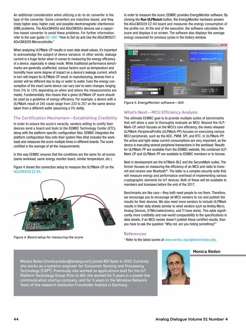
Analog Dialogue Volume 51 Number 444
An additional consideration when utilizing a dc-to-dc converter is the type of the converter. Some converters are inductive-based, and they imply higher area, higher cost, and possible electromagnetic interference (EMI) problems. The ADuCM4050 and ADuCM302x devices use a capaci-tive-based converter to avoid these problems. For further information, refer to the user guide UG-1091 “How to Set Up and Use the ADuCM3027/ADuCM3029 Microcontroller.”
When analyzing ULPMark-CP results or even data sheet values, it’s important to acknowledge the subject of device variance. In other words, leakage current is a huge factor when it comes to measuring the energy efficiency of a device, especially in sleep mode. While traditional performance bench-marks are generally unaffected, various factors such as temperature and humidity have some degree of impact on a device’s leakage current, which in turn will impact its ULPMark-CP result. In manufacturing, devices from a vendor will be different day to day or wafer to wafer. Even the energy con-sumption of the exact same device can vary (we’ve seen changes ranging from 5% to 15% depending on when and where the measurements are made). Fundamentally, this means that a given ULPMark-CP score should be used as a guideline of energy efficiency. For example, a device with a ULPMark result of 245 could range from 233 to 257 on the same device taken from a different wafer (assuming a 5% delta).
The Certification Mechanism—Establishing CredibilityIn order to ensure the score’s veracity, vendors willing to certify their devices send a board and tools to the EEMBC Technology Center (ETC), along with the platform specific configuration files. EEMBC integrates the platform configuration files onto their system files (that includes the work-load) and measures the score multiple times in different boards. The score certified is the average of all the measurements.
In this way EEMBC ensures that the conditions are the same for all scores (same workload, same energy monitor board, similar temperature, etc.).
Figure 4 shows the connection setup to measure the ULPMark-CP on the ADuCM3029 EZ-Kit.
Figure 4. Board setup for measuring the score.
In order to measure the score, EEMBC provides EnergyMonitor software. By clicking the Run ULPBench button, the EnergyMonitor hardware powers the ADuCM3029 EZ-Kit board and measures the energy consumption of the profile run. At the end of the execution, the software calculates the score and displays it on screen. The software also displays the average energy consumed for previous cycles in the history window.
Figure 5. EnergyMonitor software—GUI.
What’s Next—MCU Efficiency AnalysisThe ultimate EEMBC goal is to provide multiple suites of benchmarks that will allow a user to thoroughly evaluate an MCU. Beyond the ULP-Mark-CP, which focuses on the MCU’s core efficiency, the newly released ULPMark-PeripheralProfile (ULPMark-PP) focuses on exercising various MCU peripherals, such as the ADC, PWM, SPI, and RTC. In ULPMark-PP, the active and light-sleep current consumptions are very important, as the device is executing several peripheral transactions in the workload. Results for ULPMark-PP are available from the EEMBC website; the combined ULP-Mark-CP and ULPMark-PP are available to EEMBC members or to license.
Next in development are the IoTMark-BLE and the SecureMark suites. The former focuses on measuring the efficiency of an MCU and radio to trans-mit and receive over Bluetooth®. The latter is a complex security suite that will measure energy and performance overhead of implementing various cryptographic elements for IoT devices. Both of these will be available to members and licensees before the end of the 2017.
Benchmarks are like cars—they both need people to run them. Therefore, we encourage you to encourage all MCU vendors to run and publish the results for their devices. We also need more vendors to include ULPMark results in their data sheets (similar to what vendors such as Ambiq Micro, Analog Devices, STMicroelectronics, and TI have done). This adds signifi-cantly more credibility and real-world comparability to the specifications in data sheets. If an MCU vendor doesn’t publish these certified results, then you have to ask the question “Why not, are you hiding something?”
References1 Refer to the latest scores at www.eembc.org/ulpbench/index.php.
Monica Redon [[email protected]] joined ADI Spain in 2010. Currently she works as a systems engineer for Consumer Sensing and Processing Technology (CSPT). Previously she worked as applications lead for the IoT Platform Technology Group. Prior to ADI, she worked for 5 years in a power-line communication startup company, and for 5 years in the Wireless Network Team of the research institution Fraunhofer-Institut in Germany.
Monica Redon
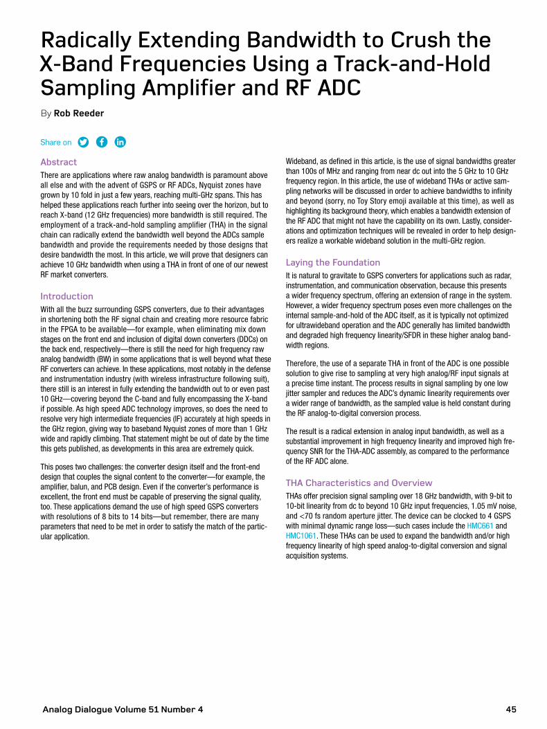
Analog Dialogue Volume 51 Number 4 45
Share on
Wideband, as defined in this article, is the use of signal bandwidths greater than 100s of MHz and ranging from near dc out into the 5 GHz to 10 GHz frequency region. In this article, the use of wideband THAs or active sam-pling networks will be discussed in order to achieve bandwidths to infinity and beyond (sorry, no Toy Story emoji available at this time), as well as highlighting its background theory, which enables a bandwidth extension of the RF ADC that might not have the capability on its own. Lastly, consider-ations and optimization techniques will be revealed in order to help design-ers realize a workable wideband solution in the multi-GHz region.
Laying the FoundationIt is natural to gravitate to GSPS converters for applications such as radar, instrumentation, and communication observation, because this presents a wider frequency spectrum, offering an extension of range in the system. However, a wider frequency spectrum poses even more challenges on the internal sample-and-hold of the ADC itself, as it is typically not optimized for ultrawideband operation and the ADC generally has limited bandwidth and degraded high frequency linearity/SFDR in these higher analog band-width regions.
Therefore, the use of a separate THA in front of the ADC is one possible solution to give rise to sampling at very high analog/RF input signals at a precise time instant. The process results in signal sampling by one low jitter sampler and reduces the ADC’s dynamic linearity requirements over a wider range of bandwidth, as the sampled value is held constant during the RF analog-to-digital conversion process.
The result is a radical extension in analog input bandwidth, as well as a substantial improvement in high frequency linearity and improved high fre-quency SNR for the THA-ADC assembly, as compared to the performance of the RF ADC alone.
THA Characteristics and OverviewTHAs offer precision signal sampling over 18 GHz bandwidth, with 9-bit to 10-bit linearity from dc to beyond 10 GHz input frequencies, 1.05 mV noise, and <70 fs random aperture jitter. The device can be clocked to 4 GSPS with minimal dynamic range loss—such cases include the HMC661 and HMC1061. These THAs can be used to expand the bandwidth and/or high frequency linearity of high speed analog-to-digital conversion and signal acquisition systems.
AbstractThere are applications where raw analog bandwidth is paramount above all else and with the advent of GSPS or RF ADCs, Nyquist zones have grown by 10 fold in just a few years, reaching multi-GHz spans. This has helped these applications reach further into seeing over the horizon, but to reach X-band (12 GHz frequencies) more bandwidth is still required. The employment of a track-and-hold sampling amplifier (THA) in the signal chain can radically extend the bandwidth well beyond the ADCs sample bandwidth and provide the requirements needed by those designs that desire bandwidth the most. In this article, we will prove that designers can achieve 10 GHz bandwidth when using a THA in front of one of our newest RF market converters.
IntroductionWith all the buzz surrounding GSPS converters, due to their advantages in shortening both the RF signal chain and creating more resource fabric in the FPGA to be available—for example, when eliminating mix down stages on the front end and inclusion of digital down converters (DDCs) on the back end, respectively—there is still the need for high frequency raw analog bandwidth (BW) in some applications that is well beyond what these RF converters can achieve. In these applications, most notably in the defense and instrumentation industry (with wireless infrastructure following suit), there still is an interest in fully extending the bandwidth out to or even past 10 GHz—covering beyond the C-band and fully encompassing the X-band if possible. As high speed ADC technology improves, so does the need to resolve very high intermediate frequencies (IF) accurately at high speeds in the GHz region, giving way to baseband Nyquist zones of more than 1 GHz wide and rapidly climbing. That statement might be out of date by the time this gets published, as developments in this area are extremely quick.
This poses two challenges: the converter design itself and the front-end design that couples the signal content to the converter—for example, the amplifier, balun, and PCB design. Even if the converter’s performance is excellent, the front end must be capable of preserving the signal quality, too. These applications demand the use of high speed GSPS converters with resolutions of 8 bits to 14 bits—but remember, there are many parameters that need to be met in order to satisfy the match of the partic-ular application.
Radically Extending Bandwidth to Crush the X-Band Frequencies Using a Track-and-Hold Sampling Amplifier and RF ADCBy Rob Reeder
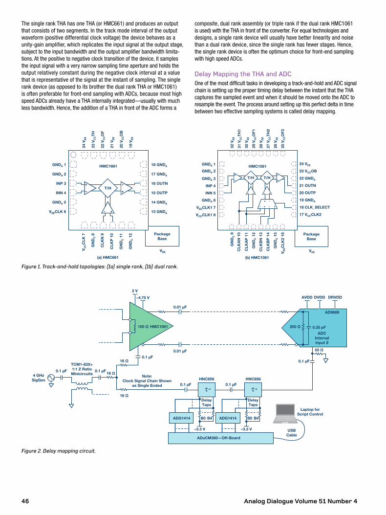
Analog Dialogue Volume 51 Number 446
The single rank THA has one THA (or HMC661) and produces an output that consists of two segments. In the track mode interval of the output waveform (positive differential clock voltage) the device behaves as a unity-gain amplifier, which replicates the input signal at the output stage, subject to the input bandwidth and the output amplifier bandwidth limita-tions. At the positive to negative clock transition of the device, it samples the input signal with a very narrow sampling time aperture and holds the output relatively constant during the negative clock interval at a value that is representative of the signal at the instant of sampling. The single rank device (as opposed to its brother the dual rank THA or HMC1061) is often preferable for front-end sampling with ADCs, because most high speed ADCs already have a THA internally integrated—usually with much less bandwidth. Hence, the addition of a THA in front of the ADC forms a
composite, dual rank assembly (or triple rank if the dual rank HMC1061 is used) with the THA in front of the converter. For equal technologies and designs, a single rank device will usually have better linearity and noise than a dual rank device, since the single rank has fewer stages. Hence, the single rank device is often the optimum choice for front-end sampling with high speed ADCs.
Delay Mapping the THA and ADCOne of the most difficult tasks in developing a track-and-hold and ADC signal chain is setting up the proper timing delay between the instant that the THA captures the sampled event and when it should be moved onto the ADC to resample the event. The process around setting up this perfect delta in time between two effective sampling systems is called delay mapping.
24 V
EE
VEE
23 V
CCT
H
22 V
CCO
F
21 V
EE
20 V
CCO
B
19 V
EE
18 GNDA
17 GNDA
16 OUTN
15 OUTP
14 GNDA
13 GNDA
GNDA 1 HMC1661
PackageBase
GNDA 2
INP 3
INN 4
GNDA 5
VEECLK 6
VC
CC
LK 7
GN
DC 8
CLK
N 9
CLK
P 1
0
GN
DC 1
1
GN
DC 1
2
T/H
(a) HMC661
32 V
EE
31 V
CCT
H1
30 V
EE
29 V
CCO
F1
28 V
EE
27 V
CCT
H2
26 V
EE
25 V
CCO
F2
24 VEE
23 VCCOB
22 GNDA
21 OUTN
20 OUTP
19 GNDA
18 CLK_SELECT
17 VCCCLK2
VEE
GNDA 1
GNDA 2
GNDA 3
INP 4
INN 5
GNDA 6
VEECLK1 7
VCCCLK1 8
HMC1061
PackageBase
(b) HMC1061
GN
DC 9
CLK
AN
10
CLK
AP
11
GN
DC 1
2
CLK
BN
13
CLK
BP
14
GN
DC 1
5
VE
EC
LK2
16
T/H T/H
Figure 1. Track-and-hold topologies: (1a) single rank, (1b) dual rank.
2 V
–4.75 V
0.01 µF
AVDD DVDD DRVDD
AD9689
ADCInternalInput Z
100 Ω HMC1061
16 Ω
HNC856Note:
Clock Signal Chain Shownas Single Ended
16 Ω
16 Ω
200 Ω 0.35 pF
0.01 µF
0.1 µF
0.1 µF 0.1 µF
–3.3 V
B0 B4
DelayTaps
0.1 µF
50 Ω
0.1 µF4 GHz
SigGen
TCM1-83X+1:1 Z RatioMinicircuits
0.1 µF
τ–x
HNC856
τ–x
–3.3 V
B0 B4
DelayTaps
ADG1414
ADuCM360—Off-Board
USBCable
Laptop forScript Control
ADG1414
Figure 2. Delay mapping circuit.
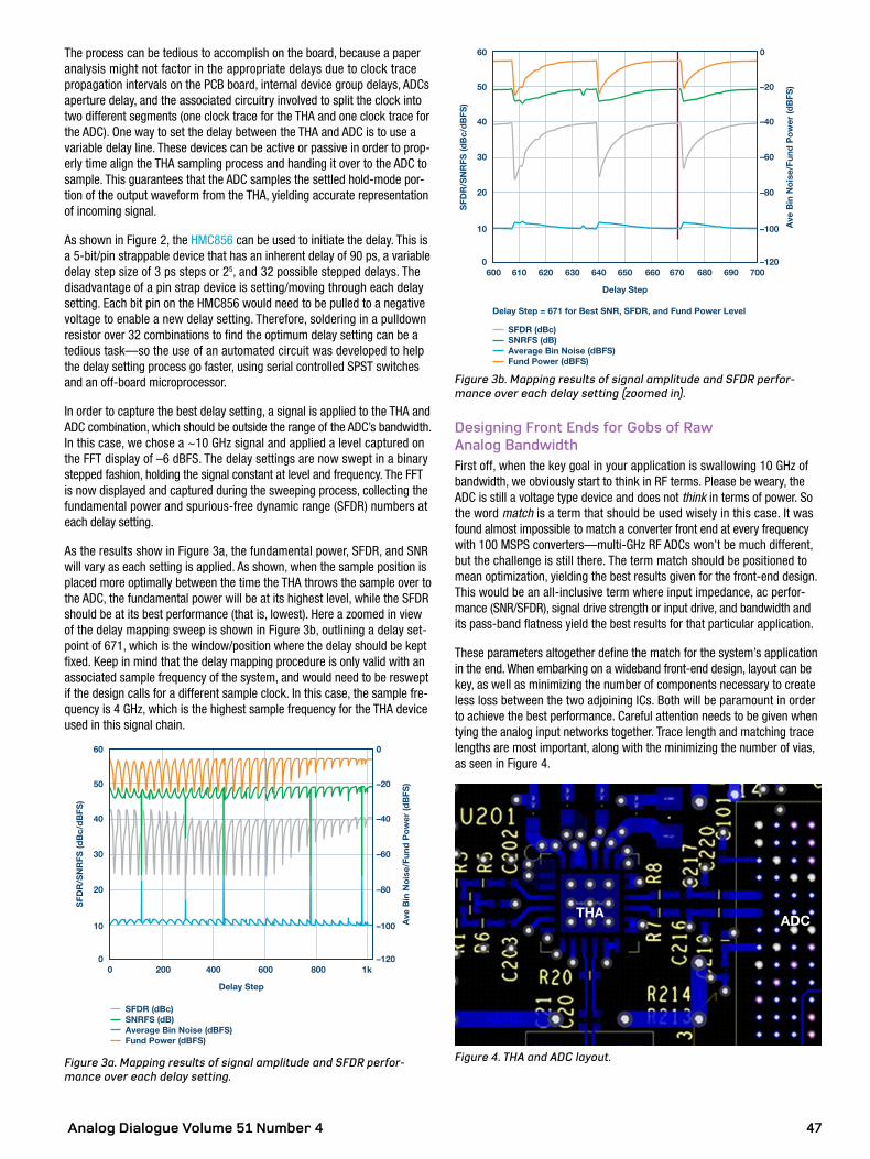
Analog Dialogue Volume 51 Number 4 47
The process can be tedious to accomplish on the board, because a paper analysis might not factor in the appropriate delays due to clock trace propagation intervals on the PCB board, internal device group delays, ADCs aperture delay, and the associated circuitry involved to split the clock into two different segments (one clock trace for the THA and one clock trace for the ADC). One way to set the delay between the THA and ADC is to use a variable delay line. These devices can be active or passive in order to prop-erly time align the THA sampling process and handing it over to the ADC to sample. This guarantees that the ADC samples the settled hold-mode por-tion of the output waveform from the THA, yielding accurate representation of incoming signal.
As shown in Figure 2, the HMC856 can be used to initiate the delay. This is a 5-bit/pin strappable device that has an inherent delay of 90 ps, a variable delay step size of 3 ps steps or 25, and 32 possible stepped delays. The disadvantage of a pin strap device is setting/moving through each delay setting. Each bit pin on the HMC856 would need to be pulled to a negative voltage to enable a new delay setting. Therefore, soldering in a pulldown resistor over 32 combinations to find the optimum delay setting can be a tedious task—so the use of an automated circuit was developed to help the delay setting process go faster, using serial controlled SPST switches and an off-board microprocessor.
In order to capture the best delay setting, a signal is applied to the THA and ADC combination, which should be outside the range of the ADC’s bandwidth. In this case, we chose a ~10 GHz signal and applied a level captured on the FFT display of –6 dBFS. The delay settings are now swept in a binary stepped fashion, holding the signal constant at level and frequency. The FFT is now displayed and captured during the sweeping process, collecting the fundamental power and spurious-free dynamic range (SFDR) numbers at each delay setting.
As the results show in Figure 3a, the fundamental power, SFDR, and SNR will vary as each setting is applied. As shown, when the sample position is placed more optimally between the time the THA throws the sample over to the ADC, the fundamental power will be at its highest level, while the SFDR should be at its best performance (that is, lowest). Here a zoomed in view of the delay mapping sweep is shown in Figure 3b, outlining a delay set-point of 671, which is the window/position where the delay should be kept fixed. Keep in mind that the delay mapping procedure is only valid with an associated sample frequency of the system, and would need to be reswept if the design calls for a different sample clock. In this case, the sample fre-quency is 4 GHz, which is the highest sample frequency for the THA device used in this signal chain.
50
40
20
30
10
0
60
0 200 400 600 800 1k
SFD
R/S
NR
FS (d
Bc/
dB
FS)
–20
–40
–80
–60
–100
–120
0
Ave
Bin
No
ise/
Fund
Po
wer
(dB
FS)
Delay Step
SFDR (dBc)SNRFS (dB)Average Bin Noise (dBFS)Fund Power (dBFS)
Figure 3a. Mapping results of signal amplitude and SFDR perfor-mance over each delay setting.
50
40
20
30
10
0
60
600 610 620 630 640 650 660 670 680 690 700
SFD
R/S
NR
FS (d
Bc/
dB
FS)
–20
–40
–80
–60
–100
–120
0
Ave
Bin
No
ise/
Fund
Po
wer
(dB
FS)
Delay Step
Delay Step = 671 for Best SNR, SFDR, and Fund Power Level
SFDR (dBc)SNRFS (dB)Average Bin Noise (dBFS)Fund Power (dBFS)
Figure 3b. Mapping results of signal amplitude and SFDR perfor-mance over each delay setting (zoomed in).
Designing Front Ends for Gobs of Raw Analog BandwidthFirst off, when the key goal in your application is swallowing 10 GHz of bandwidth, we obviously start to think in RF terms. Please be weary, the ADC is still a voltage type device and does not think in terms of power. So the word match is a term that should be used wisely in this case. It was found almost impossible to match a converter front end at every frequency with 100 MSPS converters—multi-GHz RF ADCs won’t be much different, but the challenge is still there. The term match should be positioned to mean optimization, yielding the best results given for the front-end design. This would be an all-inclusive term where input impedance, ac perfor-mance (SNR/SFDR), signal drive strength or input drive, and bandwidth and its pass-band flatness yield the best results for that particular application.
These parameters altogether define the match for the system’s application in the end. When embarking on a wideband front-end design, layout can be key, as well as minimizing the number of components necessary to create less loss between the two adjoining ICs. Both will be paramount in order to achieve the best performance. Careful attention needs to be given when tying the analog input networks together. Trace length and matching trace lengths are most important, along with the minimizing the number of vias, as seen in Figure 4.
THA ADC
Figure 4. THA and ADC layout.
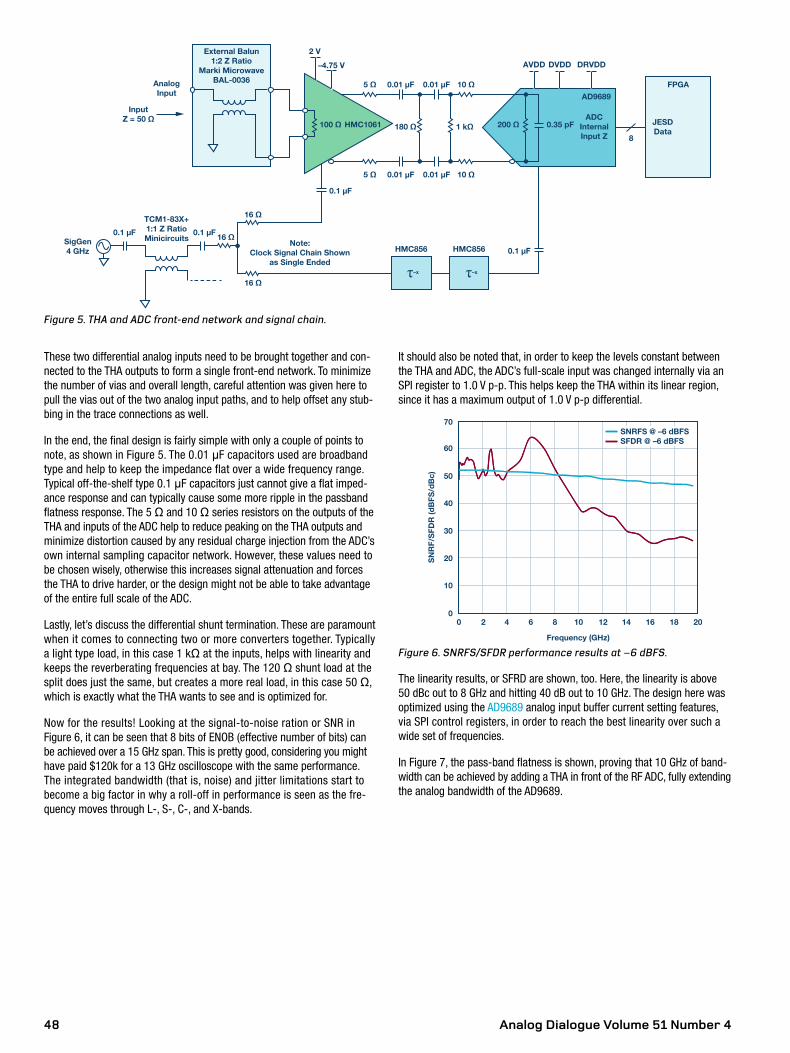
Analog Dialogue Volume 51 Number 448
These two differential analog inputs need to be brought together and con-nected to the THA outputs to form a single front-end network. To minimize the number of vias and overall length, careful attention was given here to pull the vias out of the two analog input paths, and to help offset any stub-bing in the trace connections as well.
In the end, the final design is fairly simple with only a couple of points to note, as shown in Figure 5. The 0.01 µF capacitors used are broadband type and help to keep the impedance flat over a wide frequency range. Typical off-the-shelf type 0.1 µF capacitors just cannot give a flat imped-ance response and can typically cause some more ripple in the passband flatness response. The 5 Ω and 10 Ω series resistors on the outputs of the THA and inputs of the ADC help to reduce peaking on the THA outputs and minimize distortion caused by any residual charge injection from the ADC’s own internal sampling capacitor network. However, these values need to be chosen wisely, otherwise this increases signal attenuation and forces the THA to drive harder, or the design might not be able to take advantage of the entire full scale of the ADC.
Lastly, let’s discuss the differential shunt termination. These are paramount when it comes to connecting two or more converters together. Typically a light type load, in this case 1 kΩ at the inputs, helps with linearity and keeps the reverberating frequencies at bay. The 120 Ω shunt load at the split does just the same, but creates a more real load, in this case 50 Ω, which is exactly what the THA wants to see and is optimized for.
Now for the results! Looking at the signal-to-noise ration or SNR in Figure 6, it can be seen that 8 bits of ENOB (effective number of bits) can be achieved over a 15 GHz span. This is pretty good, considering you might have paid $120k for a 13 GHz oscilloscope with the same performance. The integrated bandwidth (that is, noise) and jitter limitations start to become a big factor in why a roll-off in performance is seen as the fre-quency moves through L-, S-, C-, and X-bands.
It should also be noted that, in order to keep the levels constant between the THA and ADC, the ADC’s full-scale input was changed internally via an SPI register to 1.0 V p-p. This helps keep the THA within its linear region, since it has a maximum output of 1.0 V p-p differential.
20
10
0
30
40
50
60
70
0 2 4 6 8 10 12 14 16 18 20
SN
RF/
SFD
R (d
BFS
/dB
c)
Frequency (GHz)
SNRFS @ –6 dBFSSFDR @ –6 dBFS
Figure 6. SNRFS/SFDR performance results at –6 dBFS.
The linearity results, or SFRD are shown, too. Here, the linearity is above 50 dBc out to 8 GHz and hitting 40 dB out to 10 GHz. The design here was optimized using the AD9689 analog input buffer current setting features, via SPI control registers, in order to reach the best linearity over such a wide set of frequencies.
In Figure 7, the pass-band flatness is shown, proving that 10 GHz of band-width can be achieved by adding a THA in front of the RF ADC, fully extending the analog bandwidth of the AD9689.
5 Ω
2 V
–4.75 V
0.01 µF
AVDD DVDD DRVDD
AD9689
ADCInternalInput Z
JESDData
FPGA
200 Ω100 Ω HMC1061 0.35 pF
0.01 µF 10 Ω
1 kΩ180 Ω
5 Ω
16 Ω
HMC856 HMC856Note:
Clock Signal Chain Shownas Single Ended
16 Ω
16 Ω
8
0.01 µF 0.01 µF
0.1 µF
0.1 µFSigGen4 GHz
TCM1-83X+1:1 Z RatioMinicircuits
AnalogInput
External Balun1:2 Z Ratio
Marki MicrowaveBAL-0036
InputZ = 50 Ω
0.1 µF
0.1 µF
10 Ω
τ–xτ–x
Figure 5. THA and ADC front-end network and signal chain.
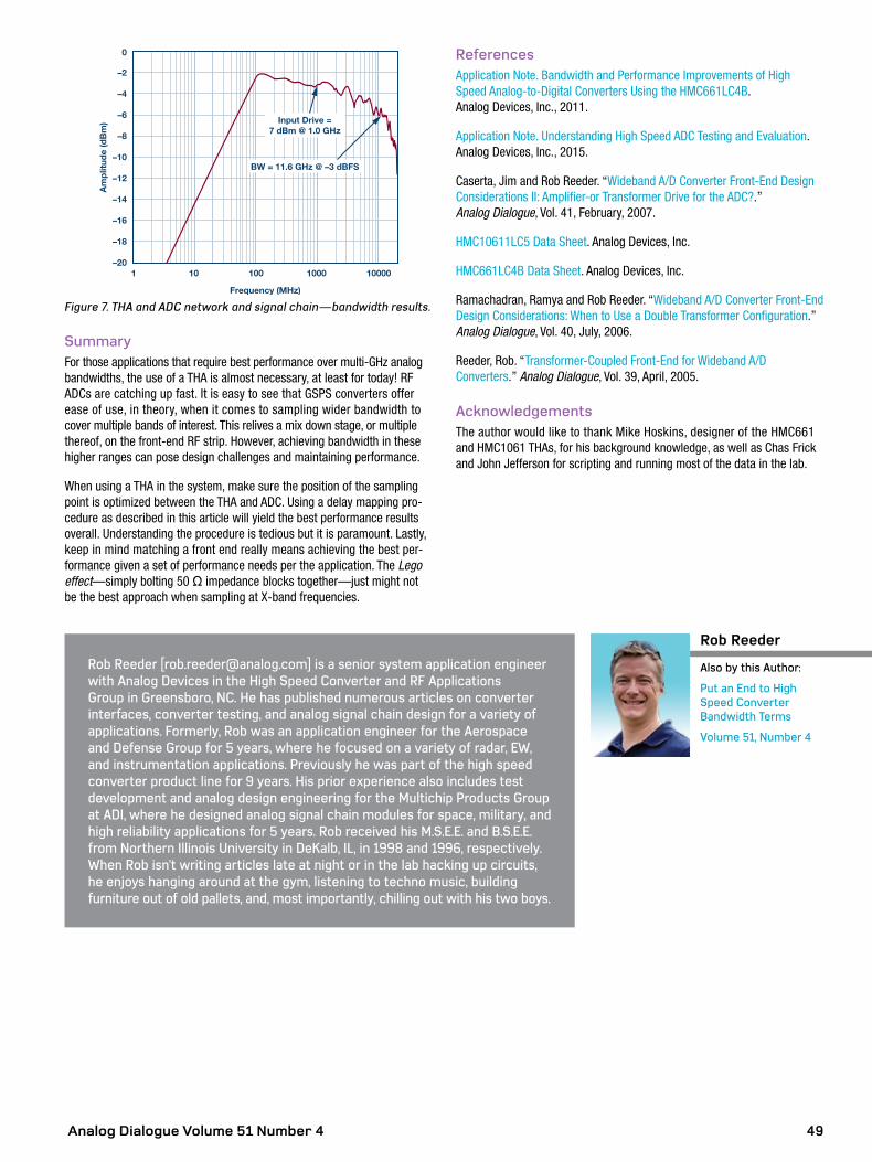
Analog Dialogue Volume 51 Number 4 49
Rob Reeder [[email protected]] is a senior system application engineer with Analog Devices in the High Speed Converter and RF Applications Group in Greensboro, NC. He has published numerous articles on converter interfaces, converter testing, and analog signal chain design for a variety of applications. Formerly, Rob was an application engineer for the Aerospace and Defense Group for 5 years, where he focused on a variety of radar, EW, and instrumentation applications. Previously he was part of the high speed converter product line for 9 years. His prior experience also includes test development and analog design engineering for the Multichip Products Group at ADI, where he designed analog signal chain modules for space, military, and high reliability applications for 5 years. Rob received his M.S.E.E. and B.S.E.E. from Northern Illinois University in DeKalb, IL, in 1998 and 1996, respectively. When Rob isn’t writing articles late at night or in the lab hacking up circuits, he enjoys hanging around at the gym, listening to techno music, building furniture out of old pallets, and, most importantly, chilling out with his two boys.
Rob Reeder
Also by this Author:
Put an End to High Speed Converter Bandwidth Terms
Volume 51, Number 4
–2
–4
–6
–8
–10
–12
–14
–16
–18
–20
0
1 10 100 1000 10000
Am
plit
ude
(dB
m)
Frequency (MHz)
Input Drive =7 dBm @ 1.0 GHz
BW = 11.6 GHz @ –3 dBFS
Figure 7. THA and ADC network and signal chain—bandwidth results.
SummaryFor those applications that require best performance over multi-GHz analog bandwidths, the use of a THA is almost necessary, at least for today! RF ADCs are catching up fast. It is easy to see that GSPS converters offer ease of use, in theory, when it comes to sampling wider bandwidth to cover multiple bands of interest. This relives a mix down stage, or multiple thereof, on the front-end RF strip. However, achieving bandwidth in these higher ranges can pose design challenges and maintaining performance.
When using a THA in the system, make sure the position of the sampling point is optimized between the THA and ADC. Using a delay mapping pro-cedure as described in this article will yield the best performance results overall. Understanding the procedure is tedious but it is paramount. Lastly, keep in mind matching a front end really means achieving the best per-formance given a set of performance needs per the application. The Lego effect—simply bolting 50 Ω impedance blocks together—just might not be the best approach when sampling at X-band frequencies.
ReferencesApplication Note. Bandwidth and Performance Improvements of High Speed Analog-to-Digital Converters Using the HMC661LC4B. Analog Devices, Inc., 2011.
Application Note. Understanding High Speed ADC Testing and Evaluation. Analog Devices, Inc., 2015.
Caserta, Jim and Rob Reeder. “Wideband A/D Converter Front-End Design Considerations II: Amplifier-or Transformer Drive for the ADC?.” Analog Dialogue, Vol. 41, February, 2007.
HMC10611LC5 Data Sheet. Analog Devices, Inc.
HMC661LC4B Data Sheet. Analog Devices, Inc.
Ramachadran, Ramya and Rob Reeder. “Wideband A/D Converter Front-End Design Considerations: When to Use a Double Transformer Configuration.” Analog Dialogue, Vol. 40, July, 2006.
Reeder, Rob. “Transformer-Coupled Front-End for Wideband A/D Converters.” Analog Dialogue, Vol. 39, April, 2005.
AcknowledgementsThe author would like to thank Mike Hoskins, designer of the HMC661 and HMC1061 THAs, for his background knowledge, as well as Chas Frick and John Jefferson for scripting and running most of the data in the lab.
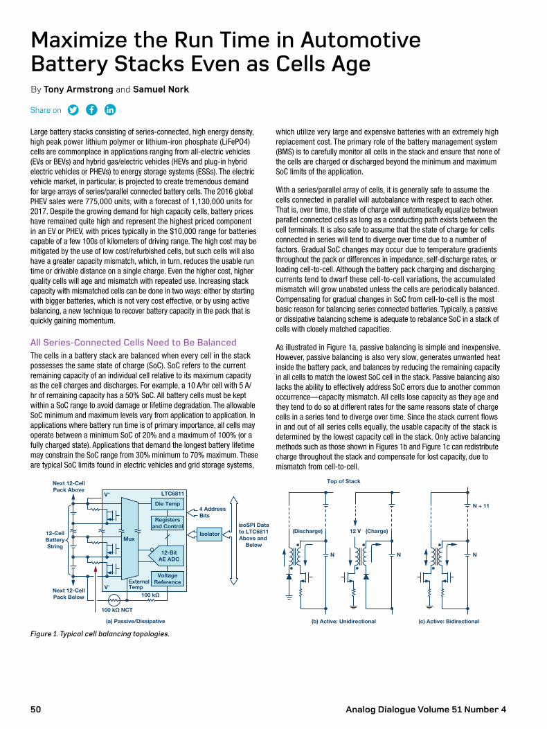
Analog Dialogue Volume 51 Number 450
Share on
which utilize very large and expensive batteries with an extremely high replacement cost. The primary role of the battery management system (BMS) is to carefully monitor all cells in the stack and ensure that none of the cells are charged or discharged beyond the minimum and maximum SoC limits of the application.
With a series/parallel array of cells, it is generally safe to assume the cells connected in parallel will autobalance with respect to each other. That is, over time, the state of charge will automatically equalize between parallel connected cells as long as a conducting path exists between the cell terminals. It is also safe to assume that the state of charge for cells connected in series will tend to diverge over time due to a number of factors. Gradual SoC changes may occur due to temperature gradients throughout the pack or differences in impedance, self-discharge rates, or loading cell-to-cell. Although the battery pack charging and discharging currents tend to dwarf these cell-to-cell variations, the accumulated mismatch will grow unabated unless the cells are periodically balanced. Compensating for gradual changes in SoC from cell-to-cell is the most basic reason for balancing series connected batteries. Typically, a passive or dissipative balancing scheme is adequate to rebalance SoC in a stack of cells with closely matched capacities.
As illustrated in Figure 1a, passive balancing is simple and inexpensive. However, passive balancing is also very slow, generates unwanted heat inside the battery pack, and balances by reducing the remaining capacity in all cells to match the lowest SoC cell in the stack. Passive balancing also lacks the ability to effectively address SoC errors due to another common occurrence—capacity mismatch. All cells lose capacity as they age and they tend to do so at different rates for the same reasons state of charge cells in a series tend to diverge over time. Since the stack current flows in and out of all series cells equally, the usable capacity of the stack is determined by the lowest capacity cell in the stack. Only active balancing methods such as those shown in Figures 1b and Figure 1c can redistribute charge throughout the stack and compensate for lost capacity, due to mismatch from cell-to-cell.
Large battery stacks consisting of series-connected, high energy density, high peak power lithium polymer or lithium-iron phosphate (LiFePO4) cells are commonplace in applications ranging from all-electric vehicles (EVs or BEVs) and hybrid gas/electric vehicles (HEVs and plug-in hybrid electric vehicles or PHEVs) to energy storage systems (ESSs). The electric vehicle market, in particular, is projected to create tremendous demand for large arrays of series/parallel connected battery cells. The 2016 global PHEV sales were 775,000 units, with a forecast of 1,130,000 units for 2017. Despite the growing demand for high capacity cells, battery prices have remained quite high and represent the highest priced component in an EV or PHEV, with prices typically in the $10,000 range for batteries capable of a few 100s of kilometers of driving range. The high cost may be mitigated by the use of low cost/refurbished cells, but such cells will also have a greater capacity mismatch, which, in turn, reduces the usable run time or drivable distance on a single charge. Even the higher cost, higher quality cells will age and mismatch with repeated use. Increasing stack capacity with mismatched cells can be done in two ways: either by starting with bigger batteries, which is not very cost effective, or by using active balancing, a new technique to recover battery capacity in the pack that is quickly gaining momentum.
All Series-Connected Cells Need to Be BalancedThe cells in a battery stack are balanced when every cell in the stack possesses the same state of charge (SoC). SoC refers to the current remaining capacity of an individual cell relative to its maximum capacity as the cell charges and discharges. For example, a 10 A/hr cell with 5 A/hr of remaining capacity has a 50% SoC. All battery cells must be kept within a SoC range to avoid damage or lifetime degradation. The allowable SoC minimum and maximum levels vary from application to application. In applications where battery run time is of primary importance, all cells may operate between a minimum SoC of 20% and a maximum of 100% (or a fully charged state). Applications that demand the longest battery lifetime may constrain the SoC range from 30% minimum to 70% maximum. These are typical SoC limits found in electric vehicles and grid storage systems,
Maximize the Run Time in Automotive Battery Stacks Even as Cells Age By Tony Armstrong and Samuel Nork
Next 12-CellPack Above
12-CellBatteryString
100 kΩ
100 kΩ NCT
(a) Passive/Dissipative
VoltageReferenceExternal
Temp
Isolator
isoSPI Datato LTC6811Above and
Below
Die Temp
LTC6811
4 AddressBits
Next 12-CellPack Below
V+
V–
Registersand Control
Mux
12-BitAE ADC
(b) Active: Unidirectional
N N
12 V (Charge)
Top of Stack
(Discharge)
(c) Active: Bidirectional
N
N + 11
Figure 1. Typical cell balancing topologies.

Analog Dialogue Volume 51 Number 4 51
Cell-to-Cell Mismatch Can Dramatically Reduce Run TimeCell-to-cell mismatch in either capacity or SoC may severely reduce the usable battery stack capacity unless the cells are balanced. Maximizing stack capacity requires that the cells are balanced both during stack charging, as well as stack discharging. In the example shown in Figure 2, a 10-cell series stack comprised of (nominal) 100 A/hr cells with a ±10% capacity error from the minimum capacity cell to the maximum is charged and discharged until predetermined SoC limits are reached. If SoC levels are constrained to between 30% and 70% and no balancing is performed, the usable stack capacity is reduced by 25% after a complete charge/discharge cycle relative to the theoretical usable capacity of the cells. Passive balancing could theoretically equalize each cell’s SoC during the stack charging phase, but could do nothing to prevent cell 10 from reaching its 30% SoC level before the others during discharge. Even with passive balancing during stack charging, significant capacity is lost (not usable) during stack discharge. Only an active balancing solution can achieve capacity recovery by redistributing charge from high SoC cells to low SoC cells during stack discharging.
Cell #12345678910
StackCapacity
Capacity(A/hr)11010010010010010010010010090
1000
InitialSoC(%)100100100100100100100100100100
Capacity(A/hr)
47373737373737373727
370
Post-Discharge
No Active Balancing (30% to 70% SoC Limits)
Usable Stack Capacity: 670 A/hr to 370 A/hr = 300 A/hr(75% of 400 A/hr Theoretical Max Capacity → 100 A/hr lost)
SoC(%)43373737373737373730
Capacity(A/hr)
77676767676767676757
670
Post-DischargeSoC(%)70676767676767676763
No Balance No Balance
Figure 2. Stack capacity loss example due to cell-to-cell mismatch.
Figure 3 illustrates how the use of ideal active balancing enables 100% recovery of the lost capacity due to cell-to-cell mismatch. During steady state use when the stack is discharging from its 70% SoC fully recharged state,
stored charge must in effect be taken from cell 1 (the highest capacity cell) and transferred to cell 10 (the lowest capacity cell)—otherwise cell 10 reaches its 30% minimum SoC point before the rest of the cells and the stack discharging must stop to prevent further lifetime degradation. Similarly, charge must be removed from cell 10 and redistributed to cell 1 during the charging phase—otherwise cell 10 reaches its 70% upper SoC limit first and the charging cycle must stop. At some point over the operating life of a battery stack, variations in cell aging will inevitably create cell-to-cell capacity mismatch. Only an active balancing solution can achieve capacity recovery by redistributing charge from high SoC cells to low SoC cells as needed. Achieving maximum battery stack capacity over the life of the battery stack requires an active balancing solution to efficiently charge and discharge individual cells to maintain SoC balance throughout the stack.
Cell #12345678910
StackCapacity
Capacity(A/hr)11010010010010010010010010090
1000
InitialSoC(%)100100100100100100100100100100
Capacity(A/hr)
33303030303030303027
370
Post-Discharge
100% Efficient (30% to 70% SoC Limits)
Usable Stack Capacity: 700 A/hr to 370 A/hr = 400 A/hr(100% of 400 A/hr Theoretical Max Capacity)
SoC(%)30303030303030303030
Capacity(A/hr)
77707070707070707063
700
Post-DischargeSoC(%)70707070707070707070
Active BalanceActive Balance
Figure 3. Capacity recovery due to ideal active balancing.
High Efficiency, Bidirectional Balancing Provides Highest Capacity RecoveryThe LTC3300-2 (see Figure 4) is a new product designed specifically to address the need for high performance active balancing. The LTC3300-2 is a high efficiency, bidirectional, active balance control IC that is a key piece of a high performance BMS system. Each IC can simultaneously balance up to six Li-Ion or LiFePO4 cells connected in series.
ICHARGEChargeSupply
ChargeReturn
ChargeReturn(IDISCHARGE1 to 6)
ChargeSupply
(ICHARGE1 to 6)
IDISCHARGE Cell 6
LTC3300-2
Address n
LTC3300-2
Address n + 1Cell 7
Cell 12
Cell 1
Next Cell Below
Next Cell Above
+
+
+
+
Isolator4
5
4
4
4Serial I/O
Isolator4
5
Figure 4. LTC3300-2 high efficiency, bidirectional, multicell active balancer.
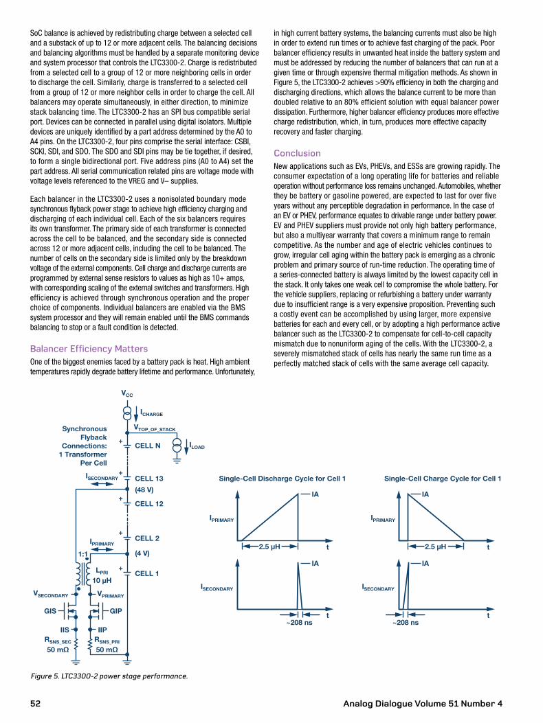
Analog Dialogue Volume 51 Number 452
SoC balance is achieved by redistributing charge between a selected cell and a substack of up to 12 or more adjacent cells. The balancing decisions and balancing algorithms must be handled by a separate monitoring device and system processor that controls the LTC3300-2. Charge is redistributed from a selected cell to a group of 12 or more neighboring cells in order to discharge the cell. Similarly, charge is transferred to a selected cell from a group of 12 or more neighbor cells in order to charge the cell. All balancers may operate simultaneously, in either direction, to minimize stack balancing time. The LTC3300-2 has an SPI bus compatible serial port. Devices can be connected in parallel using digital isolators. Multiple devices are uniquely identified by a part address determined by the A0 to A4 pins. On the LTC3300-2, four pins comprise the serial interface: CSBI, SCKI, SDI, and SDO. The SDO and SDI pins may be tie together, if desired, to form a single bidirectional port. Five address pins (A0 to A4) set the part address. All serial communication related pins are voltage mode with voltage levels referenced to the VREG and V– supplies.
Each balancer in the LTC3300-2 uses a nonisolated boundary mode synchronous flyback power stage to achieve high efficiency charging and discharging of each individual cell. Each of the six balancers requires its own transformer. The primary side of each transformer is connected across the cell to be balanced, and the secondary side is connected across 12 or more adjacent cells, including the cell to be balanced. The number of cells on the secondary side is limited only by the breakdown voltage of the external components. Cell charge and discharge currents are programmed by external sense resistors to values as high as 10+ amps, with corresponding scaling of the external switches and transformers. High efficiency is achieved through synchronous operation and the proper choice of components. Individual balancers are enabled via the BMS system processor and they will remain enabled until the BMS commands balancing to stop or a fault condition is detected.
Balancer Efficiency MattersOne of the biggest enemies faced by a battery pack is heat. High ambient temperatures rapidly degrade battery lifetime and performance. Unfortunately,
VCC
CELL N+
+
+
+
+
CELL 13
(48 V)
(4 V)
CELL 12
CELL 1
CELL 2
VTOP_OF_STACK
ICHARGE
ILOAD
ISECONDARY
ISECONDARYVSECONDARY
LPRI
10 µH
2.5 µH1:1
RSNS_PRI
50 mΩRSNS_SEC
50 mΩ
SynchronousFlyback
Connections:1 Transformer
Per Cell
IPRIMARY
IPRIMARY
IA
Single-Cell Discharge Cycle for Cell 1 Single-Cell Charge Cycle for Cell 1
VPRIMARY
GIPGIS
IIPIIS
ISECONDARY
IPRIMARY
IA
t t
t t
IA
IA
2.5 µH
~208 ns~208 ns
Figure 5. LTC3300-2 power stage performance.
in high current battery systems, the balancing currents must also be high in order to extend run times or to achieve fast charging of the pack. Poor balancer efficiency results in unwanted heat inside the battery system and must be addressed by reducing the number of balancers that can run at a given time or through expensive thermal mitigation methods. As shown in Figure 5, the LTC3300-2 achieves >90% efficiency in both the charging and discharging directions, which allows the balance current to be more than doubled relative to an 80% efficient solution with equal balancer power dissipation. Furthermore, higher balancer efficiency produces more effective charge redistribution, which, in turn, produces more effective capacity recovery and faster charging.
ConclusionNew applications such as EVs, PHEVs, and ESSs are growing rapidly. The consumer expectation of a long operating life for batteries and reliable operation without performance loss remains unchanged. Automobiles, whether they be battery or gasoline powered, are expected to last for over five years without any perceptible degradation in performance. In the case of an EV or PHEV, performance equates to drivable range under battery power. EV and PHEV suppliers must provide not only high battery performance, but also a multiyear warranty that covers a minimum range to remain competitive. As the number and age of electric vehicles continues to grow, irregular cell aging within the battery pack is emerging as a chronic problem and primary source of run-time reduction. The operating time of a series-connected battery is always limited by the lowest capacity cell in the stack. It only takes one weak cell to compromise the whole battery. For the vehicle suppliers, replacing or refurbishing a battery under warranty due to insufficient range is a very expensive proposition. Preventing such a costly event can be accomplished by using larger, more expensive batteries for each and every cell, or by adopting a high performance active balancer such as the LTC3300-2 to compensate for cell-to-cell capacity mismatch due to nonuniform aging of the cells. With the LTC3300-2, a severely mismatched stack of cells has nearly the same run time as a perfectly matched stack of cells with the same average cell capacity.
Analog Dialogue Volume 51 Number 4 53
Sam Nork [[email protected]] joined Linear Technology, now a part of Analog Devices, as a senior product engineer at the company’s Milpitas, CA headquarters in 1988. In 1994, he relocated to the Boston area to start up and manage an analog IC design center, where he continues to work today. Sam has personally designed and released numerous integrated circuits in the area of portable power management, and is inventor/co-inventor on seven issued patents. As director of Analog Devices’ Boston design center, Sam leads a team of nearly 100 people and oversees the day-to-day development activity for a wide variety of analog integrated circuits in areas including portable power management, high speed op amps, industrial ADCs, system monitors, and energy harvesting. Prior to his role at the design center, Sam worked for Analog Devices in Wilmington, MA as a product/test development engineer. He received A.B. and B.E. degrees from Dartmouth College.
Samuel Nork
Tony Armstrong [[email protected]], marketing director of power products, joined the company in May of 2000. He is responsible for all aspects of the power conversion and management products from conception through obsolescence. Prior to joining Analog Devices, Tony held various positions in marketing, sales, and operations at Siliconix Inc., Semtech Corp., Fairchild Semiconductors, and Intel Corp. in Europe. He attained a B.S. (honors) in applied mathematics from the University of Manchester, England in 1981.
Tony Armstrong

Analog Dialogue Volume 51 Number 454
Typical Drain Pulse ConfigurationA typical configuration for HPA turn on/off through drain control is shown in Figure 1. A series FET turns on the high voltage to the HPA. The control circuit is required to convert a logic-level pulse to a higher voltage to turn on the series FET.
Complications of this configuration include:
X The switching of large currents requires a low inductance path from the bulk storage capacitance to the drain pin of the HPA.
X At turn off, the drain capacitance maintains a charge and needs an additional discharge path. This is accomplished with an additional FET Q2, which adds a constraint on the control circuit that Q1 and Q2 never be simultaneously enabled.
X In many cases, the series FET is an N-Channel device. This requires the control circuitry to produce a voltage higher than the HPA drain voltage for turn on.
The design approaches for the control circuitry are well known and proven. However, the continued desire for integrated packaging and reduced SWaP in phased array systems lead to a desire to eliminate this complication. In fact, the desire is to eliminate the drain control circuit entirely.
Bulk Capacitance
Logic Input
HPA
Pulsed Drain
Q2
Q1VDD
(28 V to 50 V Typical)
ControlCircuitry
RFIN RFOUT
VGATE
Figure 1. Traditional HPA pulsed drain configuration.
Question:Can you switch on or off your RF source within 200 ns?
Answer:In pulsed radar applications, rapid turn on/off of the high power amplifier (HPA) is required during the transition from transmit to receive operation. Typical transition time objectives can be less than 1 µs. Historically this has been implemented through drain control. Drain control necessitates switching large currents at voltages ranging from 28 V to 50 V. This is practical with known switching power techniques, but involves additional physical size and circuit complications. In modern phased array antenna developments, while demanding the lowest SWaP possible, it is desirable to eliminate the complications associated with drain switching on HPAs.
This article presents a unique, yet simple gate pulse drive circuit that provides an alternate method for fast HPA turn on/off and eliminates the circuitry involved with drain switching. Measured switching times are less than 200 ns, providing margin against a 1 µs objective. Additional features include bias programmability to account for part-to-part variation, a gate clamp protecting the HPA from an unintended gate voltage increase, and an overshoot compensation for pulse rise time optimization.
Rarely Asked Questions—Issue 148Unique Gate Drive Applications Enable Rapidly Switching On/Off for Your High Power AmplifierBy Peter Delos and Jarrett Liner
Share on
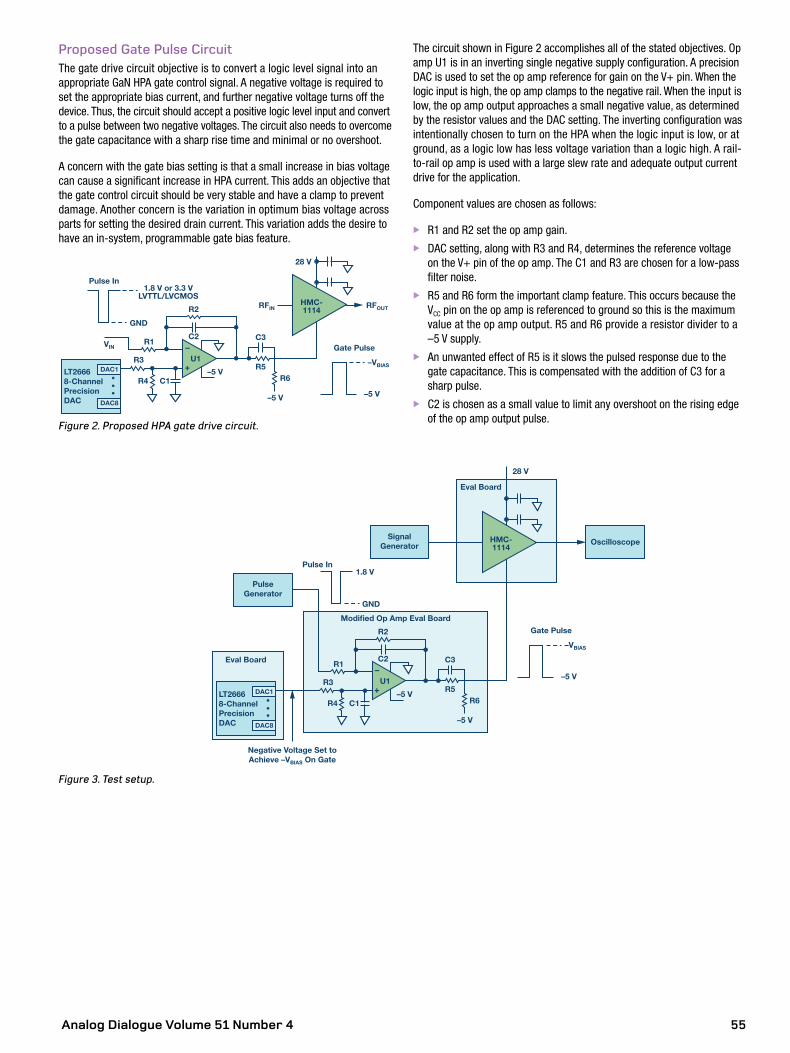
Analog Dialogue Volume 51 Number 4 55
Proposed Gate Pulse CircuitThe gate drive circuit objective is to convert a logic level signal into an appropriate GaN HPA gate control signal. A negative voltage is required to set the appropriate bias current, and further negative voltage turns off the device. Thus, the circuit should accept a positive logic level input and convert to a pulse between two negative voltages. The circuit also needs to overcome the gate capacitance with a sharp rise time and minimal or no overshoot.
A concern with the gate bias setting is that a small increase in bias voltage can cause a significant increase in HPA current. This adds an objective that the gate control circuit should be very stable and have a clamp to prevent damage. Another concern is the variation in optimum bias voltage across parts for setting the desired drain current. This variation adds the desire to have an in-system, programmable gate bias feature.
RFIN
VIN
GND
1.8 V or 3.3 VLVTTL/LVCMOS
–5 V–5 V
–5 VLT26668-ChannelPrecisionDAC
C3C2
R2
R1
R3
R4 C1
R5R6
28 V
–VBIAS
HMC-1114
RFOUT
Gate Pulse
Pulse In
DAC1
DAC8
U1
Figure 2. Proposed HPA gate drive circuit.
The circuit shown in Figure 2 accomplishes all of the stated objectives. Op amp U1 is in an inverting single negative supply configuration. A precision DAC is used to set the op amp reference for gain on the V+ pin. When the logic input is high, the op amp clamps to the negative rail. When the input is low, the op amp output approaches a small negative value, as determined by the resistor values and the DAC setting. The inverting configuration was intentionally chosen to turn on the HPA when the logic input is low, or at ground, as a logic low has less voltage variation than a logic high. A rail-to-rail op amp is used with a large slew rate and adequate output current drive for the application.
Component values are chosen as follows:
X R1 and R2 set the op amp gain. X DAC setting, along with R3 and R4, determines the reference voltage
on the V+ pin of the op amp. The C1 and R3 are chosen for a low-pass filter noise.
X R5 and R6 form the important clamp feature. This occurs because the VCC pin on the op amp is referenced to ground so this is the maximum value at the op amp output. R5 and R6 provide a resistor divider to a –5 V supply.
X An unwanted effect of R5 is it slows the pulsed response due to the gate capacitance. This is compensated with the addition of C3 for a sharp pulse.
X C2 is chosen as a small value to limit any overshoot on the rising edge of the op amp output pulse.
GND
1.8 V
–5 V
–5 V
–5 VLT26668-ChannelPrecisionDAC
C3C2
R2
R1
R3
R4 C1
R5R6
28 V
–VBIAS
HMC-1114
Gate Pulse
Pulse In
PulseGenerator
SignalGenerator Oscilloscope
Eval Board
Negative Voltage Set toAchieve –VBIAS On Gate
Eval Board
Modified Op Amp Eval Board
DAC1
DAC8
U1
Figure 3. Test setup.
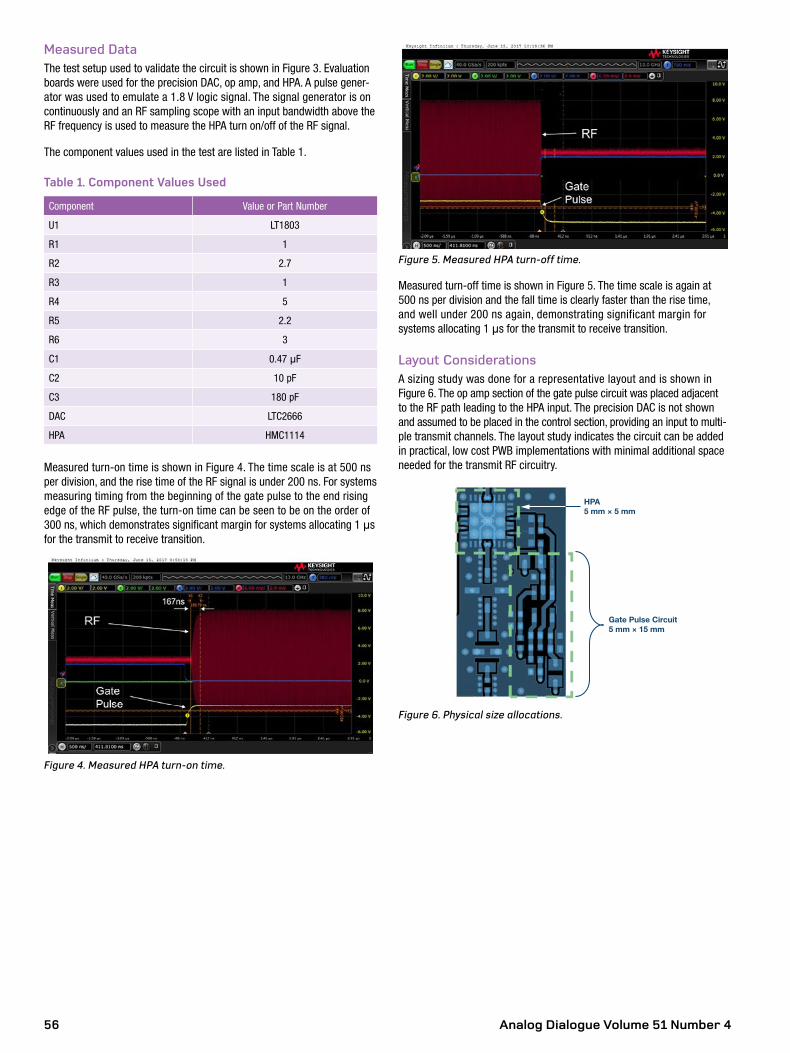
Analog Dialogue Volume 51 Number 456
Measured DataThe test setup used to validate the circuit is shown in Figure 3. Evaluation boards were used for the precision DAC, op amp, and HPA. A pulse gener-ator was used to emulate a 1.8 V logic signal. The signal generator is on continuously and an RF sampling scope with an input bandwidth above the RF frequency is used to measure the HPA turn on/off of the RF signal.
The component values used in the test are listed in Table 1.
Table 1. Component Values Used
Component Value or Part Number
U1 LT1803
R1 1
R2 2.7
R3 1
R4 5
R5 2.2
R6 3
C1 0.47 µF
C2 10 pF
C3 180 pF
DAC LTC2666
HPA HMC1114
Measured turn-on time is shown in Figure 4. The time scale is at 500 ns per division, and the rise time of the RF signal is under 200 ns. For systems measuring timing from the beginning of the gate pulse to the end rising edge of the RF pulse, the turn-on time can be seen to be on the order of 300 ns, which demonstrates significant margin for systems allocating 1 μs for the transmit to receive transition.
Figure 4. Measured HPA turn-on time.
Figure 5. Measured HPA turn-off time.
Measured turn-off time is shown in Figure 5. The time scale is again at 500 ns per division and the fall time is clearly faster than the rise time, and well under 200 ns again, demonstrating significant margin for systems allocating 1 μs for the transmit to receive transition.
Layout ConsiderationsA sizing study was done for a representative layout and is shown in Figure 6. The op amp section of the gate pulse circuit was placed adjacent to the RF path leading to the HPA input. The precision DAC is not shown and assumed to be placed in the control section, providing an input to multi-ple transmit channels. The layout study indicates the circuit can be added in practical, low cost PWB implementations with minimal additional space needed for the transmit RF circuitry.
HPA5 mm × 5 mm
Gate Pulse Circuit5 mm × 15 mm
Figure 6. Physical size allocations.

Analog Dialogue Volume 51 Number 4 57
Also by this Author:
Improved DAC Phase Noise Measurements Enable Ultralow Phase Noise DDS Applications
Volume 51, Number 3
Also by this Author:
Improved DAC Phase Noise Measurements Enable Ultralow Phase Noise DDS Applications
Volume 51, Number 3
Jarrett Liner [ [email protected]] is an RF systems application engineer with Analog Devices, Inc., in the Aerospace and Defense Group in Greensboro, NC. He has significant experience in the area of RF system and component design.
Formerly, Jarrett was an applications engineer for GaN on SiC amplifiers for the military and aerospace sector. His prior experience also includes design and test of RF IC WLAN power amplifier and front-end modules for 13 years. He served 6 years in the United States Navy as an electronics technician. Jarrett received his B.S.E.E. from North Carolina Agricultural and Technical State University located in Greensboro, NC, in 2004.
When Jarrett isn’t simulating circuit solutions or taking data in the lab, he might be found mountain biking, teaching cycle class at the gym, running, or chasing his four kids around the yard.
Jarett Liner
Peter Delos [[email protected]] is a technical lead at Analog Devices in the Aerospace and Defense Group. He received his B.S.E.E. from Virginia Tech in 1990 and M.S.E.E. from NJIT in 2004. He worked in the Naval Nuclear Power program from 1990 to 1997. This work included completion of the Naval Nuclear Power School Officer’s Program, and work as an instructor in a Naval submarine facility and as a lead electrical field engineer on the Seawolf-class submarines in Groton, CT.
In 1997, he accepted a position with Lockheed Martin in Moorestown, NJ, and began a prolific career developing receivers/exciters and synthesizers for multiple radar and EW programs. This experience encompassed architecture definition, detailed design, rapid prototypes, manufacturing coverage, field installations, and coordination, among many engineering disciplines. This work led the migration of phased array receiver/exciter electronics from central-ized architectures to on-array digital beamforming systems.
In 2016, he accepted a position with Analog Devices in Greensboro, NC. He has nearly 20 years of experience in RF systems designing at the architec-ture level, PWB level, and IC level.
Peter Delos
SummaryA unique gate pulse circuit has been presented and evaluated for rapid HPA turn on/off.
Features include:
X <200 ns transition times. X Compatibility with any logic input. X Programmable bias for part-to-part variation.
X Clamp protection provided to set a maximum gate voltage. X Rise time/overshoot compensation. X Size supports high density phased array applications.
With the continued integration of advanced electronic systems demanding reduced physical footprints, it is envisioned that this circuit, and variations of its approach, will begin to proliferate in phased array applications requiring rapid HPA transition times.

Analog Dialogue Volume 51 Number 458
Notes

Analog Dialogue Volume 51 Number 4 59
Notes

EngineerZone® Support CommunityEngage with the ADI technology experts in the community to ask your toughdesign questions, browse our rich knowledge base, or hear from our authorsin the Analog Dialogue blog. ez.analog.com, ezchina.analog.com (China)
Stay Connected with Analog Dialogue
twitter.com/ADI_News
facebook.com/AnalogDevicesInc
WeChat (China)
linkedin.com/company/analog-devices
weibo.com/analogdevices
Your Engineering Resource for Innovative DesignBe the first to receive the latest technology, applications, and systems-levelinsights needed to solve real-world design challenges by subscribing toAnalog Dialogue. And be sure to tell a friend! analogdialogue.com
Facebook @ADI_News LinkedIn Sina Weibo (China)
Like Analog Dialogue to discover the latest articles and author insights.facebook.com/analogdialogue
Analog Devices, Inc. Worldwide Headquarters
Analog Devices, Inc. One Technology Way P.O. Box 9106 Norwood, MA 02062-9106 U.S.A. Tel: 781.329.4700 (800.262.5643, U.S.A. only) Fax: 781.461.3113
Analog Devices, Inc. Europe Headquarters
Analog Devices GmbH Otl-Aicher-Str. 60-6480807 München Germany Tel: 49.89.76903.0 Fax: 49.89.76903.157
Analog Devices, Inc. Japan Headquarters
Analog Devices, KK New Pier Takeshiba South Tower Building 1-16-1 Kaigan, Minato-ku, Tokyo, 105-6891 Japan Tel: 813.5402.8200 Fax: 813.5402.1064
Analog Devices, Inc. Asia Pacific Headquarters
Analog Devices 5F, Sandhill Plaza 2290 Zuchongzhi Road Zhangjiang Hi-Tech Park Pudong New District Shanghai, China 201203 Tel: 86.21.2320.8000 Fax: 86.21.2320.8222
©2018 Analog Devices, Inc. All rights reserved. Trademarks and registered trademarks are the property of their respective owners.Ahead of What’s Possible is a trademark of Analog Devices.M02000-0-1/18
analog.com