8752c network analyzer service guide - silicon … · service guide agilent technologies 8752c...
TRANSCRIPT

Service Guide
Agilent Technologies8752C
Network Analyzer
Silicon Investigations
Repair Information - Contact Us
920-955-3693
www.siliconinvestigations.com
Manufacturing Part Number: 08752-90136
Printed in USA
Print Date: February 1998Supersedes: December 1997
© Agilent Technologies, Inc. 1998

Hewlett-Packard to Agilent Technologies TransitionThis manual may contain references to HP or Hewlett-Packard. Please note that Hewlett-Packard's former test and measurement, semiconductor products and chemical analysis businesses are now part of Agilent Technologies. To reduce potential confusion, the only change to product numbers and names has been in the company name prefix: where a product number/name was HP XXXX the current name/number is now Agilent XXXX. For example, model number HP 8752C is now model number Agilent 8752C.
Documentation WarrantyTHE MATERIAL CONTAINED IN THIS DOCUMENT IS PROVIDED "AS IS," AND IS SUBJECT TO BEING CHANGED, WITHOUT NOTICE, IN FUTURE EDITIONS. FUR-THER, TO THE MAXIMUM EXTENT PERMITTED BY APPLICABLE LAW, AGILENT DISCLAIMS ALL WARRANTIES, EITHER EXPRESS OR IMPLIED WITH REGARD TO THIS MANUAL AND ANY INFORMATION CONTAINED HEREIN, INCLUDING BUT NOT LIMITED TO THE IMPLIED WARRANTIES OF MERCHANTABILITY AND FIT-NESS FOR A PARTICULAR PURPOSE. AGILENT SHALL NOT BE LIABLE FOR ERRORS OR FOR INCIDENTAL OR CONSEQUENTIAL DAMAGES IN CONNECTION WITH THE FURNISHING, USE, OR PERFORMANCE OF THIS DOCUMENT OR ANY INFORMATION CONTAINED HEREIN. SHOULD AGILENT AND THE USER HAVE A SEPARATE WRITTEN AGREEMENT WITH WARRANTY TERMS COVERING THE MATERIAL IN THIS DOCUMENT THAT CONFLICT WITH THESE TERMS, THE WAR-RANTY TERMS IN THE SEPARATE AGREEMENT WILL CONTROL.
DFARS/Restricted Rights NoticeIf software is for use in the performance of a U.S. Government prime contract or subcontract, Software is delivered and licensed as “Commercial computer software” as defined in DFAR 252.227-7014 (June 1995), or as a “commercial item” as defined in FAR 2.101(a) or as “Restricted computer software” as defined in FAR 52.227-19 (June 1987) or any equivalent agency regulation or contract clause. Use, duplication or disclosure of Software is subject to Agilent Technologies’ standard commercial license terms, and non-DOD Departments and Agencies of the U.S. Government will receive no greater than Restricted Rights as defined in FAR 52.227-19(c)(1-2) (June 1987). U.S. Government users will receive no greater than Limited Rights as defined in FAR 52.227-14 (June 1987) or DFAR 252.227-7015 (b)(2) (November 1995), as applicable in any technical data.
Printing Copies of Documentation from the WebTo print copies of documentation from the Web, download the PDF file from the Agilent web site:
• Go to http://www.agilent.com.
• Enter the document’s part number (located on the title page) in the Quick Search box.
• Click GO.
• Click on the hyperlink for the document.
• Click the printer icon located in the tool bar.

Contacting AgilentThis information supersedes all prior HP contact information.
Online assistance: www.agilent.com/find/assist
Americas
Brazil(tel) (+55) 11 3351 7012(fax) (+55) 11 3351 7024
Canada(tel) +1 877 894 4414(fax) +1 303 662 3369
Mexico(tel) 1 800 254 2440(fax) 1 800 254 4222
United States(tel) 800 829 4444(alt) (+1) 303 662 3998(fax) 800 829 4433
Asia Pacific and Japan
Australia(tel) 1 800 225 574(fax) 1 800 681 776(fax) 1 800 225 539
China(tel) 800 810 0508(alt) 800 810 0510(fax) 800 810 0507(fax) 800 810 0362
Hong Kong(tel) 800 933 229(fax) 800 900 701
India(tel) 1600 112 626(fax) 1600 112 727(fax) 1600 113 040
Japan (Bench)(tel) 0120 32 0119(alt) (+81) 426 56 7799(fax) 0120 01 2144
Japan (On-Site)(tel) 0120 802 363(alt) (+81) 426 56 7498(fax) (+81) 426 60 8953
Singapore(tel) 1 800 275 0880(fax) (+65) 6755 1235(fax) (+65) 6755 1214
South Korea(tel) 080 778 0011(fax) 080 778 0013
Taiwan(tel) 0800 047 669(fax) 0800 047 667(fax) 886 3492 0779
Thailand(tel) 1 800 2758 5822(alt) (+66) 2267 5913(fax) 1 800 656 336
Malaysia(tel) 1800 880 399(fax) 1800 801 054
Europe
Austria(tel) 0820 87 44 11*(fax) 0820 87 44 22
Belgium(tel) (+32) (0)2 404 9340(alt) (+32) (0)2 404 9000(fax) (+32) (0)2 404 9395
Denmark(tel) (+45) 7013 1515(alt) (+45) 7013 7313(fax) (+45) 7013 1555
Finland(tel) (+358) 10 855 2100(fax) (+358) (0) 10 855 2923
France(tel) 0825 010 700*(alt) (+33) (0)1 6453 5623(fax) 0825 010 701*
Germany(tel) 01805 24 6333*(alt) 01805 24 6330*(fax) 01805 24 6336*
Ireland(tel) (+353) (0)1 890 924 204(alt) (+353) (0)1 890 924 206(fax)(+353) (0)1 890 924 024
Israel(tel) (+972) 3 9288 500(fax) (+972) 3 9288 501
Italy(tel) (+39) (0)2 9260 8484(fax) (+39) (0)2 9544 1175
Luxemburg(tel) (+32) (0)2 404 9340(alt) (+32) (0)2 404 9000(fax) (+32) (0)2 404 9395
Netherlands(tel) (+31) (0)20 547 2111(alt) (+31) (0)20 547 2000(fax) (+31) (0)20 547 2190
Russia(tel) (+7) 095 797 3963(alt) (+7) 095 797 3900(fax) (+7) 095 797 3901
Spain(tel) (+34) 91 631 3300(alt) (+34) 91 631 3000(fax) (+34) 91 631 3301
Sweden(tel) 0200 88 22 55*(alt) (+46) (0)8 5064 8686(fax) 020 120 2266*
Switzerland (French)(tel) 0800 80 5353 opt. 2*(alt) (+33) (0)1 6453 5623(fax) (+41) (0)22 567 5313
Switzerland (German)(tel) 0800 80 5353 opt. 1*(alt) (+49) (0)7031 464 6333(fax) (+41) (0)1 272 7373
Switzerland (Italian)(tel) 0800 80 5353 opt. 3*(alt) (+39) (0)2 9260 8484(fax) (+41) (0)22 567 5314
United Kingdom(tel) (+44) (0)7004 666666(alt) (+44) (0)7004 123123(fax) (+44) (0)7004 444555
(tel) = primary telephone number; (alt) = alternate telephone number; (fax) = FAX number; * = in country number 11/16/04

Service Guide
HP 8752C Network Analyzer
ABCDE
HP Part No. 08752-90136 Supersedes December 1997
Printed in USA February 1998

Notice.The information contained in this document is subject to change without notice.
Hewlett-Packard makes no warranty of any kind with regard to this material,including but not limited to, the implied warranties of merchantability and�tness for a particular purpose. Hewlett-Packard shall not be liable for errorscontained herein or for incidental or consequential damages in connection withthe furnishing, performance, or use of this material.
c Copyright 1995, 1997, 1998 Hewlett-Packard Company

Contents
1. Service Equipment and Analyzer OptionsTable of Service Test Equipment . . . . . . . . . . . . . . . . 1-1Principles of Microwave Connector Care . . . . . . . . . . . . 1-5Analyzer Options Available . . . . . . . . . . . . . . . . . . . 1-7Option 003, 3 GHz Operation . . . . . . . . . . . . . . . . . 1-7
Option 004, Step Attenuator . . . . . . . . . . . . . . . . . 1-7
Option 006, 6 GHz Operation . . . . . . . . . . . . . . . . . 1-7
Option 010, Time Domain . . . . . . . . . . . . . . . . . . 1-7
Option 075, 75 Impedance . . . . . . . . . . . . . . . . . . 1-7
Option 1CM, Rack Mount Flange Kit Without Handles . . . . . 1-7Option 1CP, Rack Mount Flange Kit With Handles . . . . . . . 1-8
Option AFN, add 50 Test Port Cable . . . . . . . . . . . . . 1-8
Option AFP, add 75 Test Port Cable . . . . . . . . . . . . . 1-8
Option B02, External Disk Drive . . . . . . . . . . . . . . . 1-8
Service and Support Options . . . . . . . . . . . . . . . . . . 1-9
2. System Veri�cation and Performance Tests
How to Test the Performance of Your Analyzer . . . . . . . . . 2-1
Sections in this Chapter . . . . . . . . . . . . . . . . . . . . 2-2
HP 8752C System Veri�cation . . . . . . . . . . . . . . . . . . 2-3Equipment . . . . . . . . . . . . . . . . . . . . . . . . . 2-3
Description . . . . . . . . . . . . . . . . . . . . . . . . . 2-3System Veri�cation Cycle and Kit Recerti�cation . . . . . . . . 2-4Measurement Uncertainty . . . . . . . . . . . . . . . . . . 2-4
Measurement Uncertainty Window . . . . . . . . . . . . . . 2-4HP 8752C Type-N Test Port Characteristics (50 System) . . . . 2-6
Directivity . . . . . . . . . . . . . . . . . . . . . . . . 2-6
Source Match (Re ection) . . . . . . . . . . . . . . . . . 2-6
Source Match (Transmission)* . . . . . . . . . . . . . . . 2-6
Re ection Tracking . . . . . . . . . . . . . . . . . . . . 2-6
Load Match . . . . . . . . . . . . . . . . . . . . . . . . 2-7Transmission Tracking . . . . . . . . . . . . . . . . . . . 2-7
Contents-1
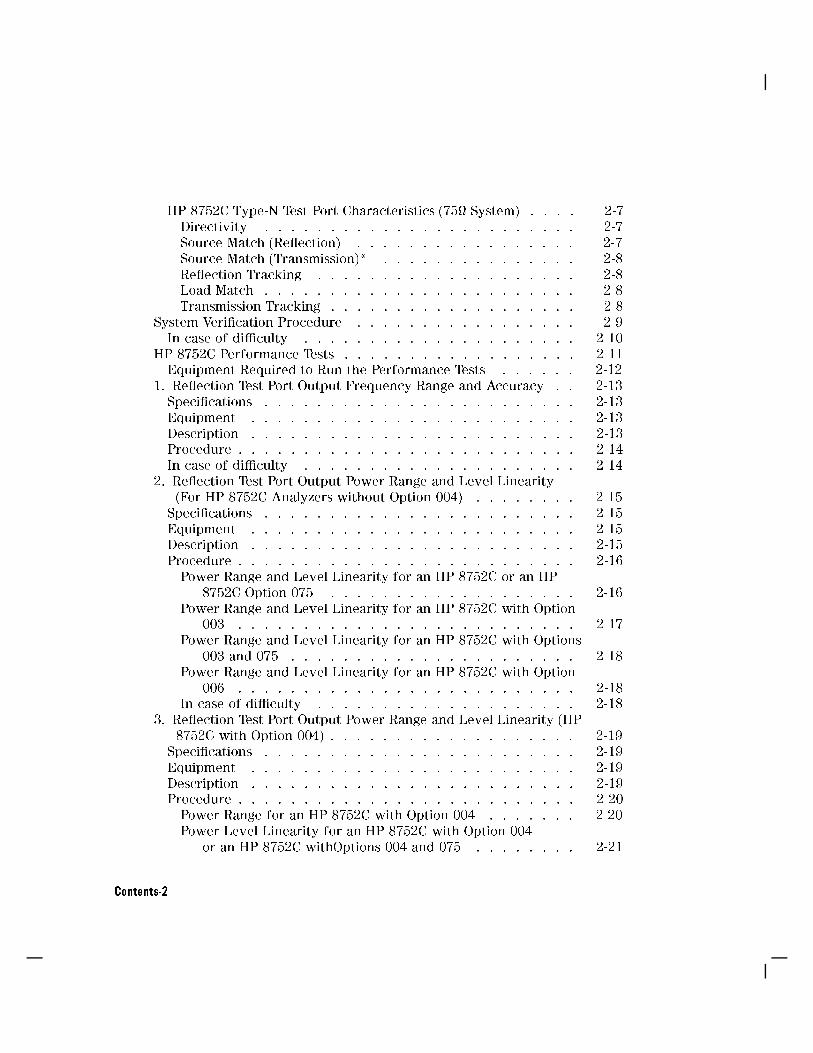
HP 8752C Type-N Test Port Characteristics (75 System) . . . . 2-7Directivity . . . . . . . . . . . . . . . . . . . . . . . . 2-7Source Match (Re ection) . . . . . . . . . . . . . . . . . 2-7Source Match (Transmission)* . . . . . . . . . . . . . . . 2-8Re ection Tracking . . . . . . . . . . . . . . . . . . . . 2-8Load Match . . . . . . . . . . . . . . . . . . . . . . . . 2-8Transmission Tracking . . . . . . . . . . . . . . . . . . . 2-8
System Veri�cation Procedure . . . . . . . . . . . . . . . . . 2-9
In case of di�culty . . . . . . . . . . . . . . . . . . . . . 2-10HP 8752C Performance Tests . . . . . . . . . . . . . . . . . . 2-11Equipment Required to Run the Performance Tests . . . . . . 2-12
1. Re ection Test Port Output Frequency Range and Accuracy . . 2-13Speci�cations . . . . . . . . . . . . . . . . . . . . . . . . 2-13
Equipment . . . . . . . . . . . . . . . . . . . . . . . . . 2-13
Description . . . . . . . . . . . . . . . . . . . . . . . . . 2-13Procedure . . . . . . . . . . . . . . . . . . . . . . . . . . 2-14
In case of di�culty . . . . . . . . . . . . . . . . . . . . . 2-14
2. Re ection Test Port Output Power Range and Level Linearity
(For HP 8752C Analyzers without Option 004) . . . . . . . . 2-15
Speci�cations . . . . . . . . . . . . . . . . . . . . . . . . 2-15
Equipment . . . . . . . . . . . . . . . . . . . . . . . . . 2-15Description . . . . . . . . . . . . . . . . . . . . . . . . . 2-15
Procedure . . . . . . . . . . . . . . . . . . . . . . . . . . 2-16
Power Range and Level Linearity for an HP 8752C or an HP
8752C Option 075 . . . . . . . . . . . . . . . . . . . 2-16
Power Range and Level Linearity for an HP 8752C with Option003 . . . . . . . . . . . . . . . . . . . . . . . . . . 2-17
Power Range and Level Linearity for an HP 8752C with Options
003 and 075 . . . . . . . . . . . . . . . . . . . . . . 2-18Power Range and Level Linearity for an HP 8752C with Option
006 . . . . . . . . . . . . . . . . . . . . . . . . . . 2-18In case of di�culty . . . . . . . . . . . . . . . . . . . . 2-18
3. Re ection Test Port Output Power Range and Level Linearity (HP8752C with Option 004) . . . . . . . . . . . . . . . . . . . 2-19
Speci�cations . . . . . . . . . . . . . . . . . . . . . . . . 2-19
Equipment . . . . . . . . . . . . . . . . . . . . . . . . . 2-19
Description . . . . . . . . . . . . . . . . . . . . . . . . . 2-19Procedure . . . . . . . . . . . . . . . . . . . . . . . . . . 2-20
Power Range for an HP 8752C with Option 004 . . . . . . . 2-20
Power Level Linearity for an HP 8752C with Option 004or an HP 8752C withOptions 004 and 075 . . . . . . . . 2-21
Contents-2

Power Level Linearity for an HP 8752C with Options 003 and004 . . . . . . . . . . . . . . . . . . . . . . . . . . 2-22
Power Level Linearity for an HP 8752C with Options 004 and006 . . . . . . . . . . . . . . . . . . . . . . . . . . 2-23
Power Level Linearity for an HP 8752C with Options 003, 004,and 075 . . . . . . . . . . . . . . . . . . . . . . . . 2-23
In case of di�culty . . . . . . . . . . . . . . . . . . . . 2-234. Transmission Test Port Input Noise Floor Level (HP 8752C
without Option 075) . . . . . . . . . . . . . . . . . . . . 2-24Speci�cations . . . . . . . . . . . . . . . . . . . . . . . . 2-24Equipment . . . . . . . . . . . . . . . . . . . . . . . . . 2-24Description . . . . . . . . . . . . . . . . . . . . . . . . . 2-24Procedure . . . . . . . . . . . . . . . . . . . . . . . . . . 2-24
Noise Floor Level at 300 kHz to 1.3 GHz (Standard Option), 300kHz to 3 GHz (Option 003), or 300 kHz to 6 GHz (Option006) with an IF BW of 3 kHz . . . . . . . . . . . . . . 2-24
Noise Floor Level at 300 kHz to 1.3 GHz (Standard Option) or300 kHz to 3 GHz (Option 003) with an IF BW of 10 Hz . . 2-26
Noise Floor Level at 3 GHz to 6 GHz (Option 006) with an IFBW of 10 Hz . . . . . . . . . . . . . . . . . . . . . . 2-27
Noise Floor Level at 3 GHz to 6 GHz (Option 006) with IF BW of3 kHz . . . . . . . . . . . . . . . . . . . . . . . . . 2-28
In case of di�culty . . . . . . . . . . . . . . . . . . . . 2-28
5. Transmission Test Port Input Noise Floor Level
(HP 8752C with Option 075) . . . . . . . . . . . . . . . . . 2-29
Speci�cations . . . . . . . . . . . . . . . . . . . . . . . . 2-29Equipment . . . . . . . . . . . . . . . . . . . . . . . . . 2-29
Description . . . . . . . . . . . . . . . . . . . . . . . . . 2-29
Procedure . . . . . . . . . . . . . . . . . . . . . . . . . . 2-29Noise Floor Level at 300 kHz to 1.3 GHz (Option 075) or 300
kHz to3 GHz (Options 075 and 003) with an IF BW of 3 kHz 2-29Noise Floor Level at 300 kHz to 1.3 GHz (Option 075) or 300
kHz to3 GHz (Options 075 and 003) with an IF BW of 10 Hz 2-31In case of di�culty . . . . . . . . . . . . . . . . . . . . 2-31
6. Test Port Crosstalk . . . . . . . . . . . . . . . . . . . . . 2-32
Speci�cations . . . . . . . . . . . . . . . . . . . . . . . . 2-32
Equipment . . . . . . . . . . . . . . . . . . . . . . . . . 2-32Description . . . . . . . . . . . . . . . . . . . . . . . . . 2-32
Procedure . . . . . . . . . . . . . . . . . . . . . . . . . . 2-33
Test Port Crosstalk for a Standard HP 8752C or an HP 8752Cwith Option 003 . . . . . . . . . . . . . . . . . . . . 2-33
Contents-3

Test Port Crosstalk for an HP 8752C with Option 006 . . . . . 2-33Test Port Crosstalk for an HP 8752C with Option 075 . . . . . 2-34Test Port Crosstalk for an HP 8752C with Options 003 and 075 2-34In case of di�culty . . . . . . . . . . . . . . . . . . . . 2-35
7. System Trace Noise . . . . . . . . . . . . . . . . . . . . . 2-36Speci�cations . . . . . . . . . . . . . . . . . . . . . . . . 2-36Equipment . . . . . . . . . . . . . . . . . . . . . . . . . 2-36Description . . . . . . . . . . . . . . . . . . . . . . . . . 2-36
Procedure . . . . . . . . . . . . . . . . . . . . . . . . . . 2-37Re ection Trace Noise (Magnitude) . . . . . . . . . . . . . 2-37Re ection Trace Noise (Phase) . . . . . . . . . . . . . . . 2-38Transmission Trace Noise (Magnitude) . . . . . . . . . . . . 2-38Transmission Trace Noise (Phase) . . . . . . . . . . . . . . 2-39
In case of di�culty . . . . . . . . . . . . . . . . . . . . 2-39
8. Magnitude Dynamic Accuracy (HP 8752C - All Options) . . . . 2-40Speci�cations . . . . . . . . . . . . . . . . . . . . . . . . 2-40
Equipment . . . . . . . . . . . . . . . . . . . . . . . . . 2-40
Description . . . . . . . . . . . . . . . . . . . . . . . . . 2-41
Procedure . . . . . . . . . . . . . . . . . . . . . . . . . . 2-41
In case of di�culty . . . . . . . . . . . . . . . . . . . . 2-44
9. Phase Dynamic Accuracy (HP 8752C - All Options) . . . . . . 2-45Speci�cations . . . . . . . . . . . . . . . . . . . . . . . . 2-45
Equipment . . . . . . . . . . . . . . . . . . . . . . . . . 2-45
Description . . . . . . . . . . . . . . . . . . . . . . . . . 2-45
Procedure . . . . . . . . . . . . . . . . . . . . . . . . . . 2-46
10. Compression . . . . . . . . . . . . . . . . . . . . . . . . 2-47Speci�cations . . . . . . . . . . . . . . . . . . . . . . . . 2-47
Equipment . . . . . . . . . . . . . . . . . . . . . . . . . 2-47
Description . . . . . . . . . . . . . . . . . . . . . . . . . 2-47Procedure . . . . . . . . . . . . . . . . . . . . . . . . . . 2-48In case of di�culty . . . . . . . . . . . . . . . . . . . . 2-49
Performance Test Record . . . . . . . . . . . . . . . . . . . . 2-50
3. Adjustments and Correction Constants
When to Perform the Adjustment Procedures . . . . . . . . . . 3-1
Keep Correction Constants Current to Save Time . . . . . . . 3-1Adjustment Procedure Error Messages . . . . . . . . . . . . 3-1
Perform Adjustments in This Order . . . . . . . . . . . . . . . 3-2
Test Equipment Speci�cations . . . . . . . . . . . . . . . . 3-3
Analyzer Cover Removal . . . . . . . . . . . . . . . . . . . 3-4
1. A9 CC Jumper Position Procedure . . . . . . . . . . . . . . 3-5
Contents-4

A9 CC (Correction Constant) Jumper Position . . . . . . . . . 3-5Procedure . . . . . . . . . . . . . . . . . . . . . . . . . . 3-5
2. Source Default Correction Constants (Test #44) . . . . . . . . 3-8Equipment . . . . . . . . . . . . . . . . . . . . . . . . . 3-8Warm-up time . . . . . . . . . . . . . . . . . . . . . . . 3-8
Description and Procedure . . . . . . . . . . . . . . . . . . 3-83. Source Pretune Default Correction Constants (Test #45) . . . . 3-9Equipment . . . . . . . . . . . . . . . . . . . . . . . . . 3-9
Warm-up time . . . . . . . . . . . . . . . . . . . . . . . 3-9Description and Procedure . . . . . . . . . . . . . . . . . . 3-9
4. Analog Bus Correction Constants (Test #46) . . . . . . . . . . 3-10Equipment . . . . . . . . . . . . . . . . . . . . . . . . . 3-10Warm-up time . . . . . . . . . . . . . . . . . . . . . . . 3-10
Description and Procedure . . . . . . . . . . . . . . . . . . 3-10
5. RF Output Power Correction Constants (Test #47) . . . . . . . 3-11Equipment Required . . . . . . . . . . . . . . . . . . . . . 3-11
Warm-up time . . . . . . . . . . . . . . . . . . . . . . . 3-11
Description and Procedure . . . . . . . . . . . . . . . . . . 3-11
Power Sensor Calibration Factor Entry . . . . . . . . . . . . 3-12
Source Correction Routine . . . . . . . . . . . . . . . . . . 3-13
6. Source Pretune Correction Constants (Test #48) . . . . . . . . 3-14Equipment Required . . . . . . . . . . . . . . . . . . . . . 3-14
Warm-up time . . . . . . . . . . . . . . . . . . . . . . . 3-14
Description and Procedure . . . . . . . . . . . . . . . . . . 3-14
7. Display Intensity Adjustments (Test #49) . . . . . . . . . . . 3-15
Equipment Required . . . . . . . . . . . . . . . . . . . . . 3-15Warm-up time . . . . . . . . . . . . . . . . . . . . . . . 3-15
Description and Procedure . . . . . . . . . . . . . . . . . . 3-15
Background Adjustment . . . . . . . . . . . . . . . . . . . 3-15Maximum Intensity Adjustment . . . . . . . . . . . . . . . . 3-16Operating Default Intensity Adjustment . . . . . . . . . . . . 3-18
8. IF Ampli�er Correction Constants (Test #51) . . . . . . . . . 3-19Equipment Required . . . . . . . . . . . . . . . . . . . . . 3-19Warm-up time . . . . . . . . . . . . . . . . . . . . . . . 3-19
Description and Procedure . . . . . . . . . . . . . . . . . . 3-19
9. ADC O�set Correction Constants (Test #52) . . . . . . . . . . 3-21
Equipment . . . . . . . . . . . . . . . . . . . . . . . . . 3-21Warm-up time . . . . . . . . . . . . . . . . . . . . . . . 3-21
Description and Procedure . . . . . . . . . . . . . . . . . . 3-21
10. Frequency Response Correction Constants (Tests #53 and #57) 3-22
Equipment Required . . . . . . . . . . . . . . . . . . . . . 3-22
Contents-5

Warm-up time . . . . . . . . . . . . . . . . . . . . . . . 3-22Description and Procedure . . . . . . . . . . . . . . . . . . 3-22
11. Cavity Oscillator Frequency Correction Constants (Test #54) . 3-24Equipment Required . . . . . . . . . . . . . . . . . . . . . 3-24Warm-up time . . . . . . . . . . . . . . . . . . . . . . . 3-24
Description and Procedure . . . . . . . . . . . . . . . . . . 3-24Spur Search Procedure with Filter . . . . . . . . . . . . . . 3-26Spur Search Procedure without Filter . . . . . . . . . . . . . 3-28
12. Serial Number Correction Constant (Test #55) . . . . . . . . 3-32Equipment . . . . . . . . . . . . . . . . . . . . . . . . . 3-32Warm-up time . . . . . . . . . . . . . . . . . . . . . . . 3-32
Description and Procedure . . . . . . . . . . . . . . . . . . 3-3213. Option Numbers Correction Constant (Test #56) . . . . . . . 3-34
Equipment . . . . . . . . . . . . . . . . . . . . . . . . . 3-34
Warm-up time . . . . . . . . . . . . . . . . . . . . . . . 3-34Description and Procedure . . . . . . . . . . . . . . . . . . 3-35
Option 004 Installation . . . . . . . . . . . . . . . . . . . 3-36
14. Initialize EEPROMs (Test #58) . . . . . . . . . . . . . . . . 3-37
15. EEPROM Backup Disk Procedure . . . . . . . . . . . . . . 3-38
Equipment Required . . . . . . . . . . . . . . . . . . . . . 3-38
Warm-up time . . . . . . . . . . . . . . . . . . . . . . . 3-38Description and Procedure . . . . . . . . . . . . . . . . . . 3-38
How to Make an EEPROM Backup Disk and Store CCs and Datato It . . . . . . . . . . . . . . . . . . . . . . . . . . . 3-39
How to Recall CC Data from the EEPROM Disk into the Analyzer 3-40
16. Model Number Correction Constant (Option 075 Only) . . . . 3-42Equipment . . . . . . . . . . . . . . . . . . . . . . . . . 3-42
Warmup time . . . . . . . . . . . . . . . . . . . . . . . 3-42
Description and Procedure . . . . . . . . . . . . . . . . . . 3-4217. Vertical Position and Focus Adjustments . . . . . . . . . . . 3-43Equipment . . . . . . . . . . . . . . . . . . . . . . . . . 3-43Warmup time . . . . . . . . . . . . . . . . . . . . . . . 3-43
Description and Procedure . . . . . . . . . . . . . . . . . . 3-43Vertical Position Adjustment . . . . . . . . . . . . . . . . . 3-43
Focus Adjustment . . . . . . . . . . . . . . . . . . . . . . 3-44
18. Display Degaussing (Demagnetizing) . . . . . . . . . . . . . 3-45
Equipment . . . . . . . . . . . . . . . . . . . . . . . . . 3-45Warm-up time . . . . . . . . . . . . . . . . . . . . . . . 3-45
Description and Procedure . . . . . . . . . . . . . . . . . . 3-45
19. Fractional-N Frequency Range Adjustment . . . . . . . . . 3-46
Equipment Required . . . . . . . . . . . . . . . . . . . . . 3-46
Contents-6

Warm-up time . . . . . . . . . . . . . . . . . . . . . . . 3-46Description and Procedure . . . . . . . . . . . . . . . . . . 3-46
20. Frequency Accuracy Adjustment . . . . . . . . . . . . . . 3-49Equipment Required . . . . . . . . . . . . . . . . . . . . . 3-49Warm-up time . . . . . . . . . . . . . . . . . . . . . . . 3-49
Description and Procedure . . . . . . . . . . . . . . . . . . 3-5021. High/Low Band Transition Adjustment . . . . . . . . . . . 3-51Equipment Required . . . . . . . . . . . . . . . . . . . . . 3-51
Warm-up time . . . . . . . . . . . . . . . . . . . . . . . 3-51Description and Procedure . . . . . . . . . . . . . . . . . . 3-51
22. Fractional-N Spur Avoidance and FM Sideband Adjustment . . 3-54Equipment Required . . . . . . . . . . . . . . . . . . . . . 3-54Warmup time . . . . . . . . . . . . . . . . . . . . . . . 3-54
Description and Procedure . . . . . . . . . . . . . . . . . 3-54
23. Source Spur Avoidance Tracking Adjustment . . . . . . . . 3-58Equipment Required . . . . . . . . . . . . . . . . . . . . . 3-58
Warm-up time . . . . . . . . . . . . . . . . . . . . . . . 3-58
Description and Procedure . . . . . . . . . . . . . . . . . . 3-58
4. Start Troubleshooting HereAssembly Replacement Sequence . . . . . . . . . . . . . . . . 4-2
Having Your Analyzer Serviced . . . . . . . . . . . . . . . . . 4-2
Step 1. Initial Observations . . . . . . . . . . . . . . . . . . . 4-3
Initiate the Analyzer Self-Test . . . . . . . . . . . . . . . . 4-3
If the Self-Test Failed . . . . . . . . . . . . . . . . . . . 4-3
Step 2. Con�dence Test . . . . . . . . . . . . . . . . . . . . 4-4Procedure . . . . . . . . . . . . . . . . . . . . . . . . . . 4-4
Cable Con�dence Test . . . . . . . . . . . . . . . . . . . . 4-5
Procedure . . . . . . . . . . . . . . . . . . . . . . . . . 4-5Step 3. HP-IB Systems Check . . . . . . . . . . . . . . . . . . 4-7If Using a Plotter or Printer . . . . . . . . . . . . . . . . . 4-8If Using an External Disk Drive . . . . . . . . . . . . . . . . 4-8Troubleshooting Systems with Multiple Peripherals . . . . . . . 4-9Troubleshooting Systems with Controllers . . . . . . . . . . . 4-9
Step 4. Faulty Group Isolation . . . . . . . . . . . . . . . . . 4-10
Power Supply Check . . . . . . . . . . . . . . . . . . . . . 4-11Check the Rear Panel LEDs . . . . . . . . . . . . . . . . . 4-11
Check the A8 Post Regulator LEDs . . . . . . . . . . . . . 4-11
Digital Control Check . . . . . . . . . . . . . . . . . . . . 4-12
Observe the Power Up Sequence . . . . . . . . . . . . . . 4-12
Verify Internal Tests Passed . . . . . . . . . . . . . . . . . 4-13
Contents-7

Source Check . . . . . . . . . . . . . . . . . . . . . . . . 4-13Receiver Check . . . . . . . . . . . . . . . . . . . . . . . 4-15Accessories Check . . . . . . . . . . . . . . . . . . . . . . 4-15
5. Power Supply TroubleshootingAssembly Replacement Sequence . . . . . . . . . . . . . . . . 5-2Simpli�ed Block Diagram . . . . . . . . . . . . . . . . . . . . 5-3Start Here . . . . . . . . . . . . . . . . . . . . . . . . . . . 5-4
Check the Green LED and Red LED on A15 . . . . . . . . . . 5-4Check the Green LEDs on A8 . . . . . . . . . . . . . . . . . 5-5Measure the Post Regulator Voltages . . . . . . . . . . . . . 5-5
If the Green LED on A15 is not On Steadily . . . . . . . . . . . 5-7Check the Line Voltage, Selector Switch, and Fuse . . . . . . . 5-7
If the Red LED On A15 is On . . . . . . . . . . . . . . . . . . 5-8
Check the A8 Post Regulator . . . . . . . . . . . . . . . . . 5-8Verify the A15 Preregulator . . . . . . . . . . . . . . . . . 5-9
Check for a Faulty Assembly . . . . . . . . . . . . . . . . . 5-11
Check the Operating Temperature . . . . . . . . . . . . . . 5-13
Inspect the Motherboard . . . . . . . . . . . . . . . . . . . 5-13
If the Green LEDs On A8 are not All On . . . . . . . . . . . . 5-14Remove A8, Maintain A15W1 Cable Connection . . . . . . . . 5-14
Check the A8 Fuses and Voltages . . . . . . . . . . . . . . . 5-14
Remove the Assemblies . . . . . . . . . . . . . . . . . . . 5-15
Brie y Disable the Shutdown Circuitry . . . . . . . . . . . . 5-16
Inspect the Motherboard . . . . . . . . . . . . . . . . . . . 5-18
Error Messages . . . . . . . . . . . . . . . . . . . . . . . . 5-19Check the Fuses and Isolate A8 . . . . . . . . . . . . . . . . 5-21
Fan Troubleshooting . . . . . . . . . . . . . . . . . . . . . . 5-22
Fan Speeds . . . . . . . . . . . . . . . . . . . . . . . . . 5-22Check the Fan Voltages . . . . . . . . . . . . . . . . . . . . 5-22Short A8TP3 to Ground . . . . . . . . . . . . . . . . . . . 5-22
Intermittent Problems . . . . . . . . . . . . . . . . . . . . . 5-23
6. Digital Control Troubleshooting
Assembly Replacement Sequence . . . . . . . . . . . . . . . . 6-2
Digital Control Group Block Diagram . . . . . . . . . . . . . . 6-3Check A9 CPU Operation . . . . . . . . . . . . . . . . . . . . 6-4
A9 CC Jumper Positions . . . . . . . . . . . . . . . . . . . 6-4
Checking A9 CPU Red LED Patterns . . . . . . . . . . . . . 6-5
Check A19 GSP and A18 Display Operation . . . . . . . . . . . 6-7
Cycle Power and Look at the Display . . . . . . . . . . . . . 6-7
Contents-8
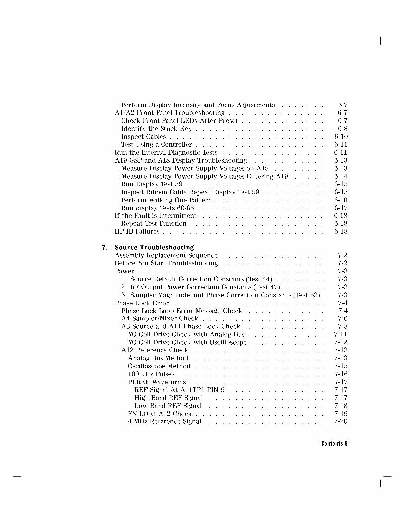
Perform Display Intensity and Focus Adjustments . . . . . . . 6-7A1/A2 Front Panel Troubleshooting . . . . . . . . . . . . . . . 6-7Check Front Panel LEDs After Preset . . . . . . . . . . . . . 6-7Identify the Stuck Key . . . . . . . . . . . . . . . . . . . . 6-8Inspect Cables . . . . . . . . . . . . . . . . . . . . . . . . 6-10Test Using a Controller . . . . . . . . . . . . . . . . . . . . 6-11
Run the Internal Diagnostic Tests . . . . . . . . . . . . . . . . 6-11A19 GSP and A18 Display Troubleshooting . . . . . . . . . . . 6-13
Measure Display Power Supply Voltages on A19 . . . . . . . . 6-13Measure Display Power Supply Voltages Entering A19 . . . . . 6-14Run Display Test 59 . . . . . . . . . . . . . . . . . . . . . 6-15Inspect Ribbon Cable Repeat Display Test 59 . . . . . . . . . . 6-15Perform Walking One Pattern . . . . . . . . . . . . . . . . . 6-16
Run display Tests 60-65 . . . . . . . . . . . . . . . . . . . 6-17
If the Fault is Intermittent . . . . . . . . . . . . . . . . . . . 6-18Repeat Test Function . . . . . . . . . . . . . . . . . . . . . 6-18
HP-IB Failures . . . . . . . . . . . . . . . . . . . . . . . . . 6-18
7. Source Troubleshooting
Assembly Replacement Sequence . . . . . . . . . . . . . . . . 7-2Before You Start Troubleshooting . . . . . . . . . . . . . . . . 7-2
Power . . . . . . . . . . . . . . . . . . . . . . . . . . . . . 7-3
1. Source Default Correction Constants (Test 44) . . . . . . . . 7-3
2. RF Output Power Correction Constants (Test 47) . . . . . . 7-3
3. Sampler Magnitude and Phase Correction Constants (Test 53) 7-3
Phase Lock Error . . . . . . . . . . . . . . . . . . . . . . . 7-4Phase Lock Loop Error Message Check . . . . . . . . . . . . 7-4
A4 Sampler/Mixer Check . . . . . . . . . . . . . . . . . . . 7-6
A3 Source and A11 Phase Lock Check . . . . . . . . . . . . 7-8YO Coil Drive Check with Analog Bus . . . . . . . . . . . . 7-11YO Coil Drive Check with Oscilloscope . . . . . . . . . . . 7-12
A12 Reference Check . . . . . . . . . . . . . . . . . . . . 7-13Analog Bus Method . . . . . . . . . . . . . . . . . . . . 7-13Oscilloscope Method . . . . . . . . . . . . . . . . . . . . 7-15
100 kHz Pulses . . . . . . . . . . . . . . . . . . . . . . 7-16
PLREF Waveforms . . . . . . . . . . . . . . . . . . . . . 7-17REF Signal At A11TP1 PIN 9 . . . . . . . . . . . . . . . 7-17
High Band REF Signal . . . . . . . . . . . . . . . . . . 7-17
Low Band REF Signal . . . . . . . . . . . . . . . . . . 7-18
FN LO at A12 Check . . . . . . . . . . . . . . . . . . . . 7-19
4 MHz Reference Signal . . . . . . . . . . . . . . . . . . 7-20
Contents-9

2ND LO Waveforms . . . . . . . . . . . . . . . . . . . . 7-2190 Degree Phase O�set of 2nd LO Signals in High Band . . 7-21In-Phase 2nd LO Signals in Low Band . . . . . . . . . . . 7-22
A12 Digital Control Signals Check . . . . . . . . . . . . . . 7-23L ENREF Line . . . . . . . . . . . . . . . . . . . . . . 7-23L HB and L LB Lines . . . . . . . . . . . . . . . . . . . 7-24
A13/A14 Fractional-N Check . . . . . . . . . . . . . . . . . 7-24Fractional-N Check with Analog Bus . . . . . . . . . . . . 7-24
A14 VCO Range Check with Oscilloscope . . . . . . . . . . 7-26A14 VCO Exercise . . . . . . . . . . . . . . . . . . . . . 7-28A14 Divide-by-N Circuit Check . . . . . . . . . . . . . . . 7-29A14-to-A13 Digital Control Signals Check. . . . . . . . . . . 7-30H MB Line . . . . . . . . . . . . . . . . . . . . . . . 7-32
A7 Pulse Generator Check . . . . . . . . . . . . . . . . . . 7-33
A7 Pulse Generator Check with Spectrum Analyzer . . . . . 7-33Rechecking the A13/A14 Fractional-N . . . . . . . . . . . . 7-35
A7 Pulse Generator Check with Oscilloscope . . . . . . . . . 7-35
A11 Phase Lock Check . . . . . . . . . . . . . . . . . . . . 7-37
Phase Lock Check with PLL DIAG . . . . . . . . . . . . . 7-37
Phase Lock Check by Signal Examination . . . . . . . . . . 7-37
Source Group Troubleshooting Appendix . . . . . . . . . . . . 7-39Troubleshooting Source Problems with the Analog Bus . . . . . 7-39
Phase Lock Diagnostic Tools . . . . . . . . . . . . . . . . . 7-39
Phase Lock Error Messages . . . . . . . . . . . . . . . . . 7-39
Phase Lock Diagnostic Routines . . . . . . . . . . . . . . . 7-40
Broadband Power Problems . . . . . . . . . . . . . . . . . 7-40
8. Receiver Troubleshooting
Assembly Replacement Sequence . . . . . . . . . . . . . . . . 8-2Receiver Failure Error Messages . . . . . . . . . . . . . . . . 8-2CAUTION: OVERLOAD ON REFL PORT, POWER REDUCED . . . . . . 8-2CAUTION: OVERLOAD ON TRANS PORT, POWER REDUCED . . . . . . 8-3
Check the R, A, and B Inputs . . . . . . . . . . . . . . . . . . 8-4Troubleshooting When All Inputs Look Bad . . . . . . . . . . . 8-7
Run Internal Tests 18 and 17 . . . . . . . . . . . . . . . . . 8-7
Check the 4 MHz REF Signal . . . . . . . . . . . . . . . . . . 8-8Check A10 by Substitution or Signal Examination . . . . . . . 8-8
Troubleshooting When One or More Inputs Look Good . . . . . . 8-11
Check the Frequency Response Correction . . . . . . . . . . 8-11
Check the 4 kHz Signal . . . . . . . . . . . . . . . . . . . . 8-11
Check 1st LO Signal at Sampler/Mixer . . . . . . . . . . . . . 8-12
Contents-10

Check 2nd LO Signal at Sampler/Mixer . . . . . . . . . . . . 8-13Check Input Trace . . . . . . . . . . . . . . . . . . . . . . 8-14
9. Accessories TroubleshootingAssembly Replacement Sequence . . . . . . . . . . . . . . . . 9-2Inspect the Accessories . . . . . . . . . . . . . . . . . . . . . 9-3Inspect the Test Port Connectors and Calibration Devices . . . . 9-3
Inspect the Error Terms . . . . . . . . . . . . . . . . . . . . 9-3
Cable Test . . . . . . . . . . . . . . . . . . . . . . . . . . 9-5Verify Shorts and Opens . . . . . . . . . . . . . . . . . . . 9-6
10. Service Key Menus and Error MessagesService Key Menus . . . . . . . . . . . . . . . . . . . . . . . 10-1
Error Messages . . . . . . . . . . . . . . . . . . . . . . . . 10-1
Service Key Menus - Internal Diagnostics . . . . . . . . . . . . 10-2Tests Menu . . . . . . . . . . . . . . . . . . . . . . . . . 10-3
Test Options Menu . . . . . . . . . . . . . . . . . . . . . . 10-5
Self Diagnose Softkey . . . . . . . . . . . . . . . . . . . . 10-7
Test Descriptions . . . . . . . . . . . . . . . . . . . . . . . 10-7
Internal Tests . . . . . . . . . . . . . . . . . . . . . . . 10-7External Tests . . . . . . . . . . . . . . . . . . . . . . . 10-12
System Veri�cation Tests . . . . . . . . . . . . . . . . . . 10-13
Adjustment Tests . . . . . . . . . . . . . . . . . . . . . 10-14
Display Tests . . . . . . . . . . . . . . . . . . . . . . . 10-16
Test Patterns . . . . . . . . . . . . . . . . . . . . . . . 10-17Service Key Menus - Service Features . . . . . . . . . . . . . . 10-19
Service Modes Menu . . . . . . . . . . . . . . . . . . . . . 10-20
Service Modes More Menu . . . . . . . . . . . . . . . . . . 10-23
Analog Bus . . . . . . . . . . . . . . . . . . . . . . . . . 10-25Description of the Analog Bus . . . . . . . . . . . . . . . 10-25The Main ADC . . . . . . . . . . . . . . . . . . . . . . . 10-25The Frequency Counter . . . . . . . . . . . . . . . . . . 10-25
Analog In Menu . . . . . . . . . . . . . . . . . . . . . . . 10-27Analog Bus Nodes . . . . . . . . . . . . . . . . . . . . . . 10-29
A3 Source . . . . . . . . . . . . . . . . . . . . . . . . . 10-29
A10 Digital IF . . . . . . . . . . . . . . . . . . . . . . . 10-36A11 Phase Lock . . . . . . . . . . . . . . . . . . . . . . 10-37
A12 Reference . . . . . . . . . . . . . . . . . . . . . . . 10-44
A14 Fractional-N (Digital) . . . . . . . . . . . . . . . . . 10-47
PEEK/POKE Menu . . . . . . . . . . . . . . . . . . . . . . 10-50
Firmware Revision Softkey . . . . . . . . . . . . . . . . . . . 10-51
Contents-11
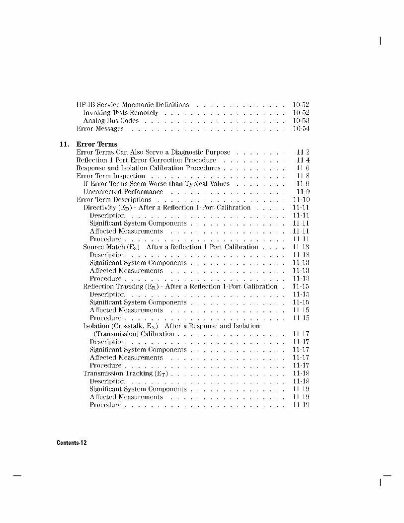
HP-IB Service Mnemonic De�nitions . . . . . . . . . . . . . . 10-52Invoking Tests Remotely . . . . . . . . . . . . . . . . . . . 10-52Analog Bus Codes . . . . . . . . . . . . . . . . . . . . . . 10-53
Error Messages . . . . . . . . . . . . . . . . . . . . . . . . 10-54
11. Error TermsError Terms Can Also Serve a Diagnostic Purpose . . . . . . . . 11-2Re ection 1-Port Error-Correction Procedure . . . . . . . . . . 11-4
Response and Isolation Calibration Procedures . . . . . . . . . . 11-6Error Term Inspection . . . . . . . . . . . . . . . . . . . . . 11-8If Error Terms Seem Worse than Typical Values . . . . . . . . 11-9Uncorrected Performance . . . . . . . . . . . . . . . . . . 11-9
Error Term Descriptions . . . . . . . . . . . . . . . . . . . . 11-10
Directivity (ED) - After a Re ection 1-Port Calibration . . . . . 11-11
Description . . . . . . . . . . . . . . . . . . . . . . . . 11-11Signi�cant System Components . . . . . . . . . . . . . . . 11-11
A�ected Measurements . . . . . . . . . . . . . . . . . . 11-11
Procedure . . . . . . . . . . . . . . . . . . . . . . . . . 11-11
Source Match (ES) - After a Re ection 1-Port Calibration . . . . 11-13
Description . . . . . . . . . . . . . . . . . . . . . . . . 11-13Signi�cant System Components . . . . . . . . . . . . . . . 11-13
A�ected Measurements . . . . . . . . . . . . . . . . . . 11-13
Procedure . . . . . . . . . . . . . . . . . . . . . . . . . 11-13
Re ection Tracking (ER) - After a Re ection 1-Port Calibration . 11-15
Description . . . . . . . . . . . . . . . . . . . . . . . . 11-15
Signi�cant System Components . . . . . . . . . . . . . . . 11-15A�ected Measurements . . . . . . . . . . . . . . . . . . 11-15
Procedure . . . . . . . . . . . . . . . . . . . . . . . . . 11-15
Isolation (Crosstalk, EX) - After a Response and Isolation(Transmission) Calibration . . . . . . . . . . . . . . . . . 11-17
Description . . . . . . . . . . . . . . . . . . . . . . . . 11-17Signi�cant System Components . . . . . . . . . . . . . . . 11-17A�ected Measurements . . . . . . . . . . . . . . . . . . 11-17Procedure . . . . . . . . . . . . . . . . . . . . . . . . . 11-17
Transmission Tracking (ET) . . . . . . . . . . . . . . . . . . 11-19
Description . . . . . . . . . . . . . . . . . . . . . . . . 11-19Signi�cant System Components . . . . . . . . . . . . . . . 11-19
A�ected Measurements . . . . . . . . . . . . . . . . . . 11-19
Procedure . . . . . . . . . . . . . . . . . . . . . . . . . 11-19
Contents-12

12. Theory of OperationHow the HP 8752C Works . . . . . . . . . . . . . . . . . . . 12-2The Built-In Synthesized Source . . . . . . . . . . . . . . . 12-3The Source Step Attenuator (Option 004) . . . . . . . . . . 12-3
The Built-In Transmission/Re ection Test Set . . . . . . . . . 12-4The Receiver Block . . . . . . . . . . . . . . . . . . . . . 12-4The Microprocessor . . . . . . . . . . . . . . . . . . . . 12-4
A Close Look at the Analyzer's Functional Groups . . . . . . . . 12-5
Power Supply Theory . . . . . . . . . . . . . . . . . . . . . 12-6A15 Preregulator . . . . . . . . . . . . . . . . . . . . . . 12-6Line Power Module . . . . . . . . . . . . . . . . . . . . 12-7Preregulated Voltages . . . . . . . . . . . . . . . . . . . 12-7Regulated +5V Digital Supply . . . . . . . . . . . . . . . 12-7
Shutdown Indications: the Green LED and Red LED . . . . . 12-7
A8 Post Regulator . . . . . . . . . . . . . . . . . . . . . . 12-8Voltage Indications: the Green LEDs . . . . . . . . . . . . 12-8
Shutdown Circuit . . . . . . . . . . . . . . . . . . . . . 12-8
Variable Fan Circuit and Air Flow Detector . . . . . . . . . 12-8
Display Power . . . . . . . . . . . . . . . . . . . . . . . 12-9
Probe Power . . . . . . . . . . . . . . . . . . . . . . . 12-9
Digital Control Theory . . . . . . . . . . . . . . . . . . . . . 12-9A1 Front Panel Keyboard . . . . . . . . . . . . . . . . . . 12-10
A2 Front Panel Processor . . . . . . . . . . . . . . . . . . . 12-11
A9 CPU/A10 Digital IF . . . . . . . . . . . . . . . . . . . . 12-11
Main CPU . . . . . . . . . . . . . . . . . . . . . . . . . 12-11
Main RAM . . . . . . . . . . . . . . . . . . . . . . . . . 12-11EEPROM . . . . . . . . . . . . . . . . . . . . . . . . . 12-12
Digital Signal Processor . . . . . . . . . . . . . . . . . . 12-12
A18 Display . . . . . . . . . . . . . . . . . . . . . . . . . 12-12A19 GSP . . . . . . . . . . . . . . . . . . . . . . . . . . 12-12A16 Rear Panel . . . . . . . . . . . . . . . . . . . . . . . 12-13
Source Theory Overview . . . . . . . . . . . . . . . . . . . . 12-14A14/A13 Fractional-N . . . . . . . . . . . . . . . . . . . . 12-14A12 Reference . . . . . . . . . . . . . . . . . . . . . . . . 12-14
A7 Pulse Generator . . . . . . . . . . . . . . . . . . . . . 12-14
A11 Phase Lock . . . . . . . . . . . . . . . . . . . . . . . 12-15
A3 Source . . . . . . . . . . . . . . . . . . . . . . . . . . 12-15Source Low Band Operation . . . . . . . . . . . . . . . . . . 12-16
Source High Band Operation . . . . . . . . . . . . . . . . . . 12-19
Signal Separation . . . . . . . . . . . . . . . . . . . . . . . 12-23
The A30 Dual Directional Coupler . . . . . . . . . . . . . . 12-23
Contents-13

Receiver Theory . . . . . . . . . . . . . . . . . . . . . . . . 12-23A4/A5/A6 Sampler/Mixer . . . . . . . . . . . . . . . . . . . 12-28The Sampler Circuit in High Band . . . . . . . . . . . . . . 12-28The Sampler Circuit in Low Band . . . . . . . . . . . . . . 12-28The 2nd LO Signal . . . . . . . . . . . . . . . . . . . . . 12-28The Mixer Circuit . . . . . . . . . . . . . . . . . . . . . 12-29
A10 Digital IF . . . . . . . . . . . . . . . . . . . . . . . . 12-29
13. Replaceable PartsAssembly Replacement Sequence . . . . . . . . . . . . . . . . 13-2Save Money with Rebuilt-Exchange Assemblies . . . . . . . . . 13-2Gather This Information Before Ordering . . . . . . . . . . . . 13-4Call (800) 227-8164 to Order Parts Fast (U.S. only) . . . . . . . 13-4
Replaceable Part Listings . . . . . . . . . . . . . . . . . . . . 13-5
Major Assemblies . . . . . . . . . . . . . . . . . . . . . . 13-6Front Panel Assemblies . . . . . . . . . . . . . . . . . . . . 13-8
Rear Panel Assemblies . . . . . . . . . . . . . . . . . . . . 13-10
Cables, Top View . . . . . . . . . . . . . . . . . . . . . . 13-12
Front Panel, Cables and Attaching Hardware . . . . . . . . . 13-14
Rear Panel, Cables and Attaching Hardware . . . . . . . . . . 13-16Source and Sampler Parts: Standard and Option 003 . . . . . . 13-18
Source and Sampler Parts: Option 004/006 . . . . . . . . . . 13-20
Source and Sampler Parts: Options 004 and 003/004 . . . . . . 13-22
Source and Sampler Parts: Option 006 . . . . . . . . . . . . 13-24
Display Bezel Assembly . . . . . . . . . . . . . . . . . . . 13-26
Chassis Parts . . . . . . . . . . . . . . . . . . . . . . . . 13-28Top View of Attaching Hardware and Post Regulator Fuses . . . 13-30
Bottom View of Attaching Hardware . . . . . . . . . . . . . 13-32
Right View of Attaching Hardware . . . . . . . . . . . . . . 13-34Left View of Attaching Hardware . . . . . . . . . . . . . . . 13-35
Rear Panel Attaching Hardware . . . . . . . . . . . . . . . 13-36Replaceable Labels . . . . . . . . . . . . . . . . . . . . . . 13-37Miscellaneous Parts and Accessories . . . . . . . . . . . . . . 13-38Abbreviations . . . . . . . . . . . . . . . . . . . . . . . . 13-40
Contents-14

14. Assembly Replacement and Post-Repair ProceduresAssembly Replacement Sequence . . . . . . . . . . . . . . . . 14-2Tools Required . . . . . . . . . . . . . . . . . . . . . . . . . 14-2Cover Removal Procedure . . . . . . . . . . . . . . . . . . . 14-3Initial Front Panel Procedure . . . . . . . . . . . . . . . . . . 14-4Initial Rear Panel Procedure . . . . . . . . . . . . . . . . . . 14-6A1, A2 Front Panel Keyboard, Interface . . . . . . . . . . . . . 14-8How to Remove the Front Panel Keyboard or Interface . . . . 14-8
Reverse Removal Procedure to Reinstall . . . . . . . . . . . . 14-9A3 Source . . . . . . . . . . . . . . . . . . . . . . . . . . . 14-10How to Remove the Source . . . . . . . . . . . . . . . . . . 14-10Reverse Removal Procedure to Reinstall . . . . . . . . . . . . 14-11
A15 Preregulator . . . . . . . . . . . . . . . . . . . . . . . 14-12
How to Remove the Preregulator . . . . . . . . . . . . . . . 14-12
Reverse Removal Procedure to Reinstall . . . . . . . . . . . . 14-13A16 Rear Panel Board Assembly . . . . . . . . . . . . . . . . 14-14
How to Remove the Rear Panel . . . . . . . . . . . . . . . . 14-14
Reverse Removal Procedure to Reinstall . . . . . . . . . . . . 14-15
A18 Display . . . . . . . . . . . . . . . . . . . . . . . . . . 14-16
How to Remove the Display . . . . . . . . . . . . . . . . . 14-16
How to Reinstall the Display . . . . . . . . . . . . . . . . . 14-17A30 Directional Coupler . . . . . . . . . . . . . . . . . . . . 14-18
How to Remove the Directional Coupler . . . . . . . . . . . . 14-18
Reverse Removal Procedure to Reinstall . . . . . . . . . . . . 14-19
B1 Fan . . . . . . . . . . . . . . . . . . . . . . . . . . . . 14-20
How to Remove the Fan . . . . . . . . . . . . . . . . . . . 14-20Reverse Removal Procedure to Reinstall . . . . . . . . . . . . 14-20
A9BT1 Battery . . . . . . . . . . . . . . . . . . . . . . . . 14-21
How to Remove the Battery . . . . . . . . . . . . . . . . . 14-21Replacing the Battery . . . . . . . . . . . . . . . . . . . . 14-21
Post-Repair Procedures . . . . . . . . . . . . . . . . . . . . . 14-22
15. Safety and LicensingNotice . . . . . . . . . . . . . . . . . . . . . . . . . . . . 15-1
Certi�cation . . . . . . . . . . . . . . . . . . . . . . . . . . 15-1
Assistance . . . . . . . . . . . . . . . . . . . . . . . . . . 15-1Shipment for Service . . . . . . . . . . . . . . . . . . . . . 15-3
Safety Symbols . . . . . . . . . . . . . . . . . . . . . . . . 15-4
Instrument Markings . . . . . . . . . . . . . . . . . . . . . . 15-5
General Safety Considerations . . . . . . . . . . . . . . . . . 15-6
Safety Earth Ground . . . . . . . . . . . . . . . . . . . . . 15-6
Contents-15

Before Applying Power . . . . . . . . . . . . . . . . . . . 15-6Servicing . . . . . . . . . . . . . . . . . . . . . . . . . . 15-6
Index
Contents-16

Figures
2-1. Measurement Uncertainty Window . . . . . . . . . . . . . . 2-52-2. Re ection Test Port Output Frequency Range and Accuracy Test
Setup . . . . . . . . . . . . . . . . . . . . . . . . . . 2-142-3. Re ection Test Port Output Power Range and Level Linearity Test
Setup . . . . . . . . . . . . . . . . . . . . . . . . . . 2-16
2-4. Re ection Test Port Output Power Range Test Setup (HP 8752C
Option 004) . . . . . . . . . . . . . . . . . . . . . . . 2-20
2-5. Re ection Test Port Output Power Level Linearity Test Setup . . 2-21
2-6. Transmission Test Port Input Noise Floor Level Test Setup 1 . . 2-252-7. Transmission Test Port Input Noise Floor Level Test Setup 2 . . 2-25
2-8. Transmission Test Port Input Noise Floor Level Test Setup 1 . . 2-27
2-9. Transmission Test Port Input Noise Floor Level Test Setup 2 . . 2-27
2-10. Transmission Test Port Input Noise Floor Level Test Setup 1 . . 2-30
2-11. Transmission Test Port Input Noise Floor Level Test Setup 2 . . 2-302-12. Test Port Crosstalk Test Setup . . . . . . . . . . . . . . . . . 2-33
2-13. Re ection Trace Noise Test Setup . . . . . . . . . . . . . . . 2-37
2-14. Transmission Trace Noise Test Setup . . . . . . . . . . . . . 2-38
2-15. Magnitude Dynamic Accuracy Test Setup . . . . . . . . . . . 2-42
2-16. Compression Test Setup . . . . . . . . . . . . . . . . . . . 2-483-1. Location of Major Assemblies . . . . . . . . . . . . . . . . . 3-6
3-2. NRM (Normal) and ALT (Alter) Positions of A9 CC Jumper . . . 3-73-3. Source Adjustment Setup . . . . . . . . . . . . . . . . . . . 3-113-4. Maximum Intensity Adjustment Set-up . . . . . . . . . . . . 3-173-5. IF Ampli�er Correction Constant Setup . . . . . . . . . . . . 3-193-6. Cavity Oscillator Frequency Correction Constant Setup . . . . . 3-243-7. Typical Target Spur Using Filter . . . . . . . . . . . . . . . 3-27
3-8. Cavity Oscillator Frequency Correction Alternative Setup . . . 3-28
3-9. Typical Display of Four Spurs without Filter . . . . . . . . . . 3-29
3-10. Typical Display of Five Spurs without Filter . . . . . . . . . . 3-30
3-11. Variation of Display of Four Spurs without Filter . . . . . . . . 3-313-12. Location of Keyword Label . . . . . . . . . . . . . . . . . . 3-34
3-13. EEPROM Backup Procedure Setup . . . . . . . . . . . . . . 3-38
Contents-17

3-14. Vertical Position and Focus Adjustment Controls . . . . . . . . 3-443-15. FN VCO TUNE Adjustment Location . . . . . . . . . . . . . 3-473-16. Fractional-N Frequency Range Adjustment Display . . . . . . . 3-483-17. Re ection Test Port Output Frequency Accuracy Adjustment
Setup . . . . . . . . . . . . . . . . . . . . . . . . . . 3-493-18. VCXO ADJ Adjustment Location . . . . . . . . . . . . . . . 3-503-19. High/Low Band Transition Adjustment Trace . . . . . . . . . 3-523-20. High/Low Band Adjustments Locations . . . . . . . . . . . . 3-52
3-21. Fractional-N Spur Avoidance and FM Sideband Adjustment Setup 3-553-22. Location of API and 100 kHz Adjustments . . . . . . . . . . . 3-563-23. A11 Test Point and A3 CAV ADJ Locations . . . . . . . . . . 3-583-24. Display of Acceptable Versus Excessive Spikes . . . . . . . . . 3-594-1. LED Power-up Sequence . . . . . . . . . . . . . . . . . . . 4-3
4-2. Troubleshooting Organization . . . . . . . . . . . . . . . . . 4-10
4-3. A15 Preregulator LEDs . . . . . . . . . . . . . . . . . . . . 4-114-4. Front Panel Power-up Sequence . . . . . . . . . . . . . . . 4-12
4-5. Equipment Setup for Source Power Check . . . . . . . . . . . 4-14
4-6. Typical Measurement Trace . . . . . . . . . . . . . . . . . 4-15
4-7. HP 8752C Overall Block Diagram (1 of 4) . . . . . . . . . . . 4-17
5-1. Power Supply Group Simpli�ed Block Diagram . . . . . . . . . 5-3
5-2. Location of A15 Diagnostic LEDs . . . . . . . . . . . . . . . 5-45-3. A8 Post Regulator Test Point Locations . . . . . . . . . . . . 5-5
5-4. Removing the Line Fuse . . . . . . . . . . . . . . . . . . . 5-7
5-5. Power Supply Cable Locations . . . . . . . . . . . . . . . . 5-9
5-6. A15W1 Plug Detail . . . . . . . . . . . . . . . . . . . . . . 5-11
5-7. Front Panel Probe Power Connector Voltages . . . . . . . . . 5-205-8. Power Supply Block Diagram . . . . . . . . . . . . . . . . . 5-25
6-1. Digital Control Group Block Diagram . . . . . . . . . . . . . 6-3
6-2. Jumper Positions on the A9 CPU . . . . . . . . . . . . . . . 6-46-3. Location of Four LEDs on A9 CPU . . . . . . . . . . . . . . 6-56-4. Preset Sequence . . . . . . . . . . . . . . . . . . . . . . . 6-86-5. Pin Locations on A19J5 . . . . . . . . . . . . . . . . . . . 6-136-6. Pin Locations on Connector of W14 . . . . . . . . . . . . . . 6-146-7. A9 CPU Walking One Pattern . . . . . . . . . . . . . . . . . 6-16
6-8. Pin Locations on Connector of W20 . . . . . . . . . . . . . . 6-17
7-1. Phase Lock Error Troubleshooting Equipment Setup . . . . . . 7-4
7-2. Jumper Positions on the A9 CPU . . . . . . . . . . . . . . . 7-57-3. Sampler/Mixer to Phase Lock Cable Connection Diagram . . . . 7-7
7-4. Waveform Integrity in SRC Tune Mode . . . . . . . . . . . . 7-9
7-5. Phase Locked Output Compared to Open Loop Output in SRCTune Mode . . . . . . . . . . . . . . . . . . . . . . . . 7-9
Contents-18

7-6. 1V/GHz at Analog Bus Node 16 with Source PLL O�. . . . . . 7-117-7. YO� and YO+ Coil Drive Voltage Di�erences with SOURCE PLL
OFF . . . . . . . . . . . . . . . . . . . . . . . . . . . 7-127-8. Sharp 100 kHz Pulses at A13TP5 (any frequency) . . . . . . . 7-167-9. High Band REF Signal (�16 MHz CW) . . . . . . . . . . . . . 7-177-10. REF Signal at A11TP9 (5 MHz CW) . . . . . . . . . . . . . . 7-187-11. Typical FN LO Waveform at A12J1 . . . . . . . . . . . . . . 7-197-12. 4 MHz Reference Signal at A12TP9 (Preset) . . . . . . . . . . 7-20
7-13. 90 Degree Phase O�set of High Band 2nd LO Signals (�16 MHzCW) . . . . . . . . . . . . . . . . . . . . . . . . . . . 7-21
7-14. In-Phase Low Band 2nd LO Signals (14 MHz CW) . . . . . . . . 7-227-15. L ENREF Line at A12P2-16 (Preset) . . . . . . . . . . . . . . 7-237-16. Complementary L HB and L LB Signals (Preset) . . . . . . . . 7-24
7-17. 10 MHz HI OUT Waveform from A14J1 . . . . . . . . . . . . 7-26
7-18. 25 MHz HI OUT Waveform from A14J1 . . . . . . . . . . . . 7-277-19. 60 MHz HI OUT Waveform from A14J1 . . . . . . . . . . . . 7-27
7-20. LO OUT Waveform at A14J2 . . . . . . . . . . . . . . . . . 7-28
7-21. A14 Generated Digital Control Signals . . . . . . . . . . . . . 7-31
7-22. H MB Signal at A14P1-5 (Preset and 16 MHz to 31 MHz Sweep) . 7-32
7-23. Pulse Generator Output . . . . . . . . . . . . . . . . . . . 7-33
7-24. High Quality Comb Tooth at 3 GHz . . . . . . . . . . . . . . 7-347-25. Stable HI OUT Signal in FRACN TUNE Mode . . . . . . . . . . 7-35
7-26. Typical 1st IF Waveform in FRACN TUNE/SRC TUNE Mode . . 7-36
7-27. FM Coil { Plot with 3 Point Sweep . . . . . . . . . . . . . . 7-38
8-1. Sample R Input Trace . . . . . . . . . . . . . . . . . . . . 8-4
8-2. Sample A Input Trace . . . . . . . . . . . . . . . . . . . . 8-58-3. Sample B Input Trace . . . . . . . . . . . . . . . . . . . . 8-6
8-4. 4 MHz REF Waveform . . . . . . . . . . . . . . . . . . . . 8-8
8-5. Digital Data Lines Observed Using L INTCOP as Trigger . . . . 8-108-6. Digital Control Lines Observed Using L INTCOP as Trigger . . . 8-10
8-7. 2nd IF (4 kHz) Waveform . . . . . . . . . . . . . . . . . . . 8-129-1. Typical Return Loss Traces of Good and Poor Cables . . . . . . 9-59-2. Typical Smith Chart Traces of Good Short (a) and Open (b) . . . 9-710-1. Internal Diagnostics Menus . . . . . . . . . . . . . . . . . . 10-2
10-2. Jumper Positions on the A9 CPU . . . . . . . . . . . . . . . 10-9
10-3. Service Feature Menus . . . . . . . . . . . . . . . . . . . . 10-19
10-4. Analog Bus Node 1 . . . . . . . . . . . . . . . . . . . . . 10-3010-5. Analog Bus Node 2 . . . . . . . . . . . . . . . . . . . . . 10-31
10-6. Analog Bus Node 3 . . . . . . . . . . . . . . . . . . . . . 10-32
10-7. Analog Bus Node 4 . . . . . . . . . . . . . . . . . . . . . 10-33
10-8. Analog Bus Node 6 . . . . . . . . . . . . . . . . . . . . . 10-34
Contents-19

10-9. Analog Bus Node 7 . . . . . . . . . . . . . . . . . . . . . 10-3510-10. Analog Bus Node 14 . . . . . . . . . . . . . . . . . . . . . 10-3810-11. Analog Bus Node 15 . . . . . . . . . . . . . . . . . . . . . 10-3910-12. Analog Bus Node 16 . . . . . . . . . . . . . . . . . . . . . 10-4010-13. Counter Readout Location . . . . . . . . . . . . . . . . . . 10-4110-14. Analog Bus Node 18 . . . . . . . . . . . . . . . . . . . . . 10-4210-15. Analog Bus Node 20 . . . . . . . . . . . . . . . . . . . . . 10-4310-16. Analog Bus Node 23 . . . . . . . . . . . . . . . . . . . . . 10-45
10-17. Analog Bus Node 29 . . . . . . . . . . . . . . . . . . . . . 10-4810-18. Analog Bus Node 30 . . . . . . . . . . . . . . . . . . . . . 10-4910-19. Location of Firmware Revision Information on Display . . . . . 10-5111-1. Standard Connections for One-Port Error-Correction . . . . . . 11-411-2. Standard Connections for Response Calibration . . . . . . . . 11-6
11-3. Standard Connections for Isolation Calibration . . . . . . . . . 11-7
11-4. Typical ED (Re ection Test Port) . . . . . . . . . . . . . . . 11-1211-5. Typical ES (Re ection Test Port) . . . . . . . . . . . . . . . 11-14
11-6. Typical ER (Re ection Test Port) . . . . . . . . . . . . . . . 11-16
11-7. Typical EX with 10 Hz Bandwidth . . . . . . . . . . . . . . 11-18
11-8. Typical EX with 3 kHz Bandwidth . . . . . . . . . . . . . . 11-18
11-9. Typical ET . . . . . . . . . . . . . . . . . . . . . . . . . 11-20
12-1. Simpli�ed Block Diagram of the Network Analyzer System . . . 12-212-2. Power Supply Functional Group, Simpli�ed Block Diagram . . . 12-6
12-3. Digital Control Group, Block Diagram . . . . . . . . . . . . . 12-10
12-4. Low Band Operation of the Source . . . . . . . . . . . . . . 12-17
12-5. High Band Operation of the Source . . . . . . . . . . . . . . 12-21
12-6. Receiver Functional Group (standard and Option 003) . . . . . 12-2412-7. Receiver Functional Group (Option 003 and 004) . . . . . . . . 12-25
12-8. Receiver Functional Group (Option 006) . . . . . . . . . . . . 12-26
12-9. Receiver Functional Group (Option 004 and 006) . . . . . . . . 12-2713-1. Module Exchange Procedure . . . . . . . . . . . . . . . . . 13-314-1. Cover Removal Procedure . . . . . . . . . . . . . . . . . . 14-314-2. Initial Front Panel Procedure . . . . . . . . . . . . . . . . . 14-414-3. Location of Screws on Bottom Edge of Frame . . . . . . . . . 14-514-4. Location of EXT REF cable and GSP Assembly . . . . . . . . 14-6
14-5. Location of Rear Panel Fasteners . . . . . . . . . . . . . . . 14-7
14-6. Location of A1 and A2 components . . . . . . . . . . . . . . 14-8
14-7. Location of Source Parts . . . . . . . . . . . . . . . . . . . 14-1014-8. Location of Preregulator Fasteners and Wires . . . . . . . . . 14-12
14-9. Location of Rear Panel Fasteners . . . . . . . . . . . . . . . 14-14
14-10. Location of Display Fasteners and Parts . . . . . . . . . . . . 14-16
14-11. Location of Coupler Screws on Bottom Front Frame . . . . . . 14-18
Contents-20

14-12. Location of Directional Coupler Hardware . . . . . . . . . . . 14-1914-13. Location of Fan Wire Bundle and Screws . . . . . . . . . . . 14-20
Contents-21

Tables
1-1. Service Test Equipment . . . . . . . . . . . . . . . . . . . 1-21-2. Required Tools . . . . . . . . . . . . . . . . . . . . . . . . 1-41-3. Connector Care Quick Reference . . . . . . . . . . . . . . . 1-65-1. A8 Post Regulator Test Point Voltages . . . . . . . . . . . . . 5-6
5-2. Output Voltages . . . . . . . . . . . . . . . . . . . . . . . 5-105-3. Recommended Order for Removal/Disconnection . . . . . . . . 5-12
5-4. Recommended Order for Removal/Disconnection . . . . . . . . 5-18
6-1. LED Code and Pattern Versus Test Failed . . . . . . . . . . . 6-6
6-2. Front Panel Key Codes . . . . . . . . . . . . . . . . . . . . 6-9
6-3. Internal Diagnostic Test with Commentary . . . . . . . . . . . 6-12
7-1. Output Frequency in SRC Tune Mode . . . . . . . . . . . . . 7-87-2. Analog Bus Check of Reference Frequencies . . . . . . . . . . 7-13
7-3. A12 Reference Frequencies . . . . . . . . . . . . . . . . . . 7-15
7-4. A12-Related Digital Control Signals . . . . . . . . . . . . . . 7-23
7-5. VCO Range Check Frequencies . . . . . . . . . . . . . . . . 7-25
7-6. A14-to-A13 Digital Control Signal Locations . . . . . . . . . . 7-307-7. 1st IF Waveform Settings . . . . . . . . . . . . . . . . . . . 7-36
7-8. A11 Input Signals . . . . . . . . . . . . . . . . . . . . . . 7-38
8-1. Signals Required for A10 Assembly Operation . . . . . . . . . 8-9
8-2. 2nd IF (4 kHz) Signal Locations . . . . . . . . . . . . . . . . 8-128-3. 2nd LO Locations . . . . . . . . . . . . . . . . . . . . . . 8-139-1. Components Related to Speci�c Error Terms . . . . . . . . . . 9-410-1. Test Status Terms . . . . . . . . . . . . . . . . . . . . . . 10-410-2. Descriptions of Jumper Positions . . . . . . . . . . . . . . . 10-811-1. Calibration Coe�cient Terms and Tests . . . . . . . . . . . . 11-7
11-2. Uncorrected System Performance . . . . . . . . . . . . . . . 11-9
12-1. Low Band Subsweep Frequencies . . . . . . . . . . . . . . . 12-1812-2. High Band Subsweep Frequencies . . . . . . . . . . . . . . . 12-22
12-3. Mixer Frequencies . . . . . . . . . . . . . . . . . . . . . . 12-29
14-1. Post-Repair Procedures . . . . . . . . . . . . . . . . . . . . 14-22
Contents-22

1
Service Equipment and Analyzer Options
Table of Service Test Equipment
The following tables list the tools and test equipment required to perform theanalyzer's system veri�cation, troubleshooting, adjustment, and performancetests.
Service Equipment and Analyzer Options 1-1

Table 1-1. Service Test Equipment
Required
Equipment
Critical
Speci�cations
Recommended
Model
Use*
Spectrum Analyzer Freq. Accuracy �7 Hz HP 8563E A, T
Frequency Counter HP 5343A P
Measuring Receiver HP 8902A P
Oscilloscope Bandwidth: 100 MHz
Accuracy: 10%
any T
Digital Voltmeter Resolution: 10 mV any T
Tool Kit No substitute HP part number
08753-60023
T
Power Meter (HP-IB) No substitute HP 436A Opt. 022,
HP 437A or 438A
A, P, T
Power Sensor Frequency: 300 kHz-3 GHz, 50 HP 8482A A, P, T
Power Sensor (for Option 006) Frequency: 3 GHz-6 GHz HP 8481A Opt 006 A, P, T
Power Sensor Frequency: 300 kHz-3 GHz, 75 HP 8483A Opt. H03 P
Photometer Tektronix J16 A
Photometer Probe Tektronix J6503 A
Light Occluder Tektronix
016-0305-00
A
CRT Demagnetizer or Bulk Tape
Eraser
A
Printer HP ThinkJet,
DeskJet, LaserJet
P
Disk Drive 3.5-inch HP 9122
Floppy Disk 3.5-inch HP 92192A A
Calibration Kit Type-N, 50 No substitute HP 85032B P
Calibration Kit Type-N, 75 No substitute HP 85036B P
Veri�cation Kit 7 mm No substitute HP 85029B P
Low Pass Filter >50 dB @ 2.96 Hz and passband that
includes 800 MHz
HP P/N 9135-0198 A
Step Attenuator 110 dB HP 8496A P
Attenuators (�xed): Return loss: �32 dB APC-7 20 dB (2) HP 8491A Opt. 020 P, T
Power Splitter 2-Way, 50 HP 11667A P, T
Minimum Loss Pad Type-N, 50 to 75 HP 11852B P, T
1-2 Service Equipment and Analyzer Options

Table 1-2. Service Test Equipment (2 of 2)
Required
Equipment
Critical
Speci�cations
Recommended
Model
Use*
Adapter BNC to Alligator Clip HP P/N 8120-1292 A
Adapter APC-3.5 (m) to type-N (f) HP P/N 1250-1750 A, P
Adapter APC-3.5 (f) to type-N (f) HP P/N 1250-1745 A, P
Adapter APC-3.5 (f) to type-N (m) HP P/N 1250-1744 A
Adapter BNC (m) to type-N (f) HP P/N 1250-0077 P
Adapter type-N (m) to type-N (m) HP P/N 1250-1528 P
RF Cable 24-inch, type-N, 75 HP P/N 8120-2408 A, P
RF Cable 24-inch, type-N, 50 HP P/N 8120-4781 A, P
RF Cable Set type-N, 50 HP 11851B P
HP-IB Cable HP 10833A/B/C/D A
Coax Cable BNC HP P/N 8120-1840 A
Coax Cable BNC (m) to BNC (m), 50 HP 10503A A
Antistatic Wrist Strap HP P/N 9300-1367 A, T, P
Antistatic Wrist Strap Cord HP P/N 9300-0980 A, T, P
Static-control Table Mat and
Earth Ground Wire
HP P/N 9300-0797 A, T, P
* P - Performance Tests
A - Adjustment
T - Troubleshooting
Service Equipment and Analyzer Options 1-3

Table 1-2. Required Tools
T-8, T-10 and T-15 TORX screwdrivers
Flat-blade screwdrivers|small, medium, and large
5/16-inch open-end wrench (for SMA nuts)
3/16, 5/16, and 9/16-inch hex nut drivers
5/16-inch open-end torque wrench (set to 10 in-lb)
2.5-mm hex-key driver
Non-conductive and non-ferrous adjustment tool
Needle-nose pliers
Tweezers
Antistatic work mat with wrist-strap
1-4 Service Equipment and Analyzer Options
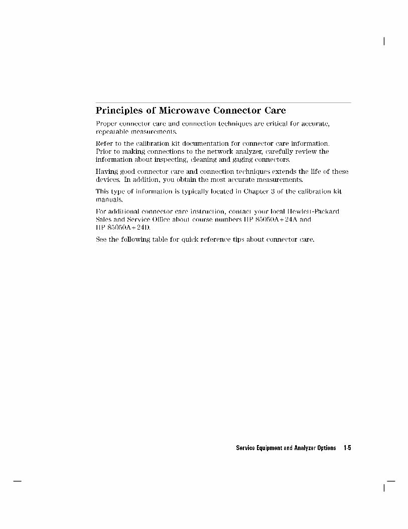
Principles of Microwave Connector Care
Proper connector care and connection techniques are critical for accurate,repeatable measurements.
Refer to the calibration kit documentation for connector care information.Prior to making connections to the network analyzer, carefully review theinformation about inspecting, cleaning and gaging connectors.
Having good connector care and connection techniques extends the life of thesedevices. In addition, you obtain the most accurate measurements.
This type of information is typically located in Chapter 3 of the calibration kitmanuals.
For additional connector care instruction, contact your local Hewlett-Packard
Sales and Service O�ce about course numbers HP 85050A+24A andHP 85050A+24D.
See the following table for quick reference tips about connector care.
Service Equipment and Analyzer Options 1-5

Table 1-3. Connector Care Quick Reference
Handling and Storage
Do Do Not
Keep connectors clean Touch mating-plane surfaces
Extend sleeve or connector nut Set connectors contact|end down
Use plastic end-caps during storage
Visual Inspection
Do Do Not
Inspect all connectors carefully Use a damaged connector|ever
Look for metal particles, scratches, and dents
Connector Cleaning
Do Do Not
Try compressed air �rst Use any abrasives
Use isopropyl alcohol Get liquid into plastic support beads
Clean connector threads
Gaging Connectors
Do Do Not
Clean and zero the gage before use Use an out-of-spec connector
Use the correct gage type
Use correct end of calibration block
Gage all connectors before �rst use
Making Connections
Do Do Not
Align connectors carefully Apply bending force to connection
Make preliminary connection lightly Over tighten preliminary connection
Turn only the connector nut Twist or screw any connection
Use a torque wrench for �nal connect Tighten past torque wrench \break" point
1-6 Service Equipment and Analyzer Options

Analyzer Options Available
Option 003, 3 GHz Operation
This option extends the maximum source and receiver frequency of the analyzerto 3 GHz.
Option 004, Step Attenuator
This option provides a source output power range from �85 to +10 dBm.
Option 006, 6 GHz Operation
This option extends the maximum source and receiver frequency of the analyzerto 6 GHz.
Option 010, Time Domain
This option displays the time domain response of a network by computingthe inverse Fourier transform of the frequency domain response. It showsthe response of a test device as a function of time or distance. Displaying the
re ection coe�cient of a network versus time determines the magnitude andlocation of each discontinuity. Displaying the transmission coe�cient of a
network versus time determines the characteristics of individual transmission
paths. Time domain operation retains all accuracy inherent with the correctionthat is active in such devices as SAW �lters, SAW delay lines, RF cables, and RF
antennas.
Option 075, 75 Impedance
This option o�ers 75 impedance bridges with type-N test port connectors.
Option 1CM, Rack Mount Flange Kit Without Handles
This option is a rack mount kit containing a pair of anges and the necessaryhardware to mount the instrument, with handles detached, in an equipmentrack with 482.6 mm (19 inches) horizontal spacing.
Service Equipment and Analyzer Options 1-7

Option 1CP, Rack Mount Flange Kit With Handles
This option is a rack mount kit containing a pair of anges and the necessaryhardware to mount the instrument with handles attached in an equipment rackwith 482.6 mm (19 inches) spacing.
Option AFN, add 50 Test Port Cable
This option provides a second type-N male to type-N male test port cable and atype-N female to type-N female adapter. Instructions are included for storing a
new internal calibration to account for the e�ects of this cable.
Option AFP, add 75 Test Port Cable
This option provides a 75 type-N male to type-N female test port cable.
Instructions are included for storing a new internal calibration to account forthe e�ects of this cable.
Option B02, External Disk Drive
This option provides an external disk drive and an HP-IB cable.
1-8 Service Equipment and Analyzer Options

Service and Support Options
Hewlett-Packards o�ers many repair and calibration options for your analyzer.Contact the nearest Hewlett-Packard sales or service o�ce for information onoptions available for your analyzer. See the table titled \Hewlett-Packard Salesand Service O�ces" in Chapter 15.
Service Equipment and Analyzer Options 1-9


2System Veri�cation and PerformanceTests
How to Test the Performance of Your Analyzer
To obtain the same quality of performance testing that Hewlett-Packard hasadministered at the factory, you must perform:
the system veri�cation procedure
AND
all of the performance test procedures.
This quality of performance testing guarantees that the analyzer is performingwithin all of the published speci�cations. A Hewlett-Packard Customer Engineer
will issue a Certi�cate of Calibration for your analyzer if two conditions aremet:
Your analyzer passes all the performed tests.
The equipment and standards that were used to perform the tests aretraceable to a national standards institute.
Note If you have a particular type of measurement application thatdoes not use all of the analyzer's measurement capabilities,you may ask your local Hewlett-Packard Customer ServiceCenter for a subset of speci�cations that you want veri�ed.However, this does create the potential for making incorrectmeasurements when using a di�erent application.
System Veri�cation and Performance Tests 2-1
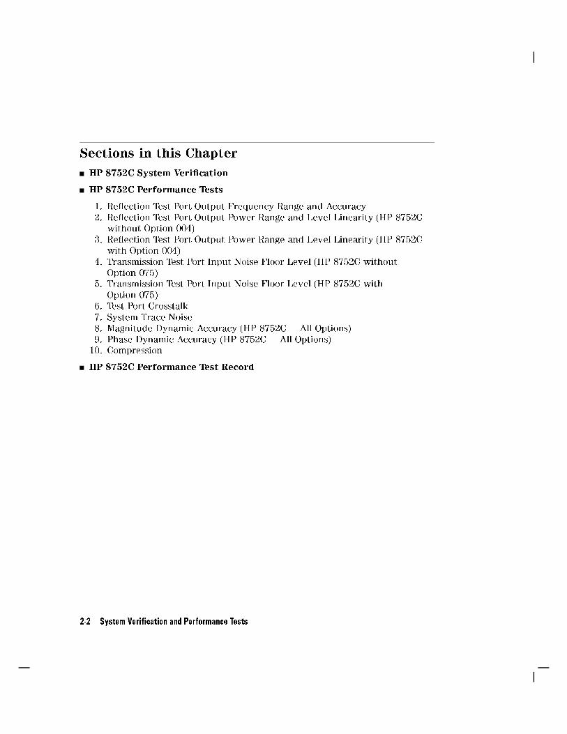
Sections in this Chapter
HP 8752C System Veri�cation
HP 8752C Performance Tests
1. Re ection Test Port Output Frequency Range and Accuracy2. Re ection Test Port Output Power Range and Level Linearity (HP 8752C
without Option 004)3. Re ection Test Port Output Power Range and Level Linearity (HP 8752C
with Option 004)4. Transmission Test Port Input Noise Floor Level (HP 8752C without
Option 075)5. Transmission Test Port Input Noise Floor Level (HP 8752C with
Option 075)6. Test Port Crosstalk
7. System Trace Noise
8. Magnitude Dynamic Accuracy (HP 8752C � All Options)
9. Phase Dynamic Accuracy (HP 8752C � All Options)10. Compression
HP 8752C Performance Test Record
2-2 System Veri�cation and Performance Tests
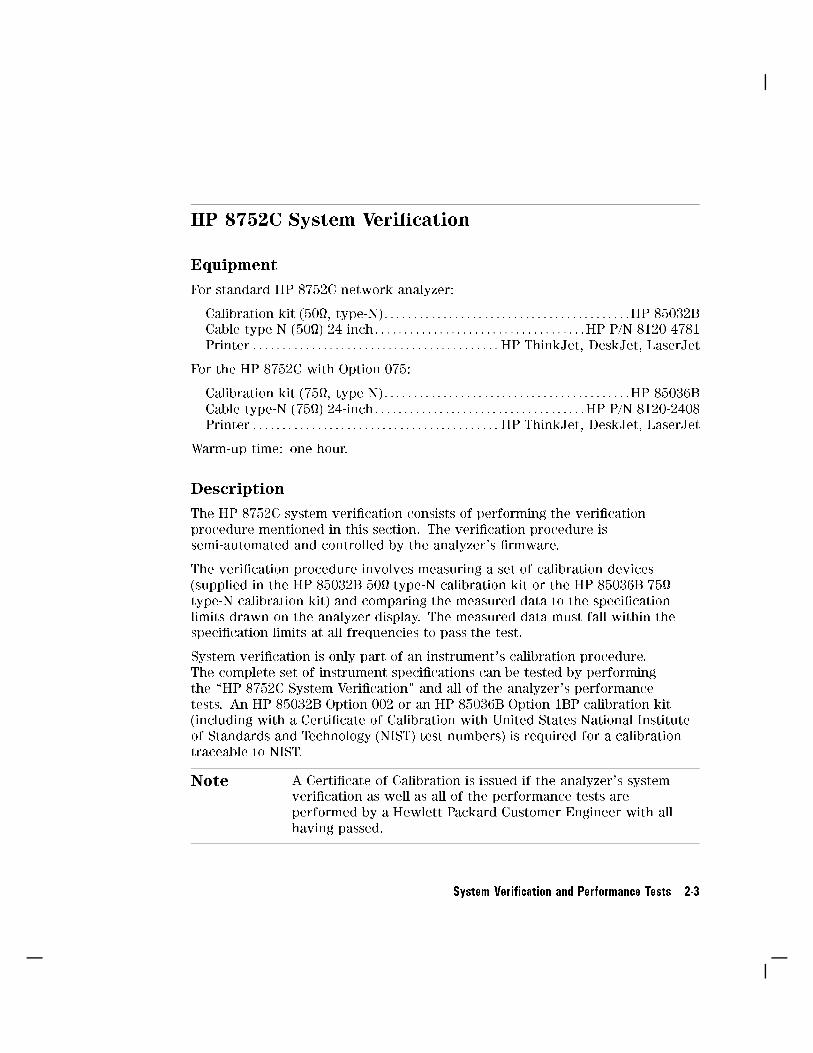
HP 8752C System Veri�cation
Equipment
For standard HP 8752C network analyzer:
Calibration kit (50, type-N) : : : : : : : : : : : : : : : : : : : : : : : : : : : : : : : : : : : : : : : : : :HP 85032BCable type-N (50) 24-inch : : : : : : : : : : : : : : : : : : : : : : : : : : : : : : : : : : : :HP P/N 8120-4781Printer : : : : : : : : : : : : : : : : : : : : : : : : : : : : : : : : : : : : : : : : : : HP ThinkJet, DeskJet, LaserJet
For the HP 8752C with Option 075:
Calibration kit (75, type-N) : : : : : : : : : : : : : : : : : : : : : : : : : : : : : : : : : : : : : : : : : :HP 85036BCable type-N (75) 24-inch : : : : : : : : : : : : : : : : : : : : : : : : : : : : : : : : : : : :HP P/N 8120-2408Printer : : : : : : : : : : : : : : : : : : : : : : : : : : : : : : : : : : : : : : : : : : HP ThinkJet, DeskJet, LaserJet
Warm-up time: one hour.
Description
The HP 8752C system veri�cation consists of performing the veri�cationprocedure mentioned in this section. The veri�cation procedure issemi-automated and controlled by the analyzer's �rmware.
The veri�cation procedure involves measuring a set of calibration devices(supplied in the HP 85032B 50 type-N calibration kit or the HP 85036B 75type-N calibration kit) and comparing the measured data to the speci�cationlimits drawn on the analyzer display. The measured data must fall within thespeci�cation limits at all frequencies to pass the test.
System veri�cation is only part of an instrument's calibration procedure.The complete set of instrument speci�cations can be tested by performing
the \HP 8752C System Veri�cation" and all of the analyzer's performancetests. An HP 85032B Option 002 or an HP 85036B Option 1BP calibration kit(including with a Certi�cate of Calibration with United States National Instituteof Standards and Technology (NIST) test numbers) is required for a calibration
traceable to NIST.
Note A Certi�cate of Calibration is issued if the analyzer's systemveri�cation as well as all of the performance tests areperformed by a Hewlett-Packard Customer Engineer with all
having passed.
System Veri�cation and Performance Tests 2-3

System Veri�cation Cycle and Kit Recerti�cation
The recommended system veri�cation cycle is every six months. Hewlett-Packard also suggests the calibration kit be recerti�ed annually. For moreinformation about the kit recerti�cation, refer to the HP 85032B 50 Type-NCalibration Kit Operation and Service Manual or HP 85036B 75 Type-NCalibration Kit Operation and Service Manual.
Measurement Uncertainty
Associated with any analyzer are measurement errors that add uncertainty tothe measured results. This uncertainty limits how accurately a device under test(DUT) can be measured.
The measurement uncertainty is de�ned to be the sum of the residualsystematic (repeatable) and random (non-repeatable) errors in the measurementsystem. The systematic errors are e�ective directivity, e�ective source match,
load match, re ection and transmission tracking, and isolation (crosstalk).
Random errors include errors due to noise, drift, connector repeatability, and
test cable stability.
The typical measurement uncertainties for type-N connectors using a1-port error correction utilize an RSS (Root Sum of Squares) model for thecontributions of random errors such as noise, pin depth, pin diameter variation,
load return loss, and connector repeatability.
Measurement Uncertainty Window
The PASS/FAIL result of the limit line test generally indicates the status of the
veri�cation test. The validity of the limit lines, drawn on the analyzer displayduring the veri�cation tests, are determined by the measurement uncertainty.
The measurement uncertainty must be taken into account when analyzingthe test results. If the analyzer detects the test data outside of the limits, aFAIL will be displayed on the analyzer. This FAIL status may not represent
a true failure if at the worst point, the test data is within the measurementuncertainty window (not displayed on the analyzer). Refer to Figure 2-1 forinterpretations of test data.
2-4 System Veri�cation and Performance Tests

Figure 2-1. Measurement Uncertainty Window
System Veri�cation and Performance Tests 2-5

HP 8752C Type-N Test Port Characteristics (50 System)
Directivity
Frequency Range Speci�cation Measurement Uncertainty
300 kHz to 1.3 GHz 40 dB1 �3.30 dB
1.3 GHz to 3.0 GHz 35 dB �2.51 dB
3.0 GHz to 6.0 GHz 30 dB �3.30 dB
1 30 dB, 300 kHz to 10 MHz
Source Match (Re ection)
Frequency Range Speci�cation Measurement Uncertainty
300 kHz to 1.3 GHz 30 dB �2.51 dB
1.3 GHz to 3.0 GHz 25 dB �2.88 dB
3.0 GHz to 6.0 GHz 20 dB �2.88 dB
Source Match (Transmission)*
Frequency Range Speci�cation Measurement Uncertainty
300 kHz to 1.3 GHz 23 dB �2.51 dB
1.3 GHz to 3.0 GHz 20 dB �2.88 dB
3.0 GHz to 6.0 GHz 16 dB �2.88 dB
*Option 004 may degrade transmission source match as much as 2 dB, resulting in up to 0.05 dB additional
uncertainty in transmission tracking.
Re ection Tracking
Frequency Range Speci�cation Measurement Uncertainty
300 kHz to 1.3 GHz �0.2 dB �0.009 dB
1.3 GHz to 3.0 GHz �0.3 dB �0.019 dB
3.0 GHz to 6.0 GHz �0.4 dB �0.070 dB
2-6 System Veri�cation and Performance Tests

Load Match
Frequency Range Speci�cation Measurement Uncertainty
300 kHz to 1.3 GHz 23 dB1 �0.40 dB
1.3 GHz to 3.0 GHz 20 dB �0.40 dB
3.0 GHz to 6.0 GHz 18 dB �0.92 dB
1 14 dB, 300 kHz to 10 MHz for analyzers with option 006
Transmission Tracking
Frequency Range Speci�cation Measurement Uncertainty
300 kHz to 1.3 GHz �0.2 dB �0.043 dB
1.3 GHz to 3.0 GHz �0.3 dB �0.086 dB
3.0 GHz to 6.0 GHz �0.5 dB �0.172 dB
HP 8752C Type-N Test Port Characteristics (75 System)
Directivity
Frequency Range Speci�cation Measurement Uncertainty
300 kHz to 10 MHz 30 dB �4.41 dB
10 MHz to 1.3 GHz 40 dB �4.41 dB
1.3 GHz to 3.0 GHz 35 dB �4.41 dB
Source Match (Re ection)
Frequency Range Speci�cation Measurement Uncertainty
300 kHz to 1.3 GHz 30 dB �2.88 dB
1.3 GHz to 3.0 GHz 25 dB �3.30 dB
System Veri�cation and Performance Tests 2-7

Source Match (Transmission)*
Frequency Range Speci�cation Measurement Uncertainty
300 kHz to 1.3 GHz 23 dB �2.88 dB
1.3 GHz to 3.0 GHz 20 dB �3.30 dB
*Option 004 may degrade transmission source match as much as 2 dB, resulting in up to 0.05 dB additional
uncertainty in transmission tracking.
Re ection Tracking
Frequency Range Speci�cation Measurement Uncertainty
300 kHz to 1.3 GHz �0.2 dB �0.2 dB
1.3 GHz to 3.0 GHz �0.3 dB �0.3 dB
Load Match
Frequency Range Speci�cation Measurement Uncertainty
300 kHz to 1.3 GHz 23 dB �0.50 dB
1.3 GHz to 3.0 GHz 20 dB �0.64 dB
Transmission Tracking
Frequency Range Speci�cation Measurement Uncertainty
300 kHz to 1.3 GHz �0.2 dB �0.20 dB
1.3 GHz to 3.0 GHz �0.3 dB �0.30 dB
2-8 System Veri�cation and Performance Tests
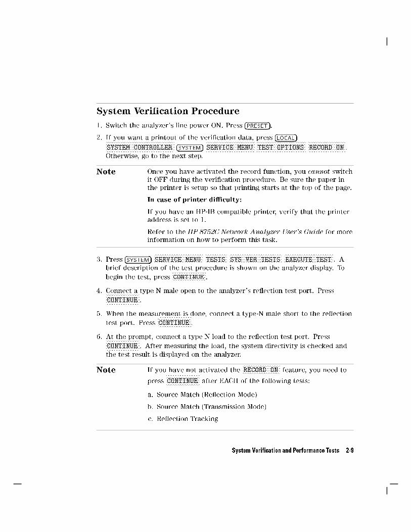
System Veri�cation Procedure
1. Switch the analyzer's line power ON. Press �PRESET�.
2. If you want a printout of the veri�cation data, press �LOCAL�NNNNNNNNNNNNNNNNNNNNNNNNNNNNNNNNNNNNNNNNNNNNNNNNNNNNNSYSTEM CONTROLLER �SYSTEM�
NNNNNNNNNNNNNNNNNNNNNNNNNNNNNNNNNNNNNNSERVICE MENU
NNNNNNNNNNNNNNNNNNNNNNNNNNNNNNNNNNNNNNTEST OPTIONS
NNNNNNNNNNNNNNNNNNNNNNNNNNNNNRECORD ON .
Otherwise, go to the next step.
Note Once you have activated the record function, you cannot switchit OFF during the veri�cation procedure. Be sure the paper inthe printer is setup so that printing starts at the top of the page.
In case of printer di�culty:
If you have an HP-IB compatible printer, verify that the printer
address is set to 1.
Refer to the HP 8752C Network Analyzer User's Guide for moreinformation on how to perform this task.
3. Press �SYSTEM�NNNNNNNNNNNNNNNNNNNNNNNNNNNNNNNNNNNNNNSERVICE MENU
NNNNNNNNNNNNNNNNNTESTS
NNNNNNNNNNNNNNNNNNNNNNNNNNNNNNNNNNNNNNNNNSYS VER TESTS
NNNNNNNNNNNNNNNNNNNNNNNNNNNNNNNNNNNNNNEXECUTE TEST . A
brief description of the test procedure is shown on the analyzer display. To
begin the test, pressNNNNNNNNNNNNNNNNNNNNNNNNNNCONTINUE .
4. Connect a type-N male open to the analyzer's re ection test port. PressNNNNNNNNNNNNNNNNNNNNNNNNNNCONTINUE .
5. When the measurement is done, connect a type-N male short to the re ection
test port. PressNNNNNNNNNNNNNNNNNNNNNNNNNNCONTINUE .
6. At the prompt, connect a type-N load to the re ection test port. PressNNNNNNNNNNNNNNNNNNNNNNNNNNCONTINUE . After measuring the load, the system directivity is checked and
the test result is displayed on the analyzer.
Note If you have not activated theNNNNNNNNNNNNNNNNNNNNNNNNNNNNNRECORD ON feature, you need to
pressNNNNNNNNNNNNNNNNNNNNNNNNNNCONTINUE after EACH of the following tests:
a. Source Match (Re ection Mode)
b. Source Match (Transmission Mode)
c. Re ection Tracking
System Veri�cation and Performance Tests 2-9
7. Connect a type-N RF cable between the analyzer's re ection and
transmission test ports. PressNNNNNNNNNNNNNNNNNNNNNNNNNNCONTINUE to test the system load match.
8. If you have activated the record feature, the system will automatically test
its transmission tracking. Otherwise, pressNNNNNNNNNNNNNNNNNNNNNNNNNNCONTINUE to access this test.
9. PressNNNNNNNNNNNNNNNNNNNNNNNNNNCONTINUE to end the system veri�cation procedure.
In case of di�culty
1. Refer to the \Adjustments and Correction Constants" chapter of this manual.Perform the \Frequency Response Correction Constants Adjustment"
procedure. Repeat the \HP 8752C System Veri�cation" procedure.
2-10 System Veri�cation and Performance Tests

HP 8752C Performance Tests
This portion of the manual contains performance tests which are part of theinstrument calibration process. An instrument calibration includes the systemveri�cation, described in the previous section, and the performance tests.To test the complete set of instrument speci�cations, both portions of theinstrument calibration must be performed.
Note Before performing these performance tests, check that the testequipment is operating to speci�cation. Gage and clean allconnectors.
The following is a list of performance tests in the order in which they should beperformed:
1. Re ection Test Port Output Frequency Range and Accuracy
2. Re ection Test Port Output Power Range and Level Linearity (For HP 8752C
Analyzers without Option 004)
3. Re ection Test Port Output Power Range and Level Linearity (For HP 8752C
Analyzers with Option 004)
4. Transmission Test Port Input Noise Floor Level (For HP 8752C Analyzers
without Option 075)
5. Transmission Test Port Input Noise Floor Level (For HP 8752C Analyzers
with Option 075)
6. Test Port Crosstalk
7. System Trace Noise
8. Magnitude Dynamic Accuracy
9. Phase Dynamic Accuracy
10. Compression
Note Unless otherwise speci�ed, the performance tests are applicableto a standard HP 8752C or an HP 8752C with options.
System Veri�cation and Performance Tests 2-11

Equipment Required to Run the Performance Tests
Description Quantity HP Model or Part Number
Calibration kit, 50 type-N 1 HP 85032B
Calibration kit, 75 type-N 1 HP 85036B1
Measuring Receiver 1 HP 8902A
Frequency counter 1 HP 5343A
Power meter 1 HP 436A, HP 437A, HP 438A
Power sensor 1 HP 8482A
Power sensor 1 HP 8481A2
Power sensor 1 HP 8483A1
Power sensor 1 HP 8483A Option H033
Printer 1 HP ThinkJet, DeskJet,LaserJet
110 dB step attenuator 1 HP 8496A
2-Way power splitter, 50 1 HP 11667A
Cable, 50 type-N 24-inch 3 HP P/N 8120-4781
Cable, 75 type-N 24-inch 2 HP P/N 8120-24081
Minimum Loss Pad 2 HP 11852B1
Adapter type-N(m) to type-N(m) 1 HP P/M 1250-1528
Adapter BNC(m) to N(f) 1 HP P/N 1250-0077
Adapter APC-3.5mm(f) to N(f) 1 HP P/N 1250-1745
1 Required only for instruments with Option 075
2 Required only for instruments with Option 006
3 Required only for instruments with Option 003 and Option 075
2-12 System Veri�cation and Performance Tests
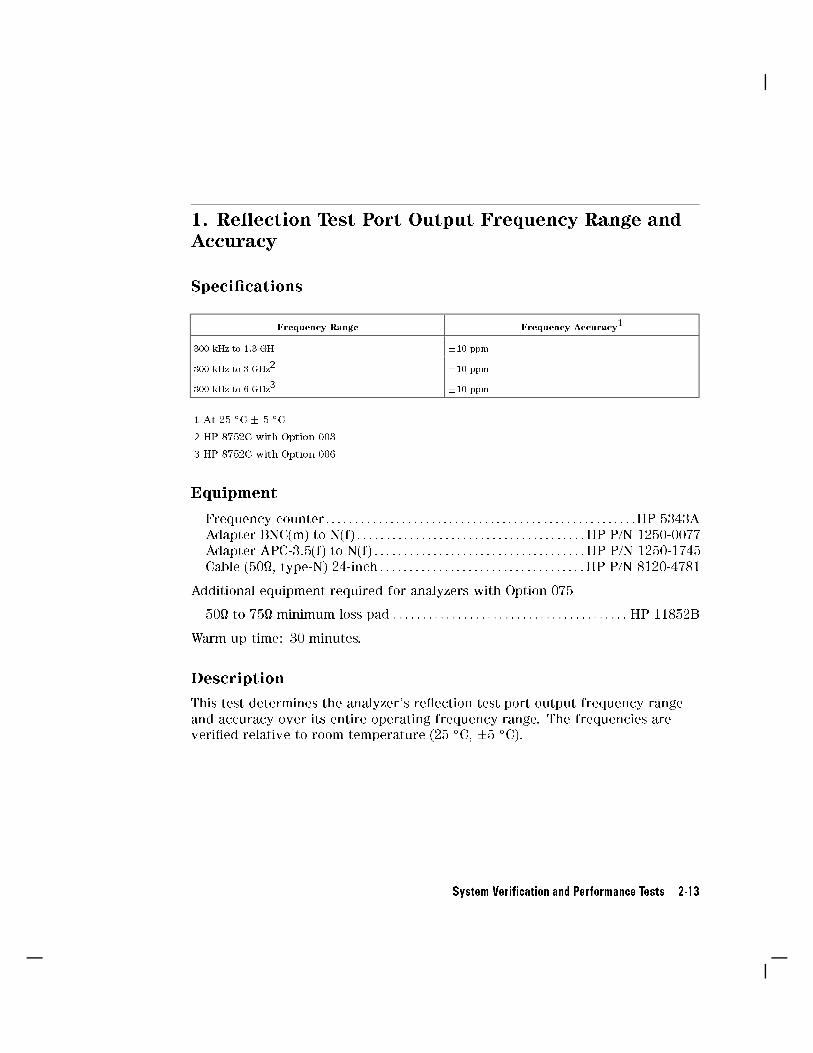
1. Re ection Test Port Output Frequency Range andAccuracy
Speci�cations
Frequency Range Frequency Accuracy1
300 kHz to 1.3 GH �10 ppm
300 kHz to 3 GHz2 �10 ppm
300 kHz to 6 GHz3 �10 ppm
1 At 25 �C � 5 �C
2 HP 8752C with Option 003
3 HP 8752C with Option 006
Equipment
Frequency counter : : : : : : : : : : : : : : : : : : : : : : : : : : : : : : : : : : : : : : : : : : : : : : : : : : : : :HP 5343A
Adapter BNC(m) to N(f) : : : : : : : : : : : : : : : : : : : : : : : : : : : : : : : : : : : : : : :HP P/N 1250-0077
Adapter APC-3.5(f) to N(f) : : : : : : : : : : : : : : : : : : : : : : : : : : : : : : : : : : : :HP P/N 1250-1745
Cable (50, type-N) 24-inch : : : : : : : : : : : : : : : : : : : : : : : : : : : : : : : : : : :HP P/N 8120-4781
Additional equipment required for analyzers with Option 075
50 to 75 minimum loss pad : : : : : : : : : : : : : : : : : : : : : : : : : : : : : : : : : : : : : : : : HP 11852B
Warm-up time: 30 minutes.
Description
This test determines the analyzer's re ection test port output frequency rangeand accuracy over its entire operating frequency range. The frequencies areveri�ed relative to room temperature (25 �C, �5 �C).
System Veri�cation and Performance Tests 2-13

Procedure
1. Connect the equipment as shown in Figure 2-2. Press �PRESET�.
Figure 2-2.Re ection Test Port Output Frequency Range and Accuracy Test Setup
2. Press �MENU�NNNNNNNNNNNNNNNNNNNNNNNCW FREQ �3� �0� �0� �k/m�. Depending on the analyzer's options,
record the frequency counter reading in the appropriate table (2 through 6)in the \Performance Test Record."
3. Repeat step 2 for each instrument's CW frequency listed in the appropriatetable (2 through 6) in the \Performance Test Record."
In case of di�culty
1. If any measured frequency barely fails the speci�cation, check the time base
accuracy of the frequency counter.
2. If the analyzer fails by a signi�cant margin at all frequencies, perform the\Frequency Accuracy" and the \High/Low Band Transition" adjustments.
Refer to the chapter titled \Adjustments and Correction Constants" for more
information on how to perform these adjustment procedures.
3. Refer to the \Source Troubleshooting" chapter in this manual if the problemstill persists.
2-14 System Veri�cation and Performance Tests
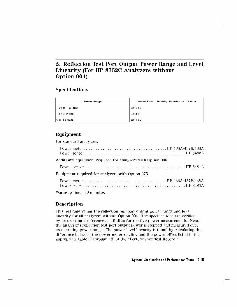
2. Re ection Test Port Output Power Range and LevelLinearity (For HP 8752C Analyzers withoutOption 004)
Speci�cations
Power Range Power Level Linearity Relative to �5 dBm
�20 to �15 dBm �0.5 dB
�15 to 0 dBm �0.2 dB
0 to +5 dBm �0.5 dB
Equipment
For standard analyzers:
Power meter : : : : : : : : : : : : : : : : : : : : : : : : : : : : : : : : : : : : : : : : : : : : : : : :HP 436A/437B/438A
Power sensor : : : : : : : : : : : : : : : : : : : : : : : : : : : : : : : : : : : : : : : : : : : : : : : : : : : : : : : : : : :HP 8482A
Additional equipment required for analyzers with Option 006
Power sensor : : : : : : : : : : : : : : : : : : : : : : : : : : : : : : : : : : : : : : : : : : : : : : : : : : : : : : : : : : :HP 8481A
Equipment required for analyzers with Option 075
Power meter : : : : : : : : : : : : : : : : : : : : : : : : : : : : : : : : : : : : : : : : : : : : : : : :HP 436A/437B/438A
Power sensor : : : : : : : : : : : : : : : : : : : : : : : : : : : : : : : : : : : : : : : : : : : : : : : : : : : : : : : : : : :HP 8483A
Warm-up time: 30 minutes.
Description
This test determines the re ection test port output power range and levellinearity for all analyzers without Option 004. The speci�cations are veri�edby �rst setting a reference at �5 dBm for relative power measurements. Next,the analyzer's re ection test port output power is stepped and measured overits operating power range. The power level linearity is found by calculating thedi�erence between the power meter reading and the power o�set listed in the
appropriate table (7 through 13) of the \Performance Test Record."
System Veri�cation and Performance Tests 2-15

Procedure
Power Range and Level Linearity for an HP 8752C or an HP 8752COption 075
1. Connect the equipment as shown in Figure 2-3.
Note For instruments with Option 075:
a. use an HP 8483A (75) power sensor
b. use tables 11 through 13 in the \Performance Test Record."
For instruments with Option 075 and Option 003, use anHP 8483A Option H03 (75) power sensor.
Figure 2-3.Re ection Test Port Output Power Range and Level Linearity Test Setup
2. Zero and calibrate the power meter. For more information on how toperform this task, refer to the power meter Operating and Service manual.
3. Press �PRESET� �MENU�NNNNNNNNNNNNNNNNNNNNNNNCW FREQ �3� �0� �0� �k/m�.
4. PressNNNNNNNNNNNNNNNNNPOWER ��� �5� �x1�. Set the power meter cal factor for this CW
frequency. On the power meter, set the current power level as the
reference for relative power (dB) measurements. This can be done by
2-16 System Veri�cation and Performance Tests

pressing �dB REF� on an HP 436A or �REL� on an HP 438A power meter frontpanel.
5. PressNNNNNNNNNNNNNNNNNPOWER ��� �2� �0� �x1�. Record the power meter reading in the \Results
Measured" column on the \Performance Test Record."
6. Utilizing the Power O�set value listed in the \Performance Test Record,"calculate the test port output power level linearity using the followingformula:
Power Level Linearity = Measured Value + Power O�set
7. Record the result of your calculation on the \Performance Test Record."
8. Repeat steps 5, 6, and 7 for the other power levels listed in the \HP 8752CPerformance Test Record (7 of 28)."
9. Press �MENU�NNNNNNNNNNNNNNNNNNNNNNNCW FREQ �1� �.� �3� �G/n�.
10. PressNNNNNNNNNNNNNNNNNPOWER ��� �5� �x1�. Set the power meter cal factor for this CW
frequency. Press the appropriate hardkey (�dB REF� or �REL�) on theHP 436A/438A power meter front panel for relative power measurements.
11. Repeat steps 5, 6, and 7 for the other power levels listed in the \HP 8752CPerformance Test Record (8 of 28)."
12. This completes the \Re ection Test Port Output Power Range and LevelLinearity" test if you are working with either a standard analyzer or ananalyzer with only Option 075. Otherwise, go to the appropriate section
below to continue the re ection test port performance tests for other
options.
Power Range and Level Linearity for an HP 8752C with Option 003
13. Press �MENU�NNNNNNNNNNNNNNNNNNNNNNNCW FREQ �3� �G/n�.
14. PressNNNNNNNNNNNNNNNNNPOWER ��� �5� �x1�. Set the power meter cal factor for this CW
frequency. Press the appropriate softkey (�dB REF� or �REL�) on the power
meter front panel for relative power measurements.
15. PressNNNNNNNNNNNNNNNNNPOWER ��� �2� �0� �x1�. Record the power meter reading in the
\Measured Value" column on the \HP 8752C Performance Test Record
(9 of 28)."
System Veri�cation and Performance Tests 2-17

16. Utilizing the Power O�set value listed in the \Performance Test Record(9 of 28)," calculate the Power Level Linearity using the following formula:
Power Level Linearity = Measured Value + Power O�set
17. Record the result of your calculation on the \Performance Test Record(9 of 28)."
18. Repeat steps 15, 16, and 17 for the other power levels listed in the\Performance Test Record (9 of 28)."
Power Range and Level Linearity for an HP 8752C with Options 003and 075
19. Press �MENU�NNNNNNNNNNNNNNNNNNNNNNNCW FREQ �2� �G/n�.
20. Perform steps 14, 15, 16, and 17 for the power levels listed in the
\Performance Test Record (12 of 28)."
Power Range and Level Linearity for an HP 8752C with Option 006
21. Press �MENU�NNNNNNNNNNNNNNNNNNNNNNNCW FREQ �6� �G/n�.
22. Perform steps 14, 15, 16, 17, and 18 for the power levels listed in the
\Performance Test Record (10 of 28)."
In case of di�culty
1. If you cannot set the test port power at any power level, be sure the
analyzer's source power is activated. To do so, press �MENU�NNNNNNNNNNNNNNNNNPOWER . Check
theNNNNNNNNNNNNNNNNNNNNNNNNNNNNNNNNSOURCE PWR softkey. ON should be highlighted.
2. Refer to the \Adjustments and Correction Constants" chapter in this manual.Perform the \RF Output Power Correction Constants Adjustment" procedure.
3. If the problem still exists, refer to the \Source Troubleshooting" chapter inthis manual for more troubleshooting information.
2-18 System Veri�cation and Performance Tests

3. Re ection Test Port Output Power Range and LevelLinearity (HP 8752C with Option 004)
Speci�cations
HP 8752C Option Power Range Power Level Linearity1
Option 004 �85 to +10 dBm �0.2 dB (�15 to +5 dBm)
�0.5 dB (+5 to +10 dBm)
Options 004 and 075 �85 to +8 dBm �0.2 dB (�15 to +5 dBm)
�0.5 dB (+5 to +8 dBm)
1 Relative to �5 dBm
Equipment
For standard analyzers:
Power meter : : : : : : : : : : : : : : : : : : : : : : : : : : : : : : : : : : : : : : : : : : : : : : : : :HP436A/437B/438A
Power sensor : : : : : : : : : : : : : : : : : : : : : : : : : : : : : : : : : : : : : : : : : : : : : : : : : : : : : : : : : : :HP 8482ACable (50, type-N) 24-inch : : : : : : : : : : : : : : : : : : : : : : : : : : : : : : : : : : :HP P/N 1250-1745
Additional equipment required for analyzers with Option 006
Power sensor : : : : : : : : : : : : : : : : : : : : : : : : : : : : : : : : : : : : : : : : : : : : : : : : : : : : : : : : : : :HP 8481A
Equipment required for analyzers with Option 075
Power meter : : : : : : : : : : : : : : : : : : : : : : : : : : : : : : : : : : : : : : : : : : : : : : : : :HP436A/437B/438A
Power sensor : : : : : : : : : : : : : : : : : : : : : : : : : : : : : : : : : : : : : : : : : : : : : : : : : : : : : : : : : : :HP 8483ACable (75, type-N) 24-inch : : : : : : : : : : : : : : : : : : : : : : : : : : : : : : : : : : :HP P/N 8120-2408
Warm-up time: 30 minutes.
Description
This test determines the re ection test port output power range and levellinearity for an analyzer with Option 004. To verify the analyzer power ranges,
a power level of �10 dBm is �rst selected and normalized. Next, various
power levels in di�erent power ranges are selected and compared to the
speci�cations listed in the \Performance Test Record." The analyzer power levellinearity is con�rmed by �rst setting a reference (at �5 dBm) for relative power
measurements. Next, the analyzer's re ection test port output power is stepped
System Veri�cation and Performance Tests 2-19

and measured over its speci�ed power range. The power level linearity is foundby calculating the di�erence between the power meter reading and the powero�set listed in the \Performance Test Record."
Procedure
Power Range for an HP 8752C with Option 004
1. Connect the equipment as shown in Figure 2-4.
Figure 2-4.Re ection Test Port Output Power Range Test Setup
(HP 8752C Option 004)
2. Press �PRESET� �CH 2� to set the analyzer up for transmission measurements.
3. Press �MENU�NNNNNNNNNNNNNNNNNPOWER
NNNNNNNNNNNNNNNNNNNNNNNNNNNNNNNNNNNNNNNNNPWR RANGE MAN
NNNNNNNNNNNNNNNNNNNNNNNNNNNNNNNNNNNNNNPOWER RANGES
NNNNNNNNNNNNNNNNNNNNNNNNNNNNNNNNNNNNNNNNNNNNNNNNNNNNNNNNNNNNRANGE 0 �15 to +10 . Enter the power level value listed in the
the \Performance Test Record (14 of 28)." For this power range, press ��� �1��0� �x1�.
4. Press �DISPLAY�NNNNNNNNNNNNNNNNNNNNNNNNNNNNNNNNNNNNNDATA!MEMORY
NNNNNNNNNNNNNNNNNNNNNNNNNNDATA/MEM �SCALE REF�
NNNNNNNNNNNNNNNNNNNNNNNNNNNNNSCALE/DIV �.� �5� �x1� to
normalize and scale down the data trace.
5. To activate the analyzer's statistic feature, press �MKR FCTN�NNNNNNNNNNNNNNNNNNNNNNNNNNNNNNNNNNNNNNNNNNNNNNNNNNMARKER MODE MENU
NNNNNNNNNNNNNNNNNNNNNNNNNNSTATS ON .
6. Press �MENU�NNNNNNNNNNNNNNNNNNNNNNNNNNNNNNNNNNNNNNTRIGGER MENU
NNNNNNNNNNNNNNNNNNNNNNNNNNNNNNNNNNNNNNNNNNNNNNNNNNNUMBER of GROUPS �5� �x1�.
2-20 System Veri�cation and Performance Tests

7. When the analyzer �nishes the sweeps, record the data trace mean value(as shown on the upper right-hand corner of the analyzer display) on the\Performance Test Record (14 of 28)."
8. Press �MENU�NNNNNNNNNNNNNNNNNPOWER
NNNNNNNNNNNNNNNNNNNNNNNNNNNNNNNNNNNNNNPOWER RANGES
NNNNNNNNNNNNNNNNNNNNNNNNNNNNNNNNNNNNNNNNNNNNNNNNNNNRANGE 1 �25 to 0 . Enter the power
level value listed in the \Performance Test Record." For this power range,press ��� �2� �0� �x1�.
9. Repeat steps 6, 7 and 8 for the other power ranges listed in the \PerformanceTest Record (14 of 28)."
Power Level Linearity for an HP 8752C with Option 004or an HP 8752C withOptions 004 and 075
1. Connect the equipment as shown in Figure 2-5.
Note For instruments with Option 075:
a. use an HP 8483A (75) power sensor
b. use tables 19 through 21 in the \Performance Test Record."
For instruments with Option 075 and Option 003,
use an HP 8483A Option H03 (75) power sensor.
Figure 2-5.Re ection Test Port Output Power Level Linearity Test Setup
System Veri�cation and Performance Tests 2-21

2. Zero and calibrate the power meter. For more information on how toperform this task, refer to the power meter's Operating and Service manual.
3. Press �PRESET� �MENU�NNNNNNNNNNNNNNNNNNNNNNNCW FREQ �3� �0� �0� �k/m�.
4. PressNNNNNNNNNNNNNNNNNPOWER ��� �5� �x1�. Set the power meter cal factor for this CW
frequency. On the power meter, set the current power level as thereference for relative power (dB) measurements by pressing �dB REF� on anHP 436A or �REL� on an HP 438A power meter's front panel.
5. PressNNNNNNNNNNNNNNNNNPOWER ��� �1� �5� �x1�. Record the power meter reading in the \Results
Measured" column on the \Performance Test Record."
6. Utilizing the Power O�set value listed in the \Performance Test Record,"
calculate the Power Level Linearity using the following formula:
Power Level Linearity = Measured Value + Power O�set
7. Record the result of your calculation on the \Performance Test Record."
8. Repeat steps 5, 6 and 7 for the other power levels listed in the\Performance Test Record."
9. Press �MENU�NNNNNNNNNNNNNNNNNNNNNNNCW FREQ �1� �.� �3� �G/n�.
10. PressNNNNNNNNNNNNNNNNNPOWER ��� �5� �x1�. Set the power meter cal factor for this CW
frequency. Press the appropriate hardkey (�dB REF� or �REL�) on the
HP 436A/438A power meter front panel for relative power measurements.
11. Repeat steps 5, 6, 7 and 8.
12. This completes the \Re ection Test Port Output Power Range and Level
Linearity" test if you are working with either an analyzer Option 004 oran analyzer with Options 004 and 075. Otherwise, go to the appropriate
following section to ensure the re ection test port meets speci�cations atthe extended frequency range.
Power Level Linearity for an HP 8752C with Options 003 and 004
13. Press �MENU�NNNNNNNNNNNNNNNNNNNNNNNCW FREQ �3� �G/n�.
14. PressNNNNNNNNNNNNNNNNNPOWER ��� �5� �x1�. Set the power meter cal factor for this CW
frequency. Press the appropriate hardkey (�dB REF� or �REL�) on the powermeter front panel for relative power measurements.
2-22 System Veri�cation and Performance Tests

15. PressNNNNNNNNNNNNNNNNNPOWER ��� �1� �5� �x1�. Record the power meter reading in the \Results
Measured" column on the \Performance Test Record."
16. Utilizing the Power O�set value listed in the \Performance Test Record,"calculate the Power Level Linearity using the following formula:
Power Level Linearity = Measured Value + Power O�set
17. Record the result of your calculation on the \Performance Test Record."
18. Repeat steps 15, 16 and 17 for the other power levels listed in the\Performance Test Record."
Power Level Linearity for an HP 8752C with Options 004 and 006
19. Press �MENU�NNNNNNNNNNNNNNNNNNNNNNNCW FREQ �6� �G/n�.
20. Repeat steps 14, 15, 16, 17 and 18 for the power levels listed in the\Performance Test Record."
Power Level Linearity for an HP 8752C with Options 003, 004,and 075
21. Press �MENU�NNNNNNNNNNNNNNNNNNNNNNNCW FREQ �2� �G/n�.
22. Perform steps 14, 15, 16, 17 and 18 for the power levels listed in the
\Performance Test Record."
In case of di�culty
1. If you cannot set the test port power at any power level, be sure the
analyzer's source power is activated. To do so, press �MENU�NNNNNNNNNNNNNNNNNPOWER . Check
theNNNNNNNNNNNNNNNNNNNNNNNNNNNNNNNNSOURCE PWR softkey. \ON" should be highlighted.
2. Refer to the \Adjustments and Correction Constants" chapter in this manual.Perform the \RF Output Power Correction Constants Adjustment" procedure.
3. If the problem still exists, refer to the \Source Troubleshooting" chapter in
this manual for more troubleshooting information.
System Veri�cation and Performance Tests 2-23

4. Transmission Test Port Input Noise Floor Level(HP 8752C without Option 075)
Speci�cations
Frequency Range IF Bandwidth Average Noise Floor Level
(Transmission)
300 kHz to 1.3 GHz 3 kHz �90 dBm
300 kHz to 1.3 GHz 10 Hz �110 dBm
300 kHz to 3 GHz1 3 kHz �90 dBm
300 kHz to 3 GHz1 10 Hz �110 dBm
3 GHz to 6 GHz2 3 kHz �85 dBm
3 GHz to 6 GHz2 10 Hz �105 dBm
1 HP 8752C with Option 003
2 HP 8752C with Option 006
Equipment
Calibration kit (50, type-N) : : : : : : : : : : : : : : : : : : : : : : : : : : : : : : : : : : : : : : : : : :HP 85032BCable (50, type-N) 24-inch : : : : : : : : : : : : : : : : : : : : : : : : : : : : : : : : : : :HP P/N 8120-4781
Warm-up time: one hour.
Description
This test determines the analyzer's transmission test port input noise oor level.It is tested at 0 dBm at two di�erent IF bandwidths.
Procedure
Noise Floor Level at 300 kHz to 1.3 GHz (Standard Option), 300 kHzto 3 GHz (Option 003), or 300 kHz to 6 GHz (Option 006) with an IFBW of 3 kHz
1. Connect the equipment as shown in Figure 2-6.
2-24 System Veri�cation and Performance Tests

Figure 2-6.
Transmission Test Port Input Noise Floor Level Test Setup 1
2. Press �PRESET� �MENU�NNNNNNNNNNNNNNNNNPOWER �0� �x1�.
If your analyzer has Option 003, press �STOP� �3� �G/n�.
If your analyzer has Option 006, press �STOP� �6� �G/n�.
3. Press �MEAS�NNNNNNNNNNNNNNNNNNNNNNNNNNNNNNNNNNNINPUT PORTS
NNNNNB �DISPLAY�
NNNNNNNNNNNNNNNNNNNNNNNNNNNNNNNNNNNNNDATA!MEMORY
NNNNNNNNNNNNNNNNNNNNNNNNNNDATA/MEM .
4. Connect the equipment as shown in Figure 2-7.
Figure 2-7.Transmission Test Port Input Noise Floor Level Test Setup 2
System Veri�cation and Performance Tests 2-25

5. If your analyzer has Option 004, press �MENU�NNNNNNNNNNNNNNNNNPOWER ��� �8� �5� �x1� �FORMAT�NNNNNNNNNNNNNNNNNNNNNNN
LIN MAG �SCALE REF�NNNNNNNNNNNNNNNNNNNNNNNNNNNNNAUTOSCALE .
If your analyzer does not have Option 004 installed, press �MENU�NNNNNNNNNNNNNNNNNPOWER ���
�2� �0� �x1� �FORMAT�NNNNNNNNNNNNNNNNNNNNNNNLIN MAG �SCALE REF�
NNNNNNNNNNNNNNNNNNNNNNNNNNNNNAUTOSCALE .
6. Press �MKR FCTN�NNNNNNNNNNNNNNNNNNNNNNNNNNNNNNNNNNNNNNNNNNNNNNNNNNMARKER MODE MENU
NNNNNNNNNNNNNNNNNNNNNNNNNNSTATS ON �MENU�
NNNNNNNNNNNNNNNNNNNNNNNNNNNNNNNNNNNNNNTRIGGER MENUNNNNNNNNNNNNNNNNNNNN
SINGLE .
7. When the trace is settled, record its mean value as shown on the analyzerdisplay.
8. Use the equation:
Power (dBm) = 20 * flog10(linear magnitude mean value)g
to convert the linear magnitude mean value (measured in step 7) to logmagnitude. Record this calculated value on the \Performance Test Record(22 of 28)."
Note If your analyzer has Option 003, then record the valuecalculated during the previous step (step 8) on the \Performance
Test Record" under section HP 8752C Option 003 ONLY.
Noise Floor Level at 300 kHz to 1.3 GHz (Standard Option) or300 kHz to 3 GHz (Option 003) with an IF BW of 10 Hz
9. Press �AVG�NNNNNNNNNNNNNNNNNIF BW �1� �0� �x1� to change the IF bandwidth to 10 Hz.
10. Press �MENU�NNNNNNNNNNNNNNNNNNNNNNNNNNNNNNNNNNNNNNTRIGGER MENU
NNNNNNNNNNNNNNNNNNNNSINGLE .
11. When the sweep is done, record its mean value. Use the equation:
Power (dBm) = 20 * flog10(linear magnitude mean value)g
to convert the linear magnitude mean value to log magnitude. Record this
calculated value on the \Performance Test Record (22 of 28)."
12. This completes the \Transmission Test Port Input Noise Floor Level" test
if you are working with either a standard analyzer or an analyzer with
Option 003. Proceed to the next section if your analyzer has Option 006installed.
2-26 System Veri�cation and Performance Tests

Noise Floor Level at 3 GHz to 6 GHz (Option 006) with an IF BW of10 Hz
13. Press �START� �3� �G/n� �STOP� �6� �G/n�. Connect the equipment as shown inFigure 2-8.
Figure 2-8.Transmission Test Port Input Noise Floor Level Test Setup 1
14. Press �MENU�NNNNNNNNNNNNNNNNNPOWER �0� �x1� �MENU�
NNNNNNNNNNNNNNNNNNNNNNNNNNNNNNNNNNNNNNTRIGGER MENU
NNNNNNNNNNNNNNNNNNNNSINGLE .
15. When the sweep is �nished, press �DISPLAY�NNNNNNNNNNNNNNNNNNNNNNNNNNNNNNNNNNNNNDATA!MEMORY �DATA/MEM�.
Connect the equipment as shown in Figure 2-9.
Figure 2-9.Transmission Test Port Input Noise Floor Level Test Setup 2
System Veri�cation and Performance Tests 2-27

16. If your analyzer has Option 004, press �MENU�NNNNNNNNNNNNNNNNNPOWER ��� �8� �5� �x1� �MENU�NNNNNNNNNNNNNNNNNNNNNNNNNNNNNNNNNNNNNN
TRIGGER MENUNNNNNNNNNNNNNNNNNNNNSINGLE .
If your analyzer does not have Option 004 installed, press �MENU�NNNNNNNNNNNNNNNNNPOWER ���
�2� �0� �x1� �MENU�NNNNNNNNNNNNNNNNNNNNNNNNNNNNNNNNNNNNNNTRIGGER MENU
NNNNNNNNNNNNNNNNNNNNSINGLE .
17. When the measurement is done, record the mean value.
18. Use the equation:
Power (dBm) = 20 * flog10(linear magnitude mean value)g
to convert the linear magnitude mean value (measured in step 17) to logmagnitude. Record this calculated value on the \Performance Test Record(22 of 28)."
Noise Floor Level at 3 GHz to 6 GHz (Option 006) with IF BW of3 kHz
19. Press �AVG�NNNNNNNNNNNNNNNNNIF BW �3� �k/m�.
20. Press �MENU�NNNNNNNNNNNNNNNNNNNNNNNNNNNNNNNNNNNNNNTRIGGER MENU
NNNNNNNNNNNNNNNNNNNNNNNNNNNNNNNNNNNNNNNNNNNNNNNNNNNUMBER of GROUPS �5� �x1�.
21. When the sweeps are �nished, record the mean value as shown on theanalyzer display. Repeat step 18.
In case of di�culty
1. Refer to the \Adjustments and Correction Constants" chapter. Perform the
\ADC Linearity Correction Constants Adjustment" procedure. Rerun the
Transmission Test Port Input Noise Floor Level test.
2. If the Noise Floor Level test still fails, suspect the A10 Digital IF boardassembly.
3. Refer to the \Receiver Troubleshooting" section in this manual for moretroubleshooting information.
2-28 System Veri�cation and Performance Tests
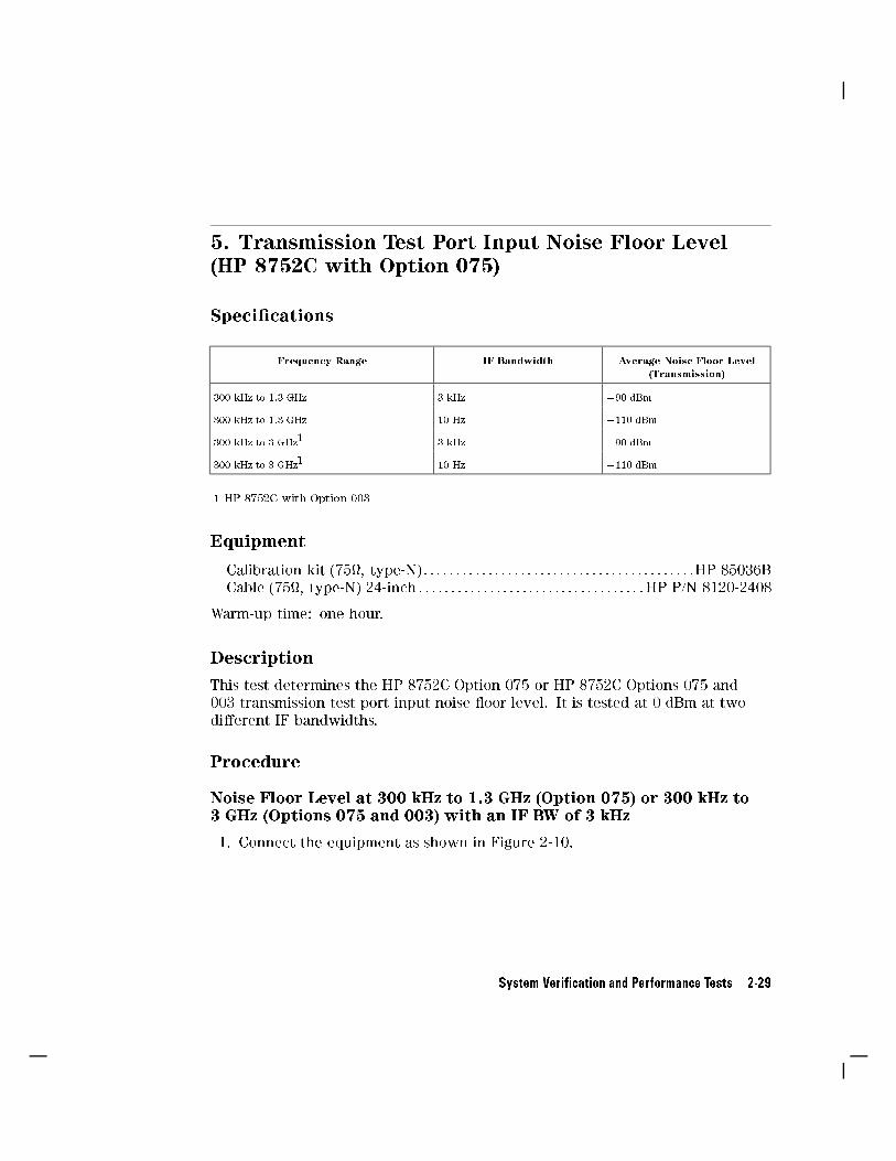
5. Transmission Test Port Input Noise Floor Level(HP 8752C with Option 075)
Speci�cations
Frequency Range IF Bandwidth Average Noise Floor Level
(Transmission)
300 kHz to 1.3 GHz 3 kHz �90 dBm
300 kHz to 1.3 GHz 10 Hz �110 dBm
300 kHz to 3 GHz1 3 kHz �90 dBm
300 kHz to 3 GHz1 10 Hz �110 dBm
1 HP 8752C with Option 003
Equipment
Calibration kit (75, type-N) : : : : : : : : : : : : : : : : : : : : : : : : : : : : : : : : : : : : : : : : : :HP 85036B
Cable (75, type-N) 24-inch : : : : : : : : : : : : : : : : : : : : : : : : : : : : : : : : : : :HP P/N 8120-2408
Warm-up time: one hour.
Description
This test determines the HP 8752C Option 075 or HP 8752C Options 075 and003 transmission test port input noise oor level. It is tested at 0 dBm at twodi�erent IF bandwidths.
Procedure
Noise Floor Level at 300 kHz to 1.3 GHz (Option 075) or 300 kHz to3 GHz (Options 075 and 003) with an IF BW of 3 kHz
1. Connect the equipment as shown in Figure 2-10.
System Veri�cation and Performance Tests 2-29
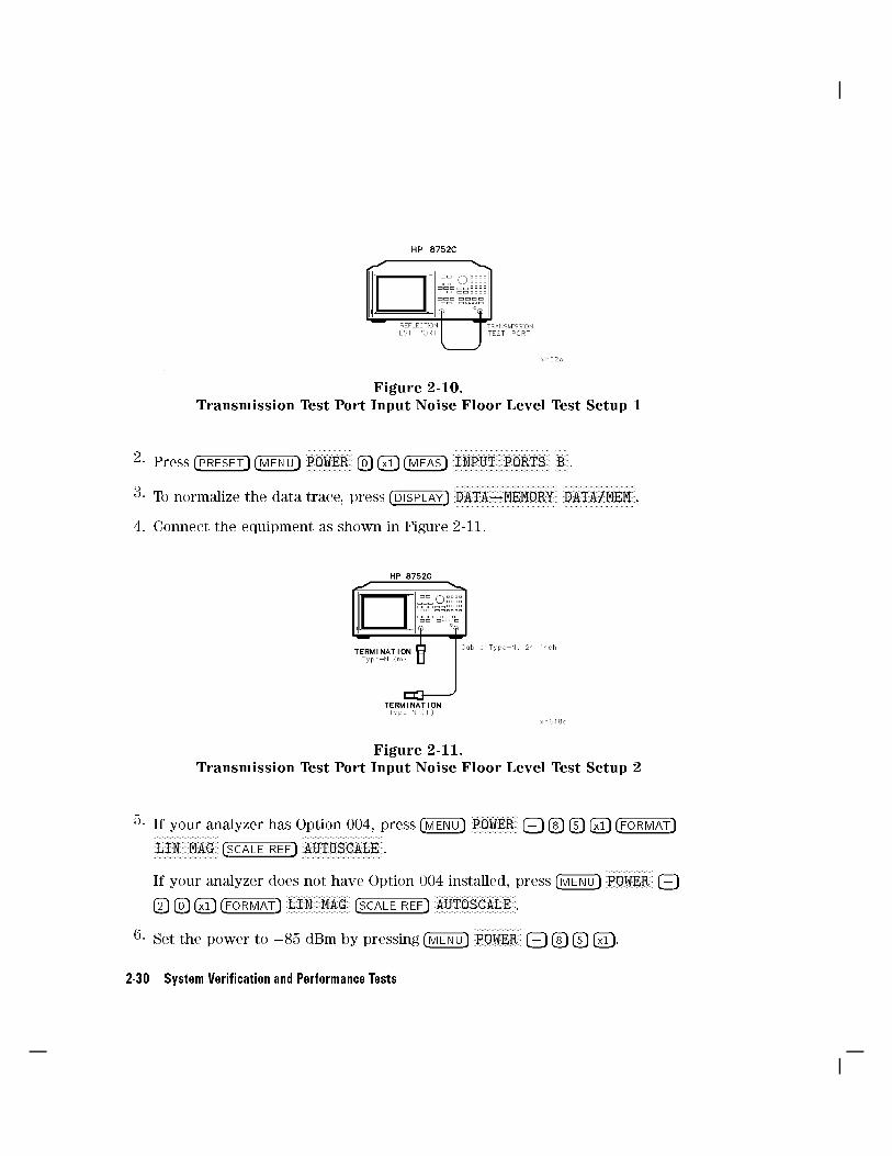
Figure 2-10.
Transmission Test Port Input Noise Floor Level Test Setup 1
2. Press �PRESET� �MENU�NNNNNNNNNNNNNNNNNPOWER �0� �x1� �MEAS�
NNNNNNNNNNNNNNNNNNNNNNNNNNNNNNNNNNNINPUT PORTS
NNNNNB .
3. To normalize the data trace, press �DISPLAY�NNNNNNNNNNNNNNNNNNNNNNNNNNNNNNNNNNNNNDATA!MEMORY
NNNNNNNNNNNNNNNNNNNNNNNNNNDATA/MEM .
4. Connect the equipment as shown in Figure 2-11.
Figure 2-11.Transmission Test Port Input Noise Floor Level Test Setup 2
5. If your analyzer has Option 004, press �MENU�NNNNNNNNNNNNNNNNNPOWER ��� �8� �5� �x1� �FORMAT�NNNNNNNNNNNNNNNNNNNNNNN
LIN MAG �SCALE REF�NNNNNNNNNNNNNNNNNNNNNNNNNNNNNAUTOSCALE .
If your analyzer does not have Option 004 installed, press �MENU�NNNNNNNNNNNNNNNNNPOWER ���
�2� �0� �x1� �FORMAT�NNNNNNNNNNNNNNNNNNNNNNNLIN MAG �SCALE REF�
NNNNNNNNNNNNNNNNNNNNNNNNNNNNNAUTOSCALE .
6. Set the power to �85 dBm by pressing �MENU�NNNNNNNNNNNNNNNNNPOWER ��� �8� �5� �x1�.
2-30 System Veri�cation and Performance Tests

7. Press �MKR FCTN�NNNNNNNNNNNNNNNNNNNNNNNNNNNNNNNNNNNNNNNNNNNNNNNNNNMARKER MODE MENU
NNNNNNNNNNNNNNNNNNNNNNNNNNSTATS ON �MENU�
NNNNNNNNNNNNNNNNNNNNNNNNNNNNNNNNNNNNNNTRIGGER MENU
NNNNNNNNNNNNNNNNNNNNNNNNNNNNNNNNNNNNNNNNNNNNNNNNNNNUMBER of GROUPS �5� �x1�.
8. When the trace is settled, record its mean value (as shown on the analyzer'sdisplay).
9. Use the equation:
Power (dBm) = 20 * flog10(linear magnitude mean value)g
to convert the linear magnitude mean value (measured in step 8) to logmagnitude. Record this calculated value on the \Performance Test Record(23 of 28)."
Note If your analyzer has Option 003, then record the value foundin step 9 on the \Performance Test Record (23 of 28)" under
section HP 8752C Options 075 and 003 ONLY.
Noise Floor Level at 300 kHz to 1.3 GHz (Option 075) or 300 kHz to3 GHz (Options 075 and 003) with an IF BW of 10 Hz
10. Press �AVG�NNNNNNNNNNNNNNNNNIF BW �1� �0� �x1� to change the IF bandwidth to 10 Hz.
11. Press �MENU�NNNNNNNNNNNNNNNNNNNNNNNNNNNNNNNNNNNNNNTRIGGER MENU
NNNNNNNNNNNNNNNNNNNNSINGLE .
12. When the sweep is done, record its mean value. Use the equation:
Power (dBm) = 20 * flog10 (linear magnitude mean value)g
to convert the linear magnitude mean value to log magnitude. Record this
calculated value on the \Performance Test Record (23 of 28)."
In case of di�culty
1. Refer to the \Adjustments and Correction Constants" chapter. Perform the\ADC Linearity Correction Constants Adjustment" procedure. Rerun the
Transmission Test Port Input Noise Floor Level test.
2. If this test still fails, suspect the A10 Digital IF board assembly.
3. Refer to the \Receiver Troubleshooting" section in this manual for moretroubleshooting information.
System Veri�cation and Performance Tests 2-31

6. Test Port Crosstalk
Speci�cations
Frequency Range Test Port Impedance Test Port Crosstalk
300 kHz to 1.3 GHz 50 100 dB
300 kHz to 3 GHz1 50 100 dB
3 GHz to 6 GHz2 50 90 dB
300 kHz to 1.3 GHz 75 100 dB
1.3 GHz to 3 GHz3 75 97 dB
1 HP 8752C with Option 003
2 HP 8752C with Option 006
3 HP 8752C with Option 003 and 075
Equipment
For analyzers without Option 075:
Calibration kit (50, type-N) : : : : : : : : : : : : : : : : : : : : : : : : : : : : : : : : : : : : : : : : : :HP 85032B
For analyzers with Option 075
Calibration kit (75, type-N) : : : : : : : : : : : : : : : : : : : : : : : : : : : : : : : : : : : : : : : : : :HP 85036B
Warm-up time: one hour.
Description
This test veri�es the signal leakage interference between the analyzer re ectionand transmission test ports. The system crosstalk is checked by driving there ection test port and measuring the transmission test port simultaneously.
2-32 System Veri�cation and Performance Tests

Procedure
1. Connect the equipment as shown in Figure 2-12.
Figure 2-12. Test Port Crosstalk Test Setup
2. Depending on the options that are currently installed in your analyzer, go tothe appropriate following section to test the system crosstalk.
Test Port Crosstalk for a Standard HP 8752C or an HP 8752C withOption 003
1. Press �PRESET� �MEAS�NNNNNNNNNNNNNNNNNNNNNNNNNNNNNNNNTRANSMISSN . To set the test port power to 0 dBm,
press �MENU�NNNNNNNNNNNNNNNNNPOWER �0� �x1�.
2. Press �SCALE REF� �2� �5� �x1� �AVG�NNNNNNNNNNNNNNNNNIF BW �1� �0� �x1�
NNNNNNNNNNNNNNNNNNNNNNNNNNNNNNNNNNNNNNNNNNNNNNNNNNAVERAGING FACTOR �5� �x1�NNNNNNNNNNNNNNNNNNNNNNNNNNNNNNNNNNNNNN
AVERAGING ON .
3. Press �MKR FCTN�NNNNNNNNNNNNNNNNNNNNNNNNNNNNNNNNNNNNNNNNNMRK SEARCH ON
NNNNNNNNNNNNNNNNNNNNNNNNNNNNNNNNNNNTRACKING ON
NNNNNNNNNNNNNNNNNNNNNNNNNNNNNNNNSEARCH:MAX .
4. Press �MENU�NNNNNNNNNNNNNNNNNNNNNNNNNNNNNNNNNNNNNNTRIGGER MENU
NNNNNNNNNNNNNNNNNNNNNNNNNNNNNNNNNNNNNNNNNNNNNNNNNNNUMBER of GROUPS �5� �x1�.
5. When the analyzer �nishes sweeping, record the marker value (as shown inthe upper right-hand corner of the analyzer's display) on the appropriatetable in the \Performance Test Record."
Test Port Crosstalk for an HP 8752C with Option 006
1. Press �PRESET� �STOP� �3� �G/n� �MEAS�NNNNNNNNNNNNNNNNNNNNNNNNNNNNNNNNTRANSMISSN . To set the test port power
to 0 dBm, press �MENU�NNNNNNNNNNNNNNNNNPOWER �0� �x1�.
System Veri�cation and Performance Tests 2-33

2. Press �SCALE REF� �2� �5� �x1� �AVG�NNNNNNNNNNNNNNNNNIF BW �1� �0� �x1�
NNNNNNNNNNNNNNNNNNNNNNNNNNNNNNNNNNNNNNNNNNNNNNNNNNAVERAGING FACTOR �5� �x1�NNNNNNNNNNNNNNNNNNNNNNNNNNNNNNNNNNNNNN
AVERAGING ON .
3. Press �MKR FCTN�NNNNNNNNNNNNNNNNNNNNNNNNNNNNNNNNNNNNNNNNNMRK SEARCH ON
NNNNNNNNNNNNNNNNNNNNNNNNNNNNNNNNNNNTRACKING ON
NNNNNNNNNNNNNNNNNNNNNNNNNNNNNNNNSEARCH:MAX .
4. Press �MENU�NNNNNNNNNNNNNNNNNNNNNNNNNNNNNNNNNNNNNNTRIGGER MENU
NNNNNNNNNNNNNNNNNNNNNNNNNNNNNNNNNNNNNNNNNNNNNNNNNNNUMBER of GROUPS �5� �x1�.
5. When the analyzer �nishes sweeping, record the marker value (as shown inthe upper right-hand corner of the analyzer display) on the appropriate tablein the \Performance Test Record."
6. To verify the analyzer system crosstalk in the extended frequency range,press �START� �3� �G/n� �STOP� �6� �G/n�.
7. Press �MENU�NNNNNNNNNNNNNNNNNNNNNNNNNNNNNNNNNNNNNNTRIGGER MENU
NNNNNNNNNNNNNNNNNNNNNNNNNNNNNNNNNNNNNNNNNNNNNNNNNNNUMBER of GROUPS �5� �x1�.
8. When the analyzer �nishes sweeping, record the marker value (as shown inthe upper right-hand corner of the analyzer display) on the appropriate tablein the \Performance Test Record."
Test Port Crosstalk for an HP 8752C with Option 075
1. Press �PRESET� �MEAS�NNNNNNNNNNNNNNNNNNNNNNNNNNNNNNNNTRANSMISSN . To set the test port power to 0 dBm,
press �MENU�NNNNNNNNNNNNNNNNNPOWER �0� �x1�.
2. Press �SCALE REF� �2� �5� �x1� �AVG�NNNNNNNNNNNNNNNNNIF BW �1� �0� �x1�
NNNNNNNNNNNNNNNNNNNNNNNNNNNNNNNNNNNNNNNNNNNNNNNNNNAVERAGING FACTOR �5� �x1�NNNNNNNNNNNNNNNNNNNNNNNNNNNNNNNNNNNNNN
AVERAGING ON .
3. Press �MKR FCTN�NNNNNNNNNNNNNNNNNNNNNNNNNNNNNNNNNNNNNNNNNMRK SEARCH ON
NNNNNNNNNNNNNNNNNNNNNNNNNNNNNNNNNNNTRACKING ON
NNNNNNNNNNNNNNNNNNNNNNNNNNNNNNNNSEARCH:MAX .
4. Press �MENU�NNNNNNNNNNNNNNNNNNNNNNNNNNNNNNNNNNNNNNTRIGGER MENU
NNNNNNNNNNNNNNNNNNNNNNNNNNNNNNNNNNNNNNNNNNNNNNNNNNNUMBER of GROUPS �5� �x1�.
5. When the analyzer is done sweeping, record the marker value (as shown inthe upper right-hand corner of the analyzer display) on the appropriate tablein the \Performance Test Record."
Test Port Crosstalk for an HP 8752C with Options 003 and 075
1. Press �PRESET� �STOP� �1� �.� �3� �G/n� �MEAS�NNNNNNNNNNNNNNNNNNNNNNNNNNNNNNNNTRANSMISSN . To set the test port
power to 0 dBm, press �MENU�NNNNNNNNNNNNNNNNNPOWER �0� �x1�.
2-34 System Veri�cation and Performance Tests

2. Press �SCALE REF� �2� �5� �x1� �AVG�NNNNNNNNNNNNNNNNNIF BW �1� �0� �x1�
NNNNNNNNNNNNNNNNNNNNNNNNNNNNNNNNNNNNNNNNNNNNNNNNNNAVERAGING FACTOR �5� �x1�NNNNNNNNNNNNNNNNNNNNNNNNNNNNNNNNNNNNNN
AVERAGING ON .
3. Press �MKR FCTN�NNNNNNNNNNNNNNNNNNNNNNNNNNNNNNNNNNNNNNNNNMRK SEARCH ON
NNNNNNNNNNNNNNNNNNNNNNNNNNNNNNNNNNNTRACKING ON
NNNNNNNNNNNNNNNNNNNNNNNNNNNNNNNNSEARCH:MAX .
4. Press �MENU�NNNNNNNNNNNNNNNNNNNNNNNNNNNNNNNNNNNNNNTRIGGER MENU
NNNNNNNNNNNNNNNNNNNNNNNNNNNNNNNNNNNNNNNNNNNNNNNNNNNUMBER of GROUPS �5� �x1�.
5. When the analyzer is done sweeping, record the marker value (as shown inthe upper right-hand corner of the analyzer display) on the appropriate tablein the \Performance Test Record."
6. To verify the analyzer system crosstalk in the extended frequency range,press �START� �1� �.� �3� �G/n� �STOP� �3� �G/n�.
7. Press �MENU�NNNNNNNNNNNNNNNNNNNNNNNNNNNNNNNNNNNNNNTRIGGER MENU
NNNNNNNNNNNNNNNNNNNNNNNNNNNNNNNNNNNNNNNNNNNNNNNNNNNUMBER of GROUPS �5� �x1�.
8. When the analyzer is done sweeping, record the marker value (as shown inthe upper right-hand corner of the analyzer display) on the appropriate tablein the \Performance Test Record."
In case of di�culty
1. Remove the instrument top cover. Using an 8 lb-inch torque wrench, verifythat all semi-rigid cables connected to the sampler/mixer assemblies and the
directional coupler are tight. In addition, tighten any loose screws on the
sampler/mixer assemblies (A4/5/6) and the pulse generator assembly (A7).
Rerun the test.
System Veri�cation and Performance Tests 2-35
7. System Trace Noise
Speci�cations
Frequency
Range
Mode System Trace
Noise
(Magnitude)1
System Trace
Noise
(Phase)1
300 kHz to 1.3 GHz Transmission <0.006 dB rms <0.038� rms
300 kHz to 1.3 GHz Re ection <0.006 dB rms <0.038� rms
300 kHz to 3 GHz2 Transmission <0.006 dB rms <0.038� rms
300 kHz to 3 GHz2 Re ection <0.006 dB rms <0.038� rms
3 GHz to 6 GHz3 Transmission <0.010 dB rms <0.070� rms
3 GHz to 6 GHz3 Re ection <0.010 dB rms <0.070� rms
1 At 0 dBm, 3 kHz IF BW
2 HP 8752C with Option 003
3 HP 8752C with Option 006
Equipment
For analyzers without Option 075:
Calibration kit (50, type-N) : : : : : : : : : : : : : : : : : : : : : : : : : : : : : : : : : : : : : : : : : :HP 85032B
Cable (50, type-N) 24-inch : : : : : : : : : : : : : : : : : : : : : : : : : : : : : : : : : : :HP P/N 8120-4781
For analyzers with Option 075:
Calibration kit (75, type-N) : : : : : : : : : : : : : : : : : : : : : : : : : : : : : : : : : : : : : : : : : :HP 85036B
Cable (75, type-N) 24-inch : : : : : : : : : : : : : : : : : : : : : : : : : : : : : : : : : : :HP P/N 8120-2408
Warm-up time: one hour.
Description
This test measures the system trace noise at a designated CW frequency in boththe transmission and re ection modes. It is performed at the instrument'shighest CW frequency since this is the worse case for the system trace noise.
For an analyzer with Options 003 and 075, a CW frequency of 2 GHz is selectedinstead of 3 GHz.
2-36 System Veri�cation and Performance Tests

Procedure
Re ection Trace Noise (Magnitude)
1. Connect the equipment as shown in Figure 2-13.
Figure 2-13. Re ection Trace Noise Test Setup
2. Press �PRESET� �MENU�NNNNNNNNNNNNNNNNNPOWER �0� �x1� �MENU�
NNNNNNNNNNNNNNNNNNNNNNNNNNNNNNNNNNNNNNNNNNNNNNNNNNNUMBER of POINTS �1� �6� �0� �1�
�x1�.
3. If you are testing a standard analyzer, press �MENU�NNNNNNNNNNNNNNNNNNNNNNNCW FREQ �1� �.� �3�
�G/n�. Otherwise, refer to the following table and choose a CW frequency
according to the speci�ed option(s):
Description CW Frequency
HP 8752C with Option 003 3 GHz
HP 8752C with Option 006 6 GHz
HP 8752C with Option 075 1.3 GHz
HP 8752C with Options 075 and 003 2 GHz
4. To get a better view of the system trace noise, press �SCALE REF�NNNNNNNNNNNNNNNNNNNNNNNNNNNNNAUTOSCALE .
5. Press �MKR FCTN�NNNNNNNNNNNNNNNNNNNNNNNNNNNNNNNNNNNNNNNNNNNNNNNNNNMARKER MODE MENU
NNNNNNNNNNNNNNNNNNNNNNNNNNSTATS ON to activate the instrument
statistics feature.
System Veri�cation and Performance Tests 2-37

6. Press �MENU�NNNNNNNNNNNNNNNNNNNNNNNNNNNNNNNNNNNNNNTRIGGER MENU
NNNNNNNNNNNNNNNNNNNNNNNNNNNNNNNNNNNNNNNNNNNNNNNNNNNUMBER of GROUPS �5� �x1�.
7. When the measurement is done, record the s.dev (standard deviation)value shown in the upper right-hand corner of the analyzer display on the\Performance Test Record."
Re ection Trace Noise (Phase)
8. Press �FORMAT�NNNNNNNNNNNNNNNNNPHASE �SCALE REF�
NNNNNNNNNNNNNNNNNNNNNNNNNNNNNAUTOSCALE .
9. Press �MENU�NNNNNNNNNNNNNNNNNNNNNNNNNNNNNNNNNNNNNNTRIGGER MENU
NNNNNNNNNNNNNNNNNNNNNNNNNNNNNNNNNNNNNNNNNNNNNNNNNNNUMBER of GROUPS �5� �x1�.
10. When the measurement is �nished, record the s.dev (standard deviation)value on the \Performance Test Record."
Transmission Trace Noise (Magnitude)
11. Connect the equipment as shown in Figure 2-14.
Figure 2-14. Transmission Trace Noise Test Setup
12. To switch to the transmission mode, press �MEAS�NNNNNNNNNNNNNNNNNNNNNNNNNNNNNNNNTRANSMISSN .
13. Press �MENU�NNNNNNNNNNNNNNNNNNNNNNNNNNNNNNNNNNNNNNTRIGGER MENU
NNNNNNNNNNNNNNNNNNNNNNNNNNNNNNNNNNNNNNNNNNNNNNNNNNNUMBER of GROUPS �5� �x1� �SCALE REF�NNNNNNNNNNNNNNNNNNNNNNNNNNNNN
AUTOSCALE .
14. When the measurement is �nished, record the s.dev (standard deviation)
value on the \Performance Test Record."
2-38 System Veri�cation and Performance Tests
Transmission Trace Noise (Phase)
15. Press �FORMAT�NNNNNNNNNNNNNNNNNPHASE �SCALE REF�
NNNNNNNNNNNNNNNNNNNNNNNNNNNNNAUTOSCALE .
16. Press �MENU�NNNNNNNNNNNNNNNNNNNNNNNNNNNNNNNNNNNNNNTRIGGER MENU
NNNNNNNNNNNNNNNNNNNNNNNNNNNNNNNNNNNNNNNNNNNNNNNNNNNUMBER of GROUPS �5� �x1�.
17. When the measurement is done, record the s. dev (standard deviation) valueon the \Performance Test Record."
In case of di�culty
1. Replace the A10 digital IF board assembly. Rerun the test.
System Veri�cation and Performance Tests 2-39

8. Magnitude Dynamic Accuracy(HP 8752C - All Options)
Speci�cations
Equipment
Measuring receiver: : : : : : : : : : : : : : : : : : : : : : : : : : : : : : : : : : : : : : : : : : : : : : : : : : : : :HP 8902A110 dB step attenuator : : : : : : : : : : : : : : : : : : : : : : : : : : : : : : : : : : : : : : : : : : : : : : : : HP 8496A
Adapter N(m) to N(m) : : : : : : : : : : : : : : : : : : : : : : : : : : : : : : : : : : : : : : : : :HP P/N 1250-1528
50 2-way power splitter : : : : : : : : : : : : : : : : : : : : : : : : : : : : : : : : : : : : : : : : : : : : :HP 11667A
Cable (50, type-N) 24-inch (3 required) : : : : : : : : : : : : : : : : : : : : : :HP P/N 8120-4781
Additional equipment required for analyzers with Option 075:
50 to 75 minimum loss pad (2 required) : : : : : : : : : : : : : : : : : : : : : : : : : : :HP 11852B
Warm-up time: 1 hour
2-40 System Veri�cation and Performance Tests

Description
This test veri�es the magnitude dynamic accuracy of the analyzer's transmissiontest port. The test is performed at a CW frequency of 30 MHz.
Procedure
1. On the HP 8902A, press the blue shift key and �INSTR PRESET� �CLEAR�. Pressthe yellow shift key and �TUNED RF LEVEL�. Press �LOG/LIN� to have theHP 8902A display linear readings (dBm). Press �3� �2� �.� �1� �SPCL�.
2. Set the HP 8496A to 20 dB.
3. On the analyzer, press �PRESET� �MENU�NNNNNNNNNNNNNNNNNNNNNNNCW FREQ �3� �0� �M/��. PressNNNNNNNNNNNNNNNNNNNNNNNNNNNNNNNNNNNNNNNNNNNNNNNNNNNNN
NUMBER of POINTS �5� �1� �x1�. Press �AVG�NNNNNNNNNNNNNNNNNIF BW �1� �0� �x1�.
4. Connect the equipment as shown in Figure 2-15.
System Veri�cation and Performance Tests 2-41
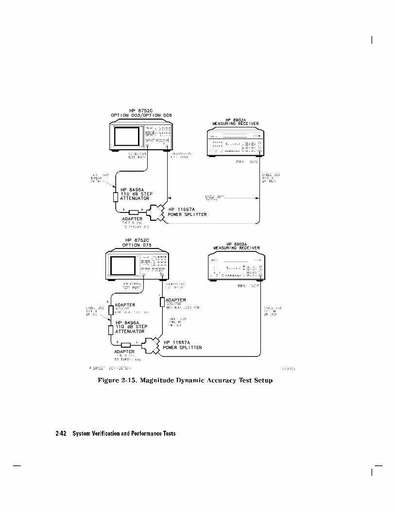
Figure 2-15. Magnitude Dynamic Accuracy Test Setup
2-42 System Veri�cation and Performance Tests

5. On the analyzer, press �MEAS�NNNNNNNNNNNNNNNNNNNNNNNNNNNNNNNNTRANSMISSN �MENU�
NNNNNNNNNNNNNNNNNPOWER �0� �x1�. Using the
analyzer's front panel knob, adjust the test port power for a reading of�30.000 dBm on the HP 8902A. Wait for the reading to stabilize.
Note Ignore the UNCAL annunciation on the HP 8902A.
6. On the HP 8902A, press the blue shift key and �SET REF�.
7. On the analyzer, press �CAL�NNNNNNNNNNNNNNNNNNNNNNNNNNNNNNNNNNNNNNNNNNNNCALIBRATE MENU
NNNNNNNNNNNNNNNNNNNNNNNNNNRESPONSE
NNNNNNNNNNNNNNTHRU . After the
beep, pressNNNNNNNNNNNNNNNNNNNNNNNNNNNNNNNNNNNNNNNNNNNNDONE: RESPONSE .
8. On the analyzer, press �SAVE/RECALL�NNNNNNNNNNNNNNNNNNNNNNNNNNNNNNNNSAVE STATE . Press �MKR FCTN�NNNNNNNNNNNNNNNNNNNNNNNNNNNNNNNNNNNNNNNNNNNNNNNNNN
MARKER MODE MENUNNNNNNNNNNNNNNNNNNNNNNNNNNSTATS ON .
9. Set the HP 8496A to 10 dB.
10. On the analyzer, press �MENU�NNNNNNNNNNNNNNNNNNNNNNNNNNNNNNNNNNNNNNTRIGGER MENU
NNNNNNNNNNNNNNNNNNNNSINGLE .
11. Record the mean value (as shown on the analyzer's display) in the \Trans.
Port" column of the \Performance Test Record."
12. Record the HP 8902A readout in the \HP 8902A" column of the\Performance Test Record."
13. Calculate the di�erence between the \Trans. Port" and the \HP 8902A."
Take the absolute value of this di�erence and enter the result in the\Calculated Value" column of the \Performance Test Record."
14. Set the HP 8496A to the next attenuation setting listed in the \Performance
Test Record." On the analyzer, pressNNNNNNNNNNNNNNNNNNNNSINGLE . Repeat steps 11 to 14 for the
remaining attenuation settings listed in the \Performance Test Record."
Note When the HP 8902A displays the RECAL annunciation, press�CALIBRATE�.
System Veri�cation and Performance Tests 2-43
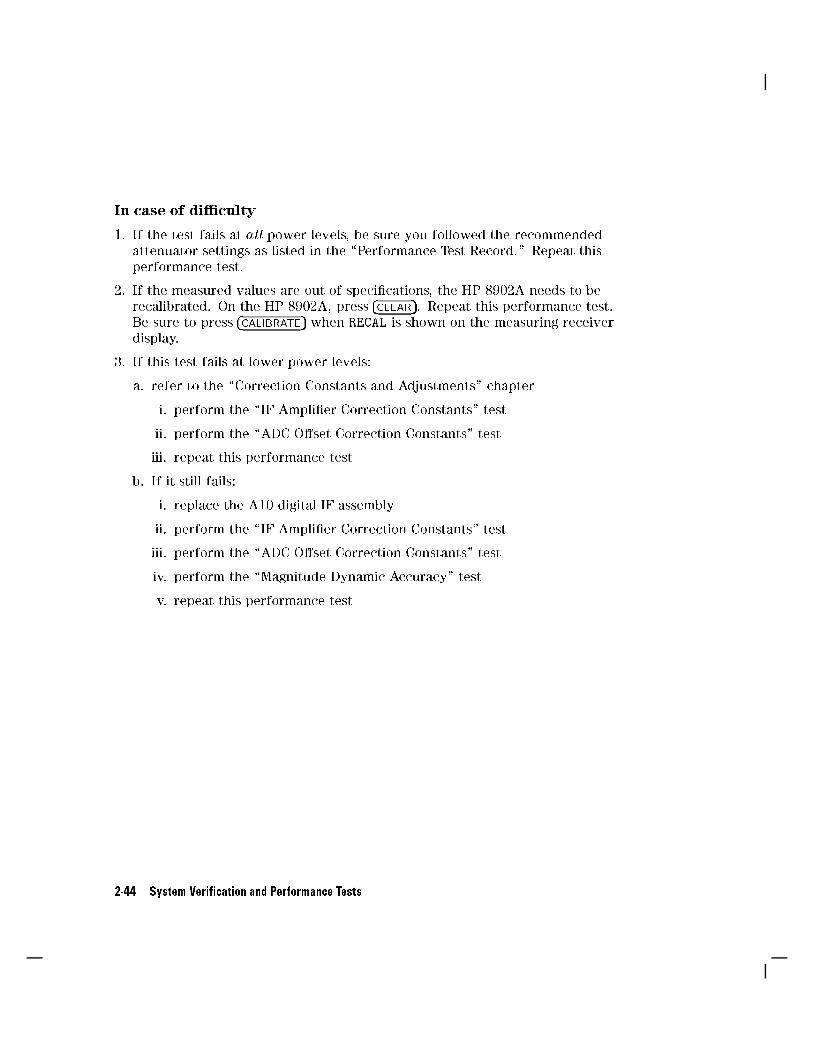
In case of di�culty
1. If the test fails at all power levels, be sure you followed the recommendedattenuator settings as listed in the \Performance Test Record." Repeat thisperformance test.
2. If the measured values are out of speci�cations, the HP 8902A needs to berecalibrated. On the HP 8902A, press �CLEAR�. Repeat this performance test.Be sure to press �CALIBRATE� when RECAL is shown on the measuring receiver
display.
3. If this test fails at lower power levels:
a. refer to the \Correction Constants and Adjustments" chapter
i. perform the \IF Ampli�er Correction Constants" test
ii. perform the \ADC O�set Correction Constants" test
iii. repeat this performance test
b. If it still fails:
i. replace the A10 digital IF assembly
ii. perform the \IF Ampli�er Correction Constants" test
iii. perform the \ADC O�set Correction Constants" test
iv. perform the \Magnitude Dynamic Accuracy" test
v. repeat this performance test
2-44 System Veri�cation and Performance Tests

9. Phase Dynamic Accuracy (HP 8752C - All Options)
Speci�cations
Equipment
There are no external equipment requirements to perform this test.
Description
This test veri�es the phase dynamic accuracy of the analyzer's transmissionport. The test is performed at a CW frequency of 30 MHz.
System Veri�cation and Performance Tests 2-45

Procedure
1. Refer to the \Magnitude Dynamic Accuracy" section of the \Performance TestRecord." For every Trans. Input Power, copy the result from the \CalculatedValue" column and enter it in the \Magnitude Dynamic Accuracy Value"column of the Phase Dynamic Accuracy section of the \Performance TestRecord."
2. For every Trans. Input Power, calculate \A" using the following formula:
A = 10(Magnitude Dynamic Accuracy Value/20)
3. Write the result in the \A" column of the \Performance Test Record."
4. For every Trans. Input Power, calculate \B" using the following formula:
B = 1 � A
5. Write the result in the \B" column of the \Performance Test Record."
6. For every Trans. Input Power, calculate the phase dynamic accuracy, using
the following formula:
Phase Dynamic Accuracy = SIN�1 (B)
7. Write the result in the Calculated Value column of the \Performance TestRecord."
2-46 System Veri�cation and Performance Tests

10. Compression
Speci�cations
Frequency Range Magnitude1 Phase1
300 kHz to 1.3 GHz �0.45 dB �4.2�
1.3 GHz to 3 GHz2 �0.45 dB �4.2�
3 GHz to 6 GHz3 �0.82 dB �5.0�
1 10 Hz IF BW
2 HP 8752C with Option 003
3 HP 8752C with Option 006
Equipment
HP 8752C or HP 8752C Option 003 or HP 8752C Option 006:
Cable (50, type-N) 24-inch : : : : : : : : : : : : : : : : : : : : : : : : : : : : : : : : : : :HP P/N 8120-4781
HP 8752C Option 075:
Cable (75, type-N) 24-inch : : : : : : : : : : : : : : : : : : : : : : : : : : : : : : : : : : :HP P/N 8120-2408
Warm-up time: 1 hour.
Description
This test veri�es the compression/expansion levels of the analyzer's transmissiontest port sampler. Due to their frequency dependent characteristics, thecompression test is performed at selected CW frequencies.
System Veri�cation and Performance Tests 2-47

Procedure
1. Connect the equipment as shown in Figure 2-16.
Figure 2-16. Compression Test Setup
2. Press �PRESET� �MEAS�NNNNNNNNNNNNNNNNNNNNNNNNNNNNNNNNTRANSMISSN .
3. Press �AVG�NNNNNNNNNNNNNNNNNIF BW �1� �0� �x1�.
4. Press �MENU�NNNNNNNNNNNNNNNNNNNNNNNCW FREQ �5� �0� �M/��.
5. PressNNNNNNNNNNNNNNNNNNNNNNNNNNNNNNNNNNNNNNNNNNNNNNNSWEEP TYPE MENU
NNNNNNNNNNNNNNNNNNNNNNNNNNNNNNNNNNNPOWER SWEEP �START� ��� �2� �0� �x1�
�STOP� �0� �x1�.
6. Press �MENU�NNNNNNNNNNNNNNNNNNNNNNNNNNNNNNNNNNNNNNTRIGGER MENU
NNNNNNNNNNNNNNNNNNNNSINGLE .
7. At the end of the sweep, press �SCALE REF�NNNNNNNNNNNNNNNNNNNNNNNNNNNNNAUTOSCALE .
8. Press �MKR FCTN�NNNNNNNNNNNNNNNNNNNNNNNNNNNNNNNNMKR SEARCH
NNNNNNNNNNNNNNNNNNNNNNNNNNNNNNNNNNNSEARCH: MAX .
9. Press �MKR�NNNNNNNNNNNNNNNNNNNNNNNNNNMARKER 2 �MKR FCTN�
NNNNNNNNNNNNNNNNNNNNNNNNNNNNNNNNMKR SEARCH
NNNNNNNNNNNNNNNNNNNNNNNNNNNNNNNNNNNSEARCH: MIN .
10. Press �MKR�NNNNNNNNNNNNNNNNNNNNNNNNNNNNNNNNNNN� MODE MENU
NNNNNNNNNNNNNNNNNNNNNNN� REF=1 .
11. Record the absolute delta value of the (marker 2 � marker 1) reading from
the upper right top-most value in the \Magnitude Value" column of the
\Performance Test Record."
12. Press �FORMAT�NNNNNNNNNNNNNNNNNPHASE .
2-48 System Veri�cation and Performance Tests
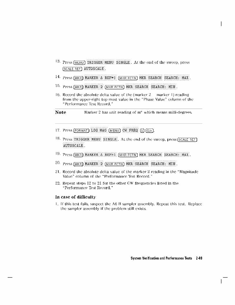
13. Press �MENU�NNNNNNNNNNNNNNNNNNNNNNNNNNNNNNNNNNNNNNTRIGGER MENU
NNNNNNNNNNNNNNNNNNNNSINGLE . At the end of the sweep, press
�SCALE REF�NNNNNNNNNNNNNNNNNNNNNNNNNNNNNAUTOSCALE .
14. Press �MKR�NNNNNNNNNNNNNNNNNNNNNNNNNNNNNNNNNNNNNNNNNNNNMARKER � REF=1 �MKR FCTN�
NNNNNNNNNNNNNNNNNNNNNNNNNNNNNNNNMKR SEARCH
NNNNNNNNNNNNNNNNNNNNNNNNNNNNNNNNNNNSEARCH: MAX .
15. Press �MKR�NNNNNNNNNNNNNNNNNNNNNNNNNNMARKER 2 �MKR FCTN�
NNNNNNNNNNNNNNNNNNNNNNNNNNNNNNNNMKR SEARCH
NNNNNNNNNNNNNNNNNNNNNNNNNNNNNNNNNNNSEARCH: MIN .
16. Record the absolute delta value of the (marker 2 � marker 1) readingfrom the upper-right top most value in the \Phase Value" column of the\Performance Test Record."
Note Marker 2 has unit reading of m� which means milli-degrees.
17. Press �FORMAT�NNNNNNNNNNNNNNNNNNNNNNNLOG MAG �MENU�
NNNNNNNNNNNNNNNNNNNNNNNCW FREQ �1� �G/n�.
18. PressNNNNNNNNNNNNNNNNNNNNNNNNNNNNNNNNNNNNNNTRIGGER MENU
NNNNNNNNNNNNNNNNNNNNSINGLE . At the end of the sweep, press �SCALE REF�NNNNNNNNNNNNNNNNNNNNNNNNNNNNN
AUTOSCALE .
19. Press �MKR�NNNNNNNNNNNNNNNNNNNNNNNNNNNNNNNNNNNNNNNNNNNNMARKER � REF=1 �MKR FCTN�
NNNNNNNNNNNNNNNNNNNNNNNNNNNNNNNNMKR SEARCH
NNNNNNNNNNNNNNNNNNNNNNNNNNNNNNNNNNNSEARCH: MAX .
20. Press �MKR�NNNNNNNNNNNNNNNNNNNNNNNNNNMARKER 2 �MKR FCTN�
NNNNNNNNNNNNNNNNNNNNNNNNNNNNNNNNMKR SEARCH
NNNNNNNNNNNNNNNNNNNNNNNNNNNNNNNNNNNSEARCH: MIN .
21. Record the absolute delta value of the marker 2 reading in the \MagnitudeValue" column of the \Performance Test Record."
22. Repeat steps 12 to 21 for the other CW frequencies listed in the\Performance Test Record."
In case of di�culty
1. If this test fails, suspect the A6 B sampler assembly. Repeat this test. Replacethe sampler assembly if the problem still exists.
System Veri�cation and Performance Tests 2-49
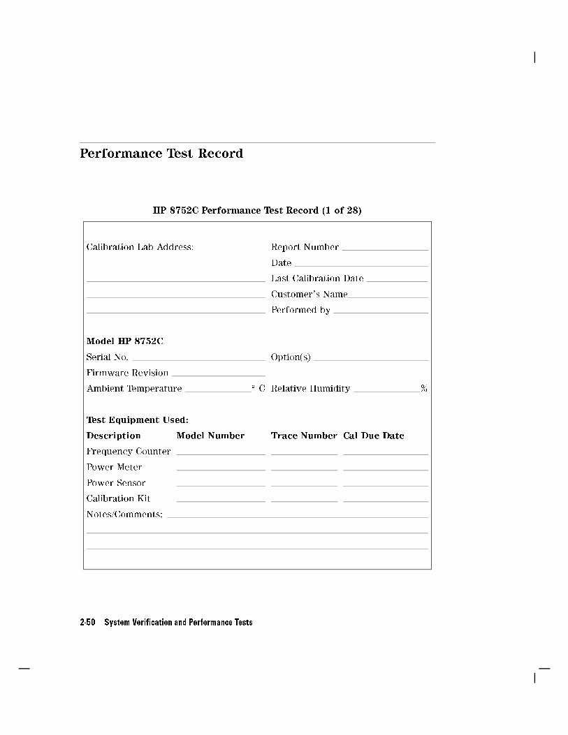
Performance Test Record
HP 8752C Performance Test Record (1 of 28)
Calibration Lab Address: Report Number
Date
Last Calibration Date
Customer's Name
Performed by
Model HP 8752C
Serial No. Option(s)
Firmware Revision
Ambient Temperature � C Relative Humidity %
Test Equipment Used:
Description Model Number Trace Number Cal Due Date
Frequency Counter
Power Meter
Power Sensor
Calibration Kit
Notes/Comments:
2-50 System Veri�cation and Performance Tests

HP 8752C Performance Test Record (2 of 28)
Hewlett-Packard Company
Model HP 8752C Report Number
Serial Number Date
� � 1. Re ection Test Port Output Frequency Range and Accuracy (Standard HP 8752C)
CW Frequencies
(MHz)
Min.
(MHz)
Results Measured
(MHz)
Max.
(MHz)
Measurement
Uncertainty
(MHz)
0.3 0.299 997 0.300 003 � 0.000 000 360
5.0 4.999 950 5.000 050 � 0.000 006
16.0 15.999 840 16.000 160 � 0.000 019
31.0 30.999 690 31.000 310 � 0.000 037
60.999 999 60.999 390 61.000 610 � 0.000 073
121.0 120.998 790 121.001 210 � 0.000 145
180.0 179.998 200 180.001 800 � 0.000 216
310.0 309.995 900 310.003 100 � 0.000 372
700.0 699.930 000 700.007 000 � 0.000 840
1 300.0 1 299.987 000 1 300.013 � 0.001 560
System Veri�cation and Performance Tests 2-51

HP 8752C Performance Test Record (3 of 28)
Hewlett-Packard Company
Model HP 8752C Report Number
Serial Number Date
� � 1. Re ection Test Port Output Frequency Range and Accuracy
(HP 8752C Option 003)
CW Frequencies
(MHz)
Min.
(MHz)
Results Measured
(MHz)
Max.
(MHz)
Measurement
Uncertainty
(MHz)
0.3 0.299 997 0.300 003 � 0.000 000 360
5.0 4.999 950 5.000 050 � 0.000 006
16.0 15.999 840 16.000 160 � 0.000 019
31.0 30.999 690 31.000 310 � 0.000 037
60.999 999 60.999 390 61.000 610 � 0.000 073
121.0 120.998 790 121.001 210 � 0.000 145
180.0 179.998 200 180.001 800 � 0.000 216
310.0 309.995 900 310.003 100 � 0.000 372
700.0 699.930 000 700.007 000 � 0.000 840
1 300.0 1 299.987 000 1 300.013 � 0.001 560
2 000.0 1 999.980 000 2 000.020 000 � 0.002 400
3 000.0 2 999.970 000 3 000.030 000 � 0.003 600
2-52 System Veri�cation and Performance Tests

HP 8752C Performance Test Record (4 of 28)
Hewlett-Packard Company
Model HP 8752C Report Number
Serial Number Date
� � 1. Re ection Test Port Output Frequency Range and Accuracy
(HP 8752C Option 006)
CW Frequencies
(MHz)
Min.
(MHz)
Results Measured
(MHz)
Max.
(MHz)
Measurement
Uncertainty
(MHz)
0.3 0.299 997 0.300 003 � 0.000 000 360
5.0 4.999 950 5.000 050 � 0.000 006
16.0 15.999 840 16.000 160 � 0.000 019
31.0 30.999 690 31.000 310 � 0.000 037
60.999 999 60.999 390 61.000 610 � 0.000 073
121.0 120.998 790 121.001 210 � 0.000 145
180.0 179.998 200 180.001 800 � 0.000 216
310.0 309.995 900 310.003 100 � 0.000 372
700.0 699.930 000 700.007 000 � 0.000 840
1 300.0 1 299.987 000 1 300.013 � 0.001 560
2 000.0 1 999.980 000 2 000.020 000 � 0.002 400
3 000.0 2 999.970 000 3 000.030 000 � 0.003 600
4 000.0 3 999.960 4 000.040 � 0.004 800
5 000.0 4 999.950 5 000.050 � 0.006 000
6 000.0 5 999.940 6 000.060 � 0.007 200
System Veri�cation and Performance Tests 2-53

HP 8752C Performance Test Record (5 of 28)
Hewlett-Packard Company
Model HP 8752C Report Number
Serial Number Date
� � 1. Re ection Test Port Output Frequency Range and Accuracy
(HP 8752C Option 075)
CW Frequencies
(MHz)
Min.
(MHz)
Results Measured
(MHz)
Max.
(MHz)
Measurement
Uncertainty
(MHz)
0.3 0.299 997 0.300 003 � 0.000 000 360
5.0 4.999 950 5.000 050 � 0.000 006
16.0 15.999 840 16.000 160 � 0.000 019
31.0 30.999 690 31.000 310 � 0.000 037
60.999 999 60.999 390 61.000 610 � 0.000 073
121.0 120.998 790 121.001 210 � 0.000 145
180.0 179.998 200 180.001 800 � 0.000 216
310.0 309.995 900 310.003 100 � 0.000 372
700.0 699.930 000 700.007 000 � 0.000 840
1 300.0 1 299.987 000 1 300.013 � 0.001 560
2-54 System Veri�cation and Performance Tests

HP 8752C Performance Test Record (6 of 28)
Hewlett-Packard Company
Model HP 8752C Report Number
Serial Number Date
� � 1. Re ection Test Port Output Frequency Range and Accuracy
(HP 8752C Options 003 and 075)
CW Frequencies
(MHz)
Min.
(MHz)
Results Measured
(MHz)
Max.
(MHz)
Measurement
Uncertainty
(MHz)
0.3 0.299 997 0.300 003 � 0.000 000 360
5.0 4.999 950 5.000 050 � 0.000 006
16.0 15.999 840 16.000 160 � 0.000 019
31.0 30.999 690 31.000 310 � 0.000 037
60.999 999 60.999 390 61.000 610 � 0.000 073
121.0 120.998 790 121.001 210 � 0.000 145
180.0 179.998 200 180.001 800 � 0.000 216
310.0 309.995 900 310.003 100 � 0.000 372
700.0 699.930 000 700.007 000 � 0.000 840
1 300.0 1 299.987 000 1 300.013 � 0.001 560
2 000.0 1 999.980 000 2 000.020 000 � 0.002 400
3 000.0 2 999.970 000 3 000.030 000 � 0.003 600
System Veri�cation and Performance Tests 2-55
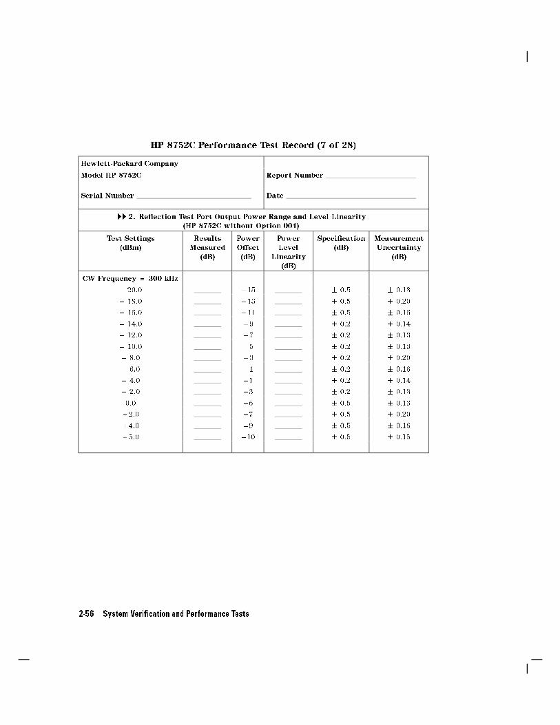
HP 8752C Performance Test Record (7 of 28)
Hewlett-Packard Company
Model HP 8752C Report Number
Serial Number Date
� � 2. Re ection Test Port Output Power Range and Level Linearity
(HP 8752C without Option 004)
Test Settings
(dBm)
Results
Measured
(dB)
Power
O�set
(dB)
Power
Level
Linearity
(dB)
Speci�cation
(dB)
Measurement
Uncertainty
(dB)
CW Frequency = 300 kHz
� 20.0 +15 � 0.5 � 0.13
� 18.0 +13 � 0.5 � 0.20
� 16.0 +11 � 0.5 � 0.16
� 14.0 +9 � 0.2 � 0.14
� 12.0 +7 � 0.2 � 0.13
� 10.0 +5 � 0.2 � 0.13
� 8.0 +3 � 0.2 � 0.20
� 6.0 +1 � 0.2 � 0.16
� 4.0 �1 � 0.2 � 0.14
� 2.0 �3 � 0.2 � 0.13
0.0 �5 � 0.5 � 0.13
+2.0 �7 � 0.5 � 0.20
+4.0 �9 � 0.5 � 0.16
+5.0 �10 � 0.5 � 0.15
2-56 System Veri�cation and Performance Tests

HP 8752C Performance Test Record (8 of 28)
Hewlett-Packard Company
Model HP 8752C Report Number
Serial Number Date
� � 2. Re ection Test Port Output Power Range and Level Linearity
(HP 8752C without Option 004)
Test Settings
(dBm)
Results
Measured
(dB)
Power
O�set
(dB)
Power
Level
Linearity
(dB)
Speci�cation
(dB)
Measurement
Uncertainty
(dB)
CW Frequency = 1.3 GHz
�20.0 +15 �0.5 �0.23
�18.0 +13 �0.5 �0.15
�16.0 +11 �0.5 �0.01
�14.0 +9 �0.2 �0.06
�12.0 +7 �0.2 �0.07
�10.0 +5 �0.2 �0.09
�8.0 +3 �0.2 �0.06
�6.0 +1 �0.2 �0.03
�4.0 �1 �0.2 �0.02
�2.0 �3 �0.2 �0.01
0.0 �5 �0.5 �0.09
+2.0 �7 �0.5 �0.06
+4.0 �9 �0.5 �0.03
+5.0 �10 �0.5 �0.03
System Veri�cation and Performance Tests 2-57

HP 8752C Performance Test Record (9 of 28)
Hewlett-Packard Company
Model HP 8752C Report Number
Serial Number Date
� � 2. Re ection Test Port Output Power Range and Level Linearity
(HP 8752C with Option 003, without Option 004)
Test Settings
(dBm)
Results
Measured
(dB)
Power
O�set
(dB)
Power
Level
Linearity
(dB)
Speci�cation
(dB)
Measurement
Uncertainty
(dB)
CW Frequency = 3.0 GHz
�20.0 +15 �0.5 �0.23
�18.0 +13 �0.5 �0.15
�16.0 +11 �0.5 �0.01
�14.0 +9 �0.2 �0.06
�12.0 +7 �0.2 �0.07
�10.0 +5 �0.2 �0.09
�8.0 +3 �0.2 �0.06
�6.0 +1 �0.2 �0.03
�4.0 �1 �0.2 �0.02
�2.0 �3 �0.2 �0.01
0.0 �5 �0.5 �0.09
+2.0 �7 �0.5 �0.06
+4.0 �9 �0.5 �0.03
+5.0 �10 �0.5 �0.03
2-58 System Veri�cation and Performance Tests

HP 8752C Performance Test Record (10 of 28)
Hewlett-Packard Company
Model HP 8752C Report Number
Serial Number Date
� � 2. Re ection Test Port Output Power Range and Level Linearity
(HP 8752C with Option 006, without Option 004)
Test Settings
(dBm)
Results
Measured
(dB)
Power
O�set
(dB)
Power
Level
Linearity
(dB)
Speci�cation
(dB)
Measurement
Uncertainty
(dB)
CW Frequency = 6.0 GHz
�20.0 +15 �0.5 �0.23
�18.0 +13 �0.5 �0.15
�16.0 +11 �0.5 �0.01
�14.0 +9 �0.2 �0.06
�12.0 +7 �0.2 �0.07
�10.0 +5 �0.2 �0.09
�8.0 +3 �0.2 �0.06
�6.0 +1 �0.2 �0.03
�4.0 �1 �0.2 �0.02
�2.0 �3 �0.2 �0.01
0.0 �5 �0.5 �0.09
+2.0 �7 �0.5 �0.06
+4.0 �9 �0.5 �0.03
+5.0 �10 �0.5 �0.03
System Veri�cation and Performance Tests 2-59

HP 8752C Performance Test Record (11 of 28)
Hewlett-Packard Company
Model HP 8752C Report Number
Serial Number Date
� � 2. Re ection Test Port Output Power Range and Level Linearity
(HP 8752C with Option 075, without Option 004)
Test Settings
(dBm)
Results
Measured
(dB)
Power
O�set
(dB)
Power
Level
Linearity
(dB)
Speci�cation
(dB)
Measurement
Uncertainty
(dB)
CW Frequency = 300 kHz
�20.0 +15 �0.5 �0.13
�18.0 +13 �0.5 �0.20
�16.0 +11 �0.5 �0.16
�14.0 +9 �0.2 �0.14
�12.0 +7 �0.2 �0.13
�10.0 +5 �0.2 �0.13
�8.0 +3 �0.2 �0.20
�6.0 +1 �0.2 �0.16
�4.0 �1 �0.2 �0.14
�2.0 �3 �0.2 �0.13
0.0 �5 �0.5 �0.13
+2.0 �7 �0.5 �0.20
+4.0 �9 �0.5 �0.16
+5.0 �10 � 0.5 �0.15
2-60 System Veri�cation and Performance Tests

HP 8752C Performance Test Record (12 of 28)
Hewlett-Packard Company
Model HP 8752C Report Number
Serial Number Date
� � 2. Re ection Test Port Output Power Range and Level Linearity
(HP 8752C with Option 075, without Option 004)
Test Settings
(dBm)
Results
Measured
(dB)
Power
O�set
(dB)
Power
Level
Linearity
(dB)
Speci�cation
(dB)
Measurement
Uncertainty
(dB)
CW Frequency = 1.3 GHz
�20.0 +15 �0.5 �0.13
�18.0 +13 �0.5 �0.20
�16.0 +11 �0.5 �0.16
�14.0 +9 �0.2 �0.14
�12.0 +7 �0.2 �0.13
�10.0 +5 �0.2 �0.13
�8.0 +3 �0.2 �0.20
�6.0 +1 �0.2 �0.16
�4.0 �1 �0.2 �0.14
�2.0 �3 �0.2 �0.13
0.0 �5 �0.5 �0.13
+2.0 �7 � 0.5 �0.20
+4.0 �9 � 0.5 �0.16
+5.0 �10 � 0.5 �0.15
System Veri�cation and Performance Tests 2-61

HP 8752C Performance Test Record (13 of 28)
Hewlett-Packard Company
Model HP 8752C Report Number
Serial Number Date
� � 2. Re ection Test Port Output Power Range and Level Linearity
(HP 8752C with Options 003 and 075, without Option 004)
Test Settings
(dBm)
Results
Measured
(dB)
Power
O�set
(dB)
Power
Level
Linearity
(dB)
Speci�cation
(dB)
Measurement
Uncertainty
(dB)
CW Frequency = 2 GHz
�20.0 +15 �0.5 �0.13
�18.0 +13 �0.5 �0.20
�16.0 +11 �0.5 �0.16
�14.0 +9 �0.2 �0.14
�12.0 +7 �0.2 �0.13
�10.0 +5 �0.2 �0.13
�8.0 +3 �0.2 �0.20
�6.0 +1 �0.2 �0.16
�4.0 �1 �0.2 �0.14
�2.0 �3 �0.2 �0.13
0.0 �5 �0.5 �0.13
+2.0 �7 �0.5 �0.20
+4.0 �9 �0.5 �0.16
+5.0 �10 �0.5 �0.15
2-62 System Veri�cation and Performance Tests

HP 8752C Performance Test Record (14 of 28)
Hewlett-Packard Company
Model HP 8752C Report Number
Serial Number Date
� � 3. Re ection Test Port Output Power Range (HP 8752C with Option 004)
Power Range
(dBm)
Power Level
Value
(dB)
Speci�cation
(dB)
Mean Value
(dB)
Measurement
Uncertainty
(dB)
�15 to +10 �10 0 �1.0 �0.100
�25 to 0 �20 0 �1.5 �0.060
�35 to �10 �30 0 �1.7 �0.050
�45 to �20 �40 0 �1.9 �0.050
�55 to �30 �50 0 �2.2 �0.055
�65 to �40 �60 0 �2.5 �0.080
�75 to �50 �70 0 �2.8 �0.200
�85 to �60 �80 0 �3.1 �0.565
System Veri�cation and Performance Tests 2-63

HP 8752C Performance Test Record (15 of 28)
Hewlett-Packard Company
Model HP 8752C Report Number
Serial Number Date
� � 3. Re ection Test Port Output Power Level Linearity (HP 8752C with Option 004)
Test Settings
(dBm)
Results
Measured
(dB)
Power
O�set
(dB)
Power
Level
Linearity
(dB)
Speci�cation
(dB)
Measurement
Uncertainty
(dB)
CW Frequency = 300 kHz
� 15.0 +10 � 0.2 � 0.06
� 12.0 +7 � 0.2 � 0.07
� 10.0 +5 � 0.2 � 0.09
� 8.0 +3 � 0.2 � 0.06
� 6.0 +1 � 0.2 � 0.03
� 4.0 �1 � 0.2 � 0.02
� 2.0 �3 � 0.2 � 0.01
0.0 �5 � 0.5 � 0.09
+2.0 �7 � 0.5 � 0.06
+4.0 �9 � 0.5 � 0.03
+5.0 �10 � 0.5 � 0.03
+10.0 �15 � 0.5 � 0.03
2-64 System Veri�cation and Performance Tests

HP 8752C Performance Test Record (16 of 28)
Hewlett-Packard Company
Model HP 8752C Report Number
Serial Number Date
� � 3. Re ection Test Port Output Power Level Linearity (HP 8752C with Option 004)
Test Settings
(dBm)
Results
Measured
(dB)
Power
O�set
(dB)
Power
Level
Linearity
(dB)
Speci�cation
(dB)
Measurement
Uncertainty
(dB)
CW Frequency = 1.3 GHz
� 15.0 +10 � 0.2 � 0.06
� 12.0 +7 � 0.2 � 0.07
� 10.0 +5 � 0.2 � 0.09
� 8.0 +3 � 0.2 � 0.06
� 6.0 +1 � 0.2 � 0.03
� 4.0 �1 � 0.2 � 0.02
� 2.0 �3 � 0.2 � 0.01
0.0 �5 � 0.5 � 0.09
+2.0 �7 � 0.5 � 0.06
+4.0 �9 � 0.5 � 0.03
+5.0 �10 � 0.5 � 0.03
+10.0 �15 � 0.5 � 0.03
System Veri�cation and Performance Tests 2-65

HP 8752C Performance Test Record (17 of 28)
Hewlett-Packard Company
Model HP 8752C Report Number
Serial Number Date
� � 3. Re ection Test Port Output Power Level Linearity (HP 8752C with Option 004)
Test Settings
(dBm)
Results
Measured
(dB)
Power
O�set
(dB)
Power
Level
Linearity
(dB)
Speci�cation
(dB)
Measurement
Uncertainty
(dB)
CW Frequency = 3 GHz
� 15.0 +10 � 0.2 � 0.06
� 12.0 +7 � 0.2 � 0.07
� 10.0 +5 � 0.2 � 0.09
� 8.0 +3 � 0.2 � 0.06
� 6.0 +1 � 0.2 � 0.03
� 4.0 �1 � 0.2 � 0.02
� 2.0 �3 � 0.2 � 0.01
0.0 �5 � 0.5 � 0.09
+2.0 �7 � 0.5 � 0.06
+4.0 �9 � 0.5 � 0.03
+5.0 �10 � 0.5 � 0.03
+10.0 �15 � 0.5 � 0.03
2-66 System Veri�cation and Performance Tests

HP 8752C Performance Test Record (18 of 28)
Hewlett-Packard Company
Model HP 8752C Report Number
Serial Number Date
� � 3. Re ection Test Port Output Power Level Linearity
(HP 8752C with Options 004 and 006)
Test Settings
(dBm)
Results
Measured
(dB)
Power
O�set
(dB)
Power
Level
Linearity
(dB)
Speci�cation
(dB)
Measurement
Uncertainty
(dB)
CW Frequency = 6 GHz
� 15.0 +10 � 0.2 � 0.06
� 12.0 +7 � 0.2 � 0.07
� 10.0 +5 � 0.2 � 0.09
� 8.0 +3 � 0.2 � 0.06
� 6.0 +1 � 0.2 � 0.03
� 4.0 �1 � 0.2 � 0.02
� 2.0 �3 � 0.2 � 0.01
0.0 �5 � 0.5 � 0.09
+2.0 �7 � 0.5 � 0.06
+4.0 �9 � 0.5 � 0.03
+5.0 �10 � 0.5 � 0.03
+10.0 �15 � 0.5 � 0.03
System Veri�cation and Performance Tests 2-67

HP 8752C Performance Test Record (19 of 28)
Hewlett-Packard Company
Model HP 8752C Report Number
Serial Number Date
� � 3. Re ection Test Port Output Power Level Linearity
(HP 8752C with Options 004 and 075)
Test Settings
(dBm)
Results
Measured
(dB)
Power
O�set
(dB)
Power
Level
Linearity
(dB)
Speci�cation
(dB)
Measurement
Uncertainty
(dB)
CW Frequency = 300 kHz
� 15.0 +10 � 0.2 � 0.14
� 12.0 +7 � 0.2 � 0.13
� 10.0 +5 � 0.2 � 0.13
� 8.0 +3 � 0.2 � 0.20
� 6.0 +1 � 0.2 � 0.16
� 4.0 �1 � 0.2 � 0.14
� 2.0 �3 � 0.2 � 0.13
0.0 �5 � 0.5 � 0.13
+2.0 �7 � 0.5 � 0.20
+4.0 �9 � 0.5 � 0.16
+5.0 �10 � 0.5 � 0.15
+8.0 �13 � 0.5 � 0.15
2-68 System Veri�cation and Performance Tests
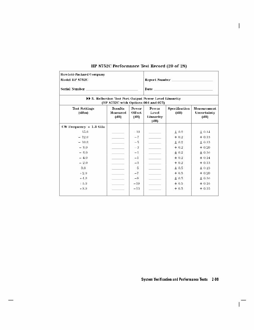
HP 8752C Performance Test Record (20 of 28)
Hewlett-Packard Company
Model HP 8752C Report Number
Serial Number Date
� � 3. Re ection Test Port Output Power Level Linearity
(HP 8752C with Options 004 and 075)
Test Settings
(dBm)
Results
Measured
(dB)
Power
O�set
(dB)
Power
Level
Linearity
(dB)
Speci�cation
(dB)
Measurement
Uncertainty
(dB)
CW Frequency = 1.3 GHz
� 15.0 +10 � 0.2 � 0.14
� 12.0 +7 � 0.2 � 0.13
� 10.0 +5 � 0.2 � 0.13
� 8.0 +3 � 0.2 � 0.20
� 6.0 +1 � 0.2 � 0.16
� 4.0 �1 � 0.2 � 0.14
� 2.0 �3 � 0.2 � 0.13
0.0 �5 � 0.5 � 0.13
+2.0 �7 � 0.5 � 0.20
+4.0 �9 � 0.5 � 0.16
+5.0 �10 � 0.5 � 0.15
+8.0 �13 � 0.5 � 0.15
System Veri�cation and Performance Tests 2-69

HP 8752C Performance Test Record (21 of 28)
Hewlett-Packard Company
Model HP 8752C Report Number
Serial Number Date
� � 3. Re ection Test Port Output Power Level Linearity
(HP 8752C with Options 003, 004, and 075)
Test Settings
(dBm)
Results
Measured
(dB)
Power
O�set
(dB)
Power
Level
Linearity
(dB)
Speci�cation
(dB)
Measurement
Uncertainty
(dB)
CW Frequency = 2 GHz
� 15.0 +10 � 0.2 � 0.14
� 12.0 +7 � 0.2 � 0.13
� 10.0 +5 � 0.2 � 0.13
� 8.0 +3 � 0.2 � 0.20
� 6.0 +1 � 0.2 � 0.16
� 4.0 �1 � 0.2 � 0.14
� 2.0 �3 � 0.2 � 0.13
0.0 �5 � 0.5 � 0.13
+2.0 �7 � 0.5 � 0.20
+4.0 �9 � 0.5 � 0.16
+5.0 �10 � 0.5 � 0.15
+8.0 �13 � 0.5 � 0.15
2-70 System Veri�cation and Performance Tests

HP 8752C Performance Test Record (22 of 28)
Hewlett-Packard Company
Model HP 8752C Report Number
Serial Number Date
� � 4. Transmission Test Port Input Noise Floor Level (HP 8752C without Option 075)
Frequency Range IF BW Speci�cation
(dBm)
Calculated
Value
Measurement
Uncertainty
(dB)
HP 8752C Standard ONLY
300 kHz to 1.3 GHz 3 kHz � 90 N/A
300 kHz to 1.3 GHz 10 Hz � 110 N/A
HP 8752C Option 003 ONLY
300 kHz to 3 GHz 3 kHz � 90 N/A
300 kHz to 3 GHz 10 Hz � 110 N/A
HP 8752C Option 006 ONLY
3 GHz to 6 GHz 3 kHz �85 N/A
3 GHz to 6 GHz 10 Hz �105 N/A
System Veri�cation and Performance Tests 2-71

HP 8752C Performance Test Record (23 of 28)
Hewlett-Packard Company
Model HP 8752C Report Number
Serial Number Date
� � 5. Transmission Test Port Input Noise Floor Level (HP 8752C with Option 075)
Frequency Range IF BW Spec.
(dBm)
Calculated
Value
Measurement
Uncertainty
(dB)
300 kHz to 1.3 GHz 3 kHz � 90 N/A
300 kHz to 1.3 GHz 10 Hz � 110 N/A
HP 8752C Options 075 and 003 ONLY
300 kHz to 3 GHz 3 kHz � 90 N/A
300 kHz to 3 GHz 10 Hz � 110 N/A
2-72 System Veri�cation and Performance Tests
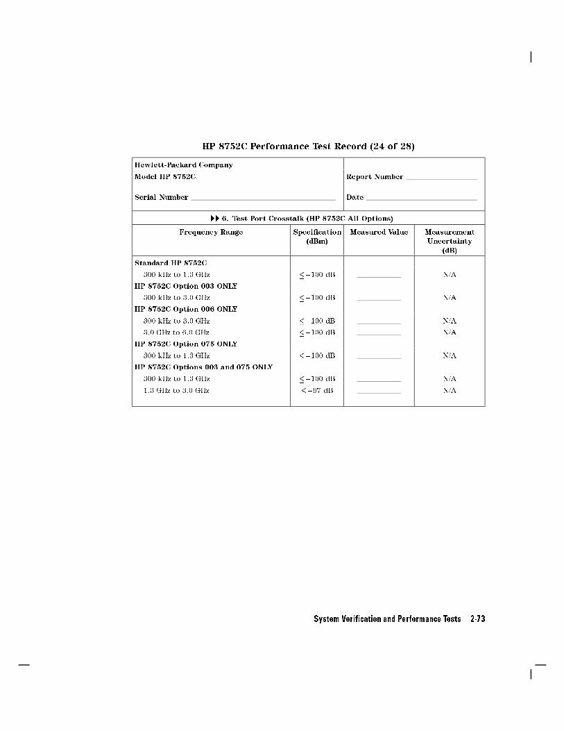
HP 8752C Performance Test Record (24 of 28)
Hewlett-Packard Company
Model HP 8752C Report Number
Serial Number Date
� � 6. Test Port Crosstalk (HP 8752C All Options)
Frequency Range Speci�cation
(dBm)
Measured Value Measurement
Uncertainty
(dB)
Standard HP 8752C
300 kHz to 1.3 GHz ��100 dB N/A
HP 8752C Option 003 ONLY
300 kHz to 3.0 GHz ��100 dB N/A
HP 8752C Option 006 ONLY
300 kHz to 3.0 GHz ��100 dB N/A
3.0 GHz to 6.0 GHz ��100 dB N/A
HP 8752C Option 075 ONLY
300 kHz to 1.3 GHz ��100 dB N/A
HP 8752C Options 003 and 075 ONLY
300 kHz to 1.3 GHz ��100 dB N/A
1.3 GHz to 3.0 GHz ��97 dB N/A
System Veri�cation and Performance Tests 2-73

HP 8752C Performance Test Record (25 of 28)
Hewlett-Packard Company
Model HP 8752C Report Number
Serial Number Date
� � 7. System Trace Noise (HP 8752C All Options)
Mode IF BW Speci�cation
(dBm)
Measured
Value
(dB)
Measurement
Uncertainty
(dB)
Standard HP 8752C
Re ection Magnitude 3 kHz <0.006 dB rms N/A
Re ection Phase 3 kHz <0.038� rms N/A
Transmission Magnitude 3 kHz <0.006 dB rms N/A
Transmission Phase 3 kHz <0.038� rms N/A
HP 8752C Option 003 ONLY
Re ection Magnitude 3 kHz <0.006 dB rms N/A
Re ection Phase 3 kHz <0.038� rms N/A
Transmission Magnitude 3 kHz <0.006 dB rms N/A
Transmission Phase 3 kHz <0.038� rms N/A
HP 8752C Option 006 ONLY
Re ection Magnitude 3 kHz <0.010 dB rms N/A
Re ection Phase 3 kHz <0.070� rms N/A
Transmission Magnitude 3 kHz <0.010 dB rms N/A
Transmission Phase 3 kHz <0.070� rms N/A
HP 8752C Option 075 ONLY
Re ection Magnitude 3 kHz <0.006 dB rms N/A
Re ection Phase 3 kHz <0.038� rms N/A
Transmission Magnitude 3 kHz <0.006 dB rms N/A
Transmission Phase 3 kHz <0.038� rms N/A
HP 8752C Options 003 and 075 ONLY
Re ection Magnitude 3 kHz <0.006 dB rms N/A
Re ection Phase 3 kHz <0.038� rms N/A
Transmission Magnitude 3 kHz <0.006 dB rms N/A
Transmission Phase 3 kHz <0.038� rms N/A
2-74 System Veri�cation and Performance Tests
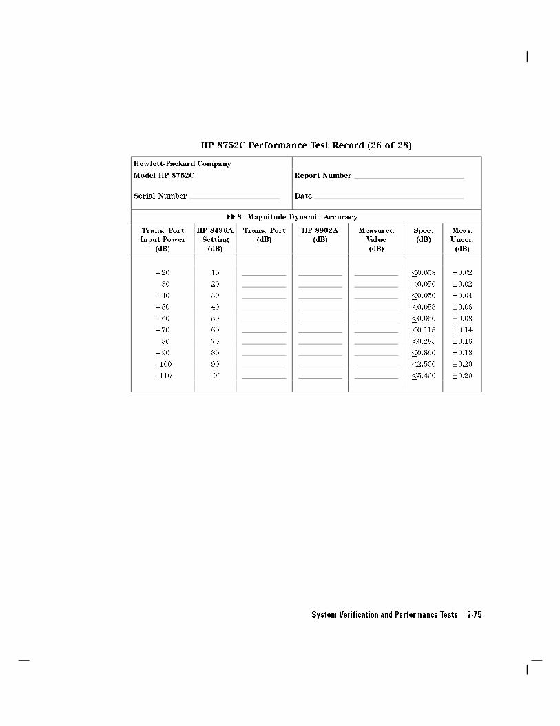
HP 8752C Performance Test Record (26 of 28)
Hewlett-Packard Company
Model HP 8752C Report Number
Serial Number Date
� � 8. Magnitude Dynamic Accuracy
Trans. Port
Input Power
(dB)
HP 8496A
Setting
(dB)
Trans. Port
(dB)
HP 8902A
(dB)
Measured
Value
(dB)
Spec.
(dB)
Meas.
Uncer.
(dB)
�20 10 �0.058 �0.02
�30 20 �0.050 �0.02
�40 30 �0.050 �0.04
�50 40 �0.053 �0.06
�60 50 �0.060 �0.08
�70 60 �0.115 �0.14
�80 70 �0.285 �0.16
�90 80 �0.860 �0.18
�100 90 �2.500 �0.20
�110 100 �5.400 �0.20
System Veri�cation and Performance Tests 2-75

HP 8752C Performance Test Record (27 of 28))
Hewlett-Packard Company
Model HP 8752C Report Number
Serial Number Date
� � 9. Phase Dynamic Accuracy
Trans. Port
Input Power
(dB)
Magnitude
Dynamic
Accuracy
Value
A B Calculated
Value
(degrees)
Spec.
(degrees)
Meas.
Uncert.
�20 �0.46 N/A
�30 �0.35 N/A
�40 �0.36 N/A
�50 �0.38 N/A
�60 �0.40 N/A
�70 �0.70 N/A
�80 �1.90 N/A
�90 �6.00 N/A
�100 �18.00 N/A
�110 �55.00 N/A
2-76 System Veri�cation and Performance Tests

HP 8752C Performance Test Record (28 of 28)
Hewlett-Packard Company
Model HP 8752C Report Number
Serial Number Date
� � 10. Compression
CW
Freq.(GHz)
Magnitude
Value
(dB)
Spec.
(dB)
Meas.
Uncert.
Phase
Value
(degrees)
Spec.
(degrees)
Meas.
Uncer.
(dB)
0.05 �0.45 N/A �4.2 N/A
1.00 �0.45 N/A �4.2 N/A
1.30 �0.45 N/A �4.2 N/A
System Veri�cation and Performance Tests 2-77


3
Adjustments and Correction Constants
The accuracy of the analyzer is achieved and maintained through mechanicaladjustments and correction constants. The correction constants are empiricallyderived data that is stored in memory. Correction constants re�ne the analyzer'smeasurements and de�ne its operation.
When to Perform the Adjustment Procedures
Perform the following adjustment procedures in these two instances:
if one of the analyzer's assemblies has been replaced
orif one or more of the analyzer's performance tests failed.
Keep Correction Constants Current to Save Time
Keep the correction constants current by performing \15. EEPROM BackupDisk Procedure" any time you perform one or more of the correction constantadjustment procedures. Then, if you need to replace the A9 assembly, you canquickly retrieve the data from the back up disk, rather than regenerating it byperforming all of the correction constant adjustment procedures.
Adjustment Procedure Error Messages
POW MET INVALIDPOW MET NOT SETTLEDPOW MET NOT FOUND
The messages listed above indicate power meter problems.
Adjustments and Correction Constants 3-1

If the analyzer displays one of these messages, check:
the test setupthe line powerthe HP-IB connections and addressesthe model number
After the problem has been identi�ed and corrected, repeat the test.
TROUBLE! CHECK SET-UP AND START OVER
Check your setup against the illustrated test setup and repeat the test.
Perform Adjustments in This Order
When performing more than one adjustment, perform them in this order:
1. A9 CC Jumper Position Procedure2. EEPROM Backup Disk Procedure3. Initialize EEPROMs (Test #58)
4. Source Default Correction Constants (Test #44)
5. Source Pretune Default Correction Constants (Test #45)
6. Analog Bus Correction Constants (Test #46)
7. RF Output Power Correction Constants (Test #47)8. Source Pretune Correction Constants (Test #48)
9. Display Intensity Adjustments (Test #49)
10. IF Ampli�er Correction Constants (Test #51)
11. ADC O�set Correction Constants (Test #52)
12. Frequency Response Correction Constants (Tests #57 then #53)13. Cavity Oscillator Correction Constants (Test #54)14. Serial Number Correction Constant (Test #55)15. Option Number Correction Constant (Test #56)16. Model Number Correction Constant17. Vertical Position and Focus Adjustments
18. Display Degaussing (Demagnetizing)19. Fractional-N Frequency Range Adjustment
20. Frequency Accuracy Adjustment
21. High/Low Band Transition Adjustment
22. Fractional-N Spur and FM Sideband Adjustment
23. Source Spur Avoidance Tracking Adjustment24. EEPROM Backup Disk Procedure
3-2 Adjustments and Correction Constants

Note If you have replaced the CPU board, or if the analyzer has lostall of its correction constants perform the adjustments in theorder listed below (from top to bottom):
1. A9 CC Jumper Position Procedure12. Serial Number Correction Constant (Test #55)13. Option Number Correction Constant (Test #56)16. Model Number Correction Constant14. Initialize EEPROMs (Test #58)16. Model Number Correction Constant7. Display Intensity Adjustments (Test #49)17. Vertical Position and Focus Adjustments18. Display Degaussing (Demagnetizing)2. Source Default Correction Constants (Test #44)3. Source Pretune Default Correction Constants (Test #45)
4. Analog Bus Correction Constants (Test #46)
9. ADC O�set Correction Constants (Test #52)
19. Fractional-N Frequency Range Adjustment
6. Source Pretune Correction Constants (Test #48)20. Frequency Accuracy Adjustment
21. High/Low Band Transition Adjustment
22. Fractional-N Spur and FM Sideband Adjustment
23. Source Spur Avoidance Tracking Adjustment
5. RF Output Power Correction Constants (Test #47)8. IF Ampli�er Correction Constants (Test #51)
11. Cavity Oscillator Correction Constants (Test #54)
10. Frequency Response Correction Constants (Tests #57 then
#53)
15. EEPROM Backup Disk Procedure
Test Equipment Speci�cations
Each of the following procedures lists the equipment required to perform theadjustment procedure. Typically, common hand tools (screwdrivers, etc.) are not
listed.
If you do not have the required equipment, refer to the critical speci�cations inTable 1-1 to identify appropriate substitutes.
Adjustments and Correction Constants 3-3

Analyzer Cover Removal
Typically, when performing the analyzer's adjustment procedures, only the topcover needs to be removed (to adjust the A9CC jumper position).
To remove the top cover:
1. Remove the upper rear stando�s.2. Loosen the top cover retaining screw.3. Slide back the cover.
3-4 Adjustments and Correction Constants
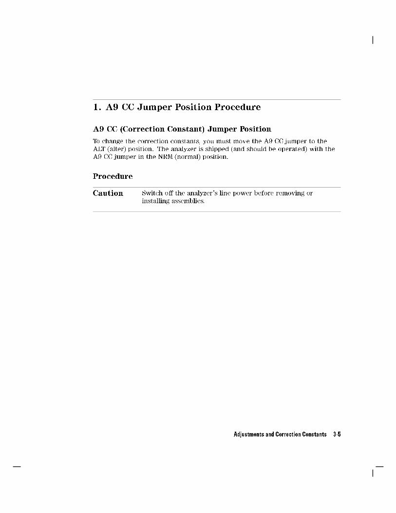
1. A9 CC Jumper Position Procedure
A9 CC (Correction Constant) Jumper Position
To change the correction constants, you must move the A9 CC jumper to theALT (alter) position. The analyzer is shipped (and should be operated) with theA9 CC jumper in the NRM (normal) position.
Procedure
Caution Switch o� the analyzer's line power before removing orinstalling assemblies.
Adjustments and Correction Constants 3-5

Figure 3-1. Location of Major Assemblies
3-6 Adjustments and Correction Constants

1. Remove the analyzer top cover (see the section titled \Analyzer CoverRemoval," located earlier in this chapter).
2. Remove the PC board stabilizer (item 1, Figure 3-1).3. Remove the A9 CPU assembly by pulling on the white lifters.
Figure 3-2. NRM (Normal) and ALT (Alter) Positions of A9 CC Jumper
4. Move the A9 CC jumper to the ALT position. Refer to Figure 3-2.5. Reinstall the A9 assembly and run the correction constant routine(s).6. Return the A9 CC jumper to the NRM position (see \1. A9 CC Jumper
Position Procedure").
Note Update the EEPROM backup disk by performing \15. EEPROMBackup Disk Procedure" at the end of this chapter.
Adjustments and Correction Constants 3-7

2. Source Default Correction Constants (Test #44)
Equipment
No equipment is required to perform this adjustment.
Warm-up time
5 minutes
Description and Procedure
This internal adjustment test writes default correction constants forrudimentary source power accuracy. This adjustment must be performed before
the \Source Pretune Correction Constants (Test #45)" procedure.
1. Put the A9 CC jumper in the ALT position (see \1. A9 CC Jumper Position
Procedure").2. Press �PRESET�.3. Press �SYSTEM�
NNNNNNNNNNNNNNNNNNNNNNNNNNNNNNNNNNNNNNSERVICE MENU
NNNNNNNNNNNNNNNNNTESTS �44� �x1�. When the display shows
*Source Def -ND-
pressNNNNNNNNNNNNNNNNNNNNNNNNNNNNNNNNNNNNNNEXECUTE TEST .
4. PressNNNNNNNNNNNYES at the query to alter the correction constants.
5. When complete, DONE should appear on the display.
6. Refer to \15. EEPROM Backup Disk Procedure" to store the new correctionconstants.
7. Return the A9 CC jumper to the NRM position (see \1. A9 CC JumperPosition Procedure").
3-8 Adjustments and Correction Constants

3. Source Pretune Default Correction Constants(Test #45)
Equipment
No equipment is required to perform this adjustment.
Warm-up time
30 minutes
Description and Procedure
This adjustment generates two default correction constants which pretune theYIG oscillators to insure proper phase lock.
1. Put the A9 CC jumper in the ALT position (see \1. A9 CC Jumper Position
Procedure").2. Press �PRESET�.3. Press �SYSTEM�
NNNNNNNNNNNNNNNNNNNNNNNNNNNNNNNNNNNNNNSERVICE MENU
NNNNNNNNNNNNNNNNNTESTS �45� �x1�.
4. When the analyzer displays
*Pretune Def
pressNNNNNNNNNNNNNNNNNNNNNNNNNNNNNNNNNNNNNNEXECUTE TEST .
5. PressNNNNNNNNNNNYES at the query to alter the correction constants and observe the
display:If *Pretune Def DONE is displayed, the adjustment is complete.
Refer to \15. EEPROM Backup Disk Procedure" to store the newcorrection constants. Return the A9 CC jumper to the NRM position (see\1. A9 CC Jumper Position Procedure").
Adjustments and Correction Constants 3-9

4. Analog Bus Correction Constants (Test #46)
Equipment
No equipment is required for this adjustment.
Warm-up time
30 minutes
Description and Procedure
This procedure calibrates the analog bus using three reference voltages: ground,+0.37V and +2.5V. It then stores the calibration data as correction constants in
EEPROM.
1. Put the A9 CC jumper in the ALT position (see \1. A9 CC Jumper Position
Procedure").2. Press �PRESET�.3. Press �SYSTEM�
NNNNNNNNNNNNNNNNNNNNNNNNNNNNNNNNNNNNNNSERVICE MENU
NNNNNNNNNNNNNNNNNTESTS �46� �x1�. When the display shows:
ABUS Cor
pressNNNNNNNNNNNNNNNNNNNNNNNNNNNNNNNNNNNNNNEXECUTE TEST and then press
NNNNNNNNNNNYES at the query to alter the correction
constants and observe the display:ABUS COR DONE displayed: the adjustment is complete. Refer to \15.
EEPROM Backup Disk Procedure" to store the new correction constants.
Return the A9 CC jumper to the NRM position (see \1. A9 CC JumperPosition Procedure").
ABUS COR FAIL displayed: rerun the procedure; in case of continuedimproper operation, refer to the chapter titled \Digital ControlTroubleshooting."
3-10 Adjustments and Correction Constants
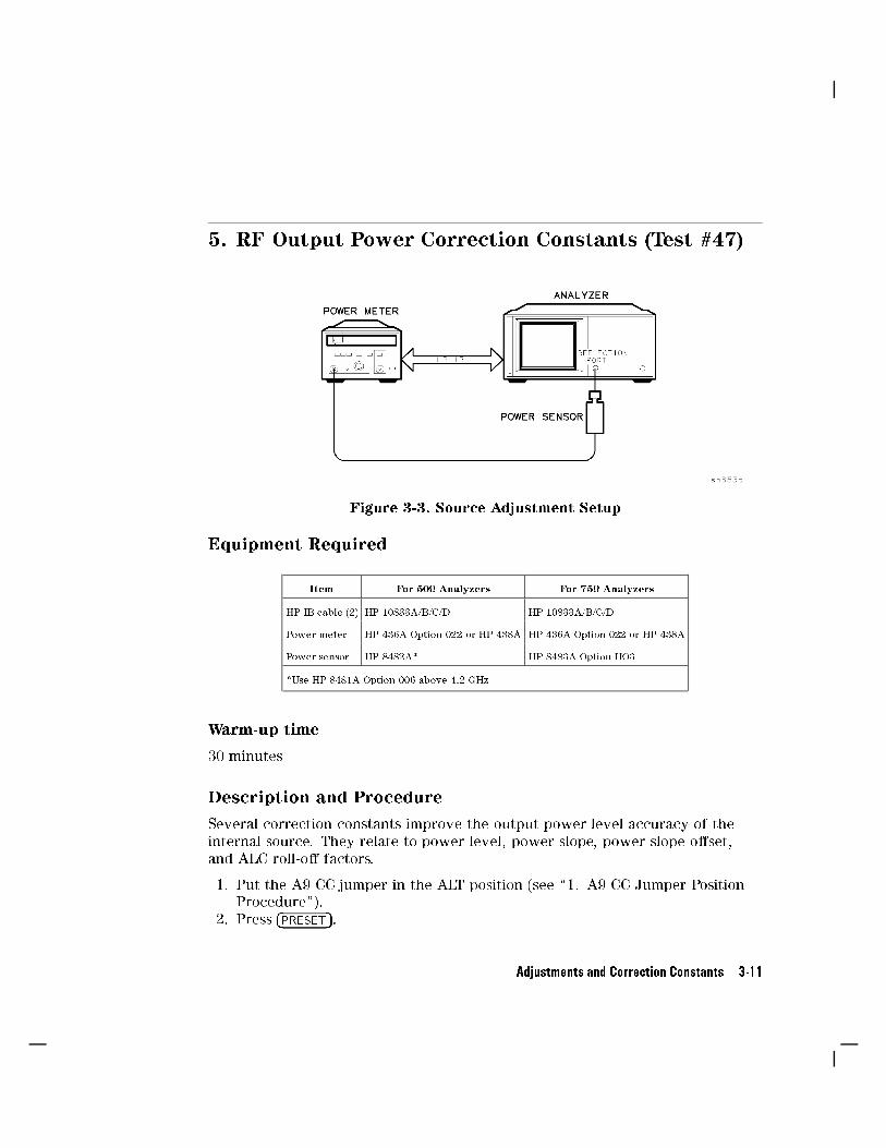
5. RF Output Power Correction Constants (Test #47)
Figure 3-3. Source Adjustment Setup
Equipment Required
Item For 50 Analyzers For 75 Analyzers
HP-IB cable (2) HP 10833A/B/C/D HP 10833A/B/C/D
Power meter HP 436A Option 022 or HP 438A HP 436A Option 022 or HP 438A
Power sensor HP 8482A* HP 8483A Option HO3
*Use HP 8481A Option 006 above 4.2 GHz
Warm-up time
30 minutes
Description and Procedure
Several correction constants improve the output power level accuracy of theinternal source. They relate to power level, power slope, power slope o�set,
and ALC roll-o� factors.
1. Put the A9 CC jumper in the ALT position (see \1. A9 CC Jumper PositionProcedure").
2. Press �PRESET�.
Adjustments and Correction Constants 3-11

3. Press �SYSTEM�NNNNNNNNNNNNNNNNNNNNNNNNNNNNNNNNNNNNNNSERVICE MENU
NNNNNNNNNNNNNNNNNTESTS �44� �x1�
NNNNNNNNNNNNNNNNNNNNNNNNNNNNNNNNNNNNNNEXECUTE TEST
NNNNNNNNNNNYES to write
default correction constants for rudimentary source power accuracy.4. Press �PRESET� �MEAS�
NNNNNNNNNNNNNNNNNNNNNNNNNNNNNNNNNNNINPUT PORTS
NNNNNR to measure input R.
5. Press �LOCAL�NNNNNNNNNNNNNNNNNNNNNNNNNNNNNNNNNNNNNNNNNNNNNNNNNNNNNSYSTEM CONTROLLER
NNNNNNNNNNNNNNNNNNNNNNNNNNNNNNNNNNNNNNNNNSET ADDRESSESNNNNNNNNNNNNNNNNNNNNNNNNNNNNNNNNNNNNNNNNNNNNNNNNNNNNNNNNNNNNNN
ADDRESS: P MTR/HPIB to see the address at which the analyzer
expects to �nd the power meter (the default address is 13). Refer to thepower meter manual as required to observe or change its address to 13.
6. PressNNNNNNNNNNNNNNNNNNNNNNNNNNNNNNNNNNNNNNNNNNNNNNNNNNNNNNNNNNNPOWER MTR: 438A/437 to toggle between 438A/437 and 436A to
match your power meter model number. When using the HP 438A, usechannel A.
Note If you are using an HP 438A power meter, connect the
HP 8482A power sensor to channel A, and the HP 8481A powersensor to channel B.
Power Sensor Calibration Factor Entry
7. Press �SYSTEM�NNNNNNNNNNNNNNNNNNNNNNNNNNNNNNNNNNNNNNSERVICE MENU
NNNNNNNNNNNNNNNNNNNNNNNNNNNNNNNNNNNNNNTEST OPTIONS
NNNNNNNNNNNNNNNNNNNNNNNNNNNNNNNNNNNNNNNNNNNNNNNNNNLOSS/SENSR LISTS
NNNNNNNNNNNNNNNNNNNNNNNNNNNNNNNNNNNNNNNNNNNNNNNNNNNNNNNNNNNCAL FACTOR SENSOR A to access the calibration factor menu.
Note In this menu, you can build a table of up to twelve points(twelve frequencies with their cal factors). Cal factor andfrequency values are listed on the back of the power sensor.
Input the cal factor frequency as GHz or MHz by pressing the appropriateentry key.Input cal factor percentages as whole numbers (for example, enter CALFACTOR 98% as 98).
The following terms are part of the sensor calibration menu:
NNNNNNNNNNNNNNNNNNNNNNNSEGMENT : press the softkey and use RPG or entry keys to select a point,
NNNNNNNNNNNNNNEDIT : press the softkey to change a previously entered value,
NNNNNNNNNNNNNNNNNNNNDELETE : press the softkey to delete a point from the table,
NNNNNNNNNNNADD : press the softkey to add a point to the table,
3-12 Adjustments and Correction Constants

NNNNNNNNNNNNNNNNNNNNNNNNNNNNNNNNCLEAR LIST : press the softkey to erase the entire table,
NNNNNNNNNNNNNNDONE : press the softkey when a table is complete and correct.
8. Press the appropriate softkeys to build a sensor calibration table.
Note The Sensor's reference calibration factor is the calibration factorfor 50 MHz.
9. Carefully zero and calibrate the power meter/sensor (refer to the powermeter/sensor manual as required).
Source Correction Routine
10. Press �SYSTEM�NNNNNNNNNNNNNNNNNNNNNNNNNNNNNNNNNNNNNNSERVICE MENU
NNNNNNNNNNNNNNNNNTESTS �47� �x1� to display Source Cor.
11. PressNNNNNNNNNNNNNNNNNNNNNNNNNNNNNNNNNNNNNNEXECUTE TEST and
NNNNNNNNNNNYES at the prompt to alter the correction
constants.
12. When prompted, connect the equipment as shown in Figure 3-3.13. Follow the instructions on the screen and press
NNNNNNNNNNNNNNNNNNNNNNNNNNCONTINUE . You can
reposition the marker as many times as required to achieve the attest line.
If there is no appreciable rollo�, position the marker at the highest
frequency. PressNNNNNNNNNNNNNNNNNNNNSELECT to select the marker position which most
e�ectively attens the trace.
DONE signals the successful conclusion of this routine. Refer to \15.
EEPROM Backup Disk Procedure" to store the new correction constants.Return the A9 CC jumper to the NRM position (see \1. A9 CC JumperPosition Procedure").FAIL is best handled by performing this procedure again.In case of continued failure, refer to the chapter titled \SourceTroubleshooting."
Adjustments and Correction Constants 3-13
6. Source Pretune Correction Constants (Test #48)
Equipment Required
No equipment is required to perform this adjustment.
Warm-up time
30 minutes
Description and Procedure
This adjustment generates two correction constants which pretune the YIGoscillators to insure proper phase lock.
1. Put the A9 CC jumper in the ALT position (see \1. A9 CC Jumper Position
Procedure").2. Press �PRESET�.3. Press �SYSTEM�
NNNNNNNNNNNNNNNNNNNNNNNNNNNNNNNNNNNNNNSERVICE MENU
NNNNNNNNNNNNNNNNNTESTS �48� �x1�.
4. When the analyzer displays:
Pretune Cor
pressNNNNNNNNNNNNNNNNNNNNNNNNNNNNNNNNNNNNNNEXECUTE TEST . Press
NNNNNNNNNNNYES at the query to alter the correction
constants and observe the display:Pretune Cor DONE displayed: the adjustment is complete and can be tested
by pressing �PRESET� and again observing the display:
Normal operation observed: the adjustment is complete. Refer to \15.
EEPROM Backup Disk Procedure" to store the new correction constants.Return the A9 CC jumper to the NRM position (see \1. A9 CC JumperPosition Procedure").Error messages observed: refer to the chapter titled \SourceTroubleshooting."Continued improper operation: refer to the chapter titled \SourceTroubleshooting."
3-14 Adjustments and Correction Constants

7. Display Intensity Adjustments (Test #49)
Equipment Required
Item Model Number
Photometer Tektronix J16
Photometer probe Tektronix J6503
Light occluder Tektronix 016-0305-00
Warm-up time
30 minutes
Description and Procedure
There are three display intensity adjustments:
1. background
2. maximum
3. operating default
Perform these adjustments when either the A19 GSP, A9 CPU, or A18 display
assemblies are replaced (as indicated in \Assembly Replacement and Post-Repair
Procedures").
Note This procedure should be performed with a photometer and onlyby quali�ed service personnel.
Background Adjustment
1. Put the A9 CC jumper in the ALT position (see \1. A9 CC Jumper Position
Procedure").2. In a dimly lit room (or with the analyzer's display shaded from bright
lights), press �PRESET�.
Adjustments and Correction Constants 3-15

3. Press �SYSTEM�NNNNNNNNNNNNNNNNNNNNNNNNNNNNNNNNNNNNNNSERVICE MENU
NNNNNNNNNNNNNNNNNTESTS �49� �x1�.
4. The analyzer should display:
Intensity Cor �ND�
Note The display could be so far out of adjustment that theannotation will be very di�cult to read.
5. PressNNNNNNNNNNNNNNNNNNNNNNNNNNNNNNNNNNNNNNEXECUTE TEST (top softkey) and
NNNNNNNNNNNYES (second from top softkey) at
the prompt to alter the correction constants. Alternating vertical bars ofthree di�erent intensities will be drawn on the display. Each bar has anumber written below it (either 0, 1, or 2).
6. Adjust the analyzer's RPG knob until the vertical bar labeled \1" is just
barely visible against the black border. Vertical bar \0" must not be visible.
Maximum Intensity Adjustment
This adjustment ensures that the light output at the 100% intensity level isequal to, or less than, 150 NITs. The level is set using a photometer to measure
the display's light output level.
Caution Operating the display at intensities higher than 150 NITs mayreduce the life of the display.
3-16 Adjustments and Correction Constants

Figure 3-4. Maximum Intensity Adjustment Set-up
7. Press the top softkey.
8. Set the photometer probe to NORMAL. Press �POWER� on the photometer to
switch it on and allow 30 minutes warm-up. Zero the photometer according
to the manufacturer's instructions. The analyzer display should have an all
white screen.
9. Center the photometer on the analyzer's display as shown in Figure 3-4.Adjust the analyzer's RPG knob to the maximum (clockwise) position. If
the photometer registers greater than 150 NITs, turn the RPG knob until areading of no more than 150 NITs registers on the photometer without the
bezel (90 NITS with the bezel). If the photometer registers a reading of lessthan 150 NITs and greater than 100 NITs, proceed to the next step. If thephotometer registers a reading of less than 100 NITs, the display is faulty.
Note The above intensity levels are read without a display bezelinstalled. The glass �lter transmits 60% of the display light,therefore 150 NITs would be 90 NITs with the bezel installed.
Adjustments and Correction Constants 3-17

Operating Default Intensity Adjustment
This adjustment sets the display's default intensity level. The analyzer normallypresets to the same intensity level that was last used. This level is stored involatile memory. If the memory is lost, the analyzer will use the default displayintensity to ensure that the display is visible and to eliminate concern that thedisplay may not be functioning.
10. Press the top softkey on the analyzer to bring up the next displayadjustment mode.
11. Center the photometer on the analyzer's display as shown in Figure 3-4.Adjust the analyzer's RPG knob until the photometer registers 100 NITs ofoutput light if the glass bezel assembly is not installed.
Adjust for 60 NITs if the glass bezel is installed.
12. Press the top softkey on the analyzer and observe the display:If DONE is displayed: the adjustment is complete. Refer to \15. EEPROM
Backup Disk Procedure" to store the new correction constants. Thiscompletes the series of three display intensity adjustments. Return the
A9 CC jumper to the NRM position (see \1. A9 CC Jumper Position
Procedure").If the analyzer continues to operate improperly: refer to \StartTroubleshooting Here" to isolate the problem.
3-18 Adjustments and Correction Constants

8. IF Ampli�er Correction Constants (Test #51)
Equipment Required
Item 50 Analyzers 75 Analyzers
RF cable HP PN 8120-4781 HP PN 8120-4781
Pad attenuator N/A HP 8491A Option 020
50/75 min loss pad (2) N/A HP 11852B
Warm-up time
30 minutes
Description and Procedure
Figure 3-5. IF Ampli�er Correction Constant Setup
These correction constants compensate for possible discontinuities of signalsgreater than �30 dBm.
Adjustments and Correction Constants 3-19
1. Put the A9 CC jumper in the ALT position (see \1. A9 CC Jumper PositionProcedure").
2. Press �PRESET�.3. Press �SYSTEM�
NNNNNNNNNNNNNNNNNNNNNNNNNNNNNNNNNNNNNNSERVICE MENU
NNNNNNNNNNNNNNNNNTESTS �51� �x1�.
4. PressNNNNNNNNNNNNNNNNNNNNNNNNNNNNNNNNNNNNNNEXECUTE TEST
5. When
IF Step Cor
appears on the display, pressNNNNNNNNNNNYES at the query to alter the correction
constants.6. At the prompt, remove any cable or device from the re ection port. PressNNNNNNNNNNNNNNNNNNNNNNNNNN
CONTINUE .
7. At the prompt, connect the attenuator and RF cable as shown in Figure 3-5.
PressNNNNNNNNNNNNNNNNNNNNNNNNNNCONTINUE .
8. If DONE is displayed: the adjustment is complete. Refer to \15. EEPROM
Backup Disk Procedure" to store the new correction constants. Return
the A9 CC jumper to the NRM position (see \1. A9 CC Jumper PositionProcedure").
9. If the procedure does not end with DONE, check the A9 CC jumper and the
setup and repeat. In case of di�culty, refer to the chapter titled \Digital
Control Troubleshooting."
3-20 Adjustments and Correction Constants

9. ADC O�set Correction Constants (Test #52)
Equipment
No equipment is required to perform this adjustment.
Warm-up time
30 minutes
Description and Procedure
These correction constants improve dynamic accuracy by shifting small signalsto the most linear part of the ADC quantizing curve.
1. Put the A9 CC jumper in the ALT position (see \1. A9 CC Jumper Position
Procedure").2. Press �PRESET�.3. Press �SYSTEM�
NNNNNNNNNNNNNNNNNNNNNNNNNNNNNNNNNNNNNNSERVICE MENU
NNNNNNNNNNNNNNNNNTESTS �52� �x1�. When the analyzer displays:
ADC Ofs Cor
pressNNNNNNNNNNNNNNNNNNNNNNNNNNNNNNNNNNNNNNEXECUTE TEST .
4. PressNNNNNNNNNNNYES at the query to alter the correction constants. Observe the
display:ADC Ofs Cor DONE displayed: the adjustment is complete. Refer to \15.
EEPROM Backup Disk Procedure" to store the new correction constants.
Return the A9 CC jumper to the NRM position (see \1. A9 CC JumperPosition Procedure").ADC Ofs Cor FAIL displayed: rerun the routine; in case of continued
improper operation, refer to the chapter titled \Digital ControlTroubleshooting."
Adjustments and Correction Constants 3-21
10. Frequency Response Correction Constants(Tests #53 and #57)
Equipment Required
Item 50 Analyzers 75 Analyzers
RF cable HP PN 8120-4781 HP PN 8120-2408
type-N calibration kit HP 85032B HP 85036B
Warm-up time
30 minutes
Description and Procedure
Perform \5. RF Output Power Correction Constants (Test #47)" before
continuing if you have replaced one or more of these assemblies:
A3 sourceA9 CPUA30 directional couplerAT1 attenuator
Note This procedure must be performed with the RF cable that willbe used with the analyzer. When the RF cable is replaced, this
procedure should be performed again to keep the correction
constants current.
1. Put the A9 CC jumper in the ALT position (see \1. A9 CC Jumper PositionProcedure").
2. Press �PRESET�.3. Press �SYSTEM�
NNNNNNNNNNNNNNNNNNNNNNNNNNNNNNNNNNNNNNSERVICE MENU
NNNNNNNNNNNNNNNNNTESTS �57� �x1�
NNNNNNNNNNNNNNNNNNNNNNNNNNNNNNNNNNNNNNEXECUTE TEST
NNNNNNNNNNNYES .
4. Press �SYSTEM�NNNNNNNNNNNNNNNNNNNNNNNNNNNNNNNNNNNNNNSERVICE MENU
NNNNNNNNNNNNNNNNNTESTS �53� �x1�.
5. When Freq Resp Cor -ND- appears, pressNNNNNNNNNNNNNNNNNNNNNNNNNNNNNNNNNNNNNNEXECUTE TEST
NNNNNNNNNNNYES . This allows
the correction constants to be altered.6. Connect a standard, as prompted on the display, then press the
corresponding softkey.
3-22 Adjustments and Correction Constants
Note For open and short standards, you must select an additionalsoftkey that indicates whether the test port is male or female.In this case, it is female (f).
7. PressNNNNNNNNNNNNNNDONE after the standard is measured.
8. Measure all three standard types (short, open, load).9. Press
NNNNNNNNNNNNNNDONE
NNNNNNNNNNNNNNNNNNNNNNNNNNNNNNNN1-PORT CAL to allow the analyzer to compute the calibration
coe�cients. This takes about 20 seconds.10. Connect the RF cable between the re ection and transmission test ports.11. Press
NNNNNNNNNNNNNNTHRU .
12. After the analyzer underlines THRU on the display, pressNNNNNNNNNNNNNNNNNNNNNNNNNNNNNNNNNNNNNNNNNNNNDONE: RESPONSE .
13. When the procedure is �nished, look at the display:If DONE is displayed, this procedure is complete. Store the new correction
constants to disk. Refer to \15. EEPROM Backup Disk Procedure."Return the A9 CC jumper to the NRM position (see \1. A9 CC JumperPosition Procedure").
If FAIL is displayed, refer to the chapter titled \Receiver
Troubleshooting."
Adjustments and Correction Constants 3-23

11. Cavity Oscillator Frequency Correction Constants(Test #54)
Equipment Required
Item 50 Analyzers 75 Analyzers
Low-pass �lter HP PN 9135-0198 HP PN 9135-0198
RF cable HP PN 8120-4781 HP PN 8120-4781
50 to 75 minimum loss pad (2) N/A HP 11852B
APC-3.5(f) to type-N(m) adapter 1250-1744 1250-1744
APC-3.5(m) to type-N(f) adapter 1250-1750 1250-1750
Warm-up time
30 minutes
Description and Procedure
Figure 3-6. Cavity Oscillator Frequency Correction Constant Setup
3-24 Adjustments and Correction Constants

The nominal frequency of the cavity oscillator is 2.982 GHz, but it varies withtemperature. This procedure determines the precise frequency of the cavityoscillator at a particular temperature by identifying a known spur.
Note With the �lter, the operator needs to distinguish between onlytwo spurs, each of which should be 10 dB to 20 dB (3 to 4divisions) above the trace noise.
Without the �lter, the target spur is one of four or �ve spurs,each of which may be 0.002 to 0.010 dB (invisible to 2 divisions)above or below the trace noise.
1. Put the A9 CC jumper in the ALT position (see \1. A9 CC Jumper Position
Procedure").2. Connect the equipment as shown in Figure 3-6 and switch the analyzer's
line power on.3. Press �PRESET�.4. Press �SYSTEM�
NNNNNNNNNNNNNNNNNNNNNNNNNNNNNNNNNNNNNNSERVICE MENU
NNNNNNNNNNNNNNNNNTESTS �54� �x1�.
5. When the analyzer displays:
Cav Osc Cor
pressNNNNNNNNNNNNNNNNNNNNNNNNNNNNNNNNNNNNNNEXECUTE TEST . Then press
NNNNNNNNNNNYES at the query to alter the correction
constants.
Note During this adjustment routine, you will see several softkeys:NNNNNNNNNNNNNNNNNNNNNNNNNNCONTINUE sweeps the current frequency span (may be
pressed repeatedly for additional looks at the currentfrequency span).NNNNNNNNNNNNNNNEXT sweeps the next frequency span (2 MHz higher).
NNNNNNNNNNNNNNNNNNNNSELECT enters the value of the marker (which should be on
the spur) and exits the routine.NNNNNNNNNNNNNNNNNABORT exits the routine.
6. PressNNNNNNNNNNNNNNNNNNNNNNNNNNCONTINUE to sweep the �rst frequency span three times. If there are
no spurs displayed, pressNNNNNNNNNNNNNNNEXT .
Adjustments and Correction Constants 3-25

Note Each new span overlaps the previous span by 3 MHz (thecenter frequency increases by 2 MHz; the span is 5 MHz). Thusanything visible on the right half of the display on one set ofsweeps will appear on the left half or center of the display.
7. PressNNNNNNNNNNNNNNNEXT repeatedly while watching the trace on each sweep and trying
to spot the target spur. With the �lter, the target spur will be one of twoobvious spurs (see Figure 3-7). Without the �lter (not recommended), it willbe one of four or �ve less distinct spurs as shown in Figure 3-9, Figure 3-10,and Figure 3-11.
When the center frequency increases to 2994.999 MHz and you have nottargeted the selected spur, Cav Osc Cor FAIL appears on the display.
8. If you are con�dent that you found the target spur, continue with step 9
(�lter procedure) or step 11 (�lterless procedure). Otherwise repeat steps 5through 8.
Spur Search Procedure with Filter
9. With the �lter, the target spur will appear to the right of a second spur,
similar to Figure 3-7. Rotate the RPG knob to position the marker on thespur.
3-26 Adjustments and Correction Constants

Figure 3-7. Typical Target Spur Using Filter
10. PressNNNNNNNNNNNNNNNNNNNNSELECT and observe the display:
DONE appears: the procedure has been performed successfully. Referto \15. EEPROM Backup Disk Procedure" to store the new correctionconstants.
If ND (not done) is displayed, repeat this procedure. Refer to \Source
Troubleshooting" if ND is still displayed.
Adjustments and Correction Constants 3-27

Spur Search Procedure without Filter
Figure 3-8. Cavity Oscillator Frequency Correction Alternative Setup
11. Connect the test equipment as shown in Figure 3-8.12. Without the �lter, the target spur will appear in a variety of disguises.
Often it will be di�cult to identify positively; occasionally it will be nearly
impossible to identify. PressNNNNNNNNNNNNNNNNNNNNNNNNNNCONTINUE as many times as necessary to
thoroughly inspect the current span. Without the �lter, the target spur
usually appears as one of a group of four evenly spaced spurs, as in
Figure 3-9. The target spur is the right-most spur (fourth from the left). Onany particular sweep, any or all of the spurs may be large, small, visible,
invisible, above or below the reference line.
3-28 Adjustments and Correction Constants
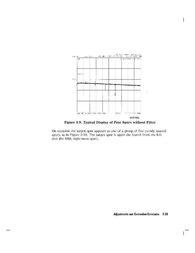
Figure 3-9. Typical Display of Four Spurs without Filter
On occasion the target spur appears as one of a group of �ve evenly spacedspurs, as in Figure 3-10. The target spur is again the fourth from the left
(not the �fth, right-most spur).
Adjustments and Correction Constants 3-29

Figure 3-10. Typical Display of Five Spurs without Filter
Figure 3-11 shows another variation of the basic four spur pattern: someup, some down and the target spur itself almost indistinguishable.
3-30 Adjustments and Correction Constants

Figure 3-11. Variation of Display of Four Spurs without Filter
13. Rotate the RPG knob to position the marker on the target spur. Then pressNNNNNNNNNNNNNNNNNNNNSELECT and observe the display:
DONE appears: the procedure has been performed successfully. Referto \15. EEPROM Backup Disk Procedure" to store the new correctionconstants. Return the A9 CC jumper to the NRM position (see \1. A9 CC
Jumper Position Procedure").
If ND (not done) is displayed, repeat this procedure. Refer to \SourceTroubleshooting" if ND is still displayed.
Adjustments and Correction Constants 3-31

12. Serial Number Correction Constant (Test #55)
Equipment
No equipment is required for this adjustment.
Warm-up time
5 minutes
Description and Procedure
This procedure customizes the replacement A9 CPU assembly by storing theanalyzer's unique serial number as a correction constant in EEPROM.
Caution Perform this procedure ONLY if the A9 CPU assembly has beenreplaced.
1. Put the A9 CC jumper in the ALT position (see \1. A9 CC Jumper Position
Procedure").
2. Note the ten-character serial number on the analyzer's rear panelidenti�cation label.
3. Press �PRESET�.
Caution Mistakes cannot be corrected after step 5 is performed.
4. Press �DISPLAY�NNNNNNNNNNNNNNMORE
NNNNNNNNNNNNNNNNNTITLE
NNNNNNNNNNNNNNNNNNNNNNNNNNNNNNNNNNNERASE TITLE to erase the HP logo. Rotate the
RPG knob to position the arrow below each character of the analyzer serial
number and pressNNNNNNNNNNNNNNNNNNNNNNNNNNNNNNNNNNNNNNNNNSELECT LETTER to enter each in turn. Enter a total of ten
characters: four digits, one letter, and �ve �nal digits.
PressNNNNNNNNNNNNNNNNNNNNNNNNNNNNNBACKSPACE if you made a mistake. Press
NNNNNNNNNNNNNNDONE when the title is
complete and correct.5. Press �SYSTEM�
NNNNNNNNNNNNNNNNNNNNNNNNNNNNNNNNNNNNNNSERVICE MENU
NNNNNNNNNNNNNNNNNTESTS �55� �x1�. When the display shows:
Serial Cor
pressNNNNNNNNNNNNNNNNNNNNNNNNNNNNNNNNNNNNNNEXECUTE TEST . Press
NNNNNNNNNNNYES at the query to alter the correction
constant.
3-32 Adjustments and Correction Constants

6. If this procedure did not end with DONE:The serial number entered did not conform to the required format, ora valid serial number was already stored.
In any case:Con�rm that the serial number is correct, andrepeat this procedure.
Contact HP if the procedure still does not end with DONE.7. To check the serial number recognized by the analyzer, press �PRESET�
�SYSTEM�NNNNNNNNNNNNNNNNNNNNNNNNNNNNNNNNNNNNNNSERVICE MENU
NNNNNNNNNNNNNNNNNNNNNNNNNNNNNNNNNNNNNNNNNNNNNNNNNNNNNFIRMWARE REVISION . The analyzer displays the
new serial number (SER. NO.). If not, repeat steps 3 through 6.8. Refer to \15. EEPROM Backup Disk Procedure" to store the new correction
constants. Return the A9 CC jumper to the NRM position (see \1. A9 CC
Jumper Position Procedure").
Adjustments and Correction Constants 3-33

13. Option Numbers Correction Constant (Test #56)
Equipment
No equipment is required for this adjustment.
Warm-up time
5 minutes
Figure 3-12. Location of Keyword Label
3-34 Adjustments and Correction Constants

Description and Procedure
Special information is stored in the A9 CPU assembly if an analyzer has any of(or any combination of) these options:
003 (3 GHz operation)004 (attenuator)006 (6 GHz operation)010 (time domain)
This procedure restores that information after an A9 CPU assembly has beenreplaced.
Perform this procedure only if:
the analyzer has one or more of the above options, and
the A9 CPU assembly has been replaced, and
the serial number correction constant procedure has been performed.
1. Put the A9 CC jumper in the ALT position (see \1. A9 CC Jumper PositionProcedure").
2. Note the keyword label on the display (see Figure 3-12). The label has onekeyword for each option installed in the analyzer. If the analyzer lacks a
label, call your local HP Sales and Service o�ce to obtain the keyword(s). Be
prepared to tell the service engineer the analyzer's full serial number and theoptions about to be installed on the analyzer.
3. Press �PRESET�.4. Press �DISPLAY�
NNNNNNNNNNNNNNMORE
NNNNNNNNNNNNNNNNNTITLE
NNNNNNNNNNNNNNNNNNNNNNNNNNNNNNNNNNNERASE TITLE . Rotate the RPG knob to
position the arrow below each character of the �rst keyword, and pressNNNNNNNNNNNNNNNNNNNNNNNNNNNNNNNNNNNNNNNNNSELECT LETTER to enter each in turn.
PressNNNNNNNNNNNNNNNNNNNNNNNNNNNNNBACKSPACE if you made a mistake. When you have �nished entering
the keyword, pressNNNNNNNNNNNNNNDONE .
Adjustments and Correction Constants 3-35

5. Press �SYSTEM�NNNNNNNNNNNNNNNNNNNNNNNNNNNNNNNNNNNNNNSERVICE MENU
NNNNNNNNNNNNNNNNNTESTS �56� �x1�. When the display shows:
Option Cor
pressNNNNNNNNNNNNNNNNNNNNNNNNNNNNNNNNNNNNNNEXECUTE TEST . Press
NNNNNNNNNNNYES at the query to alter the correction
constant and observe the analyzer's display:If DONE is displayed: the adjustment is complete. Continue with step 6.FAIL is displayed: check the keyword again to make sure it is correct,particularly if it contains the letters \I" or \O" or the numbers \1" or \0".Repeat the procedure beginning with step 2. If the procedure continues tofail, contact HP.
6. If the analyzer has more than one option, repeat steps 3, 4, and 5 to installthe remaining options. Refer to \15. EEPROM Backup Disk Procedure" tostore the new correction constants.
7. Return the A9 CC jumper to the NRM position (see \1. A9 CC JumperPosition Procedure").
Option 004 Installation
1. Press �SYSTEM�NNNNNNNNNNNNNNNNNNNNNNNNNNNNNNNNNNNNNNSERVICE MENU
NNNNNNNNNNNNNNNNNNNNNNNNNNNNNPEEK/POKE
NNNNNNNNNNNNNNNNNNNNNNNNNNNNNNNNNNNNNNNNNNNNNNNNNNNNNPEEK/POKE ADDRESS �2621814� �x1�NNNNNNNNNNNNNN
POKE ��1� �x1�.
2. Press �PRESET� �SYSTEM�NNNNNNNNNNNNNNNNNNNNNNNNNNNNNNNNNNNNNNSERVICE MENU
NNNNNNNNNNNNNNNNNNNNNNNNNNNNNNNNNNNNNNNNNNNNNNNNNNNNNFIRMWARE REVISION .
3. Verify that Option 004 is shown on the analyzer's display.
4. Refer to \15. EEPROM Backup Disk Procedure" to store the new correctionconstants.
5. Return the A9 CC jumper to the NRM position (see \1. A9 CC JumperPosition Procedure").
3-36 Adjustments and Correction Constants

14. Initialize EEPROMs (Test #58)
This service internal test performs the following functions:
destroys all correction constants and all un-protected optionsinitializes certain EEPROM address locations to zerosreplaces the display intensity correction constants with default values
Note This routine will not alter the serial number or Options 003, 006and 010 correction constants.
1. Press �PRESET� �SYSTEM�NNNNNNNNNNNNNNNNNNNNNNNNNNNNNNNNNNNNNNSERVICE MENU
NNNNNNNNNNNNNNNNNTESTS �58� �x1�
NNNNNNNNNNNNNNNNNNNNNNNNNNNNNNNNNNNNNNEXECUTE TEST
NNNNNNNNNNNYES .
2. To restore the analyzer's error correction constants:
If you have the correction constants backed up on a disk, refer to the\EEPROM Backup Disk Procedure."
If you don't have the correction constants backed up on a disk, run all theinternal service routines in the following order:
Source Default Correction Constants (Test #44)
Source Pretune Correction Constants (Test #45)
Analog Bus Correction Constants (Test #46)
RF Output Power Correction Constants (Test #47)Source Pretune Correction Constants (Test #48)
Display Intensity (Test #49)
IF Ampli�er Correction Constants (Test #51)
ADC O�set Correction Constants (Test #52)
Frequency Response Correction Constants (Test #57 then #53)Calibration Kit Default Correction Constants (Test #57)Cavity Oscillator Frequency Correction Constants (Test #54)
Adjustments and Correction Constants 3-37

15. EEPROM Backup Disk Procedure
Equipment Required
Item HP Model
CS80 disk drive HP 9122
HP-IB cable HP 10833A/B/C/D
3.5-inch disk blank disk or supplied EEPROM Calibration Data Disk
Warm-up time
None
Description and Procedure
Figure 3-13. EEPROM Backup Procedure Setup
A unique EEPROM Calibration Data Disk is shipped from the factory witheach analyzer. This disk is a record of the calibration constants (CCs) stored inEEPROM on the A9 CPU assembly. It allows you to replace the A9 CPU board
assembly without having to rerun all of the correction constant adjustment
procedures.
Take care of the supplied EEPROM Calibration Data Disk:If you don't have the original, make a backup disk and keep it current.
Store the correction constant data to the EEPROM Calibration Data Disk eachtime you perform one or more correction constant routines.
3-38 Adjustments and Correction Constants

Retrieve correction constant data from the EEPROM Calibration Data Disk ifyou need to replace the A9 CPU board assembly.
How to Make an EEPROM Backup Disk and Store CCs and Data
to It
1. Set the disk drive to HP-IB address 00. Insert a disk in drive 0.2. Connect the instruments as shown in Figure 3-13. Switch on the analyzer
�rst, followed by the disk drive.
3. Press �LOCAL�NNNNNNNNNNNNNNNNNNNNNNNNNNNNNNNNNNNNNNNNNNNNNNNNNNNNNSYSTEM CONTROLLER .
4. Press �SAVE/RECALL�NNNNNNNNNNNNNNNNNNNNNNNNNNNNNNNNNNNSELECT DISK
NNNNNNNNNNNNNNNNNNNNNNNNNNNNNNNNNNNNNNNNNNNNNNNNNNNNNNNNCONFIGURE EXT DISK . Set the disk
address, disk unit number, and volume number to 0.5. Press
NNNNNNNNNNNNNNNNNNNNRETURN
NNNNNNNNNNNNNNNNNNNNNNNNNNNNNNNNNNNNNNNNNEXTERNAL DISK :
If the NA does not toggle fromNNNNNNNNNNNNNNNNNNNNNNNNNNNNNNNNNNNNNNNNNNNNNNNINTERNAL MEMORY to
NNNNNNNNNNNNNNNNNNNNNNNNNNNNNNNNNNNNNNNNNEXTERNAL DISK :
Make sure the drive is powered up, its address correct, and that the
HP-IB cable is OK.Make sure the supplied disk or an initialized, non-write protected disk isin place:
If the disk is not initialized, press �SAVE/RECALL�NNNNNNNNNNNNNNNNNNNNNNNNNNNNNNNNNNNNNNNNNNNNFILE UTILITIES
NNNNNNNNNNNNNNNNNNNNNNNNNNNNNNNNNNNFORMAT DISK
NNNNNNNNNNNNNNNNNNNNNNNNNNNNNNNNNNNNNNNNNNNNNNNFORMAT EXT DISK
NNNNNNNNNNNYES .
6. Press �SYSTEM�NNNNNNNNNNNNNNNNNNNNNNNNNNNNNNNNNNNNNNSERVICE MENU
NNNNNNNNNNNNNNNNNNNNNNNNNNNNNNNNNNNNNNNNNSERVICE MODES
NNNNNNNNNNNNNNMORE
NNNNNNNNNNNNNNNNNNNNNNNNNNNNNNNNNNNNNNNNNSTORE EEPR ON
�SAVE/RECALL�NNNNNNNNNNNNNNNNNNNNNNNNNNNNNNNNSAVE STATE to store the EEPROM data with the instrument
state. This step stores the correction constants in a default �le named
\ISTATE0" on the oppy disk.
7. Press �SAVE/RECALL�NNNNNNNNNNNNNNNNNNNNNNNNNNNNNNNNNNNNNNNNNNNNFILE UTILITIES and use the RPG to highlight the �le
\ISTATE0."
8. PressNNNNNNNNNNNNNNNNNNNNNNNNNNNNNNNNNNNRENAME FILE
NNNNNNNNNNNNNNNNNNNNNNNNNNNNNNNNNNNERASE TITLE .
Then use the RPG and softkeys to title the �le N12345 (the �rst charactermust be a letter; 12345 represent the last �ve digits of the analyzer's serialnumber).
9. When �nished, pressNNNNNNNNNNNNNNDONE .
10. Label the disk with this information:the serial number of the analyzerthe words \EEPROM Backup Disk"today's date
Adjustments and Correction Constants 3-39
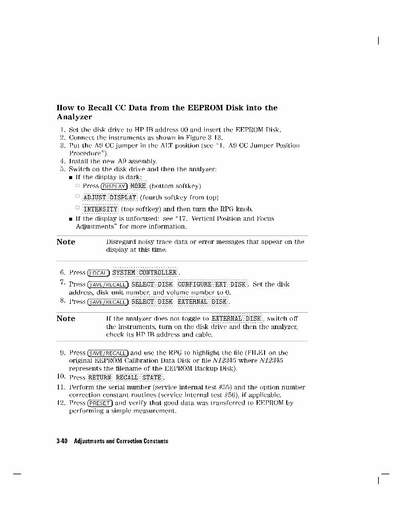
How to Recall CC Data from the EEPROM Disk into theAnalyzer
1. Set the disk drive to HP-IB address 00 and insert the EEPROM Disk.2. Connect the instruments as shown in Figure 3-13.3. Put the A9 CC jumper in the ALT position (see \1. A9 CC Jumper Position
Procedure").4. Install the new A9 assembly.5. Switch on the disk drive and then the analyzer:
If the display is dark:
Press �DISPLAY�NNNNNNNNNNNNNNMORE (bottom softkey)
NNNNNNNNNNNNNNNNNNNNNNNNNNNNNNNNNNNNNNNNNNNNADJUST DISPLAY (fourth softkey from top)NNNNNNNNNNNNNNNNNNNNNNNNNNNNNINTENSITY (top softkey) and then turn the RPG knob.
If the display is unfocused: see \17. Vertical Position and Focus
Adjustments" for more information.
Note Disregard noisy trace data or error messages that appear on thedisplay at this time.
6. Press �LOCAL�NNNNNNNNNNNNNNNNNNNNNNNNNNNNNNNNNNNNNNNNNNNNNNNNNNNNNSYSTEM CONTROLLER .
7. Press �SAVE/RECALL�NNNNNNNNNNNNNNNNNNNNNNNNNNNNNNNNNNNSELECT DISK
NNNNNNNNNNNNNNNNNNNNNNNNNNNNNNNNNNNNNNNNNNNNNNNNNNNNNNNNCONFIGURE EXT DISK . Set the disk
address, disk unit number, and volume number to 0.
8. Press �SAVE/RECALL�NNNNNNNNNNNNNNNNNNNNNNNNNNNNNNNNNNNSELECT DISK
NNNNNNNNNNNNNNNNNNNNNNNNNNNNNNNNNNNNNNNNNEXTERNAL DISK .
Note If the analyzer does not toggle toNNNNNNNNNNNNNNNNNNNNNNNNNNNNNNNNNNNNNNNNNEXTERNAL DISK , switch o�
the instruments, turn on the disk drive and then the analyzer,check its HP-IB address and cable.
9. Press �SAVE/RECALL� and use the RPG to highlight the �le (FILE1 on theoriginal EEPROM Calibration Data Disk or �le N12345 where N12345
represents the �lename of the EEPROM Backup Disk).10. Press
NNNNNNNNNNNNNNNNNNNNRETURN
NNNNNNNNNNNNNNNNNNNNNNNNNNNNNNNNNNNNNNRECALL STATE .
11. Perform the serial number (service internal test #55) and the option numbercorrection constant routines (service internal test #56), if applicable.
12. Press �PRESET� and verify that good data was transferred to EEPROM byperforming a simple measurement.
3-40 Adjustments and Correction Constants

13. Return the A9 CC jumper to the NRM position (see \1. A9 CC JumperPosition Procedure").In case of di�culty, refer to the chapter titled \Start TroubleshootingHere."
Adjustments and Correction Constants 3-41

16. Model Number Correction Constant(Option 075 Only)
Equipment
No equipment is required for this adjustment.
Warmup time
5 minutes
Description and Procedure
This procedure sets an EEPROM bit for HP 8752C analyzers with Option 075 sothat certain system default values will be correct after the A9 CPU assembly�rmware is replaced.
Firmware and A9 CPU assemblies are shipped with the bit set correctly forHP 8752C analyzers without Option 075.
Caution After installing new A9 CPU or new �rmware, but before
performing this procedure, perform \15. EEPROM Backup Disk
Procedure" found at the end of this chapter.
1. Put the A9 CC jumper in the ALT position (see \1. A9 CC Jumper Position
Procedure").2. Press �PRESET�.3. Press �SYSTEM�
NNNNNNNNNNNNNNNNNNNNNNNNNNNNNNNNNNNNNNSERVICE MENU
NNNNNNNNNNNNNNNNNNNNNNNNNNNNNPEEK/POKE
NNNNNNNNNNNNNNNNNNNNNNNNNNNNNNNNNNNNNNNNNNNNNNNNNNNNNPEEK/POKE ADDRESS �2621808� �x1�
NNNNNNNNNNNNNNPOKE �1� �x1�
NNNNNNNNNNNNNNNNNNNNNNNNNNNNNNNNNNNNNNNNNRESET MEMORY �PRESET�.
4. To verify that the procedure was successful, press �SYSTEM�NNNNNNNNNNNNNNNNNNNNNNNNNNNNNNNNNNNNNNSERVICE MENU
NNNNNNNNNNNNNNNNNNNNNNNNNNNNNNNNNNNNNNNNNNNNNNNNNNNNNFIRMWARE REVISION . Opt 075 should appear on the display. If Opt 075is not displayed, repeat the procedure. Contact the nearest HP sales and
service o�ce if the procedure was not successful.5. Return the A9 CC jumper to the NRM position (see \1. A9 CC Jumper
Position Procedure").
3-42 Adjustments and Correction Constants

17. Vertical Position and Focus Adjustments
Equipment
Narrow, non-conductive, athead screwdriver, 2-inches long
Warmup time
30 minutes
Description and Procedure
Only vertical position and focus, can be adjusted in the �eld (this includes both
customers and service centers). These adjustments are optional and should
rarely be required.
Caution Any other adjustments to the display will void the warranty.
Vertical Position Adjustment
1. To access vertical and focus adjustments controls, remove the side panel
nearest to the display.
Adjustments and Correction Constants 3-43

Figure 3-14. Vertical Position and Focus Adjustment Controls
2. Insert a narrow, non-conductive, at head screw driver (at least 2-inches
long) into the vertical position hole. See Figure 3-14.
3. Adjust the control until the softkey labels are aligned with the softkeys.
Focus Adjustment
4. Use the same screwdriver to adjust the focus until the display is the mostreadable.
3-44 Adjustments and Correction Constants

18. Display Degaussing (Demagnetizing)
Equipment
Any CRT demagnetizer or bulk tape eraser
Warm-up time
5 minutes
Description and Procedure
All color monitors are susceptible to external magnetic �elds. The usual
symptom is a discoloration or slight dimming, usually occurring near the top left
corner of the analyzer's display. In extreme cases, a total color shift may beobserved; for example, a trace that was red may shift to green.
Like most displays, the CRT can be sensitive to large magnetic �elds generated
from unshielded motors. In countries that use a 50 Hz line voltage frequency,
some 10 Hz jitter may be observed. If this problem is observed, remove thedevice causing the magnetic �eld.
Should the display become magnetized or if color purity is a problem, cyclethe power several times. Leave the analyzer o� for at least 30 seconds before
switching it on. This will activate the automatic degaussing circuitry in the
display. If this is insu�cient to achieve color purity, use a commercially
available demagnetizer (either a CRT demagnetizer or a bulk tape eraser).Follow the manufacturer's instructions keeping in mind the following:
Initially use the demagnetizer no closer than 4 inches (10 cm) from the face ofthe CRT.If needed, try again at a slightly closer distance until the CRT isdemagnetized.
Caution Applying a strong magnetic �eld to the CRT face canpermanently destroy it.
Adjustments and Correction Constants 3-45

19. Fractional-N Frequency Range Adjustment
Equipment Required
No equipment is required to perform this adjustment procedure.
Warm-up time
30 minutes
Description and Procedure
This adjustment centers the fractional-N VCO (voltage controlled oscillator) in its
tuning range to insure reliable operation of the analyzer.
1. Remove the analyzer right side panel.2. Press �PRESET�.3. Press �DISPLAY�
NNNNNNNNNNNNNNNNNNNNNNNNNNNNNNNNNNNNNNDUAL CHAN ON �MENU�
NNNNNNNNNNNNNNNNNNNNNNNNNNNNNNNNNNNNNNNNNNNNNNNNNNNUMBER of POINTS �11� �x1�NNNNNNNNNNNNNNNNNNNNNNNNNNNNNNNNNNNNNNNNNNNN
COUPLED CH OFF .
4. Press �START� �36� �M/u� �STOP� �60.75� �M/u� �MENU�NNNNNNNNNNNNNNNNNNNNNNNNNNNNNNNNSWEEP TIME �12.5� �k/m�
�SYSTEM�NNNNNNNNNNNNNNNNNNNNNNNNNNNNNNNNNNNNNNSERVICE MENU
NNNNNNNNNNNNNNNNNNNNNNNNNNNNNNNNNNNNNNNNNANALOG BUS ON �MEAS�
NNNNNNNNNNNNNNNNNNNNNNNNNNNNNNNNNNNNNNNNNNNNNNNNNNNNNNNNNNNANALOG IN Aux Input �29�
�x1� to observe the \FN VCO Tune" voltage.
Press �SCALE REF� �.6� �x1�NNNNNNNNNNNNNNNNNNNNNNNNNNNNNNNNNNNNNNNNNNNNNNNREFERENCE VALUE ��7� �x1� to set and scale
channel 1.5. Press �MKR� to set the marker to the far right of the graticule.
6. Press �CH 2� �MENU�NNNNNNNNNNNNNNNNNNNNNNNCW FREQ �31.0001� �M/u�
NNNNNNNNNNNNNNNNNNNNNNNNNNNNNNNNSWEEP TIME �12 .375� �k/m� �MEAS�NNNNNNNNNNNNNNNNNNNNNNNNNNNNNNNNNNNNNNNNNNNNNNNNNNNNNNNNNNN
ANALOG IN Aux Input �29� �x1� to observe the \FN VCO Tune" voltage. Press
�SCALE REF� �.2� �x1�NNNNNNNNNNNNNNNNNNNNNNNNNNNNNNNNNNNNNNNNNNNNNNNREFERENCE VALUE �6.77� �x1� �MKR� �6� �k/m� to set channel 2
and its marker.
3-46 Adjustments and Correction Constants

Figure 3-15. FN VCO TUNE Adjustment Location
7. Observe the analyzer display for the results of the adjustment.a. Refer to Figure 3-15. If the marker value is less than 7, the adjustment
procedure is complete.
Adjustments and Correction Constants 3-47
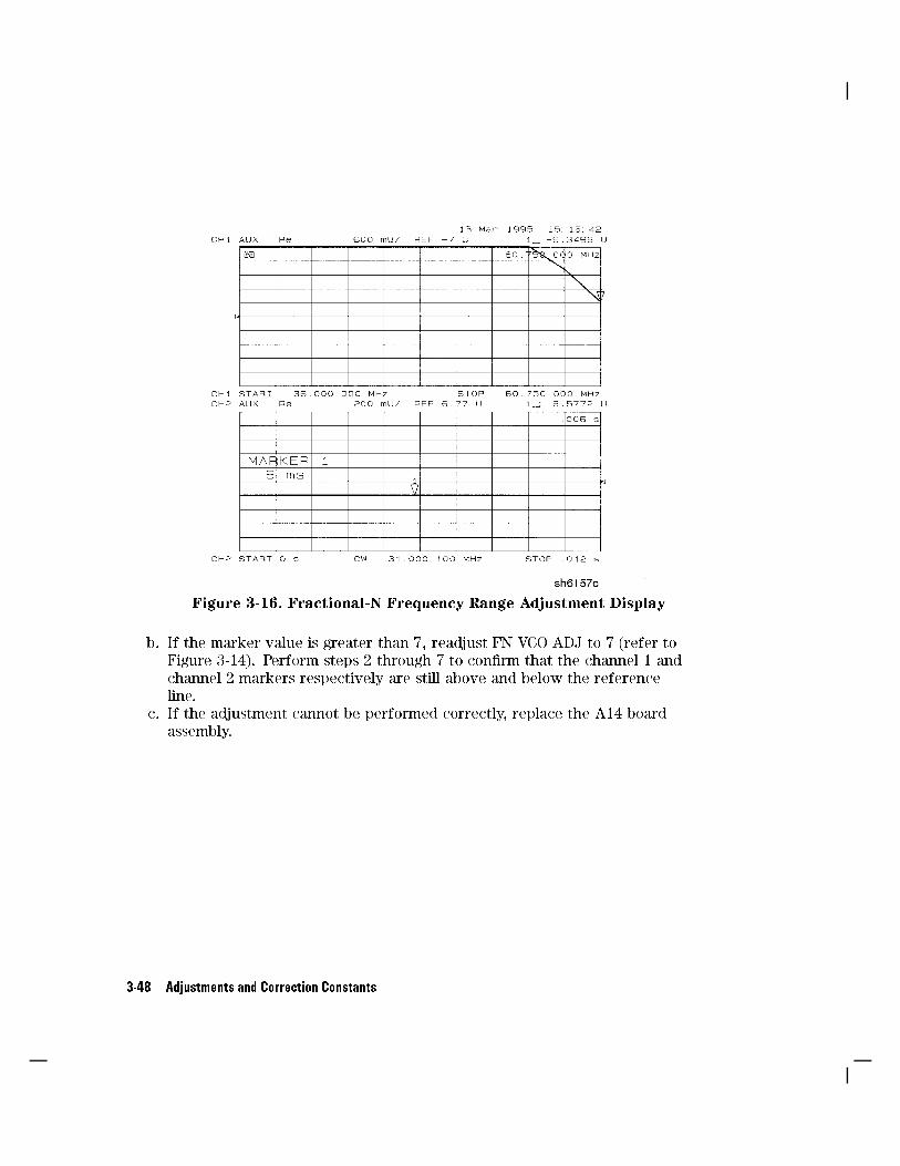
Figure 3-16. Fractional-N Frequency Range Adjustment Display
b. If the marker value is greater than 7, readjust FN VCO ADJ to 7 (refer to
Figure 3-14). Perform steps 2 through 7 to con�rm that the channel 1 and
channel 2 markers respectively are still above and below the reference
line.
c. If the adjustment cannot be performed correctly, replace the A14 board
assembly.
3-48 Adjustments and Correction Constants
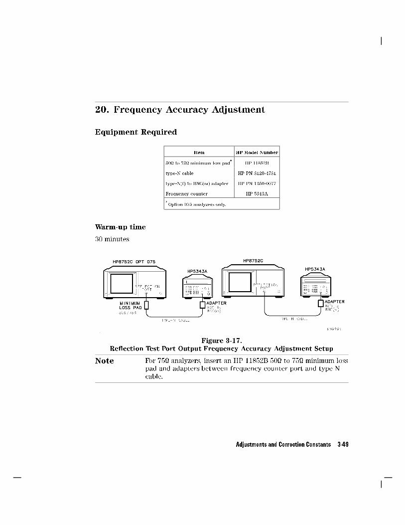
20. Frequency Accuracy Adjustment
Equipment Required
Item HP Model Number
50 to 75 minimum loss pad* HP 11852B
type-N cable HP PN 8120-4781
type-N(f) to BNC(m) adapter HP PN 1250-0077
Frequency counter HP 5343A
*Option 075 analyzers only.
Warm-up time
30 minutes
Figure 3-17.Re ection Test Port Output Frequency Accuracy Adjustment Setup
Note For 75 analyzers, insert an HP 11852B 50 to 75 minimum losspad and adapters between frequency counter port and type-Ncable.
Adjustments and Correction Constants 3-49

Description and Procedure
This adjustment sets the VCXO (voltage controlled crystal oscillator) frequencyto maintain the analyzer's frequency accuracy.
1. Remove the analyzer's top cover and connect the equipment as shown inFigure 3-17.
2. Press �PRESET�.3. Press �MENU�
NNNNNNNNNNNNNNNNNNNNNNNCW FREQ �50� �M/u� and note the frequency:
Frequency = 50 MHz �500 Hz: no adjustment is required.To adjust the frequency, locate the A12 assembly (red extractors) andadjust VCXO ADJ (see Figure 3-18) for a frequency counter reading of50 MHz �500 Hz.
4. If you are unable to adjust the frequency as speci�ed, replace the A12assembly.
Figure 3-18. VCXO ADJ Adjustment Location
3-50 Adjustments and Correction Constants

21. High/Low Band Transition Adjustment
Equipment Required
No equipment is required for this adjustment procedure.
Warm-up time
30 minutes
Description and Procedure
This adjustment centers the VCO (voltage controlled oscillator) of the A12
reference assembly for reliable high band and low band operation.
1. Remove the top cover (see \1. A9CC Jumper Position Procedure"). Remove
the PC board stabilizer and place the A12 assembly on an extender board.Use extension SMB cables as needed.
2. Press �PRESET�.3. Press �SYSTEM�
NNNNNNNNNNNNNNNNNNNNNNNNNNNNNNNNNNNNNNSERVICE MENU
NNNNNNNNNNNNNNNNNNNNNNNNNNNNNNNNNNNNNNNNNANALOG BUS ON �START� �11� �M/u� �STOP� �21�
�M/u� to observe part of both the low and high bands on the analog bus.
4. Press �MEAS�NNNNNNNNNNNNNNNNNNNNNNNNNNNNNNNNNNNNNNNNNNNNNNNNNNNNNNNNNNNANALOG IN Aux Input �22� �x1� �DISPLAY�
NNNNNNNNNNNNNNNNNNNNNNNNNNNNNDATA->MEM
NNNNNNNNNNNNNNNNNNNNNNNNNNDATA-MEM
to subtract the ground voltage from the next measurement.5. Press �MEAS�
NNNNNNNNNNNNNNNNNNNNNNNNNNNNNNNNNNNNNNNNNNNNNNNNNNNNNNNNNNNANALOG IN A12 Gnd 1 �23� �x1� �MKR� �11� �M/u�.
6. Press �MKR FCTN�NNNNNNNNNNNNNNNNNNNNNNNNNNNNNNNNNNNNNNNNNNNNNNNNNNNNNMARKER->REFERENCE �SCALE REF� �.1� �x1� and observe the
VCO tune voltage trace:
Left half of trace =0 �1000 mV and right half of trace =100 to 200 mV
higher (one to two divisions, see Figure 3-19): no adjustment necessary.
Adjustments and Correction Constants 3-51

Figure 3-19. High/Low Band Transition Adjustment Trace
To adjust: turn VCO TUNE (see Figure 3-20) to position the left half of the
trace to 0�125 mV. Then adjust HBLB to position the right half of the trace
125 to 175 mV (about 1 1/2 divisions) higher than the left half.
Figure 3-20. High/Low Band Adjustments Locations
3-52 Adjustments and Correction Constants

7. In some cases, the VCO TUNE adjustment may need to be performed �rst.If you are having trouble with the high low band adjustment, perform thefollowing procedure:a. Press:
�SYSTEM�NNNNNNNNNNNNNNNNNNNNNNNNNNNNNNNNNNNNNNSERVICE MENU
NNNNNNNNNNNNNNNNNNNNNNNNNNNNNNNNNNNNNNNNNANALOG BUS ON
�START� �10� �M/�� �STOP� �10� �M/��b. Press:
�MEAS�NNNNNNNNNNNNNNNNNNNNNNNNNNNNNNNNNNNNNNNNNNNNNNNNNNNNNNNNNNNANALOG IN Aux INPUT �22� �x1�
�DISPLAY�NNNNNNNNNNNNNNNNNNNNNNNNNNNNNNNNNNNNNNDATA->MEMORY
NNNNNNNNNNNNNNNNNNNNNNNNNNDATA-MEM
c. Press:
�MEAS�NNNNNNNNNNNNNNNNNNNNNNNNNNNNNNNNNNNNNNNNNNNNNNNNNNNNNNNNNNNANALOG IN Aux INPUT �23� �x1�
�FORMAT�NNNNNNNNNNNNNNMORE
NNNNNNNNNNNNNNREAL
d. Adjust C85 (VCO TUNE) to 0 units � 100 mU.
e. Press �SYSTEM�NNNNNNNNNNNNNNNNNNNNNNNNNNNNNNNNNNNNNNSERVICE MENU
NNNNNNNNNNNNNNNNNNNNNNNNNNNNNNNNNNNNNNNNNANALOG BUS ON �START� �11� �M/u� �STOP�
�21� �M/u� to observe part of both the low and high bands on the analog
bus.
f. Press �MEAS�NNNNNNNNNNNNNNNNNNNNNNNNNNNNNNNNNNNNNNNNNNNNNNNNNNNNNNNNNNNANALOG IN Aux Input �22� �x1� �DISPLAY�
NNNNNNNNNNNNNNNNNNNNNNNNNNNNNDATA->MEM
NNNNNNNNNNNNNNNNNNNNNNNNNNDATA-MEM to subtract the ground voltage from the next measurement.
g. Press �MEAS�NNNNNNNNNNNNNNNNNNNNNNNNNNNNNNNNNNNNNNNNNNNNNNNNNNNNNNNNNNNANALOG IN A12 Gnd 1 �23� �x1� �MKR� �11� �M/u�.
h. Press �MKR FCTN�NNNNNNNNNNNNNNNNNNNNNNNNNNNNNNNNNNNNNNNNNNNNNNNNNNNNNMARKER->REFERENCE �SCALE REF� �.1� �x1� and observe the
VCO tune voltage trace:Left half of trace =0 �1000 mV and right half of trace =100 to 200 mV
higher (one to two divisions, see Figure 3-19): no adjustment necessary.
If you still cannot perform the high/low band adjustment, refer to thechapter titled \Source Troubleshooting."
Adjustments and Correction Constants 3-53

22. Fractional-N Spur Avoidance and FM SidebandAdjustment
Equipment Required
Item HP Model Number
Spectrum Analyzer HP 8563E
RF Cable 50, type-N, 24-inch HP P/N 8120-4781
Cable, 50 Coax, BNC (m) to BNC (m) HP 10503A
Non-metallic Adjustment Tool HP P/N 8830-0024
Antistatic Wrist Strap HP P/N 9300-1367
Antistatic Wrist Strap Cord HP P/N 9300-0980
Static-control Table Mat and Earth Ground Wire HP P/N 9300-0797
50 to 75 Minimum Loss Pad* HP 11852B
*Option 075 analyzers only.
Warmup time
30 minutes
Description and Procedure
This adjustment minimizes the spurs caused by the API (analog phaseinterpolator, on the fractional-N assembly) circuits. It also improves thesideband characteristics.
1. Connect the equipment as shown in Figure 3-21.
2. Make sure the instruments are set to their default HP-IB addresses:HP 8752C = 16, Spectrum Analyzer = 18.
3-54 Adjustments and Correction Constants

Figure 3-21.Fractional-N Spur Avoidance and FM Sideband Adjustment Setup
3. Set the spectrum analyzer measurement parameters as follows:
Reference Level : : : : : : : : : : : : : : : : : : : : : : : : : : : : : : : : : : : : : : : : : : : : : : : : : : : : : : : 0 dBmResolution Bandwidth : : : : : : : : : : : : : : : : : : : : : : : : : : : : : : : : : : : : : : : : : : : : : : : : 100 Hz
Center Frequency: : : : : : : : : : : : : : : : : : : : : : : : : : : : : : : : : : : : : : : : : : :676.145105 MHz
Adjustments and Correction Constants 3-55

4. On the HP 8752C, press �PRESET� �CENTER� �676.045105� �M/��.
5. Refer to Figure 3-22. Adjust the 100 kHz (R77) for a null (minimumamplitude) on the spectrum analyzer. The minimum signal may, or may not,drop down into the noise oor.
Figure 3-22. Location of API and 100 kHz Adjustments
6. On the spectrum analyzer, set the center frequency for 676.048105 MHz.
7. On the HP 8752C, press �CENTER� �676.048105� �M/��.
8. Adjust the API1 (R35) for a null (minimum amplitude) on the spectrum
analyzer.
9. On the spectrum analyzer, set the center frequency for 676.007515 MHz.
10. On the HP 8752C, press �CENTER� �676.004515� �M/��.
11. Adjust the API2 (R43) for a null (minimum amplitude) on the spectrumanalyzer.
12. On the spectrum analyzer, set the center frequency for 676.003450 MHz.
13. On the HP 8752C, press �CENTER� �676.00045� �M/��.
14. Adjust the API3 (R45) for a null (minimum amplitude) on the spectrumanalyzer.
15. On the spectrum analyzer, set the center frequency for 676.003045 MHz.
3-56 Adjustments and Correction Constants
16. On the HP 8752C, press �CENTER� �676.000045� �M/��.
17. Adjust the API4 (R47) for a null (minimum amplitude) on the spectrumanalyzer.
In Case of Di�culty
18. If this adjustment cannot be performed satisfactorily, repeat the entireprocedure. If the adjustment is still unattainable, replace the A13 boardassembly.
Adjustments and Correction Constants 3-57

23. Source Spur Avoidance Tracking Adjustment
Equipment Required
Item HP Part Number
BNC-alligator clip adapter 8120-1292
BNC cable 8120-1840
Warm-up time
30 minutes
Description and Procedure
This adjustment optimizes tracking between the YO (YIG oscillator) and the
cavity oscillator when they are frequency o�set to avoid spurs. Optimizing
YO-cavity oscillator tracking minimizes uctuations in the phase-locked loop.
1. Mate a BNC-alligator clip to the BNC cable and connect the BNC end to AUX
INPUT on the rear panel. Connect the alligator-clip to A11TP10 (labeled �
ERR). Connect the shield clip to A11TP1 (GND), shown in Figure 3-23.
Figure 3-23. A11 Test Point and A3 CAV ADJ Locations
3-58 Adjustments and Correction Constants

2. Press �PRESET�.3. Press �CENTER� �400� �M/u� �SPAN� �50� �M/u� to generate a sweep from 375 MHz
to 425 MHz.4. Press �SYSTEM�
NNNNNNNNNNNNNNNNNNNNNNNNNNNNNNNNNNNNNNSERVICE MENU
NNNNNNNNNNNNNNNNNNNNNNNNNNNNNNNNNNNNNNNNNANALOG BUS ON �MEAS�NNNNNNNNNNNNNNNNNNNNNNNNNNNNNNNNNNNNNNNNNNNNNNNNNNNNNNNNNNN
ANALOG IN Aux Input �11� �x1� �SCALE REF� �10� �k/m� �MKR FCTN�NNNNNNNNNNNNNNNNNNNNNNNNNNNNNNNNNNNNNNNNNNNNNNNNNNNNNMARKER->REFERENCE to observe the phase-locked loop error voltage:
If spikes are not visible on the display (see Figure 3-24): no adjustment isnecessary.If spikes are excessive (see Figure 3-24): adjust the CAV ADJ potentiometer(see Figure 3-23) on the A3 source bias assembly to eliminate the spikes.
5. Refer to \Start Troubleshooting Here" if visible spikes persist.
Figure 3-24. Display of Acceptable Versus Excessive Spikes
Adjustments and Correction Constants 3-59


4
Start Troubleshooting Here
The information in this chapter helps you:
Identify the portion of the analyzer that is at fault.
Locate the speci�c troubleshooting procedures to identify the assembly orperipheral at fault.
To identify the portion of the analyzer at fault, follow these procedures:
Step 1. Initial Observations
Step 2. Con�dence Test
Step 3. HP-IB System Check
Step 4. Faulty Group Isolation
Start Troubleshooting Here 4-1

Assembly Replacement Sequence
The following steps show the sequence to replace an assembly in an HP 8752CNetwork Analyzer.
1. Identify the faulty group. Refer to the \Start Troubleshooting Here" chapter.Follow up with the appropriate troubleshooting chapter that identi�es thefaulty assembly.
2. Order a replacement assembly. Refer to the \Replaceable Parts" chapter.
3. Replace the faulty assembly and determine what adjustments are necessary.Refer to the \Assembly Replacement and Post-Repair Procedures" chapter.
4. Perform the necessary adjustments. Refer to the \Adjustments and
Correction Constants" chapter.
5. Perform the necessary performance tests. Refer to the \System Veri�cationand Performance Tests" chapter.
Having Your Analyzer Serviced
If your analyzer should fail any of the following checks, call the nearest HPsales or service o�ce for assistance. See the table titled \Hewlett-Packard Sales
and Service O�ces" in Chapter 15. If your analyzer needs to be returned to HP,
follow the steps below.
1. Choose the nearest HP service center. (Hewlett-Packard sales and service
o�ces are listed in the \Safety and Licensing" chapter.)
2. Include a detailed description of any failed test and any error message.
3. Ship the analyzer, using the original or comparable antistatic packagingmaterials.
4-2 Start Troubleshooting Here

Step 1. Initial Observations
Initiate the Analyzer Self-Test
1. Disconnect all devices and peripherals from the analyzer.
2. Switch on the analyzer and press �PRESET�.
3. Watch for the indications in the order shown in Figure 4-1 to determine if theanalyzer is operating correctly.
Figure 4-1. LED Power-up Sequence
If the Self-Test Failed
1. Check the AC line power to the analyzer.
2. Check the fuse (rating listed on rear panel, spare inside holder).
3. Check the line voltage setting (use small screwdriver to change).
4. If the problem persists, refer to \Step 4. Faulty Group Isolation".
Start Troubleshooting Here 4-3

Step 2. Con�dence Test
The con�dence test veri�es that the circuits in the analyzer are functioningproperly. However, it does not verify the accessories or the analyzerspeci�cations.
The resulting measurement must fall within a limit testing window to pass thetest. The window size is based on both source and receiver speci�cations. Thecharacteristics tested are combinations of: source match, re ection tracking,directivity, transmission tracking, noise oor, and crosstalk.
The con�dence test adds all the applicable error terms together. To separatethem out or to keep a record of them for maintenance, refer to the \ErrorTerms" chapter.
If you want to test the individual analyzer speci�cations then refer to the\Veri�cation and Performance Tests" chapter.
Procedure
1. Select the test data printing status.
If you do not want the test data to automatically print, continue withstep 2.
If you want to have the test data automatically print, press �PRESET�
�SYSTEM�NNNNNNNNNNNNNNNNNNNNNNNNNNNNNNNNNNNNNNSERVICE MENU
NNNNNNNNNNNNNNNNNNNNNNNNNNNNNNNNNNNNNNTEST OPTIONS
NNNNNNNNNNNNNNNNNNNNNNNNNNNNNRECORD ON .
Note When using an InkJet printer, the analyzer must be set to the
standard print mode through the �COPY� menu.
2. Press �SYSTEM�NNNNNNNNNNNNNNNNNNNNNNNNNNNNNNNNNNNNNNSERVICE MENU
NNNNNNNNNNNNNNNNNTESTS
NNNNNNNNNNNNNNNNNNNNNNNNNNNNNNNNNNNNNNNNNNNNEXTERNAL TESTS
NNNNNNNNNNNNNNNNNNNNNNNNNNNNNNNNNNNNNNEXECUTE TEST .
The analyzer should display a short description of the test and a reminder ofthe RECORD function.
3. PressNNNNNNNNNNNNNNNNNNNNNNNNNNCONTINUE to begin the test.
4. Disconnect all devices from the re ection test port, as prompted on theanalyzer display.
5. PressNNNNNNNNNNNNNNNNNNNNNNNNNNCONTINUE to run the \source match, tracking" test. There should be
a PASS/FAIL result displayed on the analyzer.
4-4 Start Troubleshooting Here

6. PressNNNNNNNNNNNNNNNNNNNNNNNNNNCONTINUE to run the \transmission crosstalk, noise oor" test. (With
the record function on, this test will automatically run). There should be aPASS/FAIL result displayed on the analyzer.
7. PressNNNNNNNNNNNNNNNNNNNNNNNNNNCONTINUE and then connect the RF cable supplied with the analyzer
between the re ection and transmission test ports.
8. PressNNNNNNNNNNNNNNNNNNNNNNNNNNCONTINUE to run the \transmission tracking, source/load match" test.
There should be a PASS/FAIL result displayed on the analyzer.
9. PressNNNNNNNNNNNNNNNNNNNNNNNNNNCONTINUE to run the \load match, directivity" test. (With the record
function on, this test will automatically run.) There should be a PASS/FAILresult displayed on the analyzer.
10. PressNNNNNNNNNNNNNNNNNNNNNNNNNNCONTINUE again.
The analyzer now displays the result of the con�dence test. If the testfailed:
It could be due to loose connections. Tighten all connections and repeat
the Con�dence Test.
It could be due to a bad frequency response correction. Run servicetest 53.
It could be due to a faulty RF cable. Run the cable con�dence test
(service test 22) or replace the cable. Run the veri�cation procedure(test 27) to identify which error term is causing the failure.
Cable Con�dence Test
This test provides an easy check of the RF performance of the transmissioncable supplied with the HP 8752C.
The test limits used are the sum of the HP 8752C speci�cations that apply, plusthe uncertainties in the measurement.
Procedure
1. Press �PRESET� �SYSTEM�NNNNNNNNNNNNNNNNNNNNNNNNNNNNNNNNNNNNNNSERVICE MENU
NNNNNNNNNNNNNNNNNTESTS
NNNNNNNNNNNNNNNNNNNNNNNNNNNNNNNNNNNNNNNNNNNNEXTERNAL TESTS �22� �x1�.
The analyzer should display:
TEST22 CABLE CONFID -ND-
Start Troubleshooting Here 4-5

2. PressNNNNNNNNNNNNNNNNNNNNNNNNNNNNNNNNNNNNNNEXECUTE TEST . The analyzer now displays a brief description of the
test and the test limits.
3. PressNNNNNNNNNNNNNNNNNNNNNNNNNNCONTINUE to begin the test. Connect an RF cable between the
re ection and the transmission test ports, as prompted on the analyzer.
4. PressNNNNNNNNNNNNNNNNNNNNNNNNNNCONTINUE and notice the PASS/FAIL result.
If the cable passes the test: pressNNNNNNNNNNNNNNNNNNNNNNNNNNCONTINUE again and move the cable
gently in all possible directions to see if it stays within the limits.
If the cable fails the test: replace the cable.
Refer to \Step 4. Faulty Group Isolation" in this chapter if the problem persists
and the analyzer does not use HP-IB.
4-6 Start Troubleshooting Here
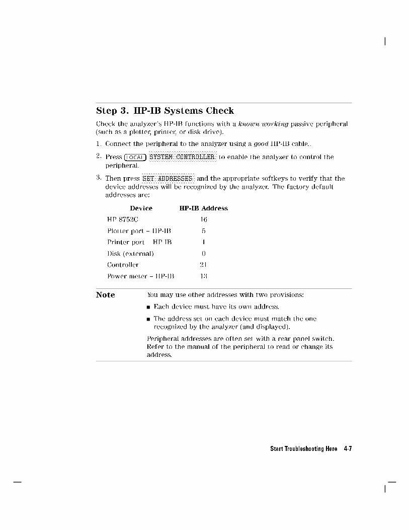
Step 3. HP-IB Systems Check
Check the analyzer's HP-IB functions with a known working passive peripheral(such as a plotter, printer, or disk drive).
1. Connect the peripheral to the analyzer using a good HP-IB cable..
2. Press �LOCAL�NNNNNNNNNNNNNNNNNNNNNNNNNNNNNNNNNNNNNNNNNNNNNNNNNNNNNSYSTEM CONTROLLER to enable the analyzer to control the
peripheral.
3. Then pressNNNNNNNNNNNNNNNNNNNNNNNNNNNNNNNNNNNNNNNNNSET ADDRESSES and the appropriate softkeys to verify that the
device addresses will be recognized by the analyzer. The factory defaultaddresses are:
Device HP-IB Address
HP 8752C 16
Plotter port { HP-IB 5
Printer port { HP-IB 1
Disk (external) 0
Controller 21
Power meter { HP-IB 13
Note You may use other addresses with two provisions:
Each device must have its own address.
The address set on each device must match the onerecognized by the analyzer (and displayed).
Peripheral addresses are often set with a rear panel switch.Refer to the manual of the peripheral to read or change itsaddress.
Start Troubleshooting Here 4-7

If Using a Plotter or Printer
1. Ensure that the plotter or printer is set up correctly:
power is on
pens and paper loaded
pinch wheels are down
some plotters need to have P1 and P2 positions set
2. Press �COPY� and thenNNNNNNNNNNNNNNPLOT or
NNNNNNNNNNNNNNNNNNNNNNNNNNNNNNNNNNNNNNNNNNNNNNNNNNPRINT MONOCHROME .
If the result is a copy of the analyzer display, the printing/plotting featuresare functional in the analyzer. Continue with \Troubleshooting Systems
with Multiple Peripherals," \Troubleshooting Systems with Controllers," or
the \Step 4. Faulty Group Isolation" section in this chapter.
If the result is not a copy of the analyzer display, suspect the HP-IBfunction of the analyzer: refer to the \Digital Control Troubleshooting"
chapter.
If Using an External Disk Drive
1. Select the external disk drive. Press �SAVE/RECALL�NNNNNNNNNNNNNNNNNNNNNNNNNNNNNNNNNNNSELECT DISKNNNNNNNNNNNNNNNNNNNNNNNNNNNNNNNNNNNNNNNNN
EXTERNAL DISK .
2. Verify that the address is set correctly. Press �LOCAL�NNNNNNNNNNNNNNNNNNNNNNNNNNNNNNNNNNNNNNNNNSET ADDRESSES
NNNNNNNNNNNNNNNNNNNNNNNNNNNNNNNNNNNNNNADDRESS:DISK .
3. Ensure that the disk drive is set up correctly:
power is on
an initialized disk in the correct drive
correct disk unit number and volume number (press �LOCAL� to access thesoftkeys that display the numbers; default is 0 for both)
with hard disk (Winchester) drives, make sure the con�guration switch is
properly set (see drive manual)
4-8 Start Troubleshooting Here

4. Press �START� �1� �M/�� �SAVE/RECALL�NNNNNNNNNNNNNNNNNNNNNNNNNNNNNNNNSAVE STATE . Then press �PRESET�
�SAVE/RECALL�NNNNNNNNNNNNNNNNNNNNNNNNNNNNNNNNNNNNNNRECALL STATE .
If the resultant trace starts at 1 MHz, HP-IB is functional in the analyzer.Continue with \Troubleshooting Systems with Multiple Peripherals,"\Troubleshooting Systems with Controllers," or the \Step 4. Faulty GroupIsolation" section in this chapter.
If the resultant trace does not start at 1 MHz, suspect the HP-IB functionof the analyzer: refer to the \Digital Control Troubleshooting" chapter.
Troubleshooting Systems with Multiple Peripherals
Connect any other system peripherals (but not a controller) to the analyzerone at a time and check their functionality. Any problems observed are in the
peripherals, cables, or are address problems (see above).
Troubleshooting Systems with Controllers
Passing the preceding checks indicates that the analyzer's peripheral functions
are normal. Therefore, if the analyzer has not been operating properly with an
external controller, suspect the controller. Check the following:
Compatibility of controller, must be HP 9000 series 200/300. (Refer to the\Service Equipment and Analyzer Options" chapter.)
HP-IB interface hardware is installed. (Refer to the manual, Installing and
Maintaining HP Basic/WS 6.2, that comes with your HP Basic software.)
Select code is correct. (Refer to the manual, Installing and MaintainingHP Basic/WS 6.2, that comes with your HP Basic software.)
I/O and HP-IB binaries are loaded. (Refer to the manual, Installing andMaintaining HP Basic/WS 6.2, that comes with your HP Basic software.)
HP-IB cables. (See \HP-IB Requirements" in the HP 8752C Network Analyzer
User's Guide.)
Programming syntax is correct. (Refer to the HP 8752C Network Analyzer
Programmer's Guide.)
If the analyzer appears to be operating unexpectedly but has not completelyfailed, go to \Step 4. Faulty Group Isolation."
Start Troubleshooting Here 4-9

Step 4. Faulty Group Isolation
Use the following procedures only if you have read the previous sections inthis chapter and you think the problem is in the analyzer. These are simpleprocedures to verify the four functional groups in sequence, and determinewhich group is faulty.
The four functional groups are:
power supplies
digital control
source
receiver
Descriptions of these groups are provided in the \Theory of Operation" chapter.
The checks in the following pages must be performed in the order presented.If one of the procedures fails, it is an indication that the problem is in the
functional group checked. Go to the troubleshooting information for the
indicated group, to isolate the problem to the defective assembly.
Figure 4-2 illustrates the troubleshooting organization.
Figure 4-2. Troubleshooting Organization
4-10 Start Troubleshooting Here

Power Supply Check
Check the Rear Panel LEDs
Switch on the analyzer. Notice the condition of the two LEDs on the A15preregulator at rear of the analyzer (see Figure 4-3).
The upper (red) LED should be o�.
The lower (green) LED should be on.
Figure 4-3. A15 Preregulator LEDs
Check the A8 Post Regulator LEDs
Remove the analyzer's top cover. Inspect the green LEDs along the top edge ofthe A8 post regulator assembly.
All green LEDs should be on.
The fan should be audible.
In case of di�culty, refer to the \Power Supply Troubleshooting" chapter.
Start Troubleshooting Here 4-11

Digital Control Check
Observe the Power Up Sequence
Switch the analyzer power o�, then on. The following should take place withina few seconds:
On the front panel observe the following:
1. All six amber LEDs illuminate.
2. The amber LEDs go o� after a few seconds, except the CH 1 LED. (SeeFigure 4-4).
The display should come up bright and focused.
Figure 4-4. Front Panel Power-up Sequence
4-12 Start Troubleshooting Here

Verify Internal Tests Passed
1. Press �PRESET� �SYSTEM�NNNNNNNNNNNNNNNNNNNNNNNNNNNNNNNNNNNNNNSERVICE MENU
NNNNNNNNNNNNNNNNNTESTS
NNNNNNNNNNNNNNNNNNNNNNNNNNNNNNNNNNNNNNNNNNNNINTERNAL TESTS
NNNNNNNNNNNNNNNNNNNNNNNNNNNNNNNNNNNNNNEXECUTE TEST . The display should indicate:
TEST0 ALL INT PASS
If your display shows the above message, go to step 2. Otherwise, continuewith this step.
If phase lock error messages are present, this test may stop without passingor failing. In this case, continue with the next procedure to check thesource.
If you have unexpected results, or if the analyzer indicates a speci�c test
failure, that internal test (and possibly others) have failed; the analyzer
reports the �rst failure detected. Refer to the \Service Key Menus and
Error Messages" chapter for internal test information; then refer to the\Digital Control Troubleshooting" chapter.
If the analyzer indicates failure but does not identify the test, press �*�to search for the failed test. (For a description of the failed test refer to
the \Service Key Menus" chapter.) Then refer to the \Digital Control
Troubleshooting" chapter. Likewise, if the response to front panel or HP-IBcommands is unexpected, troubleshoot the digital control group.
2. To perform the Analog Bus test, pressNNNNNNNNNNNNNNNNNNNNRETURN �19� ��1�
NNNNNNNNNNNNNNNNNNNNNNNNNNNNNNNNNNNNNNEXECUTE TEST .
If this test fails, refer to the \Digital Control Troubleshooting" chapter.
If this test passes, continue with the next procedure to check the source.
Source Check
1. Check the display for any of the following phase lock error messages:
NO IF FOUND: CHECK R INPUT LEVEL
NO PHASE LOCK: CHECK R INPUT LEVEL
PHASE LOCK LOST
PHASE LOCK CAL FAILED
If any of these error messages appear, refer to the \Source Troubleshooting"chapter. Otherwise, continue with the next step.
Start Troubleshooting Here 4-13

2. Connect the equipment as shown in Figure 4-5.
Item 50 Ohm NAs 75 Ohm NAs
Power meter HP 436A, 437B, or 438A
Power sensor HP 8482A HP 8483A Option H03*
* special option power sensor
Figure 4-5. Equipment Setup for Source Power Check
3. Switch on the instruments. Zero and calibrate the power meter.
4. On the analyzer, press �PRESET� Stimulus �MENU�NNNNNNNNNNNNNNNNNPOWER ��20� �x1� �MENU�NNNNNNNNNNNNNNNNNNNNNNN
CW FREQ �300� �K/m�. The power meter should read approximately �20 dBm
(�85 dBm for Option 004).
5. Press �16� �M/�� to change the CW frequency to 16 MHz. The power metershould read approximately �20 dBm throughout the analyzer's frequencyrange. Repeat checking the frequency at 1 GHz intervals up to the maximumfrequency of the analyzer.
6. PressNNNNNNNNNNNNNNNNNPOWER �5� �x1� to increase the output power to 5 dBm (+10 dBm for
Option 004).
7. Step through the frequencies as above: the power meter should readapproximately 5 dBm at all frequencies (+10 dBm with Option 004).
If any incorrect power levels are measured, refer to the \SourceTroubleshooting" chapter. Otherwise, continue with \Receiver Check."
4-14 Start Troubleshooting Here

Receiver Check
1. Connect an RF cable directly between the re ection and transmission ports.
2. On the analyzer, press �PRESET� �MEAS�NNNNNNNNNNNNNNNNNNNNNNNNNNNNNNNNNNNNNNTRANSMISSION �SCALE REF� �.5� �x1�.
3. Notice the condition of the trace: it should resemble Figure 4-6
If the trace shows unexpected results, refer to the \Receiver Troubleshooting"chapter.
Figure 4-6. Typical Measurement Trace
Accessories Check
If the analyzer has passed all of the above checks but is still making incorrectmeasurements, an accessory could be faulty: RF cables, interconnect cables, andcalibration kit devices can all induce system problems.
Recon�gure the system to its normal state and recon�rm the problem. If theproblem persists, refer to the \Accessories Troubleshooting" chapter.
Start Troubleshooting Here 4-15

4-16 Start Troubleshooting Here

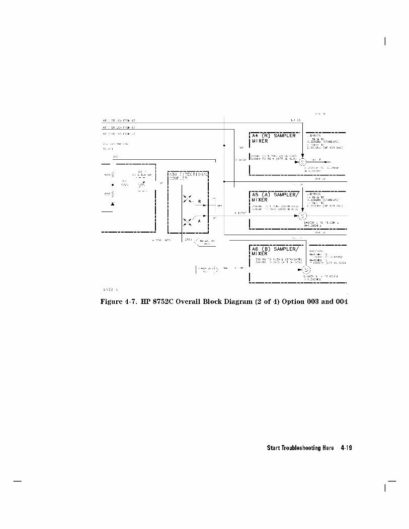
Figure 4-7. HP 8752C Overall Block Diagram (2 of 4) Option 003 and 004
Start Troubleshooting Here 4-19
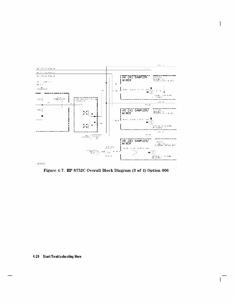
Figure 4-7. HP 8752C Overall Block Diagram (3 of 4) Option 006
4-20 Start Troubleshooting Here

Figure 4-7. HP 8752C Overall Block Diagram (4 of 4) Option 004 and 006
Start Troubleshooting Here 4-21


5
Power Supply Troubleshooting
Use this procedure only if you have read the \Start Troubleshooting Here"chapter. Follow the procedures in the order given, unless:
an error message appears on the display, refer to \Error Messages" near theend of this chapter.
the fan is not working, refer to \Fan Troubleshooting" in this chapter.
The power supply group assemblies consist of the following:
A8 post regulator
A15 preregulator
All assemblies, however, are related to the power supply group because power is
supplied to each assembly.
Power Supply Troubleshooting 5-1

Assembly Replacement Sequence
The following steps show the sequence to replace an assembly in an HP 8752CNetwork Analyzer.
1. Identify the faulty group. Refer to the \Start Troubleshooting Here" chapter.Follow up with the appropriate troubleshooting chapter that identi�es thefaulty assembly.
2. Order a replacement assembly. Refer to the \Replaceable Parts" chapter.
3. Replace the faulty assembly and determine what adjustments are necessary.Refer to the \Assembly Replacement and Post-Repair Procedures" chapter.
4. Perform the necessary adjustments. Refer to the \Adjustments and
Correction Constants" chapter.
5. Perform the necessary performance tests. Refer to the \System Veri�cationand Performance Tests" chapter.
5-2 Power Supply Troubleshooting
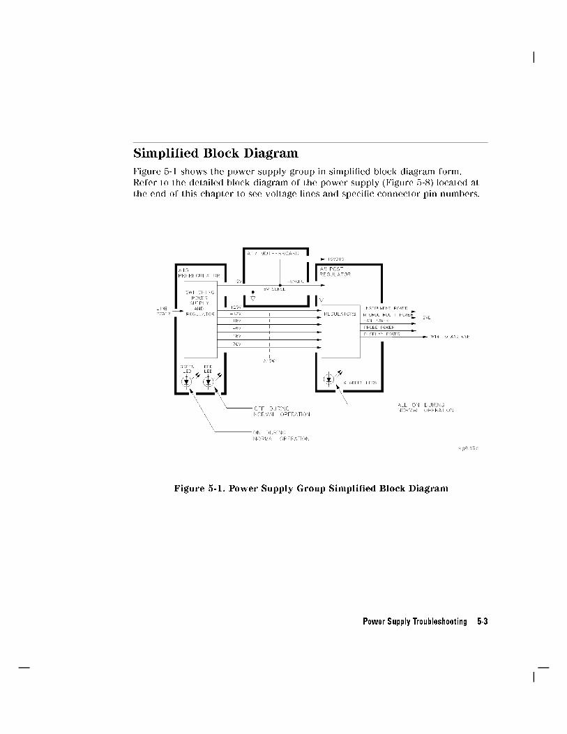
Simpli�ed Block Diagram
Figure 5-1 shows the power supply group in simpli�ed block diagram form.Refer to the detailed block diagram of the power supply (Figure 5-8) located atthe end of this chapter to see voltage lines and speci�c connector pin numbers.
Figure 5-1. Power Supply Group Simpli�ed Block Diagram
Power Supply Troubleshooting 5-3

Start Here
Check the Green LED and Red LED on A15
Switch on the analyzer and look at the rear panel of the analyzer. Check thetwo power supply diagnostic LEDs on the A15 preregulator casting by lookingthrough the holes located to the left of the line voltage selector switch (seeFigure 5-2).
During normal operation, the bottom (green) LED is on and the top (red) LED is
o�. If these LEDs are normal, then A15 is 95% veri�ed. Continue with \Check
the Green LEDs on A8".
If the green LED is not on steadily, refer to \If the Green LED on A15 is not
On Steadily" in this procedure.
If the red LED is on or ashing, refer to \If the Red LED On A15 is On" in
this procedure.
Figure 5-2. Location of A15 Diagnostic LEDs
5-4 Power Supply Troubleshooting

Check the Green LEDs on A8
1. Remove the top cover of the analyzer and locate the A8 post regulator. Usethe location diagram under the top cover if necessary.
2. Check to see if the green LEDs on the top edge of A8 are all on. Thereare nine green LEDs (one is not visible without removing the PC boardstabilizer).
If all of the green LEDs on the top edge of A8 are on, there is a 95%con�dence level that the power supply is veri�ed. To con�rm the last 5%uncertainty of the power supply, refer to \Measure the Post RegulatorVoltages" (next).
If any LED on the A8 post regulator is o� or ashing, refer to \If theGreen LEDs On A8 are not All On" in this chapter.
Measure the Post Regulator Voltages
Measure the DC voltages on the test points of A8 with a voltmeter. Refer to
Figure 5-3 for test point locations and Table 5-1 for supply voltages and limits.
Figure 5-3. A8 Post Regulator Test Point Locations
Power Supply Troubleshooting 5-5

Table 5-1. A8 Post Regulator Test Point Voltages
TP Supply Range
1 +65V +64.6 to +65.4
2 AGND n/a
3 +5 VD +4.9 to +5.3
4 SDIS n/a
5 �15V �14.4 to �15.6
6 �12.6 VPP (probe power) �12.1 to �12.8
7 +15V +14.5 to +15.5
8 +5 VU +5.05 to +5.35
9 �5.2 V �5.0 to �5.4
10 +22V +21.3 to +22.7
11 +6V +5.8 to +6.2
5-6 Power Supply Troubleshooting

If the Green LED on A15 is not On Steadily
If the green LED is not on steadily, the line voltage is missing or is not enoughto power the analyzer.
Check the Line Voltage, Selector Switch, and Fuse
1. Check the main power line cord, line fuse, line selector switch setting, andactual line voltage to see that they are all correct. Figure 5-4 shows how toremove the line fuse, using a small at-bladed screwdriver to pry out the fuseholder. Figure 5-2 shows the location of the line voltage selector switch.
2. Use a small at-bladed screwdriver to select the correct switch position.
If the A15 green LED is still not on steadily, replace A15.
Figure 5-4. Removing the Line Fuse
Power Supply Troubleshooting 5-7

If the Red LED On A15 is On
If the red LED is on or ashing, the power supply is shutting down. Use thefollowing procedures to determine which assembly is causing the problem.
Check the A8 Post Regulator
1. Switch o� the analyzer.
2. Disconnect the cable A15W1 from the A8 post regulator (see Figure 5-5).
3. Switch on the analyzer and observe the red LED on A15.
If the red LED goes out, the problem is probably the A8 post regulator.
Continue with \Verify the A15 Preregulator" to �rst verify that the inputs
to A8 are correct.
If the red LED is still on, the problem is probably the A15 preregulator, or
one of the assemblies obtaining power from it. Continue with \Check for aFaulty Assembly."
5-8 Power Supply Troubleshooting

Figure 5-5. Power Supply Cable Locations
Verify the A15 Preregulator
Verify that the A15 preregulator is supplying the correct voltages to the A8 postregulator. Use a voltmeter with a small probe to measure the output voltages ofA15W1's plug. Refer to Table 5-2 and Figure 5-6.
If the voltages are not within tolerance, replace A15.
If the voltages are within tolerance, A15 is veri�ed. Continue with \Check fora Faulty Assembly."
Power Supply Troubleshooting 5-9

Table 5-2. Output Voltages
Pin A15W1P1 (Disconnected)
Voltages
A8J2 (Connected) Voltages A15 Preregulator Mnemonic
1,2 +125 to +100 +68 to +72 +70V
3,4 +22.4 to +33.6 +17.0 to +18.4 +18V
5,6 �22.4 to �33.6 �17.0 to �18.4 �18V
7 N/C N/C N/C
8 +9.4 to +14 +7.4 to +8.0 +8 V
9,10 �9.4 to �14 �6.7 to �7.3 �8 V
11 +32 to +48 +24.6 to +26.6 +25V
12 N/C N/C N/C
NOTE: The +5VD supply must be loaded by one or more assemblies at all times, or the other voltages will not
be correct. It connects to motherboard connector A17J3 Pin 4.
5-10 Power Supply Troubleshooting

Figure 5-6. A15W1 Plug Detail
Check for a Faulty Assembly
This procedure checks for a faulty assembly that might be shutting down theA15 preregulator via one of the following lines (also refer to Figure 5-1):
the A15W1 cable connected to the A8 post regulator
the +5VCPU line through the motherboard
the +5VDIG line through the motherboard
Power Supply Troubleshooting 5-11

Do the following:
1. Switch o� the analyzer.
2. Ensure that A15W1 is reconnected to A8 (refer to Figure 5-5).
3. Remove or disconnect the assemblies listed in Table 5-3 one at a time and inthe order shown. The assemblies are sorted from most to least accessible.Table 5-3 also lists any associated assemblies that receive power from
the assembly that is being removed. After each assembly is removed or
disconnected, switch on the analyzer and observe the red LED on A15.
Note Always switch o� the analyzer before removing ordisconnecting assemblies.
When extensive disassembly is required, refer the \AssemblyReplacement and Post-Repair Procedures" chapter.
Refer to the \Replaceable Parts" chapter to identify speci�c
cables and assemblies that are not shown in this chapter.
If the red LED goes out, the particular assembly removed (or one receivingpower from it) is faulty.
If the red LED is still on after you have checked all of the assemblies listed inTable 5-3, continue with \Check the Operating Temperature."
Table 5-3. Recommended Order for Removal/Disconnection
Assembly
To Remove
Removal or
Disconnection Method
Other Assemblies that Receive
Power from the Removed Assembly
1. A19 Graphics Processor Disconnect W14 A18
Display
2. A14 Frac N Digital Remove from Card Cage None
3. A9 CPU Remove from Card Cage None
4. A16 Rear Panel Interface Disconnect A16W1 None
5. A2 Front Panel Interface Disconnect W17 A1 Front Panel
Keyboard
5-12 Power Supply Troubleshooting

Check the Operating Temperature
The temperature sensing circuitry inside the A15 preregulator may be shuttingdown the supply. Make sure the temperature of the open air operatingenvironment does not exceed 55 �C (131 �F), and that the analyzer fan isoperating.
If the fan does not seem to be operating correctly, refer to \FanTroubleshooting" at the end of this procedure.
If there does not appear to be a temperature problem, it is likely that A15 isfaulty.
Inspect the Motherboard
If the red LED is still on after replacement or repair of A15, switch o� theanalyzer and inspect the motherboard for solder bridges, and other noticeable
defects. Use an ohmmeter to check for shorts. The +5VD, +5VCPU, or
+5VDSENSE lines may be bad. Refer to the block diagram (Figure 5-8) at theend of this chapter and troubleshoot these suspected power supply lines on theA17 motherboard.
Power Supply Troubleshooting 5-13

If the Green LEDs On A8 are not All On
The green LEDs along the top edge of the A8 post regulator are normally on.
Flashing LEDs on A8 indicate that the shutdown circuitry on the A8 postregulator is protecting power supplies from overcurrent conditions byrepeatedly shutting them down. This may be caused by supply loading on A8 oron any other assembly in the analyzer.
Remove A8, Maintain A15W1 Cable Connection
1. Switch o� the analyzer.
2. Remove A8 from its motherboard connector, but keep the A15W1 cable
connected to A8.
3. Remove the display power cable W14 (see Figure 5-5).
4. Short A8TP2 (AGND) (see Figure 5-3) to chassis ground with a clip lead.
5. Switch on the analyzer and observe the green LEDs on A8.
If any green LEDs other than +5VD are still o� or ashing, continue with\Check the A8 Fuses and Voltages."
If all LEDs are now on steadily except for the +5VD LED, the A15
preregulator and A8 post regulator are working properly and the troubleis excessive loading somewhere after the motherboard connections at A8.Continue with \Remove the Assemblies."
Check the A8 Fuses and Voltages
Check the fuses along the top edge of A8. If any A8 fuse has burned out,replace it. If it burns out again when power is applied to the analyzer, A8 orA15 is faulty. Determine which assembly has failed as follows.
1. Remove the A15W1 cable at A8 (see Figure 5-5).
2. Measure the voltages at A15W1P1 (see Figure 5-6) with a voltmeter that hasa small probe.
3. Compare the measured voltages with those in Table 5-2.
If the voltages are within tolerance, replace A8.
If the voltages are not within tolerance, replace A15.
5-14 Power Supply Troubleshooting

If the green LEDs are now on, the A15 preregulator and A8 post regulator areworking properly and the trouble is excessive loading somewhere after themotherboard connections at A8. Continue with \Remove the Assemblies."
Remove the Assemblies
1. Switch o� the analyzer.
2. Install A8. Remove the jumper from A8TP2 (AGND) to chassis ground.
3. Remove or disconnect all the assemblies listed below (see Figure 5-5).Always switch o� the analyzer before removing or disconnecting anassembly.
A9 CPUA10 digital IFA11 phase lockA12 referenceA13 fractional-N analogA14 fractional-N digitalA19 graphics processor (disconnect W14, A18W1, and W20)
4. Switch on the analyzer and observe the green LEDs on A8.
If any of the green LEDs are o� or ashing, it is not likely that any of theassemblies listed above is causing the problem. Continue with, \Brie yDisable the Shutdown Circuitry."
If all green LEDs are now on, one or more of the above assemblies may
be faulty. Continue with next step.
5. Switch o� the analyzer.
6. Reconnect W14 and W20 to A19.
7. Switch on the analyzer and observe the LEDs.
If the LEDs are o� or blinking, replace the A19 assembly.If the LEDs are still on, continue with next step.
8. Switch o� the analyzer.
9. Reconnect A18W1 to the A19 assembly.
10. Switch on the analyzer and observe the LEDs.
If the LEDs are o�, replace the A18 display.
If the LEDs are still on, continue with the next step.
Power Supply Troubleshooting 5-15

11. Switch o� the analyzer.
12. Reinstall each assembly one at a time. Switch on the analyzer after eachassembly is installed. The assembly that causes the green LEDs to go o� or ash could be faulty.
Note It is possible, however, that this condition is caused by theA8 post regulator not supplying enough current. To checkthis, reinstall the assemblies in a di�erent order to change theloading. If the same assembly appears to be faulty, replace thatassembly. If a di�erent assembly appears faulty, A8 is most
likely faulty (unless both of the other assemblies are faulty).
Brie y Disable the Shutdown Circuitry
In this step, you shutdown the protective circuitry for a short time, and the
supplies are forced on (including shorted supplies) with a 100% duty cycle.
Caution Damage to components or to circuit traces may occur if A8TP4(SDIS) is shorted to chassis ground for more than a few seconds.
1. Switch o� the analyzer.
2. Connect A8TP4 (SDIS) to chassis ground with a jumper wire.
3. Switch on the analyzer and notice the LEDs that are o�. Immediately
remove the jumper wire.
4. Refer to the block diagram (Figure 5-8) at the end of this chapter and do thefollowing:
a. Notice any additional signals that may connect to any A8 test point thatshowed a fault in the previous step.
b. Cross reference all assemblies that use the power supplies whose A8 LEDswent out when A8TP4 (SDIS) was connected to chassis ground.
5-16 Power Supply Troubleshooting

c. Make a list of these assemblies.
d. Delete the following assemblies from your list as they have already beenveri�ed earlier in this section.
A9 CPUA10 digital IFA11 phase lockA12 referenceA13 fractional-N analogA14 fractional-N digitalA18 displayA19 graphics processor
5. Switch o� the analyzer.
6. Of those assemblies that are left on the list, remove or disconnect themfrom the analyzer one at a time. Table 5-4 shows the best order in which
to remove them. Table 5-4 also lists any associated assemblies that recieve
power by the assembly that is being removed. After each assembly is
removed or disconnected switch on the analyzer and observe the LEDs.
Note Always switch o� the analyzer before removing ordisconnecting assemblies.
When extensive disassembly is required, refer to the\Assembly Replacement and Post-Repair Procedures" chapter.
Refer to the \Replaceable Parts" chapter to identify speci�c
cables and assemblies that are not shown in this chapter.
If all the LEDs light, the assembly removed (or one receiving power from it) isfaulty.
If the LEDs are still not on steadily, continue with \Inspect the Motherboard."
Power Supply Troubleshooting 5-17

Table 5-4. Recommended Order for Removal/Disconnection
Assembly
To Remove
Removal or
Disconnection Method
Other Assemblies that Receive
Power from the Removed Assembly
1. A3 Source Remove from Card Cage None
2. A7 Pulse Generator Remove from Card Cage None
3. A4 R Sampler Remove from Card Cage None
4. A5 A Sampler Remove from Card Cage None
5. A6 B Sampler Remove from Card Cage None
6. A2 Front Panel Interface Disconnect W17 A1 Front Panel
Keyboard
7. A16 Rear Panel Interface Disconnect A16W1 None
Inspect the Motherboard
Inspect the A17 motherboard for solder bridges and shorted traces. In
particular, inspect the traces that carry the supplies whose LEDs faulted when
A8TP4 (SDIS) was grounded earlier.
5-18 Power Supply Troubleshooting

Error Messages
Three error messages are associated with the power supplies functional group.They are shown here.
POWER SUPPLY SHUT DOWN!
One or more supplies on the A8 post regulator assembly is shut down due toone of the following conditions: overcurrent, overvoltage, or undervoltage.Refer to \If the Red LED On A15 is On" earlier in this procedure.
POWER SUPPLY HOT!
The temperature sensors on the A8 post regulator assembly detect anovertemperature condition. The regulated power supplies on A8 have beenshut down.
Check the temperature of the operating environment; it should not be greaterthan +55 �C (131 �F). The fan should be operating and there should be atleast 15 cm (6 in) spacing behind and all around the analyzer to allow forproper ventilation.
PROBE POWER SHUT DOWN!
The front panel RF probe biasing supplies are shut down due to excessivelydrawb current. These supplies are +15VPP and �12.6VPP, both supplied by
the A8 post regulator. +15VPP is derived from the +15V supply. �12.6VPP is
derived from the �12.6V supply.
Refer to Figure 5-7 and carefully measure the power supply voltages at thefront panel RF probe connectors.
Power Supply Troubleshooting 5-19

Figure 5-7. Front Panel Probe Power Connector Voltages
If the correct voltages are present, troubleshoot the probe.
If the voltages are not present, check the +15V and �12.6V green LEDs on
A8.
If the LEDs are on, there is an open between the A8 assembly and thefront panel probe power connectors. Put A8 onto an extender board and
measure the voltages at the following pins:
A8P2 pins 6 and 36 �12.6 volts
A8P2 pins 4 and 34 +15 volts
If the LEDs are o�, continue with \Check the Fuses and Isolate A8."
5-20 Power Supply Troubleshooting

Check the Fuses and Isolate A8
1. Check the fuses associated with each of these supplies near the A8 testpoints. If these fuses keep burning out, a short exists.
2. Try isolating A8 by removing it from the motherboard connector, but keepingthe cable A15W1 connected to A8J2.
3. Connect a jumper wire from A8TP2 to chassis ground.
If either the +15V or �12.6V fuse blows, or the associated green LEDs donot light, replace A8.
If the +15V and �12.6V green LEDs light, troubleshoot for a shortbetween the motherboard connector pins XA8P2 pins 6 and 36 (�12.6V)and the front panel probe power connectors. Also check between
motherboard connector pins XA8P2 pins 4 and 34 (+15V) and the frontpanel probe power connectors.
Power Supply Troubleshooting 5-21
Fan Troubleshooting
Fan Speeds
The fan speed varies depending upon temperature. It is normal for the fan tobe at high speed when the analyzer is just switched on, and then change to lowspeed when the analyzer is cooled.
Check the Fan Voltages
1. If the fan is dead, refer to the A8 post regulator block diagram (Figure 5-8)at the end of this chapter. The fan is driven by the +18V and �18V suppliescoming from the A15 preregulator. Neither of these supplies is fused.
The �18V supply is regulated on A8 in the fan drive block, and remains
constant at approximately �14 volts. It connects to the A17 motherboard via
pin 32 of the A8P1 connector.
The +18V supply is regulated on A8 but changes the voltage to the fan,depending on air ow and temperature information. Its voltage rangesfrom approximately �1.0 volts to +14.7 volts, and connects to the A17
motherboard via pin 31 of the A8P1 connector.
2. Measure the voltages of these supplies while using an extender board to
allow access to the PC board connector, A8P1.
Short A8TP3 to Ground
1. If there is no voltage at A8P1 pins 31 and 32, switch o� the analyzer.Remove A8 from its motherboard connector (or extender board) but keep thecable A15W1 connected to A8 (see Figure 5-5).
2. Connect a jumper wire between A8TP3 and chassis ground.
3. Switch on the analyzer and observe the green LEDs.
If all the green LEDs on the top edge of A8 light (except +5VD), replacethe fan.
If other green LEDs on A8 do not light, refer to \If the Green LEDs On A8are not All On" earlier in this procedure.
5-22 Power Supply Troubleshooting

Intermittent Problems
PRESET states that appear spontaneously (without pressing �PRESET�) typicallysignal a power supply or A9 CPU problem. Since the A9 CPU assembly isthe easiest to substitute, do so. If the problem ceases, replace the A9. If theproblem continues, replace the A15 preregulator assembly.
Power Supply Troubleshooting 5-23

5-24 Power Supply Troubleshooting
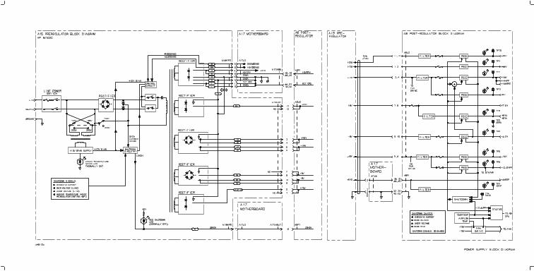

6
Digital Control Troubleshooting
Use this procedure only if you have read the \Start Troubleshooting Here"chapter. Follow the procedures in the order given, unless instructed otherwise.If you suspect an HP-IB interface problem, refer to \HP-IB Failures" at the endof this chapter.
The digital control group assemblies consist of the following:
A1 front panel keyboard
A2 front panel interface
A9 CPU
A10 digital IF
A16 rear panel
A18 display
A19 GSP
Digital Control Troubleshooting 6-1

Assembly Replacement Sequence
The following steps show the sequence to replace an assembly in an HP 8752CNetwork Analyzer.
1. Identify the faulty group. Refer to the \Start Troubleshooting Here" chapter.Follow up with the appropriate troubleshooting chapter that identi�es thefaulty assembly.
2. Order a replacement assembly. Refer to the \Replaceable Parts" chapter.
3. Replace the faulty assembly and determine what adjustments are necessary.Refer to the \Assembly Replacement and Post-Repair Procedures" chapter.
4. Perform the necessary adjustments. Refer to the \Adjustments and
Correction Constants" chapter.
5. Perform the necessary performance tests. Refer to the \System Veri�cationand Performance Tests" chapter.
6-2 Digital Control Troubleshooting

Digital Control Group Block Diagram
Figure 6-1. Digital Control Group Block Diagram
Digital Control Troubleshooting 6-3

Check A9 CPU Operation
A9 CC Jumper Positions
The A9 CC jumper must be in the \NRM" (normal) position for these procedures.This is the position for normal operating conditions. To move the jumper to the\NRM" position, do the following:
1. Unplug the analyzer.
2. Remove the top cover.
3. Remove the A9 CPU board.
4. Move the jumper to the NRM position. (Refer to Figure 6-2.)
5. Replace the A9 CPU board, top cover, and power cord.
Figure 6-2. Jumper Positions on the A9 CPU
6-4 Digital Control Troubleshooting

Checking A9 CPU Red LED Patterns
The A9 CPU has four red LEDs that can be viewed by removing the top cover.(Refer to \Major Assemblies" in Chapter 13 to locate the A9 CPU and Figure 6-3to identify the LEDs.)
1. Cycle the power
Cycle the power on the analyzer and observe the four red LEDs. All fourLEDs should be on after power up.
If the four LEDs did not illuminate, replace the A9 CPU after verifying thepower supply.
2. Hold in the preset key
Press and hold down the �PRESET� key while observing the four LEDs on A9.
The far left LED should be o�. (See Figure 6-3.)
Figure 6-3. Location of Four LEDs on A9 CPU
Digital Control Troubleshooting 6-5

3. Release the preset key
Release the �PRESET� key and watch for the rapid sequence shown below.Notice that the far left LED always remains on. (The �lled circles representilluminated LEDs.)
� � � � �PRESET� still held down
� � � � �PRESET� released { Pattern 1
� � � � Pattern 2
� � � � Pattern 3
� � � � Pattern 4
� � � � Pattern 5 { two left LEDs icker
� � � � Pattern 6
� � � � Pattern 7 { two left LEDs icker
4. Observe and evaluate results
If the above sequence is observed, and the far right LED remained on, goto \Check A19 GSP and A18 Display Operation."
If the right LED does not remain on, replace the A9 CPU assembly andrepeat the three LED pattern checks.
If the LEDs are held in any one of the patterns shown in Table 6-1, and
have the corresponding error message, replace the A9 �rmware ICs.
(Firmware ICs are not separately replaceable. Replacement kits are listedin the \Replaceable Parts" chapter.)
Table 6-1. LED Code and Pattern Versus Test Failed
LED Code Sum Message Displayed Faulty Component
RUN 1 2 4
� � � � ROM 1L FAIL U24
� � � � ROM 2L FAIL U25
� � � � ROM 1M FAIL U4
� � � � ROM 2M FAIL U5
6-6 Digital Control Troubleshooting

Check A19 GSP and A18 Display Operation
Cycle Power and Look at the Display
Switch the analyzer o�, and then on. The display should be bright and focusedwith the annotation legible and intelligible.
If the display is acceptable, go to \A1/A2 Front Panel Troubleshooting."
If the display is unacceptable, continue with the next step.
Perform Display Intensity and Focus Adjustments
Refer to the \Adjustments and Correction Constants" chapter, and perform the
\Display Intensity Adjustments." If this does not resolve the problem, refer to\A19 GSP and A18 Display Troubleshooting," located later in this chapter.
A1/A2 Front Panel Troubleshooting
Check Front Panel LEDs After Preset
1. Press �PRESET� on the analyzer.
2. Observe that all front panel LEDs turn on and, within �ve seconds afterreleasing �PRESET�, all but the CH1 LED turns o�. Refer to Figure 6-4.
If all the front panel LEDs either stay on or o�, there is a control problembetween A9 and A1/A2. See \Inspect Cables," located later in this chapter.
If, at the end of the turn on sequence, the channel 1 LED is not on and all
HP-IB status LEDs are not o�, continue with\Identify the Stuck Key."
Digital Control Troubleshooting 6-7

Figure 6-4. Preset Sequence
Identify the Stuck Key
Match the LED pattern with the patterns in Table 6-2. The LED pattern
identi�es the stuck key. Free the stuck key or replace the front panel part
causing the problem.
6-8 Digital Control Troubleshooting

Table 6-2. Front Panel Key Codes
Decimal
Number
LED Pattern Key Front Panel Block
CH1 CH2 R L T S
0 �CAL� Response
1 � �3� Entry
2 � �k/m� Entry
3 � � �DISPLAY� Response
4 � �AVG� Response
5 � � �2� Entry
6 � � �1� Entry
7 � � �???????????????????softkey 3 Softkey
8 �???????????????????softkey 5 Softkey
9 � � �9� Entry
10 � � �G/n� Entry
11 � � � �CH 1� Active Channel
12 � � �CH 2� Active Channel
13 � � � �8� Entry
14 � � � �7� Entry
15 � � � �???????????????????softkey 1 Softkey
16 � �STOP� Stimulus
17 � � �SAVE/RECALL� Instrument State
18 � � �SEQ� Instrument State
19 � � � �MENU� Stimulus
20 � � �START� Stimulus
21 � � � �COPY� Instrument State
22 � � � �SYSTEM� Instrument State
23 � � � �???????????????????softkey 6 Softkey
24 � � �SCALE REF� Response
25 � � � �6� Entry
Digital Control Troubleshooting 6-9
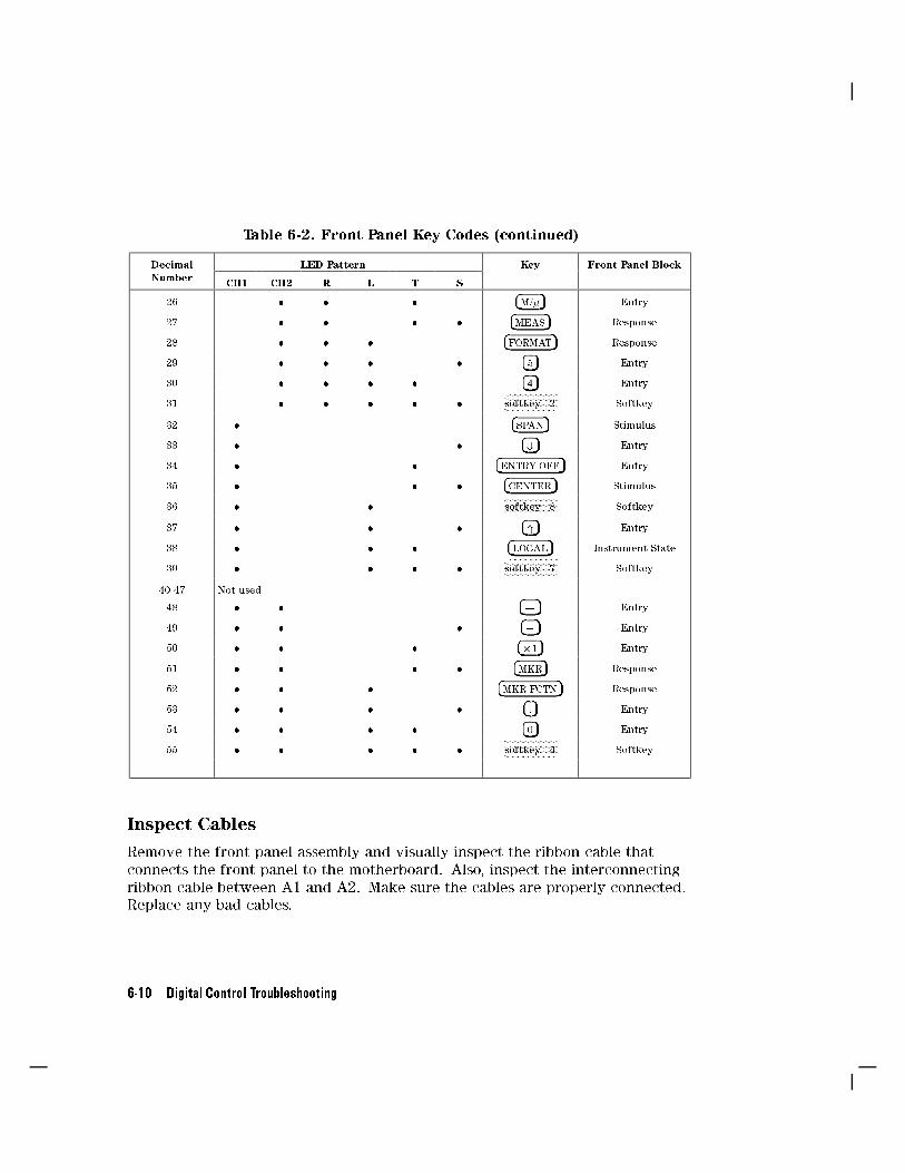
Table 6-2. Front Panel Key Codes (continued)
Decimal
Number
LED Pattern Key Front Panel Block
CH1 CH2 R L T S
26 � � � �M/�� Entry
27 � � � � �MEAS� Response
28 � � � �FORMAT� Response
29 � � � � �5� Entry
30 � � � � �4� Entry
31 � � � � �???????????????????softkey 2 Softkey
32 � �SPAN� Stimulus
33 � � �+� Entry
34 � � �ENTRY OFF� Entry
35 � � � �CENTER� Stimulus
36 � �???????????????????softkey 8 Softkey
37 � � � �*� Entry
38 � � � �LOCAL� Instrument State
39 � � � �???????????????????softkey 7 Softkey
40-47 Not used
48 � � � � Entry
49 � � � ��� Entry
50 � � � ��1� Entry
51 � � � � �MKR� Response
52 � � � �MKR FCTN� Response
53 � � � � �.� Entry
54 � � � � �0� Entry
55 � � � � �???????????????????softkey 4 Softkey
Inspect Cables
Remove the front panel assembly and visually inspect the ribbon cable thatconnects the front panel to the motherboard. Also, inspect the interconnecting
ribbon cable between A1 and A2. Make sure the cables are properly connected.Replace any bad cables.
6-10 Digital Control Troubleshooting

Test Using a Controller
If a controller is available, write a simple command to the analyzer. If theanalyzer successfully executes the command, the problem is either the A2 frontpanel interface or W17 (A2 to motherboard ribbon cable) is faulty.
Run the Internal Diagnostic Tests
The analyzer incorporates 20 internal diagnostic tests. Most tests can be run aspart of one or both major test sequences: all internal (test 0) and preset (test 1).
1. Press �SYSTEM�NNNNNNNNNNNNNNNNNNNNNNNNNNNNNNNNNNNNNNSERVICE MENU
NNNNNNNNNNNNNNNNNTESTS �0� ��1�
NNNNNNNNNNNNNNNNNNNNNNNNNNNNNNNNNNNNNNEXECUTE TEST to perform All
INT tests.
2. Then press �1� ��1� to see the results of the preset test. If either sequence
fails, press the �*� �+� keys to �nd the �rst occurrence of a FAIL message for
tests 2 through 20. See Table 6-3 for further troubleshooting information.
Digital Control Troubleshooting 6-11

Table 6-3. Internal Diagnostic Test with Commentary
Test Sequence* Probable Failed Assembliesy;
Comments and Troubleshooting Hints
0 All Int |- |: Executes tests 3-11, 13-16, 20.
1 Preset |- |: Executes tests 2-11, 14-16. Runs at power-on or preset.
2 ROM P,AI A9: Repeats on fail; refer to \Check A9 CPU Operation" in this chapter
to replace ROM or A9.
3 CMOS RAM P,AI A9: Replace A9.
4 Main DRAM P,AI A9: Repeats on fail; replace A9.
5 DSP Wr/Rd P,AI A9: Replace A9.
6 DSP RAM P,AI A9: Replace A9.
7 DSP ALU P,AI A9: Replace A9.
8 DSP Intrpt P,AI A9/A10: Remove A10, rerun test. If fail, replace A9. If pass, replace A10.
9 DIF Control P,AI A9/A10: Most likely A9 assembly.
10 DIF Counter P,AI A10/A9/A12: Check analog bus node 17 for 1 MHz. If correct, A12 is
veri�ed; suspect A10.
11 DSP Control P,AI A10/A9: Most likely A10.
12 Fr Pan Wr/Rd |- A2/A1/A9: Run test 23. If fail, replace A2. If pass, problem is on bus
between A9 and A2 or on A9 assembly.
13 Rear Panel AI A16/A9: Disconnect A16, and check A9J2 pin 48 for 4 MHz clock signal.
If OK, replace A16. If not, replace A9.
14 Post-reg P,AI A15/A8/Destination assembly: Refer to the \Power Supply
Troubleshooting" chapter.
15 Frac-N Cont P,AI A14: Replace A14.
16 Sweep Trig P,AI A14,A10: Most likely A14.
17 ADC Lin |- A10: Replace A10.
18 ADC Ofs |- A10: Replace A10.
19 ABUS Test |- A10: Replace A10.
20 FN Count AI A14/A13/A10: Most likely A14 or A13, as previous tests check A10.
Refer to the \Source Troubleshooting" chapter.
* P = part of PRESET sequence; AI =part of ALL INTERNAL sequence.y in decreasing order of probability.
6-12 Digital Control Troubleshooting
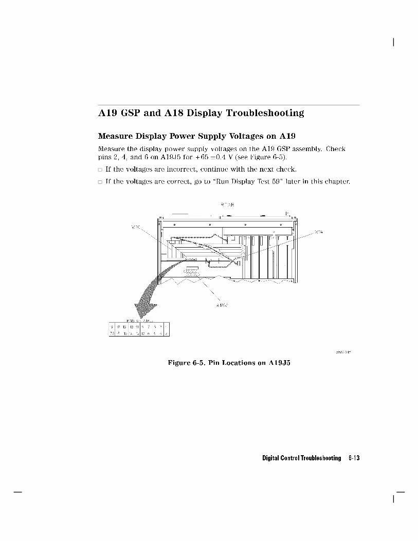
A19 GSP and A18 Display Troubleshooting
Measure Display Power Supply Voltages on A19
Measure the display power supply voltages on the A19 GSP assembly. Checkpins 2, 4, and 6 on A19J5 for +65 �0.4 V (see Figure 6-5).
If the voltages are incorrect, continue with the next check.
If the voltages are correct, go to \Run Display Test 59" later in this chapter.
Figure 6-5. Pin Locations on A19J5
Digital Control Troubleshooting 6-13

Measure Display Power Supply Voltages Entering A19
Measure the power supply voltages entering the A19 assembly coming from theA8 assembly. Check pins 1 and 2 on the connector of W14 for +65 �0.4 V, andpin 6 for +5.16 �0.1 V (see Figure 6-6).
If the voltages are incorrect, refer to the \Power Supply Troubleshooting"chapter.
If the voltages are correct entering, but incorrect leaving the GSP assembly,
replace the A19 GSP assembly.
Figure 6-6. Pin Locations on Connector of W14
6-14 Digital Control Troubleshooting

Run Display Test 59
1. On the analyzer, press �PRESET� �SYSTEM�NNNNNNNNNNNNNNNNNNNNNNNNNNNNNNNNNNNNNNSERVICE MENU (softkey 8)
NNNNNNNNNNNNNNNNNTESTS
(softkey 1)NNNNNNNNNNNNNNNNNNNNNNNNNNNNNNNNNNNNNNNNNDISPLAY TESTS (softkey 7). The analyzer will display:
TEST
59 Disp/cpu com -ND-
2. PressNNNNNNNNNNNNNNNNNNNNNNNNNNNNNNNNNNNNNNEXECUTE TEST (softkey 8). The display will blank and the front panel
LEDs will ash once.
If all of the LEDs go o� and the display remains blank the analyzer passedthe test. If the analyzer passes the test, press �PRESET� and go to \Run
display Tests 60-65".
If any of the front panel LEDs remain on (except for the port LEDs), theanalyzer failed the test. Continue with the next check.
Inspect Ribbon Cable Repeat Display Test 59
1. Inspect the W20 (A9-A19) ribbon cable for a loose connection.
2. Repeat \Run Display test 59." If the test fails, a walking one pattern will be
continuously transferred from the CPU, through the cable, to the GSP.
3. Immediately go to the next check.
Digital Control Troubleshooting 6-15

Perform Walking One Pattern
1. Disconnect the W20 (A9-A19) ribbon cable from A19J6.
2. Use an oscilloscope to verify a walking one pattern is transferring fromthe A9 CPU through the cable. The walking one pattern (see Figure 6-7) isfound on pins 3 through 10, and 13 through 20 on the connector of W20 (seeFigure 6-8).
If the signal is not present at the end of the cable, check for it at the A9connector of the ribbon cable.
If the signal is still not present, replace the A9 assembly.
Figure 6-7. A9 CPU Walking One Pattern
6-16 Digital Control Troubleshooting

Figure 6-8. Pin Locations on Connector of W20
Run display Tests 60-65
1. Press �PRESET� �SYSTEM�NNNNNNNNNNNNNNNNNNNNNNNNNNNNNNNNNNNNNNSERVICE MENU (softkey 8)
NNNNNNNNNNNNNNNNNTESTS (softkey 1)
NNNNNNNNNNNNNNNNNNNNNNNNNNNNNNNNNNNNNNNNNDISPLAY TESTS (softkey 7) �60� ��1�.
2. PressNNNNNNNNNNNNNNNNNNNNNNNNNNNNNNNNNNNNNNEXECUTE TEST (softkey 8). If the analyzer passes the test, the display
will blank and the front panel LEDs will ash once.
3. Press �PRESET� and perform display tests 61 through 65 (substitute the next
test number where �60� was used). Watch for the LEDs to go o� and thedisplay to blank except for test 65. Test 65 causes the display to dim ratherthan blank.
If any of the display tests fail, replace the A19 assembly.
If all of the following is true, replace the A18 display assembly.
CPU test passes the LED test.
GSP passes all of the internal display tests (59 through 65).
Power supply checks out.
Intensity, focus, and vertical adjustments fail to produce an acceptableimage.
Digital Control Troubleshooting 6-17

If the Fault is Intermittent
Repeat Test Function
If the failure is intermittent, do the following:
1. Press �SYSTEM�NNNNNNNNNNNNNNNNNNNNNNNNNNNNNNNNNNNNNNSERVICE MENU
NNNNNNNNNNNNNNNNNNNNNNNNNNNNNNNNNNNNNNTEST OPTIONS
NNNNNNNNNNNNNNNNNNNNNNNNNNNNNREPEAT ON to activate the
repeat function.
2. Then pressNNNNNNNNNNNNNNNNNNNNRETURN
NNNNNNNNNNNNNNNNNTESTS .
3. Select the desired test and pressNNNNNNNNNNNNNNNNNNNNNNNNNNNNNNNNNNNNNNEXECUTE TEST .
4. Press �PRESET� to stop the function. The test repeat function is explained in
the \Service Key Menus and Error Messages" chapter.
HP-IB Failures
If you have performed \Step 3. Troubleshooting HP-IB Systems" in the \StartTroubleshooting Here" chapter, and you suspect there is an HP-IB problem in
the analyzer, perform the following test. It checks the internal communication
path between the A9 CPU and the A16 rear panel. It does not check the HP-IBpaths external to the analyzer.
Press �SYSTEM�NNNNNNNNNNNNNNNNNNNNNNNNNNNNNNNNNNNNNNSERVICE MENU
NNNNNNNNNNNNNNNNNTESTS �13� ��1�
NNNNNNNNNNNNNNNNNNNNNNNNNNNNNNNNNNNNNNEXECUTE TEST .
If the analyzer fails the test, the problem is likely to be the A16 rear panel.
If the analyzer passes the test, it indicates that the A9 CPU can communicatewith the A16 rear panel with a 50% con�dence level. There is a good chancethat the A16 rear panel is working. This is because internal bus lines havebeen tested between the A9 CPU and A16, and HP-IB signal paths are notchecked external to the analyzer.
6-18 Digital Control Troubleshooting
7
Source Troubleshooting
Use this procedure only if you have read the \Start Troubleshooting Here"chapter. This chapter is divided into two troubleshooting procedures for thefollowing problems:
Incorrect power levels: Perform the \Power" troubleshooting checks.
Phase lock error: Perform the \Phase Lock Error" troubleshooting checks.
The source group assemblies consist of the following:
A3 source
A4 sampler/mixer
A7 pulse generator
A11 phase lock
A12 reference
A13 fractional-N (analog)
A14 fractional-N (digital)
Source Troubleshooting 7-1

Assembly Replacement Sequence
The following steps show the sequence to replace an assembly in an HP 8752CNetwork Analyzer.
1. Identify the faulty group. Refer to the \Start Troubleshooting Here" chapter.Follow up with the appropriate troubleshooting chapter that identi�es thefaulty assembly.
2. Order a replacement assembly. Refer to the \Replaceable Parts" chapter.
3. Replace the faulty assembly and determine what adjustments are necessary.Refer to the \Assembly Replacement and Post-Repair Procedures" chapter.
4. Perform the necessary adjustments. Refer to the \Adjustments and
Correction Constants" chapter.
5. Perform the necessary performance tests. Refer to the \System Veri�cationand Performance Tests" chapter.
Before You Start Troubleshooting
Make sure all of the assemblies are �rmly seated. Also make sure that input Rhas a signal of at least �35 dBm (about 0.01 Vp-p into 50 ohms) at all times to
maintain phase lock.
7-2 Source Troubleshooting

Power
If the analyzer output power levels are incorrect but no phase lock error ispresent, perform the following checks in the order given:
1. Source Default Correction Constants (Test 44)
1. Press �PRESET� �SYSTEM�NNNNNNNNNNNNNNNNNNNNNNNNNNNNNNNNNNNNNNSERVICE MENU
NNNNNNNNNNNNNNNNNTESTS �44� ��1�
NNNNNNNNNNNNNNNNNNNNNNNNNNNNNNNNNNNNNNEXECUTE TEST .
When complete, \DONE" should appear on the analyzer display.
2. Use a power meter to verify that source power can be controlled and thatthe power level is approximately correct.
If the source passes these checks, proceed with step 2.
If \FAIL" appears on the analyzer display, or if the analyzer fails the
checks, replace the source.
2. RF Output Power Correction Constants (Test 47)
1. Follow the instructions for this procedure given in the \Adjustments and
Correction Constants" chapter. The procedure is complete when \DONE"
appears on the analyzer display.
2. Use a power meter to verify that power levels are now correct.
If power levels are incorrect, or if the analyzer fails the routine, proceed
with step 3.
3. Sampler Magnitude and Phase Correction Constants(Test 53)
1. Follow the instructions for this procedure given in the \Adjustments andCorrection Constants" chapter. The procedure is complete when \DONE"appears on the analyzer display.
2. Repeat step 2.
If the analyzer fails the routine in step 2, replace the source.
If the analyzer fails the routine in step 3, replace the source.
Source Troubleshooting 7-3
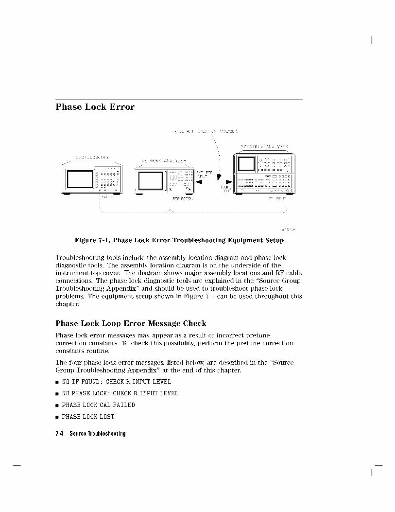
Phase Lock Error
Figure 7-1. Phase Lock Error Troubleshooting Equipment Setup
Troubleshooting tools include the assembly location diagram and phase lockdiagnostic tools. The assembly location diagram is on the underside of theinstrument top cover. The diagram shows major assembly locations and RF cable
connections. The phase lock diagnostic tools are explained in the \Source Group
Troubleshooting Appendix" and should be used to troubleshoot phase lock
problems. The equipment setup shown in Figure 7-1 can be used throughout thischapter.
Phase Lock Loop Error Message Check
Phase lock error messages may appear as a result of incorrect pretunecorrection constants. To check this possibility, perform the pretune correctionconstants routine.
The four phase lock error messages, listed below, are described in the \Source
Group Troubleshooting Appendix" at the end of this chapter.
NO IF FOUND: CHECK R INPUT LEVEL
NO PHASE LOCK: CHECK R INPUT LEVEL
PHASE LOCK CAL FAILED
PHASE LOCK LOST
7-4 Source Troubleshooting

1. Make sure the A9 CC Jumper is in the ALTER position:
a. Unplug the analyzer.
b. Remove the top cover.
c. Remove the A9 CPU board.
d. Move the jumper to the ALT position. (Refer to Figure 7-2.)
e. Replace the A9 CPU board, top cover, and power cord.
Figure 7-2. Jumper Positions on the A9 CPU
Source Troubleshooting 7-5

2. Switch on the analyzer and press �PRESET� �SYSTEM�NNNNNNNNNNNNNNNNNNNNNNNNNNNNNNNNNNNNNNSERVICE MENU
NNNNNNNNNNNNNNNNNTESTS
�46� ��1�NNNNNNNNNNNNNNNNNNNNNNNNNNNNNNNNNNNNNNEXECUTE TEST
NNNNNNNNNNNYES to generate new analog bus correction
constants.
3. Then press �PRESET� �SYSTEM�NNNNNNNNNNNNNNNNNNNNNNNNNNNNNNNNNNNNNNSERVICE MENU
NNNNNNNNNNNNNNNNNTESTS �45� ��1�
NNNNNNNNNNNNNNNNNNNNNNNNNNNNNNNNNNNNNNEXECUTE TEST
NNNNNNNNNNNYES to generate new pretune correction constants.
4. Press �PRESET� �SYSTEM�NNNNNNNNNNNNNNNNNNNNNNNNNNNNNNNNNNNNNNSERVICE MENU
NNNNNNNNNNNNNNNNNTESTS �48� ��1�
NNNNNNNNNNNNNNNNNNNNNNNNNNNNNNNNNNNNNNEXECUTE TEST
NNNNNNNNNNNYES
to generate new pretune correction constants.
Note Always press �PRESET� before and after performing anadjustment test.
5. Press �PRESET� and observe the analyzer display:
If no error message is displayed: restore the A9 CC jumper to the NRMposition. Then refer to \Post-Repair Procedures" in the \Assembly
Replacement and Post-Repair Procedures" chapter to verify operation.
If an error message is displayed: continue with \A4 Sampler/Mixer Check."
A4 Sampler/Mixer Check
The A4, A5, and A6 (R, A and B) sampler/mixers are similar in operation. Anysampler can be used to phase lock the source. To eliminate the possibility of a
faulty R sampler, follow this procedure.
1. Remove the W8 cable (A11J1 to A4) from the R-channel sampler (A4) and
connect it to either the A-channel sampler (A5) or the B-channel sampler
(A6). Refer to Figure 7-3.
7-6 Source Troubleshooting

Figure 7-3. Sampler/Mixer to Phase Lock Cable Connection Diagram
2. If you connected W8 to:
A5, press �MEAS�NNNNNNNNNNNNNNNNNNNNNNNNNNNNNNNNREFLECTION
A6, connect a cable between the re ection and transmission test ports and
press �MEAS�NNNNNNNNNNNNNNNNNNNNNNNNNNNNNNNNTRANSMISSN
3. Ignore the displayed trace, but check for phase lock error messages. If the
phase lock problem persists, the R-channel sampler is not the problem.
Source Troubleshooting 7-7

A3 Source and A11 Phase Lock Check
This procedure checks the source and part of the phase lock assembly. It opensthe phase-locked loop and exercises the source by varying the source outputfrequency with the A11 pretune DAC.
Note If the analyzer failed internal test 48, default pretune correctionconstants were stored which may result in a constant o�set ofseveral MHz. Regardless, continue with this procedure.
Note Use a spectrum analyzer for problems above 100 MHz.
1. Connect the oscilloscope or spectrum analyzer as shown in Figure 7-1. (Setthe oscilloscope input impedance to 50 ohms.)
2. Press �PRESET� �SYSTEM�NNNNNNNNNNNNNNNNNNNNNNNNNNNNNNNNNNNNNNSERVICE MENU
NNNNNNNNNNNNNNNNNNNNNNNNNNNNNNNNNNNNNNNNNSERVICE MODES
NNNNNNNNNNNNNNNNNNNNNNNNNNNNNNNNNNNNNNNNNNNNNNNSRC ADJUST MENU
NNNNNNNNNNNNNNNNNNNNNNNNNNNNNNNNNNNSRC TUNE ON
NNNNNNNNNNNNNNNNNNNNNNNNNNNNNNNNNNNNNNNNNSRC TUNE FREQ to activate the source tune (SRC TUNE)
service mode.
3. Use the front panel knob or front panel keys to set the pretune frequencyto 300 kHz, 30 MHz, and 40 MHz. Verify the signal frequency on theoscilloscope.
Note In SRC TUNE mode, the source output frequency changes in
1 to 2 MHz increments and should be 1 to 6 MHz above theindicated output frequency.
4. Check for the frequencies indicated by Table 7-1.
Table 7-1. Output Frequency in SRC Tune Mode
Setting Observed Frequency
300 kHz 1.3 to 6.3 MHz
30 MHz 31 to 36 MHz
40 MHz 41 to 46 MHz
7-8 Source Troubleshooting

5. The signal observed on an oscilloscope should be as solid as the signal inFigure 7-4.
Figure 7-4. Waveform Integrity in SRC Tune Mode
6. The signal observed on the spectrum analyzer will appear jittery as inFigure 7-5b, not solid as in Figure 7-5a. This is because in SRC TUNE modethe output is not phase locked.
Figure 7-5.Phase Locked Output Compared to Open Loop Output in SRC Tune Mode
Source Troubleshooting 7-9

7. Press �MENU�NNNNNNNNNNNNNNNNNPOWER to vary the power and check for corresponding level
changes on the test instrument. (A power change of 20 dB will change thevoltage observed on the oscilloscope by a factor of ten.)
8. Note the results of the frequency and power changes:
If the frequency and power output changes are correct, continue with\A12 Reference Check" located in this chapter.
If the frequency changes are incorrect, continue with \YO Coil Drive Checkwith Analog Bus."
If the power output changes are incorrect, check analog bus node 3.
a. Press �SYSTEM�NNNNNNNNNNNNNNNNNNNNNNNNNNNNNNNNNNNNNNSERVICE MENU
NNNNNNNNNNNNNNNNNNNNNNNNNNNNNNNNNNNNNNNNNANALOG BUS ON �MEAS�NNNNNNNNNNNNNNNNNNNNNNNNNNNNNNNNNNNNNNNNNNNNNNNNNNNNNNNNNNN
ANALOG IN Aux Input �FORMAT�NNNNNNNNNNNNNNMORE
NNNNNNNNNNNNNNREAL �3� ��1�.
b. Press �MARKER� �2� �G/n�. The marker should read approximately 434 mU.
c. Press �MARKER� �4� �G/n�. The marker should read approximately 646 mU.
7-10 Source Troubleshooting

YO Coil Drive Check with Analog Bus
Note If the analog bus is not functional, perform the \YO Drive CoilCheck with Oscilloscope" procedure.
1. Press �PRESET� �SYSTEM�NNNNNNNNNNNNNNNNNNNNNNNNNNNNNNNNNNNNNNSERVICE MENU
NNNNNNNNNNNNNNNNNNNNNNNNNNNNNNNNNNNNNNNNNANALOG BUS ON
NNNNNNNNNNNNNNNNNNNNNNNNNNNNNNNNNNNNNNNNNSERVICE MODES
NNNNNNNNNNNNNNNNNNNNNNNNNNNNNNNNNNNNNNNNNNNNSOURCE PLL OFF �MEAS�
NNNNNNNNNNNNNNNNNNNNNNNNNNNNNNNNNNNNNNNNNNNNNNNNNNNNNNNNNNNANALOG IN Aux Input
NNNNNNNNNNNNNNNNNNNNNNNNNNNNNNNNNNNNNNNNNNNNNNNNNNNNNNNNNNNCOUNTER: ANALOG BUS .
2. Then press �16� ��1� �FORMAT�NNNNNNNNNNNNNNMORE
NNNNNNNNNNNNNNREAL �SCALE REF�
NNNNNNNNNNNNNNNNNNNNNNNNNNNNNAUTOSCALE . This
keystroke sequence lets you check the pretune DAC and the A11 output tothe YO coil drive by monitoring the 1V/GHz signal at analog bus node 16.
3. Compare the waveform to Figure 7-6. If the waveform is incorrect, the A11phase lock assembly is faulty.
Figure 7-6. 1V/GHz at Analog Bus Node 16 with Source PLL O�.
Source Troubleshooting 7-11

YO Coil Drive Check with Oscilloscope
Note Use the large extender board for easy access to the voltagepoints. The extender board is included with the HP 8753 ToolKit. See the \Replaceable Parts" chapter for part numbers andordering information.
1. Connect oscilloscope probes to A11P1-1 and A11P1-2. The YO coil drivesignal is actually two signals whose voltage di�erence drives the coil.
2. Press �PRESET� �SYSTEM�NNNNNNNNNNNNNNNNNNNNNNNNNNNNNNNNNNNNNNSERVICE MENU
NNNNNNNNNNNNNNNNNNNNNNNNNNNNNNNNNNNNNNNNNSERVICE MODES
NNNNNNNNNNNNNNNNNNNNNNNNNNNNNNNNNNNNNNNNNNNNSOURCE PLL OFF to
operate the analyzer in a swept open loop mode.
3. Monitor the two YO coil drive lines. In source tune mode the voltage
di�erence should vary from approximately 3.5 to 5.0 volts as shown inFigure 7-7.
If the voltages are incorrect, replace the faulty A11 assembly.
If the voltages are correct, replace the faulty A3 source assembly.
If neither the A11, nor the A3 assembly is faulty, continue with the nextcheck.
Figure 7-7.YO� and YO+ Coil Drive Voltage Di�erences with SOURCE PLL OFF
7-12 Source Troubleshooting

A12 Reference Check
The signals are evaluated with pass/fail checks. The most e�cient way to checkthe A12 frequency reference signals is to use the analog bus while referring toTable 7-2.
Alternatively, you can use an oscilloscope, while referring to Table 7-3 andFigure 7-8 through Figure 7-14. If any of the observed signals di�ers fromthe �gures, there is a 90% probability that the A12 assembly is faulty. Eitherconsider the A12 assembly defective or perform the \A12 Digital Control SignalsCheck."
Both of these procedures are described next.
Analog Bus Method
1. Press �PRESET� �SYSTEM�NNNNNNNNNNNNNNNNNNNNNNNNNNNNNNNNNNNNNNSERVICE MENU
NNNNNNNNNNNNNNNNNNNNNNNNNNNNNNNNNNNNNNNNNANALOG BUS ON �MEAS�NNNNNNNNNNNNNNNNNNNNNNNNNNNNNNNNNNNNNNNNNNNNNNNNNNNNNNNNNNN
ANALOG IN Aux InputNNNNNNNNNNNNNNNNNNNNNNNNNNNNNNNNANALOG BUS to switch on the analog bus and its
counter.
2. Press �21� ��1� to count the frequency of the 100 kHz signal.
3. Press �MENU�NNNNNNNNNNNNNNNNNNNNNNNCW FREQ �500� �k/m�. Verify that the counter reading (displayed
on the analyzer next to cnt:) matches the corresponding 100 kHz value for
the CW frequency. (Refer to Table 7-2.)
4. Verify the remaining CW frequencies, comparing the counter reading withthe value in Table 7-2:
a. Press �2� �M/��.
b. Press �50� �M/��.
Table 7-2. Analog Bus Check of Reference Frequencies
CW Frequency Analog Bus Node 21
100 kHz
Analog Bus Node 24
2nd LO
Analog Bus Node 25
PLREF
500 kHz 0.100 MHz 0.504 MHz 0.500 MHz
2 MHz 0.100 MHz 2.007 MHz 2.000 MHz
50 MHz 0.100 MHz 0.996 MHz 1.000 MHz
NOTE: The counter should indicate the frequencies listed in this table to within �0.1%. Accuracy may vary
with gate time and signal strength.
Source Troubleshooting 7-13

5. Press �24� ��1� to count the frequency of the 2nd LO signal.
6. Press �MENU�NNNNNNNNNNNNNNNNNNNNNNNCW FREQ �500� �k/m�. Verify that the counter reading matches
the corresponding 2nd LO value for the CW frequency. (Refer to Table 7-2.)
7. Verify the remaining CW frequencies, comparing the counter reading withthe value in Table 7-2:
a. Press �2� �M/��.
b. Press �50� �M/��.
8. Press �25� ��1� to count the frequency of the PLREF signal.
9. Press �MENU�NNNNNNNNNNNNNNNNNNNNNNNCW FREQ �500� �k/m�. Verify that the counter reading matches
the corresponding PLREF value for the CW frequency. (Refer to Table 7-2.)
10. Verify the remaining CW frequencies, comparing the counter reading with
the value in Table 7-2:
a. Press �2� �M/��.
b. Press �50� �M/��.
11. Check the results.
If all the counter readings match the frequencies listed in Table 7-2,continue with \A13/A14 Fractional-N Check."
If the counter readings are incorrect at the 500 kHz and 2 MHz settingsonly, continue with \FN LO at A12 Check."
If all the counter readings are incorrect at all three CW frequencies, the
counter may be faulty. Perform the \Oscilloscope Method" check of thesignals described below. (If the signals are correct, either the A10 or A14assemblies could be faulty.)
7-14 Source Troubleshooting

Oscilloscope Method
You need not use the oscilloscope method unless the analog bus isnon-functional or any of the signals fail the speci�cations listed in Table 7-2.
If the analog bus is non-functional or the previous check has revealedquestionable signals, observe the signal(s) with an oscilloscope. Table 7-3identi�es convenient test points and �gures showing the �ve signals listed.
Table 7-3. A12 Reference Frequencies
Mnemonic Signal
Description
Test Point
Location
See
Figure
Analyzer
Setting
FN100kHzREF 100 kHz Reference A13TP5 Figure 7-8 any
REF Phase Lock
Reference
A11TP1 PIN 9 Figure 7-9 �16 MHz CW
REF Phase Lock
Reference
A11TP1 PIN 9 Figure 7-10 5 MHz CW
FN LO* Fractional-N LO A14J2 Figure 7-11 10 MHz CW
4MHz REF 4 MHz Reference A12TP9 Figure 7-12 any
2ND LO+/� Second LO A12P1-2,4 Figure 7-13 �16 MHz CW
2ND LO+/� Second LO A12P1-2,4 Figure 7-14 14 MHz CW
* not an A12 signal, but required for A12 lowband operation.
Source Troubleshooting 7-15

100 kHz Pulses
The 100 kHz pulses are very narrow and typically 1.5V in amplitude. You mayhave to increase the oscilloscope intensity to see these pulses. (See Figure 7-8.)
Figure 7-8. Sharp 100 kHz Pulses at A13TP5 (any frequency)
7-16 Source Troubleshooting

PLREF Waveforms
REF Signal At A11TP1 PIN 9. REF is the bu�ered PLREF+ signal. The 1st IFis phase locked to this signal. Use an oscilloscope to observe the signal at thefrequencies noted in Figure 7-9 and Figure 7-10.
High Band REF Signal. In high band the REF signal is a constant 1 MHz squarewave as indicated by Figure 7-9.
Figure 7-9. High Band REF Signal (�16 MHz CW)
Source Troubleshooting 7-17

Low Band REF Signal. In low band this signal follows the frequency of the RFoutput signal. Figure 7-10 illustrates a 5 MHz CW signal.
Figure 7-10. REF Signal at A11TP9 (5 MHz CW)
If REF looks correct, continue with \4 MHz Reference Signal."
If REF is incorrect in low band, continue with \FN LO at A12 Check."
7-18 Source Troubleshooting
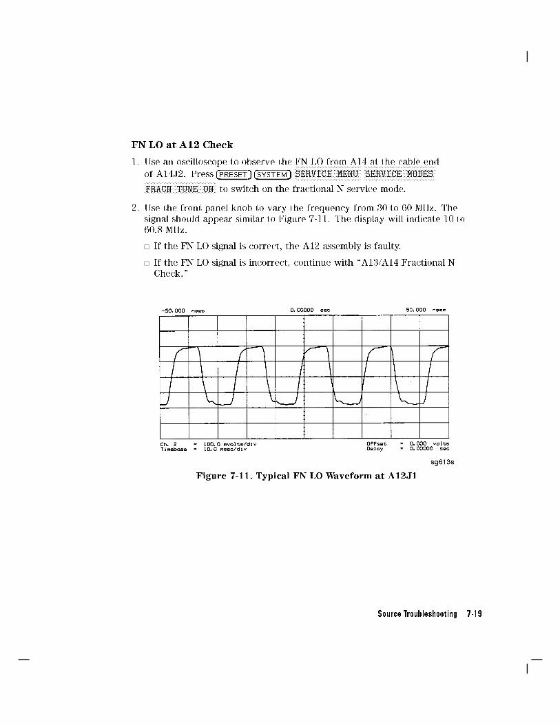
FN LO at A12 Check
1. Use an oscilloscope to observe the FN LO from A14 at the cable end
of A14J2. Press �PRESET� �SYSTEM�NNNNNNNNNNNNNNNNNNNNNNNNNNNNNNNNNNNNNNSERVICE MENU
NNNNNNNNNNNNNNNNNNNNNNNNNNNNNNNNNNNNNNNNNSERVICE MODES
NNNNNNNNNNNNNNNNNNNNNNNNNNNNNNNNNNNNNNNNNFRACN TUNE ON to switch on the fractional-N service mode.
2. Use the front panel knob to vary the frequency from 30 to 60 MHz. Thesignal should appear similar to Figure 7-11. The display will indicate 10 to60.8 MHz.
If the FN LO signal is correct, the A12 assembly is faulty.
If the FN LO signal is incorrect, continue with \A13/A14 Fractional-NCheck."
Figure 7-11. Typical FN LO Waveform at A12J1
Source Troubleshooting 7-19

4 MHz Reference Signal
This reference signal is used to control the receiver. If faulty, this signal cancause apparent source problems because the CPU uses receiver data to controlthe source. At A12TP9 it should appear similar to Figure 7-12.
Figure 7-12. 4 MHz Reference Signal at A12TP9 (Preset)
7-20 Source Troubleshooting

2ND LO Waveforms
The 2nd LO signals appear di�erent in phase and shape at di�erent frequencies.Refer to Table 7-3 for convenient test points.
90 Degree Phase O�set of 2nd LO Signals in High Band. In high band, the2nd LO is 996 kHz. As indicated by Figure 7-13, the 2nd LO actually consists oftwo signals 90 degrees out of phase.
Figure 7-13.90 Degree Phase O�set of High Band 2nd LO Signals (�16 MHz CW)
Source Troubleshooting 7-21

In-Phase 2nd LO Signals in Low Band. The 2nd LO signals in low band, asshown in Figure 7-14, are not phase shifted. In low band these signals track theRF output with a 4 kHz o�set.
Figure 7-14. In-Phase Low Band 2nd LO Signals (14 MHz CW)
If any of the signals of Table 7-2 are incorrect, the probability is 90% that theA12 assembly is faulty. Either consider the A12 assembly faulty or perform the
\A12 Digital Control Signals Check" described next.
7-22 Source Troubleshooting

A12 Digital Control Signals Check
Several digital control signals must be functional for the A12 assemblyto operate correctly. Check the control lines listed in Table 7-4 with theoscilloscope in the high input impedance setting.
Table 7-4. A12-Related Digital Control Signals
Mnemonic Signal
Description
Location See
Figure
Analyzer
Setting
L ENREF L=Reference Enable A12P2-16 Figure 7-15 Preset
L HB L=High Band A12P2-32 Figure 7-16 Preset
L LB L=Low Band A12P1-23 Figure 7-16 Preset
L ENREF Line. This is a TTL signal. To observe it, trigger on the negative edge.
In preset state, the signal should show activity similar to Figure 7-15.
Figure 7-15. L ENREF Line at A12P2-16 (Preset)
Source Troubleshooting 7-23

L HB and L LB Lines. These complementary signals toggle when the instrumentswitches from low band to high band as illustrated by Figure 7-16.
Figure 7-16. Complementary L HB and L LB Signals (Preset)
If all of the digital signals appeared correct, the A12 assembly is faulty.
A13/A14 Fractional-N Check
Use the analog bus or an oscilloscope to check the A14 VCO's ability to sweepfrom 30 MHz to 60 MHz. The faster analog bus method should su�ce unlessproblems are detected.
Fractional-N Check with Analog Bus
1. Press �PRESET� �SYSTEM�NNNNNNNNNNNNNNNNNNNNNNNNNNNNNNNNNNNNNNSERVICE MENU
NNNNNNNNNNNNNNNNNNNNNNNNNNNNNNNNNNNNNNNNNANALOG BUS ON �MEAS�NNNNNNNNNNNNNNNNNNNNNNNNNNNNNNNNNNNNNNNNNNNNNNNNNNNNNNNNNNN
ANALOG IN Aux InputNNNNNNNNNNNNNNNNNNNNFRAC N to switch on the analog bus and the
fractional-N counter.
2. Then press �MENU�NNNNNNNNNNNNNNNNNNNNNNNCW FREQ to set the analyzer to CW mode.
3. Set the instrument as indicated in Table 7-5 and see whether the VCO
generates the frequencies listed.
7-24 Source Troubleshooting
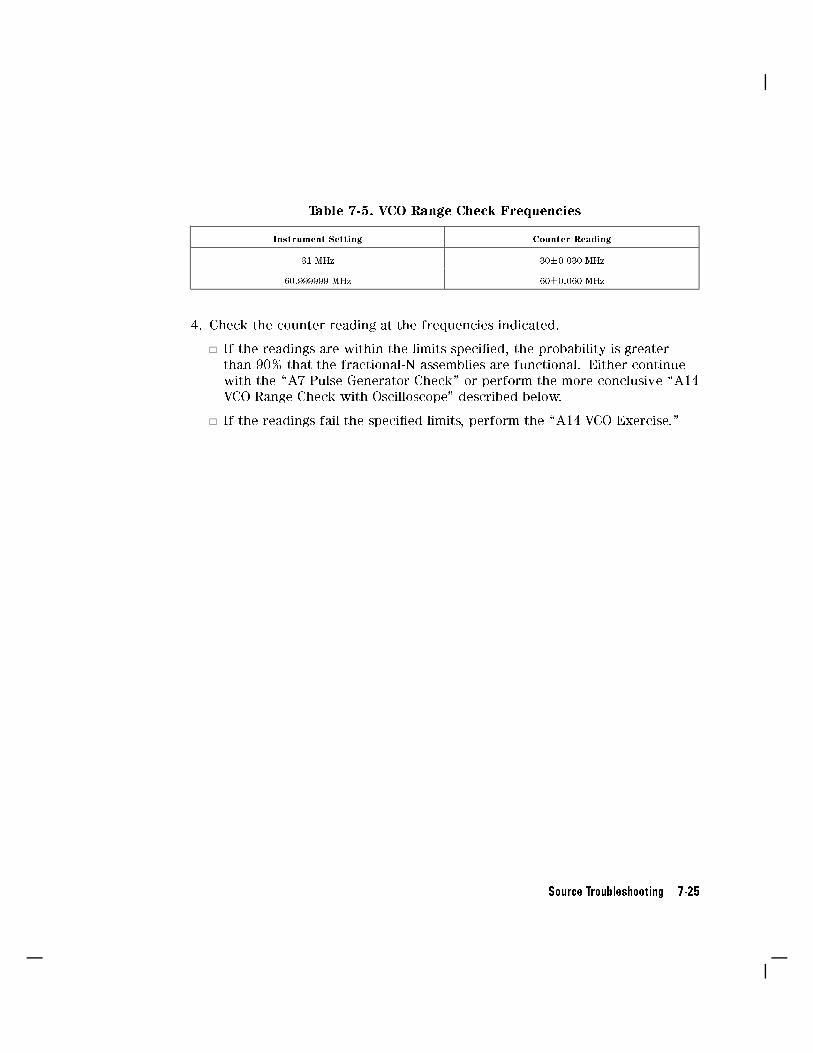
Table 7-5. VCO Range Check Frequencies
Instrument Setting Counter Reading
31 MHz 30�0.030 MHz
60.999999 MHz 60�0.060 MHz
4. Check the counter reading at the frequencies indicated.
If the readings are within the limits speci�ed, the probability is greaterthan 90% that the fractional-N assemblies are functional. Either continuewith the \A7 Pulse Generator Check" or perform the more conclusive \A14VCO Range Check with Oscilloscope" described below.
If the readings fail the speci�ed limits, perform the \A14 VCO Exercise."
Source Troubleshooting 7-25

A14 VCO Range Check with Oscilloscope
1. Remove the W9 HI OUT cable (A14J1 to A7) from the A7 assembly andconnect it to an oscilloscope set for 50 ohm input impedance. Switch on theanalyzer.
2. Press �PRESET� �SYSTEM�NNNNNNNNNNNNNNNNNNNNNNNNNNNNNNNNNNNNNNSERVICE MENU
NNNNNNNNNNNNNNNNNNNNNNNNNNNNNNNNNNNNNNNNNSERVICE MODES
NNNNNNNNNNNNNNNNNNNNNNNNNNNNNNNNNNNNNNNNNFRACN TUNE ON to
activate the FRACN TUNE service mode. See the \Service Key Menus andError Messages" chapter for more information on the FRACN TUNE mode.
3. Vary the fractional-N VCO frequency with the front panel knob and checkthe signal with the oscilloscope. The waveform should resemble Figure 7-17,
Figure 7-18, and Figure 7-19.
If the fractional-N output signals are correct, continue source troubleshootingby continuing with \A7 Pulse Generator Check."
Figure 7-17. 10 MHz HI OUT Waveform from A14J1
7-26 Source Troubleshooting

Figure 7-18. 25 MHz HI OUT Waveform from A14J1
Figure 7-19. 60 MHz HI OUT Waveform from A14J1
Source Troubleshooting 7-27

A14 VCO Exercise
The nominal tuning voltage range of the VCO is +10 to �5 volts. When theanalyzer is in operation, this voltage is supplied by the A13 assembly. Thisprocedure substitutes a power supply for the A13 assembly to check thefrequency range of the A14 VCO.
1. Switch o� the analyzer and remove the A13 assembly.
2. Put the A14 assembly on an extender board and switch on the instrument.
3. Prepare to monitor the VCO frequency, either by:
Activating the analog bus and setting the internal counter to the FRACNnode, or
Connecting an oscilloscope to A14J2 (labeled LO OUT) and looking forwaveforms similar to Figure 7-20.
Figure 7-20. LO OUT Waveform at A14J2
4. Vary the voltage at A14TP14 from +10 to �5 volts either by:
Connecting an appropriate external power supply to A14TP14, or
First jumping the +15V internal power supply from A8TP8 to A14TP14 andthen jumping the �5.2V supply from A8TP10 to A14TP14.
7-28 Source Troubleshooting

5. Con�rm that the VCO frequency changes from approximately 30 MHz or lessto 60 MHz or more.
6. If this procedure produces unexpected results, the A14 assembly is faulty.
7. If this procedure produces the expected results, continue with the \A14Divide-by-N Circuit Check."
A14 Divide-by-N Circuit Check
Note The A13 assembly should still be out of the instrument and theA14 assembly on an extender board.
1. Ground A14TP14 and con�rm (as in the A14 VCO Exercise) that the VCOoscillates at approximately 50 to 55 MHz.
2. Put the analyzer in CW mode (to avoid relock transitions) and activate theFRACN TUNE service mode.
3. Connect an oscilloscope to A14J3 and observe the output.
4. With the FRACN TUNE service feature, vary the frequency from 30 MHz to
60.8 MHz.
5. The period of the observed signal should vary from 5.5 �s to 11 �s.
If this procedure produces unexpected results, the A14 assembly is faulty.
If this procedure produces the expected results, perform the \A14-to-A13
Digital Control Signals Check."
6. Remember to replace the A13 assembly.
Source Troubleshooting 7-29

A14-to-A13 Digital Control Signals Check.
The A14 assembly generates a TTL cycle start (CST) signal every 10microseconds. If the VCO is oscillating and the CST signal is not detectable atA14TP3, the A14 assembly is non-functional.
Use the CST signal as an external trigger for the oscilloscope and monitor thesignals in Table 7-6. Since these TTL signals are generated by A14 to controlA13, check them at A13 �rst. Place A13 on the large extender board. Thesignals should look similar to Figure 7-21. If these signals are correct, the A13assembly is defective.
Table 7-6. A14-to-A13 Digital Control Signal Locations
Mnemonic A13 Location A14 Location
CST none TP3
L FNHOLD P2-2 P2-2
FNBIAS P2-5 P2-5
API1 P2-32 P2-32
API2 P2-3 P2-3
API3 P2-34 P2-34
API4 P2-4 P2-4
API5 P2-35 P2-35
NLATCH P1-28 P1-58
7-30 Source Troubleshooting

Figure 7-21. A14 Generated Digital Control Signals
Source Troubleshooting 7-31

H MB Line. This signal is active during the 16 MHz to 31 MHz sweep. Theupper trace of Figure 7-22 shows relative inactivity of this signal during presetcondition. The lower trace shows its status during a 16 MHz to 31 MHz sweepwith inactivity during retrace only.
Figure 7-22.H MB Signal at A14P1-5 (Preset and 16 MHz to 31 MHz Sweep)
7-32 Source Troubleshooting

A7 Pulse Generator Check
The pulse generator a�ects phase lock in high band only. It can be checked witheither a spectrum analyzer or an oscilloscope.
A7 Pulse Generator Check with Spectrum Analyzer
1. Remove the A7-to-A6 SMB cable (W7) from the A7 pulse generator assembly.Set the analyzer to generate a 16 MHz CW signal. Connect the spectrumanalyzer to the A7 output connector and observe the signal. The A7 combshould resemble the spectral display in Figure 7-23.
Figure 7-23. Pulse Generator Output
Source Troubleshooting 7-33

2. If the analyzer malfunction relates to a particular frequency or range, lookmore closely at the comb tooth there. Adjust the spectrum analyzer spanand bandwidth as required. Even at 3 GHz, the comb should look as cleanas Figure 7-24. For Option 006 instruments at 6 GHz the comb tooth levelshould be approximately �46 dBm.
Figure 7-24. High Quality Comb Tooth at 3 GHz
3. If the signal at the A7 output is correct, check the A7-to-A4 cable.
4. If the signal is not as clean as Figure 7-24, observe the HI OUT input signal tothe A7 assembly.
a. On the network analyzer, press �SYSTEM�NNNNNNNNNNNNNNNNNNNNNNNNNNNNNNNNNNNNNNSERVICE MENU
NNNNNNNNNNNNNNNNNNNNNNNNNNNNNNNNNNNNNNNNNSERVICE MODESNNNNNNNNNNNNNNNNNNNNNNNNNNNNNNNNNNNNNN
PLL AUTO OFF . Otherwise do not readjust the instrument. Remove
the A14-to-A7 SMB cable (W9) from the A7 pulse generator assembly.(CW � 16 MHz).
b. Set the spectrum analyzer to a center frequency of 45 MHz and a spanof 30 MHz. Connect it to the A14-to-A7 cable still attached to the A14assembly. Narrow the span and bandwidth to observe the signal closely.
5. If the HI OUT signal is as clean as Figure 7-25, the A7 assembly is faulty.
Otherwise, check the A14-to-A7 cable or recheck the A13/A14 fractional-N asdescribed ahead.
7-34 Source Troubleshooting
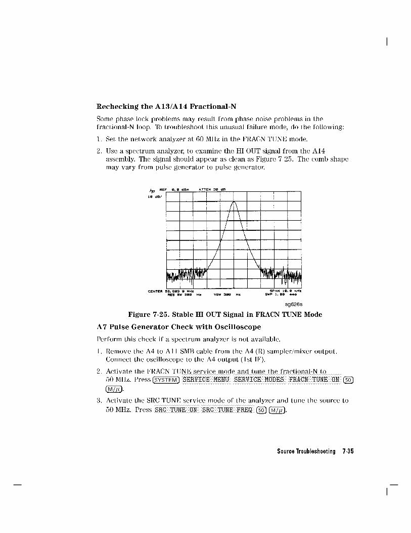
Rechecking the A13/A14 Fractional-N
Some phase lock problems may result from phase noise problems in thefractional-N loop. To troubleshoot this unusual failure mode, do the following:
1. Set the network analyzer at 60 MHz in the FRACN TUNE mode.
2. Use a spectrum analyzer, to examine the HI OUT signal from the A14assembly. The signal should appear as clean as Figure 7-25. The comb shape
may vary from pulse generator to pulse generator.
Figure 7-25. Stable HI OUT Signal in FRACN TUNE Mode
A7 Pulse Generator Check with Oscilloscope
Perform this check if a spectrum analyzer is not available.
1. Remove the A4-to-A11 SMB cable from the A4 (R) sampler/mixer output.Connect the oscilloscope to the A4 output (1st IF).
2. Activate the FRACN TUNE service mode and tune the fractional-N to
50 MHz. Press �SYSTEM�NNNNNNNNNNNNNNNNNNNNNNNNNNNNNNNNNNNNNNSERVICE MENU
NNNNNNNNNNNNNNNNNNNNNNNNNNNNNNNNNNNNNNNNNSERVICE MODES
NNNNNNNNNNNNNNNNNNNNNNNNNNNNNNNNNNNNNNNNNFRACN TUNE ON �50�
�M/��.
3. Activate the SRC TUNE service mode of the analyzer and tune the source to
50 MHz. PressNNNNNNNNNNNNNNNNNNNNNNNNNNNNNNNNNNNSRC TUNE ON
NNNNNNNNNNNNNNNNNNNNNNNNNNNNNNNNNNNNNNNNNSRC TUNE FREQ �50� �M/��.
Source Troubleshooting 7-35

4. Set the SRC TUNE frequency to those listed in Table 7-7 and observe the 1stIF waveforms. They should appear similar to Figure 7-26.
If the signals observed are correct, continue with \A11 Phase Lock Check."
If the signals observed are questionable, use a spectrum analyzer toperform the preceding \A7 Pulse Generator Check with SpectrumAnalyzer."
Table 7-7. 1st IF Waveform Settings
SRC TUNE FRACN Harmonic 1st IF
50 MHz 50 MHz 1 1 to 6 MHz
250 MHz 50 MHz 5 1 to 6 MHz
2550 MHz 50 MHz 51 1 to 6 MHz
Figure 7-26. Typical 1st IF Waveform in FRACN TUNE/SRC TUNE Mode
7-36 Source Troubleshooting

A11 Phase Lock Check
At this point, the A11 phase lock assembly appears to be faulty (its inputsshould have been veri�ed already). Nevertheless, you may elect to use thephase lock diagnostic routines or check the relevant signals at the assemblyitself for con�rmation.
Note If external source mode is the only operating mode with phaselock problems, replace the A11 phase lock assembly.
Phase Lock Check with PLL DIAG
Refer to \Phase Lock Diagnostic Tools" in \Source Group Troubleshooting
Appendix" at the end of this chapter for an explanation of the error messages
and the diagnostic routines. Follow the steps there to determine in which state
the phase lock is lost.
If NO IF FOUND is displayed, con�rm that the analog bus is functional andperform the \Source Pretune Correction Constants (Test 48)" as outlined in
the \Adjustments and Correction Constants" chapter.
If phase lock is lost in the ACQUIRE state, the A11 assembly is faulty.
If phase lock is lost in the TRACK state, troubleshoot source phase lock loop
components other than the A11 assembly.
Phase Lock Check by Signal Examination
To con�rm that the A11 assembly is receiving the signals required for its
operation, perform the following steps.
1. Place the A11 assembly on the large extender board.
2. Switch on the analyzer and press �PRESET�.
3. Check for the signals listed in Table 7-8.
Source Troubleshooting 7-37

Table 7-8. A11 Input Signals
Mnemonic I/O Access See
Figure
Notes
FM COIL � O A11P1-3,33 Figure 7-27 Aids YO COIL in setting YIG. Press �PRESET� �MENU�??????????????????????????????????????????NUMBER OF POINTS �3� ��1� to observe this signal.
REF I A11TP9 Figure 7-9,
Figure 7-10
Observe both low band and high band CW frequencies.
YO COIL + O A11P1-2,32 Figure 7-7 Use????????????????????????????????????SOURCE PLL OFF .
YO COIL � O A11P1-1,31 Figure 7-7
1ST IF I A11 PL IF IN Figure 7-26 Check for 1 MHz with tee a A11 jack (not at cable end) in
high band.
Figure 7-27. FM Coil { Plot with 3 Point Sweep
4. If any of the input signal is not correct, refer to the overall block diagram inthe \Start Troubleshooting Here"chapter as an aid to trouble shooting theproblem to its source.
5. If any of the output signals are incorrect, the A11 assembly is faulty.
7-38 Source Troubleshooting

Source Group Troubleshooting Appendix
Troubleshooting Source Problems with the Analog Bus
The analog bus can perform a variety of fast checks. However, it too is subjectto failure and should be tested prior to use. You should have done this in the\Start Troubleshooting Here" chapter.
To use the analog bus to check any one of the nodes, press �PRESET� �SYSTEM�NNNNNNNNNNNNNNNNNNNNNNNNNNNNNNNNNNNNNNSERVICE MENU
NNNNNNNNNNNNNNNNNNNNNNNNNNNNNNNNNNNNNNNNNANALOG BUS ON . Then press �MEAS�
NNNNNNNNNNNNNNNNNNNNNNNNNNNNNNNNNNNNNNNNNNNNNNNNNNNNNNNNNNNANALOG IN Aux Input
and enter the analog bus node number followed by ��1�. Refer to \AnalogBus" in the \Service Key Menus and Error Messages" chapter for additionalinformation.
Phase Lock Diagnostic Tools
error messages
diagnostic routines
Phase Lock Error Messages
All phase lock error messages can result from improper front panel connections.
NO IF FOUND: CHECK R INPUT LEVEL means no IF was detected during pretune:
a source problem. Perform the \A4 Sampler/Mixer Check."
NO PHASE LOCK: CHECK R INPUT LEVEL means the IF was not acquired after
pretune: a source problem. Perform the \A4 Sampler/Mixer Check," earlier inthis chapter.
PHASE LOCK CAL FAILED means that a calculation of pretune values was notsuccessful: a source or receiver failure. Perform the \Source Pretune CorrectionConstants" routine as outlined in the \Adjustments and Correction Constants"chapter. If the analyzer fails that routine, perform the \A4 Sampler/MixerCheck."
PHASE LOCK LOST means that phase lock was lost or interrupted before the band
sweep ended: a source problem. Refer to \Phase Lock Diagnostic Routines"
next to access the phase lock loop diagnostic service routine. Then troubleshoot
the problem by following the procedures in this chapter.
Source Troubleshooting 7-39

Phase Lock Diagnostic Routines
Perform the following steps to determine at what frequencies and bands thephase lock problem occurs.
1. Press �PRESET� �SYSTEM�NNNNNNNNNNNNNNNNNNNNNNNNNNNNNNNNNNNNNNSERVICE MENU
NNNNNNNNNNNNNNNNNNNNNNNNNNNNNNNNNNNNNNNNNSERVICE MODES
NNNNNNNNNNNNNNNNNNNNNNNNNNNNNNNNNNNNNNPLL AUTO OFF to
switch o� the automatic phase-locked loop. Normally, when the phase-lockedloop detects lock problems, it automatically aborts the sweep and attempts torecalibrate the pretune cycle. Switching o� PLL AUTO defeats this routine.
2. PressNNNNNNNNNNNNNNNNNNNNNNNNNNNNNNNNNNNPLL DIAG ON to switch on the phase-locked loop diagnostic service
mode. In this mode, the phase lock cycle and subsweep number are displayedon the analyzer display. (See \Service modes menu" in the \Service KeyMenus and Error Messages" chapter for more information.)
3. PressNNNNNNNNNNNNNNNNNNNNNNNNNNNNNPLL PAUSE to pause the phase lock sequence and determine where the
source is trying to tune when lock is lost.
Refer to \Source theory" in the \Theory of Operation" chapter for additionalinformation regarding band related problems. Then use the procedures in this
chapter to check source functions at speci�c frequencies.
Broadband Power Problems
This section assumes that a power problem exists across the full frequencyrange, but that no error message is displayed on the analyzer. The problem will
only e�ect the re ection test port. Assemblies in question include:
A3 source
A30 dual directional coupler
any cables from the A3 source to the output of the re ection test port
7-40 Source Troubleshooting
8
Receiver Troubleshooting
Use this procedure only if you have read the \Start Troubleshooting Here"chapter. Follow the procedures in the order given, unless instructed otherwise.
The receiver group assemblies consist of the following:
A4/5/6 sampler/mixer assemblies
A10 digital IF assembly
A30 dual directional coupler
Receiver Troubleshooting 8-1

Assembly Replacement Sequence
The following steps show the sequence to replace an assembly in an HP 8752CNetwork Analyzer.
1. Identify the faulty group. Refer to the \Start Troubleshooting Here" chapter.Follow up with the appropriate troubleshooting chapter that identi�es thefaulty assembly.
2. Order a replacement assembly. Refer to the \Replaceable Parts" chapter.
3. Replace the faulty assembly and determine what adjustments are necessary.Refer to the \Assembly Replacement and Post-Repair Procedures" chapter.
4. Perform the necessary adjustments. Refer to the \Adjustments and
Correction Constants" chapter.
5. Perform the necessary performance tests. Refer to the \System Veri�cationand Performance Tests" chapter.
Receiver Failure Error Messages
There are two error messages that indicate receiver group problems. Thesemessages may be caused by the analyzer itself or by external devices orconnections. An explanation of each error message follows.
CAUTION: OVERLOAD ON REFL PORT, POWER REDUCED
You have exceeded approximately +20 dBm at the re ection port. The RFoutput power is automatically reduced to � 20 dBm. The annotation P #appears in the left margin of the display to indicate that the power trip functionhas been activated.
To reset the analyzer's power and regain control of the power level, do the
following:
1. Remove any devices under test which may have contributed excess power tothe analyzer's re ection port.
2. Press �MENU�NNNNNNNNNNNNNNNNNPOWER �0� ��1�
NNNNNNNNNNNNNNNNNNNNNNNNNNNNNNNNNNNNNNNNNNNNNNNSOURCE POWER ON to turn the analyzer's
internal source back on.
8-2 Receiver Troubleshooting

If the power trip indicator (P#) does not reappear, recon�gure the testsetup to keep input power levels at 0 dBm or below.
If P# reappears, continue with \Check the R, A, and B Inputs."
CAUTION: OVERLOAD ON TRANS PORT, POWER REDUCED
You have exceeded approximately +4 dBm at the transmission port. TheRF output power is automatically reduced to � 20 dBm. The annotation P #appears in the left margin of the display to indicate that the power trip functionhas been activated.
To reset the analyzer's power and regain control of the power level, do thefollowing:
1. Remove any devices under test which may have contributed excess power tothe analyzer's transmission port.
2. Connect a cable from the re ection port to the transmission port.
3. Press �MENU�NNNNNNNNNNNNNNNNNPOWER �0� ��1�
NNNNNNNNNNNNNNNNNNNNNNNNNNNNNNNNNNNNNNNNNNNNNNNSOURCE POWER ON to turn the analyzer's
internal source back on.
If the power trip indicator (P#) does not reappear, recon�gure the testsetup to keep input power levels at 0 dBm or below.
If P# reappears, continue with \Check the R, A, and B Inputs."
Receiver Troubleshooting 8-3

Check the R, A, and B Inputs
Use the following procedure to check the atness of the R, A, and B inputtraces by comparing them with the sample traces shown in Figure 8-1 throughFigure 8-3.
1. Check the R trace
a. Press �MEAS�NNNNNNNNNNNNNNNNNNNNNNNNNNNNNNNNNNNINPUT PORTS
NNNNNR �SCALE REF�
NNNNNNNNNNNNNNNNNNNNNNNNNNNNNNNNAUTO SCALE .
b. Check the atness of the R trace by comparing it with the trace inFigure 8-1.
Figure 8-1. Sample R Input Trace
2. Check the A trace.
a. Connect a short to the re ection test port of the analyzer.
b. Press �MEAS�NNNNNNNNNNNNNNNNNNNNNNNNNNNNNNNNNNNINPUT PORTS
NNNNNA �SCALE REF�
NNNNNNNNNNNNNNNNNNNNNNNNNNNNNNNNAUTO SCALE .
c. Check the atness of the input A trace by comparing it with the trace inFigure 8-2.
8-4 Receiver Troubleshooting
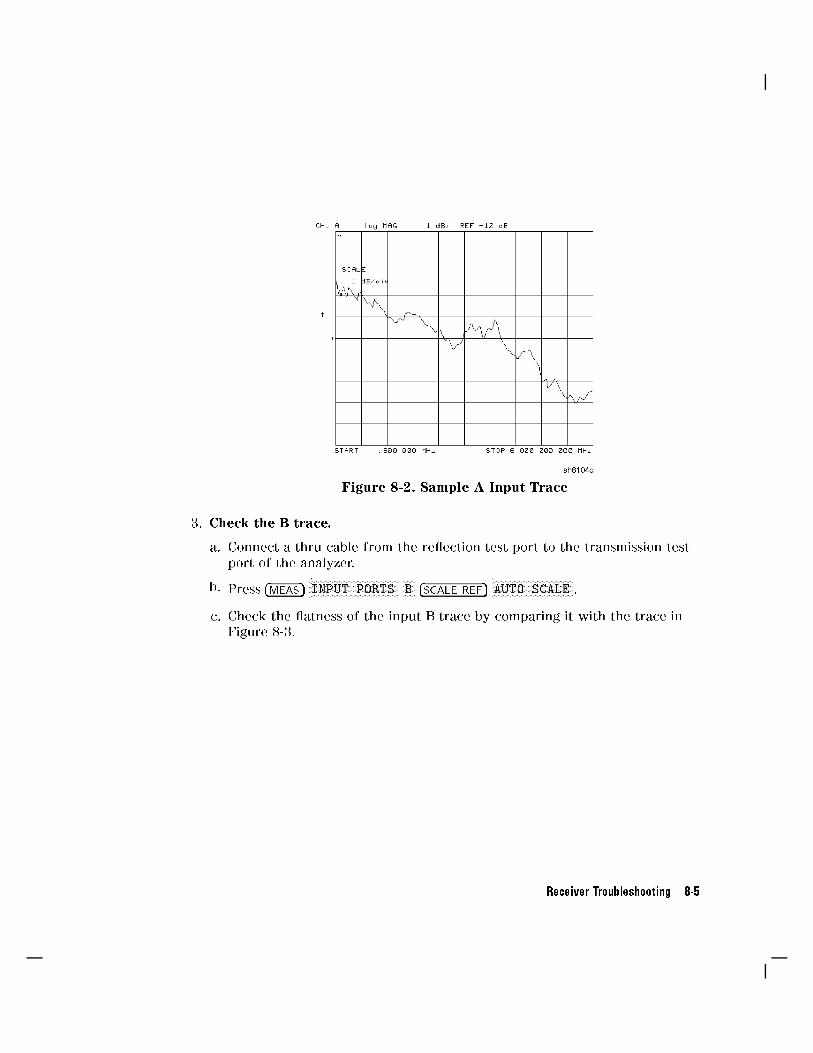
Figure 8-2. Sample A Input Trace
3. Check the B trace.
a. Connect a thru cable from the re ection test port to the transmission testport of the analyzer.
b. Press �MEAS�NNNNNNNNNNNNNNNNNNNNNNNNNNNNNNNNNNNINPUT PORTS
NNNNNB �SCALE REF�
NNNNNNNNNNNNNNNNNNNNNNNNNNNNNNNNAUTO SCALE .
c. Check the atness of the input B trace by comparing it with the trace inFigure 8-3.
Receiver Troubleshooting 8-5

Figure 8-3. Sample B Input Trace
4. Review the results.
If none of the input traces resemble the corresponding sample trace,
continue with \Troubleshooting When All Inp;uts Look Bad."
If at least one input trace resembles its corresponding sample trace,continue with \Troubleshooting When One or More Inputs Look Good."
8-6 Receiver Troubleshooting

Troubleshooting When All Inputs Look Bad
Run Internal Tests 18 and 17
1. Press �PRESET� �SYSTEM�NNNNNNNNNNNNNNNNNNNNNNNNNNNNNNNNNNNNNNSERVICE MENU
NNNNNNNNNNNNNNNNNTESTS �18� ��1�
NNNNNNNNNNNNNNNNNNNNNNNNNNNNNNNNNNNNNNEXECUTE TEST to
run the ADC o�set.
2. Then, when the analyzer �nishes test 18, press �17� ��1�NNNNNNNNNNNNNNNNNNNNNNNNNNNNNNNNNNNNNNEXECUTE TEST to
run the ADC linearity test.
3. If either of these tests FAIL, continue with \Check the 4 MHz REF Signal."
Receiver Troubleshooting 8-7

Check the 4 MHz REF Signal
1. Press �PRESET�.
2. Use an oscilloscope to observe the 4 MHz reference signal at A10P2-6.
If the signal does not resemble Figure 8-4, troubleshoot the signal source(A12P2-36) and path.
If the signal is good, the probability is greater than 90% that the A10assembly is faulty. For con�rmation, perform \Vhrvk S10 by Substitutionor Signal Examination.."
Figure 8-4. 4 MHz REF Waveform
Check A10 by Substitution or Signal Examination
If the 4 MHz REF signal is good at the A10 digital IF assembly, check the A10assembly by one of the following methods:
Substitute another A10 assembly and rerun internal tests 18 and 17.
Check the signal/control lines required for its operation. The pins and signalsources of those lines are identi�ed in Table 8-1. It is possible that the A9
assembly may not be providing the necessary signals. These signal checks
allow you to determine which assembly is faulty. Some of the waveforms areillustrated by Figure 8-5 and Figure 8-6.
8-8 Receiver Troubleshooting

If the substitute assembly shows no improvement or if all of the input signalsare valid, continue with \Check the 4 kHz Signal." Otherwise troubleshoot thesuspect signal(s) or consider the A10 assembly faulty.
Table 8-1. Signals Required for A10 Assembly Operation
Mnemonic Description A10
Location
Signal
Source
See
Figure
DIFD0 Digital IF data 0 (LSB) P2-27 A9P2-27 *
DIFD1 Digital IF data 1 P2-57 A9P2-57 *
DIFD2 Digital IF data 2 P2-28 A9P2-28 *
DIFD3 Digital IF data 3 P2-58 A9P2-58 *
DIFD4 Digital IF data 4 P2-29 A9P2-29 *
DIFD5 Digital IF data 5 P2-59 A9P2-59 *
DIFD6 Digital IF data 6 P2-30 A9P2-30 *
DIFD7 Digital IF data 7 (MSB) P2-60 A9P2-60 *
L DIFEN0 Digital IF enable 0 P2-34 A9P2-34 *
L DIFEN1 Digital IF enable 1 P2-5 A9P2-5 *
L DIFEN2 Digital IF enable 2 P2-35 A9P2-35 *
DIFCC Digital IF conversion comp. P2-33 A10P2-33 Figure 8-5
DIFCLK Digital IF serial clock P2-4 A10P2-4 Figure 8-5
DIF DATA Digital IF serial data out P2-3 A10P2-3 Figure 8-5
L ENDIF L=enable digital IF P2-17 A9P2-17 Figure 8-6
L INTCOP L=interrupt, DSP P2-2 A10P2-2 Figure 8-6
*Check for TTL activity.
Receiver Troubleshooting 8-9

Figure 8-5. Digital Data Lines Observed Using L INTCOP as Trigger
Figure 8-6. Digital Control Lines Observed Using L INTCOP as Trigger
8-10 Receiver Troubleshooting

Troubleshooting When One or More Inputs Look Good
Since at least one input is good, all of the common receiver circuitry beyond themultiplexer is functional. Only the status of the individual sampler/mixers andtheir individual signal paths is undetermined.
If all inputs look good but the average power level is incorrect, continue with\Check the Frequency Response Correction."
If one or two inputs look bad, continue with \Check the 4 kHz Signal."
Check the Frequency Response Correction
1. Remove all connections to the re ection and transmission ports and press�PRESET�. You should observe a straight line at 0 dB with a scale of 5 dB/DIV.
2. Connect a thru between the re ection and transmission ports. Press �CH 2�.The trace observed should be the same as the previous one.
If the traces are not as described, perform the Frequency ResponseCorrection adjustment in the \Adjustments and Correction Constants"
chapter.
If the traces are still not as described after performing the adjustment,replace the A10 assembly.
Check the 4 kHz Signal
1. Press �PRESET� �MENU�NNNNNNNNNNNNNNNNNNNNNNNCW FREQ .
2. Use an oscilloscope to check the 4 kHz output of the sampler/mixer inquestion at the A10 assembly. The input and output access pins are listed inTable 8-2. The signal should resemble the waveform of Figure 8-7.
If the signal is good, replace the A10 assembly.
If the signal is bad, continue with \Check 1st LO Signal at Sampler/Mixer."
Receiver Troubleshooting 8-11
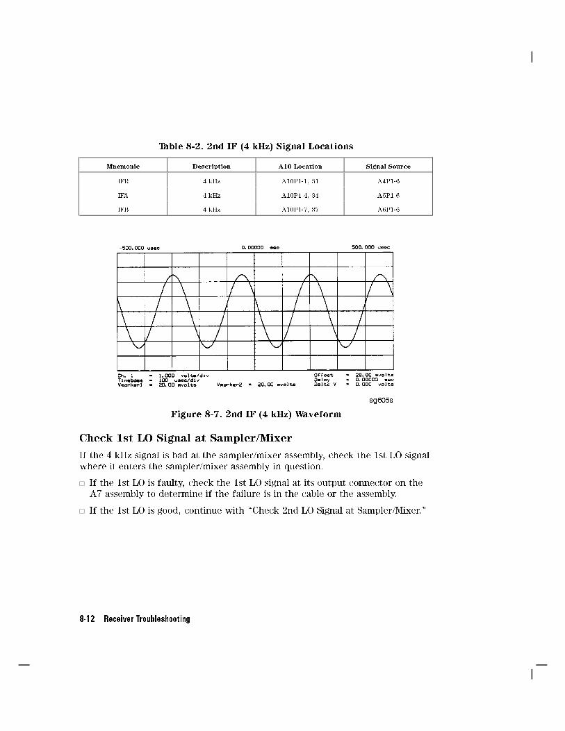
Table 8-2. 2nd IF (4 kHz) Signal Locations
Mnemonic Description A10 Location Signal Source
IFR 4 kHz A10P1-1, 31 A4P1-6
IFA 4 kHz A10P1-4, 34 A5P1-6
IFB 4 kHz A10P1-7, 37 A6P1-6
Figure 8-7. 2nd IF (4 kHz) Waveform
Check 1st LO Signal at Sampler/Mixer
If the 4 kHz signal is bad at the sampler/mixer assembly, check the 1st LO signalwhere it enters the sampler/mixer assembly in question.
If the 1st LO is faulty, check the 1st LO signal at its output connector on theA7 assembly to determine if the failure is in the cable or the assembly.
If the 1st LO is good, continue with \Check 2nd LO Signal at Sampler/Mixer."
8-12 Receiver Troubleshooting

Check 2nd LO Signal at Sampler/Mixer
Check the 2nd LO signal at the pins identi�ed in Table 8-3. Refer to the \A12Reference Check" in the \Source Troubleshooting" chapter for analog busand oscilloscope checks of the 2nd LO and waveform illustrations. Table 8-3identi�es the signal location at the samplers and the A12 assembly.
Table 8-3. 2nd LO Locations
Mnemonic Description Sampler
Location
Signal
Source
2nd LO 1 2nd LO (0 degrees) A4/5/6 P1-11 A12P1-2, 32
2nd LO 2 2nd LO (�90 degrees) A4/5/6 P1-4 A12P1-4, 34
If the 2nd LO is bad, troubleshoot the A12 reference assembly and signalpath.
If the 2nd LO is good and the B sampler is suspected faulty, replace the A6(B) sampler/mixer.
If the 2nd LO is good but the R or A sampler is suspected faulty, continue
with \Check Input Trace."
Receiver Troubleshooting 8-13

Check Input Trace
All inputs to the sampler have been veri�ed except for the signal coming fromthe coupler. The problem is most likely a faulty coupler or sampler. However,the A10 assembly may also be at fault.
Press �PRESET� �MEAS�NNNNNNNNNNNNNNNNNNNNNNNNNNNNNNNNNNNINPUT PORTS and select the input with the bad trace.
The trace normally has a number of jumps in it due to band switches, as shownin Figure 8-1 through Figure 8-3. Each jump should be less than 2 dB.
If there are other peaks or holes in the trace, the sampler is probably faulty.Remove the suspected sampler and exchange it with the known good sampler.If the problem disappears, replace the suspected sampler.
If there is a broadband problem, it is probably caused by the coupler.
If the level (average value) of the trace is wrong but the trace is otherwisecorrect, the problem is most likely in the coupler or the A10 assembly.
Either measure the output of the coupler with a power meter, or swap the
A10 assembly with another known working A10 assembly.
Check directivity, source match, and crosstalk by performing the
system veri�cation procedure described in the \System Veri�cation and
Performance Tests" chapter. If any of these fail, check the coupler and
sampler connections.
To verify the coupler is faulty, remove the sampler that has the bad input
and exchange it with the known good sampler. If there is no improvement,
replace the coupler. If the problem disappears, replace the original sampler.
If the 2nd LO is good at the sampler/mixer, the sampler/mixer assembly is faulty.
Otherwise, troubleshoot the A12 assembly and associated signal path.
8-14 Receiver Troubleshooting
9
Accessories Troubleshooting
Use this procedure only if you have read Chapter 4, \Start TroubleshootingHere." Follow the procedures in the order given, unless instructed otherwise.
Measurement failures can be divided into two categories:
Failures which don't a�ect the normal functioning of the analyzer but render
incorrect measurement data.
Failures which impede the normal functioning of the analyzer or prohibit the
use of a feature.
This chapter addresses the �rst category of failures which are usually caused bythe following:
operator errors
faulty calibration devices or connectors
bad cables or adapters
improper calibration techniques
These failures are checked using the following procedures:
\Inspect the Accessories"
\Inspect the Error Terms"
Accessories Troubleshooting 9-1

Assembly Replacement Sequence
The following steps show the sequence to replace an assembly in an HP 8752CNetwork Analyzer.
1. Identify the faulty group. Refer to the \Start Troubleshooting Here" chapter.Follow up with the appropriate troubleshooting chapter that identi�es thefaulty assembly.
2. Order a replacement assembly. Refer to the \Replaceable Parts" chapter.
3. Replace the faulty assembly and determine what adjustments are necessary.Refer to the \Assembly Replacement and Post-Repair Procedures" chapter.
4. Perform the necessary adjustments. Refer to the \Adjustments and
Correction Constants" chapter.
5. Perform the necessary performance tests. Refer to the \System Veri�cationand Performance Tests" chapter.
9-2 Accessories Troubleshooting

Inspect the Accessories
Inspect the Test Port Connectors and Calibration Devices
1. Check for damage to the mating contacts of the test port center conductorsand loose connector bulkheads.
2. Inspect the calibration kit devices for bent or broken center conductors andother physical damage. Refer to the calibration kit operating and servicemanual for information on gaging and inspecting the device connectors.
If any calibration device is obviously damaged or out of mechanicaltolerance, replace the device.
Inspect the Error Terms
Error terms are a measure of a \system": a network analyzer, calibration kit,
and any cables used. As required, refer to Chapter 11, \Error Terms", for the
following:
The speci�c measurement calibration procedure used to generate the errorterms.
The routines required to extract error terms from the instrument.
Typical error term data.
Use Table 9-1 to cross-reference error term data to system faults.
Accessories Troubleshooting 9-3

Table 9-1. Components Related to Speci�c Error Terms
Component Directivity Source
Match
Re ection
Tracking
Isolation Load
Match
Transmission
Tracking
Calibration Kit
load X
open/short X X
Analyzer
sampler X X X
A10 digital IF X
dual directional coupler X X X X X X
test port connectors X X X X X X
External cables X X
If you detect problems using error term analysis, use the following approach to
isolate the fault:
1. Check the cable by examining the load match and transmission trackingterms. If those terms are incorrect, go to \Cable Test".
2. Verify the calibration kit devices:
Loads: If the directivity error term looks good, the load and the port aregood. If directivity looks bad, check directivity again with a known goodload. If the problem is still present, replace the dual directional couplerassembly.
Shorts and opens: If the source match and re ection tracking terms lookgood, the shorts and the opens are good. If these terms look bad while therest of the terms look good, proceed to \Verify Shorts and Opens."
9-4 Accessories Troubleshooting

Cable Test
The load match error term is a good indicator of cable problems. You canfurther verify a faulty cable by measuring the re ection of the cable. Connectthe suspect cable between the re ection port and the transmission port.
Figure 9-1 shows the return loss trace of a good (left side) and faulty cable.Note that the important characteristic of a cable trace is its level (the good cabletrace is much lower) not its regularity. Refer to the cable manual for return lossspeci�cations.
Another way to verify the operation of the cable is to run the Cable Con�dence
Test (test number 22). Press �SYSTEM�NNNNNNNNNNNNNNNNNNNNNNNNNNNNNNNNNNNNNNSERVICE MENU
NNNNNNNNNNNNNNNNNTESTS �22� �x1�
NNNNNNNNNNNNNNNNNNNNNNNEXECUTE .
Figure 9-1. Typical Return Loss Traces of Good and Poor Cables
Accessories Troubleshooting 9-5

Verify Shorts and Opens
Substitute a known good short and open of the same connector type and sex asthe short and open in question. If the devices are not from one of the standardcalibration kits, refer to the HP 8752C Network Analyzer User's Guide for
information on how to use theNNNNNNNNNNNNNNNNNNNNNNNNNNNNNNNNNNNNNNNNNNNNMODIFY CAL KIT function. Set aside the short
and open that are causing the problem.
1. Perform a re ection 1-port calibration using the good short and open. Then
pressNNNNNNNNNNNNNNNNNNNNFORMAT
NNNNNNNNNNNNNNNNNNNNNNNNNNNNNNNNNNNSMITH CHART to view the devices in Smith chart format.
2. Connect the good short to the re ection port. Press �SCALE REF�NNNNNNNNNNNNNNNNNNNNNNNNNNNNNNNNNNNNNNNNNNNNNNNNNNELECTRICAL DELAY . Turn the front panel knob to enter enough electrical
delay so that the trace appears as a dot at the left side of the smith chart(see Figure 9-2a).
Replace the good short with the questionable short at the re ection port.The trace of the questionable short should appear very similar to the knowngood short.
3. Connect the good open to the re ection port. Press �SCALE REF�NNNNNNNNNNNNNNNNNNNNNNNNNNNNNNNNNNNNNNNNNNNNNNNNNNELECTRICAL DELAY and turn the front panel knob to enter enough electrical
delay so that the trace appears as a dot at the right side of the circle (seeFigure 9-2b).
Replace the good open with the questionable open at the re ection port. Thetrace of the questionable open should appear very similar to the known good
open.
9-6 Accessories Troubleshooting
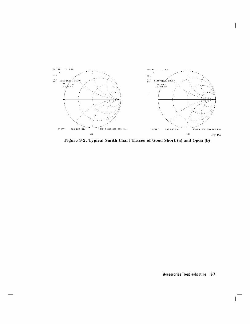
Figure 9-2. Typical Smith Chart Traces of Good Short (a) and Open (b)
Accessories Troubleshooting 9-7

10
Service Key Menus and Error Messages
Service Key Menus
These menus allow you to perform the following service functions:
testverifyadjustcontroltroubleshoot
The menus are divided into two groups:
Internal DiagnosticsService Features
When applicable, the HP-IB mnemonic is written in parentheses following the
key. See HP-IB Service Mnemonic De�nitions at the end of this section.
Error Messages
The displayed messages that pertain to service functions are also listed in thischapter to help you:
Understand the message.
Solve the problem.
Service Key Menus and Error Messages 10-1

Service Key Menus - Internal Diagnostics
The internal diagnostics menus are shown in Figure 10-1 and described in thefollowing paragraphs. The following keys access the internal diagnostics menus:
NNNNNNNNNNNNNNNNNTESTSNNNNNNNNNNNNNNNNNNNNNNNNNNNNNNNNNNNNNNTEST OPTIONSNNNNNNNNNNNNNNNNNNNNNNNNNNNNNNNNNNNNNNNNNSELF-DIAGNOSE
Figure 10-1. Internal Diagnostics Menus
Note Throughout this service guide, these conventions are observed:
�HARDKEYS� are labeled front panel keysNNNNNNNNNNNNNNNNNNNNNNNNNNSOFTKEYS are display de�ned keys (in the menus)
(HP-IB COMMANDS) when applicable, follow the keystrokesin parentheses
10-2 Service Key Menus and Error Messages

Tests Menu
To access this menu, press �SYSTEM�NNNNNNNNNNNNNNNNNNNNNNNNNNNNNNNNNNNNNNSERVICE MENU
NNNNNNNNNNNNNNNNNTESTS .
NNNNNNNNNNNNNNNNNTESTS (TEST [D]) accesses a menu that allows you to select or execute
the service tests. The default is set to internaltest 1.
Note Descriptions of tests in each of the categories are given underthe heading Test Descriptions in the following pages.
The tests are divided by function into the followingcategories:
Internal Tests (0|20)
External Tests (21|26)System Veri�cation Tests (27|43)
Adjustment Tests (44|58)
Display Tests (59|65)
Test Patterns (66|80)
To access the �rst test in each category, press thecategory softkey. To access the other tests, use the
numeric keypad, step keys or front panel knob. The
test number, name, and status abbreviation will be
displayed in the active entry area of the display.
Service Key Menus and Error Messages 10-3

Table 10-1 shows the test status abbreviation that appears on the display, itsde�nition, and the equivalent HP-IB code. The HP-IB command to outputthe test status of the most recently executed test is OUTPTESS. For moreinformation, refer to \HP-IB Service Mnemonic De�nitions" located at the endof this chapter.
Table 10-1. Test Status Terms
Display Abbreviation De�nition HP-IB Code
PASS PASS 0
FAIL FAIL 1
-IP- IN PROGRESS 2
(NA) NOT AVAILABLE 3
-ND- NOT DONE 4
DONE DONE 5
NNNNNNNNNNNNNNNNNNNNNNNNNNNNNNNNNNNNNNEXECUTE TEST (EXET) runs the selected test and may display these
softkeys:NNNNNNNNNNNNNNNNNNNNNNNNNNCONTINUE (TESR1) continues the selected test.
NNNNNNNNNNNYES (TESR2) alters correction constants during
adjustment tests.NNNNNNNNNNNNNNNEXT (TESR4) displays the next choice.
NNNNNNNNNNNNNNNNNNNNSELECT (TESR6) chooses the option indicated.
NNNNNNNNNNNNNNNNNABORT (TESR8) terminates the test and returns to
the tests menu.NNNNNNNNNNNNNNNNNNNNNNNNNNNNNNNNNNNNNNNNNNNNINTERNAL TESTS evaluates the analyzer's internal operation. These
tests are completely internal and do not requireexternal connections or user interaction.
NNNNNNNNNNNNNNNNNNNNNNNNNNNNNNNNNNNNNNNNNNNNEXTERNAL TESTS evaluate the analyzer's external operation. These
additional tests require some user interaction (suchas keystrokes).
10-4 Service Key Menus and Error Messages

NNNNNNNNNNNNNNNNNNNNNNNNNNNNNNNNNNNNNNNNNSYS VER TESTS veri�es the analyzer system operation by examining
the contents of the measurement calibration arrays.The procedure is in the \System Veri�cation andPerformance Tests" chapter. Information about thecalibration arrays is provided in the \Error Terms"chapter.
NNNNNNNNNNNNNNNNNNNNNNNNNNNNNNNNNNNNNNNNNNNNNNNNNNADJUSTMENT TESTS generates and stores the correction constants.
For more information, refer to the \Adjustments"chapter.
NNNNNNNNNNNNNNNNNNNNNNNNNNNNNNNNNNNNNNNNNDISPLAY TESTS checks for correct operation of the display and GSP
board.
Test Options Menu
To access this menu, press �SYSTEM�NNNNNNNNNNNNNNNNNNNNNNNNNNNNNNNNNNNNNNSERVICE MENU
NNNNNNNNNNNNNNNNNNNNNNNNNNNNNNNNNNNNNNTEST OPTIONS .
NNNNNNNNNNNNNNNNNNNNNNNNNNNNNNNNNNNNNNTEST OPTIONS accesses softkeys that a�ect the way tests (routines)
run, or supply necessary additional data.NNNNNNNNNNNNNNNNNNNNNNNNNNNNNNNNNNNNNNNNNCONTINUE TEST (TESR1) resumes the test from where it was stopped.
NNNNNNNNNNNNNNNNNNNNNNNNNNNNNNNNNNNNNNNNNREPEAT on OFF (TO2) toggles the repeat function on and o�. When the
function is ON, the selected test will run 10,000times unless you press any key to stop it. The
analyzer shows the current number of passes andfails.
NNNNNNNNNNNNNNNNNNNNNNNNNNNNNNNNNNNNNNNNNRECORD on OFF (TO1) toggles the record function on and o�. When the
function is ON, certain test results are sent to
a printer via HP-IB. This is especially useful forcorrection constants. The instrument must be insystem controller mode or pass control mode toprint (refer to the \Printing, Plotting, and SavingMeasurement Results" chapter in the HP 8752C
User's Guide.NNNNNNNNNNNNNNNNNNNNNNNNNNNNNNNNNNNNNNNNNNNNNNNNNNNNNLIMITS[NORM/SPCL] selects either NORMal or SPeCiaL (tighter) limits for
the Operator's Check. The SPCL limits are useful for
a guard band.NNNNNNNNNNNNNNNNNNNNNNNNNNNNNNNNPOWER LOSS (POWLLIST) accesses the following Edit List menu to allow
modi�cation of the external power loss data table.
Service Key Menus and Error Messages 10-5

NNNNNNNNNNNNNNNNNNNNNNNNNNNNNNNNNNNNNNNNNNNNNNNNNNLOSS/SENSR LISTS accesses the power loss/sensor lists menu:
NNNNNNNNNNNNNNNNNNNNNNNNNNNNNNNNNNNNNNNNNNNNUSE SENSOR A/B selects the A or B power sensor
calibration factor list for use in power metercalibration measurements.NNNNNNNNNNNNNNNNNNNNNNNNNNNNNNNNNNNNNNNNNNNNNNNNNNNNNNNNNNNCAL FACTOR SENSOR A (CALFSENA) accesses
the Edit List menu to allow modi�cation of thecalibration data table for power sensor A.NNNNNNNNNNNNNNNNNNNNNNNNNNNNNNNNNNNNNNNNNNNNNNNNNNNNNNNNNNNCAL FACTOR SENSOR B (CALFSENB) accesses
the Edit List menu to allow modi�cation of thecalibration data table for power sensor B.NNNNNNNNNNNNNNNNNNNNNNNNNNNNNNNNPOWER LOSS (POWLLIST) accesses the Edit List
menu to allow modi�cation of the external powerloss data table that corrects coupled-arm powerloss when a directional coupler samples the RFoutput.
Edit List Menu To access this menu, press �SYSTEM�NNNNNNNNNNNNNNNNNNNNNNNNNNNNNNNNNNNNNNSERVICE MENU
NNNNNNNNNNNNNNNNNNNNNNNNNNNNNNNNNNNNNNTEST OPTIONS
NNNNNNNNNNNNNNNNNNNNNNNNNNNNNNNNNNNNNNNNNNNNNNNNNNLOSS/SENSR LISTS and then press one of the following:
NNNNNNNNNNNNNNNNNNNNNNNNNNNNNNNNNNNNNNNNNNNNNNNNNNNNNNNNNNNCAL FACTOR SENSOR A or
NNNNNNNNNNNNNNNNNNNNNNNNNNNNNNNNNNNNNNNNNNNNNNNNNNNNNNNNNNNCAL FACTOR SENSOR B or
NNNNNNNNNNNNNNNNNNNNNNNNNNNNNNNNPOWER LOSS .
NNNNNNNNNNNNNNNNNNNNNNNSEGMENT selects a segment (frequency point) to be edited,
deleted from, or added to the current data table.
Works with the entry controls.NNNNNNNNNNNNNNEDIT (SEDI[D]) allows modi�cation of frequency, cal factor or loss
values previously entered in the current data table.NNNNNNNNNNNNNNNNNNNNDELETE (SDEL) deletes frequency, cal factor or loss values
previously entered in the current data table.NNNNNNNNNNNADD (SADD) adds new frequency, cal factor or loss values to the
current data table up to a maximum of 12 segments(frequency points).
NNNNNNNNNNNNNNNNNNNNNNNNNNNNNNNNCLEAR LIST (CLEL) deletes the entire current data table (or list) whenNNNNNNNNNNN
YES is pressed. PressNNNNNNNNNO to avoid deletion.
NNNNNNNNNNNNNNDONE (EDITDONE) returns to the previous menu.
10-6 Service Key Menus and Error Messages

Self Diagnose Softkey
You can access the self diagnosis function by pressing, �SYSTEM�NNNNNNNNNNNNNNNNNNNNNNNNNNNNNNNNNNNNNNSERVICE MENU
NNNNNNNNNNNNNNNNNNNNNNNNNNNNNNNNNNNNNNNNNSELF DIAGNOSE . This function examines, in order, the pass/fail status of all
internal tests and displays NO FAIL FOUND if no tests have failed.
If a failure is detected, the routine displays the assembly or assemblies mostprobably faulty and assigns a failure probability factor to each assembly.
Test Descriptions
The analyzer has up to 80 routines that test, verify, and adjust the instrument.This section describes those tests.
Internal Tests
This group of tests runs without external connections or operator interaction.All return a PASS or FAIL condition. All of these tests run on power-up and
PRESET except as noted.
0 ALL INT. Runs only when selected. It consists of internal tests 3-11,13-16, and 20. Use the front panel knob to scroll through the tests andsee which failed. If all pass, the test displays a PASS status. Each test
in the subset retains its own test status.
1 PRESET. Runs the following subset of internal tests: �rst, the
ROM/RAM tests 2, 3, and 4; then tests 5 through 11, 14, 15, and 16. Ifany of these tests fail, this test returns a FAIL status. Use the front
panel knob to scroll through the tests and see which failed. If all pass,
this test displays a PASS status. Each test in the subset retains its owntest status. This same subset is available over HP-IB as \TST?". Referto HP-IB service mnuemonics de�nitions. It is not performed uponremote preset.
2 ROM. Part of the ROM/RAM tests and cannot be run separately. Refer
to the \Digital Control Troubleshooting" chapter for more information.
3 CMOS RAM. Veri�es the A9 CPU CMOS (long-term) memory with a
non-destructive write/read pattern. A destructive version that writesover stored data is shown in Table 10-2.
Service Key Menus and Error Messages 10-7

4 Main DRAM. Veri�es the A9 CPU main memory (DRAM) with anon-destructive write/read test pattern. A destructive version is shownin Table 10-2. These tests, internal tests 2 through 4, are normally runat preset and power-on. However, a jumper on the A9 CPU assembly,illustrated in Figure 10-2, can be set in one of �ve positions with thefollowing results:
Table 10-2. Descriptions of Jumper Positions
Jumper
Position
Position
No
Result
ALTER 1 With the jumper in this right position, correction constants can
be altered, (updated) during adjustment procedures. The altered
correction constants are stored in EEPROM, replacing previously
stored correction constants.
CMOS 2 This destructive version of the CMOS RAM test (internal test 3)
continuously writes over information stored there.
DRAM 3 This destructive version of the main DRAM test (internal test 4)
continuously writes over information stored there.
SKIP 4 For factory use only.
NORMAL 5 The left position is the normal operation position.
10-8 Service Key Menus and Error Messages

Figure 10-2. Jumper Positions on the A9 CPU
For additional information, see Internal Tests and the \Digital ControlTroubleshooting" chapter.
5 DSP Wr/Rd. Veri�es the ability of the main processor and the
DSP (digital signal processor), both on the A9 CPU assembly, to
communicate with each other through DRAM. This also veri�es thatprograms can be loaded to the DSP, and that most of the main RAMaccess circuits operate correctly.
6 DSP RAM. Veri�es the A9 CPU RAM associated with the digital signalprocessor by using a write/read pattern.
7 DSP ALU. Veri�es the A9 CPU high-speed math processing portions ofthe digital signal processor.
8 DSP Intrpt. Tests the ability of the A9 CPU digital signal processor to
respond to interrupts from the A10 digital IF ADC.
9 DIF Control. Tests the ability of the A9 CPU main processor to
write/read to the control latches on the A10 digital IF.
Service Key Menus and Error Messages 10-9

10 DIF Counter. Tests the ability of the A9 CPU main processor towrite/read to the triple divider on the A10 CPU. It tests the A9CPU data bu�ers and A10 digital IF, the 4 MHz clock from the A12reference.
11 DSP Control. Tests the ability of the A9 CPU digital signal processor towrite to the control latches on the A10 digital IF. Feedback is veri�edby the main processor. It primarily tests the A10 digital IF, but failuresmay be caused by the A9 CPU.
12 Fr Pan Wr/Rd. Tests the ability of the A9 CPU main processor towrite/read to the front panel processor. It tests the A2 front panelinterface and processor, and A9 CPU data bu�ering and addressdecoding. (See also tests 23 and 24 below.) This runs only when
selected.
13 Rear Panel. Tests the ability of the A9 CPU main processor to
write/read to the rear panel control elements. It tests the A16 rearpanel, and A9 CPU data bu�ering and address decoding. (It does nottest the HP-IB interface; for that see the HP 8752C Network Analyzer
Programmer's Guide.) This runs only when selected or with ALL
INTERNAL (internal test #10).
14 Post Reg. Polls the status register of the A8 post-regulator, and
ags these conditions: heat sink too hot, inadequate air ow, or
post-regulated supply shutdown.
15 Frac N Cont. Tests the ability of the A9 CPU main processor to
write/read to the control element on the A14 fractional-N (digital)assembly. The control element must be functioning, and the
fractional-N VCO must be oscillating (although not necessarilyphase-locked) to pass.
16 Sweep Trig. Tests the sweep trigger (L SWP) line from the A14fractional-N to the A10 digital IF. The receiver with the sweepsynchronizes L SWP.
17 ADC Lin. It tests the linearity of the A10 digital IF ADC using the
built-in ramp generator. The test generates a histogram of the ADC
linearity, where each data point represents the relative \width" of aparticular ADC code. Ideally, all codes have the same width; di�erentwidths correspond to non-linearities.
10-10 Service Key Menus and Error Messages

18 ADC Ofs. This runs only when selected. It tests the ability of theo�set DAC, on the A10 digital IF, to apply a bias o�set to the IF signalsbefore the ADC input. This runs only when selected.
19 ABUS Test. Tests analog bus accuracy, by measuring several analog busreference voltages (all nodes from the A10 digital IF). This runs onlywhen selected.
20 FN Count. Uses the internal counter to count the A14 fractional-NVCO frequency (120 to 240 MHz) and the divided fractional-Nfrequency (100 kHz). It requires the 100 kHz signal from A12 and thecounter gate signal from A10 to pass.
Service Key Menus and Error Messages 10-11

External Tests
These tests require either external equipment and connections or operatorinteraction of some kind to run. Tests 23 and 24 are comprehensive front panelchecks, more complete than test 12, that checks the front panel keys and knobentry.
21 Port 1 Op Chk. Part of the \Operator's Check" procedure, locatedin the \Start Troubleshooting" chapter. The procedure requires the
external connection of a short to PORT 1.
22 Port 2 Op Chk. Same as 21, but tests PORT 2.
23 Fr Pan Seq. Tests the front panel knob entry and all A1 front panelkeys, as well as the front panel microprocessor on the A2 assembly. It
prompts the user to rotate the front panel knob, then press each key
in an ordered sequence. It continues to the next prompt only if thecurrent prompt is correctly satis�ed.
24 Fr Pan Diag. Similar to 23 above, but the user rotates the front panel
knob or presses the keys in any order. This test displays the command
the instrument received.
25 ADC Hist. Factory use only.
26 Source Ex. Factory use only.
10-12 Service Key Menus and Error Messages

System Veri�cation Tests
These tests apply mainly to system-level, error-corrected veri�cation andtroubleshooting. Test 27 is associated with the system veri�cation procedure,documented in the \System Veri�cation and Performance Tests" chapter. Tests32 to 34 facilitate examining the calibration coe�cient arrays (error terms)resulting from a measurement calibration; refer to the \Error Terms" chapter fordetails.
27 Sys Ver Init. Runs a series of measurements on devices contained inthe HP 85032B 50 Type-N Calibration Kit (for the HP 8752C) or theHP 85036B 75 Type-N Calibration Kit (for the HP 8752C Option 075).
28 - 31 Not used.
32-34 Cal Coef 1-12. Copies error term data from a measurement calibration
array to display memory. A measurement calibration must be completeand active. The de�nition of calibration arrays depends on the current
calibration type. After execution, the memory is automatically
displayed. Refer to the \Error Term" chapter for details.
Service Key Menus and Error Messages 10-13

Adjustment Tests
The tests without asterisks are used in the procedures located in the\Adjustments" chapter of this manual, except as noted.
44 *Source Def. Writes default correction constants for rudimentarysource power accuracy. Use this test before running test 47, below.
45 *Pretune Def. Writes default correction constants for rudimentary
phase lock pretuning accuracy. Use this test before running test 48,below.
46 ABUS Cor. Measures three �xed voltages on the ABUS, and generatesnew correction constants for ABUS amplitude accuracy in both highresolution and low resolution modes. Use this test before running
test 48, below.
47 Source Cor. Measures source output power accuracy, atness, andlinearity against an external power meter via HP-IB to generate newcorrection constants. Run tests 44, 45, 46, and 48 �rst.
48 Pretune Cor. Generates source pretune values for proper phase-locked
loop operation. Run tests 44, 45, and 46 �rst.
49 Intensity Cor. Stores the current values of the intensity adjustments
under �DISPLAY� for recall of display intensity values at power-on.
50 Disp 2 Ex. Not used in \Adjustments." Writes the \secondary test
pattern" to the display for adjustments. Press �PRESET� to exit this
routine.
51 IF Step Cor. Measures the gain of the IF ampli�ers (A and B only)
located on the A10 digital IF, to determine the correction constants forabsolute amplitude accuracy. It provides smooth dynamic accuracy andabsolute amplitude accuracy in the �30 dBm input power region.
52 ADC Ofs Cor. Measures the A10 Digital IF ADC linearitycharacteristics, using an internal ramp generator, and stores valuesfor the optimal operating region. During measurement, IF signals arecentered in the optimal region to improve low-level dynamic accuracy.
53 Sampler Cor. Measures the absolute amplitude response of theR sampler against an external power meter via HP-IB, then compares
A and B, (magnitude and phase), against R. It improves the R inputaccuracy and A/B/R tracking.
10-14 Service Key Menus and Error Messages
54 Cav Osc Cor. Calculates the frequency of the cavity oscillator and theinstrument temperature for e�ective spur avoidance.
55 Serial Cor. Stores the serial number (input by the user in the DisplayTitle menu) in EEPROM. This routine will not overwrite an existingserial number.
56 Option Cor. Stores the option keyword (required for Option 002, 006,010 or any combination).
57 *Cal Kit Def. Not used.
58 Init EEPROM. This test initializes certain EEPROM addresses to zerosand resets the display intensity correction constants to the defaultvalues. Also, the test will not alter the serial number and correction
constants for Option 002, 006, and 010.
Service Key Menus and Error Messages 10-15

Display Tests
These tests do not return a PASS/FAIL condition. All six amber front panelLEDs will turn o� if the test passes. The display will be blank; press �PRESET� toexit the test. If any of the six LEDs remain on, the test has failed.
59 Disp/cpu com. Checks to con�rm that the CPU can communicate withthe A19 GSP board. The CPU writes all zeros, all ones, and then awalking one pattern to the GSP and reads them back. If the test fails,
the CPU repeats the walking 1 pattern until �PRESET� is pressed.
60 DRAM cell. Tests the DRAM on A19 by writing a test pattern to theDRAM and then verifying that it can be read back.
61 Main VRAM. Tests the VRAM by writing all zeros to one location in
each bank and then writing all ones to one location in each bank.
Finally a walking one pattern is written to one location in each bank.
62 VRAM bank. Tests all the cells in each of the 4 VRAM banks.
63 VRAM/video. Veri�es that the GSP is able to successfully perform both
write and read shift register transfers. It also checks the video signals
LHSYNC, LVSYNC, and LBLANK to verify that they are active and
toggling.
64 RGB outputs. Con�rms that the analog video signals are correct and it
veri�es their functionality.
65 Inten DAC. Veri�es that the intensity DAC can be set both low and
high.
10-16 Service Key Menus and Error Messages
Test Patterns
Test patterns are used in the factory for display adjustments, diagnostics,and troubleshooting, but they are not used for �eld service. Test patternsare executed by entering the test number (66 through 80), then pressingNNNNNNNNNNNNNNNNNNNNNNNNNNNNNNNNNNNNNNEXECUTE TEST
NNNNNNNNNNNNNNNNNNNNNNNNNNCONTINUE . The test pattern will be displayed and the softkey
labels blanked. To exit the test pattern and return the softkey labels, presssoftkey 8 (bottom softkey). The following is a description of the test patterns.
66 Test Pat 1. Displays an all white screen for verifying the light outputof the A18 display and checks for color purity. In this, and othersolid test patterns, an extremely thin full-screen horizontal line willbe seen about 1/4 screen height from the bottom. This condition ischaracteristic of the display and does not indicate any problem.
67-69 Test Pat 2-4. Displays a red, green, and blue pattern for verifying the
color purity of the display and also the ability to independently control
each gun color. If the purity of the displayed test pattern is a problem,
it usually indicates that the face of the display needs to be de-gaussed
(de-magnetized). If the purity is bad, cycling the power a few timesmay cure the problem. If this does not work, a commercially availablede-magnetizer must be used.
70 Test Pat 5. Displays a 16-step gray scale for verifying that the palette
chip on the A19 GSP board can produce 16 di�erent amplitudes of
color (in this case, white.) This pattern is also very useful when usingan oscilloscope for troubleshooting. The staircase pattern it produceswill quickly show missing or stuck data bits.
71 Test Pat 6. Displays a 3-step gray scale pattern for adjusting the
background level (or 0 step) so that the �rst bar is not visible, and thesecond bar is just barely visible. This pattern consists of the �rst threegray scale bars of the 16-step gray scale.
72 Test Pat 7. Displays a convergence pattern for measuring the accuracyof the color convergence. It is mainly for use by the factory, since
convergence cannot be adjusted in the �eld.
73-74 Test Pat 8-9. Displays crosshatch and inverse crosshatch patterns
for testing color convergence, linearity, alignment, and high voltage
regulation, in the factory only. No �eld adjustments are possible.
Service Key Menus and Error Messages 10-17
75 Test Pat 10. Displays an H pattern for checking the focus ofthe display. Under normal conditions, this should never need tobe adjusted. However, it is possible to adjust it by accessing thefocus control adjustment at the left rear of the display. See the\Adjustments" chapter.
76 Test Pat 11. Veri�es the functionality of the pixel stretching circuitof the A19 GSP board. Under normal conditions, this pattern shouldappear all white. If a failure occurs in the pixel stretching circuit, thepattern will consist of 16 alternating white and gray vertical stripes.Suspect problems with the STRETCH line and LFIRSTPIX.
77 Test Pat 12. Displays a repeating gray scale for troubleshooting, usingan oscilloscope. It is similar to the 16 step gray scale but is repeated 32
times across the screen. Each of the 3 outputs of the video palette will
then show 32 ramps (instead of one staircase) between each horizontal
sync pulse. This pattern is used to troubleshoot the pixel processing
circuit of the A19 GSP board.
78 Test Pat 13. Displays a color rainbow pattern for showing the ability
of the A19 GSP board to display 15 colors plus white. The numbers
written below each bar indicate the tint number used to produce thatbar (0 & 100=pure red, 33=pure green, 67=pure blue).
79 Test Pat 14. Displays a character set for showing the user allthe di�erent types and sizes of characters available. Three sets
of characters are drawn in each of the three character sizes. 125
characters of each size are displayed. Characters 0 and 3 cannot bedrawn and several others are really control characters (such as carriagereturn and line feed).
80 Test Pat 15. Displays a bandwidth pattern for verifying the bandwidth
of the display. It consists of multiple alternating white and blackvertical stripes. Each stripe should be clearly visible. A limitedbandwidth would smear these lines together. This adjustment can beperformed in the factory only.
10-18 Service Key Menus and Error Messages

Service Key Menus - Service Features
The service feature menus are shown in Figure 10-3 and described in thefollowing paragraphs. The following keys access the service feature menus:
NNNNNNNNNNNNNNNNNNNNNNNNNNNNNNNNNNNNNNNNNSERVICE MODESNNNNNNNNNNNNNNNNNNNNNNNNNNNNNNNNNNNNNNNNNNNNNNNNNNNNNANALOG BUS on OFFNNNNNNNNNNNNNNNNNNNNNNNNNNNNNPEEK/POKENNNNNNNNNNNNNNNNNNNNNNNNNNNNNNNNNNNNNNNNNNNNNNNNNNNNNFIRMWARE REVISION
Figure 10-3. Service Feature Menus
Service Key Menus and Error Messages 10-19

Service Modes Menu
To access this menu, press: �SYSTEM�NNNNNNNNNNNNNNNNNNNNNNNNNNNNNNNNNNNNNNSERVICE MENU
NNNNNNNNNNNNNNNNNNNNNNNNNNNNNNNNNNNNNNNNNSERVICE MODES .
NNNNNNNNNNNNNNNNNNNNNNNNNNNNNNNNNNNNNNNNNSERVICE MODES allows you to control and monitor various circuits
for troubleshooting.NNNNNNNNNNNNNNNNNNNNNNNNNNNNNNNNNNNNNNNNNNNNNNNNNNNNNFRACN TUNE on OFF(SM1)
tests the A13 and A14 fractional-N circuits. It allowsyou to directly control and monitor the outputfrequency of the fractional-N synthesizer (10 MHz to60 MHz). Set the instrument to CW sweep mode andthen set FRACN TUNE ON.
Change frequencies with the front panel keys orknob. The output of the A14 assembly can be
checked at A14J1 HI OUT (in high band) or A14J2
LO OUT (in low band) with an oscilloscope, a
frequency counter, or a spectrum analyzer. Signaljumps and changes in shape at 20 MHz and 30 MHzwhen tuning up in frequency, and at 29.2 MHz and
15 MHz when tuning down, are due to switching
of the digital divider. This mode can be used with
the SRC TUNE mode as described in \SourceTroubleshooting" chapter.
NNNNNNNNNNNNNNNNNNNNNNNNNNNNNNNNNNNNNNNNNNNNNNNSRC ADJUST MENU accesses the functions that allow you to adjust the
source:NNNNNNNNNNNNNNNNNNNNNNNNNNNNNNNNNNNNNNNNNNNNNNNSRC TUNE on OFF tests the pretune functions
of the phase lock and source assemblies. Use
the entry controls to set test port output to any
frequency from 300 kHz to 6 GHz. When in thismode:
Set analyzer to CW frequency before pressingNNNNNNNNNNNNNNNNNNNNNNNNNNNNNNNNNNNSRC TUNE ON .
Test port output is 1 to 6 MHz above indicated(entered) frequency.
Instrument does not attempt to phase lock.
Residual FM increases.NNNNNNNNNNNNNNNNNNNNNNNNNNNNNNNNNNNNNNNNNSRC TUNE FREQ allow you to change the source
tune frequency.
10-20 Service Key Menus and Error Messages

NNNNNNNNNNNNNNNNNNNNNNNNNNNNNNNNALC ON off toggles the automatic leveling
control (ALC) on and o�.NNNNNNNNNNNNNNNNNNNNNNNNNNNNNNNNNNNNNNMAIN PWR DAC with the ALC switched on, the
main power dac controls the reference levelof the ALC loop. With the ALC switched o�,it controls the drive to the ALC modulator. Themain power DAC gets overwritten at everyinternal phase locking.NNNNNNNNNNNNNNNNNNNNNNNNNNNNNSLOPE DAC for manufacturing use only.
NNNNNNNNNNNNNNNNNNNNNNNNNNNNNNNNNNNNNNNNNNNNNNNSRC ADJUST DACS for manufacturing use only.
NNNNNNNNNNNNNNNNNNNNNNNNNNNNNNNNNNNNNNNNNNNNNNNNNNNNNHB FLTR SW on OFF for manufacturing use only.
NNNNNNNNNNNNNNNNNNNNNNNNNNNNNNNNNNNNNNNNNNNNNNNNNNNNNSOURCE PLL ON off(SM3)
With this mode switched OFF, the source stays in
the pretune mode and does not attempt to complete
the phase lock sequence. Also, all phase lock error
messages are disabled. The fractional-N circuits
and the receiver operate normally. Therefore, theinstrument sweeps, but the source is being driven by
the pretune DAC in a stair-stepped fashion.NNNNNNNNNNNNNNNNNNNNNNNNNNNNNNNNNNNNNNNNNNNNNNNPLL AUTO ON off (SM4) Automatically attempts to determine new pretune
values when the instrument encounters phase lock
problems (for example, \harmonic skip"). WithNNNNNNNNNNNNNNNNNNNNNNNNNNNNNNNNNNNNNNPLL AUTO OFF the frequencies and voltages do
not change, like when they are attempting to
determine new pretune values, so troubleshootingthe phase-locked loop circuits is more convenient.This function may also be turned o� to avoidpretune calibration errors in applications wherethere is a limited frequency response in the R(reference) channel. For example, in a high power
test application, using band limited �lters for Rchannel phase locking.
Service Key Menus and Error Messages 10-21

NNNNNNNNNNNNNNNNNNNNNNNNNNNNNNNNNNNNNNNNNNNNNNNPLL DIAG on OFF (SM5) displays a phase lock sequence at the beginning of
each band. This sequence normally occurs veryrapidly, making it di�cult to troubleshoot phase lockproblems. Switching this mode ON slows the processdown, allowing you to inspect the steps of the phaselock sequence (pretune, acquire, and track) bypausing at each step. The steps are indicated on thedisplay, along with the channel (C1 or C2) and bandnumber (B1 through B13).
This mode can be used with PLL PAUSE to halt theprocess at any step. It can also be used with theanalog bus counter.
NNNNNNNNNNNNNNNNNNNNNNNNNNNNNPLL PAUSE used only with PLL DIAG mode.
NNNNNNNNNNNNNNCONT indicates
that it will continuously cycle through all steps of
the phase lock sequence.NNNNNNNNNNNNNNNNNPAUSE holds it at any step
of interest. This mode is useful for troubleshootingphase-locked loop problems.
NNNNNNNNNNNNNNMORE Accesses the service modes more menu listed below.
10-22 Service Key Menus and Error Messages

Service Modes More Menu
To access this menu, press �SYSTEM�NNNNNNNNNNNNNNNNNNNNNNNNNNNNNNNNNNNNNNSERVICE MENU
NNNNNNNNNNNNNNNNNNNNNNNNNNNNNNNNNNNNNNNNNSERVICE MODES
NNNNNNNNNNNNNNMORE .
NNNNNNNNNNNNNNNNNNNNNNNNNNNNNNNNNNNNNNNNNNNNNNNNNNNNNNNNSAMPLER COR ON off(SM6)
Toggles the sampler correction routine ON,for normal operation, or OFF, for diagnosis oradjustment purposes.
NNNNNNNNNNNNNNNNNNNNNNNNNNNNNNNNNNNNNNIF GAIN AUTO Normal operating condition and works in
conjunction with IF GAIN ON and OFF. The A10assembly includes a switchable attenuator sectionand an ampli�er that ampli�es low-level 4 kHzIF signals (for A and B inputs only). This modeallows the A10 IF section to automatically determineif the attenuator should be switched in or out.The switch occurs when the A or B input signal isapproximately �30 dBm.
NNNNNNNNNNNNNNNNNNNNNNNNNNNNNNNNIF GAIN ON Locks out the A10 IF attenuator sections for
checking the A10 IF gain ampli�er circuits,
regardless of the amplitude of the A or B IF signal.
Switches out both the A and B attenuation circuits;
they cannot be switched independently. Be awarethat input signal levels above �30 dBm at the
sampler input will saturate the ADC and cause
measurement errors.NNNNNNNNNNNNNNNNNNNNNNNNNNNNNNNNNNNIF GAIN OFF Switches in both of the A10 IF attenuators for
checking the A10 IF gain ampli�er circuits. Smallinput signals will appear noisy, and raise theapparent noise oor of the instrument.
NNNNNNNNNNNNNNNNNNNNNNNNNNNNNNNNNNNNNNNNNNNNNNNNNNSPUR TEST on OFF (SM7) For factory use only.
Service Key Menus and Error Messages 10-23

NNNNNNNNNNNNNNNNNNNNNNNNNNNNNNNNNNNNNNNNNNNNNNNNNNNNNSTORE EEPR on OFF Allows you to store the correction constants that
reside in non-volatile memory (EEPROM) onto adisk. Correction constants improve instrumentperformance by compensating for speci�c operatingvariations due to hardware limitations (refer to the\Adjustments" chapter). Having this information ondisk is useful as a backup, in case the constants arelost (due to a CPU board failure). Without a diskbackup the correction constants can be regeneratedmanually, although the procedures are more timeconsuming.
NNNNNNNNNNNNNNNNNNNNNNNNNNNNNNNNNNNNNNNNNNNNNNNNNNNNNSPUR AVOID ON off(SM8)
O�sets the frequency of both the A3 YIG oscillatorand the A3 cavity oscillator to avoid spurs which
cannot otherwise be �ltered out.NNNNNNNNNNNNNNNNNNNNNNNNNNNNNNNNNNNNNNNNNNNNSPUR AVOID OFF
allows examination of these spurs for service.NNNNNNNNNNNNNNNNNNNNNNNNNNNNNNNNNNNNNNNNNNNNNNNNNNNNNANALOG BUS on OFF(ANAB)
enables and disables the analog bus, described
below. Use it with the analog in menu, (adescription of this menu follows).
10-24 Service Key Menus and Error Messages

Analog Bus
To access the analog bus, press �SYSTEM�NNNNNNNNNNNNNNNNNNNNNNNNNNNNNNNNNNNNNNSERVICE MENU
NNNNNNNNNNNNNNNNNNNNNNNNNNNNNNNNNNNNNNNNNANALOG BUS ON .
Description of the Analog Bus
The analog bus is a single multiplexed line that networks 31 nodes within theinstrument. It can be controlled from the front panel, or through HP-IB, tomake voltage and frequency measurements just like a voltmeter, oscilloscope, orfrequency counter. The next few paragraphs provide general information aboutthe structure and operation of the analog bus. See \Analog Bus Nodes," below,for a description of each individual node. Refer to the \Overall Block Diagram,"in the \Start Troubleshooting" chapter, to see where the nodes are located in
the instrument.
The analog bus consists of a source section and a receiver section. The sourcecan be the following:
any one of the 31 nodes described in \Analog Bus Nodes"the A14 fractional-N VCOthe A14 fractional-N VCO divided down to 100 kHz
The receiver portion can be the following:
the main ADCthe frequency counter
When analog bus traces are displayed, frequency is the x-axis. For a linear
x-axis in time, switch to CW time mode (or sweep a single band).
The Main ADC
The main ADC is located on the A10 digital IF assembly and makes voltage
measurements in two ranges. See \NNNNNNNNNNNNNNNNNNNNNNNNNNNNNNNNRESOLUTION ," under \Analog In Menu."
The Frequency Counter
The frequency counter is located on the A14 assembly and can count one ofthree sources:
selected analog bus node
A14 fractional-N VCO (FRAC N)
A14 fractional-N VCO divided down to 100 kHz (DIV FRAC N) (frequency
range is 100 kHz to 16 MHz)
Service Key Menus and Error Messages 10-25

The counts are triggered by the phase lock cycle; one at each pretune, acquire,and track for each bandswitch. (The service mode, SOURCE PLL, must be ONfor the counter to be updated at each bandswitch). The counter works in swept
modes or in CW mode. It can be used in conjunction withNNNNNNNNNNNNNNNNNNNNNNNNNNNNNNNNNNNNNNNNNSERVICE MODES for
troubleshooting phase lock and source problems.
To read the counter over HP-IB, use the command OUTPCNTR.
Notes
The display and marker units (U) correspond to volts.Nodes 17 (1st IF) and 24 (2nd LO) are unreliable above 1 MHz.About 0.750 MHz is a typical counter reading with no AC signal present.Anything occurring during bandswitches is not visible.Fast-moving waveforms may be sensitive to sweep time.
The analog bus input impedance is about 50K ohms.
Waveforms up to approximately 200 Hz can be reproduced.
10-26 Service Key Menus and Error Messages

Analog In Menu
Select this menu to monitor voltage and frequency nodes, using the analog busand internal counter, as explained below.
To switch on the analog bus and access the analog in menu, press:
�SYSTEM�NNNNNNNNNNNNNNNNNNNNNNNNNNNNNNNNNNNNNNSERVICE MENU
NNNNNNNNNNNNNNNNNNNNNNNNNNNNNNNNNNNNNNNNNANALOG BUS ON �MEAS�
NNNNNNNNNNNNNNNNNNNNNNNNNNNNNANALOG IN
TheNNNNNNNNNNNNNNNNNNNNNNNNNNNNNNNNNNNNNNNNNNNNNNNNNNRESOLUTION [LOW] key toggles between low and high resolution.
Resolution Maximum Signal Minimum Signal
LOW +0.5 V �0.5 V
HIGH +10 V �10 V
NNNNNNNNNNNNNNNNNNNNNNNNNNNNNNNNNNNNNNNNNNNNAUX OUT on OFF allows you to monitor the analog bus nodes (except nodes
1, 2, 3, 4, 9, 10, 12) with external equipment (oscilloscope,
voltmeter, etc.). To do this, connect the equipment to the
AUX INPUT BNC connector on the rear panel, and pressNNNNNNNNNNNNNNNNNNNNNNNAUX OUT , until
NNNNNNNNON is highlighted.
Caution To prevent damage to the analyzer, �rst connect the signal tothe rear panel AUX INPUT, and then switch the function ON.
NNNNNNNNNNNNNNNNNNNNNNNNNNNNNNNNNNNNNNCOUNTER: OFF switches the internal counter o� and removes the counter
display from the display. The counter can be switched onwith one of the next three keys. (Note: Using the counterslows the sweep.) The counter bandwidth is 16 MHz unlessotherwise noted for a speci�c node.
Note OUTPCNTR is the HP-IB command to output the counter'sfrequency data.
Service Key Menus and Error Messages 10-27

NNNNNNNNNNNNNNNNNNNNNNNNNNNNNNNNANALOG BUS switches the counter to monitor the analog bus.
NNNNNNNNNNNNNNNNNNNNFRAC N switches the counter to monitor the A14 fractional-N
VCO frequency at the node shown on the \Overall BlockDiagram," in the \Start Troubleshooting" chapter.
NNNNNNNNNNNNNNNNNNNNNNNNNNNNNNNNDIV FRAC N switches the counter to monitor the A14 fractional-N VCO
frequency after it has been divided down to 100 kHz forphase locking the VCO.
10-28 Service Key Menus and Error Messages

Analog Bus Nodes
The following paragraphs describe the 31 analog bus nodes. The nodes are listedin numerical order and are grouped by assembly. Refer to the \Overall BlockDiagram" for node locations.
A3 Source
To observe six of the eight A3 analog bus nodes (not node 5 or 8), performStep A3 to set up a power sweep on the analog bus. Then follow the node
speci�c instructions.
Step A3.Press:�PRESET�
�SYSTEM�NNNNNNNNNNNNNNNNNNNNNNNNNNNNNNNNNNNNNNSERVICE MENU
NNNNNNNNNNNNNNNNNNNNNNNNNNNNNNNNNNNNNNNNNANALOG BUS ON
�MEAS�NNNNNNNNNNNNNNNNNNNNNNNNNNNNNANALOG IN
�MENU�NNNNNNNNNNNNNNNNNNNNNNNCW FREQ �1� �.� �3� �G/n�
NNNNNNNNNNNNNNNNNNNNNNNNNNNNNNNNNNNNNNNNNNNNNNNSWEEP TYPE MENU
NNNNNNNNNNNNNNNNNNNNNNNNNNNNNNNNNNNPOWER SWEEP
Service Key Menus and Error Messages 10-29

Node 1 Mn Pwr DAC (main power DAC)
Perform step A3, above, to set up a power sweep on the analog bus. Then press
�MEAS�NNNNNNNNNNNNNNNNNNNNNNNNNNNNNANALOG IN �1� �x1� �SCALE REF�
NNNNNNNNNNNNNNNNNNNNNNNNNNNNNNNNAUTO SCALE �MKR�.
Node 1 is the output of the main power DAC. It sets the reference voltage to theALC loop. At normal operation, this node should read approximately �4 volts at0 dBm with a slope of about �150 mV/dB. This corresponds to approximately4 volts from �15 to +10 dBm.
Figure 10-4. Analog Bus Node 1
10-30 Service Key Menus and Error Messages

Node 2 Src 1V/GHz (source 1 volt per GHz)
Press the following to view analog bus node 2:
�PRESET�
�SYSTEM�NNNNNNNNNNNNNNNNNNNNNNNNNNNNNNNNNNNNNNSERVICE MENU
NNNNNNNNNNNNNNNNNNNNNNNNNNNNNNNNNNNNNNNNNANALOG BUS ON
�MEAS�NNNNNNNNNNNNNNNNNNNNNNNNNNNNNANALOG IN �2� �x1�
�SCALE REF�NNNNNNNNNNNNNNNNNNNNNNNNNNNNNNNNAUTO SCALE
�MKR�NNNNNNNNNNNNNNNNNNNNNNNNNNMARKER 2 �2� �G/n� Node 2 measures the voltage on the internal voltage
controlled oscillator. During normal operation, it should read �1V/GHz.
Figure 10-5. Analog Bus Node 2
Service Key Menus and Error Messages 10-31

Node 3 Amp Id (ampli�er current)
Press the following keys to view analog node 3:
�PRESET� �SYSTEM�NNNNNNNNNNNNNNNNNNNNNNNNNNNNNNNNNNNNNNSERVICE MENU
NNNNNNNNNNNNNNNNNNNNNNNNNNNNNNNNNNNNNNNNNANALOG BUS ON
�MEAS�NNNNNNNNNNNNNNNNNNNNNNNNNNNNNANALOG IN �3� �x1�
�SCALE REF�NNNNNNNNNNNNNNNNNNNNNNNNNNNNNNNNAUTO SCALE
�MKR�NNNNNNNNNNNNNNNNNNNNNNNNNNMARKER 2 �5� �G/n�
Node 3 measures the current that goes to the main IF ampli�er. At normaloperation this node should read about:
430 mA from 300 kHz to 3 GHz
500 mA from 3 GHz to 6 GHz
Figure 10-6. Analog Bus Node 3
10-32 Service Key Menus and Error Messages
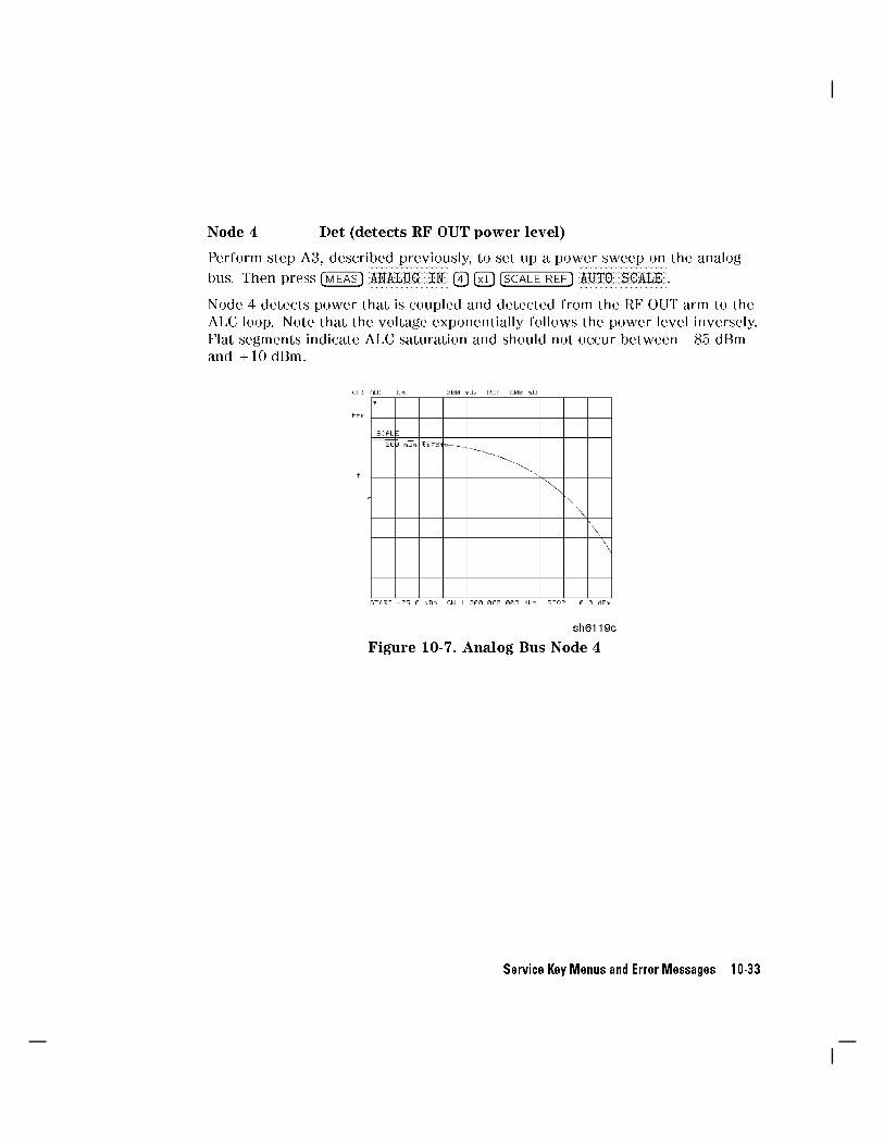
Node 4 Det (detects RF OUT power level)
Perform step A3, described previously, to set up a power sweep on the analog
bus. Then press �MEAS�NNNNNNNNNNNNNNNNNNNNNNNNNNNNNANALOG IN �4� �x1� �SCALE REF�
NNNNNNNNNNNNNNNNNNNNNNNNNNNNNNNNAUTO SCALE .
Node 4 detects power that is coupled and detected from the RF OUT arm to theALC loop. Note that the voltage exponentially follows the power level inversely.Flat segments indicate ALC saturation and should not occur between �85 dBmand +10 dBm.
Figure 10-7. Analog Bus Node 4
Service Key Menus and Error Messages 10-33
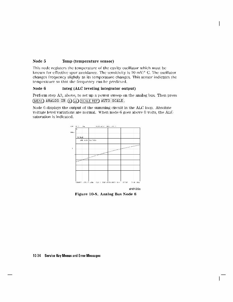
Node 5 Temp (temperature sensor)
This node registers the temperature of the cavity oscillator which must beknown for e�ective spur avoidance. The sensitivity is 10 mV/� C. The oscillatorchanges frequency slightly as its temperature changes. This sensor indicates thetemperature so that the frequency can be predicted.
Node 6 Integ (ALC leveling integrator output)
Perform step A3, above, to set up a power sweep on the analog bus. Then press
�MEAS�NNNNNNNNNNNNNNNNNNNNNNNNNNNNNANALOG IN �6� �x1� �SCALE REF�
NNNNNNNNNNNNNNNNNNNNNNNNNNNNNNNNAUTO SCALE .
Node 6 displays the output of the summing circuit in the ALC loop. Absolutevoltage level variations are normal. When node 6 goes above 0 volts, the ALCsaturation is indicated.
Figure 10-8. Analog Bus Node 6
10-34 Service Key Menus and Error Messages
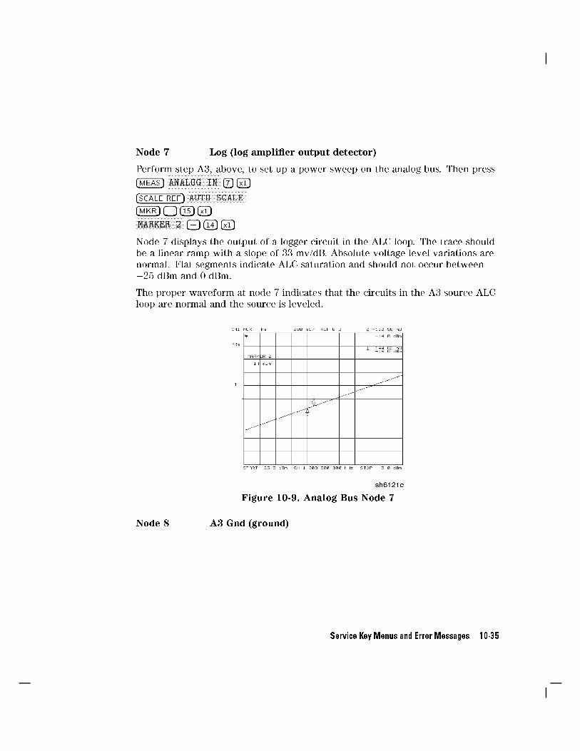
Node 7 Log (log ampli�er output detector)
Perform step A3, above, to set up a power sweep on the analog bus. Then press
�MEAS�NNNNNNNNNNNNNNNNNNNNNNNNNNNNNANALOG IN �7� �x1�
�SCALE REF�NNNNNNNNNNNNNNNNNNNNNNNNNNNNNNNNAUTO SCALE
�MKR� ��� �15� �x1�NNNNNNNNNNNNNNNNNNNNNNNNNNMARKER 2 ��� �14� �x1�
Node 7 displays the output of a logger circuit in the ALC loop. The trace shouldbe a linear ramp with a slope of 33 mv/dB. Absolute voltage level variations arenormal. Flat segments indicate ALC saturation and should not occur between�25 dBm and 0 dBm.
The proper waveform at node 7 indicates that the circuits in the A3 source ALCloop are normal and the source is leveled.
Figure 10-9. Analog Bus Node 7
Node 8 A3 Gnd (ground)
Service Key Menus and Error Messages 10-35
A10 Digital IF
To observe the A10 analog bus nodes perform step A10, below. Then follow thenode-speci�c instructions.
Step A10.Press:�PRESET�
�MEAS�NNNNNNNNNNNNNNNNNNNNNNNNNNNNNANALOG IN
�MKR�
�SYSTEM�NNNNNNNNNNNNNNNNNNNNNNNNNNNNNNNNNNNNNNSERVICE MENU
NNNNNNNNNNNNNNNNNNNNNNNNNNNNNNNNNNNNNNNNNANALOG BUS ON
Node 9 +0.37 V (+0.37 V reference)
Perform step A10, above, and then press �MEAS�NNNNNNNNNNNNNNNNNNNNNNNNNNNNNANALOG IN
NNNNNNNNNNNNNNNNNNNNNNNNNNNNNNNNNNNNNNNNNNNNNNNNNNNNNRESOLUTION [HIGH] �9� �x1�.
Check for a at line at approximately +0.37V. This is used as the voltage
reference in the \Analog Bus Correction Constants" adjustment procedure. The
voltage level should be the same in high and low resolution; the absolute level isnot critical.
Note The marker reading shows units of \mV" (millivolts).
Node 10 +2.50 V (+2.50 V reference)
Perform step A10, above, and then press �MEAS�NNNNNNNNNNNNNNNNNNNNNNNNNNNNNANALOG IN
NNNNNNNNNNNNNNNNNNNNNNNNNNNNNNNNNNNNNNNNNNNNNNNNNNRESOLUTION [LOW] �10� �x1� �SCALE REF� �1� �x1�.
Check for a at line at approximately +2.5V. This voltage is used in the \AnalogBus Correction Constants" adjustment as a reference for calibrating the analogbus low resolution circuitry.
10-36 Service Key Menus and Error Messages
Node 11 Aux Input (rear panel input)
Perform step A10, above, and then press �MEAS�NNNNNNNNNNNNNNNNNNNNNNNNNNNNNANALOG IN �1� �1� �x1�.
This selects the rear panel AUX INPUT to drive the analog bus for voltageand frequency measurements. It can be used to look at test points within theinstrument, using the analyzer's display as an oscilloscope. Connect the testpoint of interest to the rear panel AUX INPUT BNC connector.
This feature can be useful if an oscilloscope is not available. Also, it can be usedfor testing voltage-controlled devices by connecting the driving voltage of thedevice under test to the AUX IN connector. Look at the driving voltage on onedisplay channel, while displaying the S-parameter response of the test device onthe other display channel.
WithNNNNNNNNNNNNNNNNNNNNNNNAUX OUT switched ON, you can examine the analyzer's analog bus nodes
with external equipment (seeNNNNNNNNNNNNNNNNNNNNNNNNNNNNNNNNNNNNNNNNNNNNAUX OUT on OFF under the \Analog Bus Menu"
heading). For HP-IB considerations, see \HP-IB Service Mnemonic De�nitions,"
located later in this chapter.
Node 12 A10 Gnd (ground reference)
This node is used in the \Analog Bus Correction Constants" adjustment as areference for calibrating the analog bus low and high resolution circuitry.
A11 Phase Lock
To observe the A11 analog bus nodes perform step A11, below. Then follow the
node-speci�c instructions.
Step A11.Press:�PRESET�
�MEAS�NNNNNNNNNNNNNNNNNNNNNNNNNNNNNANALOG IN
�MKR�
�SYSTEM�NNNNNNNNNNNNNNNNNNNNNNNNNNNNNNNNNNNNNNSERVICE MENU
NNNNNNNNNNNNNNNNNNNNNNNNNNNNNNNNNNNNNNNNNANALOG BUS ON
Node 13 VCO Tune 2 (not used)
Service Key Menus and Error Messages 10-37

Node 14 Vbb Ref (ECL reference voltage level)
Perform step A11, above, and then press �MEAS�NNNNNNNNNNNNNNNNNNNNNNNNNNNNNANALOG IN �14� �x1� �SCALE REF�
�.3� �x1�NNNNNNNNNNNNNNNNNNNNNNNNNNNNNNNNNNNNNNNNNNNNNNNREFERENCE VALUE ��1.29� �x1�
The trace should be a at line across the entire operation frequency rangewithin 0.3 V (one division) of the reference value. Vbb Ref is used tocompensate for ECL voltage drift.
Figure 10-10. Analog Bus Node 14
10-38 Service Key Menus and Error Messages
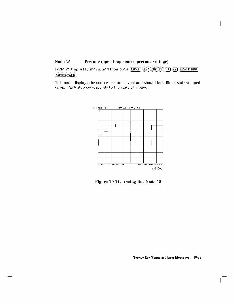
Node 15 Pretune (open-loop source pretune voltage)
Perform step A11, above, and then press �MEAS�NNNNNNNNNNNNNNNNNNNNNNNNNNNNNANALOG IN �15� �x1� �SCALE REF�
NNNNNNNNNNNNNNNNNNNNNNNNNNNNNAUTOSCALE .
This node displays the source pretune signal and should look like a stair-steppedramp. Each step corresponds to the start of a band.
Figure 10-11. Analog Bus Node 15
Service Key Menus and Error Messages 10-39
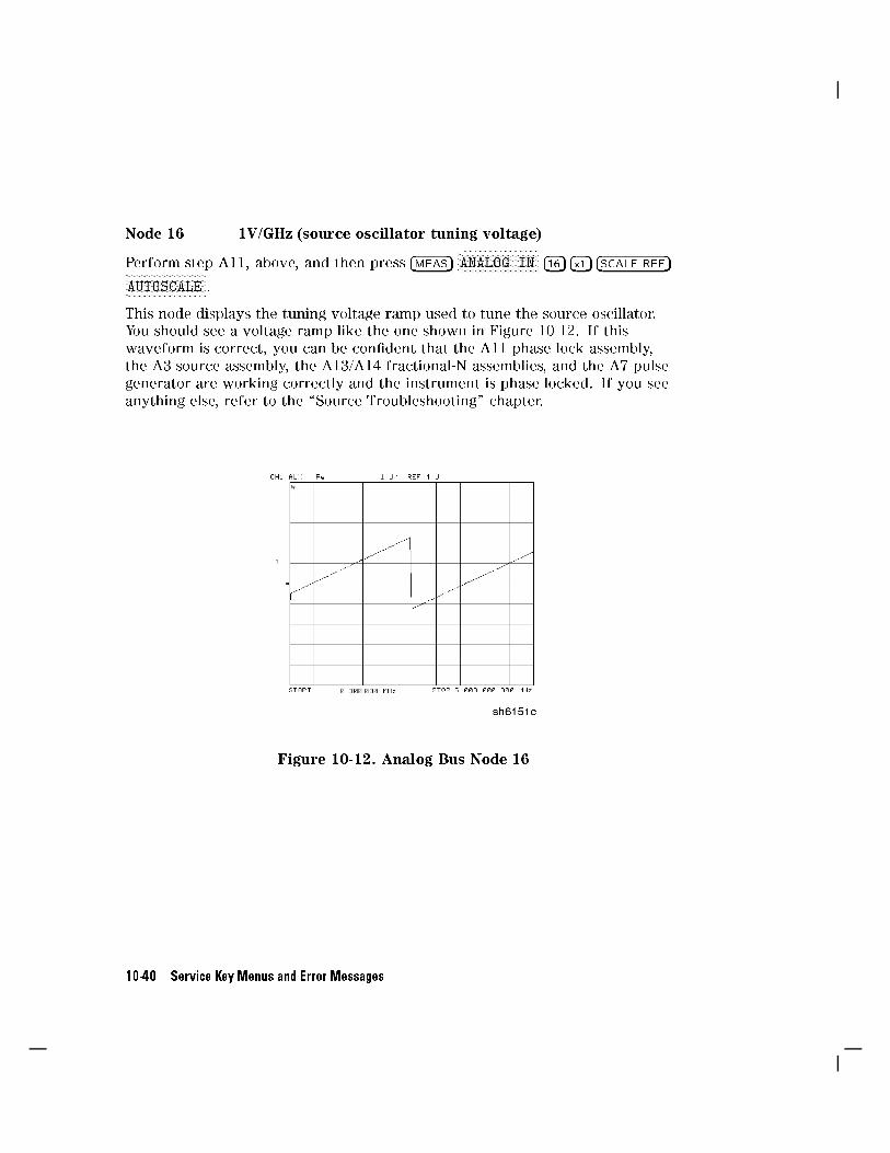
Node 16 1V/GHz (source oscillator tuning voltage)
Perform step A11, above, and then press �MEAS�NNNNNNNNNNNNNNNNNNNNNNNNNNNNNANALOG IN �16� �x1� �SCALE REF�
NNNNNNNNNNNNNNNNNNNNNNNNNNNNNAUTOSCALE .
This node displays the tuning voltage ramp used to tune the source oscillator.You should see a voltage ramp like the one shown in Figure 10-12. If thiswaveform is correct, you can be con�dent that the A11 phase lock assembly,the A3 source assembly, the A13/A14 fractional-N assemblies, and the A7 pulsegenerator are working correctly and the instrument is phase locked. If you seeanything else, refer to the \Source Troubleshooting" chapter.
Figure 10-12. Analog Bus Node 16
10-40 Service Key Menus and Error Messages

Node 17 1st IF (IF used for phase lock)
Perform step A11, above, and then press �MEAS�NNNNNNNNNNNNNNNNNNNNNNNNNNNNNANALOG IN �17� �x1�
NNNNNNNNNNNNNNNNNNNNNNNNNNNNNNNNNNNNNNNNNNNNNNNNNNNNNNNNNNNCOUNTER: ANALOG BUS �MENU�
NNNNNNNNNNNNNNNNNNNNNNNCW FREQ .
Vary the frequency and compare the results to the table below.
Entered Frequency Counter Reading
0.2 to 15.999 MHz same as entered
16 MHz to 3 GHz 1 MHz
This node displays the IF frequency (see node17) as it enters the A11 phase lockassembly via the A4 R sampler assembly. This signal comes from the R sampler
output and is used to phase lock the source.
Figure 10-13. Counter Readout Location
Service Key Menus and Error Messages 10-41

Node 18 IF Det 2N (IF on A11 phase lock after 3 MHz �lter)
Perform step A11, above, and then press �MEAS�NNNNNNNNNNNNNNNNNNNNNNNNNNNNNANALOG IN �18� �x1�
�STOP� �20� �M/��
�SCALE REF�NNNNNNNNNNNNNNNNNNNNNNNNNNNNNAUTOSCALE
�MRK� �18� �M/��
This node detects the IF within the low pass �lter/limiter. The �lter is usedduring the track and sweep sequences but never in band 1 (3.3 to 16 MHz). Thelow level (about �1.7V) means IF is in the passband of the �lter. This node canbe used with the FRAC N TUNE and SRC TUNE service modes.
Figure 10-14. Analog Bus Node 18
10-42 Service Key Menus and Error Messages

Node 19 IF Det 2W (IF after 16 MHz �lter)
Perform step A11, above, and then press �MEAS�NNNNNNNNNNNNNNNNNNNNNNNNNNNNNANALOG IN �19� �x1� �STOP� �20�
�x1� �SCALE REF� �.2� �x1�NNNNNNNNNNNNNNNNNNNNNNNNNNNNNNNNNNNNNNNNNNNNNNNREFERENCE VALUE ��1.2� �x1�.
This node detects IF after the 16 MHz �lter/limiter. The �lter is used duringpretune and acquire, but not in band 1. Normal state is a at line at about�1.7 V.
Node 20 IF Det 1 (IF after 30 MHz �lter)
Perform step A11, above and then press �MEAS�NNNNNNNNNNNNNNNNNNNNNNNNNNNNNANALOG IN �20� �x1� �SCALE REF�
�0.3� �x1�NNNNNNNNNNNNNNNNNNNNNNNNNNNNNNNNNNNNNNNNNNNNNNNREFERENCE VALUE ��1.29� �x1�.
The trace should be a at line across the entire frequency band at least 0.5 Vgreater than Vbb (node 14). The correct trace indicates the presence of IF afterthe �rst 30 MHz �lter/limiter.
Figure 10-15. Analog Bus Node 20
Service Key Menus and Error Messages 10-43
A12 Reference
To observe the A12 analog bus nodes perform step A12, below. Then follow thenode-speci�c instructions.
Step A12.Press:�PRESET�
�MEAS�NNNNNNNNNNNNNNNNNNNNNNNNNNNNNANALOG IN
�MKR�
�SYSTEM�NNNNNNNNNNNNNNNNNNNNNNNNNNNNNNNNNNNNNNSERVICE MENU
NNNNNNNNNNNNNNNNNNNNNNNNNNNNNNNNNNNNNNNNNANALOG BUS ON
Node 21 100 kHz (100 kHz reference frequency)
Perform step A12, above, and then press �MEAS�NNNNNNNNNNNNNNNNNNNNNNNNNNNNNANALOG IN �21� �x1�NNNNNNNNNNNNNNNNNNNNNNNNNNNNNNNNNNNNNNNNNNNNNNNNNNNNNNNNNNN
COUNTER: ANALOG BUS . This node counts the A12 100 kHz reference signal
that is used on A13 (the fractional-N analog assembly) as a reference frequencyfor the phase detector.
Node 22 A12 Gnd 1 (ground)
10-44 Service Key Menus and Error Messages
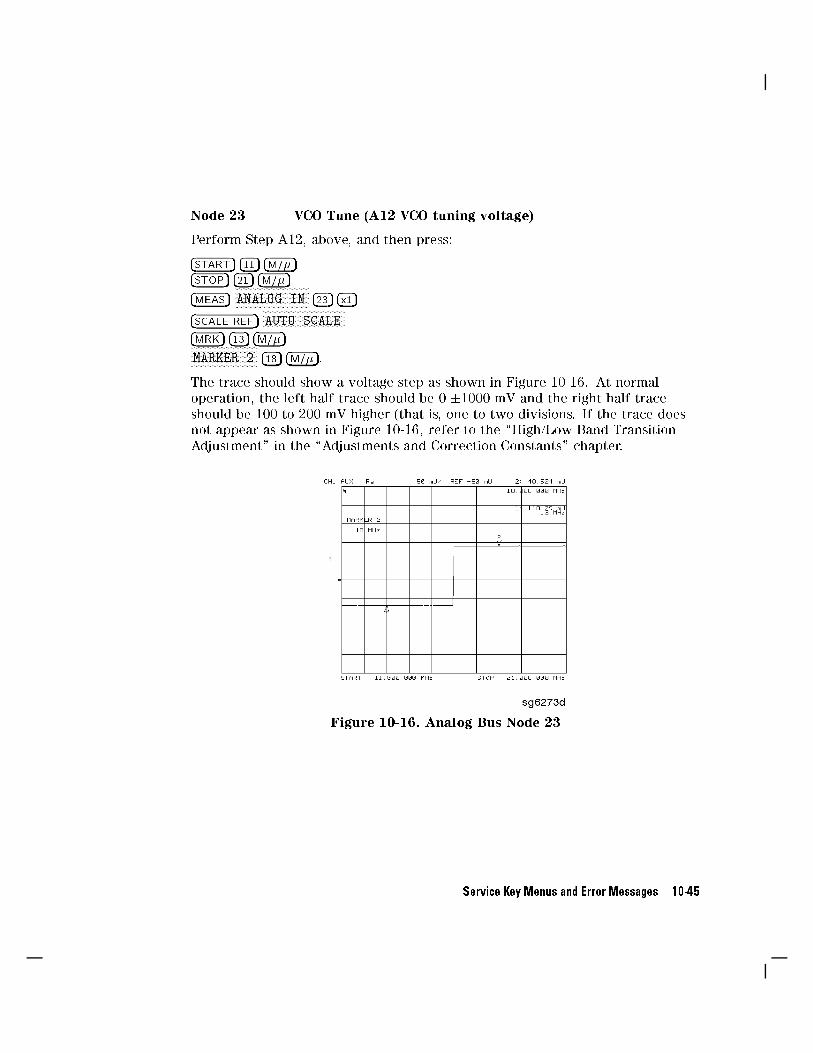
Node 23 VCO Tune (A12 VCO tuning voltage)
Perform Step A12, above, and then press:
�START� �11� �M/���STOP� �21� �M/��
�MEAS�NNNNNNNNNNNNNNNNNNNNNNNNNNNNNANALOG IN �23� �x1�
�SCALE REF�NNNNNNNNNNNNNNNNNNNNNNNNNNNNNNNNAUTO SCALE
�MRK� �13� �M/��NNNNNNNNNNNNNNNNNNNNNNNNNNMARKER 2 �18� �M/��.
The trace should show a voltage step as shown in Figure 10-16. At normaloperation, the left half trace should be 0 �1000 mV and the right half trace
should be 100 to 200 mV higher (that is, one to two divisions. If the trace doesnot appear as shown in Figure 10-16, refer to the \High/Low Band Transition
Adjustment" in the \Adjustments and Correction Constants" chapter.
Figure 10-16. Analog Bus Node 23
Service Key Menus and Error Messages 10-45

Node 24 2nd LO
Perform step A12, above, and then press �MEAS�NNNNNNNNNNNNNNNNNNNNNNNNNNNNNANALOG IN �24� �x1�NNNNNNNNNNNNNNNNNNNNNNNNNNNNNNNNNNNNNNNNNNNNNNNNNNNNNNNNNNN
COUNTER: ANALOG BUS �MENU�NNNNNNNNNNNNNNNNNNNNNNNCW FREQ .
This node counts the 2nd LO used by the sampler/mixer assemblies to producethe 2nd IF of 4 kHz. As you vary the frequency, the counter reading shouldchange to values very close to those indicated below:
Frequency Entered Counter Reading
0.03 to 1 MHz frequency entered +4 kHz
1 to 16 MHz not accurate
16 MHz to 6 GHz 1 MHz
Node 25 PL Ref (phase lock reference)
Perform step A12, above, and then press �MEAS�NNNNNNNNNNNNNNNNNNNNNNNNNNNNNANALOG IN �25� �x1�NNNNNNNNNNNNNNNNNNNNNNNNNNNNNNNNNNNNNNNNNNNNNNNNNNNNNNNNNNN
COUNTER: ANALOG BUS �MENU�NNNNNNNNNNNNNNNNNNNNNNNCW FREQ .
This node counts the reference signal used by the phase comparator circuit onthe A11 phase lock assembly. As you vary the frequency, the counter reading
should change as indicated below:
Frequency Entered Counter Reading
0.3 to 1 MHz frequency entered
1 to 16 MHz not accurate
16 MHz to 6 GHz 1 MHz
10-46 Service Key Menus and Error Messages

Node 26 Ext Ref (rear panel external reference input)
Perform step A12, above, and then press �MEAS�NNNNNNNNNNNNNNNNNNNNNNNNNNNNNANALOG IN �26� �x1�.
The voltage level of this node indicates whether an external reference timebaseis being used:
No external reference: about �0.9VWith external reference: about �0.6V.
Node 27 VCXO Tune (40 MHz VCXO tuning voltage)
Perform step A12, above, and then press �MEAS�NNNNNNNNNNNNNNNNNNNNNNNNNNNNNANALOG IN �27� �x1� �MKR FCTN�NNNNNNNNNNNNNNNNNNNNNNNNNNNNNNNNNNNNNNNNNNNNNNNNNNNNNNN
MARKER !REFERENCE .
This node displays the voltage used to �ne tune the A12 reference VCXO to40 MHz. You should see a at line at some voltage level (the actual voltage level
varies from instrument to instrument). Anything other than a at line indicates
that the VCXO is tuning to di�erent frequencies. Refer to the \Frequency
Accuracy" adjustment procedure.
Node 28 A12 Gnd 2 (Ground reference)
A14 Fractional-N (Digital)
To observe the A14 analog bus nodes perform step A14, below. Then follow the
node-speci�c instructions.
Step A14.Press:�PRESET�
�MEAS�NNNNNNNNNNNNNNNNNNNNNNNNNNNNNANALOG IN
�SYSTEM�NNNNNNNNNNNNNNNNNNNNNNNNNNNNNNNNNNNNNNSERVICE MENU
NNNNNNNNNNNNNNNNNNNNNNNNNNNNNNNNNNNNNNNNNANALOG BUS ON
Service Key Menus and Error Messages 10-47

Node 29 FN VCO Tun (A14 FN VCO tuning voltage)
Perform step A14, above, and then press �MEAS�NNNNNNNNNNNNNNNNNNNNNNNNNNNNNANALOG IN �29� �x1� �SCALE REF�NNNNNNNNNNNNNNNNNNNNNNNNNNNNN
AUTOSCALE .
Observe the A14 FN VCO tuning voltage. If the A13 and A14 assemblies arefunctioning correctly and the VCO is phase locked, the trace should look likeFigure 10-17. Any other waveform indicates that the FN VCO is not phaselocked. The vertical lines in the trace indicate the band crossings. (The countercan also be enabled to count the VCO frequency in CW mode.)
Figure 10-17. Analog Bus Node 29
10-48 Service Key Menus and Error Messages
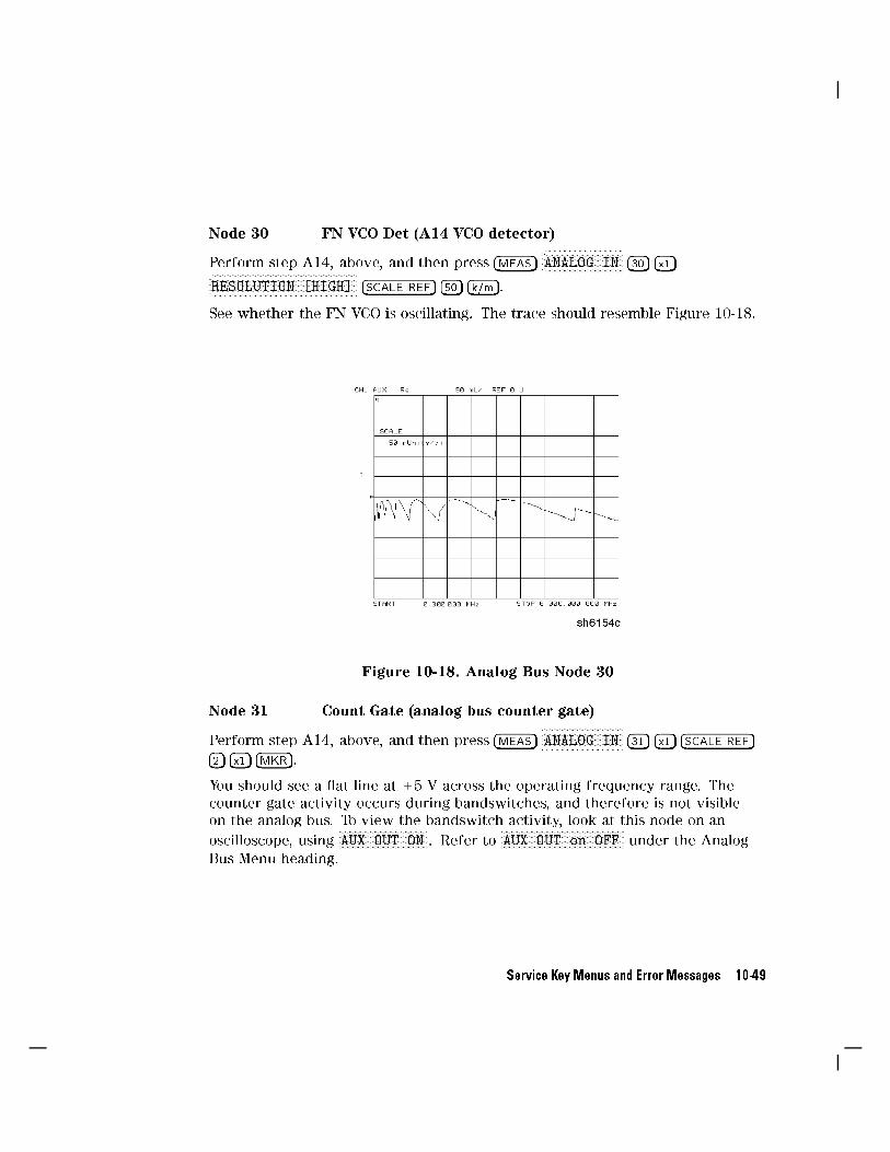
Node 30 FN VCO Det (A14 VCO detector)
Perform step A14, above, and then press �MEAS�NNNNNNNNNNNNNNNNNNNNNNNNNNNNNANALOG IN �30� �x1�
NNNNNNNNNNNNNNNNNNNNNNNNNNNNNNNNNNNNNNNNNNNNNNNNNNNNNRESOLUTION [HIGH] �SCALE REF� �50� �k/m�.
See whether the FN VCO is oscillating. The trace should resemble Figure 10-18.
Figure 10-18. Analog Bus Node 30
Node 31 Count Gate (analog bus counter gate)
Perform step A14, above, and then press �MEAS�NNNNNNNNNNNNNNNNNNNNNNNNNNNNNANALOG IN �31� �x1� �SCALE REF�
�2� �x1� �MKR�.
You should see a at line at +5 V across the operating frequency range. Thecounter gate activity occurs during bandswitches, and therefore is not visibleon the analog bus. To view the bandswitch activity, look at this node on an
oscilloscope, usingNNNNNNNNNNNNNNNNNNNNNNNNNNNNNNNNAUX OUT ON . Refer to
NNNNNNNNNNNNNNNNNNNNNNNNNNNNNNNNNNNNNNNNNNNNAUX OUT on OFF under the Analog
Bus Menu heading.
Service Key Menus and Error Messages 10-49

PEEK/POKE Menu
To access this menu, press �SYSTEM�NNNNNNNNNNNNNNNNNNNNNNNNNNNNNNNNNNNNNNSERVICE MENU
NNNNNNNNNNNNNNNNNNNNNNNNNNNNNPEEK/POKE .
NNNNNNNNNNNNNNNNNNNNNNNNNNNNNPEEK/POKE Allows you to edit the content of one or more
memory
addresses. The keys are described below.
Caution The PEEK/POKE capability is intended for service use only.
NNNNNNNNNNNNNNNNNNNNNNNNNNNNNNNNNNNNNNNNNNNNNNNNNNNNNPEEK/POKE ADDRESS(PEEL[D])
accesses any memory address and shows it in theactive entry area of the display. Use the front panel
knob, entry keys, or step keys to enter the memoryaddress of interest.
NNNNNNNNNNNNNNPEEK (PEEK) Displays the data at the accessed memory address.
NNNNNNNNNNNNNNPOKE (POKE[D]) allows you to change the data at the memory
address accessed by theNNNNNNNNNNNNNNNNNNNNNNNNNNNNNNNNNNNNNNNNNNNNNNNNNNNNNPEEK/POKE ADDRESS
softkey. Use the front panel knob, entry keys, orstep keys to change the data. The A9CC jumpermust be in the \ALTER" position in order to poke.
NNNNNNNNNNNNNNNNNNNNNNNNNNNNNNNNNNNNNNRESET MEMORY Resets or clears the memory where instrument
states are stored. To do this, pressNNNNNNNNNNNNNNNNNNNNNNNNNNNNNNNNNNNNNNRESET MEMORY
�PRESET�.
10-50 Service Key Menus and Error Messages

Firmware Revision Softkey
Press �SYSTEM�NNNNNNNNNNNNNNNNNNNNNNNNNNNNNNNNNNNNNNSERVICE MENU
NNNNNNNNNNNNNNNNNNNNNNNNNNNNNNNNNNNNNNNNNNNNNNNNNNNNNFIRMWARE REVISION to display the current
�rmware revision information. The number and implementation date appearin the active entry area of the display as shown in Figure 10-19 below. Theanalyzer's serial number and installed options are also displayed. Another wayto display the �rmware revision information is to cycle the line power.
Figure 10-19. Location of Firmware Revision Information on Display
Service Key Menus and Error Messages 10-51

HP-IB Service Mnemonic De�nitions
All service routine keystrokes can be made through HP-IB in one of thefollowing approaches:
sending equivalent remote HP-IB commands (Mnemonics have beendocumented previously with the corresponding keystroke.)
invoking the System Menu (MENUSYST) and using the analyzer mnemonic(SOFTn), where \n" represents the softkey number. (Softkeys arenumbered 1 to 8 from top to bottom.)
An HP-IB overview is provided in the \Compatible Peripherals" chapter inthe User's Guide. HP-IB programming information is also provided in the
Programming Guide.
Invoking Tests Remotely
Many tests require a response to the displayed prompts. Since bit 1 of the Event
Status Register B is set (bit 1 = service routine waiting) any time a serviceroutine prompts the user for an expected response, you can send an appropriate
response using one of the following techniques:
Read event status register B to reset the bit.
Enable bit 1 to interrupt (ESNB[D]). See \Status Reporting" in theProgramming Guide.
Respond to the prompt with a TESRn command (see Tests Menu, at the
beginning of this chapter).
Symbol Conventions
[ ] An optional operand
D A numerical operand
< > A necessary appendage
j An either/or choice in appendages
10-52 Service Key Menus and Error Messages

Analog Bus Codes
ANAI[D] Measures and displays the analog input. The preset stateinput to the analog bus is the rear panel AUX IN. The other
30 nodes may be selected withNNNNND only if the ABUS is
enabled (ANABon).
OUTPCNTR Outputs the counter's frequency data.
OUTPERRO Reads any prompt message sent to the error queue by aservice routine.
OUTPTESS Outputs the integer status of the test most recentlyexecuted. Status codes are those listed under \TST?".
TST? Executes the power-on self test (internal test 1) and
outputs an integer test status. Status codes are as follows:
0 =pass
1 =fail
2 =in progress
3 =not available
4 =not done
5 =done
Service Key Menus and Error Messages 10-53

Error Messages
This section contains an alphabetical list of the error messages that pertain toservicing the analyzer. The information in the list includes explanations of thedisplayed messages and suggestion to help solve the problem.
Note The error messages that pertain to measurement applicationsare included in the HP 8752C Network Analyzer User's Guide.
BATTERY FAILED. STATE MEMORY CLEARED
Error Number183
The battery protection of the non-volatile CMOS memory hasfailed. The CMOS memory has been cleared. The battery shouldbe replaced. See the \Preset State and Memory Allocation,"chapter in the HP 8752C Network Analyzer User's Guide for
more information about the CMOS memory.
BATTERY LOW! STORE SAVE REGS TO DISK
Error Number184
The battery protection of the non-volatile CMOS memory is indanger of failing. If this occurs, all of the instrument state
registers stored in CMOS memory will be lost. Save these statesto a disk and refer to the \Assembly Replacement andPost-Repair Procedures" chapter for battery replacementinstructions. See the \Preset State and Memory Allocation,"
chapter in the HP 8752C Network Analyzer User's Guide formore information about the CMOS memory.
CALIBRATION ABORTED
Error Number74
You have changed the active channel during a calibration so thecalibration in progress was terminated. Make sure theappropriate channel is active and restart the calibration.
10-54 Service Key Menus and Error Messages

CALIBRATION REQUIRED
Error Number63
A calibration set could not be found that matched the currentstimulus state or measurement parameter. You will have toperform a new calibration.
CORRECTION CONSTANTS NOT STORED
Error Number3
A store operation to the EEPROM was not successful. You mustchange the position of the jumper on the A9 CPU assembly.
Refer to the \A9 CC Jumper Position Procedure" in the\Adjustments and Correction Constants" chapter.
CORRECTION TURNED OFF
Error Number66
Critical parameters in your current instrument state do notmatch the parameters for the calibration set, thereforecorrection has been turned o�. The critical instrument stateparameters are sweep type, start frequency, frequency span,
and number of points.
CURRENT PARAMETER NOT IN CAL SET
Error Number64
Correction is not valid for your selected measurementparameter. Either change the measurement parameters orperform a new calibration.
DEADLOCK
Error Number111
A fatal �rmware error occurred before instrument presetcompleted.
Service Key Menus and Error Messages 10-55

DEVICE: not on, not connect, wrong addrs
Error Number119
The device at the selected address cannot be accessed by theanalyzer. Verify that the device is switched on, and check theHP-IB connection between the analyzer and the device. Ensurethat the device address recognized by the analyzer matches theHP-IB address set on the device itself.
DISK HARDWARE PROBLEM
Error Number39
The disk drive is not responding correctly. Refer to the disk
drive operating manual.
DISK MESSAGE LENGTH ERROR
Error Number190
The analyzer and the external disk drive aren't communicatingproperly. Check the HP-IB connection and then try substituting
another disk drive to isolate the problem instrument.
DISK: not on, not connected, wrong addrs
Error Number
38
The disk cannot be accessed by the analyzer. Verify power to
the disk drive, and check the HP-IB connection between theanalyzer and the disk drive. Ensure that the disk drive addressrecognized by the analyzer matches the HP-IB address set onthe disk drive itself.
10-56 Service Key Menus and Error Messages

DISK READ/WRITE ERROR
Error Number189
There may be a problem with your disk. Try a new oppy disk.If a new oppy disk does not eliminate the error, suspecthardware problems.
INITIALIZATION FAILED
Error Number47
The disk initialization failed, probably because the disk isdamaged.
NO CALIBRATION CURRENTLY IN PROGRESS
Error Number69
TheNNNNNNNNNNNNNNNNNNNNNNNNNNNNNNNNNNNNNNNNNNNNNNNNNNNNNNNNNNNRESUME CAL SEQUENCE softkey is not valid unless a
calibration is already in progress. Start a new calibration.
NOT ENOUGH SPACE ON DISK FOR STORE
Error Number44
The store operation will over ow the available disk space.
Insert a new disk or purge �les to create free disk space.
NO FILE(S) FOUND ON DISK
Error Number45
No �les of the type created by an analyzer store operation werefound on the disk. If you requested a speci�c �le title, that �le
was not found on the disk.
Service Key Menus and Error Messages 10-57

NO IF FOUND: CHECK R INPUT LEVEL
Error Number5
The �rst IF signal was not detected during pretune. Check thefront panel R channel jumper. If there is no visible problemwith the jumper, refer to the \Source Troubleshooting" chapter.
NO PHASE LOCK: CHECK R INPUT LEVEL
Error Number7
The �rst IF signal was detected at pretune, but phase lock couldnot be acquired. Refer to the \Source Troubleshooting" chapter.
NO SPACE FOR NEW CAL. CLEAR REGISTERS
Error Number70
You cannot store a calibration set due to insu�cient memory.
You can free more memory by clearing a saved instrument state
from an internal register (which may also delete an associated
calibration set, if all the instrument states using the calibration
kit have been deleted.) You can store the saved instrument stateand calibration set to a disk before clearing them. After deletingthe instrument states, press �PRESET� to run the memory packer.
OVERLOAD ON REFL PORT, POWER REDUCED
Error Number58
You have exceeded approximately +20 dBm at the re ectionport. The RF output power is automatically reduced to�20 dBm. The annotation P# appears in the left margin of thedisplay to indicate that the power trip function has beenactivated. When this occurs, reset the power to a lower level,
then toggle theNNNNNNNNNNNNNNNNNNNNNNNNNNNNNNNNNNNNNNNNNNNNNNNNNNNNNSOURCE PWR on OFF softkey to switch the
power back on.
10-58 Service Key Menus and Error Messages
OVERLOAD ON TRANS PORT, POWER REDUCED
Error Number59
You have exceeded approximately +4 dBm at the re ectionport. The RF output power is automatically reduced to�20 dBm. The annotation P# appears in the left margin of thedisplay to indicate that the power trip function has beenactivated. When this occurs, reset the power to a lower level,
then toggle theNNNNNNNNNNNNNNNNNNNNNNNNNNNNNNNNNNNNNNNNNNNNNNNNNNNNNSOURCE PWR on OFF softkey to switch the
power back on.
OVERLOAD ON INPUT R, POWER REDUCED
Error Number57
You have exceeded approximately +17 dBm at the re ectionport. The RF output power is automatically reduced to�20 dBm. The annotation P# appears in the left margin of the
display to indicate that the power trip function has been
activated. When this occurs, reset the power to a lower level,
then toggle theNNNNNNNNNNNNNNNNNNNNNNNNNNNNNNNNNNNNNNNNNNNNNNNNNNNNNSOURCE PWR on OFF softkey to switch the
power back on.
PHASE LOCK CAL FAILED
Error Number4
An internal phase lock calibration routine is automaticallyexecuted at power-on, preset, and any time a loss of phase lockis detected. This message indicates that phase lock calibrationwas initiated and the �rst IF detected, but a problem preventedthe calibration from completing successfully. Refer toChapter 3, \Adjustments and Correction Constants" and executepretune correction (test 48).
Service Key Menus and Error Messages 10-59

PHASE LOCK LOST
Error Number8
Phase lock was acquired but then lost. Refer to the \SourceTroubleshooting" chapter.
POSSIBLE FALSE LOCK
Error Number6
Phase lock has been achieved, but the source may be phaselocked to the wrong harmonic of the synthesizer. Perform thesource pretune correction routine documented in the\Adjustments and Correction Constants" chapter.
POWER UNLEVELED
Error Number179
There is either a hardware failure in the source or you haveattempted to set the power level too high. Check to see if thepower level you set is within speci�cations. If it is, refer to the
\Source Troubleshooting" chapter. You will only receive this
message over the HP-IB. On the analyzer, P? is displayed.
POW MET INVALID
Error Number
116
The power meter indicates an out-of-range condition. Check the
test setup.
POW MET NOT SETTLED
Error Number118
Sequential power meter readings are not consistent. Verify that
the equipment is set up correctly. If so, preset the instrument
and restart the operation.
10-60 Service Key Menus and Error Messages
POW MET: not on, not connected, wrong addrs
Error Number117
The power meter cannot be accessed by the analyzer. Verifythat the power meter address and model number set in theanalyzer match the address and model number of the actualpower meter.
POWER SUPPLY HOT!
Error Number21
The temperature sensors on the A8 post-regulator assemblyhave detected an over-temperature condition. The powersupplies regulated on the post-regulator have been shut down.Refer to the \Power Supply Troubleshooting" chapter.
POWER SUPPLY SHUT DOWN!
Error Number22
One or more supplies on the A8 post-regulator assembly havebeen shut down due to an over-current, over-voltage, or
under-voltage condition. Refer to the \Power SupplyTroubleshooting" chapter.
PRINTER: not on, not connected, wrong addrs
Error Number24
The printer does not respond to control. Verify power to theprinter, and check the HP-IB connection between the analyzerand the printer. Ensure that the printer address recognized bythe analyzer matches the HP-IB address set on the printer itself.
Service Key Menus and Error Messages 10-61

PROBE POWER SHUT DOWN!
Error Number23
The analyzer biasing supplies to the HP 85024A external probeare shut down due to excessive current. Troubleshoot theprobe, and refer to the \Power Supply Troubleshooting" chapter.
SAVE FAILED. INSUFFICIENT MEMORY
Error Number151
You cannot store an instrument state in an internal register dueto insu�cient memory. Increase the available memory by
clearing one or more save/recall registers and pressing �PRESET�,or by storing �les to a disk.
SELF TEST #n FAILED
Service ErrorNumber 112
Internal test #n has failed. Several internal test routines areexecuted at instrument preset. The analyzer reports the �rstfailure detected. Refer to the internal tests and theself-diagnose feature descriptions earlier in this chapter.
SOURCE POWER TRIPPED, RESET UNDER POWER MENU
InformationMessage
You have exceeded the maximum power level at one of theinputs and power has been automatically reduced. Theannotation P+ indicates that power trip has been activated.
When this occurs, reset the power and then press �MENU�NNNNNNNNNNNNNNNNNPOWER
NNNNNNNNNNNNNNNNNNNNNNNNNNNNNNNNNNNNNNNNNNNNNNNNNNNNNSOURCE PWR on OFF , to switch on the power. This message
follows error numbers 57, 58, and 59.
10-62 Service Key Menus and Error Messages

SYSTEM IS NOT IN REMOTE
Error Number52
The analyzer is in local mode. In this mode, the analyzer willnot respond to HP-IB commands with front panel keyequivalents. It will, however, respond to commands that haveno such equivalents, such as status requests.
SWEEP MODE CHANGED TO CW TIME SWEEP
Error Number187
If you select external source auto or manual instrument modeand you do not also select CW mode, the analyzer is
automatically switched to CW.
TEST ABORTED
Error Number113
You have prematurely stopped a service test.
TROUBLE! CHECK SETUP AND START OVER
Service ErrorNumber 115
Your equipment setup for the adjustment procedure in progressis not correct. Check the setup diagram and instructions in the\Adjustments and Correction Constants" chapter. Start the
procedure again.
WRONG DISK FORMAT, INITIALIZE DISK
Error Number77
You have attempted to store, load, or read �le titles, but your
disk format does not conform to the Logical Interchange Format
(LIF). You must initialize the disk before reading or writing to it.
Service Key Menus and Error Messages 10-63


11
Error Terms
The analyzer generates and stores factors in internal arrays when ameasurement error-correction (measurement calibration) is performed. Thesefactors are known by the following terms:
error termsE-termsmeasurement calibration coe�cients
The analyzer creates error terms by measuring well-de�ned calibration devicesover the frequency range of interest and comparing the measured data with theideal model for the devices. The di�erences represent systematic (repeatable)
errors of the analyzer system. The resulting calibration coe�cients are goodrepresentations of the systematic error sources. For details on the various levels
of error-correction, refer to the \Optimizing Measurement Results" chapter of
the HP 8752C Network Analyzer User's Guide. For details on the theory of
error-correction, refer to the \Application and Operation Concepts" chapter ofthe HP 8752C Network Analyzer User's Guide.
Error Terms 11-1

Error Terms Can Also Serve a Diagnostic Purpose
Speci�c parts of the analyzer and its accessories directly contribute to thecharacteristics of the error terms. Since we know this correlation and we knowwhat typical error terms look like, we can examine error terms to monitorsystem performance (preventive maintenance) or to identify faulty componentsin the system (troubleshooting).
Preventive Maintenance: A stable, repeatable system should generaterepeatable error terms over long time intervals, for example, six months.If you make a hardcopy record (print or plot) of the error terms, you canperiodically compare current error terms with the record. A sudden shift inthe values of the error terms re ects a sudden shift in systematic errors, and
may indicate the need for further troubleshooting. A long-term trend oftenre ects drift, connector and cable wear, or gradual degradation, indicating the
need for further investigation and preventive maintenance. Yet, the systemmay still conform to speci�cations. The cure is often as simple as cleaning and
gaging connectors or inspecting cables.
Troubleshooting: If a subtle failure or mild performance problem is
suspected, the magnitude of the error terms should be compared against
values generated previously with the same instrument and calibration kit.This comparison will produce the most precise view of the problem.
However, if previously generated values are not available, compare the
current values to the typical values listed in Table 11-2, and shown graphically
on the plots in this chapter. If the magnitude exceeds its limit, inspect the
corresponding system component, which may ultimately need replacing.
Consider the following while troubleshooting:
All parts of the system, including cables and calibration devices, cancontribute to systematic errors and impact the error terms.
Connectors must be clean, gaged, and within speci�cation for error termanalysis to be meaningful.
Avoid unnecessary bending and exing of the cables following measurement
calibration, minimizing cable instability errors.
Use good connection techniques during the measurement calibration.The connector interface must be repeatable. Refer to the \Principles
of Microwave Connector Care" section in the \Service Equipment and
Analyzer Options" chapter for information on connection techniques and on
cleaning and gaging connectors.
11-2 Error Terms

Use error term analysis to troubleshoot minor, subtle performance problems.Refer to the \Start Troubleshooting Here" chapter if a blatant failure orgross measurement error is evident.
It is often worthwhile to perform the procedure twice (using two distinctmeasurement calibrations) to establish the degree of repeatability. If theresults do not seem repeatable, check all connectors and cables.
Error Terms 11-3

Re ection 1-Port Error-Correction Procedure
1. Set any measurement parameters that you want for the devicemeasurement: power, format, number of points, IF bandwidth.
2. To access the measurement correction menus, press:
�CAL�
3. Assuming that your calibration kit is the N 50 default, press:NNNNNNNNNNNNNNNNNNNNNNNCAL KIT
NNNNNNNNNNNNNNNNNN 50
NNNNNNNNNNNNNNNNNNNNRETURN
4. To select the correction type, press:NNNNNNNNNNNNNNNNNNNNNNNNNNNNNNNNNNNNNNNNNNNNCALIBRATE MENU
NNNNNNNNNNNNNNNNNNNNNNNNNNNNNNNNNNNNNNNNNNNNNNNNNNNNNREFLECTION 1-PORT
5. Connect a shielded open circuit to the REFLECTION port. See Figure 11-1.
Figure 11-1. Standard Connections for One-Port Error-Correction
11-4 Error Terms

6. To measure the standard, press:NNNNNNNNNNNNNNNNNNNNNNNNNNNNNNNNNNNNNNNNNNNNFORWARD: OPENS
NNNNNNNNNNNNNNNNNNNNNNNNNNOPEN (f)
When the analyzer is done measuring the standard, press:NNNNNNNNNNNNNNNNNNNNNNNNNNNNNNNNNNNDONE: OPENS
7. Disconnect the open, and connect a short circuit to the REFLECTION port.
8. To measure the device, press:NNNNNNNNNNNNNNNNNNNNNNNNNNNNNNNNNNNNNNNNNNNNNNNFORWARD: SHORTS
NNNNNNNNNNNNNNNNNNNNNNNNNNNNNSHORT (f)
After the beep, press:NNNNNNNNNNNNNNNNNNNNNNNNNNNNNNNNNNNNNNDONE: SHORTS
9. Disconnect the short, and connect an impedance-matched load to theREFLECTION port.
10. To measure the standard, press:NNNNNNNNNNNNNNNNNNNNNNNNNNNNNNNNNNNNNNNNNFORWARD: LOAD
The analyzer underlines theNNNNNNNNNNNNNNLOAD softkey after it measures the standard.
11. To compute the re ection correction coe�cients, press:NNNNNNNNNNNNNNNNNNNNNNNNNNNNNNNNNNNNNNNNNNNNNNNNNNDONE: 1-PORT CAL
Error Terms 11-5

Response and Isolation Calibration Procedures
1. Press �MEAS�NNNNNNNNNNNNNNNNNNNNNNNNNNNNNNNNTRANSMISSN .
2. PressNNNNNNNNNNNCAL
NNNNNNNNNNNNNNNNNNNNNNNCAL KIT
NNNNNNNNNNNNNNNNNN 50
NNNNNNNNNNNNNNNNNNNNRETURN .
3. PressNNNNNNNNNNNNNNNNNNNNNNNNNNNNNNNNNNNNNNNNNNNNCALIBRATE MENU
NNNNNNNNNNNNNNNNNNNNNNNNNNNNNNNNNNNNNNNNNNNNNNNNNNNNNRESPONSE & ISOL'N .
4. PressNNNNNNNNNNNNNNNNNNNNNNNNNNRESPONSE .
5. Connect equipment as shown in Figure 11-2.
Figure 11-2. Standard Connections for Response Calibration
6. PressNNNNNNNNNNNNNNTHRU .
7. After the beep, pressNNNNNNNNNNNNNNNNNNNNNNNNNNNNNNNNNNNNNNNNNNNNDONE: RESPONSE .
8. Connect the equipment as shown in Figure 11-3.
11-6 Error Terms
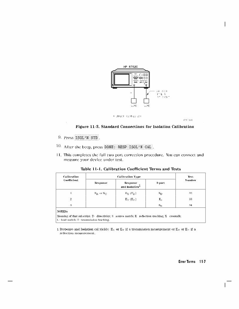
Figure 11-3. Standard Connections for Isolation Calibration
9. PressNNNNNNNNNNNNNNNNNNNNNNNNNNNNNNNNISOL'N STD .
10. After the beep, pressNNNNNNNNNNNNNNNNNNNNNNNNNNNNNNNNNNNNNNNNNNNNNNNNNNNNNNNNNNNNNNNNNDONE: RESP ISOL'N CAL .
11. This completes the full two-port correction procedure. You can connect and
measure your device under test.
Table 11-1. Calibration Coe�cient Terms and Tests
Calibration
Coe�cient
Calibration Type Test
NumberResponse Response
and Isolation11-port
1 ER or ET EX (ED) ED 32
2 ET (ER) ES 33
3 ER 34
NOTES:
Meaning of �rst subscript: D=directivity; S=source match; R=re ection tracking; X=crosstalk;
L=load match; T=transmission tracking.
1 Response and Isolation cal yields: EX or ET if a transmission measurement or ED or ER if a
re ection measurement.
Error Terms 11-7
Error Term Inspection
Note If the correction is not active, press �CAL�NNNNNNNNNNNNNNNNNNNNNNNNNNNNNNNNNNNNNNNNNCORRECTION ON .
1. Press �SYSTEM�NNNNNNNNNNNNNNNNNNNNNNNNNNNNNNNNNNNNNNSERVICE MENU
NNNNNNNNNNNNNNNNNTESTS �32� �x1�
NNNNNNNNNNNNNNNNNNNNNNNNNNNNNNNNNNNNNNEXECUTE TEST .
The analyzer copies the �rst calibration measurement trace for the selected
error term into memory and then displays it. Table 11-2 lists the testnumbers.
2. Press �SCALE REF� and adjust the scale and reference to study the error term
trace.
3. Press �MKR FCTN� and use the marker functions to determine the error term
magnitude.
4. Compare the displayed measurement trace to the trace shown in thefollowing \Error Term descriptions" section, and to previously measured
data. If data is not available from previous measurements, refer to the
typical uncorrected performance speci�cations listed in Table 11-2.
5. Make a hardcopy of the measurement results:
a. Connect a printing or plotting peripheral to the analyzer.
b. Press �LOCAL�NNNNNNNNNNNNNNNNNNNNNNNNNNNNNNNNNNNNNNNNNNNNNNNNNNNNNSYSTEM CONTROLLER
NNNNNNNNNNNNNNNNNNNNNNNNNNNNNNNNNNNNNNNNNSET ADDRESSES and select the
appropriate peripheral to verify that the HP-IB address is set correctly onthe analyzer.
c. Press �SAVE/RECALL� and then choose eitherNNNNNNNNNNNNNNNNNPRINT or
NNNNNNNNNNNNNNPLOT .
d. Press �DISPLAY�NNNNNNNNNNNNNNMORE
NNNNNNNNNNNNNNNNNTITLE and title each data trace so that you can
identify it later.
for detailed information on creating hardcopies, refer to \Printing,
Plotting, and Saving Measurement Results" in the HP 8752C Network
Analyzer User's Guide.
11-8 Error Terms
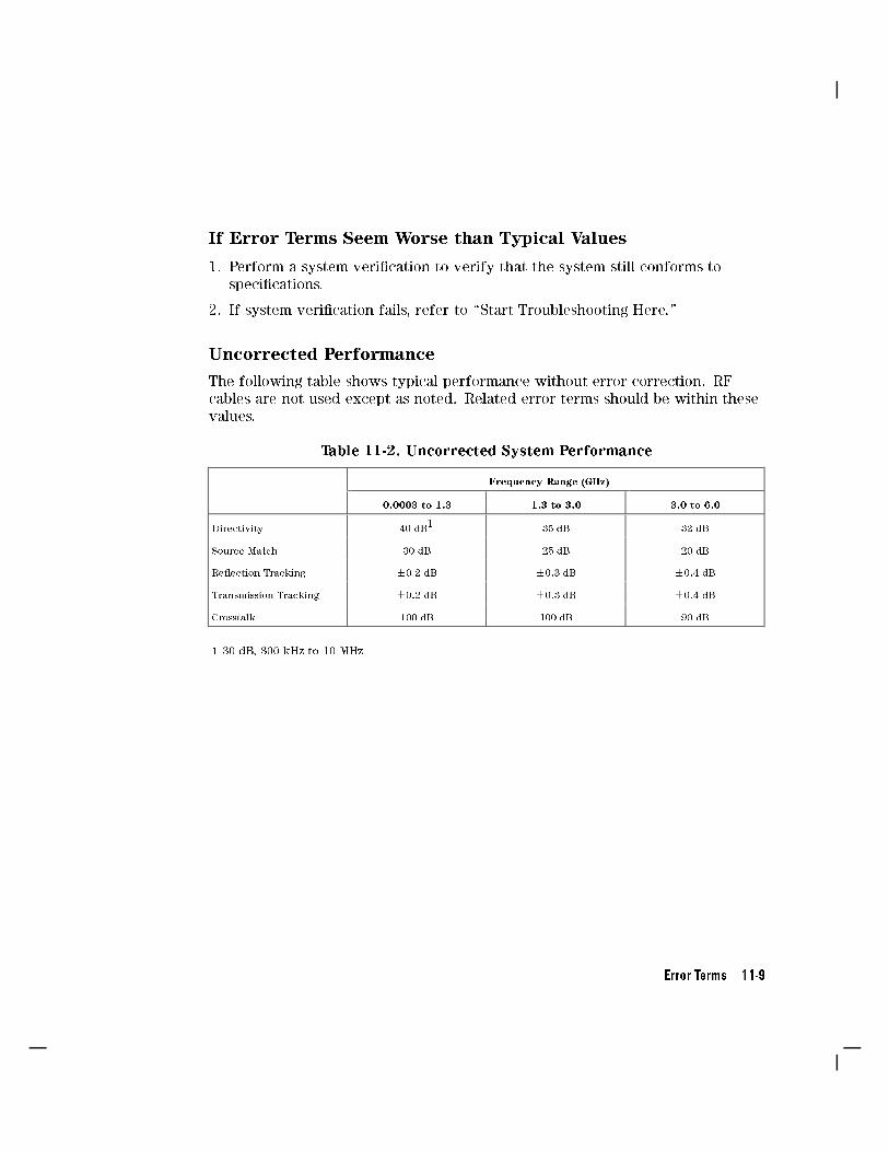
If Error Terms Seem Worse than Typical Values
1. Perform a system veri�cation to verify that the system still conforms tospeci�cations.
2. If system veri�cation fails, refer to \Start Troubleshooting Here."
Uncorrected Performance
The following table shows typical performance without error-correction. RFcables are not used except as noted. Related error terms should be within thesevalues.
Table 11-2. Uncorrected System Performance
Frequency Range (GHz)
0.0003 to 1.3 1.3 to 3.0 3.0 to 6.0
Directivity 40 dB1 35 dB 32 dB
Source Match 30 dB 25 dB 20 dB
Re ection Tracking �0.2 dB �0.3 dB �0.4 dB
Transmission Tracking �0.2 dB �0.3 dB �0.4 dB
Crosstalk 100 dB 100 dB 90 dB
1 30 dB, 300 kHz to 10 MHz
Error Terms 11-9

Error Term Descriptions
The error term descriptions in this section include the following information:
signi�cance of each error termtypical results following either a re ection 1-port or a response and isolationcalibrationguidelines to interpret each error term
11-10 Error Terms

Directivity (ED) - After a Re ection 1-Port Calibration
Description
Directivity is a measure of any detected power that is re ected when a load isattached to the test port. The directivity error of the test port is determined bymeasuring the re ection of the load during the error-correction procedure.
Signi�cant System Components
load used in the error-correction (calibration)test port connectorsanalyzer's directional coupler
A�ected Measurements
Low re ection device measurements are most a�ected by directivity errors.
Highly re ective device measurements will look normal.
Procedure
To view the analyzer's directivity parameters, perform a 1-port calibration, then
press: �SYSTEM�NNNNNNNNNNNNNNNNNNNNNNNNNNNNNNNNNNNNNNSERVICE MENU
NNNNNNNNNNNNNNTEST �32� �x1�.
Error Terms 11-11

Figure 11-4. Typical ED (Re ection Test Port)
11-12 Error Terms

Source Match (ES) - After a Re ection 1-Port Calibration
Description
Source match is a measure of test port connector match, as well as the matchbetween all components from the source to the test port. It is obtained bymeasuring the re ection of an open and a short connected directly to the testport.
Signi�cant System Components
open calibration kit deviceshort calibration kit deviceanalyzer's directional couplertest port connectors
A�ected Measurements
Re ection and transmission measurements of highly re ective devices are mosta�ected by source match errors.
Procedure
To view the analyzer's source match parameters, perform a 1-port calibration,
then press: �SYSTEM�NNNNNNNNNNNNNNNNNNNNNNNNNNNNNNNNNNNNNNSERVICE MENU
NNNNNNNNNNNNNNTEST �33� �x1�.
Error Terms 11-13

Figure 11-5. Typical ES (Re ection Test Port)
11-14 Error Terms

Re ection Tracking (ER) - After a Re ection 1-Port Calibration
Description
Re ection tracking is the di�erence between the frequency response of thereference path (R path) and the frequency response of the re ection test path(A input path). The error term is obtained by measuring the re ections of anopen and a short during calibration.
Signi�cant System Components
open calibration kit deviceshort calibration kit deviceR or A signal path for large variation in ER
A�ected Measurements
All re ection measurements (high or low return loss) are a�ected by there ection tracking errors.
Procedure
To view the analyzer's re ection tracking parameters, perform a 1- port
calibration, then press: �SYSTEM�NNNNNNNNNNNNNNNNNNNNNNNNNNNNNNNNNNNNNNSERVICE MENU
NNNNNNNNNNNNNNTEST �34� �x1�.
Error Terms 11-15
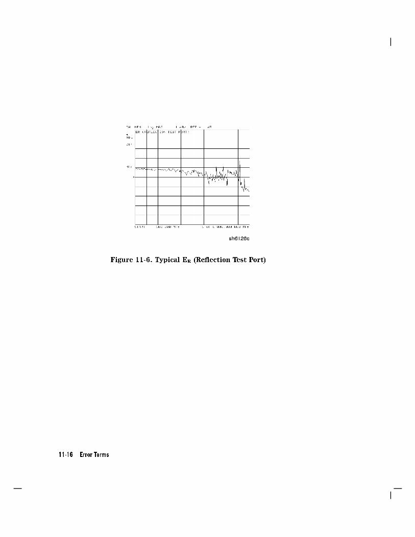
Figure 11-6. Typical ER (Re ection Test Port)
11-16 Error Terms

Isolation (Crosstalk, EX) - After a Response and Isolation(Transmission) Calibration
Description
Isolation is a measure of the leakage between the test ports and the signalpaths. The isolation error terms are characterized by measuring transmissionwith loads attached to both ports during the error-correction procedure. Sincethese terms are low in magnitude, they are usually noisy (not very repeatable).The error term magnitude changes dramatically with IF bandwidth: a 10 Hz IFbandwidth must be used in order to lower the noise oor beyond the crosstalkspeci�cation. Using averaging will also reduce the peak-to-peak noise in thiserror term.
Signi�cant System Components
sampler crosstalks
A�ected Measurements
Transmission measurements, (primarily where the measured signal level is verylow), are a�ected by isolation errors. For example, transmission measurements
where the insertion loss of the device under test is large.
Procedure
To view the analyzer's isolation parameters, perform a response and isolation
calibration, then press: �SYSTEM�NNNNNNNNNNNNNNNNNNNNNNNNNNNNNNNNNNNNNNSERVICE MENU
NNNNNNNNNNNNNNTEST �34� �x1�.
Error Terms 11-17

Figure 11-7. Typical EX with 10 Hz Bandwidth
Figure 11-8. Typical EX with 3 kHz Bandwidth
11-18 Error Terms

Transmission Tracking (ET)
Description
Transmission tracking is the di�erence between the frequency response of thereference path (including R input) and the transmission test path (including Ainput) while measuring transmission. The response of the test port cables isincluded. These terms are characterized by measuring the transmission of the
\thru" con�guration during the error-correction procedure.
Signi�cant System Components
R signal pathA input paths\thru" cable
A�ected Measurements
All transmission measurements are a�ected by transmission tracking errors.
Procedure
To view the analyzer's transmission tracking parameters, perform a 1-port
calibration, then press: �SYSTEM�NNNNNNNNNNNNNNNNNNNNNNNNNNNNNNNNNNNNNNSERVICE MENU
NNNNNNNNNNNNNNTEST �34� �x1�.
Error Terms 11-19

Figure 11-9. Typical ET
11-20 Error Terms

12
Theory of Operation
This chapter is divided into two major sections:
\How the HP 8752C Works" gives a general description of the HP 8752Cnetwork analyzer's operation.
\A Close Look at the Analyzer's Functional Groups" provides more detailedoperating theory for each of the analyzer's functional groups.
Theory of Operation 12-1

How the HP 8752C Works
Network analyzers measure the re ection and transmission characteristics ofdevices and networks. A network analyzer test system consists of the following:
source
signal-separation devices
receiver
display
The analyzer applies a signal that is either transmitted through the device undertest or re ected from its input, and then compares it with the incident signalgenerated by the swept RF source. These signals are then applied to a receiver
for measurement, signal processing, and display.
The HP 8752C vector network analyzer integrates a high resolution synthesizedRF source, transmission/re ection test set, and a dual channel three-input
receiver to measure and display magnitude, phase, and group delay of
transmitted and re ected power. The HP 8752C Option 010 has the additional
capability of transforming measured data from frequency domain to time
domain. Figure 12-1 is a simpli�ed block diagram of the network analyzersystem. A detailed block diagram of the analyzer is located at the end of the\Start Troubleshooting Here" chapter.
Figure 12-1. Simpli�ed Block Diagram of the Network Analyzer System
12-2 Theory of Operation

The Built-In Synthesized Source
The analyzer's built-in synthesized source produces a swept RF signal in therange of 300 kHz to 1.3 GHz. The HP 8752C Option 003 is able to generatesignals up to 3 GHz and the Option 006 generates signals up to 6 GHz. Thesource output power is leveled by an internal ALC (automatic leveling control)circuit. To achieve frequency accuracy and phase measuring capability, theanalyzer is phase locked to a highly stable crystal oscillator.
For this purpose, a portion of the transmitted signal is routed to the R
sampler/mixer of the receiver, where it is sampled by the phase detection loopand fed back to the source.
The Source Step Attenuator (Option 004)
The HP 8752C Option 004 includes a 70 dB, electro-mechanical step attenuator.
This very low-loss attenuator is contained in the source assembly. It is used to
adjust the power level to the device under test without changing the level ofthe incident power in the reference path. The user sets the attenuation levelsvia the front panel softkeys.
Theory of Operation 12-3

The Built-In Transmission/Re ection Test Set
The HP 8752C features a built-in test set that provides the signal separationcapability for the device under test. The test uses a dual directional couplerto separate the incident signal from the transmitted and re ected signals. Theincident signal is applied to the R sampler/mixer via one of coupled arms of thedual directional coupler. Meanwhile, the re ected signal is routed from there ection test port via the other coupled arm of the dual directional couplerto the input of the A sampler/mixer in the receiver. The transmitted signal is
fed directly from the transmission test port to the B sampler/mixer. (Analyzershaving Option 006 have an 8 dB pad between the transmission test port and theB sampler/mixer.)
The Receiver Block
The receiver block contains three sampler/mixers (for the R, A, and Binputs). The signals are sampled and down-converted to produce a 4 kHz IF(intermediate frequency). A multiplexer sequentially directs each of the threeIF signals to the ADC (analog to digital converter) where it is converted froman analog to a digital signal to be measured and processed for viewing on thedisplay. Both amplitude and phase information are measured simultaneously,regardless of what is displayed on the analyzer.
The Microprocessor
A microprocessor takes the raw data and performs all the required error
correction, trace math, formatting, scaling, averaging, and marker operationsaccording to the instructions from the front panel or over HP-IB. The formatted
data is then displayed.
12-4 Theory of Operation

A Close Look at the Analyzer's Functional Groups
The operation of the analyzer can be divided into �ve functional groups. Eachgroup consists of several major assemblies and performs a distinct function.Some assemblies are related to more than one group, and in fact all the groupsare to some extent interrelated and a�ect each other's performance.
Power Supply. The power supply functional group consists of the A8 postregulator and the A15 preregulator. It supplies power to the other assembliesin the instrument.
Digital Control. The digital control group consists of the A1 front panel andA2 front panel processor, the A9 CPU, the A16 rear panel, the A18 display,and the A19 graphics system processor (GSP) assemblies. The A10 digital IF
assembly is also related to this group. These assemblies combine to provide
digital control for the analyzer.
Source. The source group consists of the A3 source, A7 pulse generator, A11
phase lock, A12 reference, A13 fractional-N (analog), and A14 fractional-N
(digital) assemblies. The A4 R sampler is also related since it is part of the
source phase lock loop. The source supplies a phase-locked RF signal to the
device under test.
Signal Separation. The signal separation group consists of the A30 dual
directional coupler assembly. This assembly performs the function of a
re ection/transmission test set. It divides the source signal into a reference
path and a test path, and provides connections to the device under test.
Receiver. The receiver group consists of the A4/A5/A6 sampler/mixers andthe A10 digital IF assemblies. The A12 reference assembly and the A9 CPU
assembly are also related. The receiver measures and processes input signals
for display.
The following pages describe the operation of each of the functional groups.
Theory of Operation 12-5

Power Supply Theory
The power supply functional group consists of the A15 preregulator and theA8 post regulator. These two assemblies comprise a switching power supplythat provides regulated DC voltages to power all assemblies in the analyzer. TheA15 preregulator is enclosed in a casting at the rear of the instrument behindthe display. It is connected to the A8 post regulator by a wire bus (A15W1).Figure 12-2 is a simpli�ed block diagram of the power supply group.
Figure 12-2. Power Supply Functional Group, Simpli�ed Block Diagram
A15 Preregulator
The A15 preregulator steps down and recti�es the line voltage. It provides a
fully regulated +5V digital supply, and several preregulated voltages that go to
the A8 post regulator assembly for additional regulation.
The A15 preregulator assembly includes the line power module, a 60 kHz
switching preregulator, and overvoltage protection for the +5V digital supply. Itprovides LEDs (visible from the rear of the instrument) to indicate either normaloperating or shutdown status.
12-6 Theory of Operation

Line Power Module
The line power module includes the line power switch, voltage selector switch,and main fuse. The line power switch is activated from the front panel. Thevoltage selector switch, accessible at the rear panel, adapts the analyzer to localline voltages of approximately 115V or 230V (with 350 VA maximum). The mainfuse, which protects the input side of the preregulator against drawing excessiveline current, is also accessible at the rear panel. Refer to the HP 8752C Network
Analyzer Installation and Quick Start Guide for line voltage tolerances andother power considerations.
Preregulated Voltages
The switching preregulator converts the line voltage to several DC voltages.
The regulated +5V digital supply is routed directly to the motherboard. Thefollowing partially regulated voltages are routed through A15W1 to the A8 postregulator for �nal regulation:
+70V +25V +18V �18V +8V �8V
Regulated +5V Digital Supply
The +5VD supply is regulated by the control circuitry in the A15 preregulator.It is routed directly to the motherboard, and from there to all assembliesrequiring a low noise digital supply. A +5V sense line returns from the
motherboard to the A15 preregulator. The +5V CPU is derived from the +5 VD
in the A8 post regulator and goes directly to the A19 GSP.
In order for the preregulator to function, the +5V digital supply must be loadedby one or more assemblies, and the +5V sense line must be working. If not, the
other preregulated voltages will not be correct.
Shutdown Indications: the Green LED and Red LED
The green LED is on in normal operation. It is o� when line power is notconnected, not switched on, set too low, or if the line fuse has blown.
The red LED, which is o� in normal operation, lights to indicate a fault in the
+5V supply. This may be an over/under line voltage, over line current, or
overtemperature condition. Refer to the troubleshooting chapters for moreinformation.
Theory of Operation 12-7

A8 Post Regulator
The A8 post regulator �lters and regulates the DC voltages received from theA15 preregulator. It provides fusing and shutdown circuitry for individualvoltage supplies. It distributes regulated constant voltages to the individualassemblies throughout the instrument. It includes the overtemperatureshutdown circuit, the variable fan speed circuit, and the air ow detector. Ninegreen LEDs provide status indications for the individual voltage supplies.
Refer to the \Power Supply Block Diagram" located at the end of the \Power
Supply Troubleshooting" chapter to see the voltages provided by the A8 post
regulator.
Voltage Indications: the Green LEDs
The nine green LEDs along the top edge of the A8 assembly are on in normaloperation, to indicate the correct voltage is present in each supply. If they are
o� or ashing, a problem is indicated. The troubleshooting procedures later inthis chapter detail the steps to trace the cause of the problem.
Shutdown Circuit
The shutdown circuit is triggered by overcurrent, overvoltage, undervoltage, or
overtemperature. It protects the instrument by causing the regulated voltagesupplies to be shut down. It also sends status messages to the A9 CPU to triggerwarning messages on the analyzer's display. The voltages that are not shut
down are the +5VD and +5VCPU digital supplies from the preregulator, the
fan supplies, the probe power supplies, and the display supplies. The shutdown
circuit can be disabled momentarily for troubleshooting purposes by jumperingthe SDIS line (A8TP4) to ground.
Variable Fan Circuit and Air Flow Detector
The fan power is derived directly from the +18V and �18V supplies from theA15 preregulator. Because the fan is not fused, it will continue to provideair ow and cooling when the instrument is otherwise disabled. If overheatingoccurs, the main instrument supplies are shut down and the fan runs at full
speed. An overtemperature status message is sent to the A9 CPU to initiate awarning message on the analyzer's display. The fan also runs at full speed if the
air ow detector senses a low output of air from the fan. (Full speed is normal
at initial power on.)
12-8 Theory of Operation

Display Power
The A8 assembly supplies voltages to the display through a wire cable. The A8supplies +5VCPU and +65V to the A19 GSP, then the +65V is routed to thedisplay. Because they are not connected to the protective shutdown circuitry,the A18 display assemblies can operate during troubleshooting when othersupplies do not work.
Probe Power
The +18V and �18V supplies are post regulated to +15V and �12.6V to providea power source at the front panel for an external RF probe or milli-metermodules.
Digital Control Theory
The digital control functional group consists of the following assemblies:
A1 front panel
A2 front panel processor
A9 CPU
A10 digital IF
A16 rear panel
A18 display
A19 GSP
These assemblies combine to provide digital control for the entire analyzer.
They provide math processing functions, as well as communications between theanalyzer and an external controller and/or peripherals. Figure 12-3 is a blockdiagram of the digital control functional group.
Theory of Operation 12-9

Figure 12-3. Digital Control Group, Block Diagram
A1 Front Panel Keyboard
The A1 front panel keyboard assembly provides user interface with theanalyzer. It includes the keyboard for local user inputs, and the front panelLEDs that indicate instrument status. The RPG (rotary pulse generator) is not
electrically connected to the A1 front panel keyboard, but provides user inputs
directly to the front panel processor.
12-10 Theory of Operation

A2 Front Panel Processor
The A2 front panel processor detects and decodes user inputs from the frontpanel keys and RPG knob, and transmits them to the CPU. It has the capabilityto interrupt the CPU to provide information updates. It also controls the frontpanel LEDs that provide status information to the user.
A9 CPU/A10 Digital IF
The A9 CPU assembly contains the main CPU (central processing unit), thedigital signal processor, memory storage. The main CPU is the master controllerfor the analyzer, including the other dedicated microprocessors. The memoryincludes EEPROM, RAM, EPROM, and ROM.
Data from the receiver is serially clocked into the A9 CPU assembly fromthe A10 digital IF. The data-taking sequence is triggered either from the A14
fractional-N assembly, externally from the rear panel, or by �rmware on the A9
assembly.
Main CPU
The main CPU is a 16-bit microprocessor that maintains digital control over theentire instrument through the instrument bus. The main CPU receives external
control information from the front panel or HP-IB, and performs processing
and formatting operations on the raw data in the main RAM. It controls the
digital signal processor, the front panel processor, the display processor, andthe interconnect port interfaces. In addition, when the analyzer is in the
system controller mode, the main CPU controls peripheral devices through the
peripheral port interfaces.
The main CPU has a dedicated EPROM that contains the operating system
for instrument control. Front panel settings are stored in CMOS RAM, with abattery providing at least 5 years of backup storage when external power isswitched o�.
Main RAM
The main RAM (random access memory) is shared memory for the CPU andthe digital signal processor. It stores the raw data received from the digital
signal processor, while additional calculations are performed on it by the CPU.
The CPU reads the resulting formatted data from the main RAM and converts
it to GSP commands. It writes these commands to the GSP for output to the
analyzer's display.
Theory of Operation 12-11

Detailed information on the data processing sequence is provided in HP 8752CNetwork Analyzer User's Guide.
EEPROM
EEPROM (electrically-erasable programmable read only memory) containsfactory set correction constants unique to each instrument. These constantscorrect for hardware variations to maintain the highest measurement accuracy.
The correction constants can be updated by executing the routines in the
\Adjustments and Correction Constants" chapter.
Digital Signal Processor
The digital signal processor receives the digitized data from the A10 digitalIF. It computes discrete Fourier transforms to extract the complex phase and
magnitude data from the 4 kHz IF signal. The resulting raw data is written intothe main RAM.
A18 Display
The A18 display is a 7.5-inch raster scan CRT with associated drive circuitry.
It receives a +65V power supply from the A19 GSP, along with digital TTL
horizontal and vertical sync signals, as well as red, green, and blue (RGB)
video signals. Automatic degaussing is performed whenever the instrument isswitched on to minimize the magnetization of the display.
A19 GSP
The A19 graphics system processor (GSP) provides an interface between theA9 CPU and the A18 display. The CPU (A9) converts the formatted data toGSP commands and writes it to the GSP. The GSP processes the data to obtain
the necessary video signals and sends the signals to the A18 display. It alsoproduces RGB output signals which are sent to the rear panel. The assemblyreceives two power supply voltages: +5VCPU, which is used for processing, and+65V, which is passed on to A18 display but not used on A19 GSP.
12-12 Theory of Operation

A16 Rear Panel
The A16 rear panel includes the following interfaces:
TEST SET I/O INTERCONNECT. The HP 8752C cannot be used with externaltest sets. However, with an adapter, you can use signal levels for sequencing.Refer to the \Application and Operation Concepts" chapter of the HP 8752CNetwork Analyzer User's Guide for information on applying the test setinterconnect.
EXT REF IN. This allows for a frequency reference signal input that canphase lock the analyzer to an external frequency standard for increasedfrequency accuracy.
The analyzer automatically enables the external frequency reference featurewhen a signal is connected to this input. When the signal is removed, theanalyzer automatically switches back to its internal frequency reference.
AUX INPUT. This allows for a dc or ac voltage input from an external signalsource, such as a detector or function generator, which you can then measure.
(You can also use this connector as an analog output in service routines.)
EXT AM. This allows an external analog signal input to be applied to the
ALC circuitry of the analyzer's source. This input analog signal amplitude
modulates the RF output signal.
EXT TRIGGER. This allows connection of an external negative
TTL-compatible signal that will trigger a measurement sweep. The trigger can
be set to external through softkey functions.
EXT MON: RED, GREEN, BLUE. Although these interfaces are notelectrically connected to the A16 rear panel interface board, they areconnected to the rear panel assembly. Three video output connectorsprovide analog blue, green, and red video signals which you can use todrive an analog multi-sync monitor. The monitor must be compatible withthe analyzer's 25.5 kHz scan rate and video levels: 1 Vp-p, 0.7 V=white,0 V=black, �0.3 V sync, sync on green.
Theory of Operation 12-13

Source Theory Overview
The source produces a highly stable and accurate RF output signal by phaselocking a YIG oscillator to a harmonic of the synthesized VCO (voltage controlledoscillator). The source output produces a CW or swept signal between 300 kHzand 1.3 GHz (3 GHz for Option 003 and 6 GHz for Option 006). The maximumleveled power is +5 dBm. Option 004 analyzers have a 70 dB step attenuatorbuilt into the source that allows the power to be decreased to �85 dBm andincreased to a maximum leveled power of +10 dBm.
The full frequency range of the source is produced in 13 subsweeps, two in lowband and eleven in high band. The high band frequencies start at 16 MHz andgo up to 1.3 GHz (3 GHz for Option 003 and 6 GHz for Option 006). The highband frequencies are achieved by harmonic mixing with a di�erent harmonicnumber for each subsweep. The low band frequencies (300 kHz to 16 MHz) are
down-converted by fundamental mixing.
The source functional group consists of the individual assemblies describedbelow.
A14/A13 Fractional-N
These two assemblies comprise the synthesizer. The 30 to 60 MHz VCO in
the A14 assembly generates the stable LO frequencies for fundamental andharmonic mixing.
A12 Reference
This assembly provides stable reference frequencies to the rest of theinstrument by dividing down the output of a 40 MHz crystal oscillator. In lowband operation, the output of the fractional-N synthesizer is mixed down in theA12 reference assembly. (The 2nd LO signal from the A12 assembly is explainedin \Receiver Theory".)
A7 Pulse Generator
A step recovery diode in the pulse generator produces a comb of harmonicmultiples of the VCO output. These harmonics provide the high band LO (local
oscillator) input to the samplers. In low band operation the pulse generator is
turned o�.
12-14 Theory of Operation

A11 Phase Lock
This assembly compares the �rst IF (derived from the source output in the A4 Rsampler) to a stable reference, and generates an error voltage that is integratedinto the drive for the A3 source assembly.
A3 Source
This assembly includes a 3.0 to 6.8 GHz YIG oscillator and a 3.8 GHz cavityoscillator. The outputs of these oscillators are mixed to produce the RF outputsignal. In Option 006 (300 kHz to 6 GHz) the frequencies 3.0 to 6.0 GHz are nolonger a mixed product, but are the direct output of the YIG oscillator. Thesignal tracks the stable output of the synthesizer. The ALC (automatic leveling
control) circuitry is also in the A3 assembly.
Theory of Operation 12-15
Source Low Band Operation
The low band frequency range is 300 kHz to 16 MHz. These frequencies aregenerated by locking the A3 source to a reference signal. The reference signalis synthesized by mixing down the fundamental output of the fractional-N VCOwith a 40 MHz crystal reference signal. Low band operation di�ers from highband in these respects: The reference frequency for the A11 phase lock is not a�xed 1 MHz signal, but varies with the frequency of the fractional-N VCO signal.The sampler diodes are biased on to pass the signal through to the mixer. The1st IF signal from the A4 R sampler is not �xed but is identical to the sourceoutput signal and sweeps with it. The following steps outline the low bandsweep sequence, illustrated in Figure 12-4.
1. A signal (FN LO) is generated by the fractional-N VCO. The VCO in the
A14 fractional-N assembly generates a CW or swept signal that is 4O MHzgreater than the start frequency. The signal is divided down to 1OO kHz andphase locked in the A13 assembly, as in high band operation.
2. The fractional-N VCO signal is mixed with 40 MHz to produce a
reference signal. The signal (FN LO) from the fractional-N VCO goes to the
A12 reference assembly, where it is mixed with the 4O MHz VCXO (voltage
controlled crystal oscillator). The resulting signal is the reference to thephase comparator in the A11 assembly.
3. The A3 source is pretuned. The source output is fed to the A4 R
sampler/mixer. The pretuned DAC in the A11 phase lock assembly sets
the A3 source to a frequency 1 to 6 MHz above the start frequency. This
signal (source output) is applied to the A4 R sampler/mixer assembly via thecoupled arm of the A30 dual directional coupler.
4. The signal from the source is fed back (1st IF) to the phase comparator.The source output signal passes directly through the R sampler in the A4assembly, because the sampler is biased on. The signal (1st IF) is fed backunaltered to the phase comparator in the A11 phase lock assembly. The otherinput to the phase comparator is the heterodyned reference signal from theA12 assembly. Any frequency di�erence between these two signals producesa proportional error voltage.
5. A tuning signal (YO DRIVE) tunes the source and phase lock is achieved.The error voltage is used to drive the A3 source YIG oscillator to bring theYIG closer to the reference frequency. The loop process continues until the
source frequency and the reference frequency are the same and phase lock is
achieved.
12-16 Theory of Operation

6. A synthesized sub sweep is generated. The source tracks thesynthesizer. When phase lock is achieved at the start frequency, thesynthesizer starts to sweep. This changes the phase lock reference frequencyand causes the source to track at a di�erence frequency 40 MHz below thesynthesizer.
Figure 12-4. Low Band Operation of the Source
Theory of Operation 12-17

The full low band is produced in two subsweeps, to allow addition IF �lteringbelow 3 MHz . At the transition between subsweeps, the source is pretunedand then relocks. Table 12-1 lists the low band subsweep frequencies at thefractional-N VCO and the source output.
Table 12-1. Low Band Subsweep Frequencies
Fractional-N (MHz) 1st IF (MHz) Source Output (MHz)
40.3 to 43.3 0.3 to 3.3 0.3 to 3.3
43.3 to 56.0 3.3 to 16.0 3.3 to 16.0
12-18 Theory of Operation

Source High Band Operation
The high band frequency range is 16 MHz to 1.3 GHz (3.0 GHz for Option 003and 6.0 GHz for Option 006). These frequencies are generated in subsweeps byphase-locking the A3 source signal to harmonic multiples of the fractional-NVCO. The high band subsweep sequence, illustrated in Figure 12-5, follows thesesteps:
1. A signal (HI OUT) is generated by the fractional-N VCO. The VCO in theA14 fractional-N assembly generates a CW or swept signal in the range of3O to 6O MHz. This signal is synthesized and phase locked to a 1OO kHzreference signal from the A12 reference assembly. The signal from thefractional-N VCO is divided by 1 or 2, and goes to the pulse generator.
2. A comb of harmonics (1st LO) is produced in the A7 pulse generator.
The divided-down signal from the fractional-N VCO drives a step recovery
diode (SRD) in the A7 pulse generator assembly. The SRD multipliesthe fundamental signal from the fractional-N into a comb of harmonicfrequencies. The harmonics are used as the 1st LO (local oscillator) signal to
the samplers. One of the harmonic signals is 1 MHz below the start signal set
from the front panel.
3. The A3 source is pretuned. The source output is fed to the A4 R
sample/mixer. The pretune DAC in the A11 phase lock assembly sets the A3
source to a �rst approximation frequency (1 to 6 MHz higher than the start
frequency). This signal (RF OUT) goes to the A4 R sampler/mixer assembly
via the coupled arm of the dual directional coupler.
4. The synthesizer signal and the source signal are combined by thesampler. A di�erence frequency is generated. In the A4 R sampler, the 1st
LO signal from the pulse generator is combined with the source output signal.The IF (intermediate frequency) produced is a �rst approximation of 1 MHz.The 1st IF is routed back to the A11 phase lock assembly.
5. The di�erence frequency (1st IF) from the A4 R sampler is compared toa reference. The 1st IF feedback signal from the A4 is �ltered and applied to
a phase comparator circuit in the A11 phase lock assembly. The other input
to the phase comparator is a crystal-controlled 1 MHz signal from the A12reference assembly. Any frequency di�erence between these two signals
produces a proportional error voltage.
Theory of Operation 12-19

6. A tuning signal (YO DRIVE) tunes the source and phase lock is achieved.The error voltage is used to drive the A3 source YIG oscillator, in order tobring it closer to the required frequency. The loop process continues untilthe 1st IF feedback signal to the phase comparator is equal to the 1 MHzreference signal, and phase lock is achieved.
7. A synthesized subsweep is generated by A13/A14. The A3 source tracksthe synthesizer. When the source is phase locked to the synthesizer at thestart frequency, the synthesizer starts to sweep. The phase locked loop forcesthe source to track the synthesizer, maintaining a constant 1 MHz 1st IFsignal.
The full high band sweep is generated in a series of subsweeps, by phaselocking the A3 source signal to harmonic multiples of the fractional-N VCO.
The 16 to 31 MHz subsweep is produced by a one-half harmonic, using
the divide-by-2 circuit on the A14 assembly. At the transitions between
subsweeps, the source is pretuned and then relocks. Table 12-2 lists the highband subsweep frequencies from the fractional-N VCO and the source output.
12-20 Theory of Operation

Figure 12-5. High Band Operation of the Source
Theory of Operation 12-21

Table 12-2. High Band Subsweep Frequencies
Fractional-N (MHz) Harmonic Source Output (MHz)
30 to 60 1/2 16 to 31
30 to 60 1 31 to 61
30 to 60 2 61 to 121
40 to 59 3 121 to 178
35.4 to 59.2 5 178 to 296
32.8 to 59.4 9 296 to 536
35.7 to 59.5 15 536 to 893
33.0 to 59.5 27 893 to 1607
31.5 to 58.8 51 1607 to 3000
37.0 to 59.6 83 3000 to 4950
49.0 to 59.4 101 4950 to 6000
12-22 Theory of Operation

Signal Separation
The A30 Dual Directional Coupler
Signal separation in the analyzer is accomplished with a dual directional couplerwhich, by itself, comprises the analyzer's built-in test set. The dual directionalcoupler is connected to the re ection test port. It is used to separate theincident signal going to the device under test from re ected signal coming fromthe device under test. The incident signal is applied to the R sampler/mixer viaone of coupled arms of the dual directional coupler. Meanwhile, the re ectedsignal is routed from the re ection test port via the other coupled arm of thedual directional coupler to the input of the A sampler/mixer in the receiver.
The transmitted signal is fed directly from the transmission test port to the Bsampler/mixer. (Analyzers having Option 006 have an 8 dB pad between the
transmission test port and the B sampler/mixer.)
Receiver Theory
The receiver functional group consists of the following assemblies:
A4 R sampler/mixer
A5 A sampler/mixer
A6 B sampler/mixer
A10 digital IF
These assemblies combine with the A9 CPU (described in \Digital ControlTheory") to measure and process input signals into digital information fordisplay on the analyzer. Figure 12-6 through Figure 12-9 are simpli�ed blockdiagrams of the di�erent receiver functional groups for the various analyzeroptions.
Theory of Operation 12-23

Figure 12-6. Receiver Functional Group (standard and Option 003)
12-24 Theory of Operation

Figure 12-7. Receiver Functional Group (Option 003 and 004)
Theory of Operation 12-25

Figure 12-8. Receiver Functional Group (Option 006)
12-26 Theory of Operation

Figure 12-9. Receiver Functional Group (Option 004 and 006)
Theory of Operation 12-27

A4/A5/A6 Sampler/Mixer
The A4, A5, and A6 sampler/mixers all down-convert the RF input signals to�xed 4 kHz 2nd IF signals with amplitude and phase corresponding to the RFinput. For the analyzer with with Option 006, the A6 B sampler/mixer assemblyincludes an 8 dB gain preampli�er in front of the sampler. This improves thenoise �gure performance of the analyzer's receiver channel B.
The Sampler Circuit in High Band
In high band operation, the sampling rate of the samplers is controlled bythe 1st LO from the A7 pulse generator assembly. The 1st LO is a comb ofharmonics produced by a step recovery diode driven by the fractional-N VCOfundamental signal. One of the harmonic signals is 1 MHz below the startfrequency set at the front panel. The 1st LO is combined in the samplers withthe source output signal. In options 003 and 006, samplers are additionallycapable of receiving RF input signals up to 3 and 6 GHz respectively. The mixing
products are �ltered, so that the only remaining response is the di�erencebetween the source frequency and the harmonic 1 MHz below it. This �xed1 MHz signal is the 1st IF. Part of the 1st IF signal from the A4 R sampler is fed
back to the A11 phase lock assembly.
The Sampler Circuit in Low Band
In low band the sampler diodes are biased continuously on, so that the RF inputsignal passes through them unchanged. Thus the 1st IF is identical to the RFoutput signal from the source (300 kHz to 16 MHz), and sweeps with it. Part
of the 1st IF signal from the A4 R sampler is fed back to the A11 phase lockassembly.
(Refer to \Source Theory Overview" for information on high band and low bandoperation of the source.)
The 2nd LO Signal
The 2nd LO is obtained from the A12 reference assembly. In high band, the 2nd
LO is �xed at 996 kHz. This is produced by feeding the 39.84 MHz output of aphase-locked oscillator in the A12 assembly through a divide-by-40 circuit.
In low band, the 2nd LO is a variable frequency produced by mixing the outputof the fractional-N VCO with a �xed 39.996 MHz signal in the A12 assembly.The 2nd LO covers the range of 0.014 to 16.004 MHz in two subsweeps thatcorrespond with the source subsweeps. These subsweeps are 0.304 to 3.304 MHzand 3.304 to 16.004 MHz.
12-28 Theory of Operation

The Mixer Circuit
The 1st IF and the 2nd LO are combined in the mixer circuit. The resultingdi�erence frequency (the 2nd IF) is a constant 4 kHz in both bands, asTable 12-3 shows.
Table 12-3. Mixer Frequencies
Band 1st IF 2nd LO 2nd IF
Low 0.300 to 16.0 MHz 0.304 to 16.004 MHz 4.0 kHz
High 1.000 MHz 0.996 MHz 4.0 kHz
A10 Digital IF
The three 4 kHz 2nd IF signals from the sampler/mixer assemblies are inputto the A10 digital IF assembly. These signals are sampled at a 16 kHz rate. A
fourth input is the analog bus, which can monitor either an external input at
the rear panel AUX IN connector or one of 31 internal nodes. A multiplexer
sequentially directs each of the signals to the ADC (analog-to-digital converter).Here they are converted to digital form and sent to the A9 CPU assembly forprocessing. Refer to \Digital Control Theory" for more information on signalprocessing.
Theory of Operation 12-29


13
Replaceable Parts
This chapter contains information for ordering replacement parts for theHP 8752C network analyzer. Replaceable parts include the following:
major assemblies
cables
chassis hardware
In general, parts of major assemblies are not listed. Refer to \Abbreviations" atthe back of this chapter to help interpret part descriptions in the replaceableparts lists that follow.
Replaceable Parts 13-1

Assembly Replacement Sequence
The following steps show the sequence to replace an assembly in an HP 8752CNetwork Analyzer.
1. Identify the faulty group. Refer to the \Start Troubleshooting Here" chapter.Follow up with the appropriate troubleshooting chapter that identi�es thefaulty assembly.
2. Order a replacement assembly. Refer to the \Replaceable Parts" chapter.
3. Replace the faulty assembly and determine what adjustments are necessary.Refer to the \Assembly Replacement and Post-Repair Procedures" chapter.
4. Perform the necessary adjustments. Refer to the \Adjustments and
Correction Constants" chapter.
5. Perform the necessary performance tests. Refer to the \System Veri�cationand Performance Tests" chapter.
Save Money with Rebuilt-Exchange Assemblies
Under the rebuilt-exchange assembly program, certain factory-repaired andtested modules (assemblies) are available on a trade-in basis. These assemblies
cost less than a new assembly, and meet all factory speci�cations required of a
new assembly.
The defective assembly must be returned for credit under the terms of therebuilt-exchange assembly program. Figure 13-1 illustrates the module exchangeprocedure. \Major Assemblies" shows all major assemblies, including those thatcan be replaced on an exchange basis.
13-2 Replaceable Parts

Figure 13-1. Module Exchange Procedure
Replaceable Parts 13-3

Gather This Information Before Ordering
To order a part listed in the replaceable parts lists:
1. Determine the part number.2. Determine the quantity required.3. Mail this information to the nearest Hewlett-Packard o�ce or, in the U.S.,
call the hotline number listed in the following section.
To order a part not listed in the replaceable parts lists:
1. Note the instrument model number (HP 8752C).2. Note the serial number and options, if any (see rear panel).3. Describe the part.4. Describe the function of the part.5. Determine the quantity required.6. Mail this information to the nearest Hewlett-Packard o�ce or, in the U.S.,
call the hotline number listed in the following section.
Call (800) 227-8164 to Order Parts Fast (U.S. only)
When you have gathered the information required to place an order, contact
Hewlett-Packard's direct ordering team by calling the following toll-free hotline
number:
(800) 227-8164
Monday through Friday, 6 AM to 5 PM (Paci�c Standard Time)
The parts specialists have direct online access to replacement parts inventorycorresponding to the replaceable parts lists in this manual. Four day deliverytime is standard; there is a charge for hotline one-day delivery.
This information applies to the United States only. Outside the United States,contact your nearest HP o�ce.
13-4 Replaceable Parts

Replaceable Part Listings
The following pages list the replacement part numbers and descriptions forthe HP 8753C network analyzer. Illustrations with reference designatorsare provided to help identify and locate the part needed. The parts lists areorganized into the following categories:
Major Assemblies
Front Panel Assemblies
Rear Panel Assemblies
Cables, Top View
Front Panel, Cables and Attaching Hardware
Rear Panel, Cables and Attaching Hardware
Source and Sampler Parts: Standard and Option 003
Source and Sampler Parts: Option 004/006
Source and Sampler Parts: Options 004 and 003/004
Source and Sampler Parts: Option 006
Display Bezel Assembly
Chassis Parts
Top View of Attaching Hardware and Post Regulator Fuses
Bottom View of Attaching Hardware
Right View of Attaching Hardware
Left View of Attaching Hardware
Rear Panel Attaching Hardware
Replaceable Labels
Miscellaneous Parts and Accessories
Replaceable Parts 13-5
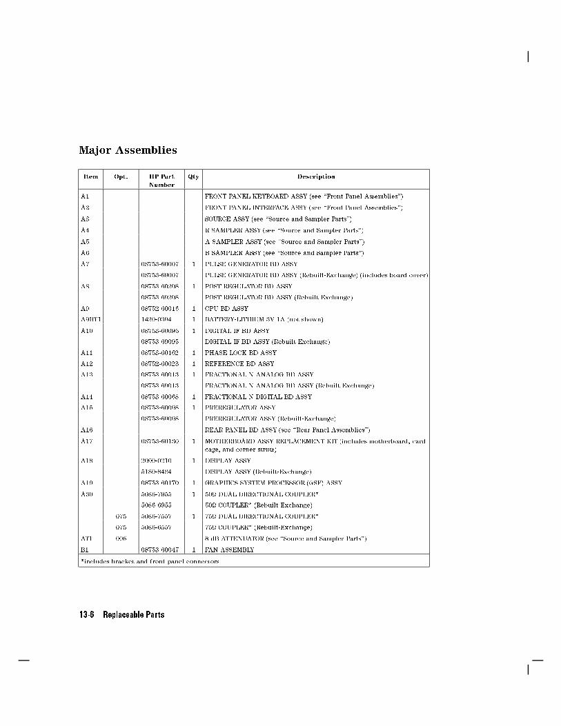
Major Assemblies
Item Opt. HP Part
Number
Qty Description
A1 FRONT PANEL KEYBOARD ASSY (see \Front Panel Assemblies")
A2 FRONT PANEL INTERFACE ASSY (see \Front Panel Assemblies")
A3 SOURCE ASSY (see \Source and Sampler Parts")
A4 R SAMPLER ASSY (see \Source and Sampler Parts")
A5 A SAMPLER ASSY (see \Source and Sampler Parts")
A6 B SAMPLER ASSY (see \Source and Sampler Parts")
A7 08753-60007 1 PULSE GENERATOR BD ASSY
08753-69007 PULSE GENERATOR BD ASSY (Rebuilt-Exchange) (includes board cover)
A8 08753-60208 1 POST REGULATOR BD ASSY
08753-69208 POST REGULATOR BD ASSY (Rebuilt-Exchange)
A9 08752-60016 1 CPU BD ASSY
A9BT1 1420-0394 1 BATTERY-LITHIUM 3V 1A (not shown)
A10 08753-60095 1 DIGITAL IF BD ASSY
08753-69095 DIGITAL IF BD ASSY (Rebuilt-Exchange)
A11 08753-60162 1 PHASE LOCK BD ASSY
A12 08752-60023 1 REFERENCE BD ASSY
A13 08753-60013 1 FRACTIONAL-N ANALOG BD ASSY
08753-69013 FRACTIONAL-N ANALOG BD ASSY (Rebuilt-Exchange)
A14 08753-60068 1 FRACTIONAL-N DIGITAL BD ASSY
A15 08753-60098 1 PREREGULATOR ASSY
08753-69098 PREREGULATOR ASSY (Rebuilt-Exchange)
A16 REAR PANEL BD ASSY (see \Rear Panel Assemblies")
A17 08753-60130 1 MOTHERBOARD ASSY REPLACEMENT KIT (includes motherboard, card
cage, and corner struts)
A18 2090-0210 1 DISPLAY ASSY
5180-8484 DISPLAY ASSY (Rebuilt-Exchange)
A19 08753-60170 1 GRAPHICS SYSTEM PROCESSOR (GSP) ASSY
A30 5086-7955 1 50 DUAL DIRECTIONAL COUPLER*
5086-6955 50 COUPLER* (Rebuilt-Exchange)
075 5086-7557 1 75 DUAL DIRECTIONAL COUPLER*
075 5086-6557 75 COUPLER* (Rebuilt-Exchange)
AT1 006 8 dB ATTENUATOR (see \Source and Sampler Parts")
B1 08753-60047 1 FAN ASSEMBLY
*includes bracket and front panel connectors
13-6 Replaceable Parts

Major Assemblies
Replaceable Parts 13-7

Front Panel Assemblies
Item Opt. HP Part
Number
Qty Description
1 08752-60029 1 50 FRONT DRESS PANEL
1 075 08752-60030 1 75 FRONT DRESS PANEL
2 2190-0016 3 WASHER-LOCK INTERNAL T 3/8 INCH 0.377-INCH-ID
3 2950-0043 3 NUT-HEX-DOUBLE CHAMFER 3/8-32-THREAD
4 01650-47401 1 RPG KNOB
5* 0515-0374 6 SCREW-MACHINE M3.0�10 CW-PN-TX
6 08752-40003 1 KEYPAD, RUBBER
7* 0515-1410 2 SCREW-MACHINE M3.0 � 20 CW-PN-TX
8* 0515-0375 2 SCREW-MACHINE M3.0 � 16 CW-PN-TX
A1 08753-60140 1 FRONT PANEL KEYBOARD ASSY
A1W1 RIBBON CA ASSY, A1 to A2 (p/o A1) (see \Cables, Top View")
A2 08753-60091 1 FRONT PANEL INTERFACE BD ASSY
RPG1 08757-60053 1 ROTARY PULSE GENERATOR (RPG)
W18 08711-60037 1 PROBE POWER CA ASSY, A2 to FRONT PANEL
*Metric hardware: other thread types will damage threaded holes.
13-8 Replaceable Parts

Front Panel Assemblies
Replaceable Parts 13-9

Rear Panel Assemblies
Item Opt. HP Part
Number
Qty Description
1 REAR FRAME (see \Chassis Parts")
2 2190-0584 4 WASHER-LOCK HELICAL 3.0 MM 3.1-MM-ID
3* 0515-0965 4 SCREW-SOCKET-HEAD-CAP M3 � 0.5 14MM-LONG
4 08753-20040 1 FAN GASKET
5 08753-00047 1 REAR PANEL
A16 08752-60013 1 REAR PANEL BD ASSY (includes A16W1)
B1 08753-60047 1 FAN (includes cable assembly)
W13 CA ASSY, REAR PANEL to A12 (see \Cables, Top View")
*Metric hardware: other thread types will damage threaded holes.
13-10 Replaceable Parts

Rear Panel Assemblies
Replaceable Parts 13-11

Cables, Top View
Item Opt. HP Part
Number
Qty Description
A18W1 p/o A18 1 CA ASSY, A18 to A19
W1 08752-20021 1 SEMI-RIGID CA ASSY, A3 to A30 (see \Front Panel, Cables and Attaching
Hardware")
W2 5021-8770 1 SEMI-RIGID CA ASSY, A30 to A4
W3 5021-8771 1 SEMI-RIGID CA ASSY, A30 to A5
W4 08753-20030 1 SEMI-RIGID CA ASSY, RF IN to A6
W5 08753-60027 1 FLX RF CA ASSY, A7 to A4
W6 08753-60027 1 FLX RF CA ASSY, A7 to A5
W7 08753-60027 1 FLX RF CA ASSY, A7 to A6
W8 08753-60061 1 FLX RF CA ASSY, A4 to A11
W9 08753-60061 1 FLX RF CA ASSY, A14 to A7
W10 08753-60029 1 FLX RF CA ASSY, A14 to A12
W11 08753-60029 1 FLX RF CA ASSY, A14 to A13
W12 08753-60029 1 FLX RF CA ASSY, A12 to A13
W13 08753-60026 1 FLX RF CA ASSY, A16 to A12
W14 08753-60113 1 DISPLAY POWER CA ASSY, A8 to A19
W20 08513-60036 1 CA ASSY, A9 to A19
13-12 Replaceable Parts

Cables, Top View
Replaceable Parts 13-13

Front Panel, Cables and Attaching Hardware
Item Opt. HP Part
Number
Qty Description
1* 0515-0458 3 SCREW-MACHINE M3.5�8 CW-PN-TX
W1 5021-8769 1 SEMI-RIGID CA ASSY, A3 to A30
W3 5021-8771 1 SEMI-RIGID CA ASSY, A30 to A5
W17 08753-60033 1 RIBBON CA ASSY, A2 to A17
W50 1250-2189 1 CA ASSY, A30 to REFLECTION PORT
W75 075 1250-2311 1 CA ASSY, A30 to REFLECTION PORT
*Metric hardware: other thread types will damage threaded holes.
Note The cables described on this page are common to all instrumentoptions. For option speci�c cables refer to the \Source and
Sampler Parts" section for your option.
13-14 Replaceable Parts

Front Panel Cables and Attaching Hardware
Replaceable Parts 13-15

Rear Panel, Cables and Attaching Hardware
Item Opt. HP Part
Number
Qty Description
1* 0515-0965 4 SCREW-MACHINE M3.0�14 SH-HX
2 2190-0584 4 WASHER-LOCK M3.0 NOM
A15W1 p/o A15 1 CA ASSY, A15 to A8 and A17
A16W1 08753-60033 1 RIBBON CA ASSY, A16 to A17 (p/o A16)
W13 08753-60026 1 FLX RF CA ASSY, REAR PANEL to A12
W21 08753-60117 1 FLX RF CA ASSY, RED (p/o A16)
W22 08753-60118 1 FLX RF CA ASSY, GREEN (p/o A16)
W23 08753-60119 1 FLX RF CA ASSY, BLUE (p/o A16)
*Metric hardware: other thread types will damage threaded holes.
13-16 Replaceable Parts

Rear Panel Cables and Attaching Hardware
Replaceable Parts 13-17

Source and Sampler Parts: Standard and Option 003
Item HP Part
Number
Qty Description
A3 08753-60234 1 SOURCE ASSY
A3 08753-69234 SOURCE ASSY (Rebuilt-Exchange)
A3MP1 1250-0590 1 SMB CAP
A3W1 08753-20107 1 RF CA, SEMI-RIGID, EYO (A3A3) to SOURCE (A3)
A3W2 08753-20032 1 RF CA, SEMI-RIGID, CAV OSC (A3A4) to SOURCE (A3)
A3A2W1 08753-60034 1 RIBBON CA ASSY, EYO (A3A3) to ALC (A3A2)
A3W7 08752-20024 1 RF CA, 4 dB ATTENUATOR (A3AT1) to BULKHEAD (A3 OUTPUT)
A4 08753-60004 1 R SAMPLER ASSY
A5 08753-60004 1 A SAMPLER ASSY
A6 08753-60004 1 B SAMPLER ASSY
W1 08752-20021 1 RF CA, SOURCE (A3) to COUPLER (A30)
W2 5021-8770 1 RF CA, COUPLER (A30) to R SAMPLER (A4)
W3 5021-8771 1 RF CA, COUPLER (A30) to A SAMPLER (A5)
W4 08753-20030 1 RF CA, TRANSMISSION PORT to B SAMPLER (A6)
13-18 Replaceable Parts

Source and Sampler Parts: Standard and Option 003
Replaceable Parts 13-19
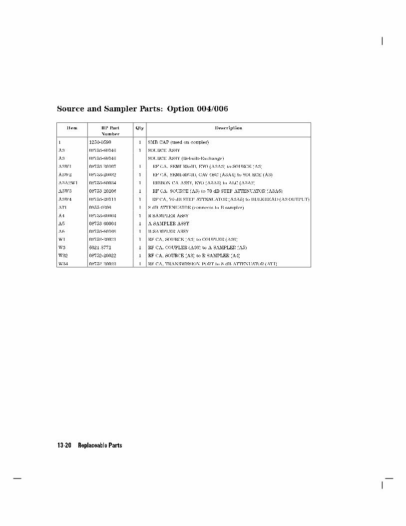
Source and Sampler Parts: Option 004/006
Item HP Part
Number
Qty Description
1 1250-0590 1 SMB CAP (used on coupler)
A3 08753-60146 1 SOURCE ASSY
A3 08753-69146 SOURCE ASSY (Rebuilt-Exchange)
A3W1 08753-20107 1 RF CA, SEMI-RIGID, EYO (A3A3) to SOURCE (A3)
A3W2 08753-20032 1 RF CA, SEMI-RIGID, CAV OSC (A3A4) to SOURCE (A3)
A3A2W1 08753-60034 1 RIBBON CA ASSY, EYO (A3A3) to ALC (A3A2)
A3W3 08753-20106 1 RF CA, SOURCE (A3) to 70 dB STEP ATTENUATOR (A3A5)
A3W4 08753-20111 1 RF CA, 70 dB STEP ATTENUATOR (A3A5) to BULKHEAD (A3 OUTPUT)
AT1 0955-0206 1 8 dB ATTENUATOR (connects to B sampler)
A4 08753-60004 1 R SAMPLER ASSY
A5 08753-60004 1 A SAMPLER ASSY
A6 08753-60169 1 B SAMPLER ASSY
W1 08752-20021 1 RF CA, SOURCE (A3) to COUPLER (A30)
W3 5021-8771 1 RF CA, COUPLER (A30) to A SAMPLER (A5)
W32 08752-20022 1 RF CA, SOURCE (A3) to R SAMPLER (A4)
W34 08752-20023 1 RF CA, TRANSMISSION PORT to 8 dB ATTENUATOR (AT1)
13-20 Replaceable Parts

Source and Sampler Parts: Option 004/006
Replaceable Parts 13-21

Source and Sampler Parts: Options 004 and 003/004
Item HP Part
Number
Qty Description
1 1250-0590 1 SMB CAP
A3 08753-60231 1 SOURCE ASSY
A3 08753-69231 SOURCE ASSY (Rebuilt-Exchange)
A3W1 08753-20107 1 RF CA, SEMI-RIGID, EYO (A3A3) to SOURCE (A3)
A3W2 08753-20032 1 RF CA, SEMI-RIGID, CAV OSC (A3A4) to SOURCE (A3)
A3A2W1 08753-60034 1 RIBBON CA ASSY, EYO (A3A3) to ALC (A3A2)
A3W3 08753-20106 1 RF CA, SOURCE (A3) to 70 dB STEP ATTENUATOR (A3A5)
A3W4 08753-20111 1 RF CA, 70 dB STEP ATTENUATOR (A3A5) to BULKHEAD (A3 OUTPUT)
A4 08753-60004 1 R SAMPLER ASSY
A5 08753-60004 1 A SAMPLER ASSY
A6 08753-60004 1 B SAMPLER ASSY
W1 08752-20021 1 RF CA, SOURCE (A3) to COUPLER (A30)
W3 5021-8771 1 RF CA, COUPLER (A30) to A SAMPLER (A5)
W4 08753-20030 1 RF CA, TRANSMISSION PORT to B SAMPLER (A)
W32 08752-20022 1 RF CA, SOURCE (A3) to R SAMPLER (A4)
13-22 Replaceable Parts
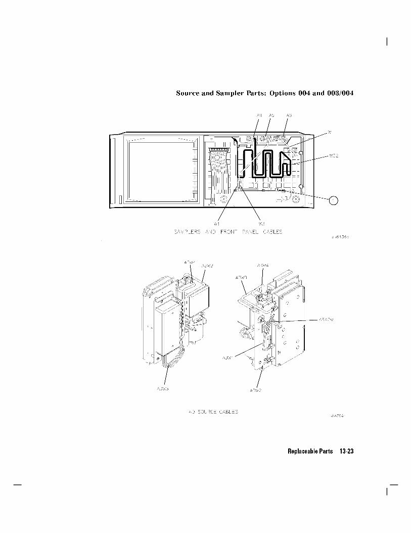
Source and Sampler Parts: Options 004 and 003/004
Replaceable Parts 13-23

Source and Sampler Parts: Option 006
Item HP Part
Number
Qty Description
A3 08753-60233 1 SOURCE ASSY
A3 08753-69233 SOURCE ASSY (Rebuilt-Exchange)
A3MP1 1250-0590 1 SMB CAP
A3W1 08753-20107 1 RF CA, SEMI-RIGID, EYO (A3A3) to SOURCE (A3)
A3W2 08753-20032 1 RF CA, SEMI-RIGID, CAV OSC (A3A4) to SOURCE (A3)
A3A2W1 08753-60034 1 RIBBON CA ASSY, EYO (A3A3) to ALC (A3A2)
A3W7 08752-20024 1 RF CA, 4 dB ATTENUATOR (A3AT1) to BULKHEAD (A3 OUTPUT)
A4 08753-60004 1 R SAMPLER ASSY
A5 08753-60004 1 A SAMPLER ASSY
A6 08753-60169 1 B SAMPLER ASSY
W1 08752-20021 1 RF CA, SOURCE (A3) to COUPLER (A30)
W2 5021-8770 1 RF CA, COUPLER (A30) to R SAMPLER (A4)
W3 5021-8771 1 RF CA, COUPLER (A30) to A SAMPLER (A5)
W34 08752-20023 1 RF CA, TRANSMISSION PORT to 8 dB ATTENUATOR (AT1)
13-24 Replaceable Parts
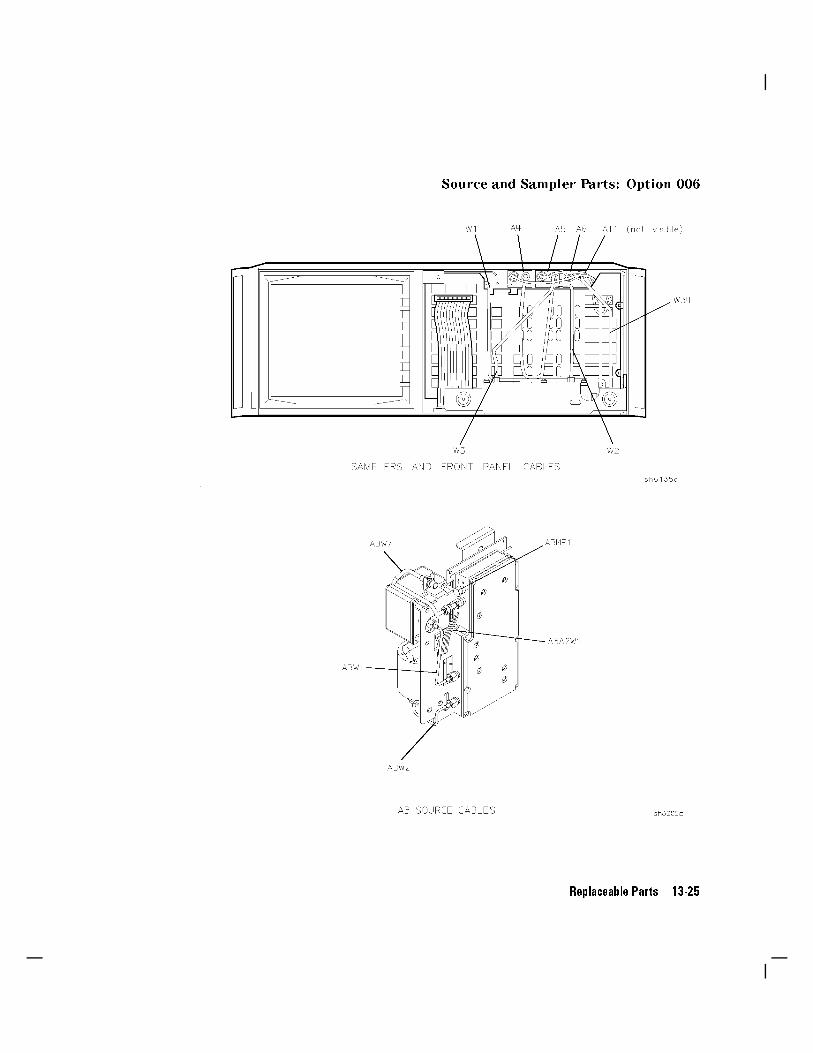
Source and Sampler Parts: Option 006
Replaceable Parts 13-25

Display Bezel Assembly
Item Opt. HP Part
Number
Qty Description
1 08757-40012 1 SOFTKEYS COVER
2 5062-7208 1 BEZEL ASSY (nameplate must be ordered separately)
3* 0515-2113 2 SCREW-MACHINE M4.0�8 PC-PN-TX
4 08752-80032 1 NAMEPLATE 8752C
4 003 08752-80034 1 NAMEPLATE 8752C OPTION 003
4 006 08752-80035 1 NAMEPLATE 8752C OPTION 006
5 08757-40003 1 BEZEL SUPPORT
*Metric hardware: other thread types will damage threaded holes.
13-26 Replaceable Parts

Display Bezel Assembly
Replaceable Parts 13-27

Chassis Parts
Item HP Part
Number
Qty Description
1 5062-3735 1 COVER, TOP ASSY
2 5021-5806 1 REAR FRAME
3 5062-3842 1 COVER-SIDE (for use with strap handle)
4 5062-3704 1 STRAP HANDLE 18 INCH
5 5041-8820 1 STRAP, HANDLE, CAP-REAR
6* 0515-1384 2 SCREW-MACHINE M5.0�10 PC-FL-TX
7 5001-0540 2 TRIM, SIDE (used when front handles are removed)
8 5041-8819 1 STRAP, HANDLE, CAP-FRONT
9 1460-1345 2 TILT STAND
10 5041-8801 4 FOOT (STANDARD)
11 5062-3747 1 COVER, BOTTOM ASSY (order item 11A also)
11A 08753-20039 1 BOTTOM COVER MYLAR INSULATOR (not shown)
12 5062-3817 1 COVER-SIDE-PERF
13 5041-8802 1 TRIM, TOP
14 5062-3990 1 FRONT HANDLE KIT (for rack mount options)
15 5041-8821 4 REAR STANDOFF
16* 0515-1402 4 SCREW-MACHINE M3.5�8 PC-PN-TX
17 5021-8405 1 FRONT FRAME
*Metric hardware: other thread types will damage threaded holes.
NOTE: See \Miscellaneous Parts and Accessories" for touch-up paint.
13-28 Replaceable Parts
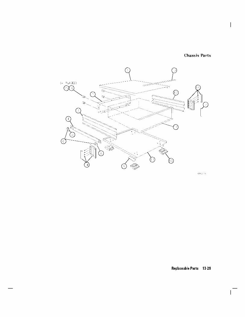
Chassis Parts
Replaceable Parts 13-29

Top View of Attaching Hardware and Post Regulator Fuses
Ref. Desig. HP Part
Number
Qty Description
1* 0515-2086 1 SCREW-MACHINE M4.0�7 PC-FL-TX
2* 0515-1400 2 SCREW-MACHINE M3.5�8 PC-FL-TX
3* 0515-0374 15 SCREW-MACHINE M3.0�10 CW-PN-TX
4* 0515-2035 1 SCREW-MACHINE M3.0�16 PC-FL-TX
5* 0515-0458 2 SCREW-MACHINE M3.5�8 CW-PN-TX
6* 0515-0377 2 SCREW-MACHINE M3.5�10 CW-PN-TX
7* 0515-0390 3 SCREW-MACHINE M4.0�6 CW-FL-TX
8* 0515-0433 1 SCREW-MACHINE M4.0�8 CW-FL-TX
9* 0515-0664 1 SCREW-MACHINE M3.0�12 CW-PN-TX
10 3050-0891 1 WASHER-FLAT M3.0 NOM
A8F1 2110-0425 1 FUSE 2A 125V NTD 0.25�0.27
A8F2 2110-0424 1 FUSE 0.75A 125V NTD 0.25�0.27
A8F3 2110-0425 1 FUSE 2A 125V NTD 0.25�0.27
A8F4 2110-0424 1 FUSE 0.75A 125V NTD 0.25�0.27
A8F5 2110-0476 1 FUSE 4A 125V NTD 0.25�0.27
A8F6 2110-0425 1 FUSE 2A 125V NTD 0.25�0.27
A8F7 2110-0476 1 FUSE 4A 125V NTD 0.25�0.27
A8F8 2110-0047 1 FUSE 1A 125V NTD 0.25�0.27
A8F9 2110-0046 1 FUSE 0.5A 125V NTD 0.25�0.27
MP1 08753-00039 1 A5 ISOLATION GROUNDING CLIP
MP2 08753-00040 1 A7 ISOLATION GROUNDING SHIELD
MP3 08753-40006 1 PC BOARD STABILIZER-BAR
08753-20062 1 PC BOARD STABILIZER-CAP
* 0515-0374 2 SCREW-MACHINE M3.0�10 CW-PN-TX (attaches cap to bar)
MP4 08753-00044 1 SOURCE RETAINER BRACKET
*Metric hardware: other thread types will damage threaded holes.
13-30 Replaceable Parts

Top View of Attaching Hardware and Post Regulator Fuses
Replaceable Parts 13-31

Bottom View of Attaching Hardware
Item HP Part
Number
Qty Description
1* 0515-1400 5 SCREW-MACHINE M3.5�8 PC-FL-TX
2 5180-8500 1 INSULATOR
3* 0515-0377 2 SCREW-MACHINE M3.5�10 CW-PN-TX
4* 0515-0458 2 SCREW-MACHINE M3.5�8 CW-PN-TX
A17 MOTHERBOARD ASSY (see \Major Assemblies")
*Metric hardware: other thread types will damage threaded holes.
13-32 Replaceable Parts

Bottom View of Attaching Hardware
Replaceable Parts 13-33

Right View of Attaching Hardware
Item HP Part
Number
Qty Description
1* 0515-2086 8 SCREW-MACHINE M4.0�7 PC-FL-TX
2* 0515-1400 1 SCREW-MACHINE M3.5�8 PC-FL-TX
*Metric hardware: other thread types will damage threaded holes.
13-34 Replaceable Parts

Left View of Attaching Hardware
Item HP Part
Number
Qty Description
1* 0515-2086 8 SCREW-MACHINE M4.0�7 PC-FL-TX
2* 0515-2086 3 SCREW-MACHINE M4.0�7 PC-FL-TX
3 1460-1573 1 SPRING-EXTENSION .138 OD
4* 0515-0430 1 SCREW-MACHINE M3.0�6 CW-PN-TX
5 08753-00036 1 INSULATOR-SWITCH
6 08753-00048 1 ACTUATOR-LINE SWITCH
7 08757-40005 1 LINE BUTTON
*Metric hardware: other thread types will damage threaded holes.
Replaceable Parts 13-35

Rear Panel Attaching Hardware
Item HP Part
Number
Qty Description
1 2190-0102 4 WASHER-LOCK INTERNAL TEETH 15/32 INCH 0.472-INCH-ID
2 2950-0035 7 NUT-HEX-DOUBLE CHAMFER 15/32-32-THREAD
3 2190-0586 2 WASHER-LOCK HELICAL 4.0 MM 4.1-MM-ID
4 0380-0643 2 STANDOFF-HEX 0.255-INCH-LONG 6-32 THREAD
5 1251-2942 2 LOCK-SUBMIN D CONN (includes lockwashers)
6* 0515-0372 3 SCREW-MACHINE M3.0�8 CW-PN-TX
7 2110-0780 1 FUSE 3A 250V NON-TIME DELAY
*Metric hardware: other thread types will damage threaded holes.
13-36 Replaceable Parts

Replaceable Labels
Item HP Part
Number
Qty Description
1 08752-80003 1 LABEL, LOCATION DIAGRAM
2 7120-4295 1 LABEL, HAZARDOUS VOLTAGE WARNING
3 7120-6999 1 LABEL, LINE VOLTAGE SELECTOR SWITCH
4 7121-2527 1 LABEL, METRIC HARDWARE CAUTION
5 08753-80066 1 LABEL, WARNING CAUTION
6 7121-5125 1 TAG, WARNING ESD SENSITIVE
Replaceable Parts 13-37

Miscellaneous Parts and Accessories
HP Part Number Description
ACCESSORIES
5062-4072 OPT 1CP, RACK MOUNT KIT FOR INSTRUMENTS EQUIPPED WITH HANDLES
0515-1106 REPLACEMENT SCREWS FOR OPT 913
5062-3978 OPT ICM, RACK MOUNT KIT FOR INSTRUMENTS WITHOUT HANDLES
0515-1114 REPLACEMENT SCREWS, OPT 908
HP 85032B 50 OHM-TYPE N CALIBRATION KIT (OPT 001)
HP 85033C 50 OHM-3.5 MM CALIBRATION KIT (OPT 001)
HP 11852B 50-75 MINIMUM LOSS ATTENUATOR
HP 11853A 50 TYPE-N ADAPTER KIT
HP 11878A 50 3.5 MM ADAPTER KIT
HP 11854A 50 BNC ADAPTER KIT
HP 11855A 75 TYPE-N ADAPTER KIT
HP 11856A 75 BNC ADAPTER KIT
8120-4781 50 TYPE-N TEST PORT RETURN CA
8120-2408 75 TYPE-N TEST PORT RETURN CA
9300-0969 ESD WRIST STRAP (SMALL)
9300-1117 ESD WRIST STRAP (MEDIUM)
9300-0970 ESD WRIST STRAP (LARGE)
HP 92175T ESD TABLE MAT
HP 10833A HP-IB CA (1 M, 3.3 FEET)
HP 10833B HP-IB CA (2 M, 6.6 FEET)
HP 10833C HP-IB CA (4 M, 13.2 FEET)
HP 10833D HP-IB CA (0.5 M, 1.7 FEET)
HP 92192A FLOPPY DISKS (box of 10 double-sided 3.5 inch disks)
HP 85043B SYSTEM RACK MOUNT
13-38 Replaceable Parts

Miscellaneous Parts and Accessories
HP Part Number Description
SOFTWARE
08753-10004 HP 8752C EXAMPLE MEASUREMENT PROGRAM DISK
08753-10005 HP 8752C EXAMPLE MEASUREMENT PROGRAM DISK
SERVICE TOOLS
08753-60023 HP 8752C TOOL KIT
DOCUMENTATION
08752-90134 HP 8752C MANUAL SET includes the following:
08752-90135 HP 8752C USER'S GUIDE (includes Quick Reference, 08752-90138)
08752-90137 HP 8752C PROGRAMMING GUIDE
08752-90139 HP 8752C INSTALLATION & QUICK START GUIDE
08752-90157 HP 8752C SYSTEM VERIFICATION AND PERFORMANCE TESTS
08752-90136 HP 8752C SERVICE GUIDE (this manual)
08752-90158 HP 8752C COMPONENT-LEVEL INFORMATION
UPGRADE KITS
HP 11884D 6 GHz UPGRADE KIT (conversion to Opt 006)
HP 11885A 3 GHz RECEIVER UPGRADE KIT (conversion to Opt 003)
HP 85019C TIME DOMAIN UPGRADE KIT (conversion to Opt 010)
08752-60019 ATTENUATOR UPGRADE KIT (conversion to Opt 004)
SERVICE NOTES*
8753A-1 9 EEPROM BACKUP
8753A-5 IMPROVING RELIABILITY OF THE A3 SOURCE ASSEMBLY
TOUCH-UP PAINT
6010-1146 DOVE GRAY PAINT (front panel frame, portions of front handles)
6010-1147 FRENCH GRAY (side, top, bottom covers)
6010-1148 PARCHMENT WHITE (rack mount anges, rack support shelves, front panel)
*To obtain a service note, contact your local HP Service Center.
Replaceable Parts 13-39

Abbreviations
Reference Designations, Abbreviations, and Options
REFERENCE DESIGNATIONS
A . . . . . . . . . . . . . . . . . . . . . . . . . . . . . . . . . . . . . . . . .assembly
B . . . . . . . . . . . . . . . . . . . . . . . . . . . . . . . . . . . . . . . fan; motor
J . . . . . . . electrical connector (stationary portion); jack
RPG . . . . . . . . . . . . . . . . . . . . . . . . . . rotary pulse generator
W . . . . . . . . . . . . . . . . . . . . .cable; transmission path; wire
ABBREVIATIONS
A . . . . . . . . . . . . . . . . . . . . . . . . . . . . . . . . . . . . . . . . . . ampere
ALC . . . . . . . . . . . . . . . . . . . . . . . . . automatic level control
ASSY . . . . . . . . . . . . . . . . . . . . . . . . . . . . . . . . . . . . . .assembly
AUX . . . . . . . . . . . . . . . . . . . . . . . . . . . . . . . . . . . . . . auxiliary
BD . . . . . . . . . . . . . . . . . . . . . . . . . . . . . . . . . . . . . . . . . . . board
CA . . . . . . . . . . . . . . . . . . . . . . . . . . . . . . . . . . . . . . . . . . . cable
COAX . . . . . . . . . . . . . . . . . . . . . . . . . . . . . . . . . . . . . . coaxial
CPU . . . . . . . . . . . . . . . . . . . . . . . . . central processing unit
CW . . . . . . . . . . . . . . . . . . . . . . . . . . conical washer (screws)
D . . . . . . . . . . . . . . . . . . . . . . . . . . . . . . . . . . . . . . . . .diameter
ESD . . . . . . . . . . . . . . . . . . . . . . . . . . electrostatic discharge
EXT . . . . . . . . . . . . . . . . . . . . . . . . . . . . . . . . . . . . . . . external
EYO . . . . . . . . . . . . . . . . . . . . . . . . . . . . . . . . . . YIG oscillator
FL . . . . . . . . . . . . . . . . . . . . . . . . . . . . . . . . athead (screws)
FLX . . . . . . . . . . . . . . . . . . . . . . . . . . . . . . . . . . . . . . . . exible
FP . . . . . . . . . . . . . . . . . . . . . . . . . . . . . . . . . . . . . front panel
FRAC-N . . . . . . . . . . . . . . . . . . . . . . . . . . . . . . . . fractional N
FREQ . . . . . . . . . . . . . . . . . . . . . . . . . . . . . . . . . . . frequency
GHz . . . . . . . . . . . . . . . . . . . . . . . . . . . . . . . . . . . . . . gigahertz
HEX . . . . . . . . . . . . . . . . . . . . . . . . . . . . . . . . . . . . hexagonal
HP . . . . . . . . . . . . . . . . . . . . . . . . . . . . . . . . Hewlett-Packard
HP-IB . . . . . . . . . . . . . . . . Hewlett-Packard interface bus
HX . . . . . . . . . . . . . . . . . . . . . . . . . . . . . . hex recess (screws)
ID . . . . . . . . . . . . . . . . . . . . . . . . . . . . . . . . . . inside diameter
IF . . . . . . . . . . . . . . . . . . . . . . . . . . . intermediate frequency
I/O . . . . . . . . . . . . . . . . . . . . . . . . . . . . . . . . . . . . input/output
LED . . . . . . . . . . . . . . . . . . . . . . . . . . . . light-emitting diode
M . . . . . . . . . . . . . . . . . . . . . . . . . . . . . . . . . . . . . . . . . . .meters
M . . . . . . . . . . . . . . . . . . . . . . . . . . . . . . . . . metric hardware
MHz . . . . . . . . . . . . . . . . . . . . . . . . . . . . . . . . . . . . . megahertz
mm . . . . . . . . . . . . . . . . . . . . . . . . . . . . . . . . . . . . .millimeters
MNL . . . . . . . . . . . . . . . . . . . . . . . . . . . . . . . . . . . . . . . manual
MON . . . . . . . . . . . . . . . . . . . . . . . . . . . . . . . . . . . . . . .monitor
NOM . . . . . . . . . . . . . . . . . . . . . . . . . . . . . . . . . . . . . . nominal
NTD . . . . . . . . . . . . . . . . . . . . . . . . . . . . . . . . . non-time delay
NY . . . . . . . . . . . . . . . . . . . . . . . . . . . . . . . . . . . . . . . . . . . nylon
OD . . . . . . . . . . . . . . . . . . . . . . . . . . . . . . . . outside diameter
Opt . . . . . . . . . . . . . . . . . . . . . . . . . . . . . . . . . . . . . . . . . option
OSC . . . . . . . . . . . . . . . . . . . . . . . . . . . . . . . . . . . . . . oscillator
PC . . . . . . . . . . . . . . . . . . . . . . . . . . . . . . patch lock (screws)
PC . . . . . . . . . . . . . . . . . . . . . . . . . . . . . . . . . . printed circuit
PN . . . . . . . . . . . . . . . . . . . . . . . . . . . . . . . .panhead (screws)
p/o . . . . . . . . . . . . . . . . . . . . . . . . . . . . . . . . . . . . . . . . . .part of
REF . . . . . . . . . . . . . . . . . . . . . . . . . . . . . . . . . . . . . . reference
REPL . . . . . . . . . . . . . . . . . . . . . . . . . . . . . . . . . . replacement
RF . . . . . . . . . . . . . . . . . . . . . . . . . . . . . . . . . radio frequency
RP . . . . . . . . . . . . . . . . . . . . . . . . . . . . . . . . . . . . . . rear panel
SH . . . . . . . . . . . . . . . . . . . . . . . . .socket head cap (screws)
TX . . . . . . . . . . . . . . . . . . . . . . . . . . . . TORX recess (screws)
Qty . . . . . . . . . . . . . . . . . . . . . . . . . . . . . . . . . . . . . . . . quantity
V . . . . . . . . . . . . . . . . . . . . . . . . . . . . . . . . . . . . . . . . . . . . . volt
WFR . . . . . . . . . . . . . . . . . . . . . . . . . . . . . . . . . . wire formed
W/O . . . . . . . . . . . . . . . . . . . . . . . . . . . . . . . . . . . . . . . .without
YIG . . . . . . . . . . . . . . . . . . . . . . . . . . . . . yttrium-iron garnet
OPTIONS
003 . . . . . . . . . . . . . . . . . . . . . . . . . . . . . . 3 GHz performance
004 . . . . . . . . . . . . . . . . . . . . . . . . . . . 70 dB step attenuator
006 . . . . . . . . . . . . . . . . . . . . . . . . . . . . . . 6 GHz performance
010 . . . . . . . . . . . . . . . . . . . . . . . . . . . . . . . . . . . . time domain
075 . . . . . . . . . . . . . . . . . . . . . . . . . . . . . . . . . .75 ohm test set
13-40 Replaceable Parts

14Assembly Replacement and Post-RepairProcedures
This chapter contains procedures for removing and replacing the majorassemblies of the HP 8752C network analyzer. A table showing thecorresponding post-repair procedures for each replaced assembly is located atthe end of this chapter.
Procedures described in this chapter consist of the following:
Cover Removal
Initial Front Panel Procedure
Initial Rear Panel Procedure
A1, A2 (keyboard, front panel interface)
A3 (source)
A15, A16 (preregulator, rear panel board)
A18 (display)
A30 (directional coupler)
B1 (fan)
A9BT1 (battery)
Caution Many of the assemblies in this instrument are very susceptibleto damage from ESD (electrostatic discharge). Perform thefollowing procedures only at a static-safe workstation and weara grounding strap.
Assembly Replacement and Post-Repair Procedures 14-1

Assembly Replacement Sequence
The following steps show the sequence to replace an assembly in an HP 8752CNetwork Analyzer.
1. Identify the faulty group. Refer to the \Start Troubleshooting Here" chapter.Follow up with the appropriate troubleshooting chapter that identi�es thefaulty assembly.
2. Order a replacement assembly. Refer to the \Replaceable Parts" chapter.
3. Replace the faulty assembly and determine what adjustments are necessary.Refer to the \Assembly Replacement and Post-Repair Procedures" chapter.
4. Perform the necessary adjustments. Refer to the \Adjustments and
Correction Constants" chapter.
5. Perform the necessary performance tests. Refer to the \System Veri�cationand Performance Tests" chapter.
Tools Required
ESD wrist strap and grounding cordSmall at edge screwdriverTORX driverNumber 10Number 15Number 25
Wrenches, open end:3/16-inch9/32-inch5/16-inch9/16-inch
14-2 Assembly Replacement and Post-Repair Procedures

Cover Removal Procedure
Figure 14-1. Cover Removal Procedure
To remove top cover: To remove right side cover:
remove screws (1) & upper stando�s (2) remove top cover
loosen screw (3) remove screw (9) & lower stando� (10)
slide cover o� loosen screw (11)
slide cover back
To remove left side cover: To remove bottom cover:
remove top cover remove bottom feet (12)
remove screw (4) & lower stando� (5) remove screws (4,9) & lower stando�s (5,10)
remove screws (6) & handle (7) loosen screw (13)
loosen screw (8) slide cover o�
slide cover back
Assembly Replacement and Post-Repair Procedures 14-3

Initial Front Panel Procedure
Figure 14-2. Initial Front Panel Procedure
1. Remove the bezel's softkey cover (item 1, Figure 14-2) by sliding your�ngernail under the left edge, near the top or bottom of the cover.
2. Pry the cover away from the bezel. Do not scratch the glass.
3. Remove the two screws (item 2) exposed by the previous step.4. Remove the bezel (item 3) from the frame.
5. Remove the trim strip from the top edge of the front frame by prying it witha at screwdriver.
6. Remove the two right-most screws from the top edge of the frame (item 4).
14-4 Assembly Replacement and Post-Repair Procedures

Figure 14-3. Location of Screws on Bottom Edge of Frame
7. Turn the instrument over and remove the right front foot.8. Remove the two screws from the bottom edge of the frame (item 5).9. Continue with the procedure which referred you to this one.
Assembly Replacement and Post-Repair Procedures 14-5

Initial Rear Panel Procedure
1. Remove the top and bottom covers (see \Cover Removal Procedure").2. Remove the PC board stabilizer (item 6, Figure 14-4).
Figure 14-4. Location of EXT REF cable and GSP Assembly
14-6 Assembly Replacement and Post-Repair Procedures

3. Lift the A12 reference assembly from its motherboard connector anddisconnect the EXT REF coax cable (item 7) from A12J3.
4. Remove the A19 GSP assembly clamp (item 8).5. Disconnect the RED, GREEN, and BLUE coax cables from the GSP board (you
may need to move the large ribbon cable to access them).
Figure 14-5. Location of Rear Panel Fasteners
6. Remove seven screws from the rear panel assembly: two from the top andbottom frames (item 9), and three from the back (item 10, Figure 14-5).
7. Pull the rear panel away from the frame. Disconnect the ribbon cable fromits motherboard connector by pressing down and out on the connector locks.
8. Continue with the procedure which referred you to this one.
Assembly Replacement and Post-Repair Procedures 14-7
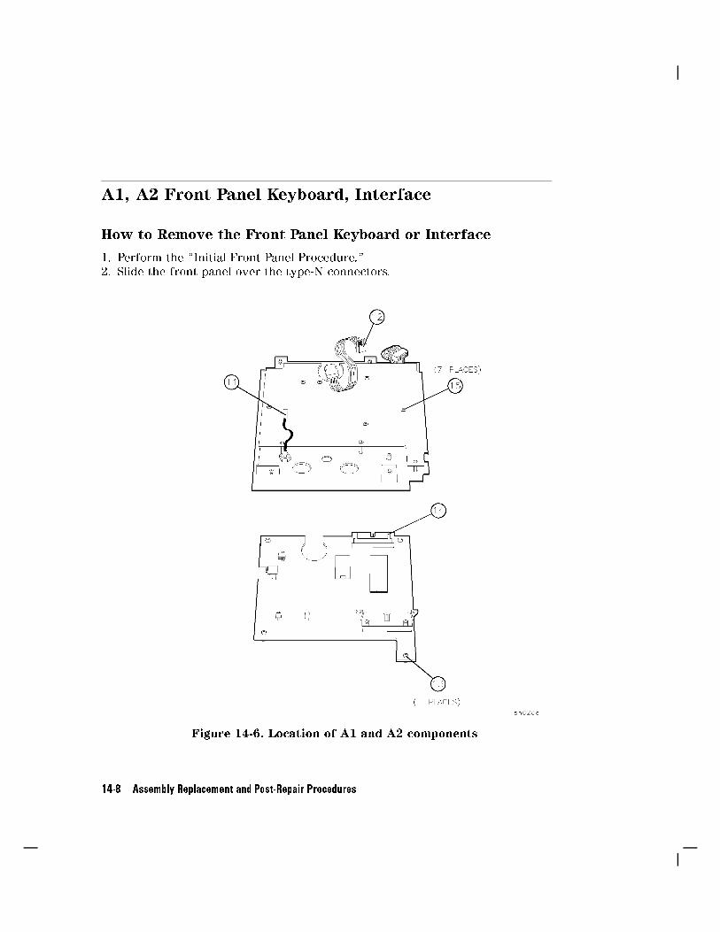
A1, A2 Front Panel Keyboard, Interface
How to Remove the Front Panel Keyboard or Interface
1. Perform the \Initial Front Panel Procedure."2. Slide the front panel over the type-N connectors.
Figure 14-6. Location of A1 and A2 components
14-8 Assembly Replacement and Post-Repair Procedures
3. Disconnect the ribbon cable from the front panel by pressing down and outon the connector locks.
4. Remove the probe power cable (item 11) and the RPG cable (item 12).5. Remove the four screws in the corners of the A2 assembly (item 13).6. Insert the blade of a small at screwdriver into the slots on the sides of the
ribbon cable connector (item 14). Gently pry upwards on either side of theconnector until it is loose.
7. Remove the remaining seven screws from the A1 assembly (item 15).
Reverse Removal Procedure to Reinstall
After reinstallation, refer to \Post-Repair Procedures" at the end of this chapterto ensure that the analyzer operates properly.
Assembly Replacement and Post-Repair Procedures 14-9

A3 Source
How to Remove the Source
1. Remove the power cord and the top cover (see \Cover Removal Procedure").2. Remove the two screws with washers (item 17, Figure 14-7) from the source
retainer bracket. Remove the bracket.
Figure 14-7. Location of Source Parts
3. Disconnect the semi-rigid cables (item 18) at the bulkhead connector andsource.
4. Pull the two retention clips (item 19) at the front and rear of the sourcemodule to an upright position.
5. Push the disconnected cables toward the right side of the analyzer.6. Pull up on the source bracket handle (item 20) and remove the source.
14-10 Assembly Replacement and Post-Repair Procedures

Reverse Removal Procedure to Reinstall
Keep the semi-rigid cables out of the way as you reinstall the source.Make sure the edges of the sheet metal partition slide into the guides at thefront and back of the source compartment.Make sure the source is well seated in the motherboard connector.Remember to push down the retention clips.After reinstallation, refer to \Post-Repair Procedures" at the end of thischapter to ensure that the analyzer operates properly.
Assembly Replacement and Post-Repair Procedures 14-11

A15 Preregulator
How to Remove the Preregulator
1. Perform the \Initial Rear Panel Procedure."
Figure 14-8. Location of Preregulator Fasteners and Wires
14-12 Assembly Replacement and Post-Repair Procedures
2. Remove the remaining four screws (item 22, Figure 14-8) in the rear frame:two on the top and two on the bottom.
3. Disconnect the A15 wire bundle (item 23) from the A8 post-regulator boardassembly.
4. Disconnect the A15 wires (item 24) from the motherboard.5. Pull the preregulator assembly free from the frame.
Reverse Removal Procedure to Reinstall
After reinstallation, refer to \Post-Repair Procedures" at the end of this chapterto ensure that the analyzer operates properly.
Assembly Replacement and Post-Repair Procedures 14-13

A16 Rear Panel Board Assembly
How to Remove the Rear Panel
1. Perform the \Initial Rear Panel Procedure."
Figure 14-9. Location of Rear Panel Fasteners
2. Remove the hex screws (item 26, Figure 14-9) from the HP-IB connector andthe test set interconnect connector.
3. Remove the hex nuts and lock washers (item 27) from the AUX INPUT, EXT
AM, and EXT TRIGGER BNC connectors.4. Remove the rear panel board assembly.
14-14 Assembly Replacement and Post-Repair Procedures

Reverse Removal Procedure to Reinstall
Note Torque the hex screws to 4 in-lb maximum.
After reinstallation, refer to \Post-Repair Procedures" at the end of this chapterto ensure that the analyzer operates properly.
Assembly Replacement and Post-Repair Procedures 14-15

A18 Display
How to Remove the Display
1. Remove the power cord and the top cover (see \Cover Removal Procedure").
Figure 14-10. Location of Display Fasteners and Parts
14-16 Assembly Replacement and Post-Repair Procedures
2. Remove the bezel's softkey cover (item 29, Figure 14-10) by sliding your�ngernail under the left edge, near the top or bottom of the cover.
3. Pry the softkey cover away from the bezel. Take care to not scratch theglass.
4. Remove the two screws (item 30) exposed by the previous step.5. Remove the bezel (item 31) carefully; it is heavy for its size.6. Remove the gasket from the front of the CRT.7. At the A19 GSP assembly, disconnect the grey ribbon cable (item 32) from
the CRT.8. Remove the four screws on the top of the display shield (item 33).9. Start to slide the display out of the instrument by pushing on the back of the
display assembly. There is a hole at the rear of the display shielding whereyou can reach in to push the display.
How to Reinstall the Display
1. Remove and set aside the bottom shield attached to the replacement display.Install the bottom shield on the old display assembly before it is returned forrepair.
2. Leave the ribbon cable (A18W1) in the fastened position for easy retrievalthrough the rear display shielding.
3. Reverse the �rst six steps.
After reinstallation, refer to \Post-Repair Procedures" at the end of this chapter
to ensure that the analyzer operates properly.
Assembly Replacement and Post-Repair Procedures 14-17

A30 Directional Coupler
How to Remove the Directional Coupler
1. Perform the \Initial Front Panel Procedure."
Figure 14-11. Location of Coupler Screws on Bottom Front Frame
14-18 Assembly Replacement and Post-Repair Procedures

2. Remove the three screws which fasten the coupler to the bottom frontframe (item 35, Figure 14-11).
3. Remove the front panel by sliding it out and over the type-N connectors.4. Disconnect the ribbon cable from the front panel by pressing down and out
on the connector locks.5. Remove the trim strip (item 36, Figure 14-12) on the right side of the front
panel by prying under the strip with a at screwdriver.6. Remove the right side front handle (item 37).
Figure 14-12. Location of Directional Coupler Hardware
7. Remove the screw on the side edge of the frame (item 38).8. Disconnect the semi-rigid cables from the coupler.9. Remove the coupler and bracket from the analyzer.10. Remove the screws (item 39) that fasten the bracket to the coupler.11. Disconnect any remaining cables from the coupler.
Reverse Removal Procedure to Reinstall
After reinstallation, refer to \Post-Repair Procedures" at the end of this chapterto ensure that the analyzer operates properly.
Assembly Replacement and Post-Repair Procedures 14-19

B1 Fan
How to Remove the Fan
1. Perform the \Initial Rear Panel Procedure."
Figure 14-13. Location of Fan Wire Bundle and Screws
2. Disconnect the fan's wire bundle from its motherboard connector (item 40,Figure 14-13).
3. Remove the Torx screws (item 41) from the four corners of the fan.
Reverse Removal Procedure to Reinstall
After reinstallation, refer to \Post-Repair Procedures" at the end of this chapter
to ensure that the analyzer operates properly.
14-20 Assembly Replacement and Post-Repair Procedures

A9BT1 Battery
How to Remove the Battery
1. Remove the A9 CPU board from its card cage slot.2. Unsolder and remove the battery from the A9 CPU board.
Warning Battery A9BT1 contains lithium. Do not incinerate or
puncture this battery. Dispose of the discharged battery ina safe manner.
Replacing the Battery
1. Make sure the new battery is inserted into the A9 board with the correctpolarity.
2. Solder the battery into place.
3. Replace the A9 CPU board.
Assembly Replacement and Post-Repair Procedures 14-21

Post-Repair Procedures
After you repair or replace an assembly, check the following table. It lists anyadditional service procedures that must be performed to ensure the instrumentis working properly.
Table 14-1. Post-Repair Procedures
Replaced or Repaired
Assembly
Adjustments
Correction Constants (CC)
Veri�cation
A1 Front Panel
Keyboard
None Internal Test 0
Internal Test 23
A2 Front Panel
Interface
None Internal Test 0
Internal Test 23
Internal Test 12
A3 Source A9 CC Jumper Position
Source Default CC (test 44)
Source Pretune Default CC (Test 45)
Analog Bus CC (Test 46)
RF Output Power (Test 47)
Source Pretune (Test 48)
Frequency Response CC (Tests 53 and 57)
Cavity Oscillator CC (Test 54)
Source Spur Avoidance Tracking
EEPROM Backup Disk
Re ection Test Port
Output Power Range
and Level Linearity
A4/A5/A6 Samplers A9 CC Jumper Position
Frequency Response CC (Tests 53 and 57)
IF Ampli�er CC (Test 51)
EEPROM Backup Disk
Test Port Crosstalk
A7 Pulse Generator A9 CC Jumper Position
Frequency Response CC (Tests 53 and 57)
EEPROM Backup Disk
Re ection Test Port
Output Power Range
and Level Linearity
A8 Post Regulator A9 CC Jumper Position
Source Spur Avoidance Tracking
Cavity Oscillator CC (Test 54)
EEPROM Backup Disk
Internal Test 0
Check A8 Test Point
Voltages
14-22 Assembly Replacement and Post-Repair Procedures

Table 14-1. Post-Repair Procedures (continued)
Replaced or Repaired
Assembly
Adjustments
Correction Constants (CC)
Veri�cation
A9 CPU A9 CC Jumper Position
Model Number CC (75 only)
Display Intensity CC (Test 49)
Serial Number CC (Test 55)
Option Number CC (Test 56)
Source Default CC (Test 44)
Source Pretune Default CC (Test 45)
Analog Bus CC (Test 46)
RF Output Power CC (Test 47)
Source Pretune CC (Test 48)
Frequency response CC (Tests 53 and 57)
ADC O�set CC (Test 52)
IF Ampli�er CC (Test 51)
Cavity Oscillator CC (Test 54)
EEPROM Backup Disk
Re ection Test Port
Output Power Range
and Level Linearity
Magnitude Dynamic Accuracy
Phase Dynamic Accuracy
A10 Digital IF A9 CC Jumper Position
Analog Bus CC (Test 46)
Frequency Response CC (Tests 53 and 57)
IF Ampli�er CC (Test 51)
EEPROM Backup Disk
Transmission Test Port
Input Noise Floor
Test Port Crosstalk
System Trace Noise
A11 Phase Lock A9 CC Jumper Position
Analog Bus CC (Test 46)
Pretune Default CC (Test 45)
Source Pretune CC (Test 45)
EEPROM Backup Disk
Re ection Test Port
Output Frequency Range
and Accuracy
A12 Reference High/Low Band Transition
Frequency Accuracy
Re ection Test Port
Output Frequency Range
and Accuracy
A13 Frac-N (Analog) Frac-N Spur Avoidance and FM
Sideband
Re ection Test Port
Output Frequency Range
and Accuracy
A14 Frac-N (Digital) Frac-N Frequency Range
Frac-N Spur Avoidance and FM Sideband
Re ection Test Port
Output Frequency Range
and Accuracy
A15 Preregulator None Self Test
A16 Rear Panel Board None Internal Test 13
A17 Motherboard None Self Test
A18 Display Vertical Position and Focus
Display Intensity CC (Test 49)
only if needed
Internal Tests 66 - 80
Assembly Replacement and Post-Repair Procedures 14-23
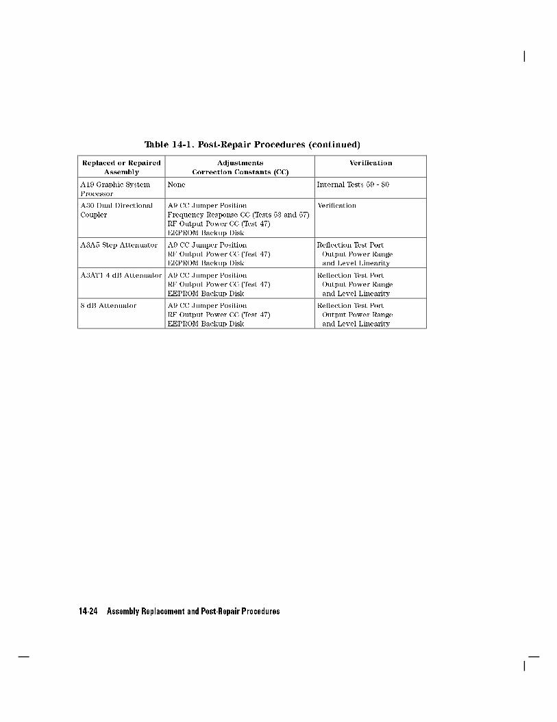
Table 14-1. Post-Repair Procedures (continued)
Replaced or Repaired
Assembly
Adjustments
Correction Constants (CC)
Veri�cation
A19 Graphic System
Processor
None Internal Tests 59 - 80
A30 Dual Directional
Coupler
A9 CC Jumper Position
Frequency Response CC (Tests 53 and 57)
RF Output Power CC (Test 47)
EEPROM Backup Disk
Veri�cation
A3A5 Step Attenuator A9 CC Jumper Position
RF Output Power CC (Test 47)
EEPROM Backup Disk
Re ection Test Port
Output Power Range
and Level Linearity
A3AT1 4 dB Attenuator A9 CC Jumper Position
RF Output Power CC (Test 47)
EEPROM Backup Disk
Re ection Test Port
Output Power Range
and Level Linearity
8 dB Attenuator A9 CC Jumper Position
RF Output Power CC (Test 47)
EEPROM Backup Disk
Re ection Test Port
Output Power Range
and Level Linearity
14-24 Assembly Replacement and Post-Repair Procedures

15
Safety and Licensing
Notice
The information contained in this document is subject to change without notice.
Hewlett-Packard makes no warranty of any kind with regard to this material,
including but not limited to, the implied warranties of merchantability and
�tness for a particular purpose. Hewlett-Packard shall not be liable for errorscontained herein or for incidental or consequential damages in connection withthe furnishing, performance, or use of this material.
Certi�cation
Hewlett-Packard Company certi�es that this product met its published
speci�cations at the time of shipment from the factory. Hewlett-Packard
further certi�es that its calibration measurements are traceable to the UnitedStates National Institute of Standards and Technology, to the extent allowed
by the Institute's calibration facility, and to the calibration facilities of otherInternational Standards Organization members.
Assistance
Product maintenance agreements and other customer assistance agreements areavailable for Hewlett-Packard products.
For any assistance, contact your nearest Hewlett-Packard Sales and Service
O�ce.
Safety and Licensing 15-1
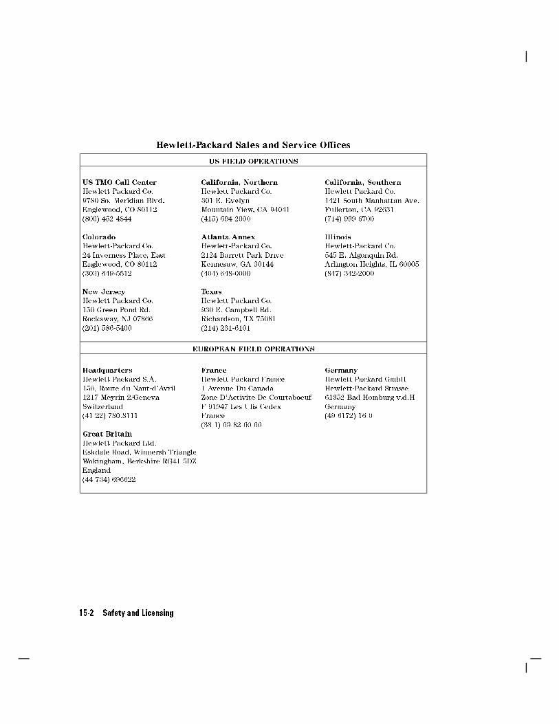
Hewlett-Packard Sales and Service O�ces
US FIELD OPERATIONS
US TMO Call Center California, Northern California, Southern
Hewlett-Packard Co. Hewlett-Packard Co. Hewlett-Packard Co.
9780 So. Meridian Blvd. 301 E. Evelyn 1421 South Manhattan Ave.
Englewood, CO 80112 Mountain View, CA 94041 Fullerton, CA 92631
(800) 452-4844 (415) 694-2000 (714) 999-6700
Colorado Atlanta Annex Illinois
Hewlett-Packard Co. Hewlett-Packard Co. Hewlett-Packard Co.
24 Inverness Place, East 2124 Barrett Park Drive 545 E. Algonquin Rd.
Englewood, CO 80112 Kennesaw, GA 30144 Arlington Heights, IL 60005
(303) 649-5512 (404) 648-0000 (847) 342-2000
New Jersey Texas
Hewlett-Packard Co. Hewlett-Packard Co.
150 Green Pond Rd. 930 E. Campbell Rd.
Rockaway, NJ 07866 Richardson, TX 75081
(201) 586-5400 (214) 231-6101
EUROPEAN FIELD OPERATIONS
Headquarters France Germany
Hewlett-Packard S.A. Hewlett-Packard France Hewlett-Packard GmbH
150, Route du Nant-d'Avril 1 Avenue Du Canada Hewlett-Packard Strasse
1217 Meyrin 2/Geneva Zone D'Activite De Courtaboeuf 61352 Bad Homburg v.d.H
Switzerland F-91947 Les Ulis Cedex Germany
(41 22) 780.8111 France (49 6172) 16-0
(33 1) 69 82 60 60
Great Britain
Hewlett-Packard Ltd.
Eskdale Road, Winnersh Triangle
Wokingham, Berkshire RG41 5DZ
England
(44 734) 696622
15-2 Safety and Licensing
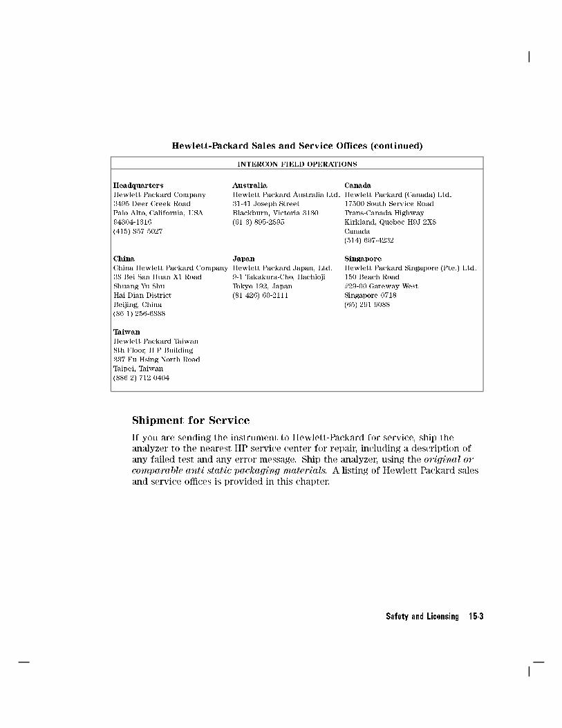
Hewlett-Packard Sales and Service O�ces (continued)
INTERCON FIELD OPERATIONS
Headquarters Australia Canada
Hewlett-Packard Company Hewlett-Packard Australia Ltd. Hewlett-Packard (Canada) Ltd.
3495 Deer Creek Road 31-41 Joseph Street 17500 South Service Road
Palo Alto, California, USA Blackburn, Victoria 3130 Trans-Canada Highway
94304-1316 (61 3) 895-2895 Kirkland, Quebec H9J 2X8
(415) 857-5027 Canada
(514) 697-4232
China Japan Singapore
China Hewlett-Packard Company Hewlett-Packard Japan, Ltd. Hewlett-Packard Singapore (Pte.) Ltd.
38 Bei San Huan X1 Road 9-1 Takakura-Cho, Hachioji 150 Beach Road
Shuang Yu Shu Tokyo 192, Japan #29-00 Gateway West
Hai Dian District (81 426) 60-2111 Singapore 0718
Beijing, China (65) 291-9088
(86 1) 256-6888
Taiwan
Hewlett-Packard Taiwan
8th Floor, H-P Building
337 Fu Hsing North Road
Taipei, Taiwan
(886 2) 712-0404
Shipment for Service
If you are sending the instrument to Hewlett-Packard for service, ship theanalyzer to the nearest HP service center for repair, including a description ofany failed test and any error message. Ship the analyzer, using the original or
comparable anti-static packaging materials. A listing of Hewlett-Packard salesand service o�ces is provided in this chapter.
Safety and Licensing 15-3

Safety Symbols
The following safety symbols are used throughout this manual. Familiarizeyourself with each of the symbols and its meaning before operating thisinstrument.
Caution Caution denotes a hazard. It calls attention to a procedurethat, if not correctly performed or adhered to, would result in
damage to or destruction of the instrument. Do not proceedbeyond a caution note until the indicated conditions are fullyunderstood and met.
Warning Warning denotes a hazard. It calls attention to a procedure
which, if not correctly performed or adhered to, could
result in injury or loss of life. Do not proceed beyond
a warning note until the indicated conditions are fullyunderstood and met.
15-4 Safety and Licensing

Instrument Markings
L The instruction documentation symbol. The product is marked withthis symbol when it is necessary for the user to refer to the instructions in thedocumentation.
\CE" The CE mark is a registered trademark of the European Community. (Ifaccompanied by a year, it is when the design was proven.)
\ISM1-A" This is a symbol of an Industrial Scienti�c and Medical Group 1 ClassA product.
\CSA" The CSA mark is a registered trademark of the Canadian StandardsAssociation.
Safety and Licensing 15-5
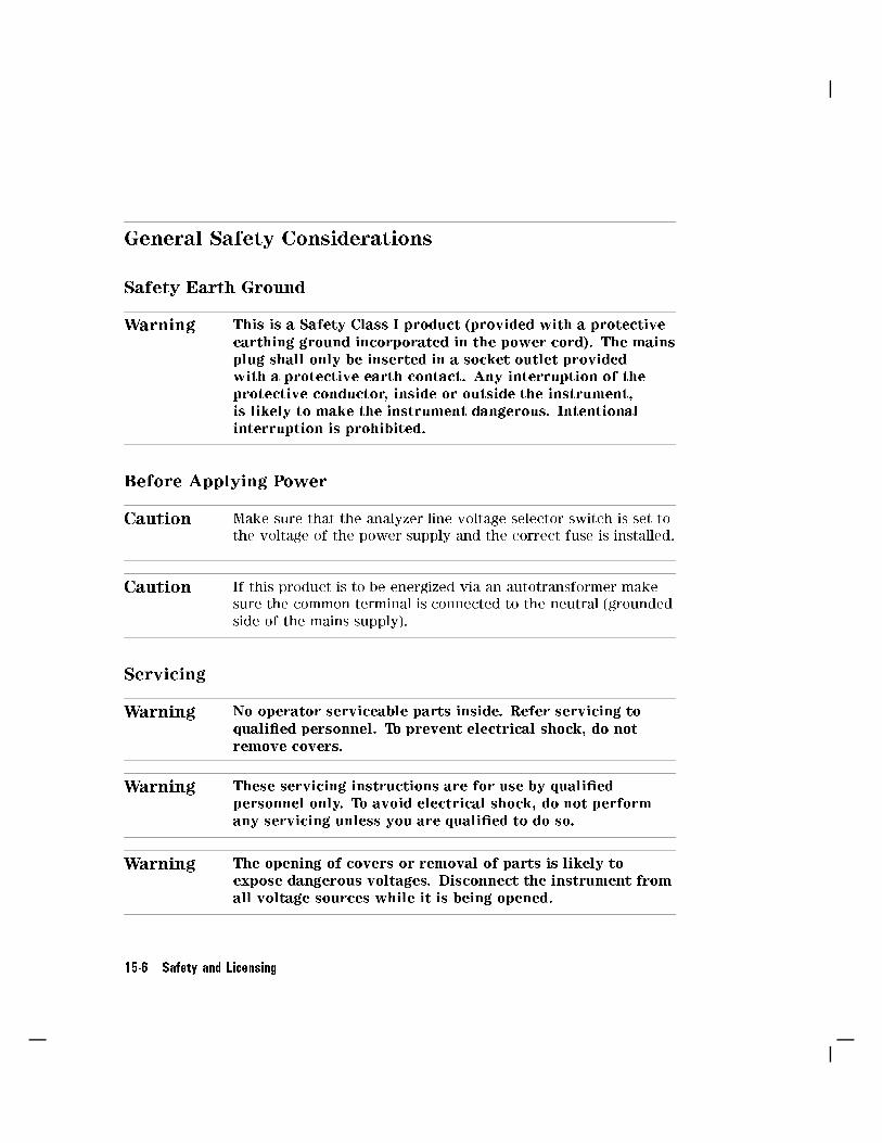
General Safety Considerations
Safety Earth Ground
Warning This is a Safety Class I product (provided with a protective
earthing ground incorporated in the power cord). The mainsplug shall only be inserted in a socket outlet providedwith a protective earth contact. Any interruption of theprotective conductor, inside or outside the instrument,is likely to make the instrument dangerous. Intentionalinterruption is prohibited.
Before Applying Power
Caution Make sure that the analyzer line voltage selector switch is set tothe voltage of the power supply and the correct fuse is installed.
Caution If this product is to be energized via an autotransformer makesure the common terminal is connected to the neutral (groundedside of the mains supply).
Servicing
Warning No operator serviceable parts inside. Refer servicing to
quali�ed personnel. To prevent electrical shock, do notremove covers.
Warning These servicing instructions are for use by quali�edpersonnel only. To avoid electrical shock, do not perform
any servicing unless you are quali�ed to do so.
Warning The opening of covers or removal of parts is likely toexpose dangerous voltages. Disconnect the instrument from
all voltage sources while it is being opened.
15-6 Safety and Licensing
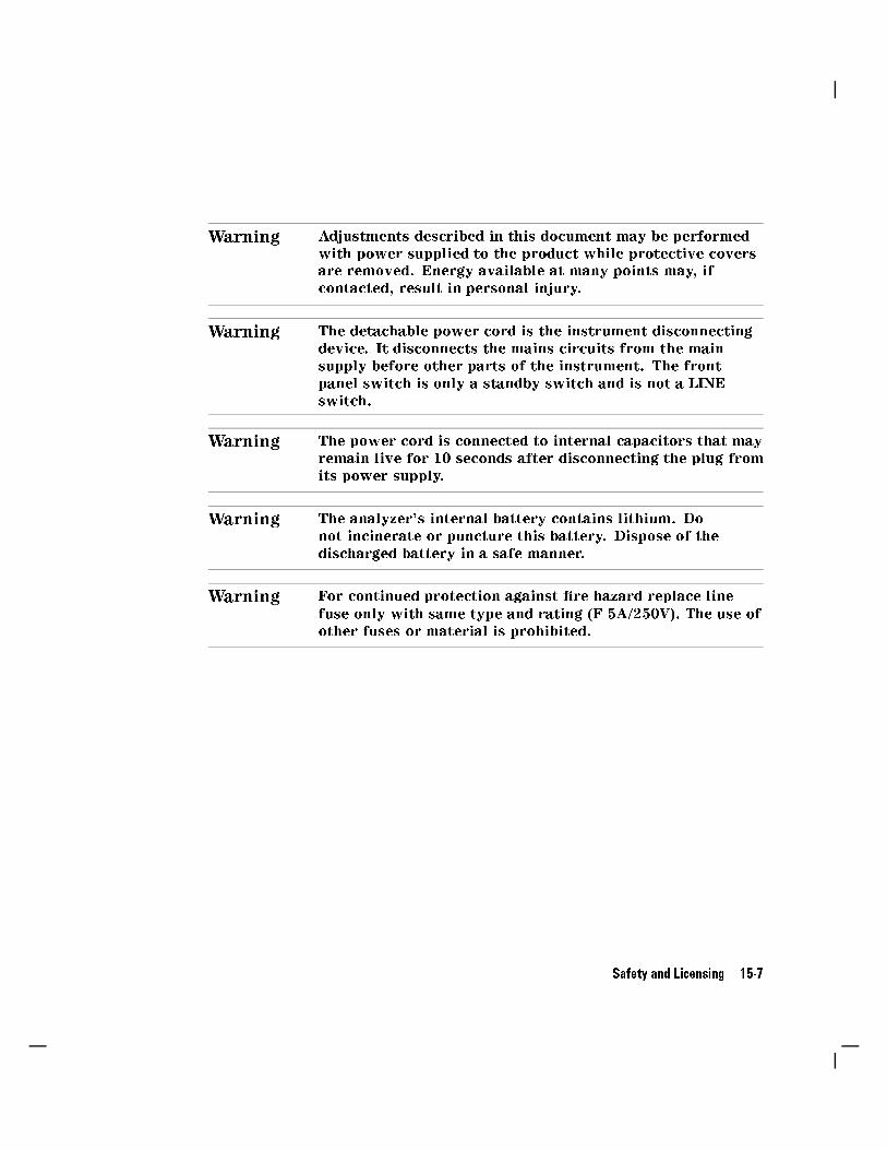
Warning Adjustments described in this document may be performedwith power supplied to the product while protective coversare removed. Energy available at many points may, ifcontacted, result in personal injury.
Warning The detachable power cord is the instrument disconnectingdevice. It disconnects the mains circuits from the mainsupply before other parts of the instrument. The frontpanel switch is only a standby switch and is not a LINEswitch.
Warning The power cord is connected to internal capacitors that may
remain live for 10 seconds after disconnecting the plug from
its power supply.
Warning The analyzer's internal battery contains lithium. Donot incinerate or puncture this battery. Dispose of the
discharged battery in a safe manner.
Warning For continued protection against �re hazard replace line
fuse only with same type and rating (F 5A/250V). The use ofother fuses or material is prohibited.
Safety and Licensing 15-7

Index
1
100 kHz pulses, 7-1610 MHz HI OUT Waveform from
A14J1, 7-271st LO signal at sampler/mixer, 8-12
2
25 MHz HI OUT Waveform from
A14J1, 7-272nd IF (4 kHz) signal locations, 8-122nd LO locations, 8-132ND LO waveforms, 7-21
4
4 kHz signal check, 8-114 MHz reference signal, 7-204 MHz REF signal check, 8-8
5
+5V digital supplytheory of operation, 12-7
6
60 MHz HI OUT Waveform fromA14J1, 7-27
8
8752Ctheory of operation, 12-1
A
A10 assembly signals required, 8-9A10 check by substitution or signal
examination, 8-8A10 digital IF, 12-29digital control, 12-11
A10 Digital IF, 10-36A11 input signals, 7-37A11 Input Signals, 7-38A11 phase lock, 10-37source, 12-15
A11 phase lock and A3 source check,7-8
A11 phase lock check, 7-37A12 digital control signals check,
7-23A12 reference, 10-44source, 12-14
A12 reference check, 7-13A13/A14 Fractional-N Check, 7-24A13 frac-N analogsource, 12-14
A14 Divide-by-N Circuit Check, 7-29A14 frac-N digitalsource, 12-14
A14 fractional-N (digital), 10-47A14 generated digital control signals,
7-31A14-to-A13 digital control signals
check, 7-30A14 VCO exercise, 7-28A15 preregulator
Index-1

removal, 14-12theory of operation, 12-6
A15 preregulator check, 5-9A15W1 plug detail, 5-10A16 rear paneldigital control, 12-13
A16 rear panel boardremoval, 14-14
A18 displaydigital control, 12-12power, 12-9removal, 14-16
A18 display operation check, 6-7A18 power supply voltages, 6-13A19 graphics system processordigital control, 12-12
A19 GSPdigital control, 12-12
A19 GSP and A18 display operationcheck, 6-7
A19 power supply voltages for display,6-13
A19 walking one pattern, 6-16A1/A2 front panel troubleshooting,
6-7A1 front panel keyboard
digital control, 12-10removal, 14-8
A2 front panel interfaceremoval, 14-8
A2 front panel processor
digital control, 12-11A30 directional couplerremoval, 14-18
A30 dual directional coupler, 12-23A3 sourcehigh band theory, 12-19low band theory, 12-16removal, 14-10source, 12-15theory of operation, 12-3, 12-14
A3 source and A11 phase lock check,7-8
A4 R sampler/mixer, 12-28A4 sampler/mixer check, 7-6A5 A sampler/mixer, 12-28A6 B sampler/mixer, 12-28A7 pulse generatorsource, 12-14
A7 pulse generator check, 7-33
A8 fuses and voltages, 5-14
A8 post regulatorair ow detector, 12-8display power, 12-9green LEDs, 12-8probe power, 12-9shutdown circuit, 12-8theory of operation, 12-8variable fan circuit, 12-8
A8 post regulator test points, 5-5A9BT1 batteryremoval, 14-21
A9 CC jumper position adjustment,3-5
A9 CC jumper positions, 10-8A9 CPUdigital control, 12-11
A9 CPU operation check, 6-4ABUS Cor., 10-14
ABUS Test., 10-11accessoriespart numbers, 13-38
accessories inspection, 9-3
accessories troubleshooting chapter,9-1
adapters, 1-3ADC Hist., 10-12ADC Lin., 10-10ADC main, 10-25ADC o�set correction constants (test
#52) adjustment, 3-21ADC Ofs., 10-10
Index-2

ADC Ofs Cor., 10-14ADD, 10-6addresses for HP-IB systems, 4-7adjustmentA9 CC jumper position, 3-5ADC o�set correction constants
(test #52), 3-21analog bus correction constants
(Test #46), 3-10analyzer top cover removal, 3-4cavity oscillator frequency
correction constants (test #54),3-24
display degaussing (demagnetizing),3-45
display intensity adjustments (test
#49), 3-15EEPROM backup disk procedure,
3-38error messages, 3-1fractional-N frequency range, 3-46fractional-N spur avoidance and
FM sideband, 3-54frequency accuracy, 3-49frequency response correction
constants (tests #53 and #57),3-22
high/low band transition, 3-51IF ampli�er correction constants
(test #51), 3-19
initialize EEPROMs (test 58), 3-37model number correction constant
(option 075 only), 3-42option numbers correction constant
(test #56), 3-34order of performance, 3-2RF output power correction
constants (test #47), 3-11serial number correction constant
(test #55), 3-32
source default correction constants(test #44), 3-8
source pretune correction constants(test #48), 3-14
source pretune default correctionconstants (test #45), 3-9
source spur avoidance tracking,3-58
test equipment speci�cations, 3-3
vertical position and focus, 3-43
when to perform, 3-1adjustmentstest equipment speci�cations, 1-1
adjustment tests, 10-3Adjustment Tests, 10-14
ADJUSTMENT TESTS, 10-5
air ow detector, 12-8ALC ON OFF, 10-20ALL INT, 10-7analog bus, 10-25ANALOG BUS, 10-28analog bus check of reference
frequencies, 7-13analog bus checks YO coil drive, 7-11
analog bus codes, 10-53
analog bus correction constants (Test
#46) adjustment, 3-10analog bus node 1, 10-30analog bus node 11, 10-37analog bus node 12, 10-37
analog bus node 13,14, 10-38analog bus node 15, 10-39analog bus node 16, 10-40analog bus node 17, 10-41analog bus node 18, 10-42analog bus node 19, 10-43analog bus node 2, 10-31analog bus node 20, 10-43analog bus node 21, 10-44analog bus node 23, 10-45analog bus node 24, 10-46
Index-3

analog bus node 27, 10-47analog bus node 29, 10-48analog bus node 3, 10-32analog bus node 30, 10-49analog bus node 4, 10-33analog bus node 5, 10-34analog bus node 6, 10-34analog bus node 7, 10-35analog bus node 8, 10-35analog bus node 9, 10-36analog bus nodes, 10-29A3, 10-29
ANALOG BUS ON OFF, 10-24analog in menu, 10-27analog node 10, 10-36analyzer
theory of operations, 12-1analyzer block diagram, 4-16analyzer HP-IB address, 4-7analyzer options available, 1-7analyzer (spectrum), 1-3antistatic wrist strap, 1-3appendix for source group
troubleshooting, 7-39assembliespart numbers, 13-6rebuilt-exchange, 13-2
assembly replacement, 14-1A15 preregulator, 14-12A16 rear panel board, 14-14A18 display, 14-16A1 front panel keyboard, 14-8A2 front panel interface, 14-8A30 directional coupler, 14-18A3 source, 14-10A9BT1 battery, 14-21B1 fan, 14-20covers, 14-3front panel, 14-4rear panel, 14-6tools, 14-2
assembly replacement sequence, 4-2assistance, 15-1attenuatortheory of operation, 12-3
attenuators (�xed), 1-3attenuator (step), 1-3AUX OUT ON OFF, 10-27available options, 1-7
B
B1 fanremoval, 14-20
bad cables, 9-1batteryremoval, 14-21
BATTERY FAILED. STATE MEMORY
CLEARED, 10-54BATTERY LOW! STORE SAVE REGS
TO DISK, 10-54block diagram, 4-16digital control group, 6-3power supply, 5-24power supply functional group,
5-3broadband power problems, 7-40built-in test set, 12-23bulk tape eraser or demagnetizer,
1-3busanalog, 10-25
bus nodes, 10-29
C
cable inspection, 6-10cables, 1-3part numbers, 13-12, 13-14, 13-16,
13-18{25cable test, 9-5CAL FACTOR SENSOR A, 10-6
CAL FACTOR SENSOR B, 10-6
CALIBRATION ABORTED, 10-54
Index-4

calibration coe�cients, 11-1calibration device inspection, 9-3calibration kit 7 mm, 50, 1-3calibration kit device veri�cation,
9-4calibration kit type-N, 75, 1-3calibration procedure, 11-4, 11-6CALIBRATION REQUIRED, 10-55
care of connectors, 1-5
CAUTION: OVERLOAD ON REFL PORT,POWER REDUCED, 8-2
CAUTION: OVERLOAD ON TRANSPORT, POWER REDUCED, 8-2
cavity oscillator frequency correctionconstants (test #54) adjustment,3-24
Cav Osc Cor., 10-14CC proceduresinitialize EEPROMs (test 58), 3-37
center conductor damage, 9-3certi�cation, 15-1characteristicstype-N test port (50), 2-6type-N test port (50) directivity,
2-6type-N test port (50) load match,
2-7type-N test port (50) re ection
tracking, 2-6type-N test port (50) source match
(re ection), 2-6type-N test port (50) source match
(transmission), 2-6type-N test port (50) transmission
tracking, 2-7type-N test port (75), 2-7type-N test port (75) directivity,
2-7type-N test port (75) load match,
2-8
type-N test port (75) re ectiontracking, 2-8
type-N test port (75) source match(re ection), 2-7
type-N test port (75) source match(transmission), 2-8
type-N test port (75) transmissiontracking, 2-8
chassispart numbers, 13-28
check1st LO signal at sampler/mixer,
8-124 MHz REF signal, 8-8A10 by substitution or signal
examination, 8-8
A11 phase lock, 7-37A12 digital control signals, 7-23A12 reference, 7-13A13/A14 Fractional-N, 7-24A14 Divide-by-N Circuit Check,
7-29A14-to-A13 digital control signals,
7-30A15 Preregulator, 5-9A19 GSP and A18 display operation,
6-7A1/A2 front panel, 6-7A3 source and A11 phase lock, 7-8A4 sampler/mixer, 7-6A7 pulse generator, 7-33A8 fuses and voltages, 5-14A9 CPU control, 6-4CPU control, 6-4digital control, 4-12disk drive, 4-8fan voltages, 5-22FN LO at A12, 7-19for a faulty assembly, 5-11GSP and A18 display operation,
6-7
Index-5

HP-IB systems, 4-7line voltage, selector switch, fuse,
5-7motherboard, 5-13operating temperature, 5-13operation of A19 GSP and A18
display, 6-7operation of A9 CPU, 6-4phase lock error message, 7-4plotter or printer, 4-8post regulator voltages, 5-5power supply, 4-11power supply voltages for display,
6-13power up sequence, 4-12preregulator LEDs, 4-11R, A, and B inputs, 8-4rear panel LEDs, 4-11the 4 kHz signal, 8-11YO coil drive with analog bus, 7-11
check front panel cables, 6-10
cleaning of connectors, 1-5CLEAR LIST, 10-6CMOS RAM, 10-7coax cable, 1-3codes for analog bus, 10-53coe�cients, 11-1comb tooth at 3 GHz, 7-34components related to speci�c error
terms, 9-3connection techniques, 1-5connectorcare of, 1-5
CONTINUE TEST, 10-5controller HP-IB address, 4-7controller troubleshooting, 4-9conventions for symbols, 10-52correction constants, 3-1initialize EEPROMs (test 58), 3-37
CORRECTION CONSTANTS NOT
STORED, 10-55
CORRECTION TURNED OFF, 10-55counter, 10-25COUNTEROFF, 10-27
counter (frequency), 1-3counter readout location, 10-41cover removal, 14-3CPU
digital control, 12-11CPU operation check, 6-4CPU walking one pattern, 6-16CRT demagnetizer or bulk tape eraser,
1-3CURRENT PARAMETER NOT IN CAL
SET, 10-55customer assistance, 15-1
D
damage to center conductors, 9-3DEADLOCK, 10-55DELETE, 10-6demagnetizer or bulk tape eraser,
1-3description of tests, 10-7DEVICEnot on, not connect, wrong addrs,
10-56diagnose softkey, 10-7diagnosticerror terms, 11-2
diagnostic LEDs for A15, 5-4diagnostic routines for phase lock,
7-40diagnosticsinternal, 10-2
diagnostics of analyzer, 4-3diagnostic tests, 6-11diagramA4 sampler/mixer to phase lock
cable, 7-7digital control group, 6-3
Index-6
diagram of HP 8752C, 4-16diagram of power supply, 5-24DIF Control, 10-9DIF Counter, 10-9digital controlA10 digital IF, 12-11A16 rear panel, 12-13A18 display, 12-12A19 graphics system processor,
12-12A19 GSP, 12-12A1 front panel keyboard, 12-10A2 front panel processor, 12-11A9 CPU, 12-11digital signal processor, 12-12EEPROM, 12-12main CPU, 12-11main RAM, 12-11theory of operation, 12-9
digital control block diagram, 6-3digital control check, 4-12digital control lines observed using
L INTCOP as trigger, 8-10digital control signals A14-to-A13
check, 7-30digital control signals check, 7-23digital control signals generated from
A14, 7-31digital control troubleshooting
chapter, 6-1digital data lines observed using L
INTCOP as trigger, 8-10digital IF, 10-36, 12-29digital control, 12-11
digital voltmeter, 1-3directional couplerremoval, 14-18
directivity characteristicstype-N test port (50), 2-6type-N test port (75), 2-7
directivity (ED), 11-11
disable shutdown circuitry, 5-16DISKnot on, not connected, wrong addrs,
10-56disk drive check, 4-8disk drive (external) HP-IB address,
4-7disk ( oppy), 1-3DISK HARDWARE PROBLEM, 10-56DISK MESSAGE LENGTH ERROR,
10-56DISK READ/WRITE ERROR, 10-57Disp 2 Ex., 10-14Disp/cpu com., 10-16displaydigital control, 12-12power, 12-9removal, 14-16
display bezelpart numbers, 13-26
display degaussing (demagnetizing),3-45
display intensity adjustments (test#49), 3-15
display operation check, 6-7display power supply on A19, 6-13display tests, 10-3, 10-16DISPLAY TESTS, 10-5
DIV FRAC N, 10-28Divide-by-N Circuit Check, 7-29DONE, 10-6DRAM cell, 10-16DSP ALU, 10-9DSP Control, 10-10DSP Intrpt, 10-9DSP RAM, 10-9DSP Wr/Rd, 10-9dual directional coupler, 12-23
Index-7

E
earth ground wire and static-controltable mat, 1-3
EDIT, 10-6edit list menu, 10-6EEPROM backup disk procedure,
3-38equipmentA9 CC jumper position adjustment,
3-5ADC o�set correction constants
adjustment, 3-21analog bus correction constants
adjustment, 3-10cavity oscillator frequency
correction constants
adjustment, 3-24display degaussing, 3-45display intensity adjustment, 3-15EEPROM backup disk procedure,
3-38fractional-N frequency range
adjustment, 3-46fractional-N spur avoidance and
FM sideband adjustment, 3-54frequency accuracy adjustment,
3-49frequency response correction
constants adjustment, 3-22high/low band transition
adjustment, 3-51IF ampli�er correction constants
adjustment, 3-19model number correction constant
adjustment (option 075 only),3-42
option numbers correction constantadjustment, 3-34
RF output power correctionconstants adjustment, 3-11
serial number correction constantadjustment, 3-32
source default correction constantsadjustment, 3-8
source pretune correction constantsadjustment, 3-14
source pretune default correctionconstants adjustment, 3-9
source spur avoidance trackingadjustment, 3-58
vertical position and focusadjustments, 3-43
equipment for service, 1-1errorBATTERY FAILED. STATE MEMORY
CLEARED, 10-54
BATTERY LOW! STORE SAVE REGSTO DISK, 10-54
CALIBRATION ABORTED, 10-54
CALIBRATION REQUIRED, 10-55
CORRECTION CONSTANTS NOT
STORED, 10-55CORRECTION TURNED OFF, 10-55CURRENT PARAMETER NOT IN
CAL SET, 10-55DEADLOCK, 10-55DEVICE: not on, not connect,
wrong addrs, 10-56DISK HARDWARE PROBLEM,
10-56DISK MESSAGE LENGTH ERROR,
10-56DISK: not on, not connected, wrong
addrs, 10-56DISK READ/WRITE ERROR, 10-57INITIALIZATION FAILED, 10-57
NO CALIBRATION CURRENTLY IN
PROGRESS, 10-57NO IF FOUND: CHECK R INPUT
LEVEL, 10-58
Index-8
NO PHASE LOCK: CHECK R INPUTLEVEL, 10-58
NO SPACE FOR NEW CAL. CLEARREGISTERS, 10-58
NOT ENOUGH SPACE ON DISKFOR STORE, 10-57
OVERLOAD ON INPUT R, POWERREDUCED, 10-59
OVERLOAD ON REFL PORT,POWER REDUCED, 10-58
OVERLOAD ON TRANS PORT,POWER REDUCED, 10-59
PHASE LOCK CAL FAILED, 10-59
PHASE LOCK LOST, 10-60
POSSIBLE FALSE LOCK, 10-60
POWER SUPPLY HOT!, 10-61
POWER SUPPLY SHUT DOWN!,10-61
POWER UNLEVELED, 10-60POW MET INVALID, 10-60
POW MET: not on, not connected,wrong addrs, 10-61
POW MET NOT SETTLED, 10-60PRINTER: not on, not connected,
wrong addrs, 10-61PROBE POWER SHUT DOWN!,
10-62SAVE FAILED. INSUFFICIENT
MEMORY, 10-62SELF TEST #n FAILED, 10-62
SOURCE POWER TRIPPED, RESETUNDER POWER MENU, 10-62
SWEEP MODE CHANGED TO CWTIME SWEEP, 10-63
SYSTEM IS NOT IN REMOTE, 10-63TEST ABORTED, 10-63TROUBLE! CHECK SETUP AND
START OVER, 10-63WRONG DISK FORMAT, INITIALIZE
DISK, 10-63error-correction procedure, 11-4
error message for phase lock, 7-4error messages, 10-1, 10-54during adjustments, 3-1
error messages for receiver failure,8-2
error term inspection, 9-3error terms, 11-1directivity (ED), 11-11
isolation (crosstalk, EX), 11-17re ection tracking (ER), 11-15source match (ES), 11-13transmission tracking (ET), 11-19
E-terms, 11-1external tests, 10-3, 10-12EXTERNAL TESTS, 10-4
F
failureA11 phase lock and A3 source
check, 7-8A19 GSP and A18 display operation,
6-7A1/A2 front panel, 6-7key stuck, 6-8of self test, 4-3phase lock error, 7-4receiver, 8-2RF power from source, 7-3
failuresHP-IB, 6-18
fanair ow detector, 12-8removal, 14-20variable fan circuit, 12-8
fan speeds, 5-22fan troubleshooting, 5-22fan voltages, 5-22faulty analyzer repair, 4-2faulty cables, 9-1faulty calibration devices or
connectors, 9-1
Index-9

faulty group isolation, 4-10�lter (low pass), 1-3�rmware revision softkey, 10-51 oppy disk, 1-3FM Coil { plot with 3 point sweep,
7-38FM sideband and spur avoidance
adjustment, 3-54
FN Count., 10-11
FN LO at A12 check, 7-19
FN LO waveform at A12J1, 7-19FRAC N, 10-28frac-N analogsource, 12-14
Frac N Cont., 10-10frac-N digital
source, 12-14FRACN TUNE mode HI OUT signal,
7-35FRACN TUNE ON OFF, 10-20
Fractional-N Check, 7-24
fractional-N (digital), 10-47fractional-N frequency range
adjustment, 3-46fractional-N spur avoidance and FM
sideband adjustment, 3-54
frequency accuracy adjustment, 3-49frequency counter, 1-3, 10-25frequency output in SRC tune mode,
7-8
frequency response correctionconstants (tests #53 and #57)adjustment, 3-22
front panelpart numbers, 13-8
front panel cables, 13-14front panel hardware, 13-14front panel interfaceremoval, 14-8
front panel keyboarddigital control, 12-10
removal, 14-8front panel key codes, 6-8front panel probe power voltages,
5-19front panel processordigital control, 12-11
front panel removal, 14-4front panel troubleshooting, 6-7Fr Pan Diag., 10-12Fr Pan Wr/Rd, 10-10functional group fault location, 4-10functional groupstheory of operation, 12-5
fuse check, 5-7
G
graphics system processordigital control, 12-12
green LED on A15power supply shutdown, 12-7
green LEDs on A8, 12-8GSPdigital control, 12-12
GSP operation check, 6-7
H
hardkeys, 10-2hardwarepart numbers, 13-14, 13-16, 13-30,
13-32, 13-34, 13-35, 13-36HB FLTR SW ON OFF, 10-21Hewlett-Packard servicing, 4-2high band REF signal, 7-17high/low band transition adjustment,
3-51high quality comb tooth at 3 GHz,
7-34HI OUT signal in FRACN TUNE mode,
7-35H MB line, 7-32how to
Index-10

adjust A9 CC jumper position, 3-5adjust ADC o�set correction
constants, 3-21adjust analog bus correction
constants, 3-10adjust cavity oscillator frequency
correction constants, 3-24adjust display intensity, 3-15adjust fractional-N spur avoidance
and FM sideband, 3-54adjust frequency accuracy, 3-49adjust frequency response
correction constants, 3-22adjust high/low band transition,
3-51adjust IF ampli�er correction
constants, 3-19adjust model number correction
constant (option 075 only),3-42
adjust option numbers correctionconstant, 3-34
adjust RF output power correctionconstants, 3-11
adjust serial number correctionconstant, 3-32
adjust source default correctionconstants, 3-8
adjust source pretune correctionconstants, 3-14
adjust source pretune default
correction constants, 3-9adjust source spur avoidance
tracking, 3-58adjust the fractional-N frequency
range, 3-46adjust vertical position and focus,
3-43backup the EEPROM to disk, 3-38clean connectors, 1-5
degauss (demagnitize) the display,3-45
identify the faulty functional group,4-10
initialize EEPROMs, 3-37ship analyzer for service, 15-3troubleshoot accessories, 9-1troubleshoot broadband power
problems, 7-40troubleshoot digital control group,
6-1troubleshoot receiver, 8-1troubleshoot source group, 7-1
HP 8752C block diagram, 4-16HP-IB addresses, 4-7HP-IB cable, 1-3HP-IB Failures, 6-18HP-IB mnemonic for service, 10-1HP-IB service mnemonic de�nitions,
10-52HP-IB system check, 4-7
I
IF ampli�er correction constants (test#51) adjustment, 3-19
IF GAIN AUTO, 10-23
IF GAIN OFF, 10-23IF GAIN ON, 10-23IF Step Cor., 10-14improper calibration technique, 9-1Init EEPROM, 10-15INITIALIZATION FAILED, 10-57initialize EEPROMs, 3-37initial observations, 4-3inputs check (R, A and B), 8-4inspect cables, 6-10inspect error terms, 9-3inspection of test port connectors
and calibration devices, 9-3inspect the accessories, 9-3Inten DAC., 10-16
Index-11

Intensity Cor., 10-14internal diagnostics, 10-2internal diagnostic tests, 6-11internal tests, 10-3, 10-7INTERNAL TESTS, 10-4invoking tests remotely, 10-52isolation calibration procedure, 11-6isolation (crosstalk, EX), 11-17
J
jumper position, 10-8
K
key codes, 6-8key failure identi�cation, 6-8keys in service menu, 10-1kitscalibration kit 7 mm, 50, 1-3calibration kit type-N, 75, 1-3tool, 1-3veri�cation kit 7 mm, 1-3
L
labelspart numbers, 13-37
L ENREF line, 7-23L HB and L LB Lines, 7-24licensing, 15-1light occluder, 1-3LIMITS NORM/SPCL, 10-5line fuse check, 5-7line power moduletheory of operation, 12-7
line voltage check, 5-7L INTCOP as trigger to observe control
lines, 8-10L INTCOP as trigger to observe data
lines, 8-10L LB and L HB Lines, 7-24LO (2ND) waveforms, 7-21load device veri�cation, 9-4
load match characteristicstype-N test port (50), 2-7type-N test port (75), 2-8
locationdiagnostic LEDs for A15, 5-4post regulator test points, 5-5power supply cable, 5-8
lock error, 7-4LO OUT waveform at A14J2, 7-28LOSS/SENSR LISTS, 10-5low band REF signal, 7-18low pass �lter, 1-3
M
main ADC, 10-25Main DRAM, 10-7MAIN PWR DAC, 10-21Main VRAM, 10-16major assembliespart numbers, 13-6rebuilt-exchange, 13-2
measurement calibration coe�cients,11-1
measurement calibration procedure,11-4, 11-6
measurement uncertainty, 2-4
window, 2-4measuring receiver, 1-3menuanalog in, 10-27edit list, 10-6peek/poke, 10-50service keys, 10-19service modes, 10-23test options, 10-5tests, 10-3
menus for service, 10-1messageBATTERY FAILED. STATE MEMORY
CLEARED, 10-54
Index-12

BATTERY LOW! STORE SAVE REGSTO DISK, 10-54
CALIBRATION ABORTED, 10-54CALIBRATION REQUIRED, 10-55CORRECTION CONSTANTS NOT
STORED, 10-55CORRECTION TURNED OFF, 10-55CURRENT PARAMETER NOT IN
CAL SET, 10-55DEADLOCK, 10-55DEVICE: not on, not connect,
wrong addrs, 10-56DISK HARDWARE PROBLEM,
10-56DISK MESSAGE LENGTH ERROR,
10-56
DISK: not on, not connected, wrongaddrs, 10-56
DISK READ/WRITE ERROR, 10-57error, 10-54INITIALIZATION FAILED, 10-57
NO CALIBRATION CURRENTLY INPROGRESS, 10-57
NO IF FOUND: CHECK R INPUTLEVEL, 10-58
NO PHASE LOCK: CHECK R INPUT
LEVEL, 10-58NO SPACE FOR NEW CAL. CLEAR
REGISTERS, 10-58NOT ENOUGH SPACE ON DISK
FOR STORE, 10-57
OVERLOAD ON INPUT R, POWERREDUCED, 10-59
OVERLOAD ON REFL PORT,
POWER REDUCED, 10-58OVERLOAD ON TRANS PORT,
POWER REDUCED, 10-59PHASE LOCK CAL FAILED, 10-59PHASE LOCK LOST, 10-60POSSIBLE FALSE LOCK, 10-60POWER SUPPLY HOT!, 10-61
POWER SUPPLY SHUT DOWN!,10-61
POWER UNLEVELED, 10-60POW MET INVALID, 10-60POW MET: not on, not connected,
wrong addrs, 10-61POW MET NOT SETTLED, 10-60PRINTER: not on, not connected,
wrong addrs, 10-61PROBE POWER SHUT DOWN!,
10-62SAVE FAILED. INSUFFICIENT
MEMORY, 10-62SELF TEST #n FAILED, 10-62
SOURCE POWER TRIPPED, RESET
UNDER POWER MENU, 10-62
SWEEP MODE CHANGED TO CWTIME SWEEP, 10-63
SYSTEM IS NOT IN REMOTE, 10-63TEST ABORTED, 10-63TROUBLE! CHECK SETUP AND
START OVER, 10-63WRONG DISK FORMAT, INITIALIZE
DISK, 10-63message for phase lock error, 7-4messages
error, 10-1meter (power), 1-3microprocessortheory of operation, 12-4
microwave connector care, 1-5minimum loss pad, 1-3miscellaneouspart numbers, 13-38
mnemonic de�nitions, 10-52mnemonics for service keys, 10-1model number correction constant
adjustment(option 075 only),3-42
motherboard check, 5-13
Index-13

N
NO CALIBRATION CURRENTLY INPROGRESS, 10-57
nodes for analog bus, 10-29NO FILE(S) FOUND ON DISK, 10-57NO IF FOUNDCHECK R INPUT LEVEL, 7-4, 7-39,
10-58NO PHASE LOCKCHECK R INPUT LEVEL, 7-4, 7-39,
10-58NO SPACE FOR NEW CAL. CLEAR
REGISTERS, 10-58NOT ENOUGH SPACE ON DISK FOR
STORE, 10-57
O
one-port error-correction procedure,11-4
open and short device veri�cation,9-6
open loop compared to phase lockedoutput in SRC tune mode, 7-9
operating temperature check, 5-13operation check of A19 GSP and A18
display, 6-7operation check of A9 CPU, 6-4Option 004, 12-3Option Cor., 10-15option numbers correction constant
(test #56) adjustment, 3-34options003 3 GHz operation, 1-7004 step attenuator, 1-7006 6 GHz operation, 1-7010 time domain, 1-7075 75 impedance, 1-71CM rack mount ange kit without
handles, 1-71CP rack mount ange kit with
handles, 1-8
AFN add 50 test port cable, 1-8AFP add 75 test port cable, 1-8B02 external disk drive, 1-8descriptions of, 13-40
options available, 1-7oscilloscope, 1-3oscilloscope check of reference
frequencies, 7-15
output frequency in SRC tune mode,7-8
overall block diagram, 4-16OVERLOAD ON INPUT R, POWER
REDUCED, 10-59OVERLOAD ON REFL PORT, POWER
REDUCED, 10-58OVERLOAD ON TRANS PORT, POWER
REDUCED, 10-59
P
P?, 10-60packaging materials, 15-3panel key codes, 6-8partsreplaceable, 13-1
patterns test, 10-17PEEK, 10-50PEEK/POKE, 10-50PEEK/POKE ADDRESS, 10-50peek/poke menu, 10-50performance testing, 2-1
performance test record, 2-50performance tests, 2-1, 2-11compression, 2-47equipment required, 2-12list of, 2-11magnitude dynamic accuracy, 2-40phase dynamic accuracy, 2-45re ection test port output frequency
range and accuracy, 2-13re ection test port output power
range and level linearity, 2-15
Index-14

re ection test port output powerrange and level linearity (option004), 2-19
system trace noise, 2-36test port crosstalk, 2-32transmission test port input noise
oor level, 2-24transmission test port input noise
oor level (option 075), 2-29peripheral HP-IB addresses, 4-7peripheral troubleshooting, 4-9phase lock, 10-37source, 12-15
phase lock (A11) check, 7-37phase lock and A3 source check, 7-8PHASE LOCK CAL FAILED, 7-4,
7-39, 10-59phase locked output compared to
open loop in SRC tune mode,7-9
phase lock error, 7-4phase lock error messages, 7-39PHASE LOCK LOST, 7-4, 7-39, 10-60photometer probe, 1-3pin locations on A19, 6-17PLL AUTO ON OFF, 10-21
PLL DIAG ON OFF, 10-21PLL PAUSE, 10-22
plotter HP-IB address, 4-7
plotter or printer check, 4-8
PLREF waveforms, 7-17
POKE, 10-50
Port 1 Op Chk., 10-12Port 2 Op Chk., 10-12
POSSIBLE FALSE LOCK, 10-60
Post Reg., 10-10post regulatorair ow detector, 12-8display power, 12-9green LEDs, 12-8probe power, 12-9
shutdown circuit, 12-8theory of operation, 12-8variable fan circuit, 12-8
post regulator fusespart numbers, 13-30
post regulator test point locations,5-5
post-repair procedures, 14-22power from source, 7-3POWER LOSS, 10-5, 10-6power meter (HP-IB), 1-3power meter HP-IB address, 4-7power problems (broadband), 7-40power sensor, 1-3power splitter, 1-3power supply
theory of operation, 12-6power supply block diagram, 5-24power supply cable location, 5-8power supply check, 4-11power supply functional group block
diagram, 5-3POWER SUPPLY HOT!, 10-61
power supply on A19, 6-13
power supply shutdownA15 green LED, 12-7A15 red LED, 12-7theory of operation, 12-7
POWER SUPPLY SHUT DOWN!, 10-61power supply troubleshooting chapter,
5-1POWER UNLEVELED, 10-60
power up sequence check, 4-12POW METnot on, not connected, wrong addrs,
10-61POW MET INVALID, 10-60
POW MET NOT SETTLED, 10-60preregulated voltagestheory of operation, 12-7
preregulator
Index-15
removal, 14-12theory of operation, 12-6
preregulator LEDs check, 4-11preregulator voltages, 5-9PRESET, 10-7preset sequence, 4-3, 6-8Pretune Cor., 10-14Pretune Def., 10-14preventive maintenance, 11-2principles of microwave connector
care, 1-5printer, 1-3PRINTERnot on, not connected, wrong addrs,
10-61printer HP-IB address, 4-7probepower, 12-9
probe (photometer), 1-3PROBE POWER SHUT DOWN!, 10-62probe power voltages, 5-19proceduresA9 CC Jumper Position Adjustment,
3-5ADC O�set Correction Constants
(Test #52), 3-21
Analog Bus Correction Constants(Test #46), 3-10
Cavity Oscillator FrequencyCorrection Constants (Test#54), 3-24
Display Degaussing(Demagnetizing), 3-45
Display Intensity Adjustments (Test
#49), 3-15EEPROM Backup Disk Procedure,
3-38Fractional-N Frequency Range
Adjustment, 3-46
Fractional-N Spur Avoidance and
FM Sideband Adjustment, 3-54
Frequency Accuracy Adjustment,3-49
Frequency Response CorrectionConstants (Tests #53 and #57),3-22
High/Low Band TransitionAdjustment, 3-51
IF Ampli�er Correction Constants
(Test #51), 3-19Initialize EEPROMs (Test 58), 3-37Model Number Correction Constant
(Option 075 Only), 3-42Option Numbers Correction
Constant (Test #56), 3-34
RF Output Power Correction
Constants (Test #47), 3-11
Serial Number Correction Constant(Test #55), 3-32
Source Default Correction Constants(Test #44), 3-8
Source Pretune CorrectionConstants (Test #48), 3-14
Source Pretune Default CorrectionConstants (Test #45), 3-9
Source Spur Avoidance Tracking
Adjustment, 3-58
Vertical Position and FocusAdjustments, 3-43
pulse generatorsource, 12-14
pulse generator (A7) check, 7-33pulses (100 kHz), 7-16
R
R, A, and B inputs check, 8-4rear paneldigital control, 12-13part numbers, 13-10
Rear Panel, 10-10rear panel boardremoval, 14-14
Index-16

rear panel cables, 13-16rear panel hardware, 13-16rear panel LEDs check, 4-11rear panel removal, 14-6rebuilt-exchange assemblies, 13-2receiverdigital IF, 12-29sampler/mixer, 12-28theory of operation, 12-4, 12-23
receiver failure error messages, 8-2receiver (measuring), 1-3receiver troubleshooting chapter,
8-1RECORD ON OFF, 10-5red LED on A15power supply shutdown, 12-7
REF (4 MHz) signal check, 8-8referencesource, 12-14
reference, A12, 10-44
reference (A12) check, 7-13
reference frequencies check usinganalog bus, 7-13
reference frequencies check usingoscilloscope, 7-15
reference signal (4 MHz), 7-20Re ection error-correction procedure,
11-4re ection tracking characteristicstype-N test port (50), 2-6
type-N test port (75), 2-8re ection tracking (ER), 11-15REF signal At A11TP9, 7-17removingA8, 5-14line fuse, 5-7
REPEAT ON OFF, 10-5replaceable parts, 13-1abbreviations, 13-40accessories, 13-38
cables, 13-12, 13-14, 13-16,13-18{25
chassis, 13-28display bezel, 13-26front panel, 13-8hardware, 13-14, 13-16, 13-30,
13-32, 13-34, 13-35, 13-36labels, 13-37major assemblies, 13-6miscellaneous, 13-38option descriptions, 13-40ordering, 13-4post regulator fuses, 13-30rear panel, 13-10rebuilt-exchange assemblies, 13-2reference designations, 13-40sampler, 13-18{25source, 13-18{25
replacement sequence, 4-2required tools, 1-1RESET MEMORY, 10-50response calibration procedure, 11-6return analyzer for repair, 4-2revision (�rmware) softkey, 10-51RF cable set, 1-3RF output power correction constants
(test #47) adjustment, 3-11RF power from source, 7-3RGB outputs, 10-16ROM, 10-7
S
safety, 15-1before applying power, 15-6earth ground, 15-6general, 15-6servicing, 15-6
safety symbols, 15-4sales and service o�ces, 15-2sales o�ces, 15-2sampler
Index-17

part numbers, 13-18{25Sampler Cor., 10-14SAMPLER COR ON OFF, 10-23sampler/mixer, 12-282nd LO signal, 12-28high band, 12-28low band, 12-28mixer circuit, 12-29
SAVE FAILED. INSUFFICIENTMEMORY, 10-62
SEGMENT, 10-6selector switch check, 5-7self diagnose softkey, 10-7self-test, 4-3SELF TEST #n FAILED, 10-62
sensor (power), 1-3
sequence check for power up, 4-12Serial Cor., 10-15
serial number correction constant(test #55) adjustment, 3-32
service and support options, 1-9service center procedure, 4-2service features, 10-19service key menus, 10-1service features, 10-19
service key mnemonics, 10-1service mnemonic de�nitions, 10-52SERVICE MODES, 10-20service modes more menu, 10-23service o�ces, 15-2service test equipment, 1-1service tools list, 1-1servicing the analyzer, 4-2setupfractional-N spur avoidance and
FM sideband adjustment, 3-55phase lock error troubleshooting,
7-4setup check for disk drive, 4-8setup check for plotter or printer,
4-8
short and open device veri�cation,9-6
shutdown circuitpost regulator, 12-8
shutdown circuit on A8, 12-8shutdown circuitry disable, 5-16signal examination for phase lock,
7-37
signal separationA30 dual directional coupler, 12-23built-in test set, 12-23theory of operation, 12-23
signals required for A10 assemblyoperation, 8-9
SLOPE DAC, 10-21
softkeys, 10-2
sourceA11 phase lock, 12-15A12 reference, 12-14A13 frac-N analog, 12-14A14 frac-N digital, 12-14A3 source, 12-15A7 pulse generator, 12-14high band theory, 12-19low band theory, 12-16part numbers, 13-18{25source, 12-15theory of operation, 12-3, 12-14
source and A11 phase lock check,7-8
source attenuator
theory of operation, 12-3Source Cor., 10-14Source Def., 10-14source default correction constants
(test #44) adjustment, 3-8Source Ex., 10-12source group assemblies, 7-1source group troubleshooting
appendix, 7-39source match (ES), 11-13
Index-18

source match (re ection)characteristics
type-N test port (50), 2-6type-N test port (75), 2-7
source match (transmission)characteristics
type-N test port (50), 2-6type-N test port (75), 2-8
SOURCE PLL ON OFF, 10-21
source power, 7-3
SOURCE POWER TRIPPED, RESETUNDER POWER MENU, 10-62
source pretune correction constants(test #48) adjustment, 3-14
source pretune default correctionconstants (test #45) adjustment,3-9
source spur avoidance trackingadjustment, 3-58
source troubleshooting chapter, 7-1spectrum analyzer, 1-3speedfan, 5-22
splitter (power), 1-3spur avoidance and FM sideband
adjustment, 3-54
SPUR AVOID ON OFF, 10-24SPUR TEST ON OFF, 10-23SRC ADJUST DACS, 10-21SRC ADJUST MENU, 10-20
SRC TUNE FREQ, 10-20SRC tune mode frequency output,
7-8SRC tune mode phase locked output
compared to open loop, 7-9SRC tune mode waveform integrity,
7-9SRC TUNE ON OFF, 10-20stable HI OUT signal in FRACN TUNE
mode, 7-35
static-control table mat and earthground wire, 1-3
status terms for test, 10-4step attenuator, 1-3STORE EEPR ON OFF, 10-23stuck key identi�cation, 6-8support and service options, 1-9SWEEP MODE CHANGED TO CW
TIME SWEEP, 10-63Sweep Trig., 10-10symbol conventions, 10-52symbolsinstrument markings, 15-5safety, 15-4
SYSTEM IS NOT IN REMOTE, 10-63system performance uncorrected,
11-9system veri�cation, 2-1, 2-3procedure, 2-9
system veri�cation tests, 10-3, 10-13Sys Ver Init., 10-13
SYS VER TESTS, 10-4sytem veri�cationcycle, 2-4description, 2-3kit recerti�cation, 2-4measurement uncertainty, 2-4
T
table of service tools, 1-1temperature check, 5-13terms for test status, 10-4test 44, 10-14test 45, 10-14test 46, 10-14test 47, 10-14test 48, 10-14test 49, 10-14test 50, 10-14test 51, 10-14test 52, 10-14
Index-19

test 53, 10-14test 54, 10-14test 55, 10-15test 56, 10-15test 58, 3-37, 10-15test 59, 10-16test 60, 10-16test 61, 10-16test 62, 10-16test 63, 10-16test 64, 10-16test 65, 10-16test 66, 10-17test 67-69, 10-17test 70, 10-17test 71, 10-17test 72, 10-17test 73-74, 10-17test 75, 10-18test 76, 10-18test 77, 10-18test 78, 10-18test 79, 10-18test 80, 10-18TEST ABORTED, 10-63test cables, 9-5test descriptions, 10-7test equipment for service, 1-1TEST OPTIONS, 10-5test options menu, 10-5Test Pat 1., 10-17Test Pat 10., 10-18Test Pat 11., 10-18Test Pat 12., 10-18
Test Pat 13., 10-18
Test Pat 14., 10-18
Test Pat 15., 10-18Test Pat 2-4., 10-17Test Pat 5., 10-17
Test Pat 6., 10-17Test Pat 7., 10-17
Test Pat 8-9, 10-17test patterns, 10-3test port connector inspection, 9-3testsadjustments, 10-14display, 10-16external, 10-12internal, 10-7patterns, 10-17system veri�cation, 10-13
tests (diagnostics), 6-11test set, 12-23theory of operation, 12-4
tests menu, 10-3test status terms, 10-4theory of operation, 12-1
+5V digital supply, 12-7A15 green LED, 12-7A15 preregulator, 12-6A15 red LED, 12-7A3 source, 12-3, 12-14A8 green LEDs, 12-8A8 post regulator, 12-8A8 shutdown circuit, 12-8air ow detector, 12-8digital control, 12-9display power, 12-9functional groups, 12-5line power module, 12-7microprocessor, 12-4
power supply, 12-6power supply shutdown, 12-7preregulated voltages, 12-7probe power, 12-9receiver, 12-4, 12-23signal separation, 12-23source attenuator, 12-3test set, 12-4variable fan circuit, 12-8
tool kit, 1-3tools
Index-20

assembly replacement, 14-2tools for service, 1-1transmission tracking characteristicstype-N test port (50), 2-7type-N test port (75), 2-8
transmission tracking (ET), 11-19TROUBLE! CHECK SETUP AND
START OVER, 10-63
troubleshooting1st LO signal at sampler/mixer,
8-12A10 by substitution or signal
examination, 8-8A11 phase lock, 7-37A11 phase lock and A3 source
check, 7-8
A12 reference, 7-13A13/A14 Fractional-N, 7-24A14 Divide-by-N Circuit Check,
7-29A15 preregulator, 5-9A1/A2 front panel, 6-7A7 pulse generator, 7-33accessories, 9-1broadband power problems, 7-40diagnostics, 4-3digital control, 6-1disk drive, 4-8fan, 5-22faulty group identi�cation, 4-10
front panel, 6-7HP-IB systems, 4-7one or more inputs look good, 8-11phase lock error, 7-4plotters or printers, 4-8receiver, 8-1self-test, 4-3source, 7-1systems with controllers, 4-9systems with multiple peripherals,
4-9
when all inputs look bad, 8-7YO coil drive check with analog
bus, 7-11troubleshooting power supply, 5-1troubleshooting source group
appendix, 7-39
U
uncertaintymeasurement, 2-4measurement window, 2-4
uncorrected performance, 11-9USE SENSOR A/B, 10-6
V
variable fan circuit, 12-8
VCO (A14) exercise, 7-28VCO range check frequencies, 7-24
veri�cation kit 7 mm, 1-3
verify calibration kit devices, 9-4
vertical position and focusadjustments, 3-43
voltage indicationspost regulator, 12-8
voltagesA15 preregulator check, 5-9A19 GSP, 6-14A8, 5-14display power supply, 6-13fan, 5-22front panel probe power, 5-19YO� and YO+ coil drive voltage
di�erences with& SOURCEPLL OFF, 7-13
voltages for post regulator, 5-5voltmeter, 1-3VRAM bank., 10-16VRAM/video, 10-16
W
walking one pattern, 6-16
Index-21

waveform integrity in SRC tune mode,7-9
wrist strap and cord (antistatic), 1-3WRONG DISK FORMAT, INITIALIZE
DISK, 10-63
Y
YO coil drive check with analog bus,7-11
YO� and YO+ coil drive voltagedi�erences with& SOURCE PLLOFF, 7-13
Index-22