8.7 reliabilityofinterconnectstructures
TRANSCRIPT
8.7Reliabilityof Interconnect StructuresZ. SUOMechanicalandAerospace EngineeringDepartment andPrincetonMaterials Institute, PrincetonUniversity, NJ, USA
8.7.1 INTRODUCTION 2
8.7.2 CRACKING 4
8.7.2.1 Linear Elastic Fracture Mechanics 58.7.2.2 On Applying Fracture Mechanics to the Interconnect Structure 68.7.2.3 Energy Release Rate 78.7.2.4 Channel Cracks in a Thin Film Bonded to a Substrate 98.7.2.5 Measuring Thin Film Toughness 108.7.2.6 The Effect of Underlayer on Channel Crack 128.7.2.7 Crack Kinetics: Subcritical Cracking and Substrate Creep 14
8.7.3 DEBONDING AND MIXED MODE CRACK 15
8.7.3.1 Mixed Mode Crack in a Homogeneous Material 168.7.3.2 Interfacial Fracture Mechanics 198.7.3.3 Measuring Interfacial Fracture Energy 218.7.3.4 Effects of Plasticity 25
8.7.4 RATCHETING 26
8.7.4.1 Temperature Cycling as a Qualification Test 278.7.4.2 Ratcheting toward a Steady State 298.7.4.3 Shakedown vs Cyclic Plastic Deformation 328.7.4.4 Ratcheting Strain Rate 348.7.4.5 The Transient Process to Approach the Steady State 368.7.4.6 Ratcheting-induced Crack Growth 38
8.7.5 STRESS-INDUCED VOIDING 38
8.7.5.1 Stress-Induced Voiding in Encapsulated Metal Line 398.7.5.2 An Analysis of Stress-Induced Voiding 408.7.5.3 Nonhydrostatic Stress State in Encapsulated Metal Line 448.7.5.4 Voiding in Blanket Copper Film 478.7.5.5 Slit-like Voids 478.7.5.6 The Effects of Low-k Dielectrics and Barriers 49
8.7.6 ELECTROMIGRATION 51
8.7.6.1 Electromigration in Encapsulated Metal Line 528.7.6.2 Basic Electromigration Characteristics 538.7.6.3 Balancing Electron Wind with Stress Gradient 558.7.6.4 No-Voiding Condition for Encapsulated Line 568.7.6.5 Saturated Void Volume (SVV) 578.7.6.6 Experimental Determination of Z�; DaðT � T0Þ; B; and D 588.7.6.7 No-Extrusion Condition for Encapsulated Line 598.7.6.8 The Immortal Interconnect 60
3B2v7:51cGML4:3:1 CSI 08125 Prod:Type:
pp:1263ðcol:fig::NILÞED:Mahashankar
PAGN: MK SCAN:
SX0005
1
8.7.1 INTRODUCTION
On January 23, 1959, Robert Noyce wrote inhis lab notebook: ‘‘yit would be desirable tomake multiple devices on a single piece ofsilicon, in order to be able to make inter-connections between devices as part of themanufacturing process, and thus reduce size,weight, etc. as well as cost per active device.’’With these words, the co-inventor (with JackKilby) of the integrated circuit, and the co-founder (with Gordon Moore) of Intel Cor-poration a decade later, spelled out theMonolithic Idea that would shape the micro-electronic revolution (bib99 Reid, 1984). Tofunction, transistors, capacitors, and resistorsmust connect among themselves and to theexternal world. Rather than first making thesecomponents individually and then connectingthem with wires, the microelectronic technol-ogy fabricates the interconnect structure, aswell as all the components, into a single solidpiece, the chip.
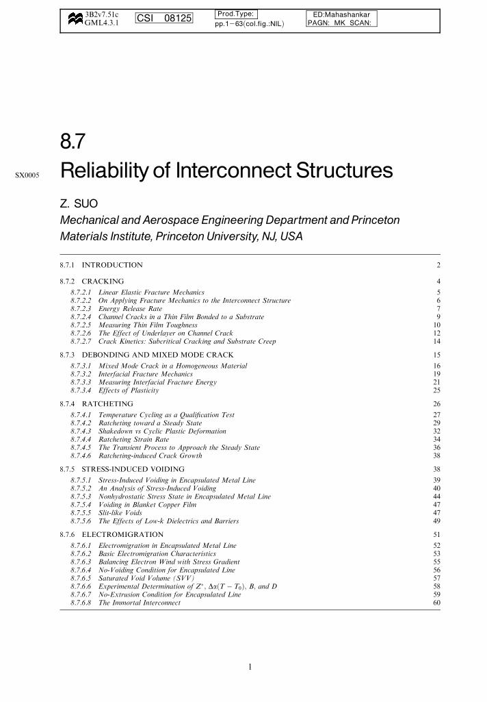
Ever since, the technology has advanced byminiaturization, squeezing more and moretransistors on every single chip. By necessitythe interconnect structure has complex archi-tectures, diverse materials, and small featuresizes. Figure 1 shows a transmission electronmicroscope image of an interconnect structure.The structure is a three-dimensional network
of conductor lines embedded in a dielectricmatrix, fabricated on the silicon surface thatcontains the active devices. The conductor linesare on several levels, and linked by vias. Thelines have rectangular cross-sections and, on agiven level, have a constant thickness butvariable widths. A silicon nitride film caps theinterconnect structure, serving as a barrier ofthe environmental molecules. Lithographicallydefined feature sizes, such as linewidth and viasize, are as small as 100 nm. Films as thin as afew nanometers are used.
Traditional interconnect structures use alu-minum as the conductor, and silica as thedielectric. Tungsten vias link the lines betweenthe levels, and titanium nitride thin layers liebetween the aluminum lines and the dielectric.To make faster devices, the conductor musthave higher conductivity, and the dielectricmust have lower dielectric constant. Copperhas been used as the conductor lines in morerecent interconnect structures (bib104 Rosen-berg et al., 2000). The conductor lines atdifferent levels are linked with copper vias.Liners such as tantalum lie between theconductor and the dielectric to prevent copperdiffusion into the dielectric and to promoteadhesion. Low-dielectric-constant materials ofcurrent use include an organic material knownas SiLK (bib88 Martin et al., 2000), and acarbon doped oxide. The former is ductile, and
Figure 1 A transmission electron microscope image of a cross-section of an interconnect structure (courtesyof John Mardinly, Intel Corporation).
SX0010
SX0015
SX0020
2 Reliability of Interconnect Structures
CSI : 08125
the latter is brittle. Both are compliantcompared to silicon dioxide. To further reducethe dielectric constant, other materials, includ-ing porous materials, will be used in futureinterconnects (bib93 Morgen et al., 1999).
The Monolithic Idea solves one problem,but creates another. Making reliable intercon-nect structures has been a persistent challenge.Stress results from material deposition, thermalexpansion mismatch, and electromigration.Material deposition inevitably generates stress;e.g., deposition of refractory metals such astungsten usually generates stress in the GParange. Materials in interconnect structures,selected to function as conductors, dielectrics,or barriers, have dissimilar thermal expansioncoefficients. On cooling from the fabricationtemperature, the structures acquire stresses. Tofit into the small space, each conductor linemust have a small cross-sectional area. Theintense electric current motivates metal atomsto diffuse in the line, generating tension whereatoms deplete, and compression where atomsaccumulate.
The study of interconnect reliability has along history. Electromigration has been apersistent concern ever since integrated circuitswere mass-produced (bib16 Blech and Meier-an, 1967). As atoms diffuse, voids grow andsever metal lines. Stress-induced voiding wasobserved in the 1980s, when the technologybrought the linewidth comparable to the linethickness (bib24 Curry et al., 1984). Such analuminum line, of approximately square cross-section, encapsulated in silica, develops triaxialstresses of magnitude much above the yieldstrength of aluminum (bib64 Jones and Base-hore, 1987). Voids grow to relax the stresses,facilitated by atomic diffusion (bib106 Sauterand Nix, 1992; bib69 Korhonen et al., 1993).Around the same time, thin film fracturemechanics was advanced (bib30 Evans et al.,1988; bib61 Hutchinson and Suo, 1991; bib124Thouless, 1991), providing tools to quantifytoughness of thin films (bib85 Ma et al., 1998;bib23 Cook and Liniger, 1999), and adhesionbetween thin films (bib25 Dauskardt et al.,1998; bib132 Volinsky et al., 2002). The toolshave been incorporated into industrial practicein material selection, process control, andfailure analysis.
More recently, a new failure mechanism hasbeen identified, in which cracks grow in brittlefilms under cyclic temperatures, aided byratcheting deformation in a metal underlayer(bib57 Huang et al., 2000). Stress-inducedvoiding has been observed in blanket copperfilms (bib109 Shaw et al., 2001; bib107Sekiguchi et al., 2001), and in copper vias inthe copper/silica interconnect structure (bib47
Hommel et al., 2001; bib96 Ogawa et al., 2002).Low dielectric constant materials have lowstiffness; their effects on interconnect reliabilityare the focus of current studies (bib75 Lee et al.,2002; bib4 Ambrico et al., 2002; bib78 bib79Liang et al., 2002a, 2002b; bib102 Rim et al.,2002).
This chapter is organized according to fail-ure modes: cracking, debonding, ratcheting,voiding, and electromigration. Such perversi-ties are not only nuisances—problems to betested away by trial-and-error, but also oppor-tunities for fundamental study of the mechan-ical behavior of diverse materials, in integratedstructures, at an unprecedented small size scale.The study of electromigration has led to thediscovery that adding a few percent of copperinto aluminum interconnects slows aluminumdiffusion rate by nearly two orders of magni-tude. As of early 2000s, the atomistic origin ofthis behavior is still not fully understood. Theobservation of stress-induced voiding, perhapsmore than any other single event, has moti-vated academic researchers to join their in-dustrial colleagues to study atomistic processesof stress generation and relaxation in thinfilms. The introduction of copper and low-dielectric-constant materials has given a newurgency to study cracking and debonding insmall structures. The fundamental study willimpact other major technologies, such asMEMS, integrated photonics, and thermalbarrier coatings, where small-structure me-chanical behavior is important. bib131 Vinciand Baker (2002) have edited a multi-authorreview on mechanical properties in smalldimensions.
The present (our context is early 2000s)method to design reliable small structures, ifthere is one, rests on continuum mechanics,manifest in handbook solutions, commercialfinite element codes, and related measurementprotocols. Their inadequacy is increasinglyevident when the structures become small,because (among other issues) plastic flowsbecome discrete, and failure phenomena be-come nucleation, rather than growth, con-trolled. In the rapidly changing economics oftools for the small, the division of labor has yetbeen settled: what to understand, what tocompute, and what to measure. The tensionbetween the relentless trend of miniaturizationand the disquieting lack of a method to designfor reliability will inspire innovations for yearsto come.
SX0025
SX0030
SX0035
SX0040
SX0045
Introduction 3
CSI : 08125
8.7.2 CRACKING
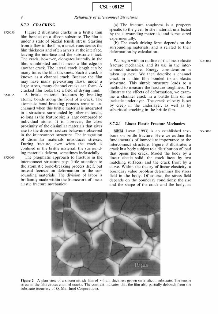
Figure 2 illustrates cracks in a brittle thinfilm bonded on a silicon substrate. The film isunder a state of biaxial tensile stress. Startingfrom a flaw in the film, a crack runs across thefilm thickness and often arrests at the interface,leaving the interface and the substrate intact.The crack, however, elongates laterally in thefilm, uninhibited until it meets a film edge oranother crack. The lateral crack length can bemany times the film thickness. Such a crack isknown as a channel crack. Because the filmmay have many pre-existing flaws, under alarge stress, many channel cracks can form. Acracked film looks like a field of drying mud.
A brittle material fractures by breakingatomic bonds along the front of a crack. Theatomistic bond-breaking process remains un-changed when this brittle material is integratedin a structure, surrounded by other materials,so long as the feature size is large compared toindividual atoms. It is, however, the closeproximity of the dissimilar materials that givesrise to the diverse fracture behaviors observedin the interconnect structure. The integrationof dissimilar materials introduces stresses.During fracture, even when the crack isconfined in the brittle material, the surround-ing materials deform, sometimes inelastcially.
The pragmatic approach to fracture in theinterconnect structure pays little attention tothe atomistic bond-breaking process itself, butinstead focuses on deformation in the sur-rounding materials. The division of labor isbrilliantly made within the framework of linearelastic fracture mechanics:
(a) The fracture toughness is a propertyspecific to the given brittle material, unaffectedby the surrounding materials, and is measuredexperimentally.
(b) The crack driving force depends on thesurrounding materials, and is related to theirdeformation by calculation.
We begin with an outline of the linear elasticfracture mechanics, and its use in the inter-connect structure. Energy consideration istaken up next. We then describe a channelcrack in a thin film bonded to an elasticsubstrate. This simple structure leads to amethod to measure the fracture toughness. Toillustrate the effects of deformation, we exam-ine a channel crack in a brittle film on aninelastic underlayer. The crack velocity is setby creep in the underlayer, as well as bysubcritical cracking in the brittle film.
8.7.2.1 Linear Elastic Fracture Mechanics
bib74 Lawn (1993) is an established text-book on brittle fracture. Here we outline thefundamentals of immediate importance to theinterconnect structure. Figure 3 illustrates acrack in a body subject to a distribution of loadthat opens the crack. Model the body by alinear elastic solid, the crack faces by twomatching surfaces, and the crack front by acurve. Within the theory of linear elasticity, aboundary value problem determines the stressfield in the body. Of course, the stress fielddepends on the boundary conditions: the sizeand the shape of the crack and the body, as
Figure 2 A plan view of a silicon nitride film of B1 mm thickness grown on a silicon substrate. The tensilestress in the film causes channel cracks. The contrast indicates that the film also partially debonds from thesubstrate (courtesy of Q. Ma, Intel Corporation).
SX0050
SX0055
SX0060
SX0061
SX0065
4 Reliability of Interconnect Structures
CSI : 08125

well as the magnitude and the distribution ofthe load. By modeling the crack front as amathematical curve, the linear elasticity theorydoes not account for the atomistic bond-breaking process.
One feature of the stress field, common to allsuch elasticity boundary value problems, playsa special role in the fracture mechanics. Let (r,y) be the polar coordinates, centered at aparticular point along the crack front, in theplane normal to the crack front. The (x1, x2)coordinates are in the same plane. The linearelasticity theory shows that the stress field inthe body takes the form
sijðr; yÞ ¼Kffiffiffiffiffiffiffi2pr
p SijðyÞ: ð1Þ
The dependence on r is square-root singular.The stress field scales with K, known as thestress intensity factor. The factor 2p is intro-duced by convention. The y-dependent func-tions, Sij(y), are listed in bib74 Lawn (1993);for example,
S22ðyÞ ¼ cos ðy=2Þ½1þ sin ðy=2Þsin ð3y=2Þ: ð2Þ
The opening stress a distance r directly aheadof the crack front is
s22ðr; 0Þ ¼Kffiffiffiffiffiffiffi2pr
p : ð3Þ
For a crack in three dimensions, the stressintensity factor K may vary along the front ofthe crack.
The r- and y-dependence of the singularstress field are independent of the boundary
conditions. The boundary conditions, however,do determine the magnitude of the stressintensity factor K. For example, a crack oflength 2a, in an infinite elastic sheet, subject toa tensile stress s remote from the crack, has thestress intensity factor K ¼ s
ffiffiffiffiffiffipa
p: Solutions of
the stress intensity factors for many crackconfigurations are collected in handbooks (e.g.,bib122 Tada et al., 1985). Commercial finiteelement codes are routinely used to calculate Kfor complex crack configurations. Dimensionalconsiderations dictate that the stress intensityfactor should take the form
K ¼ ksffiffiffiffiL
p; ð4Þ
where L is a representative length, s arepresentative stress, and k a dimensionlessnumber. The number k is determined bysolving the boundary value problem. It de-pends on the ratio of the crack length to L, aswell as other ratios that characterize theintegrated structure. Examples will be givenlater.
As mentioned above, the theory of elasticitypredicts that the stress field is square-rootsingular. Of course, we do not believe that thestress is infinite at the crack front. The physicalsignificance of the singular stress field isunderstood as follows (Figure 4). Imagine theplane normal to the crack front. The stress field(1) is valid in an annulus, with the inner radiuslarger than the zone in which the bond-break-
Figure 3 A crack in a body subject to a distributionof load that opens the crack. Also shown is thecoordinate system in a plane normal to the crackfront. Figure 4 The singular stress field is valid in the K-
annulus. Inside the inner circle, the atomistic bond-breaking process invalidates the linear elasticitytheory. Outside the outer circle, the boundaryconditions invalidate the singular stress field.
SX0070
SX0075
SX0080
Cracking 5
CSI : 08125
ing process invalidates the linear elasticitytheory, and the outer radius smaller than thesize of the body and the crack. We call thisannulus the K-annulus. Neither the bond-breaking processes inside the inner circle, northe boundary conditions outside the outercircle affect the r- and y-dependence of thestress field in the K-annulus: the stress field (1)is valid in this annulus. For a brittle solid, thebond-breaking processes invalidate the linearelasticity theory within a zone about 1 nm. Arepresentative feature size in interconnectstructures is 100 nm. These lengths roughlyset the size of the K-annulus.
So far the model does not account for theatomistic bond-breaking process. Imagine twosamples of the same solid, each containing acrack under an opening load. The two samplesmay have different sizes and shapes. The loadson the two samples may also be different.Regardless of such differences, because thestress field in the K-annulus depends on theboundary conditions through the stress inten-sity factor, the bond-breaking processes in thetwo samples must be identical if K is the samefor the two samples. That is, K is the onlymessenger between the external boundaryconditions and the bond-breaking process.
The central idea of the linear elastic fracturemechanics has been so summarized: the sameK, the same crack-tip process. Within thefracture mechanics, the simplest way to ac-count for the bond-breaking process is tostipulate that the crack extends when the stressintensity factor K in a body containing a crackreaches a critical value, Kc, known as thefracture toughness.
Once the stress intensity factor is calculatedfor a given crack configuration, in the form of(4), the condition for the crack to grow is
ksffiffiffiffiL
p¼ Kc: ð5Þ
For a given material, the fracture toughnessis determined experimentally. Start with aspecimen of the material, introduce a crackinto the sample, load the sample until the crackextends, and record the critical load. Indepen-dently solve the elasticity boundary valueproblem, and obtain the stress intensity factorin the form (4). The experimentally measuredcritical load then gives the fracture toughness.The fracture toughness is a material property,which is independent of the sample geometryand load. The stress intensity factor is aloading parameter, which does depend on thesample geometry and the load.
8.7.2.2 On Applying Fracture Mechanics tothe Interconnect Structure
bib82 Liu et al. (2000) have discussed the useof fracture mechanics to formulate design rulesfor the interconnect structure. For example,assume that the representative stress is set bythe thermal mismatch between two materials.The length L can be set to be a feature size,such as film thickness or via diameter. Tocompute k, one needs to place a crack in thestructure, and know its location, orientation,and size. Such information is never availablefor a complex structure. A pragmatic approachis to place cracks in the structure hypotheti-cally. For the interconnect structure, thefabrication process controls the structure tothe feature size, so that the crack size shouldnot exceed the feature size. Ideally, one wishesto find the worst crack that gives the largeststress intensity factor. In practice, one doescalculations for a few representative cracks.Because such an approach is time consuming,broad conclusions drawn from idealized struc-tures are particularly valuable.
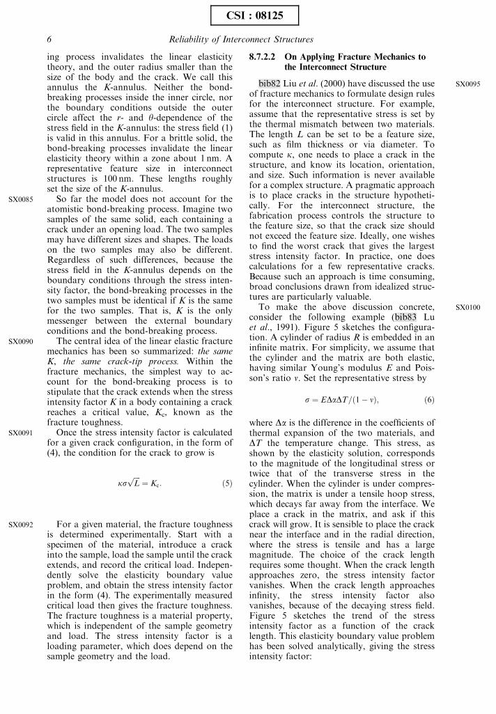
To make the above discussion concrete,consider the following example (bib83 Luet al., 1991). Figure 5 sketches the configura-tion. A cylinder of radius R is embedded in aninfinite matrix. For simplicity, we assume thatthe cylinder and the matrix are both elastic,having similar Young’s modulus E and Pois-son’s ratio n. Set the representative stress by
s ¼ EDaDT=ð1� nÞ; ð6Þ
where Da is the difference in the coefficients ofthermal expansion of the two materials, andDT the temperature change. This stress, asshown by the elasticity solution, correspondsto the magnitude of the longitudinal stress ortwice that of the transverse stress in thecylinder. When the cylinder is under compres-sion, the matrix is under a tensile hoop stress,which decays far away from the interface. Weplace a crack in the matrix, and ask if thiscrack will grow. It is sensible to place the cracknear the interface and in the radial direction,where the stress is tensile and has a largemagnitude. The choice of the crack lengthrequires some thought. When the crack lengthapproaches zero, the stress intensity factorvanishes. When the crack length approachesinfinity, the stress intensity factor alsovanishes, because of the decaying stress field.Figure 5 sketches the trend of the stressintensity factor as a function of the cracklength. This elasticity boundary value problemhas been solved analytically, giving the stressintensity factor:
SX0085
SX0090
SX0091
SX0092
SX0095
SX0100
6 Reliability of Interconnect Structures
CSI : 08125
K
sffiffiffiffiR
p ¼ p8
� �1=2 a
R
� �1þ a
R
� ��3=2
: ð7Þ
If we can estimate the largest flaw sizepossible due to a certain fabrication process,we can set the crack size to this flaw size, andthen calculate the stress intensity factor. If weknow nothing about the flaw, we may proceedas follows. The stress intensity factor (7) attainsa maximum, Kmax ¼ 0:24s
ffiffiffiffiR
p; at a/R¼ 0.5.
No matrix flaw can grow provided thismaximum stress intensity factor is below thefracture toughness, namely,
0:24EDaDT
1� n
ffiffiffiffiR
poKc: ð8Þ
This condition invokes well-defined quanti-ties, and does not rely on any knowledge of theflaw. Everything else being equal, a cylinderwith a smaller radius is less likely to causematrix cracking. Assuming s¼ 1GPa andKc ¼ 1 MPa m1=2; condition (8) gives thecritical radius Rc¼ 17 mm.
8.7.2.3 Energy Release Rate
Additional insight is gained by analyzing theelastic energy change associated with crackextension. Once again, consider the crack, areaA, in an elastic body, subject to a distributionof load that opens the crack. Let F representthe magnitude of the load, and D the displace-
ment, such that when D changes by dD, theload does work F dD to the body. Let U be theelastic energy stored in the body. When thedisplacement varies, but the crack area remainsfixed, the work done by the load equals thechange in the elastic energy of the body,namely, dU¼F dD when dA¼ 0. The elasticenergy U is represented by the area under theload–displacement curve (Figure 6(a)).
Imagine two copies of the body, identical inall respect except for a small difference in thecrack areas. The copy with the larger crack ismore compliant and, at the same displacement,stores lower elastic energy (Figure 6(b)).Regard the elastic energy stored in the bodyas a function of the displacement and the crackarea, U(D, A). Define energy release rate, G, asthe reduction of the elastic energy associatedwith the crack increasing per unit area, whenthe external load does no work, namely,
G ¼ � qUðD;AÞqA
: ð9Þ
The partial derivative signifies that the dis-placement D is held fixed when the crack area Avaries. For a given crack configuration, onecan solve the elasticity boundary value pro-blem, compute the elastic energy stored in thebody, U(D, A), and then obtain the energyrelease rate G.
The above definition is still sloppy. Ingeneral, the energy release rate varies alongthe crack front. Denote the curved coordinatealong the crack front by s, and the energy
Figure 5 A cylinder is embedded in a matrix. The cylinder is under compression. The tensile hoop stress inthe matrix causes cracking. The stress intensity factor is plotted as a function of the crack length.
SX0105
SX0106
SX0110
SX0115
SX0120
Cracking 7
CSI : 08125

release rate is a function G(s). Imagine a bodysubject to a fixed displacement D. The elasticenergy stored in the body is a function of thecrack shape, as well as the crack area. Let thecrack advance by a small length da, which canvary along the crack front. Associated with thechange in the crack, the elastic energy stored inthe body varies by dU. Define the energyrelease rate such that
dU ¼ �Z
GðsÞ da ds: ð10Þ
The integral extends along the entire crackfront. In what follows, we will mostly overlook
this detail, and assume that the energy releaserate is uniform along the crack front.
When both the displacement and the crackarea vary, the elastic energy varies according to
dU ¼ F dD� G dA: ð11Þ
The elastic energy is a function of thedisplacement and the crack area, U(D, A).The load F and the energy release rate G arethe differential coefficients. Just as F is theforce conjugate to the displacement D, theenergy release rate G is the force conjugate tothe crack area A. Such a force is known as aconfigurational force.
Define the potential energy as P¼U–FD.Write Equation (11) in a different form:
dP ¼ �D dF � G dA: ð12Þ
Now the potential energy is a function of theload and the crack area, P(F,A). The displace-ment D and the energy release rate G are thedifferential coefficients. Equation (12) suggestsan equivalent definition of the energy releaserate:
G ¼ � qPðF ;AÞqA
: ð13Þ
The partial derivative signifies that the load F isheld fixed when the crack area A varies. Whenthe body is linearly elastic, U¼FD/2 and P¼ –U, so that (13) becomes
G ¼ þqUðF ;AÞqA
: ð14Þ
The partial derivative signifies that the load F isheld fixed when the crack area A varies. Thesign difference in Equations (9) and (14)reflects a simple physical fact. When the crackarea is larger, the body is more compliant, sothat the body stores less elastic energy at afixed displacement, but stores more elasticenergy at a fixed load.
It has been shown that the energy releaserate relates to the stress intensity factor as
G ¼ K2
%E; ð15Þ
where %E ¼ E under the plane stress condition,and %E ¼ E=ð1� n2Þ under the plane strainconditions. Here E is Young’s modulus, and nPoisson’s ratio. Fracture mechanics has beenformulated either in terms of the stressintensity factor, or the energy release rate.The two formulations are equivalent. Bothcontribute to the understanding of the fracturemechanics. The simplest fracture condition isthat the crack advances when the energy
Figure 6 (a) When the crack is stationary in anelastic body, the load is linear in the displacement.The area under the curve represents the elasticenergy stored in the body. (b) For the two copies ofthe elastic body, each containing a stationary crack,the body with a larger crack area (A2) has a largercompliance.
SX0121
SX0125
SX0130
8 Reliability of Interconnect Structures
CSI : 08125

release rate attains a critical value, G, known asthe fracture energy. Obviously, the fractureenergy relates to the fracture toughness as G ¼K2
c = %E:
8.7.2.4 Channel Cracks in a Thin Film Bondedto a Substrate
In an interconnect structure, often a crackruns in one material, but the neighboringmaterial remains intact and exerts a constrainton the crack. Figure 7 illustrates two structuresfor comparison. In Figure 7(a), a crack oflength a, in a freestanding sheet of thickness h,is subject to a tensile stress s remote from thecrack. Assume that the displacement at theload point is fixed, so that the load does nowork when the crack extends. When the crackis introduced, the stress near the crack faces ispartially relieved. The volume in which thestress relaxes scales as a2h, so that relative tothe uncracked, stressed sheet, the elastic energyin the cracked sheet changes by DUB–a2hs2/E.Consequently, GBas2/E, namely, the energyrelease rate for a crack in a freestanding sheetincreases with the crack length.
Figure 7(b) illustrates a thin elastic filmbonded to an elastic substrate. When the cracklength a is much larger than the film thicknessh, the stress field in the crack wake becomesinvariant as the crack extends. The volume inwhich the stress relaxes scales as ah2, so thatthe introduction of the crack changes theelastic energy by DUB� ah2s2=Ef : The energyrelease rate is
G ¼ Zs2h
%Ef
: ð16Þ
The dimensionless number Z depends on theelastic constants of the film and the substrate.The number must be determined by solving theboundary value problem. When the thin filmand the substrate have similar elastic constants,Z¼ 2.0. bib11 Beuth (1992) calculated the Zvalues for a thin film on an infinite substratewith dissimilar elastic constants. When thesubstrate is stiffer than the film, Z is between 1and 2. When the substrate is much morecompliant than the film, Z can be very large.
For the channel crack, the energy releaserate scales with the film thickness, and isindependent of the crack length when thecrack length exceeds several times the filmthickness (bib3 Ambrico and Begley, 2002).Take Z¼ 2, s¼ 109 Pa, %Ef ¼ 1011 Pa; andG¼ 10 Jm�2. Equating the energy release rateG in (16) to the fracture energy G, we find acritical film thickness hc¼ 0.5 mm. Channelcracks can propagate in films thicker than hc,but not in films thinner than hc.
bib138 Ye et al. (1992) have shown that thechannel crack energy release rate increases ifthe crack can dip into the substrate, or the filmand substrate can debond. bib4 Ambrico et al.(2002) have studied channel cracks multilayerswith lateral patterning, with particular refer-ence to interconnects consisting of copper andlow-k dielectrics. Using the extended finiteelement method (XFEM), bib58 Huang et al.(2003) have studied the effects of substratethickness and channel spacing, with particularattention to compliant substrates.
Figure 7 (a) A crack in a freestanding sheet and (b) a channel crack in a thin film bonded to a substrate.
SX0135
SX0140
SX0145
SX0150
Cracking 9
CSI : 08125
8.7.2.5 Measuring Thin Film Toughness
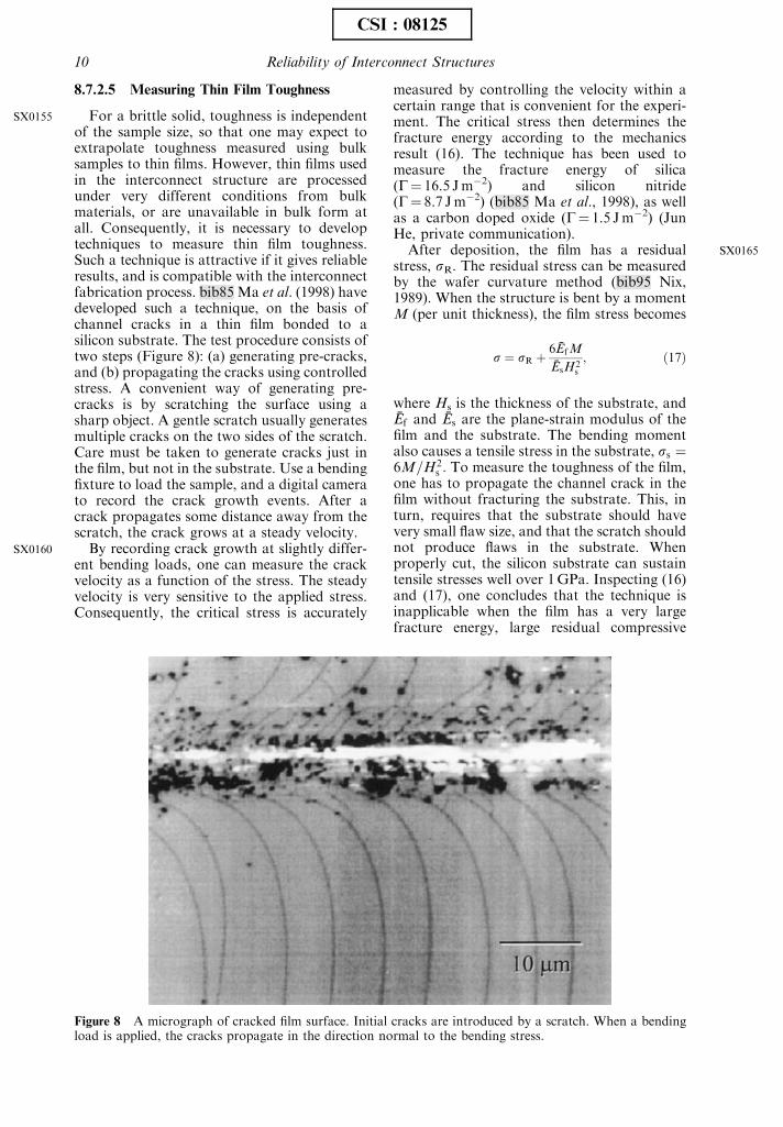
For a brittle solid, toughness is independentof the sample size, so that one may expect toextrapolate toughness measured using bulksamples to thin films. However, thin films usedin the interconnect structure are processedunder very different conditions from bulkmaterials, or are unavailable in bulk form atall. Consequently, it is necessary to developtechniques to measure thin film toughness.Such a technique is attractive if it gives reliableresults, and is compatible with the interconnectfabrication process. bib85 Ma et al. (1998) havedeveloped such a technique, on the basis ofchannel cracks in a thin film bonded to asilicon substrate. The test procedure consists oftwo steps (Figure 8): (a) generating pre-cracks,and (b) propagating the cracks using controlledstress. A convenient way of generating pre-cracks is by scratching the surface using asharp object. A gentle scratch usually generatesmultiple cracks on the two sides of the scratch.Care must be taken to generate cracks just inthe film, but not in the substrate. Use a bendingfixture to load the sample, and a digital camerato record the crack growth events. After acrack propagates some distance away from thescratch, the crack grows at a steady velocity.
By recording crack growth at slightly differ-ent bending loads, one can measure the crackvelocity as a function of the stress. The steadyvelocity is very sensitive to the applied stress.Consequently, the critical stress is accurately
measured by controlling the velocity within acertain range that is convenient for the experi-ment. The critical stress then determines thefracture energy according to the mechanicsresult (16). The technique has been used tomeasure the fracture energy of silica(G¼ 16.5 Jm�2) and silicon nitride(G¼ 8.7 Jm�2) (bib85 Ma et al., 1998), as wellas a carbon doped oxide (G¼ 1.5 Jm�2) (JunHe, private communication).
After deposition, the film has a residualstress, sR. The residual stress can be measuredby the wafer curvature method (bib95 Nix,1989). When the structure is bent by a momentM (per unit thickness), the film stress becomes
s ¼ sR þ 6 %EfM
%EsH2s
; ð17Þ
where Hs is the thickness of the substrate, and%Ef and %Es are the plane-strain modulus of thefilm and the substrate. The bending momentalso causes a tensile stress in the substrate, ss ¼6M=H2
s : To measure the toughness of the film,one has to propagate the channel crack in thefilm without fracturing the substrate. This, inturn, requires that the substrate should havevery small flaw size, and that the scratch shouldnot produce flaws in the substrate. Whenproperly cut, the silicon substrate can sustaintensile stresses well over 1GPa. Inspecting (16)and (17), one concludes that the technique isinapplicable when the film has a very largefracture energy, large residual compressive
Figure 8 A micrograph of cracked film surface. Initial cracks are introduced by a scratch. When a bendingload is applied, the cracks propagate in the direction normal to the bending stress.
SX0155
SX0160
SX0165
10 Reliability of Interconnect Structures
CSI : 08125

stress, small thickness, or low modulus. In theexperiment of bib85 Ma et al. (1998), a thinmetal layer is deposited on the silicon sub-strate, and the brittle film is deposited on themetal. The metal layer serves as a barrierpreventing the crack from entering the sub-strate. The metal layer, upon yielding, alsoincreases the energy release rate for a givenbending moment (Section 8.7.2.6).
One may also greatly amplify the energyrelease rate for a given stress by using thestructure in Figure 9. The cavity underneaththe brittle film may be made by MEMSfabrication method. When the crack grows,the stress in the film is relaxed, and the energyrelease rate,
G ¼ s2L
%Ef
; ð18Þ
now scales with the length of the cavity, ratherthan the film thickness.
8.7.2.6 The Effect of Underlayer on ChannelCrack
When a brittle film is bonded to a plasticallydeformable substrate, the constraint of the
substrate on the crack in the film is partiallylost. In the limiting case, when the yieldstrength of the substrate is much below thestress in the film, the film is equivalent to afreestanding sheet. Consequently, the plasticdeformation in the substrate encourages thechannel cracks in the film. This effect has beenstudied by bib54 Hu and Evans (1989) by usinga shear lag model, by bib12 Beuth andKlingbeil (1996) for a brittle film on a semi-infinite elastic–plastic substrate, and by bib3Ambrico and Begley (2002) for a brittle film ona ductile underlayer. In this section, using ashear lag model, we (bib118 Suo and He, 2002)examine the structure depicted in Figure 10,consisting of an overlayer, an underlayer, and asubstrate. The crack cuts across the overlayer,with the crack root arresting at the interfacebetween the overlayer and the underlayer. Theoverlayer is taken to be elastic, and thesubstrate is rigid. The property of the under-layer will be varied to study its effect on thechannel crack.
The overlayer may consist of multiple brittlefilms. The stress in the overlayer is a functionof the position through the thickness, s(z).Define the membrane force in the overlayer by
Figure 10 A structure consists of an elastic overlayer, an elastic–plastic underlayer, and a rigid substrate.
Figure 9 When the film is above a wide cavity, the crack driving force increases greatly.
SX0170
SX0175
SX0180
Cracking 11
CSI : 08125
N ¼Z
sðzÞ dz: ð19Þ
The integral extends over the thickness of theoverlayer. Similarly, define the membranestiffness by
B ¼Z
%EðzÞ dz; ð20Þ
where %EðzÞ is the plane strain modulus of thematerial at z.
We now consider the wake of the crack inthe overlayer on a ductile underlayer. Whenthe overlayer is uncracked, subject to amembrane force NN, uniform in the plane ofthe layer, the displacement field in the over-layer is set to be zero. Relative to this referencestate, the overlayer deforms when a crack isintroduced. Let u(x) be the displacement fieldaveraged across the thickness of the overlayer.On the interface, the overlayer and the under-layer interact with each other through the shearstress field t(x). We model the underlayer as atime-independent elastic plastic material, witha nonlinear relation between the shear stress tand the displacement u.
When a crack cuts across the thickness of theoverlayer at x¼ 0, the membrane force in theoverlayer, N(x), varies with the position,having the boundary conditions N(0)¼ 0 andN(N)¼NN. Hooke’s law relates the mem-brane force to the displacement gradient:
NðxÞ ¼ NN þ Bdu
dx: ð21Þ
The force balance of an element of the over-layer requires that
dN
dx¼ t: ð22Þ
Inserting (21) into (22), we obtain the ordinarydifferential equation for u(x):
Bd2u
dx2¼ tðuÞ: ð23Þ
Multiplying (23) by du/dx, and integratingfrom x¼ 0 to x¼N, we obtain that
N2N
2B¼
Z u0
0
tðuÞ du: ð24Þ
In reaching the above equation, we have usedthe following boundary conditions: u¼ u0 anddu/dx¼ –NN/B at x¼ 0, and u¼ 0 and du/dx¼ 0 at x¼N. When the underlayer prop-erty t(u) is known, (24) provides the relationbetween the crack opening displacement u0 and
the membrane force NN in the uncrackedoverlayer.
For a multi-material overlayer, the energyrelease rate depends on the position, G(z). Theintegral
f ¼Z
G dz ð25Þ
gives the elastic energy change associated withthe crack advancing per unit length in theoverlayer. The quantity f has the unit of force,and is the driving force for the channel crack.
The channel driving force is given by thecomplementary energy integral (bib12 Beuthand Klingbeil, 1996):
f ¼ 2
Z NN
0
u0 dNN: ð26Þ
Once the u0–NN relation is obtained from (24),the driving force for the channel crack iscalculated from (26).
We next list solutions for idealized materiallaw, t(u). We assume that the underlayer hasthe uniform property, and the shear stress isconstant across the thickness of the underlayer.Consequently, the shear strain g is also con-stant across the thickness of the underlayer.The shear strain relates to the overlayerdisplacement as g(x)¼ u(x)/H, where H is thethickness of the underlayer.
Elastic underlayer. The underlayer is linearelastic with shear modulus m, so that t¼ mu/H.Integrating (24), we obtain the u0–NN relation
u0 ¼ NN
ffiffiffiffiffiffiH
mB
s: ð27Þ
Integrating (26) gives the driving force for thecrack in the overlayer:
f ¼ N2N
ffiffiffiffiffiffiH
mB
s: ð28Þ
This result reproduces that obtained by bib141Xia and Hutchinson (2000). As expected, thecrack driving force is quadratic in the mem-brane force. At a given membrane force, thecrack driving force is large when the underlayeris thick and compliant. This result is applicableto, for example, a nitride passivation film on acomplaint dielectric layer. As the microelec-tronic industry implements low-dielectric-con-stant materials, with accompanying low
SX0190
SX0191
SX0195
SX0200
SX0205
SX0210
SX0215
12 Reliability of Interconnect Structures
CSI : 08125
stiffness, the likelihood of cracking in thebrittle passivation film will increase.
Rigid, perfect plastic underlayer. Neglectelasticity of the film, and assume that theunderlayer deforms plastically at a constantstress t¼ tY. Integrating (24), we obtain theu0–NN relation
u0 ¼N2
N
2BtY: ð29Þ
Inserting into (26) gives driving force for thecrack in the overlayer:
f ¼ N3N
3BtY: ð30Þ
This reproduces the result of bib54 Hu andEvans (1989). The crack driving force is cubicin the membrane force, inversely proportionalto the underlayer yield strength, and indepen-dent of the underlayer thickness.
Elastic, perfectly plastic underlayer. The filmnow has the shear modulus m, the yield strengthtY, and the yield strain gY¼ tY/m. Whenu0ogYH, the film is elastic, and (27) providesthe u0–NN relation. When u04gYH, a segmentof the film near the crack deforms plastically,and the film fare from the crack is still elastic.Using (27), we write the yield condition interms of the membrane force:
NNffiffiffiffiffiffiffiffiffiffiffiffiffiffiffiffiffiffitYgYHB
p ¼ 1: ð31Þ
Integrating (24), we obtain the opening dis-placement of the crack wake
u0
gYH¼ 1
2þ 1
2
NNffiffiffiffiffiffiffiffiffiffiffiffiffiffiffiffiffiffitYgYHB
p� �2
: ð32Þ
This is the u0–NN relation whenNN=
ffiffiffiffiffiffiffiffiffiffiffiffiffiffiffiffiffiffitYgYHB
p41; for smaller NN, the film
is elastic, and the u0–NN relation is given by(27). Inserting the whole u0–NN relation into(26), we find the driving force for the crack inthe overlayer:
f ¼ N3N
3BtY1� NNffiffiffiffiffiffiffiffiffiffiffiffiffiffiffiffiffiffi
tYgYHBp
� ��3"
þ3NNffiffiffiffiffiffiffiffiffiffiffiffiffiffiffiffiffiffi
tYgYHBp
� ��2#
ð33Þ
When NN=ffiffiffiffiffiffiffiffiffiffiffiffiffiffiffiffiffiffitYgYHB
p ¼ 1; the underlayer iselastic, and (33) recovers (28). WhenNN=
ffiffiffiffiffiffiffiffiffiffiffiffiffiffiffiffiffiffitYgYHB
pc1; the two terms in the
bracket is negligible, and (33) recovers theresult for the rigid perfect plastic case (30).
Power-law plastic underlayer. Now we as-sume that the film deforms according to thepower law
ttY
¼ u
HgY
� �n
; ð34Þ
where tY is an arbitrarily selected referencestress, and gY and n are parameters used to fitexperiment data. Following the same proce-dure as before, we obtain the u0–NN relation
u0
gYH¼ ðn þ 1ÞN2
N
2tYgYHB
�1=ðnþ1Þ
; ð35Þ
and the crack driving force
f ¼ 2gYH
n þ 3
ðn þ 1Þnþ2Nnþ3
N
2BHtYgY
" #1=ðnþ1Þ
: ð36Þ
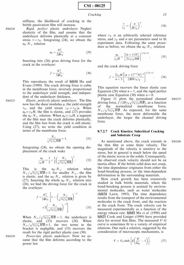
This equation recovers the linear elastic caseEquation (28) when n¼ 1, and the rigid perfectplastic case Equation (30) when n¼ 0.
Figure 11 plots the normalized channeldriving force, f =ðHgY
ffiffiffiffiffiffiffiffiffiffiffiffiffiffiffiffiffiffitYgYHB
pÞ; as a function
of the normalized membrane force,NN=
ffiffiffiffiffiffiffiffiffiffiffiffiffiffiffiffiffiffitYgYHB
p: As expected, for the same
membrane force, the more deformable theunderlayer, the larger the channel drivingforce.
8.7.2.7 Crack Kinetics: Subcritical Crackingand Substrate Creep
As mentioned above, the crack extends inthe thin film at some finite velocity. Themagnitude of the velocity is sensitive to thestress, but in general is much below the speedof the elastic waves in the solids. Consequently,the observed crack velocity should not be aninertia effect. If the brittle solid does not creep,the time dependence originates from either thebond-breaking process, or the time-dependentdeformation in the surrounding materials.
Slow crack growth has been extensivelystudied in bulk brittle materials, where thebond-breaking process is assisted by environ-mental molecules, such as water molecules(bib74 Lawn, 1993). The time dependenceresults from the transport of the environmentalmolecules to the crack front, and the reactionat the crack front. The crack velocity can bemeasured experimentally as a function of theenergy release rate. bib85 Ma et al. (1998) andbib23 Cook and Liniger (1999) have provideddata for several thin films. The measured V–Gcurve is sometimes fit to a variety of empiricalrelations. One such a relation, suggested by theconsideration of microscopic mechanisms, is
V ¼ V0 sinh bG
Gth� 1
� � �; ð37Þ
SX0220
SX0225
SX0230
SX0235
SX0240
SX0245
Cracking 13
CSI : 08125
where V0, Gth and b are parameters to fitexperimental data.
I owe Dr. Jun He, of Intel Corporation, forthe following idea. The V–G curve is specific tothe brittle material and the environment, but isindependent of the surrounding materials, ifthey do not prevent the environmental mole-cules from reaching the crack front. The V–Gcurve for a given material can be measuredusing a simple structure, such as a film on asilicon substrate. When the brittle material is ina more complex structure, the same V–G stillapplies. Because the crack velocity is readilymeasurable, the measured crack velocity, to-gether with the known V–G curve, determinesthe energy release rate. The method is accuratebecause the crack velocity sensitively dependson the energy release rate. As we have seen inFigure 11, the energy release rate is affected bythe deformation behavior of the surroundingmaterials. Direct measurements of G provide ameans to study the deformation behavior ofthe surrounding materials.
The crack velocity is also affected if thesurrounding materials creep. As an example,consider the structure illustrated in Figure 10again, now assume that the underlayer isviscous (bib78 Liang et al., 2002a). Initially,the film is in a uniform biaxial tensile stressstate s. When the underlayer creeps, the stressfield in the film relaxes in the crack wake, butintensifies around the crack tip. When the cracktip moves slowly, the crack wake has a long
time to relax, and the stress intensity aroundthe crack tip increases. When the crack tipmoves rapidly, the crack wake has a short timeto relax, and the stress intensity around thecrack tip decreases. Consequently, the crackcan attain a steady velocity, given by
V ¼ 0:6Hhs2
ZG: ð38Þ
As expected, the larger the steady velocity,the smaller the energy release rate. If the film issusceptible to subcritical crack growth, one canseparately determine the V–G curve of thematerial, e.g., using the film on an elasticsubstrate. Once the crack velocity V is mea-sured for the film on the viscous underlayer,one can read the energy release rate G form theV–G curve. The measured V and G, togetherwith Equation (38), provide a means todetermine the viscosity of the underlayer.
8.7.3 DEBONDING AND MIXED MODECRACK
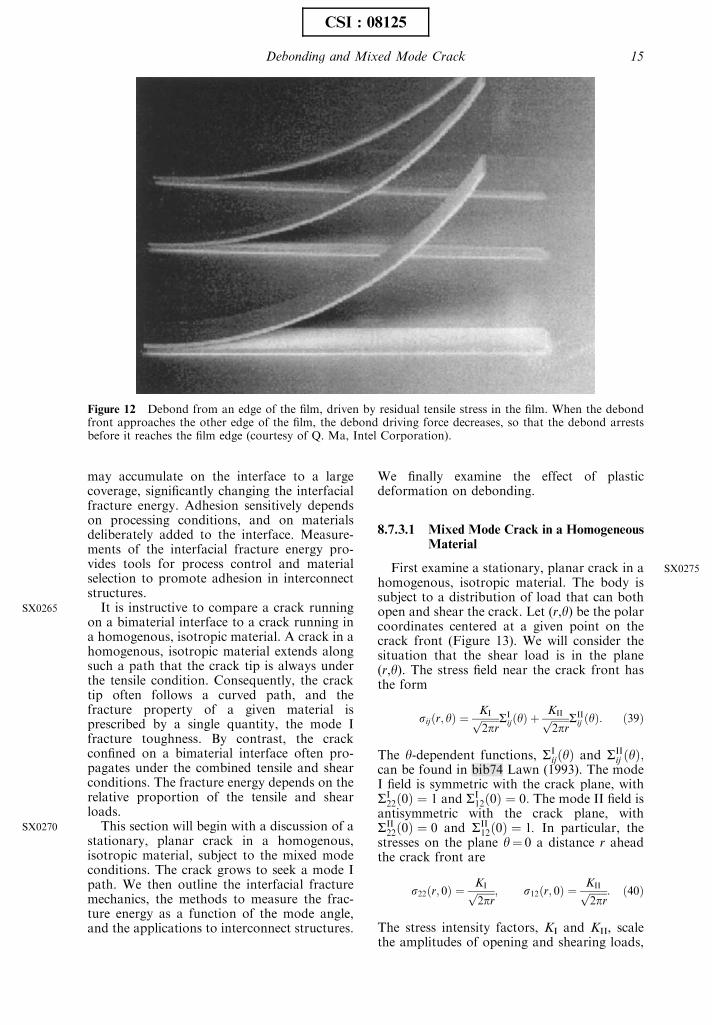
The interconnect structure consists of manydissimilar materials. Debonding has been aprimary concern. Figure 12 is a micrograph ofa thin film debonding from a substrate. Withinthe linear elastic fracture mechanics, we modelthe debond process as a crack extending on theinterface between two elastic materials. Impu-rities, of minute amount by volume fraction,
Figure 11 The driving force for channel crack as a function of the membrane force. Several underlayerbehaviors are compared: elastic, perfectly plastic, elastic–plastic, elastic–perfectly-plastic, and power law.
SX0250
SX0255
SX0256
SX0260
14 Reliability of Interconnect Structures
CSI : 08125
may accumulate on the interface to a largecoverage, significantly changing the interfacialfracture energy. Adhesion sensitively dependson processing conditions, and on materialsdeliberately added to the interface. Measure-ments of the interfacial fracture energy pro-vides tools for process control and materialselection to promote adhesion in interconnectstructures.
It is instructive to compare a crack runningon a bimaterial interface to a crack running ina homogenous, isotropic material. A crack in ahomogenous, isotropic material extends alongsuch a path that the crack tip is always underthe tensile condition. Consequently, the cracktip often follows a curved path, and thefracture property of a given material isprescribed by a single quantity, the mode Ifracture toughness. By contrast, the crackconfined on a bimaterial interface often pro-pagates under the combined tensile and shearconditions. The fracture energy depends on therelative proportion of the tensile and shearloads.
This section will begin with a discussion of astationary, planar crack in a homogenous,isotropic material, subject to the mixed modeconditions. The crack grows to seek a mode Ipath. We then outline the interfacial fracturemechanics, the methods to measure the frac-ture energy as a function of the mode angle,and the applications to interconnect structures.
We finally examine the effect of plasticdeformation on debonding.
8.7.3.1 Mixed Mode Crack in a HomogeneousMaterial
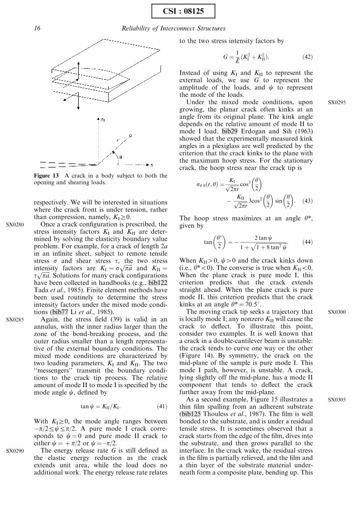
First examine a stationary, planar crack in ahomogenous, isotropic material. The body issubject to a distribution of load that can bothopen and shear the crack. Let (r,y) be the polarcoordinates centered at a given point on thecrack front (Figure 13). We will consider thesituation that the shear load is in the plane(r,y). The stress field near the crack front hasthe form
sijðr; yÞ ¼KIffiffiffiffiffiffiffi2pr
p SIijðyÞ þ
KIIffiffiffiffiffiffiffi2pr
p SIIij ðyÞ: ð39Þ
The y-dependent functions, SIijðyÞ and SII
ij ðyÞ;can be found in bib74 Lawn (1993). The modeI field is symmetric with the crack plane, withSI22ð0Þ ¼ 1 and SI
12ð0Þ ¼ 0: The mode II field isantisymmetric with the crack plane, withSII22ð0Þ ¼ 0 and SII
12ð0Þ ¼ 1. In particular, thestresses on the plane y¼ 0 a distance r aheadthe crack front are
s22ðr; 0Þ ¼KIffiffiffiffiffiffiffi2pr
p ; s12ðr; 0Þ ¼KIIffiffiffiffiffiffiffi2pr
p : ð40Þ
The stress intensity factors, KI and KII, scalethe amplitudes of opening and shearing loads,
Figure 12 Debond from an edge of the film, driven by residual tensile stress in the film. When the debondfront approaches the other edge of the film, the debond driving force decreases, so that the debond arrestsbefore it reaches the film edge (courtesy of Q. Ma, Intel Corporation).
SX0265
SX0270
SX0275
Debonding and Mixed Mode Crack 15
CSI : 08125
respectively. We will be interested in situationswhere the crack front is under tension, ratherthan compression, namely, KIZ0.
Once a crack configuration is prescribed, thestress intensity factors KI and KII are deter-mined by solving the elasticity boundary valueproblem. For example, for a crack of length 2ain an infinite sheet, subject to remote tensilestress s and shear stress t, the two stressintensity factors are KI ¼ s
ffiffiffiffiffiffipa
pand KII ¼
tffiffiffiffiffiffipa
p: Solutions for many crack configurations
have been collected in handbooks (e.g., bib122Tada et al., 1985). Finite element methods havebeen used routinely to determine the stressintensity factors under the mixed mode condi-tions (bib77 Li et al., 1985).
Again, the stress field (39) is valid in anannulus, with the inner radius larger than thezone of the bond-breaking process, and theouter radius smaller than a length representa-tive of the external boundary conditions. Themixed mode conditions are characterized bytwo loading parameters, KI and KII. The two‘‘messengers’’ transmit the boundary condi-tions to the crack tip process. The relativeamount of mode II to mode I is specified by themode angle c, defined by
tan c ¼ KII=KI: ð41Þ
With KIZ0, the mode angle ranges between�p/2rcrp/2. A pure mode I crack corre-sponds to c¼ 0 and pure mode II crack toeither c¼ þ p/2 or c¼ –p/2.
The energy release rate G is still defined asthe elastic energy reduction as the crackextends unit area, while the load does noadditional work. The energy release rate relates
to the two stress intensity factors by
G ¼ 1
%EðK2
I þ K2IIÞ: ð42Þ
Instead of using KI and KII to represent theexternal loads, we use G to represent theamplitude of the loads, and c to representthe mode of the loads.
Under the mixed mode conditions, upongrowing, the planar crack often kinks at anangle from its original plane. The kink angledepends on the relative amount of mode II tomode I load. bib29 Erdogan and Sih (1963)showed that the experimentally measured kinkangles in a plexiglass are well predicted by thecriterion that the crack kinks to the plane withthe maximum hoop stress. For the stationarycrack, the hoop stress near the crack tip is
sy yðr; yÞ ¼KIffiffiffiffiffiffiffi2pr
p cos3y2
� �
� KIIffiffiffiffiffiffiffi2pr
p 3cos2y2
� �sin
y2
� �: ð43Þ
The hoop stress maximizes at an angle y*,given by
tany�
2
� �¼ � 2 tanc
1þffiffiffiffiffiffiffiffiffiffiffiffiffiffiffiffiffiffiffiffiffiffiffiffiffi1þ 8 tan2 c
p : ð44Þ
When KII40, c40 and the crack kinks down(i.e., y*o0). The converse is true when KIIo0.When the plane crack is pure mode I, thiscriterion predicts that the crack extendsstraight ahead. When the plane crack is puremode II, this criterion predicts that the crackkinks at an angle y*¼ 70.51.
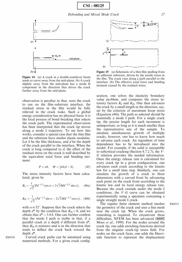
The moving crack tip seeks a trajectory thatis locally mode I; any nonzero KII will cause thecrack to deflect. To illustrate this point,consider two examples. It is well known thata crack in a double-cantilever beam is unstable:the crack tends to curve one way or the other(Figure 14). By symmetry, the crack on themid-plane of the sample is pure mode I. Thismode I path, however, is unstable. A crack,lying slightly off the mid-plane, has a mode IIcomponent that tends to deflect the crackfurther away from the mid-plane.
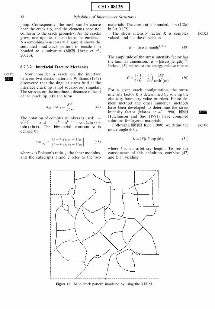
As a second example, Figure 15 illustrates athin film spalling from an adherent substrate(bib125 Thouless et al., 1987). The film is wellbonded to the substrate, and is under a residualtensile stress. It is sometimes observed that acrack starts from the edge of the film, dives intothe substrate, and then grows parallel to theinterface. In the crack wake, the residual stressin the film is partially relieved, and the film anda thin layer of the substrate material under-neath form a composite plate, bending up. This
Figure 13 A crack in a body subject to both theopening and shearing loads.
SX0280
SX0285
SX0290
SX0295
SX0300
SX0305
16 Reliability of Interconnect Structures
CSI : 08125
observation is peculiar in that, were the crackto run on the film–substrate interface, theresidual stress in the film would be fullyrelieved in the crack wake. Such a globalenergy consideration has no physical basis: it isthe local process of bond breaking that selectsthe crack path. The experimental observationhas been interpreted that the crack tip movesalong a mode I trajectory. To see how thisworks, consider a special case that the thin filmand the substrate have similar elastic modulus.Let h be the film thickness, and d be the depthof the crack parallel to the interface. When thecrack is long compared to d, the effect of theresidual stress on the crack is well described bythe equivalent axial force and bending mo-ment:
P ¼ sh; M ¼ 12shðd � hÞ: ð45Þ
The stress intensity factors have been calcu-lated, given by
KI ¼1ffiffiffi2
p ðPd�1=2 cosoþ 2ffiffiffi3
pMd�3=2 sinoÞ; ð46aÞ
KII ¼1ffiffiffi2
p ðPd�1=2 sino� 2ffiffiffi3
pMd�3=2 cosoÞ; ð46bÞ
with oE521. Suppose that the crack selects thedepth d* by the condition that KII¼ 0, and weobtain that d*¼ 3.8 h. One can further confirmthat the mode I path is stable in that, if aparallel crack at a depth d different from d*,then KII is nonzero and is in the direction thattends to deflect the crack back toward thedepth d*.
Curved crack paths can be simulated usingnumerical methods. For a given crack config-
uration, one solves the elasticity boundaryvalue problem, and computes the stress in-tensity factors KI and KII. One then advancesthe crack by a small length in the direction, say,set by the criterion of maximum hoop stress(Equation (44)). The path so selected should beessentially a mode I path. For a single cracktip, the precise length for each increment isunimportant, so long as it is much smaller thanthe representative size of the sample. Tosimulate simultaneous growth of multiplecracks, however, one has to know how muchto advance each crack. An ingredient of timedependence has to be introduced into themodel. For example, if the solid is susceptibleto subcritical cracking (Section 8.7.2.7), the V–G relation provides the needed information.Once the energy release rate is calculated forevery crack tip in a given configuration, oneadvances each crack according to the kineticlaw for a small time step. Similarly, one cansimulate the growth of a crack in threedimensions with a curved front by advancingeach point on the crack front according to thekinetic law and its local energy release rate.Because the crack extends under the mode Iconditions, the V–G curve can be obtainedexperimentally using a specimen containing asingle straight mode I crack.
The regular finite element method meshesthe geometry of the crack and uses a fine meshnear the crack tip. When the crack grows,remeshing is required. To circumvent thesedifficulties, XFEM has been advanced (bib92Moes et al., 1999). For the nodes around thecrack tip, one adds enriching functions derivedfrom the singular crack-tip stress field. Fornodes on the crack faces, one adds the Heavi-side function to represent the displacement
Figure 15 (a) Schematic of a thin film spalling froman adherent substrate, driven by the tensile stress inthe film. The crack runs along a path parallel to theinterface. (b) The effective axial force and bendingmoment caused by the residual stress.
Figure 14 (a) A crack in a double-cantilever beamtends to curve away from the mid-plane. (b) A crackslightly away from the mid-plane has a mode IIcomponent in the direction that drives the crackfurther away from the mid-plane.
SX0310
SX0315
Debonding and Mixed Mode Crack 17
CSI : 08125
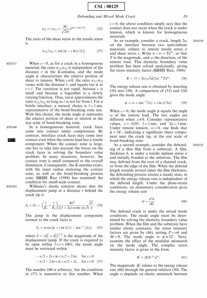
jump. Consequently, the mesh can be coarsenear the crack tip, and the elements need notconform to the crack geometry. As the cracksgrow, one updates the nodes to be enriched.No remeshing is necessary. Figure 16 shows thesimulated mud-crack pattern in tensile filmbonded to a substrate (bib79 Liang et al.,2002b).
8.7.3.2 Interfacial Fracture Mechanics
Now consider a crack on the interfacebetween two elastic materials. Williams (1959)discovered that the singular stress field at theinterface crack tip is not square-root singular.The stresses on the interface a distance r aheadof the crack tip take the form
s22 þ is12 ¼Krieffiffiffiffiffiffiffi2pr
p : ð47Þ
The notation of complex numbers is used: i ¼ffiffiffiffiffiffiffi�1
pand rie ¼ eie ln r ¼ cos ðe ln rÞ þ
i sin ðe ln rÞ: The bimaterial constant e isdefined by
e ¼ 1
2pln
ð3� 4n1Þ=m1 þ 1=m2ð3� 4n2Þ=m2 þ 1=m1
�; ð48Þ
where n is Poisson’s ratio, m the shear modulus,and the subscripts 1 and 2 refer to the two
materials. The constant is bounded, |e|o(1/2p)ln 3E0.175.
The stress intensity factor K is complexvalued, and has the dimension
K ¼ ½stress ½length1=2�ie: ð49Þ
The amplitude of the stress intensity factor hasthe familiar dimension, |K|¼ [stress][length]1/2.Indeed, |K| relates to the energy release rate as
G ¼ 1
2
1
%E1
þ 1
%E2
� �jK j2
cosh2ðpeÞ: ð50Þ
For a given crack configuration, the stressintensity factor K is determined by solving theelasticity boundary value problem. Finite ele-ment method and other numerical methodshave been developed to determine the stressintensity factor (Matos et al., 1990). bib61Hutchinson and Suo (1991) have compiledsolutions for layered materials.
Following bib101 Rice (1988), we define themode angle c by
K ¼ jK jl�ie exp ðicÞ; ð51Þ
where l is an arbitrary length. To see theconsequence of this definition, combine (47)and (51), yielding
Figure 16 Mud-crack pattern simulated by using the XFEM.
SX0320
AU:1
SX0325
AU:2
SX0330
18 Reliability of Interconnect Structures
CSI : 08125
s22 þ i s12 ¼jKjffiffiffiffiffiffiffi2pr
p ei½cþe lnðr=lÞ: ð52Þ
The ratio of the shear stress to the tensile stressis
s12=s22 ¼ tan ½cþ e lnðr=LÞ: ð53Þ
When e¼ 0, as for a crack in a homogenousmaterial, the ratio s12/s22 is independent of thedistance r in the K-annulus, and the modeangle c characterizes the relative portion ofshear to tension. When ea0, the ratio s12/s22varies with the distance r, and equals tan c atr¼ l. The variation is not rapid, because e issmall and because a logarithm is a slowlyvarying function. Thus, tanc approximates theratio s12/s22 so long as r is not far from l. For abrittle interface, a natural choice is l¼ 1 nm,representative of the bond-breaking zone size.With this choice, the mode angle c representsthe relative portion of shear to tension at thesize scale of bond-breaking zone.
In a homogeneous material, crack facescome into contact under compression. Bycontrast, interface crack faces may come intocontact even when the remote load has a tensilecomponent. When the contact zone is large,one has to take into account the forces on thecrack faces in solving the boundary valueproblem. In many situations, however, thecontact zone is small compared to the overalldimension. Consequently, the K-annulus exists,with the inner radius enclosing the contactzone, as well as the bond-breaking processzone. bib101 Rice (1988) has examined thecondition for small-scale contact.
Williams’s elastic solution shows that thedisplacement jump at a distance r behind thecrack tip is
d2 þ id1 ¼1
%E1
þ 1
%E2
� �Krie
2ð1þ 2ieÞ cosh ðpeÞ
ffiffiffiffiffi2r
p
r: ð54Þ
The jump in the displacement componentnormal to the crack faces is
d2 ¼ d cos ½cþ e ln ðl=rÞ � tan�1 ð2eÞ; ð55Þ
where d ¼ ðd21 þ d22Þ1=2 is the magnitude of the
displacement jump. If the crack is required tobe open within loro100 l, the mode anglemust be restricted within
� p=2þ 2eocop=2þ 2:6e; for e40
� p=2� 2:6eocop=2þ 2e; for eo0 ð57Þ
The number 100 is arbitrary, but the conditionin (57) is insensitive to this number. When
e¼ 0, the above condition simply says that thecontact does not occur when the crack is undertension, which is known for homogeneousmaterials.
As an example, consider a crack, length 2a,on the interface between two semi-infinitematerials, subject to remote tensile stress sand shear stress t. Write sþ it¼Teio, so thatT is the magnitude, and o the direction, of theremote load. This elasticity boundary valueproblem has been solved analytically, givingthe stress intensity factor (bib101 Rice, 1988)
K ¼ ð1þ 2ieÞffiffiffiffiffiffipa
pð2aÞ�ie
Teio: ð58Þ
The energy release rate is obtained by inserting(58) into (50). A comparison of (51) and (58)gives the mode angle:
c ¼ oþ tan�1ð2eÞ þ e ln ðl=2aÞ: ð59Þ
When e¼ 0, the mode angle c equals the angleo of the remote load. The two angles aredifferent when ea0. Consider representativevalues, e¼ –0.05, l¼ 1 nm, and 2a¼ 1mm.Under remote tension, o¼ 0, one finds thatc¼ 341, indicating a significant shear compo-nent near the crack tip, at the size scale ofbond-breaking zone.
As a second example, consider the debond-ing of a thin film from a substrate. A film,thickness h, is under a tensile inplane stress sand initially bonded to the substrate. The filmmay debond from the root of a channel crack,or from the edge of the film. When the debondlength exceeds several times the film thickness,the debonding process attains a steady state, inwhich the energy release rate is independent ofthe debond length. Under the plane-strainconditions, an elementary consideration givesthe energy release rate
G ¼ s2h
2 %Ef
: ð60Þ
The debond crack is under the mixed modeconditions. The mode angle must be deter-mined by solving the elasticity boundary valueproblem. When the film and the substrate havesimilar elastic constants, the stress intensityfactors are given by (46), setting P¼ sh andM¼ 0. The mode angle is cE521. Next,examine the effect of the modulus mismatchon the mode angle. The complex stressintensity factor is given in the form
K ¼ jK jh�ie eio: ð61Þ
The magnitude |K| relates to the energy releaserate (60) through the general relation (50). Theangle o depends on elastic mismatch between
SX0331
SX0340
AU:3
SX0345
SX0350
SX0355
Debonding and Mixed Mode Crack 19
CSI : 08125
the film and the substrate, ranging between 401to 601 if the mismatch is not excessive, astabulated in bib120 Suo and Hutchinson(1990). A comparison of (61) and (51) givesthe mode angle
c ¼ oþ e ln ðl=hÞ: ð62Þ
For representative values, e¼ –0.05, l¼ 1 nm,and h¼ 1 mm, the additional angle is e ln (l/h)¼ 201.
8.7.3.3 Measuring Interfacial Fracture Energy
When a debond crack extends on a bimater-ial interface, mixed mode conditions usuallyprevail. The fracture energy is a function of themode angle, G(c). The crack extends when theenergy release rate reaches the fracture energy:G¼G(c). Due to elastic mismatch in the twomaterials, one should specify the length l indefining the mode angle c. The curve G(c) hasbeen measured for a few interface (e.g., bib19Cao and Evans, 1989; bib133 Wang and Suo,1990; bib80 Liechti and Chai, 1991). Figure 17sketches the trend of the G(c) curve. Thefracture energy tends to increase as mode angleapproaches 7p/2. The energy cost for debondvaries with the relative proportion of openingand shearing modes, because, e.g., a largeamount of shear may promote more inelasticdeformation in the constituent materials, orpromote near-tip sliding against roughness ifthe interface is not perfectly flat. The curveG(c) need not be symmetric with respect toc¼ 0, because the two materials on either sideof the interface are dissimilar, breaking thesymmetry between co0 and c40.
Many test configurations for measuringinterfacial fracture energy exist. (See reviewsby bib61 Hutchinson and Suo (1991), bib31Evans and Hutchinson (1995), and bib132Volinsky et al. (2002).) For example, theprocess of a tensile film debonding from asubstrate is a means to determine the inter-facial fracture energy. To ensure that the crackis in the steady state, one should introduce aninitial debond crack of length several times thefilm thickness (bib139 Yu et al., 2001). Theenergy release rate (60) depends on both thefilm stress and the film thickness. One maychange the film stress by varying the tempera-ture, or by applying a mechanical load such aspulling the substrate. One may change the filmthickness during deposition. The combinationof the stress and the thickness that cause thedebond crack to grow gives the fracture energyaccording to (60). It is often more convenientto deposit a layer of a different material toincrease the energy release rate. For example,
Cr has been used as an overlayer for its highresidual stress (bib8 Bagchi et al., 1994). Thickepoxy overlayers have also been used (bib108Shaffer et al., 1996). When an overlayer is used,one should obtain a different energy releaserate expression, and introduce an initialdebond crack of length several times of thecombined thickness of the film and the over-layer.
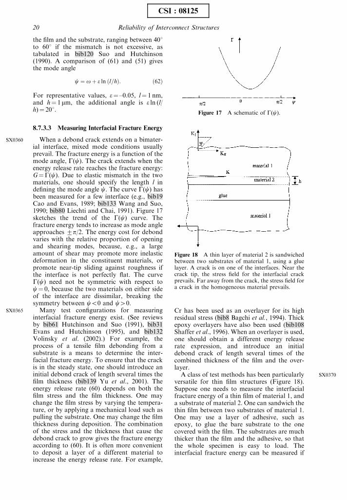
A class of test methods has been particularlyversatile for thin film structures (Figure 18).Suppose one needs to measure the interfacialfracture energy of a thin film of material 1, anda substrate of material 2. One can sandwich thethin film between two substrates of material 1.One may use a layer of adhesive, such asepoxy, to glue the bare substrate to the onecovered with the film. The substrates are muchthicker than the film and the adhesive, so thatthe whole specimen is easy to load. Theinterfacial fracture energy can be measured if
Figure 18 A thin layer of material 2 is sandwichedbetween two substrates of material 1, using a gluelayer. A crack is on one of the interfaces. Near thecrack tip, the stress field for the interfacial crackprevails. Far away from the crack, the stress field fora crack in the homogeneous material prevails.
Figure 17 A schematic of G(c).
SX0360
SX0365
SX0370
20 Reliability of Interconnect Structures
CSI : 08125
the crack runs on the desired interface. Thereare several advantages of methods of this kind.First, the methods are applicable for thin filmsof any thickness, and can even measure theinterfacial energy between two thin films, whenthey are both sandwiched. Second, because thefilm is still bonded to one substrate in the crackwake, the residual stress in the film isunrelieved, and therefore does not contributeto the energy release rate. Third, the experi-mental data are relatively easy to interpret, asexplained below.
Let us return to Figure 18. Because thesubstrates are much thicker than the films, thestress field in the substrate, far away from thefilms, is unaffected by the presence of the films,and is the same as that around a crack in ahomogeneous body, given in the form (39). Theload on the substrate can be represented by thetwo stress intensity factors KI and KII for acrack in a homogenous body. Near the cracktip, the stress field is that of an interfacial crack(47), characterized by the complex stressintensity factor K. The energy release rate isrelated to both the far field and the near-tipfield, namely,
G ¼ 1
%E1
ðK2I þ K2
IIÞ ¼1
2
1
%E1
þ 1
%E2
� �jK j2
cosh2ðpeÞ: ð63Þ
The energy release rate can be calculated fromthe homogeneous specimen, neglecting the thinfilms.
The mode angle, however, has to be deter-mined by solving the boundary value problemthat includes the thin films. Let cN be themode angle of the remote load, namely,tancN¼KII/KI. The local mode angle c isdefined by (51) using an arbitrary length l. Thelocal mode angle relates to the remote modeangle as
c ¼ cN
þ oþ e ln ðl=hÞ; ð64Þ
where h is the thickness of one of the films, ando is an angle that depends on the elasticproperties of the films and the substrates, aswell as the ratios between various films. bib119Suo and Hutchinson (1989) solved the case of asingle film between two substrates, and foundthat o is less than 101 provided the elasticmismatch is not too large. It is rather cumber-some to keep track of the local mode angle,especially when several films are sandwiched,and when some of them deform plastically. Acommon practice has been to specify the modeangle for the sandwich specimens by theremote value cN.
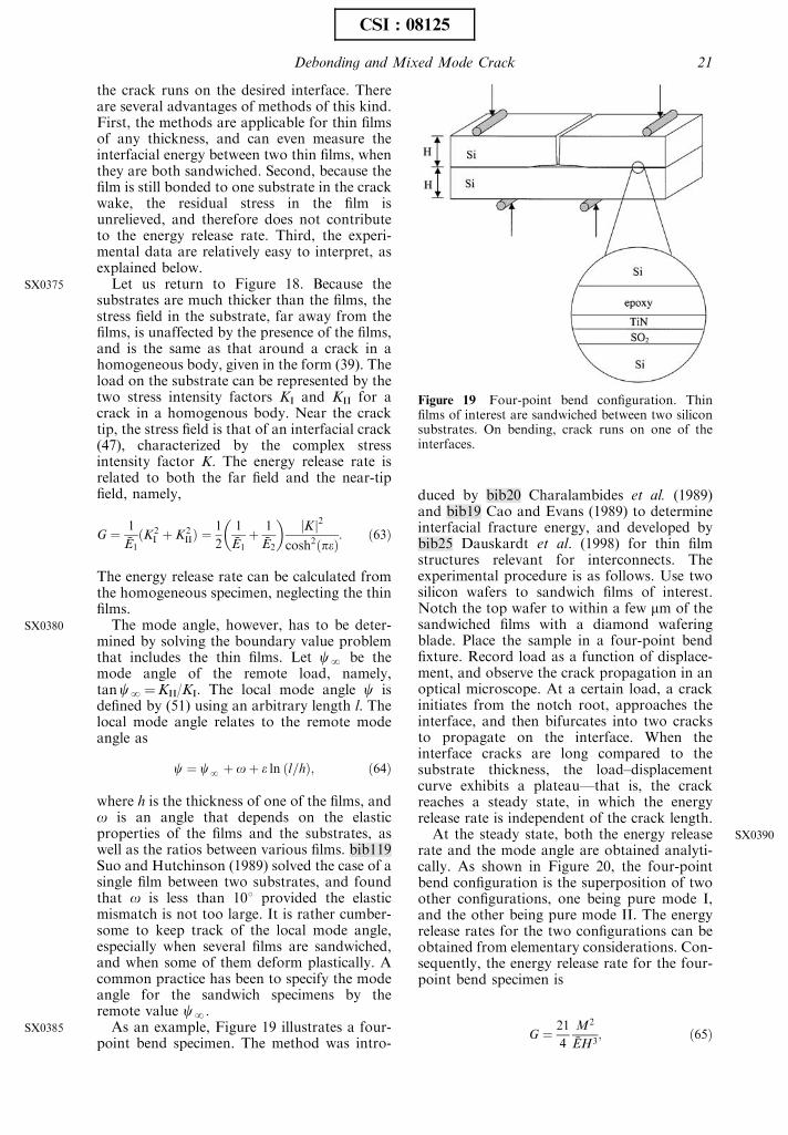
As an example, Figure 19 illustrates a four-point bend specimen. The method was intro-
duced by bib20 Charalambides et al. (1989)and bib19 Cao and Evans (1989) to determineinterfacial fracture energy, and developed bybib25 Dauskardt et al. (1998) for thin filmstructures relevant for interconnects. Theexperimental procedure is as follows. Use twosilicon wafers to sandwich films of interest.Notch the top wafer to within a few mm of thesandwiched films with a diamond waferingblade. Place the sample in a four-point bendfixture. Record load as a function of displace-ment, and observe the crack propagation in anoptical microscope. At a certain load, a crackinitiates from the notch root, approaches theinterface, and then bifurcates into two cracksto propagate on the interface. When theinterface cracks are long compared to thesubstrate thickness, the load–displacementcurve exhibits a plateau—that is, the crackreaches a steady state, in which the energyrelease rate is independent of the crack length.
At the steady state, both the energy releaserate and the mode angle are obtained analyti-cally. As shown in Figure 20, the four-pointbend configuration is the superposition of twoother configurations, one being pure mode I,and the other being pure mode II. The energyrelease rates for the two configurations can beobtained from elementary considerations. Con-sequently, the energy release rate for the four-point bend specimen is
G ¼ 21
4
M2
%EH3; ð65Þ
Figure 19 Four-point bend configuration. Thinfilms of interest are sandwiched between two siliconsubstrates. On bending, crack runs on one of theinterfaces.
SX0375
SX0380
SX0385
SX0390
Debonding and Mixed Mode Crack 21
CSI : 08125
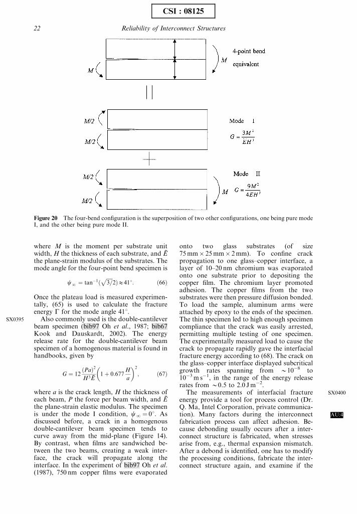
where M is the moment per substrate unitwidth, H the thickness of each substrate, and %Ethe plane-strain modulus of the substrates. Themode angle for the four-point bend specimen is
cN
¼ tan�1ðffiffiffiffiffi3=
p2ÞE411: ð66Þ
Once the plateau load is measured experimen-tally, (65) is used to calculate the fractureenergy G for the mode angle 411.
Also commonly used is the double-cantileverbeam specimen (bib97 Oh et al., 1987; bib67Kook and Dauskardt, 2002). The energyrelease rate for the double-cantilever beamspecimen of a homogenous material is found inhandbooks, given by
G ¼ 12ðPaÞ2
H3 %E1þ 0:677
H
a
� �2
; ð67Þ
where a is the crack length, H the thickness ofeach beam, P the force per beam width, and %Ethe plane-strain elastic modulus. The specimenis under the mode I condition, cN¼ 01. Asdiscussed before, a crack in a homogenousdouble-cantilever beam specimen tends tocurve away from the mid-plane (Figure 14).By contrast, when films are sandwiched be-tween the two beams, creating a weak inter-face, the crack will propagate along theinterface. In the experiment of bib97 Oh et al.(1987), 750 nm copper films were evaporated
onto two glass substrates (of size75mm� 25mm� 2mm). To confine crackpropagation to one glass–copper interface, alayer of 10–20 nm chromium was evaporatedonto one substrate prior to depositing thecopper film. The chromium layer promotedadhesion. The copper films from the twosubstrates were then pressure diffusion bonded.To load the sample, aluminum arms wereattached by epoxy to the ends of the specimen.The thin specimen led to high enough specimencompliance that the crack was easily arrested,permitting multiple testing of one specimen.The experimentally measured load to cause thecrack to propagate rapidly gave the interfacialfracture energy according to (68). The crack onthe glass–copper interface displayed subcriticalgrowth rates spanning from B10�8 to10�3m s�1, in the range of the energy releaserates from B0.5 to 2.0 Jm�2.
The measurements of interfacial fractureenergy provide a tool for process control (Dr.Q. Ma, Intel Corporation, private communica-tion). Many factors during the interconnectfabrication process can affect adhesion. Be-cause debonding usually occurs after a inter-connect structure is fabricated, when stressesarise from, e.g., thermal expansion mismatch.After a debond is identified, one has to modifythe processing conditions, fabricate the inter-connect structure again, and examine if the
Figure 20 The four-bend configuration is the superposition of two other configurations, one being pure modeI, and the other being pure mode II.
SX0395
SX0400
AU:4
22 Reliability of Interconnect Structures
CSI : 08125
new structure has the debond. The iteration istime consuming. Alternatively, without fabri-cating the whole interconnect structure, onecan measure the interfacial fracture energy forthe interface at question under various fabrica-tion conditions, and then select the conditionthat gives an adequate interfacial fractureenergy.
The measurements of interfacial fractureenergy also provide a tool to select materialsto promote adhesion. When copper wasintroduced into the interconnect structure inlate 1990s, new barrier layers were required toprevent copper diffusion into dielectrics, and toprovide adhesion of copper to the dielectrics.The sandwiched four-point bend specimenswere used to measure the interfacial fractureenergy of the thin film structures with Ta andTaN as barrier layers (bib72 Lane et al., 2000),and thereby to study the effects of interfacialchemistry, copper layer thickness, and dielec-tric type on adhesion. Subsequently, numerousmaterials of low dielectric constant have beendeveloped to compete to be a replacement forsilica in the interconnect structure. To comparethese materials, a commonly accepted methodis desired to measure the interfacial fractureenergy. bib102 Rim et al. (2002) have evaluatedadhesion of a carbon-doped oxide in thin filmstructures.
Interfacial cracks are often susceptible tosubcritical growth under static or cyclic load.Environment strongly affects the growth rate.While the implications of subcritical debondgrowth for long-term reliability of the inter-connect structure have not been fully under-stood, the fracture specimens discussed abovehave been used to study subcritical debondgrowth (bib67 Kook and Dauskardt, 2002;bib112 Snodgrass et al., 2002).
8.7.3.4 Effects of Plasticity
The above discussions are confined in thelinear elastic fracture mechanics (LEFM). Oneof the main requirements of the LEFM is thatthe inelastic zone around the crack tip must bemuch smaller than the feature size, in our case,the film thickness. The inelastic deformationwithin the small zone is accounted for by thefracture energy. In computing the energyrelease rate, the structure is taken to be elastic.When the inelastic zone is large compared tothe film thickness, however, we must considerthe inelastic deformation more explicitly. Thefollowing examples illustrate roles played byplasticity.
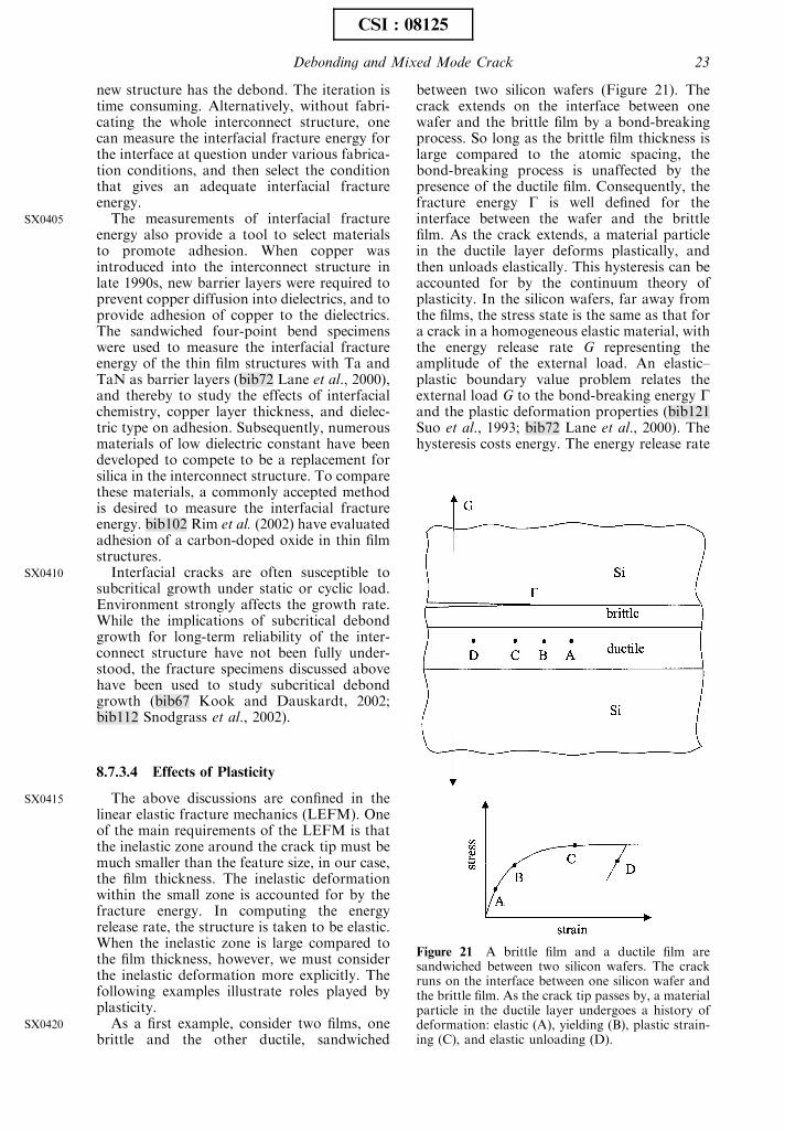
As a first example, consider two films, onebrittle and the other ductile, sandwiched
between two silicon wafers (Figure 21). Thecrack extends on the interface between onewafer and the brittle film by a bond-breakingprocess. So long as the brittle film thickness islarge compared to the atomic spacing, thebond-breaking process is unaffected by thepresence of the ductile film. Consequently, thefracture energy G is well defined for theinterface between the wafer and the brittlefilm. As the crack extends, a material particlein the ductile layer deforms plastically, andthen unloads elastically. This hysteresis can beaccounted for by the continuum theory ofplasticity. In the silicon wafers, far away fromthe films, the stress state is the same as that fora crack in a homogeneous elastic material, withthe energy release rate G representing theamplitude of the external load. An elastic–plastic boundary value problem relates theexternal load G to the bond-breaking energy Gand the plastic deformation properties (bib121Suo et al., 1993; bib72 Lane et al., 2000). Thehysteresis costs energy. The energy release rate
Figure 21 A brittle film and a ductile film aresandwiched between two silicon wafers. The crackruns on the interface between one silicon wafer andthe brittle film. As the crack tip passes by, a materialparticle in the ductile layer undergoes a history ofdeformation: elastic (A), yielding (B), plastic strain-ing (C), and elastic unloading (D).
SX0405
SX0410
SX0415
SX0420
Debonding and Mixed Mode Crack 23
CSI : 08125
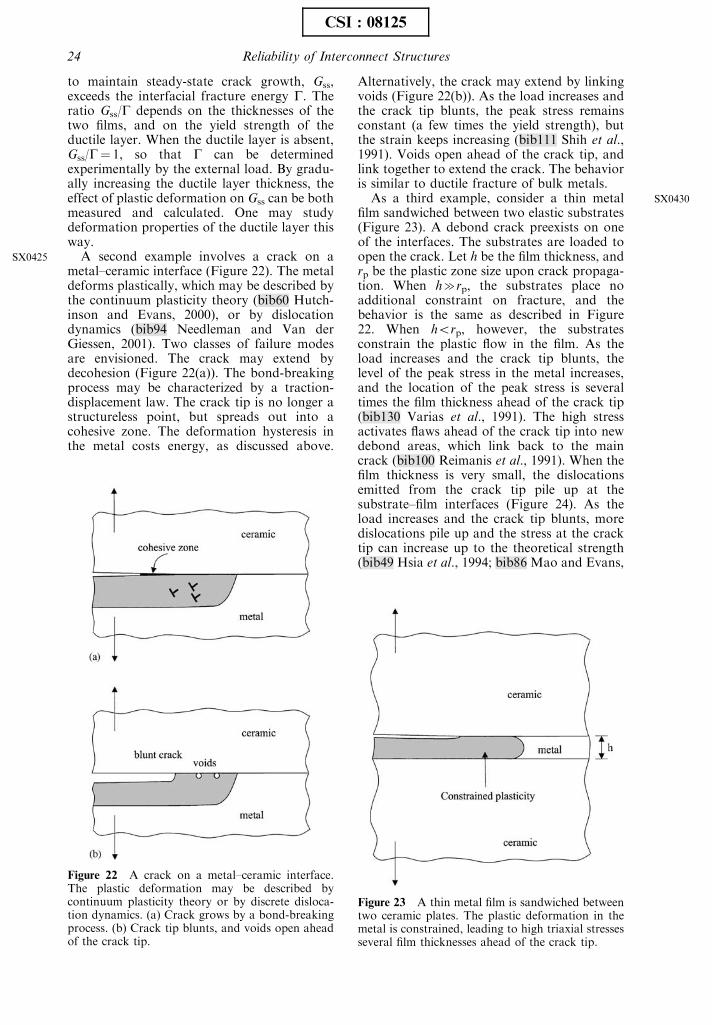
to maintain steady-state crack growth, Gss,exceeds the interfacial fracture energy G. Theratio Gss/G depends on the thicknesses of thetwo films, and on the yield strength of theductile layer. When the ductile layer is absent,Gss/G¼ 1, so that G can be determinedexperimentally by the external load. By gradu-ally increasing the ductile layer thickness, theeffect of plastic deformation on Gss can be bothmeasured and calculated. One may studydeformation properties of the ductile layer thisway.
A second example involves a crack on ametal–ceramic interface (Figure 22). The metaldeforms plastically, which may be described bythe continuum plasticity theory (bib60 Hutch-inson and Evans, 2000), or by dislocationdynamics (bib94 Needleman and Van derGiessen, 2001). Two classes of failure modesare envisioned. The crack may extend bydecohesion (Figure 22(a)). The bond-breakingprocess may be characterized by a traction-displacement law. The crack tip is no longer astructureless point, but spreads out into acohesive zone. The deformation hysteresis inthe metal costs energy, as discussed above.
Alternatively, the crack may extend by linkingvoids (Figure 22(b)). As the load increases andthe crack tip blunts, the peak stress remainsconstant (a few times the yield strength), butthe strain keeps increasing (bib111 Shih et al.,1991). Voids open ahead of the crack tip, andlink together to extend the crack. The behavioris similar to ductile fracture of bulk metals.
As a third example, consider a thin metalfilm sandwiched between two elastic substrates(Figure 23). A debond crack preexists on oneof the interfaces. The substrates are loaded toopen the crack. Let h be the film thickness, andrp be the plastic zone size upon crack propaga-tion. When hcrp, the substrates place noadditional constraint on fracture, and thebehavior is the same as described in Figure22. When horp, however, the substratesconstrain the plastic flow in the film. As theload increases and the crack tip blunts, thelevel of the peak stress in the metal increases,and the location of the peak stress is severaltimes the film thickness ahead of the crack tip(bib130 Varias et al., 1991). The high stressactivates flaws ahead of the crack tip into newdebond areas, which link back to the maincrack (bib100 Reimanis et al., 1991). When thefilm thickness is very small, the dislocationsemitted from the crack tip pile up at thesubstrate–film interfaces (Figure 24). As theload increases and the crack tip blunts, moredislocations pile up and the stress at the cracktip can increase up to the theoretical strength(bib49 Hsia et al., 1994; bib86 Mao and Evans,
Figure 23 A thin metal film is sandwiched betweentwo ceramic plates. The plastic deformation in themetal is constrained, leading to high triaxial stressesseveral film thicknesses ahead of the crack tip.
Figure 22 A crack on a metal–ceramic interface.The plastic deformation may be described bycontinuum plasticity theory or by discrete disloca-tion dynamics. (a) Crack grows by a bond-breakingprocess. (b) Crack tip blunts, and voids open aheadof the crack tip.
SX0425
SX0430
24 Reliability of Interconnect Structures
CSI : 08125
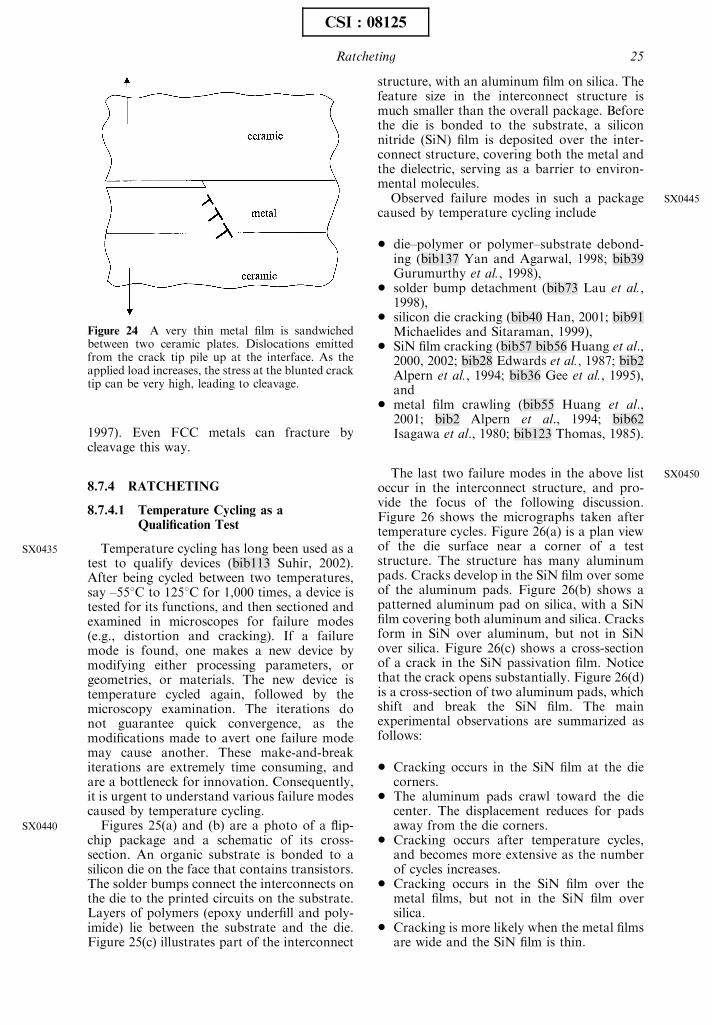
1997). Even FCC metals can fracture bycleavage this way.
8.7.4 RATCHETING
8.7.4.1 Temperature Cycling as aQualification Test
Temperature cycling has long been used as atest to qualify devices (bib113 Suhir, 2002).After being cycled between two temperatures,say –551C to 1251C for 1,000 times, a device istested for its functions, and then sectioned andexamined in microscopes for failure modes(e.g., distortion and cracking). If a failuremode is found, one makes a new device bymodifying either processing parameters, orgeometries, or materials. The new device istemperature cycled again, followed by themicroscopy examination. The iterations donot guarantee quick convergence, as themodifications made to avert one failure modemay cause another. These make-and-breakiterations are extremely time consuming, andare a bottleneck for innovation. Consequently,it is urgent to understand various failure modescaused by temperature cycling.
Figures 25(a) and (b) are a photo of a flip-chip package and a schematic of its cross-section. An organic substrate is bonded to asilicon die on the face that contains transistors.The solder bumps connect the interconnects onthe die to the printed circuits on the substrate.Layers of polymers (epoxy underfill and poly-imide) lie between the substrate and the die.Figure 25(c) illustrates part of the interconnect
structure, with an aluminum film on silica. Thefeature size in the interconnect structure ismuch smaller than the overall package. Beforethe die is bonded to the substrate, a siliconnitride (SiN) film is deposited over the inter-connect structure, covering both the metal andthe dielectric, serving as a barrier to environ-mental molecules.
Observed failure modes in such a packagecaused by temperature cycling include
* die–polymer or polymer–substrate debond-ing (bib137 Yan and Agarwal, 1998; bib39Gurumurthy et al., 1998),
* solder bump detachment (bib73 Lau et al.,1998),
* silicon die cracking (bib40 Han, 2001; bib91Michaelides and Sitaraman, 1999),
* SiN film cracking (bib57 bib56 Huang et al.,2000, 2002; bib28 Edwards et al., 1987; bib2Alpern et al., 1994; bib36 Gee et al., 1995),and
* metal film crawling (bib55 Huang et al.,2001; bib2 Alpern et al., 1994; bib62Isagawa et al., 1980; bib123 Thomas, 1985).
The last two failure modes in the above listoccur in the interconnect structure, and pro-vide the focus of the following discussion.Figure 26 shows the micrographs taken aftertemperature cycles. Figure 26(a) is a plan viewof the die surface near a corner of a teststructure. The structure has many aluminumpads. Cracks develop in the SiN film over someof the aluminum pads. Figure 26(b) shows apatterned aluminum pad on silica, with a SiNfilm covering both aluminum and silica. Cracksform in SiN over aluminum, but not in SiNover silica. Figure 26(c) shows a cross-sectionof a crack in the SiN passivation film. Noticethat the crack opens substantially. Figure 26(d)is a cross-section of two aluminum pads, whichshift and break the SiN film. The mainexperimental observations are summarized asfollows:
* Cracking occurs in the SiN film at the diecorners.
* The aluminum pads crawl toward the diecenter. The displacement reduces for padsaway from the die corners.
* Cracking occurs after temperature cycles,and becomes more extensive as the numberof cycles increases.
* Cracking occurs in the SiN film over themetal films, but not in the SiN film oversilica.
* Cracking is more likely when the metal filmsare wide and the SiN film is thin.
Figure 24 A very thin metal film is sandwichedbetween two ceramic plates. Dislocations emittedfrom the crack tip pile up at the interface. As theapplied load increases, the stress at the blunted cracktip can be very high, leading to cleavage.
SX0435
SX0440
SX0445
SX0450
Ratcheting 25
CSI : 08125
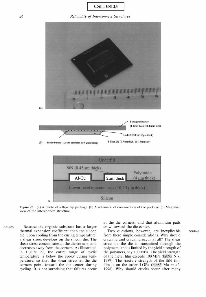
Because the organic substrate has a largerthermal expansion coefficient than the silicondie, upon cooling from the curing temperature,a shear stress develops on the silicon die. Theshear stress concentrates at the die corners, anddecreases away from the corners. As illustratedin Figure 27, the entire range of cyclictemperature is below the epoxy curing tem-perature, so that the shear stress at the diecorners point toward the die center duringcycling. It is not surprising that failures occur
at the die corners, and that aluminum padscrawl toward the die center.
Two questions, however, are inexplicablefrom these simple considerations. Why shouldcrawling and cracking occur at all? The shearstress on the die is transmitted through thepolymers, and is limited by the yield strength ofthe polymers, say 100MPa. The yield strengthof the metal film exceeds 100MPa (bib95 Nix,1989). The fracture strength of the SiN thinfilm is on the order 1GPa (bib85 Ma et al.,1998). Why should cracks occur after many
Figure 25 (a) A photo of a flip-chip package. (b) A schematic of cross-section of the package. (c) Magnifiedview of the interconnect structure.
SX0455
SX0460
26 Reliability of Interconnect Structures
CSI : 08125
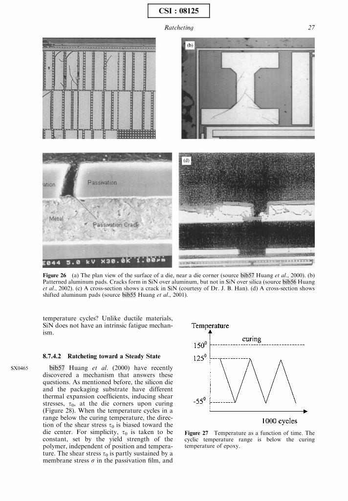
temperature cycles? Unlike ductile materials,SiN does not have an intrinsic fatigue mechan-ism.
8.7.4.2 Ratcheting toward a Steady State
bib57 Huang et al. (2000) have recentlydiscovered a mechanism that answers thesequestions. As mentioned before, the silicon dieand the packaging substrate have differentthermal expansion coefficients, inducing shearstresses, t0, at the die corners upon curing(Figure 28). When the temperature cycles in arange below the curing temperature, the direc-tion of the shear stress t0 is biased toward thedie center. For simplicity, t0 is taken to beconstant, set by the yield strength of thepolymer, independent of position and tempera-ture. The shear stress t0 is partly sustained by amembrane stress s in the passivation film, and
Figure 26 (a) The plan view of the surface of a die, near a die corner (source bib57 Huang et al., 2000). (b)Patterned aluminum pads. Cracks form in SiN over aluminum, but not in SiN over silica (source bib56 Huanget al., 2002). (c) A cross-section shows a crack in SiN (courtesy of Dr. J. B. Han). (d) A cross-section showsshifted aluminum pads (source bib55 Huang et al., 2001).
Figure 27 Temperature as a function of time. Thecyclic temperature range is below the curingtemperature of epoxy.
SX0465
Ratcheting 27
CSI : 08125
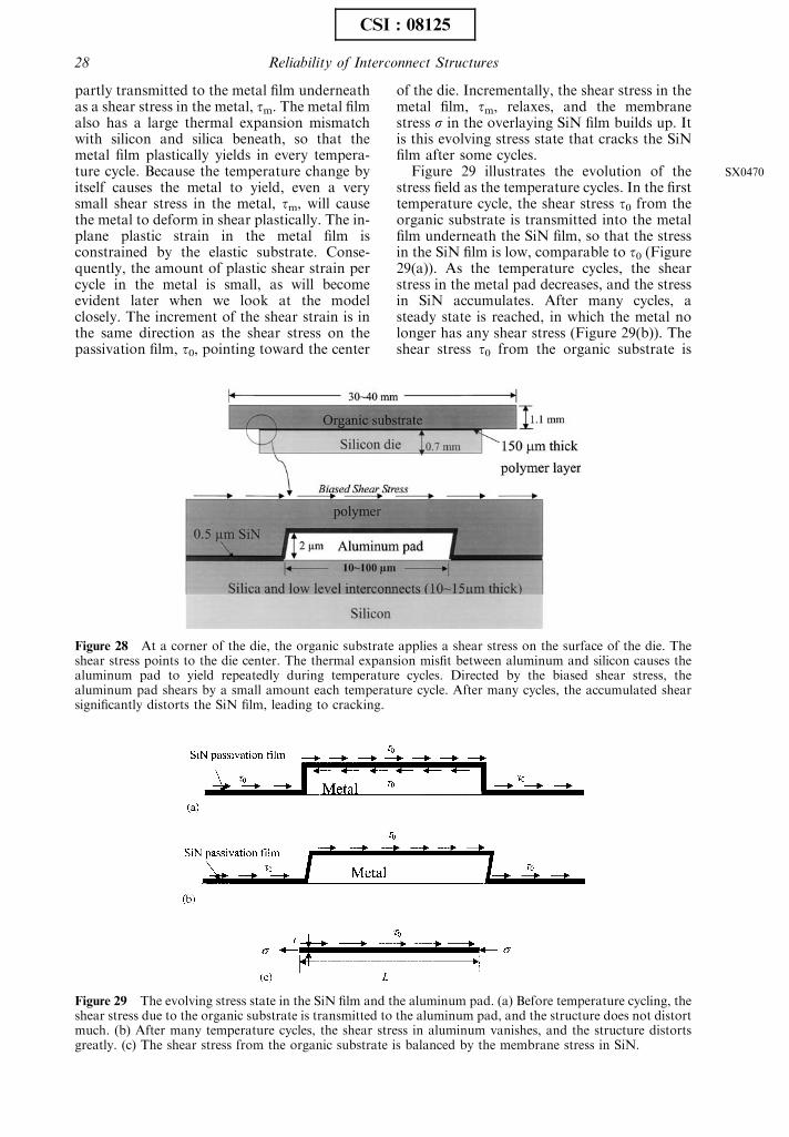
partly transmitted to the metal film underneathas a shear stress in the metal, tm. The metal filmalso has a large thermal expansion mismatchwith silicon and silica beneath, so that themetal film plastically yields in every tempera-ture cycle. Because the temperature change byitself causes the metal to yield, even a verysmall shear stress in the metal, tm, will causethe metal to deform in shear plastically. The in-plane plastic strain in the metal film isconstrained by the elastic substrate. Conse-quently, the amount of plastic shear strain percycle in the metal is small, as will becomeevident later when we look at the modelclosely. The increment of the shear strain is inthe same direction as the shear stress on thepassivation film, t0, pointing toward the center
of the die. Incrementally, the shear stress in themetal film, tm, relaxes, and the membranestress s in the overlaying SiN film builds up. Itis this evolving stress state that cracks the SiNfilm after some cycles.
Figure 29 illustrates the evolution of thestress field as the temperature cycles. In the firsttemperature cycle, the shear stress t0 from theorganic substrate is transmitted into the metalfilm underneath the SiN film, so that the stressin the SiN film is low, comparable to t0 (Figure29(a)). As the temperature cycles, the shearstress in the metal pad decreases, and the stressin SiN accumulates. After many cycles, asteady state is reached, in which the metal nolonger has any shear stress (Figure 29(b)). Theshear stress t0 from the organic substrate is
Figure 28 At a corner of the die, the organic substrate applies a shear stress on the surface of the die. Theshear stress points to the die center. The thermal expansion misfit between aluminum and silicon causes thealuminum pad to yield repeatedly during temperature cycles. Directed by the biased shear stress, thealuminum pad shears by a small amount each temperature cycle. After many cycles, the accumulated shearsignificantly distorts the SiN film, leading to cracking.
Figure 29 The evolving stress state in the SiN film and the aluminum pad. (a) Before temperature cycling, theshear stress due to the organic substrate is transmitted to the aluminum pad, and the structure does not distortmuch. (b) After many temperature cycles, the shear stress in aluminum vanishes, and the structure distortsgreatly. (c) The shear stress from the organic substrate is balanced by the membrane stress in SiN.
SX0470
28 Reliability of Interconnect Structures
CSI : 08125
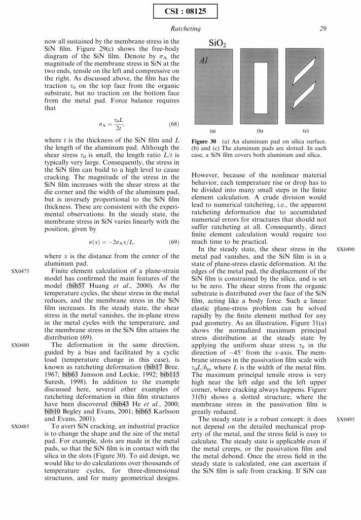
now all sustained by the membrane stress in theSiN film. Figure 29(c) shows the free-bodydiagram of the SiN film. Denote by sA themagnitude of the membrane stress in SiN at thetwo ends, tensile on the left and compressive onthe right. As discussed above, the film has thetraction t0 on the top face from the organicsubstrate, but no traction on the bottom facefrom the metal pad. Force balance requiresthat
sA ¼ t0L
2t; ð68Þ
where t is the thickness of the SiN film and Lthe length of the aluminum pad. Although theshear stress t0 is small, the length ratio L/t istypically very large. Consequently, the stress inthe SiN film can build to a high level to causecracking. The magnitude of the stress in theSiN film increases with the shear stress at thedie corner and the width of the aluminum pad,but is inversely proportional to the SiN filmthickness. These are consistent with the experi-mental observations. In the steady state, themembrane stress in SiN varies linearly with theposition, given by
sðxÞ ¼ �2sAx=L; ð69Þ
where x is the distance from the center of thealuminum pad.
Finite element calculation of a plane-strainmodel has confirmed the main features of themodel (bib57 Huang et al., 2000). As thetemperature cycles, the shear stress in the metalreduces, and the membrane stress in the SiNfilm increases. In the steady state, the shearstress in the metal vanishes, the in-plane stressin the metal cycles with the temperature, andthe membrane stress in the SiN film attains thedistribution (69).
The deformation in the same direction,guided by a bias and facilitated by a cyclicload (temperature change in this case), isknown as ratcheting deformation (bib17 Bree,1967; bib63 Jansson and Leckie, 1992; bib115Suresh, 1998). In addition to the examplediscussed here, several other examples ofratcheting deformation in thin film structureshave been discovered (bib43 He et al., 2000;bib10 Begley and Evans, 2001; bib65 Karlssonand Evans, 2001).
To avert SiN cracking, an industrial practiceis to change the shape and the size of the metalpad. For example, slots are made in the metalpads, so that the SiN film is in contact with thesilica in the slots (Figure 30). To aid design, wewould like to do calculations over thousands oftemperature cycles, for three-dimensionalstructures, and for many geometrical designs.
However, because of the nonlinear materialbehavior, each temperature rise or drop has tobe divided into many small steps in the finiteelement calculation. A crude division wouldlead to numerical ratcheting, i.e., the apparentratcheting deformation due to accumulatednumerical errors for structures that should notsuffer ratcheting at all. Consequently, directfinite element calculation would require toomuch time to be practical.
In the steady state, the shear stress in themetal pad vanishes, and the SiN film is in astate of plane-stress elastic deformation. At theedges of the metal pad, the displacement of theSiN film is constrained by the silica, and is setto be zero. The shear stress from the organicsubstrate is distributed over the face of the SiNfilm, acting like a body force. Such a linearelastic plane-stress problem can be solvedrapidly by the finite element method for anypad geometry. As an illustration, Figure 31(a)shows the normalized maximum principalstress distribution at the steady state byapplying the uniform shear stress t0 in thedirection of �451 from the x-axis. The mem-brane stresses in the passivation film scale witht0L/hp, where L is the width of the metal film.The maximum principal tensile stress is veryhigh near the left edge and the left uppercorner, where cracking always happens. Figure31(b) shows a slotted structure, where themembrane stress in the passivation film isgreatly reduced.
The steady state is a robust concept: it doesnot depend on the detailed mechanical prop-erty of the metal, and the stress field is easy tocalculate. The steady state is applicable even ifthe metal creeps, or the passivation film andthe metal debond. Once the stress field in thesteady state is calculated, one can ascertain ifthe SiN film is safe from cracking. If SiN can
Figure 30 (a) An aluminum pad on silica surface.(b) and (c) The aluminum pads are slotted. In eachcase, a SiN film covers both aluminum and silica.
SX0475
SX0480
SX0485
SX0490
SX0495
Ratcheting 29
CSI : 08125
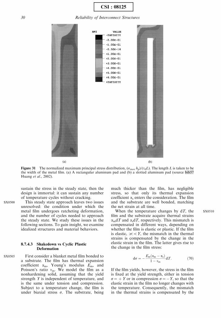
sustain the stress in the steady state, then thedesign is immortal: it can sustain any numberof temperature cycles without cracking.
This steady state approach leaves two issuesunresolved: the condition under which themetal film undergoes ratcheting deformation,and the number of cycles needed to approachthe steady state. We study these issues in thefollowing sections. To gain insight, we examineidealized structures and material behaviors.
8.7.4.3 Shakedown vs Cyclic PlasticDeformation
First consider a blanket metal film bonded toa substrate. The film has thermal expansioncoefficient am, Young’s modulus Em, andPoisson’s ratio nm. We model the film as anonhardening solid, assuming that the yieldstrength Y is independent of temperature, andis the same under tension and compression.Subject to a temperature change, the film isunder biaxial stress s. The substrate, being
much thicker than the film, has negligiblestress, so that only its thermal expansioncoefficient as enters the consideration. The filmand the substrate are well bonded, matchingthe net strain at all time.
When the temperature changes by dT, thefilm and the substrate acquire thermal strainsamdT and asdT, respectively. This mismatch iscompensated in different ways, depending onwhether the film is elastic or plastic. If the filmis elastic, |s|oY, the mismatch in the thermalstrains is compensated by the change in theelastic strain in the film. The latter gives rise tothe change in the film stress:
ds ¼ � Emðam � asÞ1� nm
dT : ð70Þ
If the film yields, however, the stress in the filmis fixed at the yield strength, either in tensions¼ þY or in compression s¼�Y, so that theelastic strain in the film no longer changes withthe temperature. Consequently, the mismatchin the thermal strains is compensated by the
Figure 31 The normalized maximum principal stress distribution, (smax hp)/(t0L). The length L is taken to bethe width of the metal film. (a) A rectangular aluminum pad and (b) a slotted aluminum pad (source bib57Huang et al., 2002).
SX0500
SX0505
SX0510
30 Reliability of Interconnect Structures
CSI : 08125
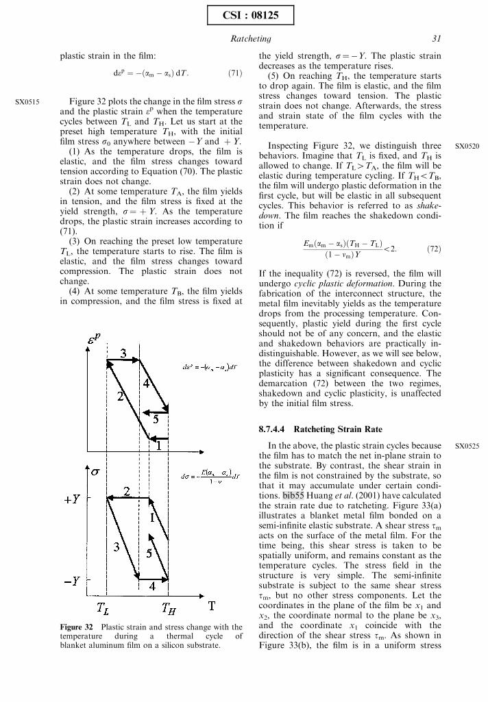
plastic strain in the film:
dep ¼ �ðam � asÞ dT : ð71Þ
Figure 32 plots the change in the film stress sand the plastic strain ep when the temperaturecycles between TL and TH. Let us start at thepreset high temperature TH, with the initialfilm stress s0 anywhere between �Y and þY.
(1) As the temperature drops, the film iselastic, and the film stress changes towardtension according to Equation (70). The plasticstrain does not change.
(2) At some temperature TA, the film yieldsin tension, and the film stress is fixed at theyield strength, s¼ þY. As the temperaturedrops, the plastic strain increases according to(71).
(3) On reaching the preset low temperatureTL, the temperature starts to rise. The film iselastic, and the film stress changes towardcompression. The plastic strain does notchange.
(4) At some temperature TB, the film yieldsin compression, and the film stress is fixed at
the yield strength, s¼�Y. The plastic straindecreases as the temperature rises.
(5) On reaching TH, the temperature startsto drop again. The film is elastic, and the filmstress changes toward tension. The plasticstrain does not change. Afterwards, the stressand strain state of the film cycles with thetemperature.
Inspecting Figure 32, we distinguish threebehaviors. Imagine that TL is fixed, and TH isallowed to change. If TL4TA, the film will beelastic during temperature cycling. If THoTB,the film will undergo plastic deformation in thefirst cycle, but will be elastic in all subsequentcycles. This behavior is referred to as shake-down. The film reaches the shakedown condi-tion if
Emðam � asÞðTH � TLÞð1� nmÞY
o2: ð72Þ
If the inequality (72) is reversed, the film willundergo cyclic plastic deformation. During thefabrication of the interconnect structure, themetal film inevitably yields as the temperaturedrops from the processing temperature. Con-sequently, plastic yield during the first cycleshould not be of any concern, and the elasticand shakedown behaviors are practically in-distinguishable. However, as we will see below,the difference between shakedown and cyclicplasticity has a significant consequence. Thedemarcation (72) between the two regimes,shakedown and cyclic plasticity, is unaffectedby the initial film stress.
8.7.4.4 Ratcheting Strain Rate
In the above, the plastic strain cycles becausethe film has to match the net in-plane strain tothe substrate. By contrast, the shear strain inthe film is not constrained by the substrate, sothat it may accumulate under certain condi-tions. bib55 Huang et al. (2001) have calculatedthe strain rate due to ratcheting. Figure 33(a)illustrates a blanket metal film bonded on asemi-infinite elastic substrate. A shear stress tmacts on the surface of the metal film. For thetime being, this shear stress is taken to bespatially uniform, and remains constant as thetemperature cycles. The stress field in thestructure is very simple. The semi-infinitesubstrate is subject to the same shear stresstm, but no other stress components. Let thecoordinates in the plane of the film be x1 andx2, the coordinate normal to the plane be x3,and the coordinate x1 coincide with thedirection of the shear stress tm. As shown inFigure 33(b), the film is in a uniform stress
Figure 32 Plastic strain and stress change with thetemperature during a thermal cycle ofblanket aluminum film on a silicon substrate.
SX0515
SX0520
SX0525
Ratcheting 31
CSI : 08125

state of a combination of a biaxial stress and ashear stress:
s11 ¼ s22 ¼ sm; s13 ¼ tm; s23 ¼ s12 ¼ 0: ð73Þ
The biaxial stress sm changes with the tem-perature. Obviously, the uniform stress statesin the substrate and in the film satisfy theequilibrium conditions.
To model plastic deformation in the metalfilm, we adopt the J2 flow theory (bib44 Hill,1950). The deviatoric stress tensor, sij ¼ sij �skkdij=3; has the components
s11 ¼ s22 ¼ sm=3; s33 ¼ �2sm=3; s13 ¼ tm;
s23 ¼ s12 ¼ 0: ð74Þ
The Mises yield condition, 3sij sij=2 ¼ Y 2; is
specialized to
s2m þ 3t2m ¼ Y 2: ð75Þ
The yield condition is an ellipse on the sm–tmplane (Figure 33(c)). The metal film is elasticwhen the stress state is inside the ellipse, andyields when the stress state is on the ellipse. Thestress state outside the ellipse is unreachable.When the film yields, for a given tm, the biaxialstress can only be at one of the two levels:
sm ¼ 7ffiffiffiffiffiffiffiffiffiffiffiffiffiffiffiffiffiffiffiffiY 2 � 3t2m
q: ð76Þ
These two states, tensile and compressive, areindicated in Figure 33(c).
Figure 33 (a) A blanket aluminum film on a silicon substrate. (b) The stress state in the aluminum filmconsists of biaxial in-plane stresses and a shear stress. (c) The yield condition on the sm–tm plane.
SX0530
32 Reliability of Interconnect Structures
CSI : 08125
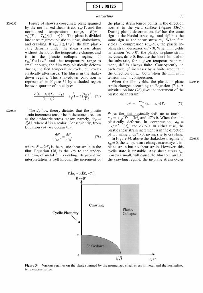
Figure 34 shows a coordinate plane spannedby the normalized shear stress, tm/Y, and thenormalized temperature range, Eðaf �asÞðTH � TLÞ=½ð1� nÞY : The plane is dividedinto three regimes: plastic collapse, shakedown,and crawling. If tm=YZ1=
ffiffiffi3
p; the film plasti-
cally deforms under the shear stress alonewithout the aid of the temperature change, andis in the plastic collapse regime. Iftm=Yo1=
ffiffiffi3
pand the temperature range is
small enough, the film may plastically deformduring the first temperature cycle, but cycleselastically afterwards. The film is in the shake-down regime. This shakedown condition isrepresented in Figure 34 by a shaded regionbelow a quarter of an ellipse:
Eðaf � asÞðTH � TLÞð1� nÞY ¼ 2
ffiffiffiffiffiffiffiffiffiffiffiffiffiffiffiffiffiffiffiffiffiffiffiffiffi1� 3
tmY
� �2r
: ð77Þ
The J2 flow theory dictates that the plasticstrain increment tensor be in the same directionas the deviatoric stress tensor, namely, deij ¼spijdl; where dl is a scalar. Consequently, fromEquation (74) we obtain that
dep
sm=3¼ dgp
2tm; ð78Þ
where gp ¼ 2ep13 is the plastic shear strain in thefilm. Equation (78) is the key to the under-standing of metal film crawling. Its geometricinterpretation is well known: the increment of
the plastic strain tensor points in the directionnormal to the yield surface (Figure 33(c)).During plastic deformation, dep has the samesign as the biaxial stress sm, and dgp has thesame sign as the shear stress tm. When filmyields in compression (smo0), the plastic in-plane strain decreases, depo0. When film yieldsin tension (sm40), the plastic in-plane strainincreases, dep40. Because the film is bonded tothe substrate, for a given temperature incre-ment, dep is always finite. Consequently, ineach cycle, gp increases by a finite amount inthe direction of tm, both when the film is intension and in compression.
When the film yields, the plastic in-planestrain changes according to Equation (71). Asubstitution into (78) gives the increment of theplastic shear strain:
dgp ¼ � 6tmsm
ðam � asÞ dT : ð79Þ
When the film plastically deforms in tension,sm ¼ þ
ffiffiffiffiffiffiffiffiffiffiffiffiffiffiffiffiffiffiffiffiY 2 � 3t2m
pand dTo0. When the film
plastically deforms in compression, sm ¼�
ffiffiffiffiffiffiffiffiffiffiffiffiffiffiffiffiffiffiffiffiY 2 � 3t2m
pand dT40. In either case, the
plastic shear strain increment is in the directionof tm, namely, dgp40, giving rise to crawling.
In Figure 34, above the shakedown regime, iftm¼ 0, the temperature change causes cyclic in-plane strain but no shear strain. However, thiscyclic state is unstable. Any shear stress tm,however small, will cause the film to crawl. Inthe crawling regime, the in-plane strain cycles
Figure 34 Various regimes on the plane spanned by the normalized shear stress in metal and the normalizedtemperature range.
SX0535
SX0536
SX0545
SX0550
Ratcheting 33
CSI : 08125
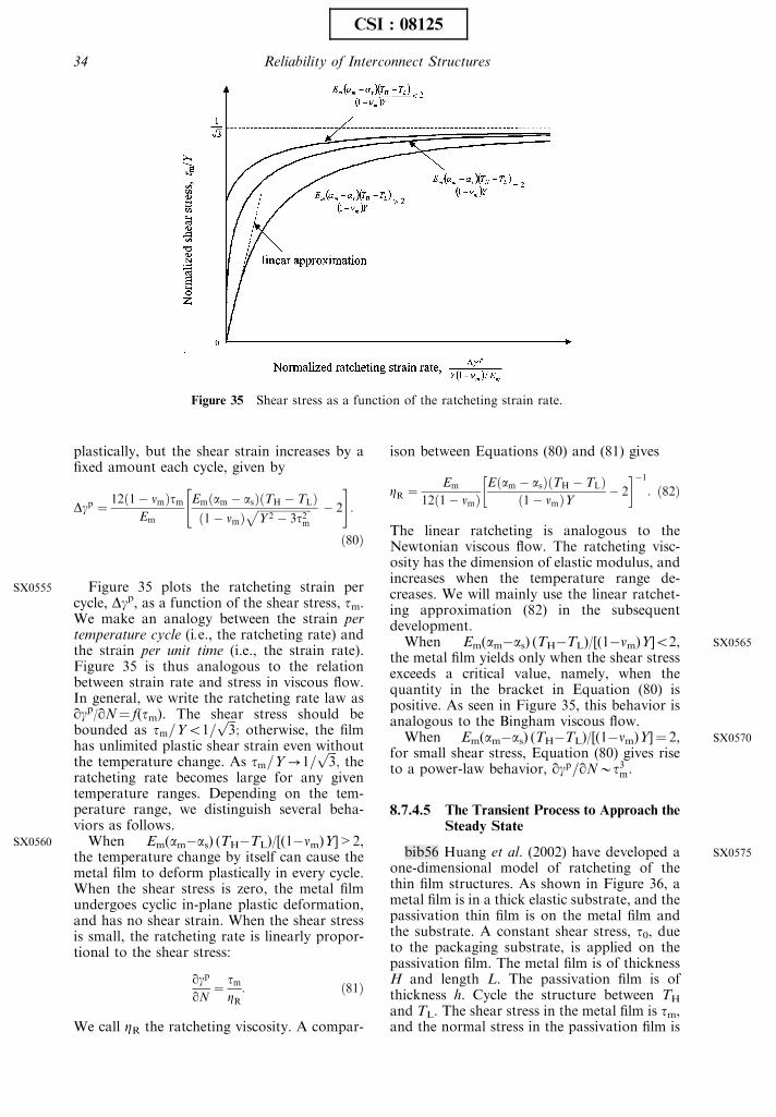
plastically, but the shear strain increases by afixed amount each cycle, given by
Dgp ¼ 12ð1� nmÞtmEm
Emðam � asÞðTH � TLÞð1� nmÞ
ffiffiffiffiffiffiffiffiffiffiffiffiffiffiffiffiffiffiffiffiY 2 � 3t2m
p � 2
" #:
ð80Þ
Figure 35 plots the ratcheting strain percycle, Dgp, as a function of the shear stress, tm.We make an analogy between the strain pertemperature cycle (i.e., the ratcheting rate) andthe strain per unit time (i.e., the strain rate).Figure 35 is thus analogous to the relationbetween strain rate and stress in viscous flow.In general, we write the ratcheting rate law asqgp/qN¼ f(tm). The shear stress should bebounded as tm=Yo1=
ffiffiffi3
p; otherwise, the film
has unlimited plastic shear strain even withoutthe temperature change. As tm=Y-1=
ffiffiffi3
p; the
ratcheting rate becomes large for any giventemperature ranges. Depending on the tem-perature range, we distinguish several beha-viors as follows.
When Em(am�as) (TH�TL)/[(1�nm)Y]>2,the temperature change by itself can cause themetal film to deform plastically in every cycle.When the shear stress is zero, the metal filmundergoes cyclic in-plane plastic deformation,and has no shear strain. When the shear stressis small, the ratcheting rate is linearly propor-tional to the shear stress:
qgp
qN¼ tm
ZR: ð81Þ
We call ZR the ratcheting viscosity. A compar-
ison between Equations (80) and (81) gives
ZR ¼ Em
12ð1� nmÞEðam � asÞðTH � TLÞ
ð1� nmÞY� 2
��1
: ð82Þ
The linear ratcheting is analogous to theNewtonian viscous flow. The ratcheting visc-osity has the dimension of elastic modulus, andincreases when the temperature range de-creases. We will mainly use the linear ratchet-ing approximation (82) in the subsequentdevelopment.
When Em(am�as) (TH�TL)/[(1�nm)Y]o2,the metal film yields only when the shear stressexceeds a critical value, namely, when thequantity in the bracket in Equation (80) ispositive. As seen in Figure 35, this behavior isanalogous to the Bingham viscous flow.
When Em(am�as) (TH�TL)/[(1�nm)Y]¼ 2,for small shear stress, Equation (80) gives riseto a power-law behavior, qgp=qNBt3m:
8.7.4.5 The Transient Process to Approach theSteady State
bib56 Huang et al. (2002) have developed aone-dimensional model of ratcheting of thethin film structures. As shown in Figure 36, ametal film is in a thick elastic substrate, and thepassivation thin film is on the metal film andthe substrate. A constant shear stress, t0, dueto the packaging substrate, is applied on thepassivation film. The metal film is of thicknessH and length L. The passivation film is ofthickness h. Cycle the structure between TH
and TL. The shear stress in the metal film is tm,and the normal stress in the passivation film is
Figure 35 Shear stress as a function of the ratcheting strain rate.
SX0555
SX0560
SX0565
SX0570
SX0575
34 Reliability of Interconnect Structures
CSI : 08125
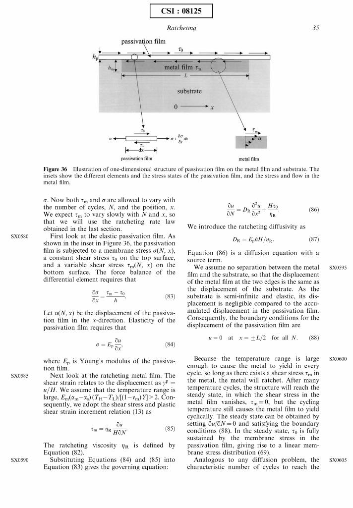
s. Now both tm and s are allowed to vary withthe number of cycles, N, and the position, x.We expect tm to vary slowly with N and x, sothat we will use the ratcheting rate lawobtained in the last section.
First look at the elastic passivation film. Asshown in the inset in Figure 36, the passivationfilm is subjected to a membrane stress s(N, x),a constant shear stress t0 on the top surface,and a variable shear stress tm(N, x) on thebottom surface. The force balance of thedifferential element requires that
qsqx
¼ tm � t0h
: ð83Þ
Let u(N, x) be the displacement of the passiva-tion film in the x-direction. Elasticity of thepassivation film requires that
s ¼ Epqu
qx; ð84Þ
where Ep is Young’s modulus of the passiva-tion film.
Next look at the ratcheting metal film. Theshear strain relates to the displacement as gp ¼u=H: We assume that the temperature range islarge, Em(am�as) (TH�TL)/[(1�nm)Y]>2. Con-sequently, we adopt the shear stress and plasticshear strain increment relation (13) as
tm ¼ ZRqu
HqN: ð85Þ
The ratcheting viscosity ZR is defined byEquation (82).
Substituting Equations (84) and (85) intoEquation (83) gives the governing equation:
qu
qN¼ DR
q2u
qx2þ Ht0
ZR: ð86Þ
We introduce the ratcheting diffusivity as
DR ¼ EphH=ZR: ð87Þ
Equation (86) is a diffusion equation with asource term.
We assume no separation between the metalfilm and the substrate, so that the displacementof the metal film at the two edges is the same asthe displacement of the substrate. As thesubstrate is semi-infinite and elastic, its dis-placement is negligible compared to the accu-mulated displacement in the passivation film.Consequently, the boundary conditions for thedisplacement of the passivation film are
u ¼ 0 at x ¼ 7L=2 for all N: ð88Þ
Because the temperature range is largeenough to cause the metal to yield in everycycle, so long as there exists a shear stress tm inthe metal, the metal will ratchet. After manytemperature cycles, the structure will reach thesteady state, in which the shear stress in themetal film vanishes, tm¼ 0, but the cyclingtemperature still causes the metal film to yieldcyclically. The steady state can be obtained bysetting qu/qN¼ 0 and satisfying the boundaryconditions (88). In the steady state, t0 is fullysustained by the membrane stress in thepassivation film, giving rise to a linear mem-brane stress distribution (69).
Analogous to any diffusion problem, thecharacteristic number of cycles to reach the
Figure 36 Illustration of one-dimensional structure of passivation film on the metal film and substrate. Theinsets show the different elements and the stress states of the passivation film, and the stress and flow in themetal film.
SX0580
SX0585
SX0590
SX0595
SX0600
SX0605
Ratcheting 35
CSI : 08125
steady state can be estimated by NC¼L2/DR,or
NC ¼ L2
hH
� �Em
12Epð1� nmÞ
� Emðam � afÞðTH � TLÞð1� nmÞY
� 2
��1
: ð89Þ
The number NC can be large mainly becausethe ratio L2/(hH) is large. If one replaces themetal film with a plastically deformable poly-mer, the ratio of elastic modulus of thepolymer and the passivation is small, whichwould significantly reduce NC. Note that NC isindependent of t0.
In the above, the metal film is taken to be anonhardening material in this model. Thiscorresponds to a safe engineering design, asthe hardening metal film can reduce theratcheting effects (bib55 Huang et al., 2001).The model can also be easily extended toconsider the nonlinearity of the ratchetingviscosity by using the finite difference method.The stress concentration at the edges needs tobe treated better, as the maximum tensile stressin the passivation film is at the corner. Fractureconditions also need to be considered morecarefully. Several useful rules for design areevident. First, one should aim to avoid metalfilm ratcheting altogether. Under cyclic tem-perature, the metal film cycles elastically if thetemperature range is small and the yieldstrength of the metal is large, according to(77). Second, if one cannot avoid ratcheting,one may aim to design the metal film geometrysuch that the passivation film can sustain thesteady state, in which the stress distribution inthe passivation film can be calculated bysolving a linear elastic plane-stress problem.Third, if the characteristic number NC is muchlarger than the number of cycles required bythe qualification test, one may design accord-ing to the transient stress state, solving thestress field as a function of the number ofcycles. The present model allows one toevaluate these options in design.
8.7.4.6 Ratcheting-induced Crack Growth
Consider the structure illustrated in Figure10 again. In the present context, a brittle filmlies on a metal underlayer, which in turn lies ona rigid substrate. Cycle the structure betweentemperatures TL and TH. Within the tempera-ture and time of the experiment, the metal doesnot creep, but can have time-independentplastic deformation. For simplicity, assumethat the tensile stress in the uncracked blanketfilm, s, is constant as the temperature changes.
This happens in practice when the elastic filmand the substrate have a similar coefficient ofthermal expansion, and s is due to thedeposition process or an applied load. Astemperature cycles, the metal layer undergoesratcheting plastic deformation. The stress fieldin the film relaxes in the crack wake, andintensifies around the crack tip. By theratcheting-creep analogy, we rewrite the scalinglaw for the crack velocity (38) as the scalinglaw for crack growth per cycle (bib78 Lianget al., 2002a):
da
dN¼ 0:6
Hhs2
ZRG; ð90Þ
where ZR is given by (82), and G is the fractureenergy of the brittle film.
8.7.5 STRESS-INDUCED VOIDING
This section begins with a description ofstress-induced voiding (SIV), followed by ananalysis of its main features: saturated voidvolume, resistance change, stress generation,void initiation, void growth, and stress relaxa-tion. We then give an analytical model ofnonhydrostatic stress state in an elastic–plasticinterconnect line encapsulated in a dielectric.An observation of SIV in blanket copper filmsis discussed. We finally consider the effects oflow-k dielectrics and barriers. bib98 Okabaya-shi (1993) and bib114 Sullivan (1996) haveprovided two reviews on SIV. This section willfocus on physical descriptions of the phenom-enon, leaving the design implications to thenext section, after we have studied electromi-gration.
8.7.5.1 Stress-Induced Voiding inEncapsulated Metal Line
Early aluminum lines had the width muchlarger than the thickness. They behaved likeblanket films. When narrow aluminum lineswere introduced, voids were observed onwafers held in ovens, or even on wafers lefton shelves at room temperature (bib24 Curryet al., 1984; bib140 Yue et al., 1985; bib128Turner and Wendel, 1985). The voids may becrack-like or rounded, grow with time, andsever the interconnects (Figure 37).
A basic understanding soon followed (bib64Jones and Basehore, 1987; bib45 Hinode et al.,1990; bib38 Greenebaum et al., 1991; bib68Korhonen et al., 1991; bib106 Sauter and Nix,1992). Aluminum has a larger thermal expan-sion coefficient than silica. Encapsulated insilica at a high temperature, on cooling, anarrow aluminum line is in a tensile, triaxial
SX0610
SX0615
SX0620
SX0625
SX0630
36 Reliability of Interconnect Structures
CSI : 08125
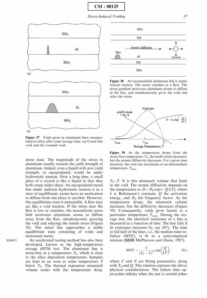
stress state. The magnitude of the stress inaluminum readily exceeds the yield strength ofaluminum. Indeed, even a liquid with zero yieldstrength, so encapsulated, would be underhydrostatic tension. Over a long time, a smallpiece of a crystal is like a liquid in that theyboth creep under shear. An encapsulated metalline under uniform hydrostatic tension is in astate of equilibrium: atoms have no motivationto diffuse from one place to another. However,this equilibrium state is metastable. A flaw mayact like a void nucleus. If the stress near theflaw is low or vanishes, the nonuniform stressfield motivates aluminum atoms to diffuseaway from the flaw, simultaneously growingthe void and relaxing the tensile stress (Figure38). The metal line approaches a stableequilibrium state consisting of voids andunstressed metal.
An accelerated testing method has also beendeveloped, known as the high-temperaturestorage (HTS) test. The aluminum line isstress-free at a temperature T0, which is closeto the silica deposition temperature. Samplesare kept in an oven at some temperature Tbelow T0. The thermal expansion mismatchvolume scales with the temperature drop,
T0�T. It is this mismatch volume that feedsto the void. The atomic diffusivity depends onthe temperature as D¼D0 exp (�Q/kT), wherek is Boltzmann’s constant, Q the activationenergy, and D0 the frequency factor. As thetemperature drops, the mismatch volumeincreases, but the diffusivity decreases (Figure39). Consequently, voids grow fastest at aparticular temperature Tmax. During the sto-rage test, the electrical resistance of a line ismeasured as a function of time. The line fails ifits resistance increases by, say 20%. The timeto fail half of the lines, i.e., the median-time-to-failure (MTF), is fit to a semi-empiricalrelation (bib90 McPherson and Dunn, 1987):
MTF ¼ C
ðT0 � TÞNexp
Q
kT
� �; ð91Þ
where C and N are fitting parameters, alongwith T0 and Q. This relation captures the abovephysical considerations. The failure time ap-proaches infinity when the test is carried either
Figure 37 Voids grow in aluminum lines encapsu-lated in silica after some storage time. (a) Crack-likevoid and (b) rounded void.
Figure 39 As the temperature drops from thestress-free temperature T0, the misfit strain increases,but the atomic diffusivity decreases. For a given timeduration, the void size maximizes at an intermediatetemperature Tmax.
Figure 38 An encapsulated aluminum line is undertriaxial tension. The stress vanishes at a flaw. Thestress gradient motivates aluminum atoms to diffusein the line, and simultaneously grow the void andrelax the stress.
SX0635
Stress-Induced Voiding 37
CSI : 08125
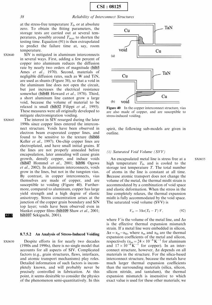
at the stress-free temperature T0, or at absolutezero. To obtain the fitting parameters, thestorage tests are carried out at several tem-peratures, possibly around Tmax to shorten thetesting time. Equation (91) is then extrapolatedto predict the failure time at, say, roomtemperature.
SIV is mitigated in aluminum interconnectsin several ways. First, adding a few percent ofcopper into aluminum reduces the diffusionrate by nearly two orders of magnitude (bib5Ames et al., 1970). Second, materials ofnegligible diffusion rates, such as W and TiN,are used as shunts (Figure 38), so that a void inthe aluminum line does not open the circuit,but just increases the electrical resistancesomewhat (bib48 Howard et al., 1978). Third,a short aluminum line cannot grow a largevoid, because the volume of material to berelaxed is small (bib32 Filippi et al., 1995).These measures were all originally developed tomitigate electromigration voiding.
The interest in SIV resurged during the later1990s since copper lines entered the intercon-nect structure. Voids have been observed inelectron beam evaporated copper lines, andfound to be sensitive to the texture (bib66Keller et al., 1997). On-chip copper lines areelectroplated, and have small initial grains. Ifthe lines are not properly annealed beforeencapsulation, later annealing will cause graingrowth, densify copper, and induce voids(bib47 Hommel et al., 2001; bib96 Ogawaet al., 2002). In aluminum interconnects, voidsgrow in the lines, but not in the tungsten vias.By contrast, in copper interconnects, viasthemselves are made of copper, and aresusceptible to voiding (Figure 40). Further-more, compared to aluminum, copper has largeyield strength and a high degree of elasticanisotropy. Stress concentration arises at thejunction of the copper grain boundary and SiNtop layer; voids have been observed even inblanket copper films (bib109 Shaw et al., 2001;bib107 Sekiguchi, 2001).
8.7.5.2 An Analysis of Stress-Induced Voiding
Despite efforts in for nearly two decades(1980s and 1990s), there is no single model thataccounts for all aspects of SIV. Complicatedfactors (e.g., grain structures, flaws, interfaces,and atomic transport mechanisms) play roles.Detailed information of such factors is incom-pletely known, and will probably never beprecisely controlled in fabrication. At thispoint, it seems desirable to consider the physicsof the phenomenon semi-quantitatively. In this
spirit, the following sub-models are given inoutline.
(i) Saturated Void Volume (SVV)
An encapsulated metal line is stress free at ahigh temperature T0, and is cooled to thestorage test temperature T. The total numberof atoms in the line is constant at all time.Because atomic transport does not change thevolume of the metal, the thermal misfit strain isaccommodated by a combination of void spaceand elastic deformation. When the stress in theline completely relaxes, the thermal expansionmisfit is fully accommodated by the void space.The saturated void volume (SVV) is
Vsn ¼ 3DaðT0 � TÞ V ; ð92Þ
where V is the volume of the metal line, and Dais the effective thermal expansion mismatchstrain. If a metal line were embedded in silicon,Da¼ am�aSi, where am and aSi are the thermalexpansion coefficients of the metal and silicon,respectively (am¼ 24� 10�6K�1 for aluminumand 17� 10�6K�1 for copper). In an inter-connect structure, however, Da depends on allmaterials in the structure. For the silica-basedinterconnect structure, because the metals havemuch larger thermal expansion coefficientsthan the surrounding materials (silica, silicon,silicon nitride, and tantalum), the thermalexpansion mismatch is insensitive to whichexact value is used for these other materials; we
Figure 40 In the copper interconnect structure, viasare also made of copper, and are susceptible tostress-induced voiding.
SX0640
SX0645
AU:5
SX0650
SX0655
38 Reliability of Interconnect Structures
CSI : 08125
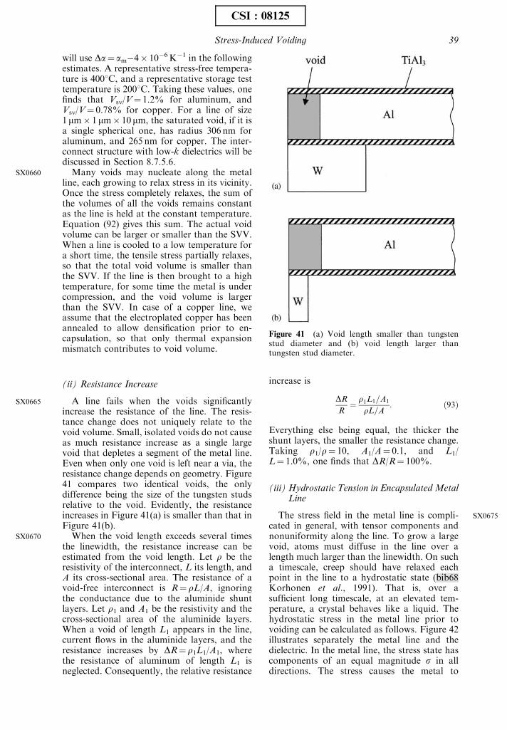
will use Da¼ am�4� 10�6K�1 in the followingestimates. A representative stress-free tempera-ture is 4001C, and a representative storage testtemperature is 2001C. Taking these values, onefinds that Vsn/V¼ 1.2% for aluminum, andVsn/V¼ 0.78% for copper. For a line of size1 mm� 1 mm� 10 mm, the saturated void, if it isa single spherical one, has radius 306 nm foraluminum, and 265 nm for copper. The inter-connect structure with low-k dielectrics will bediscussed in Section 8.7.5.6.
Many voids may nucleate along the metalline, each growing to relax stress in its vicinity.Once the stress completely relaxes, the sum ofthe volumes of all the voids remains constantas the line is held at the constant temperature.Equation (92) gives this sum. The actual voidvolume can be larger or smaller than the SVV.When a line is cooled to a low temperature fora short time, the tensile stress partially relaxes,so that the total void volume is smaller thanthe SVV. If the line is then brought to a hightemperature, for some time the metal is undercompression, and the void volume is largerthan the SVV. In case of a copper line, weassume that the electroplated copper has beenannealed to allow densification prior to en-capsulation, so that only thermal expansionmismatch contributes to void volume.
(ii) Resistance Increase
A line fails when the voids significantlyincrease the resistance of the line. The resis-tance change does not uniquely relate to thevoid volume. Small, isolated voids do not causeas much resistance increase as a single largevoid that depletes a segment of the metal line.Even when only one void is left near a via, theresistance change depends on geometry. Figure41 compares two identical voids, the onlydifference being the size of the tungsten studsrelative to the void. Evidently, the resistanceincreases in Figure 41(a) is smaller than that inFigure 41(b).
When the void length exceeds several timesthe linewidth, the resistance increase can beestimated from the void length. Let r be theresistivity of the interconnect, L its length, andA its cross-sectional area. The resistance of avoid-free interconnect is R¼ rL/A, ignoringthe conductance due to the aluminide shuntlayers. Let r1 and A1 be the resistivity and thecross-sectional area of the aluminide layers.When a void of length L1 appears in the line,current flows in the aluminide layers, and theresistance increases by DR¼ r1L1/A1, wherethe resistance of aluminum of length L1 isneglected. Consequently, the relative resistance
increase is
DR
R¼ r1L1=A1
rL=A: ð93Þ
Everything else being equal, the thicker theshunt layers, the smaller the resistance change.Taking r1/r¼ 10, A1/A¼ 0.1, and L1/L¼ 1.0%, one finds that DR/R¼ 100%.
(iii) Hydrostatic Tension in Encapsulated MetalLine
The stress field in the metal line is compli-cated in general, with tensor components andnonuniformity along the line. To grow a largevoid, atoms must diffuse in the line over alength much larger than the linewidth. On sucha timescale, creep should have relaxed eachpoint in the line to a hydrostatic state (bib68Korhonen et al., 1991). That is, over asufficient long timescale, at an elevated tem-perature, a crystal behaves like a liquid. Thehydrostatic stress in the metal line prior tovoiding can be calculated as follows. Figure 42illustrates separately the metal line and thedielectric. In the metal line, the stress state hascomponents of an equal magnitude s in alldirections. The stress causes the metal to
Figure 41 (a) Void length smaller than tungstenstud diameter and (b) void length larger thantungsten stud diameter.
SX0660
SX0665
SX0670
SX0675
Stress-Induced Voiding 39
CSI : 08125

expand with the volumetric elastic strain s/Bm,where Bm is the bulk modulus of the metal.When the metal is modeled as an isotropicmaterial, the bulk modulus relates to Young’smodulus Em and Poisson’s ratio nm asBm¼Em/3(1�2nm). For a metal of cubiccrystalline symmetry, the bulk modulus relatesto its crystalline elastic constants asBm¼ (C11þ 2C12)/3. For aluminum, C11 ¼108 GPa; C12 ¼ 62 GPa; C44 ¼ 28 GPa; giv-ing Bm¼ 77GPa. For Copper, C11 ¼168 GPa; C12 ¼ 121 GPa;C44 ¼ 75 GPa; giv-ing Bm¼ 136GPa.
Regard the encapsulation as an elastic solidwith a hole subject to a normal traction ofmagnitude s. The dielectric is in a state ofplane-strain deformation. The traction causesthe cross-sectional area of the hole to reduce byR
un ds; where un is the normal component ofthe elastic displacement at the hole surface. LetA be the cross-sectional area of the hole.Linearity of the elastic field requires that
1
A
Zun ds ¼ � s
meff: ð94Þ
This equation defines an effective modulus meff.This effective modulus depends on the shape ofthe hole, as well as the elastic constants of thedielectric, the barrier, and the silicon substrate.The effective modulus can be readily calculatedusing the finite element method (Section8.7.5.6). If the cross-section is a long rectangle,rather than a square, the system is morecompliant, leading to a small meff. In theidealized case, when the hole has a circularcross-section, and the dielectric is infinite, thestress field in the dielectric is known analyti-cally, and we find that the effective modulus ismeff¼Ed/2(1þ nd), coincident with the shearmodulus of the dielectric.
Let y be the volumetric strain caused, e.g., bythe mismatch in thermal expansion coefficients,or densification, or atomic diffusion. Thisvolumetric strain is accommodated by thedifference in the volume change of the inter-connect line and that of the dielectric hole.Combining the two contributions, one relatesthe hydrostatic stress in the metal, s, to thevolumetric mismatch strain between the metaland the encapsulation, y, namely,
s ¼ By; ð95Þ
with the effective modulus B given by
1
B¼ 1
Bmþ 1
meff: ð96Þ
If the cross-section is a long rectangle, theeffective modus is small, leading to a lowhydrostatic stress. In the limiting case when theinterconnect is a blanket film, the hydrostaticstress vanishes in this liquid-like model. For aninterconnect of a square cross-section, takingmeff¼ 30GPa for silica, the effective modulus isB¼ 22GPa for aluminum/silica structure, andB¼ 24GPa for copper/silica structure. Themismatch strain is mainly accommodated bythe elastic deformation of the dielectric, so thatthe effective moduli of the two structures aresimilar, despite the nearly factor 2 difference inthe bulk moduli of aluminum and copper. Theeffective modulus reduces if the cross-section isa long rectangle. Assume that the volumetricstrain is entirely due to the thermal expansionmismatch between the metal and the dielectric,y¼ 3Da(T0�T). For the temperature drop T0 �T¼ 200K, the hydrostatic stress iss¼ 260MPa in aluminum line, ands¼ 187MPa in copper line. Some authorshave treated the dielectric as a rigid material,and taken the bulk modulus of the metal, Bm,as the effective modulus. This would signifi-cantly overestimate the effective modulus (Bm/B¼ 3.5 for aluminum and Bm/B¼ 5.7 forcopper).
Figure 42 Consider separately the metal line as acylinder and the dielectric as a solid with a hole.
SX0680
SX0685
40 Reliability of Interconnect Structures
CSI : 08125
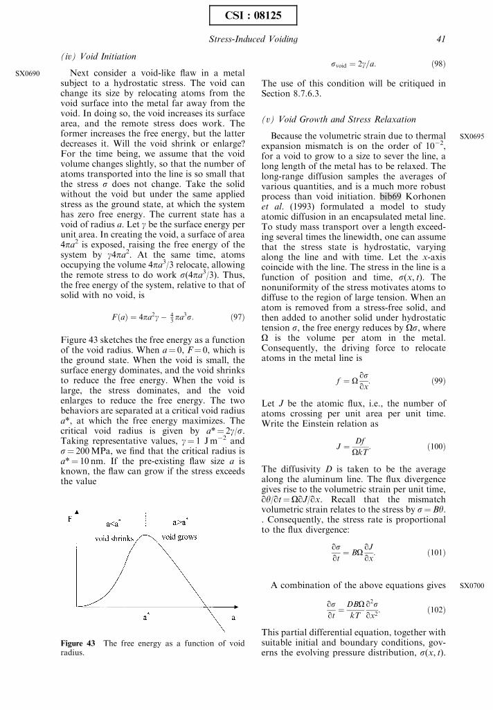
(iv) Void Initiation
Next consider a void-like flaw in a metalsubject to a hydrostatic stress. The void canchange its size by relocating atoms from thevoid surface into the metal far away from thevoid. In doing so, the void increases its surfacearea, and the remote stress does work. Theformer increases the free energy, but the latterdecreases it. Will the void shrink or enlarge?For the time being, we assume that the voidvolume changes slightly, so that the number ofatoms transported into the line is so small thatthe stress s does not change. Take the solidwithout the void but under the same appliedstress as the ground state, at which the systemhas zero free energy. The current state has avoid of radius a. Let g be the surface energy perunit area. In creating the void, a surface of area4pa2 is exposed, raising the free energy of thesystem by g4pa2. At the same time, atomsoccupying the volume 4pa3/3 relocate, allowingthe remote stress to do work s(4pa3/3). Thus,the free energy of the system, relative to that ofsolid with no void, is
FðaÞ ¼ 4pa2g� 43 pa3s: ð97Þ
Figure 43 sketches the free energy as a functionof the void radius. When a¼ 0, F¼ 0, which isthe ground state. When the void is small, thesurface energy dominates, and the void shrinksto reduce the free energy. When the void islarge, the stress dominates, and the voidenlarges to reduce the free energy. The twobehaviors are separated at a critical void radiusa*, at which the free energy maximizes. Thecritical void radius is given by a*¼ 2g/s.Taking representative values, g¼ 1 Jm�2 ands¼ 200MPa, we find that the critical radius isa*¼ 10 nm. If the pre-existing flaw size a isknown, the flaw can grow if the stress exceedsthe value
svoid ¼ 2g=a: ð98Þ
The use of this condition will be critiqued inSection 8.7.6.3.
(v) Void Growth and Stress Relaxation
Because the volumetric strain due to thermalexpansion mismatch is on the order of 10�2,for a void to grow to a size to sever the line, along length of the metal has to be relaxed. Thelong-range diffusion samples the averages ofvarious quantities, and is a much more robustprocess than void initiation. bib69 Korhonenet al. (1993) formulated a model to studyatomic diffusion in an encapsulated metal line.To study mass transport over a length exceed-ing several times the linewidth, one can assumethat the stress state is hydrostatic, varyingalong the line and with time. Let the x-axiscoincide with the line. The stress in the line is afunction of position and time, s(x, t). Thenonuniformity of the stress motivates atoms todiffuse to the region of large tension. When anatom is removed from a stress-free solid, andthen added to another solid under hydrostatictension s, the free energy reduces by Os, whereO is the volume per atom in the metal.Consequently, the driving force to relocateatoms in the metal line is
f ¼ Oqsqx
: ð99Þ
Let J be the atomic flux, i.e., the number ofatoms crossing per unit area per unit time.Write the Einstein relation as
J ¼ Df
OkT: ð100Þ
The diffusivity D is taken to be the averagealong the aluminum line. The flux divergencegives rise to the volumetric strain per unit time,qy/qt¼OqJ/qx. Recall that the mismatchvolumetric strain relates to the stress by s¼By.. Consequently, the stress rate is proportionalto the flux divergence:
qsqt
¼ BOqJ
qx: ð101Þ
A combination of the above equations gives
qsqt
¼ DBOkT
q2sqx2
: ð102Þ
This partial differential equation, together withsuitable initial and boundary conditions, gov-erns the evolving pressure distribution, s(x, t).
Figure 43 The free energy as a function of voidradius.
SX0690
SX0695
SX0700
Stress-Induced Voiding 41
CSI : 08125
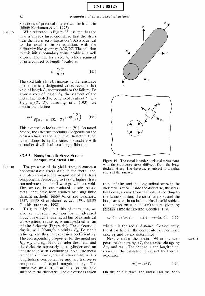
Solutions of practical interest can be found in(bib69 Korhonen et al., 1993).
With reference to Figure 38, assume that theflaw is already large enough so that the stressnear the flaw is zero. Equation (102) is identicalto the usual diffusion equation, with thediffusivity-like quantity DBO/kT. The solutionto this initial-boundary value problem is wellknown. The time for a void to relax a segmentof interconnect of length l scales as
tlBl2kT
DBO: ð103Þ
The void fails a line by increasing the resistanceof the line to a designated value. Assume thatvoid of length L1 corresponds to the failure. Togrow a void of length L1, the segment of themetal line needed to be relaxed is about l¼L1/3(am�ad)(T0�T). Inserting into (103), weobtain the lifetime
tlifep1
B½ðam � adÞðT0 � TÞ2exp
Q
kT
� �: ð104Þ
This expression looks similar to (91). As notedbefore, the effective modulus B depends on thecross-section shape and the dielectric type.Other things being the same, a structure witha smaller B will lead to a longer lifetime.
8.7.5.3 Nonhydrostatic Stress State inEncapsulated Metal Line
The presence of the yield strength causes anonhydrostatic stress state in the metal line,and also increases the magnitude of all stresscomponents. According to (98), a higher stresscan activate a smaller flaw to grow into a void.The stresses in encapsulated elastic plasticmetal lines have been studied by using finiteelement methods (bib64 Jones and Basehore,1987; bib38 Greenebaum et al., 1991; bib37Gouldstone et al., 1998).
To gain insight into this phenomenon, wegive an analytical solution for an idealizedmodel, in which a long metal line of cylindricalcross-section, radius a, is encapsulated in aninfinite dielectric (Figure 44). The dielectric iselastic, with Young’s modulus Ed, Poisson’sratio nd, and thermal expansion coefficient ad.The corresponding properties for the metal areEm, nm, and am. Now consider the metal andthe dielectric separately as a cylinder and aninfinite solid with a cylindrical hole. The metalis under a uniform, triaxial stress field, with alongitudinal component sL and two transversecomponents of equal magnitude sT. Thetransverse stress sT also acts on the holesurface in the dielectric. The dielectric is taken
to be infinite, and the longitudinal stress in thedielectric is zero. Inside the dielectric, the stressfield decays away from the hole. According tothe Lame solution, the radial stress sr and thehoop stress sy in an infinite elastic solid subjectto a stress on a hole surface are given by(bib127 Timoshenko and Goodier, 1970)
srðrÞ ¼ sTða=rÞ2; syðrÞ ¼ �sTða=rÞ2; ð105Þ
where r is the radial distance. Consequently,the stress field in the composite is determinedonce sL and sT are determined.
Next consider the strains. When the tem-perature changes by DT, the stresses change byDsT and DsL. The change in the longitudinalstrain in the dielectric is caused by thermalexpansion:
DedL ¼ adDT : ð106Þ
On the hole surface, the radial and the hoop
Figure 44 The metal is under a triaxial stress state,with the transverse stress different from the long-itudinal stress. The dielectric is subject to a radialstress at the surface.
SX0705
SX0710
SX0715
SX0716
42 Reliability of Interconnect Structures
CSI : 08125
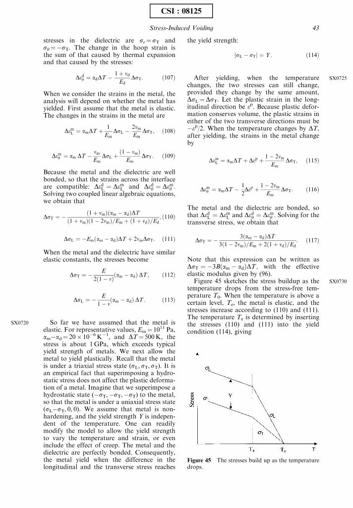
stresses in the dielectric are sr¼ sT andsy¼�sT. The change in the hoop strain isthe sum of that caused by thermal expansionand that caused by the stresses:
Dedy ¼ adDT � 1þ ndEd
DsT: ð107Þ
When we consider the strains in the metal, theanalysis will depend on whether the metal hasyielded. First assume that the metal is elastic.The changes in the strains in the metal are
DemL ¼ amDT þ 1
EmDsL � 2nm
EmDsT; ð108Þ
Demy ¼ am DT � nmEm
DsL þ ð1� nmÞEm
DsT: ð109Þ
Because the metal and the dielectric are wellbonded, so that the strains across the interfaceare compatible: DedL ¼ DemL and Dedy ¼ Demy :Solving two coupled linear algebraic equations,we obtain that
DsT ¼ � ð1þ nmÞðam � adÞDT
ð1þ nmÞð1� 2nmÞ=Em þ ð1þ ndÞ=Ed; ð110Þ
DsL ¼ �Emðam � adÞDT þ 2nmDsT: ð111Þ
When the metal and the dielectric have similarelastic constants, the stresses become
DsT ¼ � E
2ð1� nÞðam � adÞ DT ; ð112Þ
DsL ¼ � E
1� nðam � adÞ DT : ð113Þ
So far we have assumed that the metal iselastic. For representative values, Em¼ 1011 Pa,am�ad¼ 20� 10�6K�1, and DT¼ 500K, thestress is about 1GPa, which exceeds typicalyield strength of metals. We next allow themetal to yield plastically. Recall that the metalis under a triaxial stress state (sL, sT, sT). It isan empirical fact that superimposing a hydro-static stress does not affect the plastic deforma-tion of a metal. Imagine that we superimpose ahydrostatic state (�sT,�sT,�sT) to the metal,so that the metal is under a uniaxial stress state(sL�sT, 0, 0). We assume that metal is non-hardening, and the yield strength Y is indepen-dent of the temperature. One can readilymodify the model to allow the yield strengthto vary the temperature and strain, or eveninclude the effect of creep. The metal and thedielectric are perfectly bonded. Consequently,the metal yield when the difference in thelongitudinal and the transverse stress reaches
the yield strength:
jsL � sTj ¼ Y : ð114Þ
After yielding, when the temperaturechanges, the two stresses can still change,provided they change by the same amount,DsL¼DsT. Let the plastic strain in the long-itudinal direction be ep. Because plastic defor-mation conserves volume, the plastic strains ineither of the two transverse directions must be�ep/2. When the temperature changes by DT,after yielding, the strains in the metal changeby
DemL ¼ amDT þ Dep þ 1� 2nmEm
DsT; ð115Þ
Demy ¼ amDT � 1
2Dep þ 1� 2nm
EmDsT: ð116Þ
The metal and the dielectric are bonded, sothat DedL ¼ DemL and Dedy ¼ Demy : Solving for thetransverse stress, we obtain that
DsT ¼ � 3ðam � adÞDT
3ð1� 2nmÞ=Em þ 2ð1þ ndÞ=Ed: ð117Þ
Note that this expression can be written asDsT ¼ �3Bðam � adÞDT ; with the effectiveelastic modulus given by (96).
Figure 45 sketches the stress buildup as thetemperature drops from the stress-free tem-perature T0. When the temperature is above acertain level, Te, the metal is elastic, and thestresses increase according to (110) and (111).The temperature Te is determined by insertingthe stresses (110) and (111) into the yieldcondition (114), giving
Figure 45 The stresses build up as the temperaturedrops.
SX0720
SX0725
SX0730
Stress-Induced Voiding 43
CSI : 08125
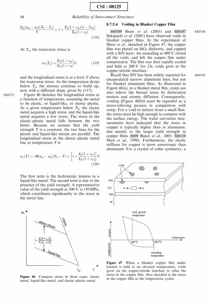
Emðam � adÞðT0 � TeÞY
¼ 1þ Edð1þ nmÞð1� 2nmÞEmð1þ ndÞ
:
ð118Þ
At Te, the transverse stress is
sTðTeÞ ¼Edð1þ nmÞEmð1þ ndÞ
Y ; ð119Þ
and the longitudinal stress is at a level Y abovethe transverse stress. As the temperature dropsbelow Te, the stresses continue to build up,now with a different slope, given by (117).
Figure 46 sketches the longitudinal stress asa function of temperature, assuming the metalto be elastic, or liquid-like, or elastic–plastic.At a given temperature below T0, the elasticmetal acquires a high stress, and the liquid-likemetal acquires a low stress. The stress in theelastic–plastic metal falls between the twolimits. Because we assume that the yieldstrength Y is a constant, the two lines for theplastic and liquid-like metals are parallel. Thelongitudinal stress in the elastic–plastic metalline at temperature T is
sLðTÞ ¼ 3Bðam � adÞðT0 � TÞ þ 1þ Edð1þ nmÞEmð1þ ndÞ
�Y :
ð120Þ
The first term is the hydrostatic tension in aliquid-like metal. The second term is due to thepresence of the yield strength. A representativevalue of the yield strength at 2001C is 150MPa,which contributes significantly to the stress inthe metal line.
8.7.5.4 Voiding in Blanket Copper Film
bib109 Shaw et al. (2001) and bib107Sekiguchi et al. (2001) have observed voids inblanket copper films. In the experiment ofShaw et al., sketched in Figure 47, the copperfilm was plated on SiO2 dielectric, and cappedwith a SiN layer. An annealing at 4001C closedall the voids, and left the copper film undercompression. The film was then rapidly cooledand held at 2001C for 2 h; voids grew at thecopper/nitride interface.
Recall that SIV has been widely reported forencapsulated narrow aluminum lines, but notfor blanket aluminum films. As illustrated inFigure 48(a), in a blanket metal film, creep canalso relieve the biaxial stress by dislocationmotion and atomic diffusion. Consequently,voiding (Figure 48(b)) must be regarded as astress-relieving process in competition withcreep. For a void to initiate from a small flaw,the stress must be high enough to compete withthe surface energy. The wafer curvature mea-surements have indicated that the stress incopper is typically higher than in aluminum,due mainly to the larger yield strength incopper films (bib9 Baker et al., 2001; bib110Shen et al., 1998). Furthermore, the elasticstiffness for copper is more anisotropic thanaluminum. For a crystal of cubic symmetry, a
Figure 46 Compare stress in three cases: elasticmetal, liquid-like metal, and elastic–plastic metal.
Figure 47 When a blanket copper film undertension is held at an elevated temperature, voidsgrow on the copper/nitride interface to relax thestress in the copper film. Also sketched is the stressin the copper film as the temperature cycles.
SX0735
SX0740
SX0745
44 Reliability of Interconnect Structures
CSI : 08125
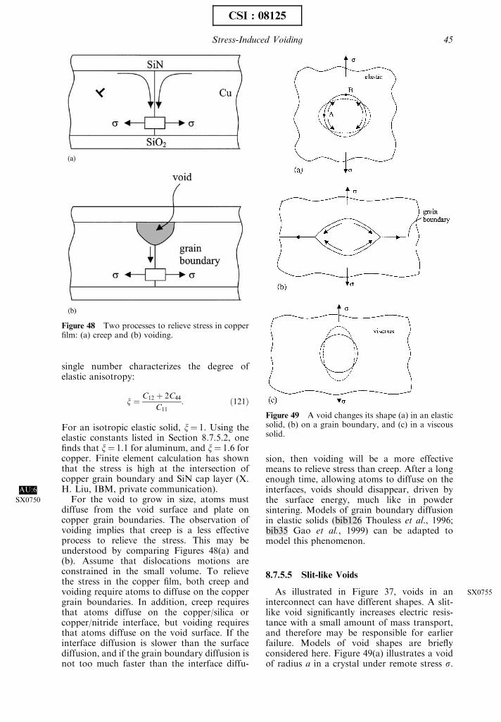
single number characterizes the degree ofelastic anisotropy:
x ¼ C12 þ 2C44
C11: ð121Þ
For an isotropic elastic solid, x¼ 1. Using theelastic constants listed in Section 8.7.5.2, onefinds that x¼ 1.1 for aluminum, and x¼ 1.6 forcopper. Finite element calculation has shownthat the stress is high at the intersection ofcopper grain boundary and SiN cap layer (X.H. Liu, IBM, private communication).
For the void to grow in size, atoms mustdiffuse from the void surface and plate oncopper grain boundaries. The observation ofvoiding implies that creep is a less effectiveprocess to relieve the stress. This may beunderstood by comparing Figures 48(a) and(b). Assume that dislocations motions areconstrained in the small volume. To relievethe stress in the copper film, both creep andvoiding require atoms to diffuse on the coppergrain boundaries. In addition, creep requiresthat atoms diffuse on the copper/silica orcopper/nitride interface, but voiding requiresthat atoms diffuse on the void surface. If theinterface diffusion is slower than the surfacediffusion, and if the grain boundary diffusion isnot too much faster than the interface diffu-
sion, then voiding will be a more effectivemeans to relieve stress than creep. After a longenough time, allowing atoms to diffuse on theinterfaces, voids should disappear, driven bythe surface energy, much like in powdersintering. Models of grain boundary diffusionin elastic solids (bib126 Thouless et al., 1996;bib35 Gao et al., 1999) can be adapted tomodel this phenomenon.
8.7.5.5 Slit-like Voids
As illustrated in Figure 37, voids in aninterconnect can have different shapes. A slit-like void significantly increases electric resis-tance with a small amount of mass transport,and therefore may be responsible for earlierfailure. Models of void shapes are brieflyconsidered here. Figure 49(a) illustrates a voidof radius a in a crystal under remote stress s.
Figure 48 Two processes to relieve stress in copperfilm: (a) creep and (b) voiding.
Figure 49 A void changes its shape (a) in an elasticsolid, (b) on a grain boundary, and (c) in a viscoussolid.
AU:6
SX0750
SX0755
Stress-Induced Voiding 45
CSI : 08125
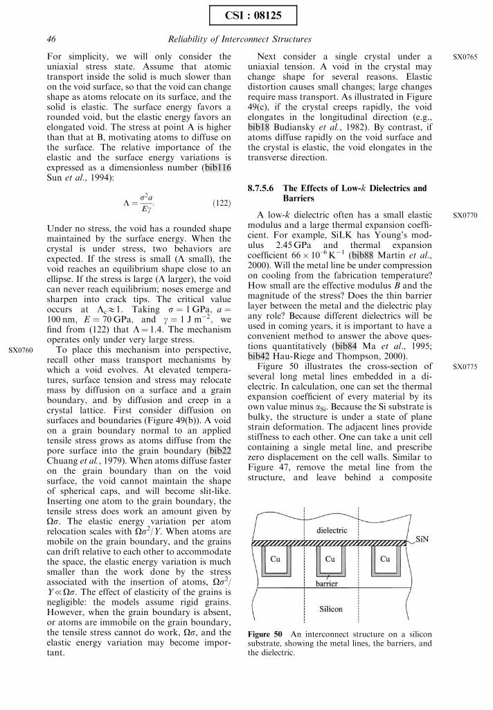
For simplicity, we will only consider theuniaxial stress state. Assume that atomictransport inside the solid is much slower thanon the void surface, so that the void can changeshape as atoms relocate on its surface, and thesolid is elastic. The surface energy favors arounded void, but the elastic energy favors anelongated void. The stress at point A is higherthan that at B, motivating atoms to diffuse onthe surface. The relative importance of theelastic and the surface energy variations isexpressed as a dimensionless number (bib116Sun et al., 1994):
L ¼ s2a
Eg: ð122Þ
Under no stress, the void has a rounded shapemaintained by the surface energy. When thecrystal is under stress, two behaviors areexpected. If the stress is small (L small), thevoid reaches an equilibrium shape close to anellipse. If the stress is large (L larger), the voidcan never reach equilibrium; noses emerge andsharpen into crack tips. The critical valueoccurs at LcE1. Taking s ¼ 1 GPa; a ¼100 nm; E ¼ 70 GPa; and g ¼ 1 J m�2; wefind from (122) that L¼ 1.4. The mechanismoperates only under very large stress.
To place this mechanism into perspective,recall other mass transport mechanisms bywhich a void evolves. At elevated tempera-tures, surface tension and stress may relocatemass by diffusion on a surface and a grainboundary, and by diffusion and creep in acrystal lattice. First consider diffusion onsurfaces and boundaries (Figure 49(b)). A voidon a grain boundary normal to an appliedtensile stress grows as atoms diffuse from thepore surface into the grain boundary (bib22Chuang et al., 1979). When atoms diffuse fasteron the grain boundary than on the voidsurface, the void cannot maintain the shapeof spherical caps, and will become slit-like.Inserting one atom to the grain boundary, thetensile stress does work an amount given byOs. The elastic energy variation per atomrelocation scales with Os2/Y. When atoms aremobile on the grain boundary, and the grainscan drift relative to each other to accommodatethe space, the elastic energy variation is muchsmaller than the work done by the stressassociated with the insertion of atoms, Os2/Y{Os. The effect of elasticity of the grains isnegligible: the models assume rigid grains.However, when the grain boundary is absent,or atoms are immobile on the grain boundary,the tensile stress cannot do work, Os, and theelastic energy variation may become impor-tant.
Next consider a single crystal under auniaxial tension. A void in the crystal maychange shape for several reasons. Elasticdistortion causes small changes; large changesrequire mass transport. As illustrated in Figure49(c), if the crystal creeps rapidly, the voidelongates in the longitudinal direction (e.g.,bib18 Budiansky et al., 1982). By contrast, ifatoms diffuse rapidly on the void surface andthe crystal is elastic, the void elongates in thetransverse direction.
8.7.5.6 The Effects of Low-k Dielectrics andBarriers
A low-k dielectric often has a small elasticmodulus and a large thermal expansion coeffi-cient. For example, SiLK has Young’s mod-ulus 2.45GPa and thermal expansioncoefficient 66� 10–6K�1 (bib88 Martin et al.,2000). Will the metal line be under compressionon cooling from the fabrication temperature?How small are the effective modulus B and themagnitude of the stress? Does the thin barrierlayer between the metal and the dielectric playany role? Because different dielectrics will beused in coming years, it is important to have aconvenient method to answer the above ques-tions quantitatively (bib84 Ma et al., 1995;bib42 Hau-Riege and Thompson, 2000).
Figure 50 illustrates the cross-section ofseveral long metal lines embedded in a di-electric. In calculation, one can set the thermalexpansion coefficient of every material by itsown value minus aSi. Because the Si substrate isbulky, the structure is under a state of planestrain deformation. The adjacent lines providestiffness to each other. One can take a unit cellcontaining a single metal line, and prescribezero displacement on the cell walls. Similar toFigure 47, remove the metal line from thestructure, and leave behind a composite
Figure 50 An interconnect structure on a siliconsubstrate, showing the metal lines, the barriers, andthe dielectric.
SX0760
SX0765
SX0770
SX0775
46 Reliability of Interconnect Structures
CSI : 08125
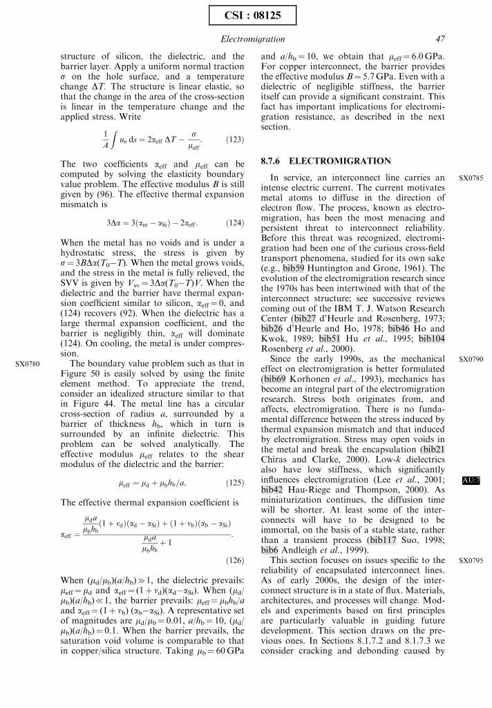
structure of silicon, the dielectric, and thebarrier layer. Apply a uniform normal tractions on the hole surface, and a temperaturechange DT. The structure is linear elastic, sothat the change in the area of the cross-sectionis linear in the temperature change and theapplied stress. Write
1
A
Zun ds ¼ 2aeff DT � s
meff: ð123Þ
The two coefficients aeff and meff can becomputed by solving the elasticity boundaryvalue problem. The effective modulus B is stillgiven by (96). The effective thermal expansionmismatch is
3Da ¼ 3ðam � aSiÞ � 2aeff : ð124Þ
When the metal has no voids and is under ahydrostatic stress, the stress is given bys¼ 3BDa(T0�T). When the metal grows voids,and the stress in the metal is fully relieved, theSVV is given by Vsv¼ 3Da(T0�T)V. When thedielectric and the barrier have thermal expan-sion coefficient similar to silicon, aeff¼ 0, and(124) recovers (92). When the dielectric has alarge thermal expansion coefficient, and thebarrier is negligibly thin, aeff will dominate(124). On cooling, the metal is under compres-sion.
The boundary value problem such as that inFigure 50 is easily solved by using the finiteelement method. To appreciate the trend,consider an idealized structure similar to thatin Figure 44. The metal line has a circularcross-section of radius a, surrounded by abarrier of thickness hb, which in turn issurrounded by an infinite dielectric. Thisproblem can be solved analytically. Theeffective modulus meff relates to the shearmodulus of the dielectric and the barrier:
meff ¼ md þ mbhb=a; ð125Þ
The effective thermal expansion coefficient is
aeff ¼
mda
mbhbð1þ ndÞðad � aSiÞ þ ð1þ nbÞðab � aSiÞ
mda
mbhbþ 1
:
ð126Þ
When (md/mb)(a/hb)c1, the dielectric prevails:meff¼ md and aeff¼ (1þ nd)(ad�aSi). When (md/mb)(a/hb){1, the barrier prevails: meff¼ mbhb/aand aeff¼ (1þ nb) (ab�aSi). A representative setof magnitudes are md/mb¼ 0.01, a/hb¼ 10, (md/mb)(a/hb)¼ 0.1. When the barrier prevails, thesaturation void volume is comparable to thatin copper/silica structure. Taking mb¼ 60GPa
and a/hb¼ 10, we obtain that meff¼ 6.0GPa.For copper interconnect, the barrier providesthe effective modulus B¼ 5.7GPa. Even with adielectric of negligible stiffness, the barrieritself can provide a significant constraint. Thisfact has important implications for electromi-gration resistance, as described in the nextsection.
8.7.6 ELECTROMIGRATION
In service, an interconnect line carries anintense electric current. The current motivatesmetal atoms to diffuse in the direction ofelectron flow. The process, known as electro-migration, has been the most menacing andpersistent threat to interconnect reliability.Before this threat was recognized, electromi-gration had been one of the curious cross-fieldtransport phenomena, studied for its own sake(e.g., bib59 Huntington and Grone, 1961). Theevolution of the electromigration research sincethe 1970s has been intertwined with that of theinterconnect structure; see successive reviewscoming out of the IBM T. J. Watson ResearchCenter (bib27 d’Heurle and Rosenberg, 1973;bib26 d’Heurle and Ho, 1978; bib46 Ho andKwok, 1989; bib51 Hu et al., 1995; bib104Rosenberg et al., 2000).
Since the early 1990s, as the mechanicaleffect on electromigration is better formulated(bib69 Korhonen et al., 1993), mechanics hasbecome an integral part of the electromigrationresearch. Stress both originates from, andaffects, electromigration. There is no funda-mental difference between the stress induced bythermal expansion mismatch and that inducedby electromigration. Stress may open voids inthe metal and break the encapsulation (bib21Chiras and Clarke, 2000). Low-k dielectricsalso have low stiffness, which significantlyinfluences electromigration (Lee et al., 2001;bib42 Hau-Riege and Thompson, 2000). Asminiaturization continues, the diffusion timewill be shorter. At least some of the inter-connects will have to be designed to beimmortal, on the basis of a stable state, ratherthan a transient process (bib117 Suo, 1998;bib6 Andleigh et al., 1999).
This section focuses on issues specific to thereliability of encapsulated interconnect lines.As of early 2000s, the design of the inter-connect structure is in a state of flux. Materials,architectures, and processes will change. Mod-els and experiments based on first principlesare particularly valuable in guiding futuredevelopment. This section draws on the pre-vious ones. In Sections 8.1.7.2 and 8.1.7.3 weconsider cracking and debonding caused by
SX0780
SX0785
SX0790
AU:7
SX0795
Electromigration 47
CSI : 08125
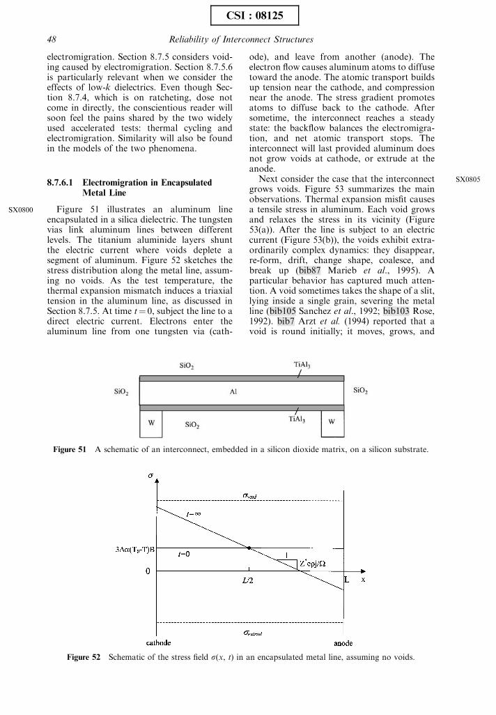
electromigration. Section 8.7.5 considers void-ing caused by electromigration. Section 8.7.5.6is particularly relevant when we consider theeffects of low-k dielectrics. Even though Sec-tion 8.7.4, which is on ratcheting, dose notcome in directly, the conscientious reader willsoon feel the pains shared by the two widelyused accelerated tests: thermal cycling andelectromigration. Similarity will also be foundin the models of the two phenomena.
8.7.6.1 Electromigration in EncapsulatedMetal Line
Figure 51 illustrates an aluminum lineencapsulated in a silica dielectric. The tungstenvias link aluminum lines between differentlevels. The titanium aluminide layers shuntthe electric current where voids deplete asegment of aluminum. Figure 52 sketches thestress distribution along the metal line, assum-ing no voids. As the test temperature, thethermal expansion mismatch induces a triaxialtension in the aluminum line, as discussed inSection 8.7.5. At time t¼ 0, subject the line to adirect electric current. Electrons enter thealuminum line from one tungsten via (cath-
ode), and leave from another (anode). Theelectron flow causes aluminum atoms to diffusetoward the anode. The atomic transport buildsup tension near the cathode, and compressionnear the anode. The stress gradient promotesatoms to diffuse back to the cathode. Aftersometime, the interconnect reaches a steadystate: the backflow balances the electromigra-tion, and net atomic transport stops. Theinterconnect will last provided aluminum doesnot grow voids at cathode, or extrude at theanode.
Next consider the case that the interconnectgrows voids. Figure 53 summarizes the mainobservations. Thermal expansion misfit causesa tensile stress in aluminum. Each void growsand relaxes the stress in its vicinity (Figure53(a)). After the line is subject to an electriccurrent (Figure 53(b)), the voids exhibit extra-ordinarily complex dynamics: they disappear,re-form, drift, change shape, coalesce, andbreak up (bib87 Marieb et al., 1995). Aparticular behavior has captured much atten-tion. A void sometimes takes the shape of a slit,lying inside a single grain, severing the metalline (bib105 Sanchez et al., 1992; bib103 Rose,1992). bib7 Arzt et al. (1994) reported that avoid is round initially; it moves, grows, and
Figure 52 Schematic of the stress field s(x, t) in an encapsulated metal line, assuming no voids.
Figure 51 A schematic of an interconnect, embedded in a silicon dioxide matrix, on a silicon substrate.
SX0800
SX0805
48 Reliability of Interconnect Structures
CSI : 08125
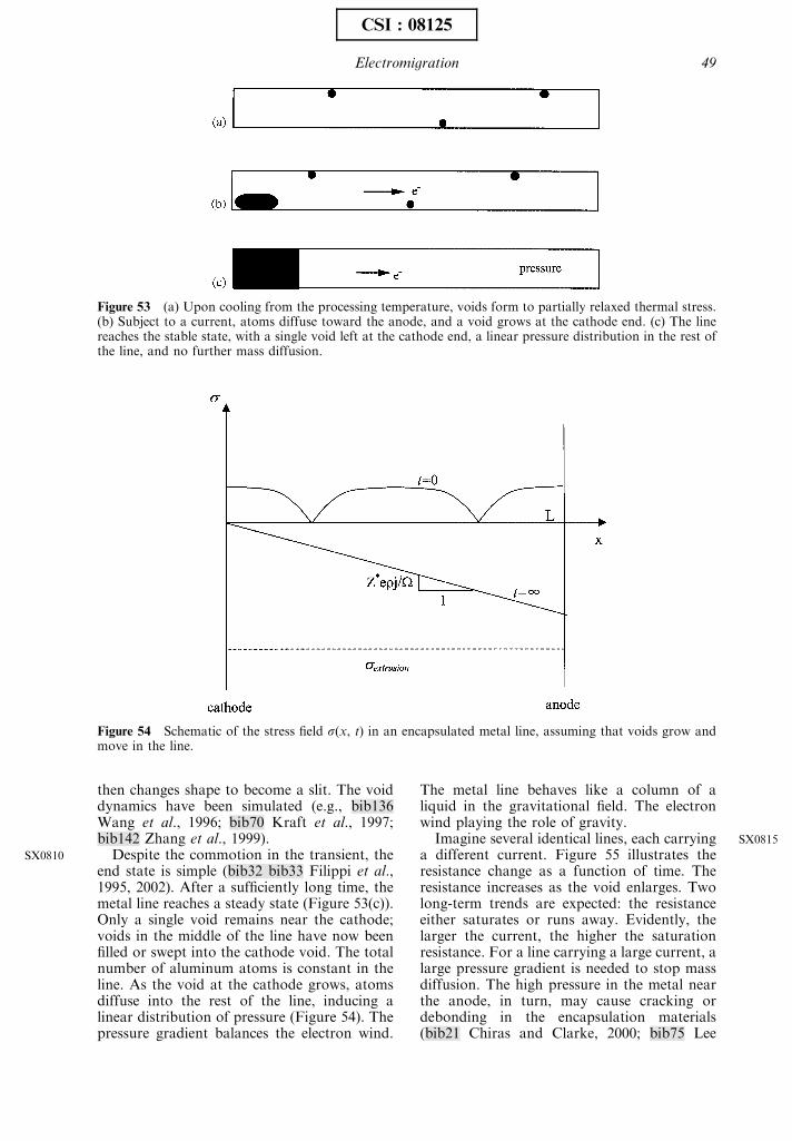
then changes shape to become a slit. The voiddynamics have been simulated (e.g., bib136Wang et al., 1996; bib70 Kraft et al., 1997;bib142 Zhang et al., 1999).
Despite the commotion in the transient, theend state is simple (bib32 bib33 Filippi et al.,1995, 2002). After a sufficiently long time, themetal line reaches a steady state (Figure 53(c)).Only a single void remains near the cathode;voids in the middle of the line have now beenfilled or swept into the cathode void. The totalnumber of aluminum atoms is constant in theline. As the void at the cathode grows, atomsdiffuse into the rest of the line, inducing alinear distribution of pressure (Figure 54). Thepressure gradient balances the electron wind.
The metal line behaves like a column of aliquid in the gravitational field. The electronwind playing the role of gravity.
Imagine several identical lines, each carryinga different current. Figure 55 illustrates theresistance change as a function of time. Theresistance increases as the void enlarges. Twolong-term trends are expected: the resistanceeither saturates or runs away. Evidently, thelarger the current, the higher the saturationresistance. For a line carrying a large current, alarge pressure gradient is needed to stop massdiffusion. The high pressure in the metal nearthe anode, in turn, may cause cracking ordebonding in the encapsulation materials(bib21 Chiras and Clarke, 2000; bib75 Lee
Figure 53 (a) Upon cooling from the processing temperature, voids form to partially relaxed thermal stress.(b) Subject to a current, atoms diffuse toward the anode, and a void grows at the cathode end. (c) The linereaches the stable state, with a single void left at the cathode end, a linear pressure distribution in the rest ofthe line, and no further mass diffusion.
Figure 54 Schematic of the stress field s(x, t) in an encapsulated metal line, assuming that voids grow andmove in the line.
SX0810
SX0815
Electromigration 49
CSI : 08125
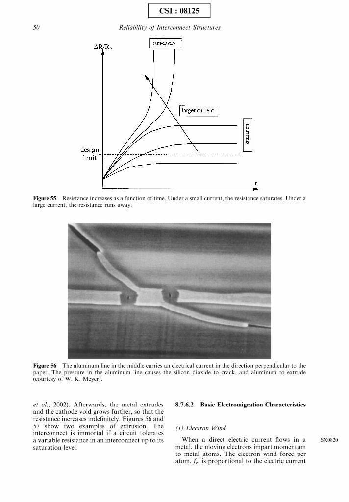
et al., 2002). Afterwards, the metal extrudesand the cathode void grows further, so that theresistance increases indefinitely. Figures 56 and57 show two examples of extrusion. Theinterconnect is immortal if a circuit toleratesa variable resistance in an interconnect up to itssaturation level.
8.7.6.2 Basic Electromigration Characteristics
(i) Electron Wind
When a direct electric current flows in ametal, the moving electrons impart momentumto metal atoms. The electron wind force peratom, fe, is proportional to the electric current
Figure 55 Resistance increases as a function of time. Under a small current, the resistance saturates. Under alarge current, the resistance runs away.
Figure 56 The aluminum line in the middle carries an electrical current in the direction perpendicular to thepaper. The pressure in the aluminum line causes the silicon dioxide to crack, and aluminum to extrude(courtesy of W. K. Meyer).
SX0820
50 Reliability of Interconnect Structures
CSI : 08125
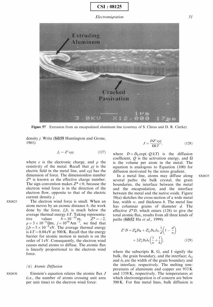
density j. Write (bib59 Huntington and Grone,1961)
fe ¼ Z�erj; ð127Þ
where e is the electronic charge, and r theresistivity of the metal. Recall that rj is theelectric field in the metal line, and erj has thedimension of force. The dimensionless numberZ* is known as the effective charge number.The sign convention makes Z*o0, because theelectron wind force is in the direction of theelectron flow, opposite to that of the electriccurrent density j.
The electron wind force is small. When anatom moves by an atomic distance b, the workdone by the force, feb, is much below theaverage thermal energy kT. Taking representa-tive values b¼ 10�10m, Z*¼�2,r¼ 3� 10�8Om, j¼ 1010Am�2, we find thatfeb¼ 5� 10�8 eV. The average thermal energyis kT¼ 0.04 eV at 500K. Recall that the energybarrier for atomic motion in metals is on theorder of 1 eV. Consequently, the electron windcauses metal atoms to diffuse. The atomic fluxis linearly proportional to the electron windforce.
(ii) Atomic Diffusion
Einstein’s equation relates the atomic flux J(i.e., the number of atoms crossing unit areaper unit time) to the electron wind force:
J ¼ DZ�erj
OkT; ð128Þ
where D¼D0 exp(–Q/kT) is the diffusioncoefficient, Q is the activation energy, and Ois the volume per atom in the metal. Theequation is analogous to Equation (100) fordiffusion motivated by the stress gradient.
In a metal line, atoms may diffuse alongseveral paths: the bulk crystal, the grainboundaries, the interface between the metaland the encapsulation, and the interfacebetween the metal and the native oxide. Figure58(a) sketches the cross-section of a wide metalline, width w, and thickness h. The metal linehas columnar grains of diameter d. Theeffective Z*D, which enters (128) to give thetotal atomic flux, results from all three kinds ofpaths (bib52 Hu et al., 1999):
Z�D ¼Z�BDB þ Z�
GDGdG1
d1� d
w
� �
þ 2Z�I DIdI
1
wþ 1
h
� �; ð129Þ
where the subscripts B, G, and I signify thebulk, the grain boundary, and the interface; dGand dI are the width of the grain boundary andthe interface, respectively. The melting tem-peratures of aluminum and copper are 933Kand 1358K, respectively. The temperatures atwhich electromigration is of concern are below500K. For fine metal lines, bulk diffusion is
Figure 57 Extrusion from an encapsulated aluminum line (courtesy of S. Chiras and D. R. Clarke).
SX0825
SX0830
SX0835
Electromigration 51
CSI : 08125
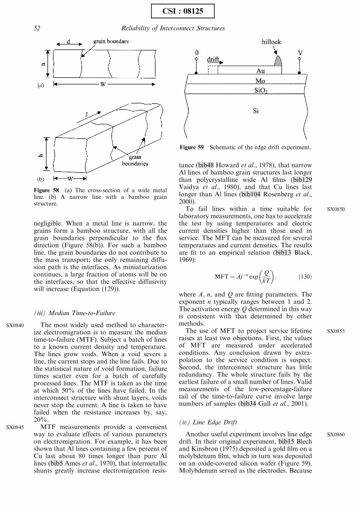
negligible. When a metal line is narrow, thegrains form a bamboo structure, with all thegrain boundaries perpendicular to the fluxdirection (Figure 58(b)). For such a bambooline, the grain boundaries do not contribute tothe mass transport; the only remaining diffu-sion path is the interfaces. As miniaturizationcontinues, a large fraction of atoms will be onthe interfaces, so that the effective diffusivitywill increase (Equation (129)).
(iii) Median Time-to-Failure
The most widely used method to character-ize electromigration is to measure the mediantime-to-failure (MTF). Subject a batch of linesto a known current density and temperature.The lines grow voids. When a void severs aline, the current stops and the line fails. Due tothe statistical nature of void formation, failuretimes scatter even for a batch of carefullyprocessed lines. The MTF is taken as the timeat which 50% of the lines have failed. In theinterconnect structure with shunt layers, voidsnever stop the current. A line is taken to havefailed when the resistance increases by, say,20%.
MTF measurements provide a convenientway to evaluate effects of various parameterson electromigration. For example, it has beenshown that Al lines containing a few percent ofCu last about 80 times longer than pure Allines (bib5 Ames et al., 1970), that intermetallicshunts greatly increase electromigration resis-
tance (bib48 Howard et al., 1978), that narrowAl lines of bamboo grain structures last longerthan polycrystalline wide Al films (bib129Vaidya et al., 1980), and that Cu lines lastlonger than Al lines (bib104 Rosenberg et al.,2000).
To fail lines within a time suitable forlaboratory measurements, one has to acceleratethe test by using temperatures and electriccurrent densities higher than those used inservice. The MFT can be measured for severaltemperatures and current densities. The resultsare fit to an empirical relation (bib13 Black,1969):
MFT ¼ Aj�n expQ
kT
� �; ð130Þ
where A, n, and Q are fitting parameters. Theexponent n typically ranges between 1 and 2.The activation energy Q determined in this wayis consistent with that determined by othermethods.
The use of MFT to project service lifetimeraises at least two objections. First, the valuesof MFT are measured under acceleratedconditions. Any conclusion drawn by extra-polation to the service condition is suspect.Second, the interconnect structure has littleredundancy. The whole structure fails by theearliest failure of a small number of lines. Validmeasurements of the low-percentage-failuretail of the time-to-failure curve involve largenumbers of samples (bib34 Gall et al., 2001).
(iv) Line Edge Drift
Another useful experiment involves line edgedrift. In their original experiment, bib15 Blechand Kinsbron (1975) deposited a gold film on amolybdenum film, which in turn was depositedon an oxide-covered silicon wafer (Figure 59).Molybdenum served as the electrodes. Because
Figure 58 (a) The cross-section of a wide metalline. (b) A narrow line with a bamboo grainstructure.
Figure 59 Schematic of the edge drift experiment.
SX0840
SX0845
SX0850
SX0855
SX0860
52 Reliability of Interconnect Structures
CSI : 08125
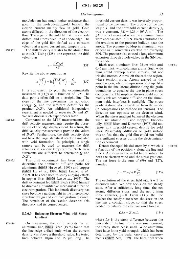
molybdenum has much higher resistance thangold, in the molybdenum/gold bilayer, theelectric current mainly flew in gold. Goldatoms diffused in the direction of the electronflow. The edge of the gold film at the cathodedrifted, and atoms piled up at anode edge. Theedge of the gold film drifted at a constantvelocity at a given current and temperature.
The drift velocity v relates to the atomic fluxas v¼OJ. Using (128), one expresses the driftvelocity as
v ¼ DZ�erj
kT: ð131Þ
Rewrite the above equation as
lnvT
j
� �¼ ln
D0Z�erk
� �� Q
kT: ð132Þ
It is convenient to plot the experimentallymeasured ln (vT/j) as a function of 1/T. Thedata points often fall on a straight line. Theslope of the line determines the activationenergy Q, and the intercept determines theproduct D0Z*. An additional independentexperiment is needed to separate D0 and Z*.We will discuss such experiments later.
Compared to the MTF measurements, thedrift velocity measurements require the obser-vation of the edge displacement. In return, thedrift velocity measurements provide the valuesof D0Z*. Furthermore, the drift velocity doesnot have the large statistical scatter associatedwith void formation. In principle, a singlesample can be used to measure the driftvelocities at various temperatures. Such mea-surements are sufficient to determine Q andD0Z*.
The drift experiment has been used todetermine the dominant diffusion paths foraluminum (bib53 Hu et al., 1993) and copper(bib52 Hu et al., 1999; bib81 Liniger et al.,2002). It has been used to study alloying effectsin copper lines (bib76 Lee et al., 1995). Thedrift experiment led bib14 Blech (1976) himselfto discover a quantitative mechanical effect onelectromigration. This landmark discovery hassince become a guiding light in the interconnectstructure design and electromigration research.The remainder of the section describes thisdiscovery and its consequences.
8.7.6.3 Balancing Electron Wind with StressGradient
On measuring the drift velocity in analuminum line, bib14 Blech (1976) found thatthe line edge drifted only when the currentdensity was above a threshold value. He testedlines between 30 mm and 150 mm long. The
threshold current density was inversely propor-tional to the line length. The product of the linelength L and the threshold current density jcwas a constant, jcL ¼ 1:26� 105 A m�1: ThejcL product increased when the aluminum lineswere encapsulated in SiN. Blech attributed theobservations to the pressure buildup near theanode. The pressure buildup in aluminum wasevident as it sometimes cracked the overlyingSiN. The pressure also caused a long aluminumextrusion through a hole etched in the SiN nearthe anode.
Blech used aluminum lines 25 mm wide and0.46 mm thick, with columnar grains. Such widefilms could develop biaxial stresses, but nottriaxial stresses. Atoms left the cathode region,where tension arose. Atoms arrived in theanode region, where compression built up. At apoint in the line, atoms diffuse along the grainboundaries to equalize the two in-plane stresscomponents. The in-plane stresses could not bereadily relaxed because diffusion on the alumi-num–oxide interfaces is negligible. The stressgradient drove atoms to diffuse from the anode(in compression) to cathode (in tension). Thedirection was opposite to the electron wind.When the stress gradient balanced the electronwind, net atomic diffusion stopped. Inciden-tally, bib15 Blech and Kinsbron (1975) did notreport any threshold current density for goldlines. Presumably, diffusion on gold surfacewas so fast that the gold film could not buildup significant stresses during the electromigra-tion experiment.
Denote the equal biaxial stress by s, which isa function of the position x along the line andtime t. An atom in the metal line is subject toboth the electron wind and the stress gradient.The net force is the sum of (99) and (127),namely,
f ¼ Z�erj þ Oqsqx
: ð133Þ
The evolution of the stress field s(x, t) will bediscussed later. We now focus on the steadystate. After a sufficiently long time, the netatomic diffusion stops, and the net drivingforce vanishes, f¼ 0. From (133), the linereaches the steady state when the stress in theline has a constant slope, so that the stressneeded to balance the electron wind force is
ODs ¼ Z�erjL; ð134Þ
where Ds is the stress difference between thetwo ends of the line. For a very small current,the steady stress Ds is small. Wide aluminumlines have finite yield strength, which has beendetermined by the wafer curvature measure-ments (bib95 Nix, 1989). The lines drift when
SX0865
SX0870
SX0875
SX0880
SX0885
SX0890
Electromigration 53
CSI : 08125
the stresses at both ends exceed the yieldstrength. Take O¼ 1.66� 10�29m3, Z*¼�2,r¼ 3� 10�8Om, Ds¼ 108 Pa, and we find thatjcL¼ 1.73� 105Am�1.
The mechanical constraint effect on electro-migration lifetime had been reported beforeBlech’s work. For example, bib1 Ainslie et al.(1972) developed Equation (134) to estimatethe stress needed to stop electromigration.These authors used a value Z*¼�60 in theirestimate, and found an extremely large stress,which could not be sustained by the encapsula-tion. They abandoned this interpretation, andinstead tried to explain the mechanical effect interms of the effect of stress on diffusivity. TheBlech experiment eliminated any diffusivity-related interpretation, because diffusionstopped when the current was below thethreshold. Indeed, once the threshold currentis measured, together with the yield strengthmeasured by the wafer curvature method,Equation (134) determines the value of Z*,without being convoluted with the diffusivity.
8.7.6.4 No-Voiding Condition forEncapsulated Line
We now return to Figure 52 for a quantita-tive discussion. On cooling from the stress-freetemperature T0 to a temperature T, the metalline and the encapsulation have a mismatchvolumetric strain 3Da(T0�T). When the struc-ture is held at T for a sufficiently long time, theline will evolve into one of the two equilibriumstates: either a uniform hydrostatic stress states¼ 3Da(T0�T)B with no voids, or a stress-freestate with a saturated void volume,SVV¼ 3Da(T0�T)V. Here V is the volume ofthe metal line. Section 8.7.5.6 prescribes waysto calculate the effective thermal expansioncoefficient mismatch Da and elastic modulus B.The evolution is facilitated by atomic trans-port. At a finite time, the metal line is in atransient state. The stress state is nonhydro-static and nonuniform. Voids and unrelaxedmetal coexist.
Of the two equilibrium states, the hydro-static state is metastable, but the state withSVV is stable. Consider the hydrostatic statefirst. In Figure 52, this hydrostatic stress field islabeled as t¼ 0. Section 8.7.5.2 prescribes acritical stress for void initiation, svoid¼ 2g/a,where a is the radius of the pre-existing flawsize, and g the surface energy. The conditioncan be modified for flaws on interfaces, orjunctions between the grain boundaries and theinterfaces. It is assumed that the annealing willclose all voids provided the uniform hydro-static stress is below the critical stress, sosvoid.
For a copper/low-k structure, takingDa¼ 13� 10�6K�1, T0�T¼ 200K,B¼ 6� 109 Pa, g¼ 1 Jm�2 and a¼ 5 nm, wefind that the hydrostatic stress iss¼ 0.47� 108 Pa, and the critical stress issvoid¼ 4� 108 Pa. This comparison seems tosuggest that the compliant dielectrics reduce B,making the stress-induced voiding less likely.
The above void initiation condition is overlysimplistic, and is risky. It assumes an artificialscenario: the metal reaches the hydrostaticstate first, and then the flaws start to questionthemselves whether to enlarge or shrink. Inreality, during annealing, the elastic anisotropybetween metal grains, as well as the elasticinhomogeneity between the metal and theencapsulation, can momentarily cause veryhigh stresses at various junctions. If atomictransport is slow in relaxing the metal into thehydrostatic state, the high stresses may causethe flaws to grow. The situation is worse thanvoiding in blanket films discussed in Section8.7.5.4. A stress-free and void-free blanket filmis the stable equilibrium state. By contrast, inan encapsulated metal line, the uniform hydro-static state is only metastable; the voids, onceinitiated, will grow until the entire line is stressfree. Experiments of bib41 Hau-Riege (2001)showed that voids formed in copper lines evenat very small electric current.
With caution, we pursue this risky modelfurther, asking whether a superimposed electriccurrent will initiate voiding. After the electriccurrent is applied, the metal line evolves to asteady state, in which the stress is linearlydistributed. The number of atoms is conservedin the metal line. If no voids form, atoms lost inthe cathode region relocate to the anoderegion. By symmetry, the middle of the lineneither loses nor gains atoms, and remains tohave the stress, s(L/2, t)¼ 3Da(T0�T)B, at alltime. The steady stress state as t-N in the lineis
sðx;NÞ ¼ 3DaðT0 � TÞB � Z�erj
Ox � L
2
� �: ð136Þ
In Figure 52, this steady state stress field islabeled as t¼N.
We assume that voids do not initiate if thesteady stress at the cathode is below the criticalstress, s(0,N)osvoid, namely,
3DaðT0 � TÞB þ Z�er2O
jLosvoid: ð137Þ
Figure 60 sketches this condition on the planespanned by the temperature T and the productjL. On this plane, Equation (137) is the straightline. Below the straight line, the current densityis low and the temperature is high, so voids will
SX0895
SX0900
SX0905
SX0910
SX0915
SX0920
54 Reliability of Interconnect Structures
CSI : 08125
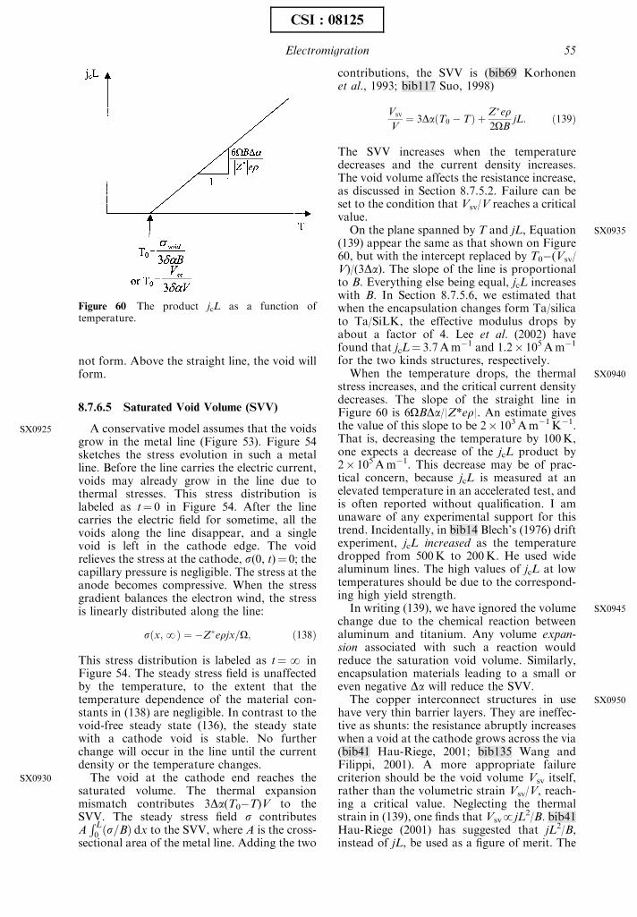
not form. Above the straight line, the void willform.
8.7.6.5 Saturated Void Volume (SVV)
A conservative model assumes that the voidsgrow in the metal line (Figure 53). Figure 54sketches the stress evolution in such a metalline. Before the line carries the electric current,voids may already grow in the line due tothermal stresses. This stress distribution islabeled as t¼ 0 in Figure 54. After the linecarries the electric field for sometime, all thevoids along the line disappear, and a singlevoid is left in the cathode edge. The voidrelieves the stress at the cathode, s(0, t)¼ 0; thecapillary pressure is negligible. The stress at theanode becomes compressive. When the stressgradient balances the electron wind, the stressis linearly distributed along the line:
sðx;NÞ ¼ �Z�erjx=O; ð138Þ
This stress distribution is labeled as t¼N inFigure 54. The steady stress field is unaffectedby the temperature, to the extent that thetemperature dependence of the material con-stants in (138) are negligible. In contrast to thevoid-free steady state (136), the steady statewith a cathode void is stable. No furtherchange will occur in the line until the currentdensity or the temperature changes.
The void at the cathode end reaches thesaturated volume. The thermal expansionmismatch contributes 3Da(T0�T)V to theSVV. The steady stress field s contributesAR L
0 ðs=BÞ dx to the SVV, where A is the cross-sectional area of the metal line. Adding the two
contributions, the SVV is (bib69 Korhonenet al., 1993; bib117 Suo, 1998)
Vsv
V¼ 3DaðT0 � TÞ þ Z�er
2OBjL: ð139Þ
The SVV increases when the temperaturedecreases and the current density increases.The void volume affects the resistance increase,as discussed in Section 8.7.5.2. Failure can beset to the condition that Vsv/V reaches a criticalvalue.
On the plane spanned by T and jL, Equation(139) appear the same as that shown on Figure60, but with the intercept replaced by T0�(Vsv/V)/(3Da). The slope of the line is proportionalto B. Everything else being equal, jcL increaseswith B. In Section 8.7.5.6, we estimated thatwhen the encapsulation changes form Ta/silicato Ta/SiLK, the effective modulus drops byabout a factor of 4. Lee et al. (2002) havefound that jcL¼ 3.7Am�1 and 1.2� 105Am�1
for the two kinds structures, respectively.When the temperature drops, the thermal
stress increases, and the critical current densitydecreases. The slope of the straight line inFigure 60 is 6OBDa/|Z*er|. An estimate givesthe value of this slope to be 2� 103Am�1K�1.That is, decreasing the temperature by 100K,one expects a decrease of the jcL product by2� 105Am�1. This decrease may be of prac-tical concern, because jcL is measured at anelevated temperature in an accelerated test, andis often reported without qualification. I amunaware of any experimental support for thistrend. Incidentally, in bib14 Blech’s (1976) driftexperiment, jcL increased as the temperaturedropped from 500K to 200K. He used widealuminum lines. The high values of jcL at lowtemperatures should be due to the correspond-ing high yield strength.
In writing (139), we have ignored the volumechange due to the chemical reaction betweenaluminum and titanium. Any volume expan-sion associated with such a reaction wouldreduce the saturation void volume. Similarly,encapsulation materials leading to a small oreven negative Da will reduce the SVV.
The copper interconnect structures in usehave very thin barrier layers. They are ineffec-tive as shunts: the resistance abruptly increaseswhen a void at the cathode grows across the via(bib41 Hau-Riege, 2001; bib135 Wang andFilippi, 2001). A more appropriate failurecriterion should be the void volume Vsv itself,rather than the volumetric strain Vsv/V, reach-ing a critical value. Neglecting the thermalstrain in (139), one finds that VsvpjL2/B. bib41Hau-Riege (2001) has suggested that jL2/B,instead of jL, be used as a figure of merit. The
Figure 60 The product jcL as a function oftemperature.
SX0925
SX0930
SX0935
SX0940
SX0945
SX0950
Electromigration 55
CSI : 08125
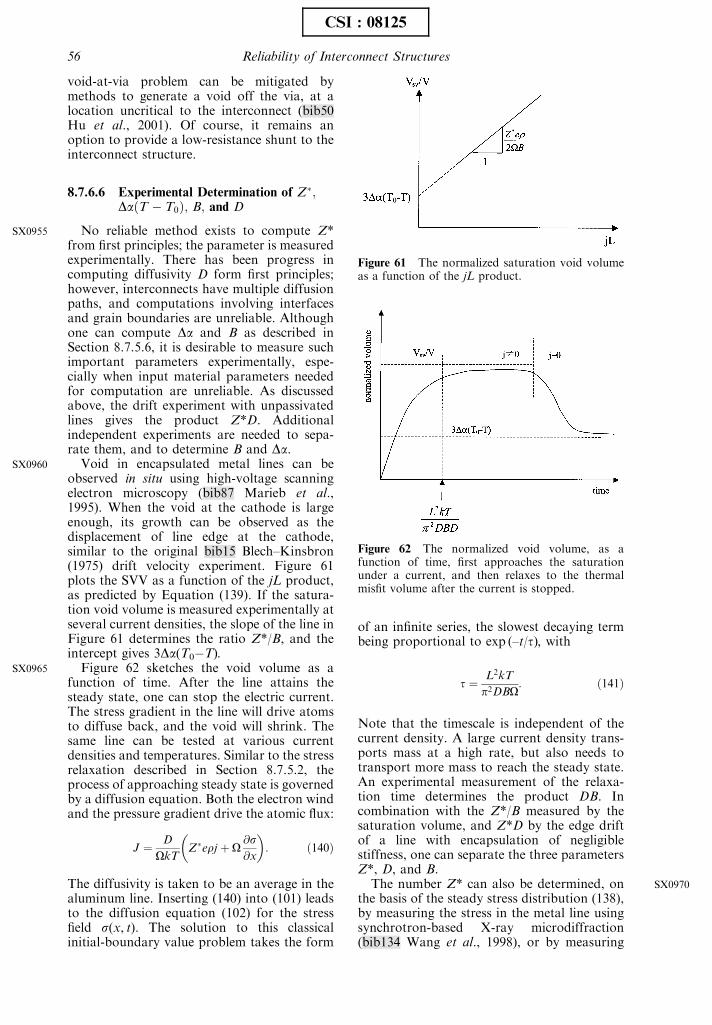
void-at-via problem can be mitigated bymethods to generate a void off the via, at alocation uncritical to the interconnect (bib50Hu et al., 2001). Of course, it remains anoption to provide a low-resistance shunt to theinterconnect structure.
8.7.6.6 Experimental Determination of Z�;DaðT � T0Þ; B; and D
No reliable method exists to compute Z*from first principles; the parameter is measuredexperimentally. There has been progress incomputing diffusivity D form first principles;however, interconnects have multiple diffusionpaths, and computations involving interfacesand grain boundaries are unreliable. Althoughone can compute Da and B as described inSection 8.7.5.6, it is desirable to measure suchimportant parameters experimentally, espe-cially when input material parameters neededfor computation are unreliable. As discussedabove, the drift experiment with unpassivatedlines gives the product Z*D. Additionalindependent experiments are needed to sepa-rate them, and to determine B and Da.
Void in encapsulated metal lines can beobserved in situ using high-voltage scanningelectron microscopy (bib87 Marieb et al.,1995). When the void at the cathode is largeenough, its growth can be observed as thedisplacement of line edge at the cathode,similar to the original bib15 Blech–Kinsbron(1975) drift velocity experiment. Figure 61plots the SVV as a function of the jL product,as predicted by Equation (139). If the satura-tion void volume is measured experimentally atseveral current densities, the slope of the line inFigure 61 determines the ratio Z*/B, and theintercept gives 3Da(T0�T).
Figure 62 sketches the void volume as afunction of time. After the line attains thesteady state, one can stop the electric current.The stress gradient in the line will drive atomsto diffuse back, and the void will shrink. Thesame line can be tested at various currentdensities and temperatures. Similar to the stressrelaxation described in Section 8.7.5.2, theprocess of approaching steady state is governedby a diffusion equation. Both the electron windand the pressure gradient drive the atomic flux:
J ¼ D
OkTZ�erj þ O
@s@x
� �: ð140Þ
The diffusivity is taken to be an average in thealuminum line. Inserting (140) into (101) leadsto the diffusion equation (102) for the stressfield s(x, t). The solution to this classicalinitial-boundary value problem takes the form
of an infinite series, the slowest decaying termbeing proportional to exp (–t/t), with
t ¼ L2kT
p2DBO: ð141Þ
Note that the timescale is independent of thecurrent density. A large current density trans-ports mass at a high rate, but also needs totransport more mass to reach the steady state.An experimental measurement of the relaxa-tion time determines the product DB. Incombination with the Z*/B measured by thesaturation volume, and Z*D by the edge driftof a line with encapsulation of negligiblestiffness, one can separate the three parametersZ*, D, and B.
The number Z* can also be determined, onthe basis of the steady stress distribution (138),by measuring the stress in the metal line usingsynchrotron-based X-ray microdiffraction(bib134 Wang et al., 1998), or by measuring
Figure 62 The normalized void volume, as afunction of time, first approaches the saturationunder a current, and then relaxes to the thermalmisfit volume after the current is stopped.
Figure 61 The normalized saturation void volumeas a function of the jL product.
SX0955
SX0960
SX0965
SX0970
56 Reliability of Interconnect Structures
CSI : 08125
the fringe stress field in silicon using Ramanspectroscopy (bib84 Ma et al., 1995).
8.7.6.7 No-Extrusion Condition forEncapsulated Line
In the steady state with SVV, the compres-sive stress in the metal line at the anode is
sA ¼ �Z�erjL=O: ð142Þ
Using L¼ 100 mm, j¼ 1.0� 1010Am�2, Z*¼ 2,e¼ 1.6� 10�19 C, r¼ 3� 108Om, andO¼ 1.66� 10–29m3, one finds that the steady-state compressive stress at the anode issA¼�600MPa. The large stress may causecracking or debonding of the encapsulation.For example, bib32 Filippi et al. (1995) tested100 mm aluminum lines under various currentdensities, and reported that aluminum did notextrude under 0.56� 1010Am�2, but did under1.0� 1010Am�2.
Section 8.7.2.2 has outlined the applicationof fracture mechanics to structures of smallfeature size. The fabrication process controlsthe geometry all the way to the feature size, sothat crack-like flaws must be smaller than thefeature size. Use the linewidth, w, as arepresentative size scale, the no-extrusion con-dition is stated as (bib117 Suo, 1998)
bs2Aw
EoG; ð143Þ
Here G is the fracture energy of the encapsula-tion material or the interface, E the Young’smodulus of the material, and b a dimensionlessparameter depending on ratios of variouselastic moduli and lengths that describe theanode. The values of b can be calculated bysolving the elasticity boundary value problemscontaining cracks. Taking representative valuessuch as b¼ 0.25, G¼ 4 Jm�2, E¼ 70GPa, andw¼ 0.5 mm, one finds from (2) that the en-capsulation can sustain anode pressure up to|sA|¼ 1.5GPa.
In the above, thermal stresses in the passiva-tion have been ignored. Upon cooling from theprocessing temperature, a large compressivehoop stress arises in the oxide, resulting fromthe thermal expansion misfits between thealuminum and the oxide, and between thesilicon substrate and the oxide. When anelectric current is supplied, the volume ofaluminum near the anode increases, which firstcompensates its thermal contraction, and thengoes beyond. Consequently, in the stable state,the stress in the oxide is due to the pressure inthe aluminum, and the thermal misfit between
the oxide and the silicon substrate. The latter isnegligible.
Two other circumstances should be men-tioned in this connection. Some dielectrics maydevelop large intrinsic stresses at the depositiontemperature. They are unrelated to the volumechange of aluminum, and persist under tem-perature change and current. A second circum-stance involves a line tested under a current upto the stable state, and then brought to a highertemperature. Instantaneously, the thermal ex-pansion misfit between aluminum and oxideadds more tensile stress in the insulator. Insuch cases, the additional stresses must beincluded in the no-extrusion condition.
Compliant low-k dielectrics present a newchallenge. As a first approximation, we modelthe Ta barrier as a cylindrical pressure vessel ofradius a and thickness hb, and neglect thedielectric. The hoop stress in the barrier syrelates to the internal pressure sA as sy¼ |sA|a/hb. Assume that crack-like flaw size is on theorder of the barrier thickness hb. The no-extrusion condition may be written as
bs2Aa2
EhboG: ð144Þ
The above estimates are intended to illus-trate a basic modeling approach. Because thestructural details at line ends are complicated,accurate calculation is difficult. A more reliablemethod is to carry out experiments with knowncurrent density, and use the electromigrationgenerated stress to test the condition forextrusion (bib21 Chiras and Clarke, 2000).
8.7.6.8 The Immortal Interconnect
Provided a circuit tolerates a variableresistance in an interconnect up to its satura-tion level, the interconnect is immortal (bib117Suo, 1998; bib6 Andleigh et al., 1999). Theinterconnect evolves into a stable state to adaptto the newly established temperature andcurrent. The immortality gives a simple per-spective on reliability. One can focus on thestable state itself, rather than the transientprocess to reach it. The perspective plays downthe roles of the timescale, the rate processes,and the microstructure of the metal. No longerneed the microstructure be optimized for slowmass transport or low void nucleation rate. Nolonger need the MTF be measured, for thelifetime is infinite. No longer need a magicalloy be sought to slow down diffusion rate, forthe diffusivity is irrelevant. In short, thereliability is warranted by energetics, rather
SX0975
SX0980
SX0985
SX0990
SX0995
SX1000
SX1005
Electromigration 57
CSI : 08125
than kinetics. Having thermodynamics on ourside, the design is much more robust.
The use of the stable state is limited in twoways: the metal may extrude at the anode, orthe saturation resistance may be prohibitivelylarge. For a short line, the saturation voidvolume is small compared to the via size, givingrise to a small change in resistance. Conse-quently, the stable state finds ready applica-tions in short lines. The saturation void volumeincreases when the effective modulus B is small(Equation (139)). The interconnect structurewith low-k dielectrics and thin barriers nodoubt require attention. The copper intercon-nect structures in use have very thin barrierlayers. They are ineffective as shunts: theresistance abruptly increases when a void atthe cathode grows across the via. An immortalinterconnect would require low-resistanceshunts.
As miniaturization continues, larger fractionof atoms will be on the metal/encapsulationinterface. The effective diffusivity will be larger(Equation (129)), and the diffusion time short-er. The day may arrive when some of theinterconnects must be designed to be immortal.Investigation into ways to limit the resistanceincrease and to prevent metal extrusion willprepare us for such a day.
ACKNOWLEDGMENTS
The work of my group in this area has beensupported over the years by the NationalScience Foundation, Office of Navel Research,Defense Advanced Research Projects Agency,New Jersey Science and Technology Commis-sion, Institute for Materials Research andEngineering, and Intel Corporation. Dr. Z. Y.Huang has kindly helped me prepare thefigures.
REFERENCES
N. G. Ainslie, F. M. d’Heurle and O. C. Wells, 1972,Coating, mechanical constraints, and pressure effects onelectromigration. Appl. Phys. Lett., 20, 173–174.
P. Alpern, V. Wicher and R. Tilgner, 1994, A simple testchip to assess chip and package design in the case ofplastic assembling. IEEE Trans. Compon. Pack. Manuf.Technol. A, 17, 583–589 (correction in 1995, 18, 862–863).
J. M. Ambrico and M. R. Begley, 2002, The role of initialflaw size and plasticity in adjacent layers in channelingcrack growth in thin films, submitted.
J. M. Ambrico, E. E. Jones and M. R. Begley, 2002,Cracking in thin multi-layers with finite width andperiodic architectures. Int. J. Solids Struct., 39, 1443–1462.
I. Ames, F. d’Heurle and R. Horstmann, 1970, Reductionof electromigration in aluminum films by copper doping.IBM J. Res. Develop., 14, 461–463.
V. K. Andleigh, V. T. Srikar, Y. J. Park and C. V.Thompson, 1999, Mechanism maps for electromigra-tion-induced failure of metal and alloy interconnects. J.Appl. Phys., 86, 6737–6745.
E. Arzt, O. Kraft, W. D. Nix and J. E. Sanchez, 1994,Electromigration failure by shape change of voids inbamboo lines. J. Appl. Phys., 76, 1563–1571.
A. Bagchi, G. E. Lucus, Z. Suo and A. G. Evans, 1994, Anew procedure for measuring the decohesion energy forthin ductile films on substrate. J. Mater. Res., 9, 1734–1741.
S. P. Baker, A. Kretschmann and E. Arzt, 2001, Thermo-mechanical behavior of different texture components inCu thin films. Acta Mater., 49, 2145–2160.
M. R. Begley and A. G. Evans, 2001, Progressive crackingof a multilayer system upon thermal cycling. J. Appl.Mech., 68, 513–520.
J. L. Beuth, 1992, Cracking of thin bonded films in residualtension. Int. J. Solids Struct., 29, 1657–1675.
J. L. Beuth and N. W. Klingbeil, 1996, Cracking of thinfilms bonded to elastic–plastic substrates. J. Mech. Phys.Solids, 44, 1411–1428.
J. R. Black, 1969, Electromigration—a brief survey andsome recent results. IEEE Trans. Electron Devices, ED-
16, 338–347.I. A. Blech, 1976, Electromigration in thin aluminum filmson titanium nitride. J. Appl. Phys., 47, 1203–1208.
I. A. Blech and E. Kinsbron, 1975, Electromigration in thingold films on molybdenum surfaces. Thin Solid Films, 25,327–334.
I. A. Blech and E. S. Meieran, 1967, Direct transmissionelectron microscope observation of electrotransport inaluminum thin films. Appl. Phys. Lett., 11, 263–265.
J. Bree, 1967, Elastic–plastic behaviour of thin tubessubjected to internal pressure and intermittent high-heatfluxes with application to fast-nuclear-reactor fuelelements. J. Strain Analysis, 2, 226–238.
B. Budiansky, J. W. Hutchinson and S. Slutsky, 1982, Voidgrowth and collapse in viscous solids. In: ‘‘Mechanics ofSolids, The Rodney Hill 60th Anniversary Volume,’’ eds.H. G. Hopkins and J. Sewell, Pergamon Press, Oxford,pp. 13–45.
H. C. Cao and A. G. Evans, 1989, An experimental studyof the fracture resistance of bimaterial interface. Mech.Mater., 7, 295–305.
P. G. Charalambides, J. Lund, A. G. Evans and R. M.McMeeking, 1989, A test specimen for determining thefracture resistance of bimaterial interfaces. J. Appl.Mech., 56, 77–82.
S. Chiras and D. R. Clarke, 2000, Dielectric crackingproduced by electromigration in microelectronic inter-connects. J. Appl. Phys., 88, 6302–6312.
T.-J. Chuang, K. I. Kagawa, J. R. Rice and L. B. Sills,1979, Non-equilibrium models for diffusive cavitation ofgrain interfaces. Acta Metall., 27, 265–284.
R. F. Cook and E. G. Liniger, 1999, Stress-corrosioncracking of low-dielectric-constant spin-on-glass thinfilms. J. Electochem. Soc., 146, 4439–4448.
J. Curry, G. Fitzgibbon, Y. Guan, R. Muollo, G. Nelsonand A. Thomas, 1984, New failure mechanisms insputtered aluminum–silicon films. In: ‘‘22nd Ann. Proc.IEEE Int. Reliability Phys. Symp.,’’ pp. 6–8.
R. H. Dauskardt, M. Lane, Q. Ma and N. Krishna, 1998,Adhesion and debonding of multi-layer thin filmstructures. Eng. Fract. Mech., 61, 141–162.
F. M. d’Heurle and P. S. Ho, 1978, Electromigration inthin films. In: ‘‘Thin Films: Interdiffusion and Reac-tions,’’ eds. J. Poate, K. N. Tu and J. Mayer, Wiley, NewYork, pp. 243–303.
F. M. d’Heurle and R. Rosenberg, 1973, Electromigrationin thin films. In: ‘‘Physics of Thin Films,’’ eds. G. Hass,M. Francombe and R. Hoffman, Academic Press, NewYork, vol. 7, pp. 257–310.
SX1010
SX1015
SX1016
bib1
bib2
bib3
AU:8
bib4
bib5
bib6
bib7
bib8
bib9
bib10
bib11
bib12
bib13
bib14
bib15
bib16
bib17
bib18
bib19
bib20
bib21
bib22
bib23
bib24
AU:9
bib25
bib26
bib27
58 Reliability of Interconnect Structures
CSI : 08125
D. R. Edwards, K. G. Heinen, S. K. Groothuis and J. E.Martinez, 1987, Shear-stress evaluation of plasticpackages. IEEE Trans. Compon. Hybrids Manuf. Tech-nol., 12, 618–627.
F. Erdogan and G. C. Sih, 1963, On the crack extension inplates under plane loading and transverse shear. J. BasicEng., Trans. ASME, 85, 519–527.
A. G. Evans, M. D. Drory and M. S. Hu, 1988, Thecracking and decohesion of thin films. J. Mater. Res., 3,1043–1049.
A. G. Evans and J. W. Hutchinson, 1995, The thermo-mechanical integrity of thin films and multilayers. ActaMetall. Mater., 43, 2507–2530.
R. G. Filippi, G. A. Biery and R. A. Wachnik, 1995, Theelectromigration short-length effect in Ti–AlCu–Timetallization with tungsten studs. J. Appl. Phys., 78,3756–3768.
R. G. Filippi, R. A. Wachnik, C.-P. Eng, D. Chidambar-rao, P.-C. Wang, J. F. White, M. A. Korhonen, T. M.Shaw, R. Rosenberg and T. D. Sullivan, 2002, The effectof current density, stripe length, stripe width, andtemperature on resistance saturation during electromi-gration testing. J. Appl. Phys., 91, 5787–5795.
M. Gall, C. Capasso, D. Jawaranl, R. Hemandez, H.Kawasaki and P. S. Ho, 2001, Statistical analysis of earlyfailures in electromigration. J. Appl. Phys., 90, 732–740.
H. Gao, L. Zhang, W. D. Nix, C. V. Thompson and E.Arzt, 1999, Crack-like grain-boundary diffusion wedgesin thin metal films. Acta Mater., 47, 2865–2878.
S. A. Gee, M. R. Johnson and K. L. Chen, 1995, A testchip design for detecting thin-film cracking in integrated-circuits. IEEE Trans. Compon. Pack. Manuf. Technol. B,18, 478–484.
A. Gouldstone, Y. L. Shen, S. Suresh and C. V. Thompson,1998, Evolution of stresses in passivated and unpassi-vated metal interconnects. J. Mater. Res., 13, 1956–1966.
B. Greenebaum, A. I. Sauter, P. A. Flinn and W. D. Nix,1991, Stress in metal lines under passivation—compar-ison of experiment with finite-element calculations. Appl.Phys. Lett., 58, 1845–1847.
C. K. Gurumurthy, J. Jiao, L. G. Norris, C.-Y. Hui and E.J. Kramer, 1998, A thermo-mechanical approach forfatigue testing of polymer bimaterial interfaces. ASMETrans. J. Electron. Packag., 120, 372–378.
J. B. Han, 2001, Flip-chip BGA design to avert diecracking. J. Electron. Packag., 123, 58–63.
S. P. Hau-Riege, 2001, Immortality of Cu damasceneinterconnects. In: ‘‘6th International Workshop onStress-induced Phenomena in Metallization,’’ eds. S. P.Baker, M. A. Korhonen, E. Arzt and P. S. Ho, Am. Inst.Phys., pp. 21–32.
S. P. Hau-Riege and C. V. Thompson, 2000, The effects ofthe mechanical properties of the confinement material onelectromigration in metallic interconnects. 15, 1797–1802.
M. Y. He, A. G. Evans and J. W. Hutchinson, 2000, Theratcheting of compressed thermally grown thin films onductile substrates. Acta Mater., 48, 2593–2601.
R. Hill, 1950, ‘‘The Mathematical Theory of Plasticity,’’Clarendon Press, Oxford.
K. Hinode, I. Asano, T. Ishiba and Y. Homma, 1990, Astudy on stress-induced migration in aluminum metalli-zation based on direct stress measurements. J. Vac. Sci.Technol., B8, 495–498.
P. S. Ho and T. Kwok, 1989, Electromigration in metals.Rep. Progr. Phys., 52, 301–347.
M. Hommel, A. H. Fischer, A. v. Glasow and A. E.Zitzelsberger, 2001, Stress-induced voiding in aluminumand copper interconnects. In: ‘‘6th International Work-shop on Stress-induced Phenomena in Metallization,’’eds. S. P. Baker, M. A. Korhonen, E. Arzt and P. S. Ho,Am. Inst. Phys., pp. 157–168.
J. K. Howard, J. F. White and P. S. Ho, 1978, Intermetalliccompounds of Al and transitions metals: effect ofelectromigration in 1�2-mm-wide lines. J. Appl. Phys.,49, 4083–4093.
K. J. Hsia, Z. Suo and W. Yang, 1994, Cleavage due todislocation confinement in layered materials. J. Mech.Phys. Solids, 42, 877–896.
C.-K. Hu, L. Gignac, S. G. Malhotra and R. Rosenberg,2001, Mechanisms for very long electromigration life-time in dual-damascene Cu interconnections. Appl. Phys.Lett., 78, 904–906.
C.-K. Hu, K. P. Rodbell, T. D. Sullivan, K. Y. Lee and D.P. Bouldin, 1995, Electromigration and stress-inducedvoiding in fine Al and Al-alloy thin-film lines. IBM J.Res. Develop., 39, 465–497.
C.-K. Hu, R. Rosenberg and K. Y. Lee, 1999, Electro-migration path in Cu thin-film lines. Appl. Phys. Lett.,74, 2945–2947.
C.-K. Hu, M. B. Small and P. S. Ho, 1993, Electromigra-tion in Al(Cu) two-level structures: effect of Cu andkinetics of damage formation. J. Appl. Phys., 74, 969–978.
M. S. Hu and A. G. Evans, 1989, The cracking anddecohesion of thin films on ductile substrates. ActaMetall., 37, 917–925.
M. Huang, Z. Suo and Q. Ma, 2001, Metal film crawling ininterconnect structures caused by cyclic temperatures.Acta Mater., 49, 3039–3049.
M. Huang, Z. Suo and Q. Ma, 2002, Ratcheting inducedcracks in thin film structures. J. Mech. Phys. Solids, 50,1079–1098.
M. Huang, Z. Suo, Q. Ma and H. Fujimoto, 2000, Thinfilm cracking and ratcheting caused by temperaturecycling. J. Mater. Res., 15, 1239–1242.
R. Huang, J. H. Prevost, Z. Y. Huang and Z. Suo, 2003,Channel-cracking of thin films with the extended finiteelement method, submitted.
H. B. Huntington and A. R. Grone, 1961, Current-inducedmarker motion in gold wires. J. Phys. Chem. Solids, 20,76–87.
J. W. Hutchinson and A. G. Evans, 2000, Mechanics ofmaterials: top-down approaches to fracture. ActaMater., 48, 125–135.
J. W. Hutchinson and Z. Suo, 1991, Mixed-mode crackingin layered materials. Adv. Appl. Mech., 29, 63–191.
M. Isagawa, Y. Iwasaki and T. Sutoh, 1980, Deformationof Al metallization in plastic encapsulated semiconduc-tor devices caused by thermal shock. In: ‘‘Proc. Int.Reliability Phys. Symp.,’’ pp. 171–177.
S. Jansson and F. A. Leckie, 1992, Mechanical-behavior ofa continuous fiber-reinforced aluminum matrix compo-site subjected to transverse and thermal loading. J.Mech. Phys. Solids, 40, 593–612.
R. E. Jones and M. L. Basehore, 1987, Stress analysis ofencapsulated fine-line aluminum interconnect. Appl.Phys. Lett., 50, 725–727.
A. M. Karlsson and A. G. Evans, 2001, A numerical modelfor the cyclic instability of thermally grown oxides inthermal barrier systems. Acta Mater., 49, 1793–1804.
R. R. Keller, J. A. Nucci and D. P. Field, 1997, Localtextures and grain boundaries in voided copper inter-connects. J. Electron. Mater., 26, 996–1001.
S.-Y. Kook and R. H. Dauskardt, 2002, Moisture-assistedsubcritical debonding of a polymer/metal interface. J.Appl. Phys., 91, 1293–1303.
M. A. Korhonen, R. D. Black and C.-Y. Li, 1991, Stressrelaxation of passivated aluminum line metalizations onsilicon substrate. J. Appl. Phys., 69, 1748–1755.
M. A. Korhonen, P. Borgesen, K. N. Tu and C.-Y. Li,1993, Microstructure based statistical model of electro-migration damage in confined line metallizations in thepresence of thermally induced stresses. J. Appl. Phys., 73,3790–5004.
bib28
bib29
bib30
bib31
bib32
bib33
bib34
bib35
bib36
bib37
bib38
bib39
bib40
bib41
AU:10
bib42
AU:11
bib43
bib44AU:12
bib45
bib46
bib47
AU:13
bib48
bib49
bib50
bib51
bib52
bib53
bib54
bib55
bib56
bib57
bib58
AU:14
bib59
bib60
bib61
bib62
AU:15
bib63
bib64
bib65
bib66
bib67
bib68
bib69
Electromigration 59
CSI : 08125
O. Kraft and E. Arzt, 1997, Electromigration mechanismsin conductor lines: void shape changes and slit-likefailure. Acta Mater., 45, 1599–1611.
M. Lane, R. H. Dauskardt, A. Vainchtein and H. Gao,2000, Plasticity contributions to interface adhesion inthin film interconnect structures. J. Mater. Res., 15,2758–2769.
M. Lane, R. H. Dauskardt, N. Krishna and I. Hashim,2000, Adhesion and reliability of copper interconnectswith Ta and TaN barrier layers. J. Mater. Res., 15, 203–211.
J. Lau, C. P. Wong, J. L. Prince and W. Nakayama, 1998,‘‘Electronic Packaging, Design, Materials, Process, andReliability,’’ McGraw-Hill, New York.
B. Lawn, 1993, ‘‘Fracture of Brittle Solids,’’ CambridgeUniversity Press, Cambridge.
K.-D. Lee, X. Lu, E. T. Ogawa, H. Matsuhashi and P. S.Ho, 2002, Electromigration study of Cu/low k dual-damascene interconnects. In: ‘‘40th Ann. Proc. IEEE Int.Reliability Phys. Symp.,’’ pp. 322–326.
K. L. Lee, C.-K. Hu and K. N. Tu, 1995, In situ scanningelectron microscope comparison studies on electromi-gration of Cu and Cu(Sn) alloys for advanced chipinterconnects. J. Appl. Phys., 78, 4428–4437.
F. Z. Li, C. F. Shih and A. Needleman, 1985, Acomparison of methods for calculating energy releaserates. Eng. Fract. Mech., 21, 405–421.
J. Liang, R. Huang, J. H. Prevost and Z. Suo, 2002a,Concomitant thin film cracking and underlayer creep,Exp. Mech., submitted.
J. Liang, R. Huang, J. H. Prevost and Z. Suo, 2002b,Evolving crack patterns in thin films with the extendedfinite element method, Int. J. Solids Struct., submitted.
K. M. Liechti and Y. S. Chai, 1991, Biaxial loadingexperiments for determining interfacial fracture-tough-ness. J. Appl. Mech., 58, 680–687.
E. Liniger, L. Gignac, C.-K. Hu and S. Kaldor, 2002, Insitu study of void growth kinetics in electroplated Culines. J. Appl. Phys., 92, 1803–1810.
X. H. Liu, Z. Suo, Q. Ma and H. Fujimoto, 2000, Crackingand debonding in integrated circuit structures. Eng.Fract. Mech., 66, 387–402.
T. C. Lu, J. Yang, Z. Suo, A. G. Evans, R. Hecht and R.Mehrabian, 1991, Matrix cracking in intermetalliccomposites caused by thermal expansion mismatch. ActaMetall. Mater., 39, 1883–1890.
Q. Ma, S. Chiras, D. R. Clarke and Z. Suo, 1995, Highresolution determination of the stress in individualinterconnect lines and the variation due to electromigra-tion. J. Appl. Phys., 78, 1614–1622.
Q. Ma, J. Xie, S. Chao, S. El-Mansy, R. McFadden and H.Fujimoto, 1998, Channel cracking technique for tough-ness measurement of brittle dielectric thin films on siliconsubstrates. Mater. Res. Soc. Symp. Proc., 516, 331–336.
S. X. Mao and A. G. Evans, 1997, The influence ofblunting on crack growth at oxide/metal interfaces. ActaMater., 45, 4263–4270.
T. Marieb, P. Flinn, J. C. Bravman, D. Gardner and M.Madden, 1995, Observations of electromigration in-duced void nucleation and growth in polycrystallineand near-bamboo passivated Al lines. J. Appl. Phys., 78,1026–1032.
S. J. Martin, J. P. Godschalx, M. E. Mills, E. O. Shafferand P. H. Townsend, 2000, Development of a low-dielectric-constant polymer for the fabrication of inte-grated circuit interconnect. Adv. Mater., 12, 1769–1778.
P. P. L. Matos, R. M. McMeeking, P. G. Charalambidesand M. D. Drory, 1989, A method for calculating stressintensities in bimaterial fracture. Int. J. Fract., 40, 235–254.
J. W. McPherson and C. F. Dunn, 1987, A model forstress-induced notching and voiding in very large-scale
integrated Al–Si (1%) metalization. J. Vac. Sci. Techol.,B5, 1321–1325.
S. Michaelides and S. K. Sitaraman, 1999, Die crackingand reliable die design for flip-chip assemblies. IEEETrans. Adv. Packag., 22(4), 602–613.
N. Moes, J. Dolbow and T. Belytschko, 1999, A finiteelement method for crack growth without remeshing.Int. J. Numerical Methods in Eng., 46, 131–150.
M. Morgen, E. T. Ryan, J.-H. Zhao, C. Hu, T. Cho and P.S. Ho, 1999, Low dielectric constant materials foradvanced interconnects. JOM, 37–40.
A. Needleman and E. Van der Giessen, 2001, Discretedislocation and continuum descriptions of plastic flow.Mater. Sci. Eng., A309, 1–13.
W. D. Nix, 1989, Mechanical-properties of thin-films.Metall. Trans., 20A, 2217–2245.
E. T. Ogawa, J. W. McPherson, J. A. Rosal, K. J.Dickerson, T.-C. Chiu, L. Y. Tsung, M. K. Jain, T. D.Bonifield, J. C. Ondrusek and W. R. McKee, 2002,Stress-induced voiding under vias connected to wide Cumetal leads. Proceedings of 2002 IEEE InternationalReliability Physics Symposium.
T. S. Oh, R. M. Cannon and R. O. Ritchie, 1987,Subcritical crack-growth along ceramic-metal interfaces.J. Am. Ceram. Soc., 70, C352–C355.
H. Okabayashi, 1993, Stress-induced void formation inmetallization for integrated circuits. Mater. Sci. Eng.,R11, 191–241.
T. R. Reid, 1984, ‘‘The Chip,’’ Simon & Shuster, NewYork.
I. E. Reimanis, B. J. Dalgleish and A. G. Evans, 1991, Thefracture-resistance of a model metal ceramic interface.Acta Metall. Mater., 39, 3133–3141.
J. R. Rice, 1988, Elastic fracture mechanics concepts forinterfacial cracks. J. Appl. Mech., 55, 98–103.
J. E. Rim, F. Shi, D.-I. Lee, F. Ohta and R. H. Dauskardt,2002, Adhesion and debonding of low-k carbon-dopedoxide films in multi-layer thin film structures. J. Mater.Res., submitted.
J. H. Rose, 1992, Fatal electromigration voids in narrowaluminum–copper interconnect. Appl. Phys. Lett., 61,2170–2172.
R. Rosenberg, D. C. Edelstein, C.-K. Hu and K. P.Rodbell, 2000, Copper metallization for high perfor-mance silicon technology. Ann. Rev. Mater., 30, 229–262.
J. E. Sanchez, L. T. McKnelly and J. W. Morris, 1992, Slitmorphology of electromigration induced open circuitfailures in fine line conductors. J. Appl. Phys., 72, 3201–3203.
A. I. Sauter and W. D. Nix, 1992, A study of stress-drivendiffusive growth of voids in encapsulated interconnectlines. J. Mater. Res., 7, 1133–1143.
A. Sekiguchi, J. Koike, S. Kamiya, M. Saka and K.Maruyama, 2001, Void formation by thermal stressconcentration at twin interfaces in Cu thin films. Appl.Phys. Lett., 79, 1264–1266.
E. O. Shaffer, F. J. Mcgarry and L. Hoang, 1996,Designing reliable polymer coatings. Polym. Eng. Sci.,36, 2375–2381.
T. M. Shaw, L. Gignac, X.-H. Liu, R. R. Rosenberg, E.Levine, P. Mclaughlin, P.-C. Wang, S. Greco and G.Biery, 2001, Stress voiding in wide copper lines. In: ‘‘6thInternational Workshop on Stress-induced Phenomenain Metallization,’’ eds. S. P. Baker, M. A. Korhonen, E.Arzt and P. S. Ho, Am. Inst., Phys., pp. 177–183.
Y. L. Shen, S. Suresh, M. Y. He, A. Bagchi, O. Kienzle, M.Ruhle and A. G. Evans, 1998, Stress evolution inpassivated thin films of Cu on silica substrates. J. Mater.Res., 13, 1928–1937.
C. F. Shih, R. J. Asaro and N. P. O’Dowd, 1991, Elastic–plastic analysis of cracks on bimaterial interfaces: 3.Large-scale yielding. J. Appl. Mech., 58, 450–463.
bib70
bib71
AU:16
bib72
bib73
bib74
bib75
AU:17
bib76
bib77
bib78
AU:18
bib79
AU:18
bib80
bib81
bib82
bib83
bib84
bib85
bib86
bib87
bib88
bib89
AU:19
bib90
bib91
bib92
bib93
AU:20
bib94
bib95
bib96
AU:21
bib97
bib98
bib99
bib100
bib101
bib102
AU:22
bib103
bib104
bib105
bib106
bib107
bib108
bib109
AU:23
bib110
bib111
60 Reliability of Interconnect Structures
CSI : 08125
J. M. Snodgrass, D. Pantelidis, M. L. Jenkins, J. C.Bravman and R. H. Dauskardt, 2002, Subcriticaldebonding of polymer/silica interfaces under monotonicand cyclic fatigue loading. J. Mater. Res., submitted.
E. Suhir, 2002, Accelerated life testing (ALT) in micro-electronics and photonics: its role, attributes, challenges,pitfalls, and interaction with qualification tests. J.Electron. Packag., 124, 281–291.
T. D. Sullivan, 1996, Stress-induced voiding in microelec-tron metallization: void growth models and refinements.Ann. Rev. Mater. Sci., 26, 333–364.
S. Suresh, 1998, ‘‘Fatigue of Materials,’’ 2nd edn, Cam-bridge University Press, Cambridge.
B. Sun, Z. Suo and A. G. Evans, 1994, Emergence of crackby mass transport in elastic crystals stressed at hightemperatures. J. Mech. Phys. Solids, 42, 1653–1677.
Z. Suo, 1998, Stable state of interconnect under tempera-ture change and electric current. Acta Mater., 46, 3725–3732.
Z. Suo and J. He, 2002, Unpublished research.Z. Suo and J. W. Hutchinson, 1989, Sandwich specimensfor measuring interface crack toughness. Mater. Sci.Eng., A107, 135–143.
Z. Suo and J. W. Hutchinson, 1990, Interface crackbetween two elastic layers. Int. J. Fract., 43, 1–18.
Z. Suo, C. F. Shih and A. G. Varias, 1993, A theory forcleavage cracking in the presence of plastic flow. ActaMetall. Mater., 41, 1551–1557.
H. Tada, P. C. Paris and G. R. Irwin, 1985, ‘‘The StressAnalysis of Cracks Handbook,’’ Del Research, St. Louis,MO.
R. E. Thomas, 1985, Stress-induced deformation ofaluminum metallization in plastic molded semiconduc-tor-devices. IEEE Trans. Compon. Hybrids Manuf.Technol., 8, 427–434.
M. D. Thouless, 1991, Cracking and delamination ofcoatings. J. Vac. Sci. Technol., A9, 2510–2515.
M. D. Thouless, A. G. Evans, M. F. Ashby and J. W.Hutchinson, 1987, The edge cracking and spalling ofbrittle plates. Acta Metall., 35, 1333–1341.
M. D. Thouless, H. H. Yu, Z. J. Zhao and W. Yang, 1996,Damage nucleation during electromigration along anisolated interface in an elastic medium. J. Mech. Phys.Solids, 44, 371–387.
S. P. Timoshenko and J. N. Goodier, 1970, ‘‘Theory ofElasticity,’’ McGraw-Hill.
T. Turner and K. Wendel, 1985, The influence of stress onaluminum conductor life. In: ‘‘23rd Ann. Proc. IEEE Int.Reliability Phys. Symp.,’’ pp. 142–147.
S. Vaidya, T. T. Sheng and A. K. Sinha, 1980, Linewidthdependence of electromigration in evaporated Al-0.5%Cu. Appl. Phys. Lett., 36, 464–466.
A. G. Varias, Z. Suo and C. F. Shih, 1991, Ductile failureof a constrained metal foil. J. Mech. Phys. Solids, 39,963–986.
R. P. Vinci and S. P. Baker (eds.), 2002, MechanicalProperties in Small Dimensions. MRS Bull., 27, 12–53.
A. A. Volinsky, N. R. Moody and W. W. Gerberich, 2002,Interfacial toughness measurements for thin films onsubstrates. Acta Mater., 50, 441–466.
J. S. Wang and Z. Suo, 1990, Experimental determinationof interfacial toughness curves using Brazil-nut-sand-wiches. Acta Metall., 38, 1279–1290.
P.-C. Wang, G. S. Cargill, I. C. Noyan and C.-K. Hu,1998, Electromigration-induced stress in aluminumconductor lines measured by x-ray microdiffraction.Appl. Phys. Lett., 72, 1296–1298.
P.-C. Wang and R. G. Filippi, 2001, Electromigrationthreshold in copper interconnects. Appl. Phys. Lett., 78,3598–3600.
W. Wang, Z. Suo and T.-H. Hao, 1996, A simulation ofelectromigration-induced transgranular slits. J. Appl.Phys., 79, 2394–2403.
X. Yan and R. K. Agarwal, 1998, Two test specimens fordetermining the interfacial fracture toughness in flip-chipassemblies. ASME Trans. J. Electron. Packag, 120, 150–155.
T. Ye, Z. Suo and A. G. Evans, 1992, Thin film crackingand the roles of substrate and interface. Int. J. SolidsStruct., 29, 2639–2648.
H. H. Yu, M. Y. He and J. W. Hutchinson, 2001, Edgeeffects in thin film delamination. Acta Mater., 49, 93–107.
J. Yue, W. Funsten and R. Tayler, 1985, Stress inducedvoids in aluminum interconnects during IC processing.In: ‘‘23rd Ann. Proc. IEEE Int. Reliability Phys. Symp.,’’pp. 126–134.
Z. C. Xia and J. W. Hutchinson, 2000, Crack patterns inthis films. J. Mech. Phys. Solids, 48, 1107–1131.
Y. W. Zhang, A. F. Bower, L. Xia and C. F. Shih, 1999,Three dimensional finite element analysis of the evolu-tion of voids and thin films by strain and electromigra-tion induced surface diffusion. J. Mech. Phys. Solids, 47,173–199.
Copyright 2002, Elsevier Science Ltd. All Rights Reserved Comprehensive Structural Integrity
No part of this publication may be reproduced, stored in any retrieval system or
transmitted in any form or by any means: electronic, electrostatic, magnetic tape,
mechanical, photocopying, recording or otherwise, without permission in writing
from the publishers.
ISBN (set): 0-08 0437494
Volume 8; (ISBN: 0-080441513); pp. 1–61
bib112
AU:24
bib113
bib114
bib115
bib116
bib117
bib118
bib119
bib120
bib121
bib122
bib123
bib124
bib125
bib126
bib127AU:25
bib128
AU:26
bib129
bib130
bib131
bib132
bib133
bib134
bib135
bib136
bib137
bib138
bib139
bib140
AU:27
bib141
bib142
Electromigration 61
CSI : 08125