80 µw/mhz, 850 mhz fault tolerant processor with fault monitor … › html › journal ›...
TRANSCRIPT
JOURNAL OF SEMICONDUCTOR TECHNOLOGY AND SCIENCE, VOL.17, NO.5, OCTOBER, 2017 ISSN(Print) 1598-1657 https://doi.org/10.5573/JSTS.2017.17.5.627 ISSN(Online) 2233-4866
Manuscript received Nov. 22, 2016; accepted Sep. 2, 2017 1 Processor Research Group, Electronics and Telecommunications Research Institute, Daejeon, Korea 2 Department of Electrical Engineering, Korea Advanced Institute of Science and Technology, Daejeon, Korea E-mail : [email protected]
80 µW/MHz, 850 MHz Fault Tolerant Processor with Fault Monitor Systems
Jinho Han1,2, Youngsu Kwon1, Kyeongsun Shin1, and Hoi-Jun Yoo2
Abstract—The processor is becoming increasingly susceptible to transient faults with fluctuating voltage, widening operating temperature, and increasing clock frequency. Especially, processor, operating near threshold voltage for a low power, can expose to transient faults with the thin margin of process, voltage, and temperature. This paper presents a fault tolerant processor having on-chip fault monitor systems for processor core and cache, which detects faults and corrects faults, and a fault injector which injects faults for testing. The fault tolerant feature is analyzed by a fault injection and quantitative analysis complying with ISO26262 standard. As a result, the proposed work achieves 80 µW/MHz energy efficiency, 850 MHz maximum frequency, 72% fault trap reduction, and 99.23% single point fault failure rate complying with ISO26262. Index Terms—Fault tolerant processor, fault monitor, ISO26262, fault injection, near threshold voltage
I. INTRODUCTION
High Performance Processor does not operate always at its maximum performance. The processor runs software with a low workload almost or operates at sleep mode at which the clock and the power of the almost logic is gated. Especially, in internet of things (IoT) application, the processor has to run always with low
peak power because of its limited energy source. Even processors operating at near threshold voltage with minimum energy efficiency are developed for such applications [1]. But, it needs to design the fine-tuning digital library for operating the logic at near threshold voltage. However, the architecture for a low supply voltage is very susceptible to the fabrication processes without the fine-tuning digital library for operating at near threshold voltage. Exploring the architecture for preventing the process variation at a low supply voltage has a meaningful work [2, 3].
Also, in the automotive applications, the processor needs fault tolerant feature for preventing the transient fault resulted from the voltage fluctuation, the wide temperature variation, and the exposure of particle radiation. And, the advanced driver assistant system (ADAS) processor equipped in the vehicle should be extremely robust and stable in its operation to guarantee the safety and convenience [4].
In this paper, we propose a processor with an on-chip fault monitor to oversee the processor core and the cache to operate at low supply voltage robustly. The fault of the processor core and the cache generated by a process, voltage, and temperature (PVT) variation is corrected. The number of the faults corrected by the fault monitor is stored in the fault monitor. If the number of the faults is bigger than the pre-defined value, the operating voltage and frequency is adjusted for increasing the margin controlling the external power management integrated circuits (PMIC). The processor with the maximum operating frequency, 850 MHz, operating at 350 MHz and 0.68 V at which the energy efficiency is 80 µW/MHz.
The performance of the proposed fault tolerant feature is analyzed using ISO26262 standard which is the
628 JINHO HAN et al : 80 µW/MHz, 850 MHz FAULT TOLERANT PROCESSOR WITH FAULT MONITOR SYSTEMS …
standard to guarantee the functional safety under the unreasonable risk induced from hazards generated by a malfunctioning behavior of the electrical system of the automotive [5]. The fault generates the failure of the logic and flip-flops in the semiconductor. The hazard analysis and risk assessment are defined to identify hazards and hazardous events that need to be prevented in the vehicle system. It includes the proposed processor, the safety goal formulation for each hazardous event and automotive safety integrity level (ASIL) for each safety goal. And functional safety requirement (FSR) and technical safety requirement (TSR) for the vehicle system are proved according to the ASIL with the analysis according to ISO26262-10.
Two key features enable the proposed fault monitoring processor. First, fault monitor system is included inside a high-performance processor of the 1.88 Coremark with 850 MHz frequency at the normal voltage to detect and recovery the fault generated by a PVT variation. Second, the proposed fault tolerant processor with a fault monitor system is fully compatible with ISO26262 standard.
The rest of this paper proceeds as the following. In Section 2, the fault tolerant processor is proposed operating the maximum frequency, 850 MHz and having the performance, 1.88 Coremark. Section 3 presents the fault tolerant feature which has the fault monitor of the processor core and cache. Section 4 provide the experimental results with a fault analysis complying with ISO26262 standard. Section 5 presents the conclusion.
II. THE PROPOSED PROCESSOR
ARCHITECTURE
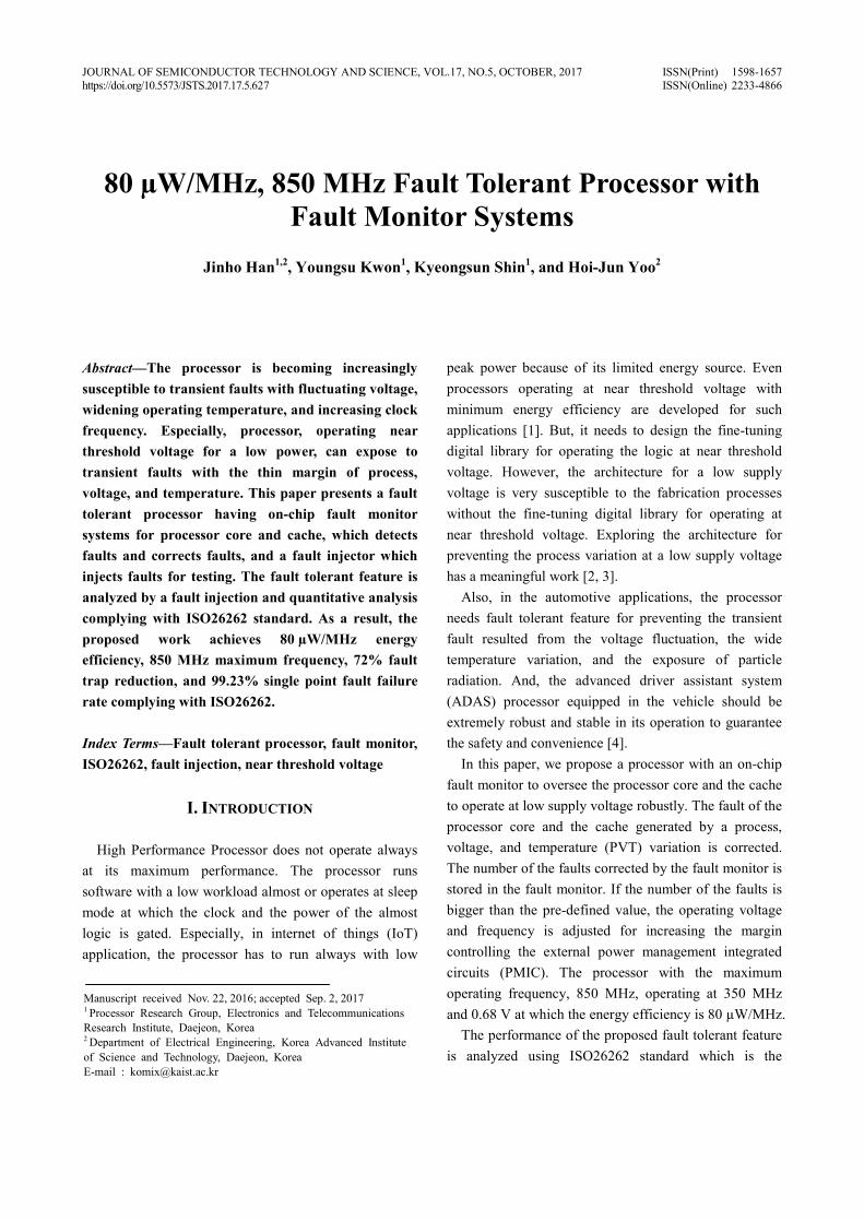
Fig. 1 illustrates the proposed processor architecture without a fault tolerant feature. The processor architecture, named ALDEBARAN targets 850 MHz operating frequency at 65 nm technology node and 2-issue superscalar architecture getting sufficient performance for processing ADAS algorithm. The memory access time is reduced with the 32KB Instruction and data cache of which 99% hit rate is accomplished, and memory management unit (MMU) with a table look-aside buffer (TLB) which stores 8 instruction and data entry, is for supporting the virtual addressing. And, for that the critical path is below 1.2 ns, the processor has 13 pipeline stages. In fetch scheduler
(FS), the instruction is fetched more than two instructions, so in two execution units, two instructions ca run simultaneously.
The stall by a control instruction is prevented by adopting branch target buffer (BTB) and branch prediction (BP). BP is using the GSHARE method with branch history registers. And, BTB with 256-entry is addressing with a program counter (PC). And, there is the calculation logic using register and offset in BP stage for reducing the time processing the decision. FS requests eight instructions at the maximum from the instruction cache. These instructions are saved in the instruction queue (IQ). The integer execution unit has tow. So, In SB (Score Board), the dependency for two instructions is checked. If the dependency doesn’t exist, two instructions are issued into two integer execution units, named integer unit 0 (IU0) and integer unit 1 (IU1). So, the average instructions per clock (IPC) is accomplished 1.3.
With on-chip debugger, the software development environment (SDE) is developed using Eclipse platform. And, firmware level software can be developed with µlib and Linux is ported with the kernel version 3.0. Because the compiler is developed based on the GNU compiler, the gnu tools are supported at ALDEBARAN.
Because the energy efficiency has 80 µW/MHz per core, the processor was included to develop SoC for black box, robot, IoT, and power-metering. In this paper,
Fig. 1. the base processor architecture without a fault tolerant feature having VA(Virtual Addressing), BTB(Branch Target Buffer), BP(Branch Prediction), FS(Fetch Scheduler), IQ(Instruction Queue), D0U(Decoding unit 0 of the Upside), D1U(Decoding unit 1 of the Upside), D0D(Decoding unit 0 of the Downside), D1D(Decoding unit 0 of the Downside), S(Scheduler), SB(Score Board), EQ(Execution), EP(Execution Prolog), IU0(Integer Unit0), IU2, FPU(Floating Point Unit), LS(Load/Store), RF(Register File), TLB(Table Look-aside Buffer), iCache(instruction Cache), and dCache(data Cache).
JOURNAL OF SEMICONDUCTOR TECHNOLOGY AND SCIENCE, VOL.17, NO.5, OCTOBER, 2017 629
the fault tolerant feature is added to apply with the automotive application.
III. FAULT TOLERANT FEATURE
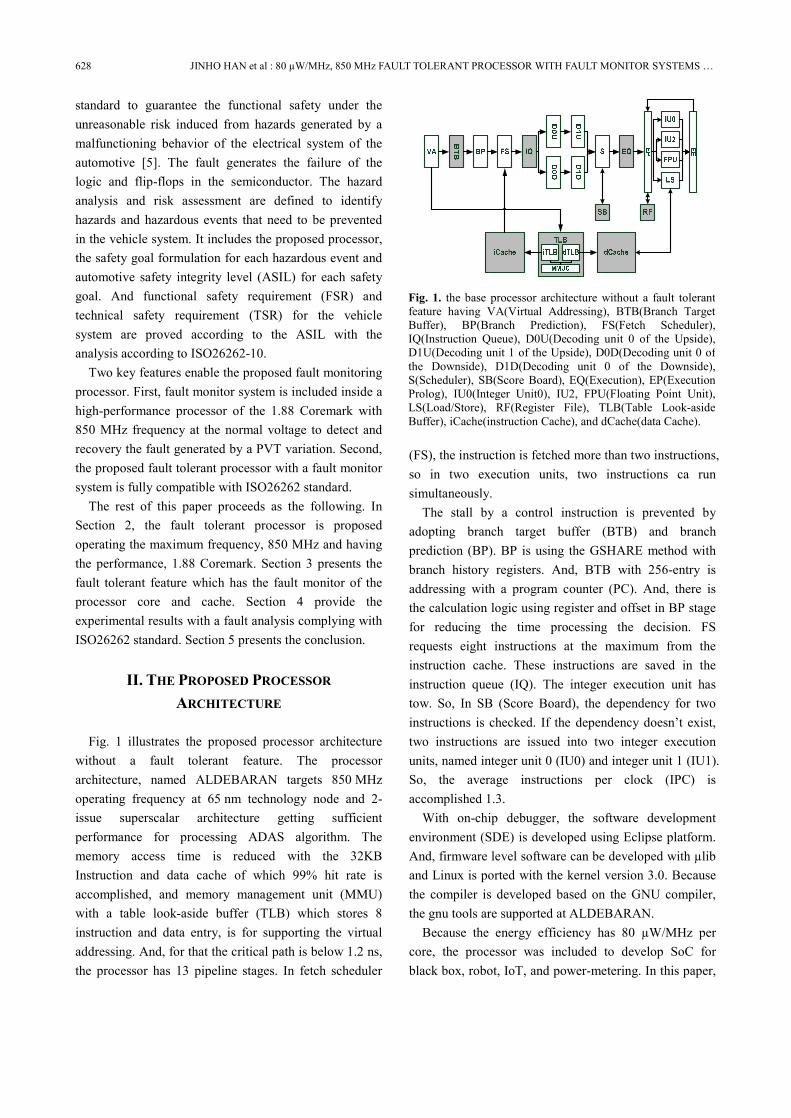
The fault tolerant feature of the processor is composed of the fault monitor of the processor core and the cache, the external fault monitor with fault counter, and failure recovery as illustrated in Fig. 2. Each fault monitors of the processor core and the cache collect the fault information in the processor core and the cache. The fault monitor system including 4 fault monitors doesn’t operate with the separated low voltage. It operates at the core voltage and the frequency of the clock which is low sufficiently not to generate the fault. External fault monitor collects the output of fault monitors in the processor core and the cache which includes the fault type and the fault region. And, the fault type is composed
of the silent fault and severe fault, the fault region is composed of the modules with the fault in the processor core and cache. The silent fault is defined the fault which is generated but corrected by the fault monitor in the processor core and cache or does not induce malfunctions of the processor core and cache.
The severe fault is defined the fault which is generated, but is not corrected by the fault monitor in the processor core and cache or induces malfunctions of the processor core and cache.
Each fault is counted using the internal counter in the external fault manager and the fault prediction is sent to the failure recovery to control the margin when the value of the counts is bigger than the threshold value which can be programmed by the software considering the characteristics of the System Environment, and the severe fault which is not corrected in the fault monitor, is sent to the failure recovery to recover the processor. The failure recovery prevents the failure of the processor by controlling the external PMIC, Phase Locked Loop (PLL), using the fault prediction of the external fault monitor and recovers the processor by resetting the processor with a fault.
Fault injection system including one fault injection controller and three fault injectors injects faults in processor core and caches for a fault injection analysis. Each fault injector is controlled by fault injection controller, which has the joint test action group (JTAG) interface, and on-chip debugger software. We send the fault injection information using on-chip debugger with information of frequency, interval, and target module and inject faults immediately using terminal of on-chip debugger.
We introduce each fault tolerant feature of the processor core and the cache in the following sub chapter.
1. Processor Core
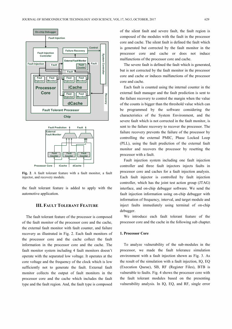
To analyze vulnerability of the sub-modules in the
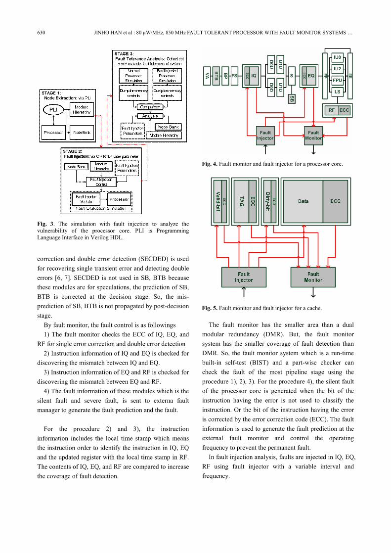
processor, we made the fault tolerance simulation environment with a fault injection shown as Fig. 3. As the result of the simulation with a fault injection, IQ, EQ (Execution Queue), SB, RF (Register Files), BTB is vulnerable to faults. Fig. 4 shows the processor core with the fault tolerant modules based on the presenting vulnerability analysis. In IQ, EQ, and RF, single error
External Fault Monitor
Fault Counter
Fault Counter
Fault Counter
Processor Core iCache dCache
Fault Prediction Fault
Chip
Fault Tolerant Processor
Processor Core
iCache
Faut Monitor
Faut Injector
Faut Monitor
dCache
Fault Injection Controller
Failure Recovery
External Fault Monitor
Faut Monitor
Faut Injector
Faut Injector
On-chip Debugger
Fault Counter
System
Controller
Recovery
Control
Fault Injection
Fault Injection FaultFault
Fault
Fig. 2. A fault tolerant feature with a fault monitor, a fault injector, and recovery module.
630 JINHO HAN et al : 80 µW/MHz, 850 MHz FAULT TOLERANT PROCESSOR WITH FAULT MONITOR SYSTEMS …
correction and double error detection (SECDED) is used for recovering single transient error and detecting double errors [6, 7]. SECDED is not used in SB, BTB because these modules are for speculations, the prediction of SB, BTB is corrected at the decision stage. So, the mis-prediction of SB, BTB is not propagated by post-decision stage.
By fault monitor, the fault control is as followings 1) The fault monitor checks the ECC of IQ, EQ, and
RF for single error correction and double error detection 2) Instruction information of IQ and EQ is checked for
discovering the mismatch between IQ and EQ. 3) Instruction information of EQ and RF is checked for
discovering the mismatch between EQ and RF. 4) The fault information of these modules which is the
silent fault and severe fault, is sent to externa fault manager to generate the fault prediction and the fault.
For the procedure 2) and 3), the instruction
information includes the local time stamp which means the instruction order to identify the instruction in IQ, EQ and the updated register with the local time stamp in RF. The contents of IQ, EQ, and RF are compared to increase the coverage of fault detection.
The fault monitor has the smaller area than a dual modular redundancy (DMR). But, the fault monitor system has the smaller coverage of fault detection than DMR. So, the fault monitor system which is a run-time built-in self-test (BIST) and a part-wise checker can check the fault of the most pipeline stage using the procedure 1), 2), 3). For the procedure 4), the silent fault of the processor core is generated when the bit of the instruction having the error is not used to classify the instruction. Or the bit of the instruction having the error is corrected by the error correction code (ECC). The fault information is used to generate the fault prediction at the external fault monitor and control the operating frequency to prevent the permanent fault.
In fault injection analysis, faults are injected in IQ, EQ, RF using fault injector with a variable interval and frequency.
Fig. 4. Fault monitor and fault injector for a processor core.
Fig. 5. Fault monitor and fault injector for a cache.
Fig. 3. The simulation with fault injection to analyze the vulnerability of the processor core. PLI is Programming Language Interface in Verilog HDL.
JOURNAL OF SEMICONDUCTOR TECHNOLOGY AND SCIENCE, VOL.17, NO.5, OCTOBER, 2017 631
2. Cache A fault tolerant cache system is composed of three
architectures. The fault tolerant cache system is composed of 1) the error correction code of the memory and 2) the fault manager, and 3) the fault injector as Fig. 5.
The memory in the cache are tag memory which saves the tag, which is the most significant bit of an address, data memory which saves 8-word’s data addressing by the least significant bit of an address, dirty-bit memory which informs being written by the processor, valid-bit memory which is whether data memory includes the 8-word’s data.
All the caches for supporting the fault tolerant functions have the ECC. We used SECDED. We have to use the 8-bit data chunk for a low latency access by a byte. In case of SECDED, the redundant bit is 5-bits. We added the error correction function using the characteristics of the cache by the fault manager.
First, the valid-bit’s error is checked. If there are errors in the valid-bits, the dirty-bit’s value is checked. If dirty-bits in all ways are 0, the lines will be invalid and the requested data is recovered by reading the data from SDRAM. But, if dirty-bits aren’t 0 in any ways, the data written by the processor can’t recover by an error, the fault trap is generated.
Second, if there are no error in the valid-bits, the tag’s error is checked. When there is a hit way, the dirty-bit of a hit way is checked if there is the tag’s error. If dirty-bit of a hit way is 0, the lines will be invalid and the requested data is recovered by reading it from SDRAM. If dirty-bit is 1, the fault trap is generated. When there is a miss, the data is recovered by invalidating the line of
all ways if the dirty-bits of all way is 0 although tag of any way has an error. But, if dirty-bit is 1, the fault trap is generated.
Third, when tag has no error and there is a hit way, the data is recovered by the invalidation and reading SDRAM if the dirty-bit is 0 although there is an error in the line of the hit way. And, although tag has no error and there is no hit way, the fault trap can be generated if the LRU way has an error. But, if the dirty-bit is 0 for the LRU way, the data is recovered by invalidating the LRU way.
IV. IMPLEMENTATION RESULTS
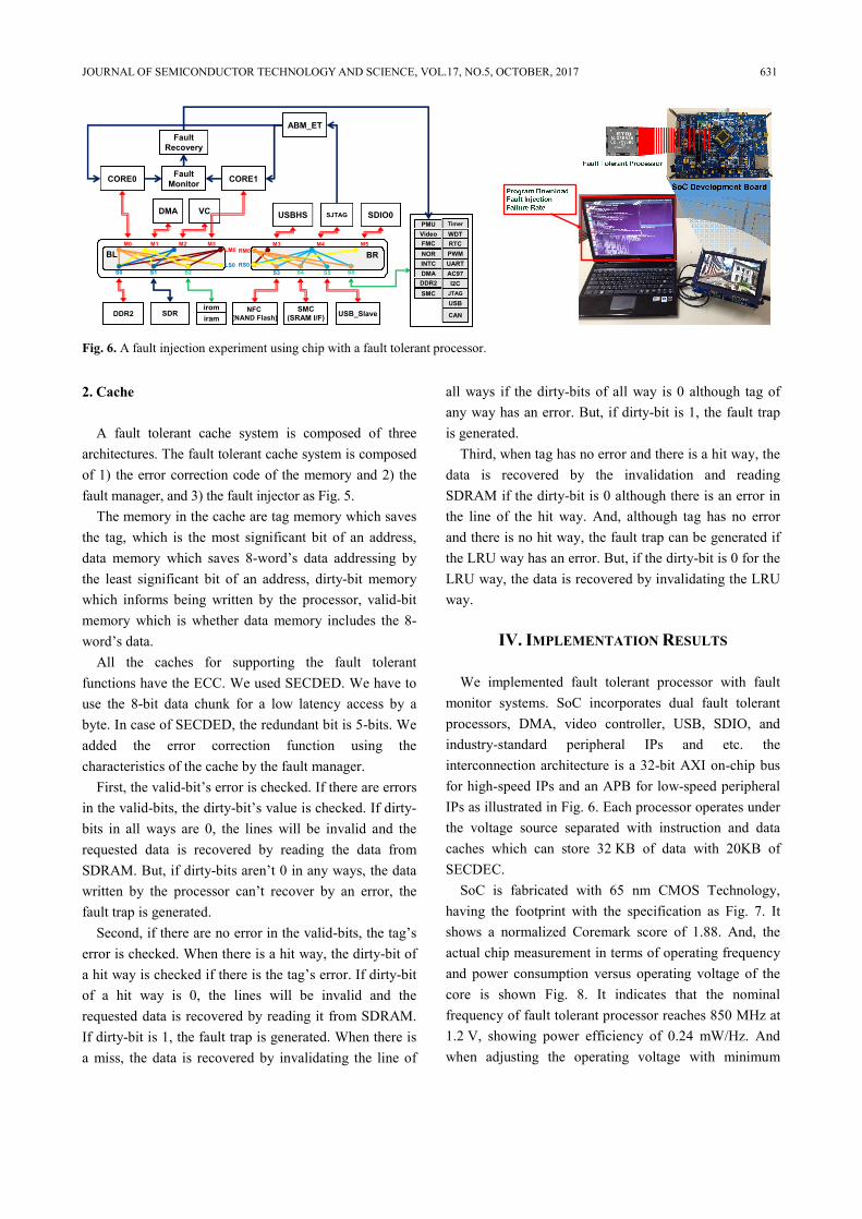
We implemented fault tolerant processor with fault monitor systems. SoC incorporates dual fault tolerant processors, DMA, video controller, USB, SDIO, and industry-standard peripheral IPs and etc. the interconnection architecture is a 32-bit AXI on-chip bus for high-speed IPs and an APB for low-speed peripheral IPs as illustrated in Fig. 6. Each processor operates under the voltage source separated with instruction and data caches which can store 32 KB of data with 20KB of SECDEC.
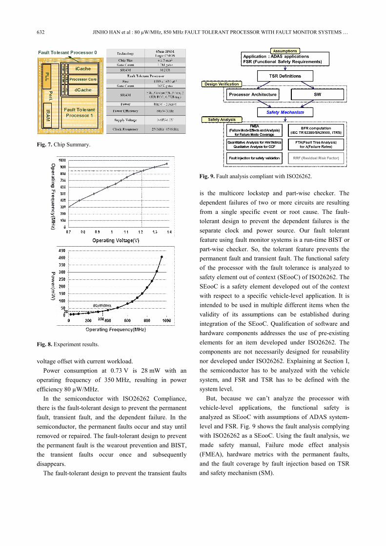
SoC is fabricated with 65 nm CMOS Technology, having the footprint with the specification as Fig. 7. It shows a normalized Coremark score of 1.88. And, the actual chip measurement in terms of operating frequency and power consumption versus operating voltage of the core is shown Fig. 8. It indicates that the nominal frequency of fault tolerant processor reaches 850 MHz at 1.2 V, showing power efficiency of 0.24 mW/Hz. And when adjusting the operating voltage with minimum
M0 M2
S0 S1 S2
M4
VC SJTAG
DDR2 SDR
CORE0
PMU Timer
S6
M1
DMA
S4
SMC(SRAM I/F)
INTC
M3
USBHS
iromiram
S3
NFC(NAND Flash)
S5
USB_Slave
DMADDR2
LS0
LM0
RS0
RM0BL BR
SMC
VideoM5
SDIO0
FMCWDT
NORM3
CORE1
RTC
UARTAC97I2C
JTAG
PWM
USB
CAN
Fault Monitor
Fault Recovery
ABM_ET
Fig. 6. A fault injection experiment using chip with a fault tolerant processor.
632 JINHO HAN et al : 80 µW/MHz, 850 MHz FAULT TOLERANT PROCESSOR WITH FAULT MONITOR SYSTEMS …
voltage offset with current workload. Power consumption at 0.73 V is 28 mW with an
operating frequency of 350 MHz, resulting in power efficiency 80 µW/MHz.
In the semiconductor with ISO26262 Compliance, there is the fault-tolerant design to prevent the permanent fault, transient fault, and the dependent failure. In the semiconductor, the permanent faults occur and stay until removed or repaired. The fault-tolerant design to prevent the permanent fault is the wearout prevention and BIST, the transient faults occur once and subsequently disappears.
The fault-tolerant design to prevent the transient faults
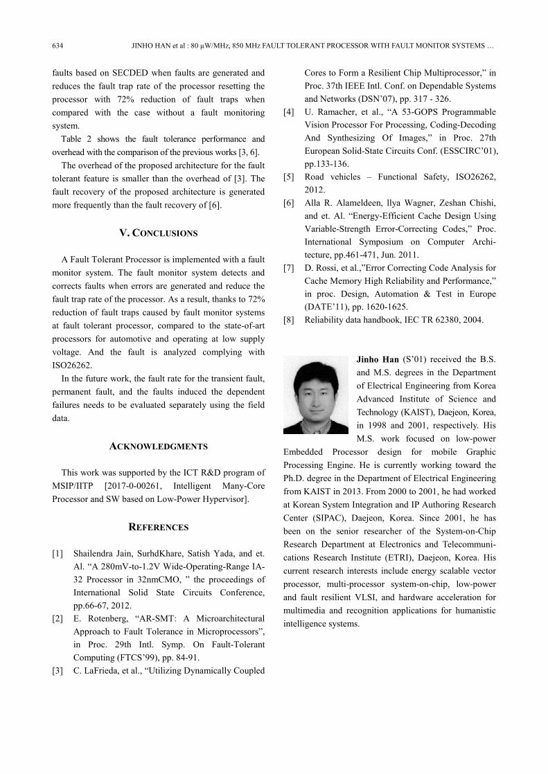
is the multicore lockstep and part-wise checker. The dependent failures of two or more circuits are resulting from a single specific event or root cause. The fault-tolerant design to prevent the dependent failures is the separate clock and power source. Our fault tolerant feature using fault monitor systems is a run-time BIST or part-wise checker. So, the tolerant feature prevents the permanent fault and transient fault. The functional safety of the processor with the fault tolerance is analyzed to safety element out of context (SEooC) of ISO26262. The SEooC is a safety element developed out of the context with respect to a specific vehicle-level application. It is intended to be used in multiple different items when the validity of its assumptions can be established during integration of the SEooC. Qualification of software and hardware components addresses the use of pre-existing elements for an item developed under ISO26262. The components are not necessarily designed for reusability nor developed under ISO26262. Explaining at Section I, the semiconductor has to be analyzed with the vehicle system, and FSR and TSR has to be defined with the system level.
But, because we can’t analyze the processor with vehicle-level applications, the functional safety is analyzed as SEooC with assumptions of ADAS system-level and FSR. Fig. 9 shows the fault analysis complying with ISO26262 as a SEooC. Using the fault analysis, we made safety manual, Failure mode effect analysis (FMEA), hardware metrics with the permanent faults, and the fault coverage by fault injection based on TSR and safety mechanism (SM).
Fig. 7. Chip Summary.
Fig. 8. Experiment results.
Fig. 9. Fault analysis compliant with ISO26262.

JOURNAL OF SEMICONDUCTOR TECHNOLOGY AND SCIENCE, VOL.17, NO.5, OCTOBER, 2017 633
In FMEA, failure mode and the effect of the failure mode are found. The failure mode is a manner in which an element or an item fails. Finding the failure mode by a sub-module and the effect is found by the fault ratio with the area. So, the bigger is the product of single point fault ratio and area, the more often is the fails generated. We can reduce the effect of the failure modes in the processor for the SM using fault monitor systems being analyzed with FMEA.
Hardware metric as single point fault metric (SPFM) is calculated using a base fault rate (BFM) calculated by using IEC62380 standards [8], the fraction of the safe fault, the diagnostic coverage which is proportion of the hardware element failure rate that is detected or controlled by the implemented safety mechanisms. We assume there is not the safe fault at all the sub module. SPFM is low by this assumption. The diagnostic coverage is solved by the fault injection experiment
shown as Fig. 6. Our safety mechanism(SM) is the fault monitor system.
We can find the fault rate by using the fault injector when the SM is applied. As shown at Table 1 and Fig. 10, the single point faults metric about the permanent faults is 99.23%, and the latent faults metric about the permanent faults is 93.64% with our safety mechanism including the fault monitor systems. For ASIL D of ISO26262, SPFM is achieved more than 90%. So, our design can have SPFM about the permanent faults for ASIL D.
Using the fault injection experiment, the fault rate is measured at the Table 1. The fault represented the transient fault, the permanent fault, and faults which induced dependent failures. The hit rate of the proposed architecture is not changed but, I think the recovery case in the cache is increased by the fault monitor and the recovery case by the safe faults is showed the miss case because of reading the data from SDRAM. If the cache access case is classified to the cache hit, the cache miss with the safe fault, the access with the severe fault. This cache miss with the safe fault is increased and the hit rate is reduced but, the severe fault is reduced with the factor 72% by changed the severe fault to the safe fault by increasing the recovery cases using the fault monitor. So, I think the hit rate will be reduced and the access time be increased. But, the hit rate is not changed at the simulation and experiment with the fault injection because the access case with the fault is very small when compared to the overall access case.
Also, the fault monitoring system detects and corrects
Fig. 10. fault tolerant performance vs. 100 fault injections.
Table 1. fault tolerant performance and cache performance
Performance Parameter No FTF The proposed Fault Traps 84 30
Sieve Hit Ratio 99.3 99.3
Fault Traps 83 29 Bubble
Hit Ratio 99.3 99.4 Fault Traps 83 28
Mp3 Hit Ratio 99.3 99.2
Fault Traps 70 25 Mpeg2
Hit Ratio 98.5 98.4 Fault Traps 90 30
Coremark Hit Ratio 98.4 98.4
Fault Traps 92 30 FPmark
Hit Ratio 98.1 98.1 Coremark 1.88 Coremark/MHz
SPFM 99.23
Table 2. Fault Tolerance Performance Comparison
No FTF FT Cache [6] DCC [3] The proposed Fault Detection
Coverage N/A Medium High Medium ~ High
ECC X SECDED N/A SECDED
Fault Detection X ECC DMR Fault Monitor System
Area Overhead X > 1.6 x Cache 2 x Cores 1.6 x Cache Fault Detection
Time X 1 cycle 137 cycles 1 cycle
Fault Prediction X X Thread Control
Error Predictor Clock/
Voltage Control Fault Injection X X X O
Fault Traps 100% 83% N/A 28% Single Point
Fault X N/A N/A 99.23%
634 JINHO HAN et al : 80 µW/MHz, 850 MHz FAULT TOLERANT PROCESSOR WITH FAULT MONITOR SYSTEMS …
faults based on SECDED when faults are generated and reduces the fault trap rate of the processor resetting the processor with 72% reduction of fault traps when compared with the case without a fault monitoring system.
Table 2 shows the fault tolerance performance and overhead with the comparison of the previous works [3, 6].
The overhead of the proposed architecture for the fault tolerant feature is smaller than the overhead of [3]. The fault recovery of the proposed architecture is generated more frequently than the fault recovery of [6].
V. CONCLUSIONS
A Fault Tolerant Processor is implemented with a fault monitor system. The fault monitor system detects and corrects faults when errors are generated and reduce the fault trap rate of the processor. As a result, thanks to 72% reduction of fault traps caused by fault monitor systems at fault tolerant processor, compared to the state-of-art processors for automotive and operating at low supply voltage. And the fault is analyzed complying with ISO26262.
In the future work, the fault rate for the transient fault, permanent fault, and the faults induced the dependent failures needs to be evaluated separately using the field data.
ACKNOWLEDGMENTS
This work was supported by the ICT R&D program of MSIP/IITP [2017-0-00261, Intelligent Many-Core Processor and SW based on Low-Power Hypervisor].
REFERENCES
[1] Shailendra Jain, SurhdKhare, Satish Yada, and et. Al. “A 280mV-to-1.2V Wide-Operating-Range IA-32 Processor in 32nmCMO, ” the proceedings of International Solid State Circuits Conference, pp.66-67, 2012.
[2] E. Rotenberg, “AR-SMT: A Microarchitectural Approach to Fault Tolerance in Microprocessors”, in Proc. 29th Intl. Symp. On Fault-Tolerant Computing (FTCS’99), pp. 84-91.
[3] C. LaFrieda, et al., “Utilizing Dynamically Coupled
Cores to Form a Resilient Chip Multiprocessor,” in Proc. 37th IEEE Intl. Conf. on Dependable Systems and Networks (DSN’07), pp. 317 - 326.
[4] U. Ramacher, et al., “A 53-GOPS Programmable Vision Processor For Processing, Coding-Decoding And Synthesizing Of Images,” in Proc. 27th European Solid-State Circuits Conf. (ESSCIRC’01), pp.133-136.
[5] Road vehicles – Functional Safety, ISO26262, 2012.
[6] Alla R. Alameldeen, llya Wagner, Zeshan Chishi, and et. Al. “Energy-Efficient Cache Design Using Variable-Strength Error-Correcting Codes,” Proc. International Symposium on Computer Archi- tecture, pp.461-471, Jun. 2011.
[7] D. Rossi, et al.,”Error Correcting Code Analysis for Cache Memory High Reliability and Performance,” in proc. Design, Automation & Test in Europe (DATE’11), pp. 1620-1625.
[8] Reliability data handbook, IEC TR 62380, 2004.
Jinho Han (S’01) received the B.S. and M.S. degrees in the Department of Electrical Engineering from Korea Advanced Institute of Science and Technology (KAIST), Daejeon, Korea, in 1998 and 2001, respectively. His M.S. work focused on low-power
Embedded Processor design for mobile Graphic Processing Engine. He is currently working toward the Ph.D. degree in the Department of Electrical Engineering from KAIST in 2013. From 2000 to 2001, he had worked at Korean System Integration and IP Authoring Research Center (SIPAC), Daejeon, Korea. Since 2001, he has been on the senior researcher of the System-on-Chip Research Department at Electronics and Telecommuni- cations Research Institute (ETRI), Daejeon, Korea. His current research interests include energy scalable vector processor, multi-processor system-on-chip, low-power and fault resilient VLSI, and hardware acceleration for multimedia and recognition applications for humanistic intelligence systems.
JOURNAL OF SEMICONDUCTOR TECHNOLOGY AND SCIENCE, VOL.17, NO.5, OCTOBER, 2017 635
Youngsu Kwon (M’02) was received B.S., M.S., and Ph.D. degrees from Korea Advanced Institute of Science and Technology (KAIST), Republic of Korea in 1997, 1999, and 2004, respectively. He had been with Microsystems Technology
Laboratory (MTL), Massachusetts Institute of Technology as a Postdoctoral Associate from 2004 to 2005 for designing 3-Dimensional FPGA. He is now with Intelligent SoC Research Department, Electronics and Telecommunications Research Institute (ETRI), Republic of Korea, since 2005. In ETRI, he is a Group Manager, Principal Research Staff of the Processor Research Group devoted to the design of processor, AB. He has special interests in many-core architecture, low-power processor design, computer-aided design, and algorithmic optimizations of circuits and systems. He received Presidential Prize from Korean Government in 2016, Official Commendations from the Ministry of Science and ICT as well as Ministry of Industry in 2016, the Excellent Researcher Award from Korea Research Council in 2013, Industrial Contributor Award from Korean Federation of SMEs in 2013, and medals from Samsung’s Thesis Prizes in 1997 and 1999.
Kyoungseon Shin received the B.S. and M.S. degrees in the Department of Electrical Engineering from Chonbuk National University, Jeonju, Korea in 1989 and 1991, respectively. His M.S work focused on BIST (Built-in Self Test) circuit design for
fast testing of Mega-bit DRAM. From 1991 to 1999, he had worked at LG semiconductor Co.,Ltd, Korea. While working for LG Semiconductor, he was involved in designing MCU(Micro Controller Unit) and MDS (Micom Development System). Since 1999, He has been with System-on-Chip Research Department, Electronics and Telecommunications Research Institute (ETRI), Daejeon, Korea.His current research interests include the development of multimedia processor, multi-cores, low-power embedded processor, autonomouse driving processor.
Hoi-Jun Yoo (M’95–SM’04–F’08) graduated from Electronic Depart- ment of Seoul National University, Korea, and received M.S. and Ph.D. degrees from Electrical Engineering, Korea Advanced Institute of Science and Technology (KAIST), Daejeon.
He was the VCSEL pioneer in Bell Communications Research at Red Bank, NJ. USA and Manager of DRAM design group at Hyundai Electronics designing from 1M DRAM to 256M SDRAM. Currently, he is a full professor of Department of Electrical Engineering at KAIST and the director of the System Design Innovation and Application Research Center (SDIA). From 2003 to 2005, he served as the full time Advisor to the Minister of Korean Ministry of Information and Communication for SoC and Next Generation Computing. His current research interests are bio inspired IC design, network on a chip, multimedia SoC design, wearable healthcare systems, and high speed and low power memory. He has published more than 250 papers, and wrote or edited 5 books, DRAM Design (1997, Hongneung), High Performance DRAM (1999 Hongneung), Low Power NoC for High Performance SoC Design (2008, CRC), Mobile 3D Graphics SoC (2010, Wiley), and BioMedical CMOS ICs (coedited with Chris Van Hoof, 2010, Springer), and many chapters of books. Dr. Yoo received the Korean National Medal for his contribution to Korean DRAM Industry in 2011, the Electronic Industrial Association of Korea Award for his contribution to DRAM technology the 1994, Hynix Development Award in 1995, the Korea Semiconductor Industry Association Award in 2002, Best Research of KAIST Award in 2007, Design Award of 2001 ASP-DAC, Outstanding Design Awards of 2005, 2006, 2007, 2010, 2011 A-SSCC, and Korean Scientist of the Month Award (Dec. 2010). He is a member of the executive committee of Symposium on VLSI, and A-SSCC. He was the TPC chair of the A-SSCC 2008, a guest editor of IEEE JSSC and IEEE T-BioCAS. He was the TPC Chair of ISWC (International Symposium on Wearable Computer) 2010, IEEE Fellow, IEEE Distinguished Lecturer (’10–’11), Far East Chair of ISSCC (’11–’12 Technology Direction Sub-Committee Chair of ISSCC (’13), TPC Vice Chair of ISSCC (’14), and TPC Chair of ISSCC (’15).