8 digifl'.11 cth:uits and devices - department of...
TRANSCRIPT

8 Digifl'.11 Cth:uits and devices
8.1 Introduction
In analog electronics, voltage is a continuous variable. This is useful because
most physical quantities we encounter are continuous: sound levels, light intensity,
temperature, pressure, etc.1 Digital electronics, in contrast, is characterized by only
two distinguishable voltages. These two states are called by various names: on/off,
true/false, high/low, and 1/0. In practice, these two states are defined by the circuit
voltage being above or below a certain value. Fbr example, in TTL logic circuits,
a high state corresponds to a voltage above 2.0 V, while a low state is defined as a
voltage below 0.8 V.2
The virtue of this system is illustrated in Fig. 8.1. We plot the voltage level
·versus time for some electronic signal. If this was part of an analog circuit, we
would say that the voltage was averaging about 3 V, but that it had, roughly, a 20%
noise level, rather large for most applications and thus unacceptable . For a TTL
digital circuit, however, this signal is always above 2.0 V and is thus always in
the high state. There is no uncertainty about the digital state of this voltage, SC' the
digital sig'llal has zero noise. This is the primary advantage of digital electronic8: it
is relatively immune to the noise that is ubiquitous in elech·onic circuits. Of comse,
if the fluctuations in Fig. 8.1 became so large that the voltage dipped below 2.0 V,
then even a digital circuit would have problems.
8.2 Binary numbers
Although digital circuits have excellent noise immunity, they also are limited to
producing only two levels. This does not appear to be very helpful in representing
the continuous signals we so frequently encounter. The solution starts with the
1 This holds for most macroscopic quantities. On the atomic level, many physical quantities are quantized. 2 If the voltage is between these thresholds, we say the state is undetermined, which means the circuit
behavior cannot be insured.

;eful because
ight intensity,
:rized by only
ames: on/off,
by the circuit
logic circuits,
s defined as a
voltage level
,g circuit, we
ughly, a20%
e. For a TTL
ms always in
oltage, so the
~lectronics : it
ts . Of course,
below 2.0 V,
tre limited to
representing
arts with the
es are quantized. ns the circuit
·'
8.2 Binary numbers
Table 8.1 The first twelve counting numbers in binary
Base 10 Base 2
0 0
1
2 10
3 11
4 100
5 101
Base 10
6 7 8
9 10
11
Base 2
110
111
1000
1001
1010
1011
) t Figure 8.1 A noisy analog signal is noise-free in digital.
realization that we can represent a signal level by a number that only uses two
digits . For these binary numbers, the two digits used are 0 and L Binary numbers
are also call, bas~ 2 numbers, and can be understood by abstractin~ the rules we
all know for the numbers we cominonly use (base 10 numbers): Wl\e'n we write
down a base 10 number, each digit can have 10 possible values, 0 to 9, and each
digit corresponds to 10 raised to a power. For example, when I write 10241 o, this
is equal to
.. 102410 = 1 x 10³ + 0 x 102 + 2 x 101 +4 x 10° (8.1)
where we use the subscript 10 on 1024 to make explicit the base of the number.
Analogously, for binary numbers, each digit can have only 2 possible values, 0
or 1, and each digit of the number corresponds to 2 raised to a power. Thus
101102 = 1x24 +0 x 23 + 1 x 22 + 1 x 21 + 0 x 2° = 2210 . (8.2)
The first twelve base 10 numbers and their binary equivalents are given in
Table 8.1.
In a similar manner, the rules for base 10 addition and subtraction can be mapped
over to binary arithmetic. Some examples are shown in Table 8.2. In base 10, when
we add the rightmost column, 9 plus 5 equals 14. Since this result cannot be
expressed in a single digit with the ten available digits (0 to 9), we write down the
4 and carry the 1 to the next column. Similarly, when we add the 1 and 1 of the
rightmost column of the binary number, we get 102. Since this cannot be expressed
Digital circuits and devices
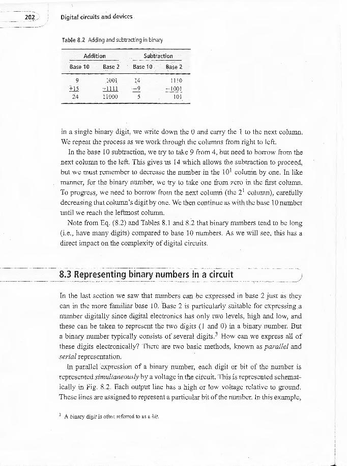
Table 8.2 Adding and subtracting in binary
Addition Subtraction
Base 10 Base 2 Base 10 Base 2
9 1001 14 1110 +15 + 1111 -9 -1001
24 11000 5 101
in a single binary digit, we write down the 0 and carry the 1 to the next column.
We repeat the process as we work through the columns from right to left.
In the base 10 subtraction, we try to take 9 from 4, but need to borrow from the
next column to the left. This gives us 14 which allows the subtraction to proceed,
but we must remember to decrease the number in the 101 column by one. In like
manner, for the binary number, we try to take one from zero in the first column.
To progress, we need to borrow from the next column (the 21 column), carefully
decreasing that column's digit by one. We then continue as with the base 10 number
until we reach the leftmost column.
Note from Eq. (8 .2) and Tables 8.1 and 8.2 that binary numbers tend to be long
(i.e., have many digits) compared to base 10 numbers. As we will see, this has a
direct impact on the complexity of digital circuits.
8.3 Representing binary numbers in a circuit
In the last section we saw that numbers can be expressed in base 2 just as they
can in the more familiar base 10. Base 2 is particularly suitable for expressing a
number digitally since digital electronics has only two levels, high and low, and
these can be taken to represent the two digits (1 and 0) in a binary number. But
a binary number typically consists of several digits. 3 How can we express all of
these digits electronically? There are two basic methods, known as parallel and
serial representation.
In parallel expression of a binary number, each digit or bit of the number is
represented simultaneously by a voltage in the circuit. This is represented schemat
ically in Fig. 8.2 . Each output line has a high or low voltage relative to ground.
These lines are assigned to represent a particular bit of the number. In this example,
3 A binary digit is often referred to as a bit.

: column.
from the
proceed,
e. In like
column.
carefully
)number
) be long
his has a
: as they
·essing a
low, and
ber. But
ss all of
zllel and
tmber is
chemat
ground.
xample,
t
I
l I l l l
v
Digital
Circuit
8.3 Representing binary numbers in a circuit ( 703
23
22
21
20
Outputs:
~
~
-- 0
-Figure 8.2 Parallel representation of a four-bit number 1101 .
bit:
]~~~D-·t Figure 8.3 Serial representation of a four-bit number 1011 .
the bottom line represents the 2° bit, the next line up represents the 21 bit, and
so on. Because we have four independent lines, the entire four-bit number can be
expressed at a point in time, so parallel communication of information is very fast.
The price we pay for this speed is the increased number of lines in our circuit. The
more precision we want in our number, the more significant figures we need, and
the more lines are required.
An alternative way of expressing a binary number is by a serial representation.
In this method, the various bits are communicated by sending a time sequence of
high/low voltage levels on a single line. An example of this is shown in Fig. 8.3 .
The plot shows the voltage level on a serial line. The voltage switches between
high and low levels, with each level lasting for a certain time interval. The first
interval corresponds to the 2° bit of our number, the next interval represents the
21 bit, and so on. We are thus able to communicate the binary number on a single
line, rather than the multiple lines required for parallel communications, but the
communication is no longer instantaneous; we must wait for several intervals
before we receive all the bits of our transmitted number.
In order for serial transmission of information to work, both the sender and
receiver need to agree about several things . Some of these are: (1) how many bits
of data are going to be sent, (2) what digital level (high or low) corresponds to
the 1 bit, (3) what is the time interval between bits, and ( 4) how will the start of a
number be recognized?
Digital circuits and devices
8.4 logic gates
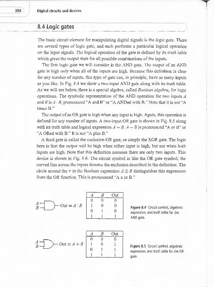
The basic circuit element for manipulating digital signals is the logic gate. There are several types of logic gate, and each performs a particular logical operation
on the input signals. The logical operation of the gate is defined by its truth table
which gives the output state for all possible combinations of the inputs. The first logic gate we will consider is the AND gate. The output of an AND
gate is high only when all of the inputs are high. Because this definition is clear for any number of inputs, this type of gate can, in principle, have as many inputs as you like. In Fig. 8.4 we show a two-input AND gate along with its truth table. As we will see below, there is a special algebra, called Boolean algebra, for logic
operations. The symbolic representation of the AND operation for two inputs A
and Bis A · B, pronounced "A and B" or "A ANDed with B." Note that it is not "A times B."
The output of an OR gate is high when any input is high. Again, this operation is defined for any number of inputs. A two-input OR gate is shown in Fig. 8.5 along
with its truth table and logical expression A + B. A +Bis pronounced "A or B" or "A ORed with B." It is not "A plus B."
A third gate is called the exclusive-OR gate, or simply the XOR gate. The logic
here is that the output will be high when either input is high, but not when both inputs are high. Note that this definition assumes there are only two inputs . This device is shown in Fig. 8.6. The circuit symbol is like the OR gate symbol; the
curved line across the inputs denotes the exclusion described in the definition. The
circle around the + in the Boolean expression A EB B distinguishes this expression from the OR function. This is pronounced "Ax or B."
A
~=[)-out=A·B 0 1 0 1
A
~=[)-out=A+B 0 1 0 1
B 0 0 1 1
B 0 0 1 1
Out 0 0 0 1
Out 0 1 1 1
Figure 8.4 Circuit symbol, algebraic expression, and truth table for the AND gate.
Figure 8.5 Circuit symbol, algebraic expression, and truth table for the OR gate.

~ate. There I operation truth table
)fan AND
[on is clear
tany inputs truth table.
a, for logic
'O inputs A
it is not "A
Jperation is
~· 8.5 along 'A or B" or
:. The logic
when both
nputs. This ymbol; the
nition. The
expression
10/, algebraic J/e for the
10/, algebraic lie for the OR
T l l i
I l j
! I I I l l
1 j l
I l 4
i
I j
i l l
I l
~~D-Out=AEBB
A-t>--Out =A
A~ -B ----L___/' Out = A · B
A~ -B~Out=A+B
A 0 1 0 1
A 0 1 0 1
A 0 1 0 1
B 0 0 1 1
B 0 0 1 1
B 0 0 1 1
Out 0 1 1 0
Out 1 1 1 0
Out 1 0 0 0
8.4 Logic gates
Figure 8.6 Circuit symbol, algebraic expression, and truth table for the XOR gate.
Figure 8.7 Circuit symbol, algebraic expression, and truth table for the buffer gate.
Figure 8.8 Circuit symbol, algebraic expression, and truth table for the NANO gate.
Figure 8.9 Circuit symbol, algebraic expression, and truth table for the NOR gate.
The buffer gate, shown in Fig. 8.7, seems to be superfluous. It has only one
input, and the output is the same as the input. What good is this? This gate is
used to regenerate logic signals. A logical high signal may start out at 5 V, say, but after being transmitted on conductors with non-zero resistance or after driving several other logic gates, the voltage level may fall and become perilously close
to the defining threshold for a high logic level. The buffer is then used to boost the level up to a healthier level, thus maintaining the desirable noise immunity and
extending the range for the transmission of the signal. Each of the gates discussed so far has a corresponding negated version: the
AND, OR, XOR, and buffer gates have the NAND, NOR, XNOR, and inverter
gates as complements. The truth tables for these negated gates are the same as for the original gates except the output states are reversed. Thus the output states 0,0,0,1 for the AND gate become 1,1,1,0. The circuit symbol is the same except
for a small circle on the output which indicates the inversion of the level. Finally, the Boolean symbol is changed by placing a bar over the original expression: thus A · B becomes A· B, and so on. These negated gates are shown in Figs . 8.8, 8.9,
8.10, and 8.11.

Digital circuits and devices
A 0 1 0 1
A ---{:>o- Out = A
s Out = (L + R) · S
B 0 0 1 1
Out 1 0 0 1
Figure 8.1 O Circuit symbol, algebraic expression, and truth table for the XNOR gate.
Figure 8.11 Circuit symbol, algebraic expression, and truth table for the inverter gate.
Figure 8.12 Solution of the car alarm problem.
8.5 Implementing logical functions
The implementation of simple logical functions can usually be determined after a little thought. For example, suppose you are designing a safety system for a two-door car. You want to sound an alarm (activated by a high level) when either
door is ajar (this condition being indicated by a high logic level), but only if the driver is seated (again, indicated by a high level). Such a logic function is produced
by the circuit in Fig. 8.12. The state of the left and right doors is represented by inputs L and R, while input S tells the circuit if the driver is seated. Thus if L or R is
high (or both), and S is high, the output is high and the alarm sounds, as required. With more complicated logic problems, the solution is less obvious. For such
problems the Karnaugh map provides a method of solution. This method works for logic circuits having either three or four inputs. The first step in the method is to make a truth table for the problem. This follows from analyzing the requirements of our problem: under what conditions do we require a high output? As an example,
suppose our analysis gives us the truth table shown in Fig. 8.13. For this example, we have three inputs, A, B, and C giving the output levels indicated.
The next step is to construct a Kamaugh map from the data in our truth table.
This is illustrated in Fig. 8.14. The input states are listed along the top and left side of the map. For this example, with three inputs, we list the possible AB
combinations along the top and the two C states along the left side.4 When we
4 For four inputs , the possible CD combinations would be listed along the left side as in Fig. 8.16.
1'

iol, truth
101,
truth
~d after
n for a
o. either
y if the
oduced
1ted by
, or R is
::iuired.
x such
>rks for
>dis to
em en ts
ample,
ample,
t table.
nd left
)le AB
ten we
j 'I
I I l
l l l
A
0
0
0
0
1
1
1
1
AB c
0
B
0
0
1
1
0
0
1
00
0
8.5 Implementing logical functions
C Out
0 0
1 0
0 0
1
0 0
1
0 0
1 Figure 8.13 Truth table for the Karnaugh map example.
01 11 10
0 0 0
1 o~ B·C A·C Figure 8.14 The Karnaugh map corresponding to Fig . 8.13.
list the AB combinations, we must follow a convention: only one digit at a time
is changed as we write down the various combinations. In this example, we start
(arbitrarily) with 00, and then change the second digit to get 01. To get another
combination not yet listed, we change the first digit and get 11, and finally change
the second digit obtaining 10. We then fill in the map with the data from the truth
table.
The final steps are to identify groups of ones and then read the required logic
from the map. The rule is to look for horizontal and/or vertical groups of 2, 4, 8, or 16. Diagonal groups are not allowed. In our example, there are two groups each
containing two members. These are circled in Fig. 8.14. Now we identify the logic
describing each group. To be a member of the group on the left, both Band C must
be high, so the logic is B · C. To be in the group on the right, both A and C must
be high, so the logic is A · C. Since a high output is obtained if we are a member
of either group, the full logic describing our truth table is (B · C) + (A · C) . The
implementation of this is shown in Fig. 8 .15.

Digital circuits and devices
A c
B
00
01
11
10
00
0
0
01 11
0 0
0 0
0 0
0 0
10
0
0
1
Out = (B · C) + (A · C) Figure 8.1 5 The logic circuit implementation of Fig. 8.13.
Figure 8.16 A Karnaugh map example showing how edges connect.
B -l>o-1\__ -----= v C ~ Out = C · B Figure 8.17 Circuit for the negated version of Fig. 8.16.
When looking for groups in the Kamaugh map, the edges of the map connect.
This is illustrated in the map shown in Fig. 8.16. Because we can connect the right
and left edges of the map, the ones in this map form a group of four, as indicated.
To be a member of this group, C must be high and B must be low. Thus the logic for
this group is C · B. This is much simpler logic than we would obtain if we instead
identified two groups of two in our map.
Another simplification results in cases where the map has many ones and few
zeros . In such cases, we can identify groups of zeros, find the logic for being a
member of these groups, and apply an inversion to the result. For example, if the
ones and zeros of the central portion of the map in Fig. 8 .16 were reversed, we
would find one group of four zeros. As we have seen, the logic for this group is
C · B, but now we invert the result, obtaining C · B. This final inversion could be
done by using a NAND gate, as shown in Fig. 8.17 .
8.6 Boolean algebra
An algebra is a statement of rules for manipulating members of a set. You have,
no doubt, learned in the past rules for doing mathematical manipulations with

gic circuit =ig . 8.13.
g how edges
Fig . s .. 16.
>connect.
t the right
indicated.
~logic for
ve instead
sand few
>r being a
pie, if the
ersed, we ; group is
L could be
{ou have,
ions with
I l
t 1
I i
Table 8.3 The Boolean algebra
Defining OR
Defining AND
Defining NOT Commutation
Association
Distribution
Absorption
DeMorgan's 1
. DeMorgan's 2
O+A =A 1+A=1 A+A=A A+A=l
O· A = 0 l · A =A A ·A =A A · A =0
A=A A+B=B+A A · B=B·A
A + (B + C) = (A + B) + C
A · (B · C) = (A · B) . C
A · (B + C) = (A · B) + (A · C)
A + (B · C) = (A + B) · (A + C)
A+ (A ·B) =A A · (A +B) =A
A+B=A · B
A · B=A+B
8.6 Boolean algebra
integers, real numbers, and complex numbers. There is also a special algebra for logical operations. It is called Boolean algebra.
The rules for Boolean algebra are shown in Table 8.3 . They consist of definitions
for the AND, OR, and NOT (or inversion) operations, and several theorems. In the
table, A, B, and C are logical variables that can have values of 0 or 1. Once the
definitions are accepted, the theorems can be proved by brute force by plugging in
all the possible cases; since the variables have only two values, this is not too trying,
Boolean algebra can be used to find alternative ways of expressing a logical
function. Consider the XOR function defined in Fig. 8.6. To get a high output, this function requires either A high while B is low, or B high while A is low. In
algebraic terms,
A EB B = (A · B) + (B · A). (8.3)
This equation shows us a way of producing the exclusive-OR function (other than
buying an XOR gate). The resulting circuit is shown in Fig. 8.18. Note that in this
figure (as in other figures in this chapter) we use the convention that crossing lines
are not connected unless a dot is shown at the intersection point. This allows for
more compact circuit drawings.

Digita l circuits and devices
A-------1 B --+--+----!
Out
Out
Figure 8.18 An alternative way of making an
XOR gate.
Figure 8.19 Another way of making an XOR
gate.
Now we employ some algebraic manipulations to find another (and simpler)
way to express the XOR function. In the first line of Eq. (8.4), we use the fact
that A · A= 0 and 0 +A =A (for any A) to rewrite Eq. (8 .3). The next line uses
the Distribution Theorem to group terms together. The third line uses the second
DeMorgan Theorem and the last line again uses the Distribution Theorem. The
resulting logic is implemented in Fig. 8.19. Note that this way of making an XOR
gate is simpler than that in Fig. 8.18 because it uses fewer gates :
A ffi B = (A . B) + (B · A) + (A · A) + (B · B)
= A · (A+ B) + B · (A + B)
= A · (A · B) + B · (A · B)
= (A + B) · (A · B). (8.4)
We have seen that we can construct an XOR gate from combinations of other
gates. There is an interesting theorem that states that any logic function can be constructed from NOR gates alone, or from NAND gates alone. For example,
suppose we want to make an AND gate from NOR gates. Using Boolean algebra,
we can find the way:
A · B = (A + B) = (A + 0) + (B + 0) . (8 .5)
In the first equality, we have used the second DeMorgan Theorem and in the second
equality we have used the fact that anything OR'd with 0 remains the same. The
point is that the final expression is all in terms of NOR functions . The resulting
circuit is shown in Fig. 8.20.

making an
I an XOR
simpler)
: the fact
line uses
e second
·em. The
an XOR
(8.4)
of other
a can be
:xample,
algebra,
(8 .5)
e second
me. The
·esulting
I t 1 1· .i !
A 0
B 0
Out
8. 7 Making logic gates
Figure 8.20 Making an AND gate from NO Rs.
It may seem that this is a silly thing to do. If you need an AND, why not just
buy an AND instead of making it from NO Rs? There are two reasons. The first
concerns the way logic gates are packaged. A typical integrated circuit (IC) chip
will have four or six gates on a single chip, but all the gates are the same type (e.g.,
all NORs) . Now if you are building a logic circuit that needs one NOR gate and
one AND gate, you can buy two integrated circuits (one with NOR gates on it and
one with AND gates on it) or you can use a single NOR gate IC containing at least
four gates. In the latter case, one of the gates is used for the NOR function and the
other three are used, as in Fig. 8.20, to produce the AND function. Thus you have
saved money and circuit board space by using the NOR equivalent for the AND.
The second reason is, again, a practical one. If one is working on a logic circuit
and runs out of one type of gate, is it useful to know that you can make do with
a combination of NOR or NAND gates. Alternatively, if you are stocking an
electronic workshop, you could just buy NOR or NAND gates instead of stocking
all the different logic gates; you could always construct a needed function from the
one type of gate you had on hand.
8. 7 Making logic gates
Although we have discussed how logic gates function, we have not yet indicated
how to make them. There are, in fact, many ways to make logic gates. A simple,
low-tech way is to use an electromagnetic switch or relay, as shown in Fig. 8.21 .
The relay has a solenoid with a movable iron core that is mechanically attached to
a switch. When a voltage is applied to the control input, the iron core is pulled into
the solenoid and closes the switch. Without a control voltage, a spring (not shown)
returns the switch to an open position.
Figures 8.22 and 8.23 show the use of relays to form an AND gate and an OR
gate. The gate inputs A and B are connected to the relay controls and close the
relevant switch when they are high. For the AND gate, two relays are connected in
series, and for the OR gate, two relays are connected in parallel. When the switches

Digital circuits and devices
In--+-'-:.+._ __ Out
contro1~-__,0: ~--~ 1 Figure 8.21 A bas ic re lay.
+ 5 v --~- .-------+--'--
··~~I ·~ A ----o=i B---lJ--i,_ l Out ~A B
Figure 8.22 AND gate made from relays.
+5v r--~- Out =A+ B
Figure 8.23 OR gate made from relays.
are open, the output is held at ground potential by the resistor R. When the logic is
satisfied, the output is connected to the +5 V supply voltage and is thus high.
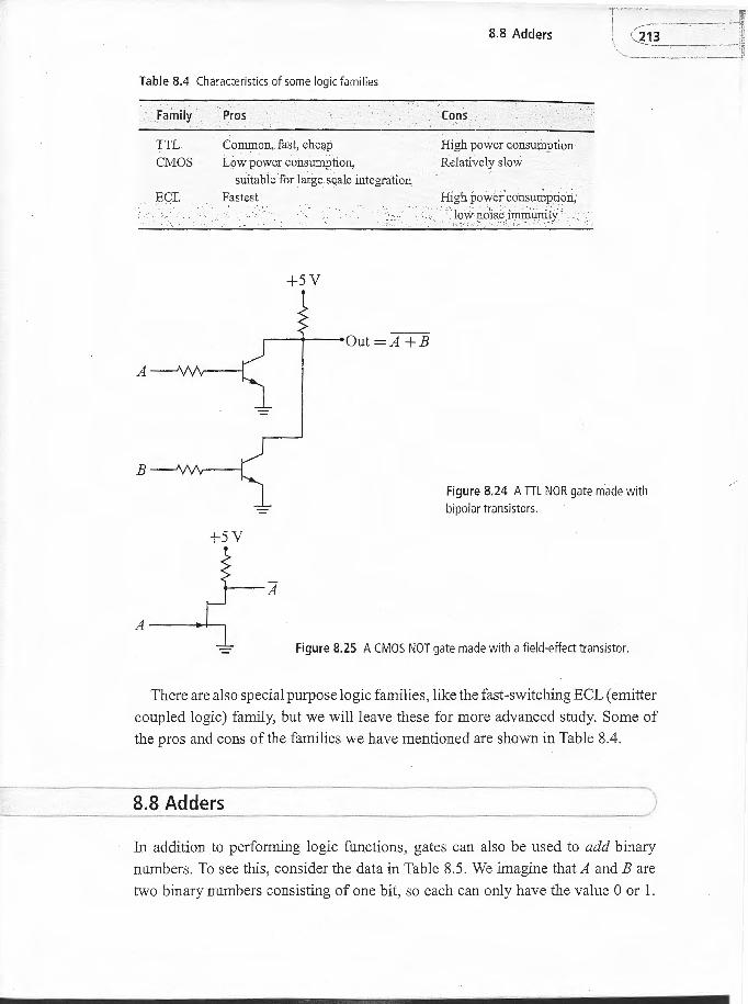
Semiconductor logic gates come in various types or families. One common type
is the transistor-transistor logic (or TTL) family. Here bipolar transistors are used
to create the logic gates. For example, the TTL NOR gate is shown in Fig. 8.24. If
either A nor B is high, its transistor is driven into saturation, making the collectoremitter voltage small and the gate output low. If neither A nor B is high, both
transistors are off, so there is no voltage drop across R and the output is high
(+5V). Another important logic family is the complementary metal oxide semiconductor
(or CMOS) family. These circuits employ field-effect transistors. For example, a
CMOS NOT gate is shown in Fig. 8.25 . When a high voltage is applied to the input
A, the transistor turns on and the voltage across it becomes small, thus giving a
low output. When a low voltage is applied, the transistor does not conduct, so the
output remains at +5 V (i.e. , high).
l f
I · 1
3te made l t ! l
logic is
gh.
ion type
ire used
8.24. If )Hector-
~h, both
is high
mductor
tmple, a
he input
giving a
:t, so the
Table 8.4 Characteristics of some logic families
A
B
Family
TTL CMOS
ECL
Pros
Common, fast, cheap
Low power consumption,
suitable for large scale integration
Fastest
+sv
.------1--0ut = A + B
+sv
8.8 Adders
Cons
High power consumption Relatively slow
High power consumption,
low noise immunity
Figure 8.24 A TTL NOR gate made with bipolar transistors.
Figure 8.25 A CMOS NOT gate made with a fie ld-effect transistor.
There are also special purpose logic families, like the fast-switching ECL (emitter
coupled logic) family, but we will leave these for more advanced study. Some of
the pros and cons of the families we have mentioned are shown in Table 8.4.
8.8 Adders
In addition to performing logic functions, gates can also be used to add binary
numbers. To see this, consider the data in Table 8.5. We imagine that A and Bare
two binary numbers consisting of one bit, so each can only have the value 0 or 1.