8-bit microcontroller mb89480/480l … contents chapter 1 overview 1 1.1 features of mb89480/480l...
TRANSCRIPT

FUJITSU SEMICONDUCTORCONTROLLER MANUAL
F2MC-8L8-BIT MICROCONTROLLER
MB89480/480L SeriesHARDWARE MANUAL
CM25-10151-2E

FUJITSU LIMITED
F2MC-8L8-BIT MICROCONTROLLER
MB89480/480L SeriesHARDWARE MANUAL
“Check Sheet” is seen at the following support page
URL : http://www.fujitsu.com/global/services/microelectronics/product/micom/support/index.html
“Check Sheet” lists the minimal requirement items to be checked to prevent problems beforehand in system development.
Be sure to refer to the “Check Sheet” for the latest cautions on development.

PREFACE
Objective and Intended Readership of This ManualThank you very much for your continued patronage of Fujitsu semiconductor products.
The MB89480/480L series has been developed as a general-purpose version of the F2MC-8L family
consisting of proprietary 8-bit, single-chip microcontrollers applicable as application-specific integrated
circuits (ASICs). The MB89480/480L series is applicable to a wide range of applications from welfare
products to industrial equipment, including portable devices.
This manual describes the functions and operation of the MB89480/480L series and is aimed at engineers
using the MB89480/480L series of microcontrollers to develop actual products. See "F2MC-8L MB89600
Series Programming Manual" for details on the MB89480/480L instruction set.
Note: F2MC is the abbreviation of FUJITSU Flexible Microcontroller.
Trademark
Embedded AlgorithmTM is a trademark of Advanced Micro Devices, Inc.
The company names and brand names herein are the trademarks or registered trademarks of their respective
owners.
Configuration of This ManualThis manual consists of the following 17 chapters and an appendix:
CHAPTER 1 OVERVIEW
Provides an overview of the features and functions of the MB89480/480L series.
CHAPTER 2 HANDLING DEVICES
Describes points to note when using the MB89480/480L series.
CHAPTER 3 CPU
Describes the functions of the MB89480/480L series CPU.
CHAPTER 4 I/O PORTS
Describes the function and operation of the MB89480/480L series I/O ports.
CHAPTER 5 TIME-BASE TIMER
Describes the function and operation of the MB89480/480L series time-base timer.
CHAPTER 6 WATCHDOG TIMER
Describes the functions and operation of the MB89480/480L series watchdog timer.
CHAPTER 7 WATCH PRESCALER
Describes the functions and operation of the MB89480/480L series watch prescaler.
CHAPTER 8 8-BIT PWM TIMER
Describes the functions and operation of the MB89480/480L series PWM timer.
CHAPTER 9 PWC TIMER
Describes the functions and operation of the MB90370 series PWC timer.
CHAPTER 10 6-BIT PPG TIMER
Describes the functions and operation of the MB89480/480L series 6-bit PPG.
i
CHAPTER 11 8/16-BIT TIMER/COUNTER
Describes the functions and operation of the MB89480/480L series 8/16-bit Timer/Counter.
CHAPTER 12 EXTERNAL INTERRUPT 1 CIRCUIT (EDGE)
Describes the function and operation of the MB89480/480L series external interrupt (edge).
CHAPTER 13 EXTERNAL INTERRUPT 2 CIRCUIT (LEVEL)
Describes the function and operation of the MB89480/480L series external interrupt (level).
CHAPTER 14 A/D CONVERTER
Describes the functions and operation of the MB89480/480L series A/D converter.
CHAPTER 15 UART/SIO
Describes the function and operation of the MB89480/480L series UART/SIO.
CHAPTER 16 BUZZER OUTPUT
Describes the function and operation of the MB89480/480L series audible alarm output.
CHAPTER 17 LCD CONTROLLER/DRIVER
Describes the function and operation of the MB89480/480L series liquid crystal display (LCD)
controller-driver circuit.
APPENDIX
The appendixes provide I/O maps, mask options, instruction summary, instruction list, instruction map
and other information.
ii
Copyright© 2004-2007 FUJITSU LIMITED All rights reserved
• The contents of this document are subject to change without notice.
Customers are advised to consult with FUJITSU sales representatives before ordering.
• The information, such as descriptions of function and application circuit examples, in this document are presented
solely for the purpose of reference to show examples of operations and uses of Fujitsu semiconductor device;
Fujitsu does not warrant proper operation of the device with respect to use based on such information. When you
develop equipment incorporating the device based on such information, you must assume any responsibility arising
out of such use of the information. Fujitsu assumes no liability for any damages whatsoever arising out of the use
of the information.
• Any information in this document, including descriptions of function and schematic diagrams, shall not be
construed as license of the use or exercise of any intellectual property right, such as patent right or copyright, or
any other right of Fujitsu or any third party or does Fujitsu warrant non-infringement of any third-party' s
intellectual property right or other right by using such information. Fujitsu assumes no liability for any
infringement of the intellectual property rights or other rights of third parties which would result from the use of
information contained herein.
• The products described in this document are designed, developed and manufactured as contemplated for general
use, including without limitation, ordinary industrial use, general office use, personal use, and household use, but
are not designed, developed and manufactured as contemplated (1) for use accompanying fatal risks or dangers
that, unless extremely high safety is secured, could have a serious effect to the public, and could lead directly to
death, personal injury, severe physical damage or other loss (i.e., nuclear reaction control in nuclear facility,
aircraft flight control, air traffic control, mass transport control, medical life support system, missile launch control
in weapon system), or (2) for use requiring extremely high reliability (i.e., submersible repeater and artificial
satellite).
Please note that Fujitsu will not be liable against you and/or any third party for any claims or damages arising in
connection with above-mentioned uses of the products.
• Any semiconductor devices have an inherent chance of failure. You must protect against injury, damage or loss
from such failures by incorporating safety design measures into your facility and equipment such as redundancy,
fire protection, and prevention of over-current levels and other abnormal operating conditions.
• If any products described in this document represent goods or technologies subject to certain restrictions on export
under the Foreign Exchange and Foreign Trade Law of Japan, the prior authorization by Japanese government will
be required for export of those products from Japan.
iii

READING THIS MANUAL
Page LayoutIn this manual, an entire section is presented on a single page or spread whenever possible.
The reader can thus view a section without having to flip pages.
The content of each section is summarized immediately below the title. You can obtain a rough overview
of this product by reading through these summaries.
Also, higher level section headings are given in lower sections so that you can know to which section the
text you are currently reading belongs.
Finding InformationIn addition to the standard table of contents and index, the following methods are available to find
information in a particular section when required.
Register index
Information can be looked up in the register index by register name, by bit name, and by their respective
abbreviations.
Subheading index
The sub-headings in each section (lines that start with ) are collected together in the subheading index.
The subheading index provides a means of looking up information at a finer level of detail than the table of
contents.
Naming Conventions for Register Name and Pin Name
Example for description of register name and bit name
By writing “1” to the sleep bit (STBC: SLP) in the standby control register.
Disable the interrupt request output (TBTC: TBIE = 0) from the time-base timer.
Interrupt is accepted if the interrupt is enabled (CCR: I = 1).
Notations for shared pins
Pin P14/SEG27/AN0
Many of the pins in the devices of this series are multi-function pins. (They can be switched between two
or more functions under program control.) The multiple names of these pins (indicating their multiple
functions) are separated by slant bars (/).
Bit nameRegister name abbreviation
Bit name abbreviation Register name
Bit name abbreviationSetup data
Register name abbreviation
Register name abbreviation
Bit name abbreviationCurrent status
iv

Facing Pages Organization and Notation Conventions
Subheading
Section summary Section title
Higher level sectionTable title
Figure title
Chapter title Series title
CheckPoints requiring check and prohibited items. Always read checks.
NoteProvides useful information for reference.
ReferenceIndicates an item ormanual that should be referenced.
v

Development Tools and Other Resources Required for Development
The following items are required for developing the MB89480/480L series.
Contact FUJITSU sales representative for the required development tools and other resources.
Manuals required for development
Checklist
• F2MC-8L MB89480/480L Series Data Sheet
(Provides electrical characteristics and various characteristic examples for the device.)
• F2MC-8L MB89600 Series Programming Manual
(Describes the F2MC-8L family instruction set.)
*• F2MC-8L MB89600 Series C Compiler Manual
(Only required when developing in C.)
(Describes program development in C and how to run the compiler.)
*• F2MC-8L MB89600 Series Assembler Manual
(Describes program development in assembly language.)
*• F2MC-8L MB89600 Series Support System Manual
(Describes how to run the macro assembler, linker, and library manager.)
*• F2MC-8L MB89600 Series Software Simulator Manual
(Only required when performing evaluation using the simulator.)
(Describes how to operate the software simulator.)
Manuals marked with * are provided with the products.
In addition, manuals for products such as development tools are provided with the product.
Software required for development
Checklist
• C compiler (Only required when developing in C.)
• Assembler, linker, librarian
• Software simulator (Only required when performing evaluation using the simulator.)
• Emulator/debugger (Only required when performing evaluation using the MB2140A series.)
The part number for each software package differs depending on the operating system.
See the F2MC development tools catalog or product guide for details.
Items required for evaluation using one-time PROM microcontrollers (when performing your own PROM
programming)
Checklist
• MB89P485
• ROM programmer (a programmer able to program an MBM27C256A)
See the data sheet for details of recommended programmers.
vi

Development tool
Checklist
• MB89PV480 (Piggyback/evaluation device)
• Evaluation tools
Check with the supplier when using a third party development environment.
Reference material
• F2MC development tools catalog
• Microcomputer product guide
(Main unit) (Pod) (Probe)
MB2141A + MB2144-505 + MB2144-202
vii

viii

CONTENTS
CHAPTER 1 OVERVIEW ................................................................................................... 11.1 Features of MB89480/480L Series ..................................................................................................... 21.2 MB89480/480L Series Product Range ............................................................................................... 41.3 Differences between Products ............................................................................................................ 71.4 Block Diagram of MB89480/480L Series ............................................................................................ 81.5 Pin Assignment ................................................................................................................................... 91.6 Package Dimensions ........................................................................................................................ 121.7 Pin Functions .................................................................................................................................... 16
CHAPTER 2 HANDLING DEVICES ................................................................................ 232.1 Notes on Handling Devices .............................................................................................................. 24
CHAPTER 3 CPU ............................................................................................................ 253.1 Memory Space .................................................................................................................................. 26
3.1.1 Special Purpose Areas ................................................................................................................ 283.1.2 Storing 16-bit Data in Memory ..................................................................................................... 30
3.2 Dedicated Registers ......................................................................................................................... 313.2.1 Condition Code Register (CCR) .................................................................................................. 333.2.2 Register Bank Pointer (RP) ......................................................................................................... 36
3.3 General-purpose Registers ............................................................................................................... 373.4 Interrupts ........................................................................................................................................... 39
3.4.1 Interrupt Level Setting Registers (ILR1, ILR2, ILR3, ILR4) ......................................................... 403.4.2 Interrupt Processing .................................................................................................................... 423.4.3 Multiple Interrupts ........................................................................................................................ 453.4.4 Interrupt Processing Time ........................................................................................................... 463.4.5 Stack Operation during Interrupt Processing ............................................................................... 473.4.6 Stack Area for Interrupt Processing ............................................................................................. 48
3.5 Resets ............................................................................................................................................... 493.5.1 Reset Flag Register (RSFR) ........................................................................................................ 513.5.2 External Reset Pin ....................................................................................................................... 533.5.3 Reset Operation .......................................................................................................................... 543.5.4 Pin States during Reset ............................................................................................................... 57
3.6 Clocks ............................................................................................................................................... 583.6.1 Clock Generator .......................................................................................................................... 603.6.2 Clock Controller ........................................................................................................................... 613.6.3 System Clock Control Register (SYCC) ...................................................................................... 633.6.4 Clock Modes ................................................................................................................................ 653.6.5 Oscillation Stabilization Wait Time .............................................................................................. 68
3.7 Standby Modes (Low-Power Consumption) ..................................................................................... 713.7.1 Operating States in Standby Modes ............................................................................................ 733.7.2 Sleep Mode ................................................................................................................................. 743.7.3 Stop Mode ................................................................................................................................... 753.7.4 Watch Mode ................................................................................................................................ 76
ix
3.7.5 Standby Control Register (STBC) ............................................................................................... 773.7.6 State Transition Diagram ............................................................................................................. 793.7.7 Notes on Using Standby Modes .................................................................................................. 81
3.8 Memory Access Mode ...................................................................................................................... 83
CHAPTER 4 I/O PORTS .................................................................................................. 854.1 Overview of I/O Ports ........................................................................................................................ 864.2 Port 0 ................................................................................................................................................ 88
4.2.1 Port 0 Registers (PDR0, DDR0, RDR0) ...................................................................................... 904.2.2 Operation of Port 0 ...................................................................................................................... 92
4.3 Port 1 ................................................................................................................................................ 944.3.1 Port 1 Registers (PDR1, DDR1) .................................................................................................. 964.3.2 Operation of Port 1 ...................................................................................................................... 98
4.4 Port 2 .............................................................................................................................................. 1004.4.1 Port 2 Registers (PDR2, DDR2, PURC2) .................................................................................. 1044.4.2 Operation of Port 2 .................................................................................................................... 106
4.5 Port 3 .............................................................................................................................................. 1084.5.1 Port 3 Register (PDR3) .............................................................................................................. 1104.5.2 Operation of Port 3 .................................................................................................................... 111
4.6 Port 4 .............................................................................................................................................. 1124.6.1 Port 4 Registers (PDR4) ............................................................................................................ 1144.6.2 Operation of Port 4 .................................................................................................................... 115
4.7 Port 5 .............................................................................................................................................. 1164.7.1 Port 5 Register (PDR5) .............................................................................................................. 1184.7.2 Operation of Port 5 .................................................................................................................... 119
4.8 Program Example for I/O Ports ....................................................................................................... 120
CHAPTER 5 TIME-BASE TIMER .................................................................................. 1215.1 Overview of Time-base Timer ......................................................................................................... 1225.2 Block Diagram of Time-base Timer ................................................................................................ 1245.3 Time-base Timer Control Register (TBTC) ..................................................................................... 1265.4 Time-base Timer Interrupt .............................................................................................................. 1285.5 Operation of Time-base Timer ........................................................................................................ 1295.6 Notes on Using Time-base Timer ................................................................................................... 1315.7 Program Example for Time-base Timer .......................................................................................... 133
CHAPTER 6 WATCHDOG TIMER ................................................................................ 1356.1 Overview of Watchdog Timer ......................................................................................................... 1366.2 Block Diagram of Watchdog Timer ................................................................................................. 1376.3 Watchdog Timer Control Register (WDTC) .................................................................................... 1396.4 Operation of Watchdog Timer ......................................................................................................... 1406.5 Notes on Using Watchdog Timer .................................................................................................... 1426.6 Program Example for Watchdog Timer .......................................................................................... 143
CHAPTER 7 WATCH PRESCALER ............................................................................. 1457.1 Overview of Watch Prescaler ......................................................................................................... 1467.2 Block Diagram of Watch Prescaler ................................................................................................. 148
x
7.3 Watch Prescaler Control Register (WPCR) .................................................................................... 1497.4 Watch Prescaler Interrupt ............................................................................................................... 1517.5 Operation of Watch Prescaler ......................................................................................................... 1527.6 Notes on Using Watch Prescaler .................................................................................................... 1547.7 Program Example for Watch Prescaler .......................................................................................... 156
CHAPTER 8 8-BIT PWM TIMER ................................................................................... 1578.1 Overview of 8-bit PWM Timer ......................................................................................................... 1588.2 Block Diagram of 8-bit PWM Timer ................................................................................................ 1608.3 Structure of 8-bit PWM Timer ......................................................................................................... 1628.4 Registers of 8-bit PWM Timer ......................................................................................................... 163
8.4.1 PWM Control Register (CNTR) ................................................................................................. 1648.4.2 PWM Compare Register (COMR) ............................................................................................. 166
8.5 8-bit PWM Timer Interrupts ............................................................................................................. 1688.6 Operation of Interval Timer Function .............................................................................................. 1698.7 Operation of PWM Timer Function ................................................................................................. 1708.8 States in Each Mode during 8-bit PWM Timer Operation ............................................................... 1718.9 Notes on Using 8-bit PWM Timer ................................................................................................... 1738.10 Program Example for 8-bit PWM Timer .......................................................................................... 174
CHAPTER 9 PWC TIMER ............................................................................................. 1779.1 Overview of Pulse Width Count Timer ............................................................................................ 1789.2 Block Diagram of Pulse Width Count Timer ................................................................................... 1809.3 Structure of Pulse Width Count Timer ............................................................................................ 1829.4 Registers of Pulse Width Count Timer ............................................................................................ 183
9.4.1 PWC Pulse Width Control Register 1 (PCR1) ........................................................................... 1849.4.2 PWC Pulse Width Control Register 2 (PCR2) ........................................................................... 1879.4.3 PWC Reload Buffer Register (PLBR) ........................................................................................ 189
9.5 Pulse Width Count Timer Interrupts ................................................................................................ 1919.6 Operation of Interval Timer Function .............................................................................................. 1929.7 Operation of Pulse Width Measurement Function .......................................................................... 1959.8 States in Each Mode during Pulse Width Count Timer Operation .................................................. 1989.9 Notes on Using Pulse Width Count Timer ...................................................................................... 1999.10 Program Example for Timer Function of Pulse Width Count Timer ................................................ 2009.11 Program Example for Pulse Width Measurement Function of Pulse Width Count Timer ............... 203
CHAPTER 10 6-BIT PPG TIMER .................................................................................... 20510.1 Overview of 6-bit PPG Timer .......................................................................................................... 20610.2 Block Diagram of 6-bit PPG Timer .................................................................................................. 20910.3 Pin of 6-bit PPG Timer .................................................................................................................... 21110.4 Registers of 6-bit PPG Timer .......................................................................................................... 212
10.4.1 6-bit PPG Control Register 1 (PPGC1) .................................................................................... 21310.4.2 6-bit PPG Control Register 2 (PPGC2) ..................................................................................... 214
10.5 Operation of 6-bit PPG Timer ......................................................................................................... 21510.6 Notes on Using 6-bit PPG Timer .................................................................................................... 21710.7 Program Example for 6-bit PPG Timer ........................................................................................... 219
xi

CHAPTER 11 8/16-BIT TIMER/COUNTER ..................................................................... 22111.1 Overview of 8/16-bit Timer/Counter ................................................................................................ 22211.2 Block Diagram of 8/16-bit Timer/Counter ....................................................................................... 22411.3 Pins of 8/16-bit Timer/Counter ........................................................................................................ 22611.4 Registers of 8/16-bit Timer/Counter ................................................................................................ 228
11.4.1 Timer 11/21 Control Register (T11CR/T21CR) ......................................................................... 22911.4.2 Timer 12/22 Control Register (T12CR/T22CR) ......................................................................... 23111.4.3 Timer 11/21 Data Register (T11DR/T21DR) ............................................................................. 23311.4.4 Timer 12/22 Data Register (T12DR/T22DR) ............................................................................. 235
11.5 8/16-bit Timer/Counter Interrupt ..................................................................................................... 23711.6 Operation of Interval Timer Function .............................................................................................. 23911.7 Operation of Counter Function ....................................................................................................... 24111.8 Operation of the Square Wave Output Initial Setting Function ....................................................... 24311.9 Operation of 8/16-bit Timer/Counter Stop and Restart ................................................................... 24511.10 States in Each Mode during 8/16-bit Timer/Counter Operation ...................................................... 24611.11 Notes on Using 8/16-bit Timer/Counter .......................................................................................... 24711.12 Program Examples for 8/16-bit Timer/Counter ............................................................................... 249
CHAPTER 12 EXTERNAL INTERRUPT 1 CIRCUIT (EDGE) ......................................... 25312.1 Overview of the External Interrupt 1 Circuit .................................................................................... 25412.2 Block Diagram of the External Interrupt 1 Circuit ............................................................................ 25512.3 Pins of the External Interrupt 1 Circuit ............................................................................................ 25612.4 Registers of External Interrupt 1 Circuit .......................................................................................... 257
12.4.1 External Interrupt Control Register 1 (EIC1) .............................................................................. 25812.4.2 External Interrupt Control Register 2 (EIC2) .............................................................................. 260
12.5 External Interrupt 1 Circuit Interrupts .............................................................................................. 26212.6 Operation of the External Interrupt 1 Circuit ................................................................................... 26312.7 Program Example for the External Interrupt 1 Circuit ..................................................................... 264
CHAPTER 13 EXTERNAL INTERRUPT 2 CIRCUIT (LEVEL) ....................................... 26513.1 Overview of External Interrupt 2 Circuit (Level) .............................................................................. 26613.2 Block Diagram of External Interrupt 2 Circuit .................................................................................. 26713.3 Pins of External Interrupt 2 Circuit .................................................................................................. 26813.4 Registers of External Interrupt 2 Circuit .......................................................................................... 270
13.4.1 External Interrupt 2 Control Register (EIE2) .............................................................................. 27113.4.2 External Interrupt 2 Flag Register (EIF2) ................................................................................... 273
13.5 External Interrupt 2 Circuit Interrupt ................................................................................................ 27413.6 Operation of External Interrupt 2 Circuit ......................................................................................... 27513.7 Program Example for External Interrupt 2 Circuit ........................................................................... 276
CHAPTER 14 A/D CONVERTER .................................................................................... 27714.1 Overview of A/D Converter ............................................................................................................. 27814.2 Block Diagram of A/D Converter ..................................................................................................... 27914.3 Pins of A/D Converter ..................................................................................................................... 28114.4 Registers of A/D Converter ............................................................................................................. 282
14.4.1 A/D Control Register 1 (ADC1) .................................................................................................. 28314.4.2 A/D Control Register 2 (ADC2) .................................................................................................. 285
xii

14.4.3 A/D Data Registers (ADDL and ADDH) ..................................................................................... 28714.5 A/D Converter Interrupt ................................................................................................................... 28814.6 Operation of A/D Converter ............................................................................................................ 28914.7 Notes on Using A/D Converter ....................................................................................................... 29114.8 Program Example for A/D Converter .............................................................................................. 293
CHAPTER 15 UART/SIO ................................................................................................. 29515.1 Overview of UART/SIO ................................................................................................................... 29615.2 Block Diagram of UART/SIO .......................................................................................................... 29715.3 Pins of UART/SIO ........................................................................................................................... 29915.4 Registers of UART/SIO ................................................................................................................... 301
15.4.1 Serial Mode Control Register 1 (SMC1) .................................................................................... 30215.4.2 Serial Mode Control Register 2 (SMC2) .................................................................................... 30415.4.3 Serial Status and Data Register (SSD) ..................................................................................... 30615.4.4 Serial Input Data Register (SIDR) ............................................................................................. 30815.4.5 Serial Output Data Register (SODR) ......................................................................................... 30915.4.6 Serial Rate Control Register (SRC) ........................................................................................... 310
15.5 UART/SIO Interrupts ....................................................................................................................... 31115.6 Operation of UART/SIO .................................................................................................................. 31215.7 Operation of mode 0 ....................................................................................................................... 31315.8 Operation of mode 1 ....................................................................................................................... 317
CHAPTER 16 BUZZER OUTPUT .................................................................................... 32316.1 Overview of Buzzer Output ............................................................................................................. 32416.2 Block Diagram of Buzzer Output .................................................................................................... 32616.3 Structure of Buzzer Output ............................................................................................................. 327
16.3.1 Buzzer Register (BUZR) ............................................................................................................ 32816.4 Program Example for Buzzer Output .............................................................................................. 329
CHAPTER 17 LCD CONTROLLER/DRIVER .................................................................. 33117.1 Overview of LCD Controller/Driver ................................................................................................. 33217.2 Block Diagram of LCD Controller/Driver ......................................................................................... 333
17.2.1 LCD Controller/Driver Internal Dividing Resistors (Device without Voltage Booster) ................ 33517.2.2 LCD Controller/Driver External Dividing Resistors (Device without Booster) ............................ 33817.2.3 LCD Controller/Driver Power Supply Voltage (Devices with Internal Voltage Booster) ............. 339
17.3 Structure of LCD Controller/Driver .................................................................................................. 34117.3.1 LCD Controller Register (LCR1) ................................................................................................ 34717.3.2 LCD Controller Register 2 (LCR2) ............................................................................................. 34917.3.3 Display RAM .............................................................................................................................. 351
17.4 Operation of LCD Controller/Driver ................................................................................................. 35317.4.1 Output Waveforms during LCD controller/Driver Operation (1/2 Duty Ratio) ............................ 35517.4.2 Output Waveforms during LCD Controller/Driver Operation (1/3 Duty Ratio) ........................... 35817.4.3 Output Waveforms during LCD Controller/Driver Operation (1/4 Duty Ratio) ........................... 361
17.5 Program Example for LCD Controller/Driver .................................................................................. 364
xiii
APPENDIX ......................................................................................................................... 367APPENDIX A I/O MAP ............................................................................................................................. 368APPENDIX B Instructions ........................................................................................................................ 371
B.1 Addressing ..................................................................................................................................... 373B.2 Special Instructions ........................................................................................................................ 377B.3 F2MC-8L Instructions ..................................................................................................................... 381B.4 Instruction Map ............................................................................................................................... 386B.5 Bit Manipulation Instructions (SETB, CLRB) .................................................................................. 387
APPENDIX C Mask Options ..................................................................................................................... 388APPENDIX D Programming Specifications for one-time PROM and EPROM Microcontrollers .............. 389
D.1 Programming One-time PROM Microcontroller with serial programmer ........................................ 390D.2 Programming One-time PROM Microcontroller parallel programmer ............................................ 391D.3 Programming EPROM for Piggyback/Evaluation Device ............................................................... 392
APPENDIX E MB89480/480L Series Pin States ...................................................................................... 393
INDEX................................................................................................................................... 395
xiv

Main changes in this edition
The vertical lines marked in the left side of the page show the changes.
Page Changes (For details, refer to main body.)
-Changed the terms(Port data direction register → Port direction register)
8Figure 1.4-1 Block Diagram of MB89480/480L Series is changed.(Changed the arrow directions of X1, X1A)
49 Note is added.
60 Note is deleted.
87Table 4.1-1 Port Functions is changed.(The line of Port5 is added.)
187Figure 9.4-3 PWC Pulse Width Control Register 2 (PCR2)Measured pulses are changed for the W2, W1, W0=110.(High level and rising to rising → Both edges)
334
Display RAM is changed.(Its contents are automatically read out to the segment outputs in sync with the timing of the selected common signal. → Its contents are automatically read in sync with the timing of the selected common signal, and output from the segment outputs at the same time as writing the display RAM.)
385Table B.3-4 Other Instructions is changed.(The instructions are added in operation.)
388 Note is added.
xv

xvi
CHAPTER 1OVERVIEW
This chapter describes the features and basic specifications of the MB89480/480L series.
1.1 Features of MB89480/480L Series
1.2 MB89480/480L Series Product Range
1.3 Differences between Products
1.4 Block Diagram of MB89480/480L Series
1.5 Pin Assignment
1.6 Package Dimensions
1.7 Pin Functions
1

CHAPTER 1 OVERVIEW
1.1 Features of MB89480/480L Series
The MB89480/480L series has been developed as a general-purpose version of the
F2MC-8L family consisting of 8-bit proprietary, single-chip microcontrollers.In addition to a compact instruction set, the microcontrollers contain a variety of peripheral functions such as 21-bit time-base timer, watch prescaler, PWC timer, PWM timer, 8/16-bit timer/counter, 6-bit PPG, LCD controller/driver, external interrupt 1 (edge), external interrupt 2 (level), 10-bit A/D converter, UART/SIO, buzzer, watchdog timer reset.The MB89480/480L series is designed suitable for LCD remote controller as well as in a wide range of applications for consumer product.
Features of MB89480/480L Series• Supports high speed operation
Minimum instruction execution time: 0.32µs (source oscillation at 12.5MHz)
• Package used
QFP package and SH-DIP package for MB89P485/L, MB89485/L
MDIP package and MQFP package for MB89PV480
• F2MC-8L CPU core
Instructions set optimized for controller applications
- Multiplication and division instructions
- 16-bit operations
- Bit-test branch instructions
- Bit manipulation instructions, etc.
• Six timers sub-systems
- PWC timer (also usable as an interval timer)
- PWM timer
- 8/16-bit timer/counter 2 ch
- 21-bit time-base timer
- Watch prescaler
• Programmable Pulse Generator (PPG)
- 6-bit PPG with program -selectable pulse width and period
• External interrupts
- Edge detection (Selectable edge) : 4 channels
- "L" level interrupt (Wake-up function): 8 channels
• A/D converter (4 channels)
- 10-bit successive approximation type
• UART / SIO
- Synchronous/asynchronous data transfer capable
2

• LCD controller/driver
- max. 31 segments output × 4 commons
- Booster for LCD driving (selected by mask option)
• Buzzer
- 7 frequency types are selectable by software
• Low-power consumption modes
- Stop mode (Oscillation stops to minimize the current dissipation.)
- Sleep mode (The CPU stops to reduce the current dissipation to approx. 1/3 of normal.)
- Watch mode (Operation except the watch prescaler stops to reduce the power dissipation to an
extremely low level.)
- Sub clock mode
• Watchdog timer reset
• I/O ports
- Max 42 channels
3
CHAPTER 1 OVERVIEW
1.2 MB89480/480L Series Product Range
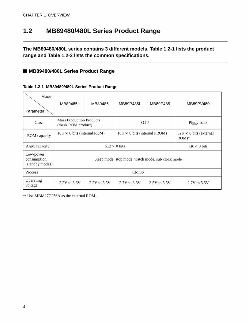
The MB89480/480L series contains 3 different models. Table 1.2-1 lists the product range and Table 1.2-2 lists the common specifications.
MB89480/480L Series Product Range
*: Use MBM27C256A as the external ROM.
Table 1.2-1 MB89480/480L Series Product Range
Model
Parameter
MB89485L MB89485 MB89P485L MB89P485 MB89PV480
ClassMass Production Products(mask ROM product)
OTP Piggy-back
ROM capacity16K × 8 bits (internal ROM) 16K × 8 bits (internal PROM) 32K × 8 bits (external
ROM)*
RAM capacity 512 × 8 bits 1K × 8 bits
Low-power consumption (standby modes)
Sleep mode, stop mode, watch mode, sub clock mode
Process CMOS
Operating voltage
2.2V to 3.6V 2.2V to 5.5V 2.7V to 3.6V 3.5V to 5.5V 2.7V to 5.5V
4

Table 1.2-2 Common Specifications for the MB89480/480L Series (1 / 2)
Parameter Specification
CPU functions
Number of instructionsInstruction bit lengthInstruction lengthData bit lengthMinimum instruction execution time Minimum interrupt processing time
: 136 instructions: 8-bit: 1 to 3 bytes: 1, 8, or 16-bit: 0.32µs/12.5 MHz: 2.88µs/12.5 MHz
Per
iphe
ral f
unct
ions
Ports
I/O ports (CMOS)N-channel open drain I/O portsOutput ports (N-channel open drain)Input portTotal
: 11 pins: 28 pins: 2 pins: 1 pins: 42 pins
Time-base timer21-bitInterrupt period (0.66ms, 2.6 ms, 21.0 ms, 335.5 ms) at 12.5 MHz
Watchdog timer Reset period (167.8 ms to 335.5 ms) at 12.5 MHz
Pulse width count timer
1 channel8-bit one-shot timer operation (supports underflow output, operating clock period: 1, 4, 32 tinst, external)8-bit reload timer operation (supports square wave output, operating clock period: 1, 4, 32 tinst, external)8-bit pulse width measurement operation (supports continuous measurement, H width, L width, rising edge to rising edge, falling edge to falling edge measurement and both edge measurement)
PWM timer8-bit reload timer operation (supports square wave output, operating clock period: 1, 8, 16, 64 tinst)8-bit resolution PWM operation
6-bit programmable pulse generator
Can generate square wave with programmable period.
8/16-bit timer/counter 11, 12
Can be operated either as a 2-channel 8-bit timer/counter (Timer 11 and Timer 12, each with its own independent operating clock cycle), or as one 16-bit timer/counterIn Timer 11 or 16-bit timer/counter operation, event counter operation (external clock-triggered) and square wave output capable
8/16-bit timer/counter 21, 22
Can be operated either as a 2-channel 8-bit timer/counter (Timer 21 and Timer 22, each with its own independent operating clock cycle), or as one 16-bit timer/counterIn Timer 21 or 16-bit timer/counter operation, event counter operation (external clock-triggered) and square wave output capable
External Interrupt
4 independent channels (selectable edge, interrupt vector, request flag)8 channels ("L" level interrupt)
5

CHAPTER 1 OVERVIEW
*: tinst is instruction cycle (execution time) which can be selected as 1/4, 1/8, 1/16, or 1/64 of main clock. See "3.6.3 System
Clock Control Register (SYCC)".
Per
iphe
ral f
unct
ions
A/D converter10-bit resolution × 4 channelsA/D conversion function (conversion time: 60 tinst)Supports repeated activation by internal clock.
LCD controller/driver
Common outputSegment outputBias power supply pinsLCD display RAM sizeInternal dividing resistor ladder/booster
: 4 (max.): 31 (max.) (Select resistor ladder) /26 (max.) (Select booster): 4: 31 x 4 bits: selected by mask option
UART/SIOSynchronous/asynchronous data transfer capable (7 and 8 bits with parity bit; 8 and 9 bits without parity bit)
Buzzer output 7 frequency types are selectable by software
Low-power consumption modes
Sleep mode, stop mode, watch mode, sub clock mode
Process CMOS
Table 1.2-2 Common Specifications for the MB89480/480L Series (2 / 2)
Parameter Specification
6
1.3 Differences between Products
This section describes the differences between the 5 products in the MB89480/480L series and lists points to note in products selection.
Differences between Products and Points to Note for Product Selection
• Memory space
Before evaluating using the piggyback product, verify its differences from the product that will actually
be used. Take particular care on the following points:
- The stack area, etc., is set at the upper limit of the RAM.
• Current dissipation
- For the MB89PV480, add the current consumed by the EPROM mounted in the piggyback socket.
- When operating at low speed, the current consumed by the one-time PROM products is greater than
that for the mask ROM product. However, the current dissipation are roughly the same in sleep or
stop mode.
Reference:
See " Electrical characteristics" in the data sheet for details.
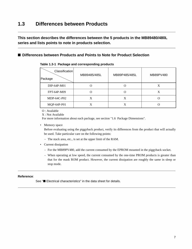
Table 1.3-1 Package and corresponding products
Classification
PackageMB89485/485L MB89P485/485L MB89PV480
DIP-64P-M01 O O X
FPT-64P-M09 O O X
MDP-64C-P02 X X O
MQP-64P-P01 X X O
O : AvailableX : Not AvailableFor more information about each package, see section "1.6 Package Dimensions".
7

CHAPTER 1 OVERVIEW
1.4 Block Diagram of MB89480/480L Series
The block diagram of MB89480/480L series is shown in Figure 1.4-1.
Block Diagram of MB89480/480L Series
Figure 1.4-1 Block Diagram of MB89480/480L Series
Main clock
Clock control
Sub-clock
RAM (512 bytes/1 Kbyte)
F2MC-8LCPU
ROM (16 Kbytes/32 Kbyte)
Other pinsVcc, Vss, MODE, C *2
Inte
rnal
dat
a bu
s
21-bit time-base
UART/SIOP
ort 0
Por
t 1
X0X1
P07/INT27/BUZ
P21/SCKP22/SOP23/SI
timer
X0AX1A
Por
t 3
N-ch open-drain output port
2
Buzzer output
4
LCD controller/driver
32 × 4-bit display RAM (16 bytes)
8-bit PWM timer
Por
t 4 a
nd P
ort 5
*4
N-ch open-drain I/O port
P10/SEG23/INT10 to
P13/SEG26/INT13
SEG1 to SEG77
COM0 toCOM1
2
V3V0/SEG0 *3
8
P30/COM2
P31/COM3
Reset circuit(Watchdog timer)RST
External interrupt 1(edge)
4
4
16 P56/SEG22 to P54/SEG20
oscillator
oscillator
Watch prescaler
8/16-bit timer/counter 21,22
CMOS I/O port *4
Por
t 2 *
4
8/16-bit timer/counter 11,12
Booster
2
2
P20/PWM
P24/C1/TO2 *1
P25/C0/EC2 *1
P26/V1/TO1P27/V2/EC1
CMOS I/O port
External interrupt 2(level)
8
8-bitP05/INT25/PWCPWC timer
6-bit PPG P06/INT26/PPG
P04/INT24 *1
P02/INT22
P03/INT23 *1
to P00/INT20
10-bitA/D converter
P14/SEG27/AN0 *1
toP17/SEG30/AN3 *1
AVccAVss
4
*1: If booster is selected, EC2 and TO2 will be redirected to P03/INT23 and P04/INT24 respectively.Segment output of P14/SEG27/AN0 to P17/SEG30/AN3 will be disabled.
*2: For product other than MB89P485, C pin is N.C. pin.*3: If booster is selected, it serves as V0. If booster is not selected, it serves as SEG0.*4: P20 to P23 are CMOS I/O ports. P24 to P27 are N-ch open-drain I/O ports. P57 is input-only port.
N-ch open-drain I/O port
P57
3
P53/SEG19 to P50/SEG16
4
P47/SEG15 to P44/SEG12
4
P43/SEG11 to P40/SEG8
4
8
1.5 Pin Assignment
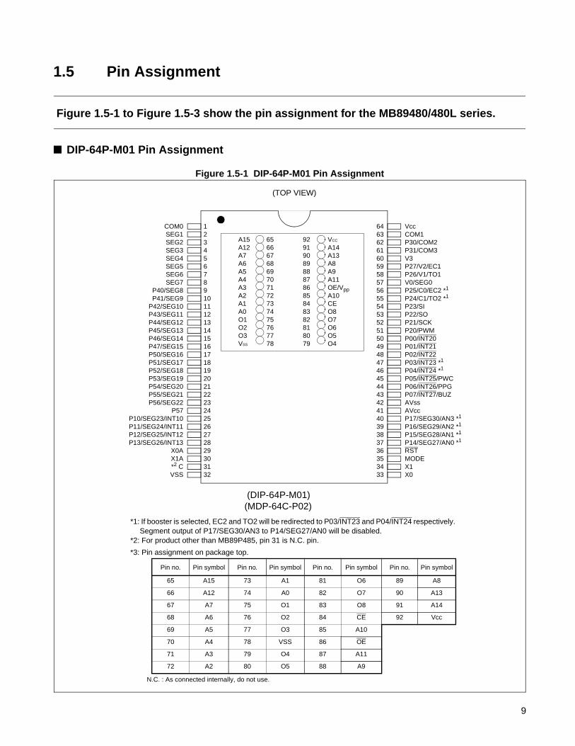
Figure 1.5-1 to Figure 1.5-3 show the pin assignment for the MB89480/480L series.
DIP-64P-M01 Pin Assignment
Figure 1.5-1 DIP-64P-M01 Pin Assignment
COM0SEG1SEG2SEG3SEG4SEG5SEG6SEG7
P40/SEG8P41/SEG9
P42/SEG10P43/SEG11P44/SEG12P45/SEG13P46/SEG14P47/SEG15P50/SEG16P51/SEG17P52/SEG18P53/SEG19P54/SEG20P55/SEG21P56/SEG22
P57P10/SEG23/INT10P11/SEG24/INT11P12/SEG25/INT12P13/SEG26/INT13
X0AX1A*2 CVSS
VccCOM1P30/COM2P31/COM3V3P27/V2/EC1P26/V1/TO1V0/SEG0P25/C0/EC2 *1
P24/C1/TO2 *1
P23/SIP22/SOP21/SCKP20/PWMP00/INT20P01/INT21P02/INT22P03/INT23 *1
P04/INT24 *1
P05/INT25/PWCP06/INT26/PPGP07/INT27/BUZAVssAVccP17/SEG30/AN3 *1
P16/SEG29/AN2 *1
P15/SEG28/AN1 *1
P14/SEG27/AN0 *1
RSTMODEX1X0
1234567891011121314151617181920212223242526272829303132
6463626160595857565554535251504948474645444342414039383736353433
(DIP-64P-M01)(MDP-64C-P02)
*1: If booster is selected, EC2 and TO2 will be redirected to P03/INT23 and P04/INT24 respectively.Segment output of P17/SEG30/AN3 to P14/SEG27/AN0 will be disabled.
*2: For product other than MB89P485, pin 31 is N.C. pin.
*3: Pin assignment on package top.
N.C. : As connected internally, do not use.
Pin no. Pin symbol Pin no. Pin symbol Pin no. Pin symbol Pin no. Pin symbol
65 A15 73 A1 81 O6 89 A8
66 A12 74 A0 82 O7 90 A13
67 A7 75 O1 83 O8 91 A14
68 A6 76 O2 84 CE 92 Vcc
69 A5 77 O3 85 A10
70 A4 78 VSS 86 OE
71 A3 79 O4 87 A11
72 A2 80 O5 88 A9
(TOP VIEW)
A15A12A7A6A5A4A3A2A1A0O1O2O3VSS
VCC
A14A13A8A9A11OE/VppA10CEO8O7O6O5O4
6566676869707172737475767778
9291908988878685848382818079
9
CHAPTER 1 OVERVIEW
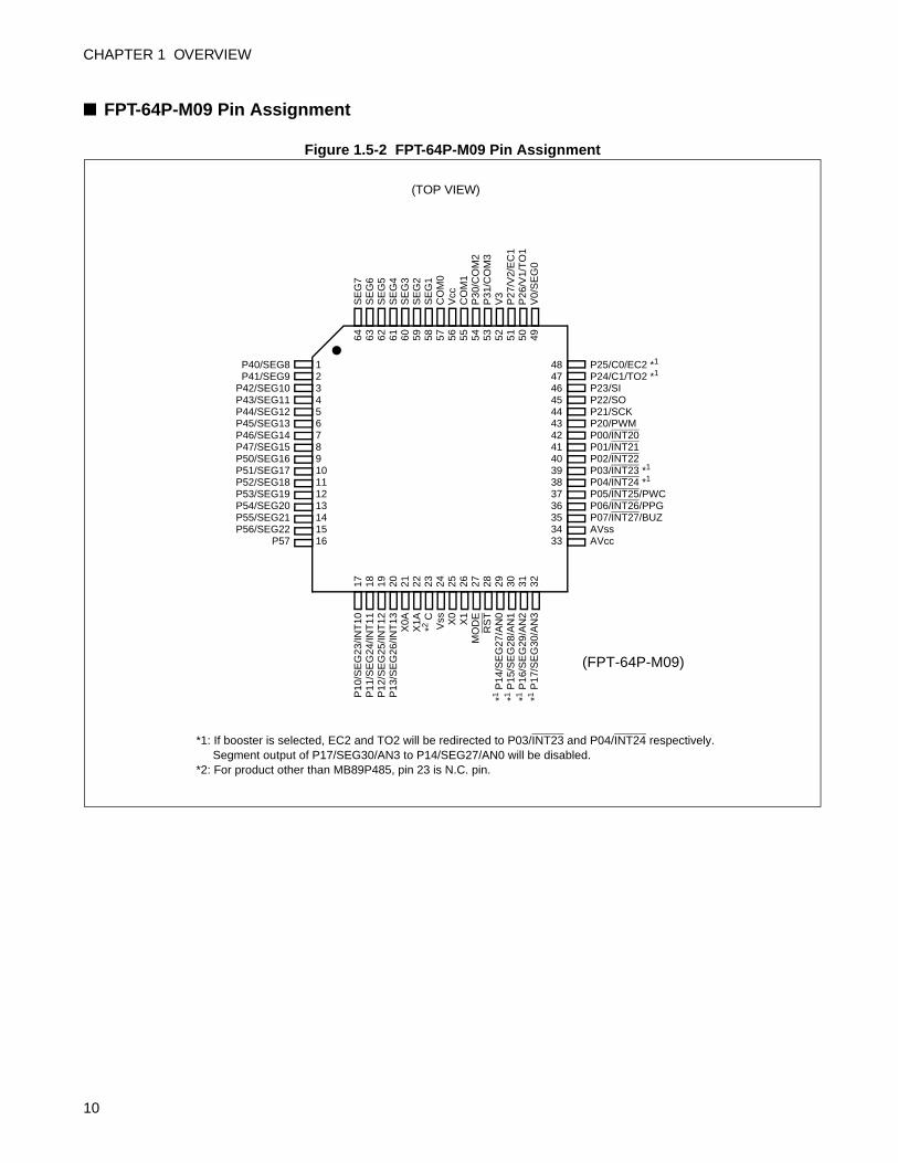
FPT-64P-M09 Pin Assignment
Figure 1.5-2 FPT-64P-M09 Pin Assignment
(FPT-64P-M09)
*1: If booster is selected, EC2 and TO2 will be redirected to P03/INT23 and P04/INT24 respectively.Segment output of P17/SEG30/AN3 to P14/SEG27/AN0 will be disabled.
*2: For product other than MB89P485, pin 23 is N.C. pin.
P40/SEG8P41/SEG9
P42/SEG10P43/SEG11P44/SEG12P45/SEG13P46/SEG14P47/SEG15P50/SEG16P51/SEG17P52/SEG18P53/SEG19P54/SEG20P55/SEG21P56/SEG22
P57
12345678910111213141516
P10
/SE
G23
/INT
10P
11/S
EG
24/IN
T11
P12
/SE
G25
/INT
12P
13/S
EG
26/IN
T13
X0A
X1A
*2 CV
ss X0
X1
MO
DE
RS
T*1 P
14/S
EG
27/A
N0
*1 P
15/S
EG
28/A
N1
*1 P
16/S
EG
29/A
N2
*1 P17
/SE
G30
/AN
3
17 18 19 20 21 22 23 24 25 26 27 28 29 30 31 32
P25/C0/EC2 *1
P24/C1/TO2 *1
P23/SIP22/SOP21/SCKP20/PWMP00/INT20P01/INT21P02/INT22P03/INT23 *1
P04/INT24 *1
P05/INT25/PWCP06/INT26/PPGP07/INT27/BUZAVssAVcc
48474645444342414039383736353433
SE
G7
SE
G6
SE
G5
SE
G4
SE
G3
SE
G2
SE
G1
CO
M0
Vcc
CO
M1
P30
/CO
M2
P31
/CO
M3
V3
P27
/V2/
EC
1P
26/V
1/T
O1
V0/
SE
G0
64 63 62 61 60 59 58 57 56 55 54 53 52 51 50 49
(TOP VIEW)
10

MQP-64C-P01 Pin Assignment
Figure 1.5-3 MQP-64C-P01 Pin Assignment
SEG7
P40/SEG8
P41/SEG9
P42/SEG10
P43/SEG11
P44/SEG12
P45/SEG13
P46/SEG14
P47/SEG15
P50/SEG16
P51/SEG17
P52/SEG18
P53/SEG19
P54/SEG20
P55/SEG21
P56/SEG22
P57
P10/SEG23/INT10
P11/SEG24/INT11
1
2
3
4
5
6
7
8
9
10
11
12
13
14
15
16
17
18
19
51
50
49
48
47
46
45
44
43
42
41
40
39
38
37
36
35
34
33
SE
G6
SE
G5
SE
G4
SE
G3
SE
G2
SE
G1
CO
M0
Vcc
CO
M1
P30
/CO
M2
P31
/CO
M3
V3
P27
/V2/
EC
1
64 63 62 61 60 59 58 57 56 55 54 53 52
P12
/SE
G25
/INT
12
P13
/SE
G26
/INT
13
X0A
X1A
*2 C
Vss X0
X1
MO
DE
RS
T
*1 P
14/S
EG
27/A
N0
*1 P
15/S
EG
28/A
N1
*1 P
16/S
EG
29/A
N2
20 21 22 23 24 25 26 27 28 29 30 31 32
858687888990919293
777675747372717069
94 95 96 65 66 67 68
84 83 82 81 80 79 78
(TOP VIEW)
(MQP-64C-P01)
*1: If booster is selected, EC2 and TO2 will be redirected to P03/INT23 and P04/INT24 respectively.Segment output of P17/SEG30/AN3 to P14/SEG27/AN0 will be disabled.
*2: Pin 24 is N.C. pin.
Pin assignment on package top
N.C.: As connected internally, do not use.
Pin No.
Pin Symbol
Pin No.
Pin Symbol
Pin No.Pin
SymbolPin No.
Pin Symbol
65 N.C. 73 A2 81 N.C. 89 OE
66 Vpp 74 A1 82 O4 90 N.C.
67 A12 75 A0 83 O5 91 A11
68 A7 76 N.C. 84 O6 92 A9
69 A6 77 O1 85 O7 93 A8
70 A5 78 O2 86 O8 94 A13
71 A4 79 O3 87 CE 95 A14
72 A3 80 VSS 88 A10 96 VCC
P26/V1/TO1
V0/SEG0
P25/C0/EC2 *1
P24/C1/TO2 *1
P23/SI
P22/SO
P21/SCK
P20/PWM
P00/INT20
P01/INT21
P02/INT22
P03/INT23 *1
P04/INT24 *1
P05/INT25/PWC
P06/INT26/PPG
P07/INT27/BUZ
AVss
AVcc
P17/SEG30/AN3 *1
11
CHAPTER 1 OVERVIEW
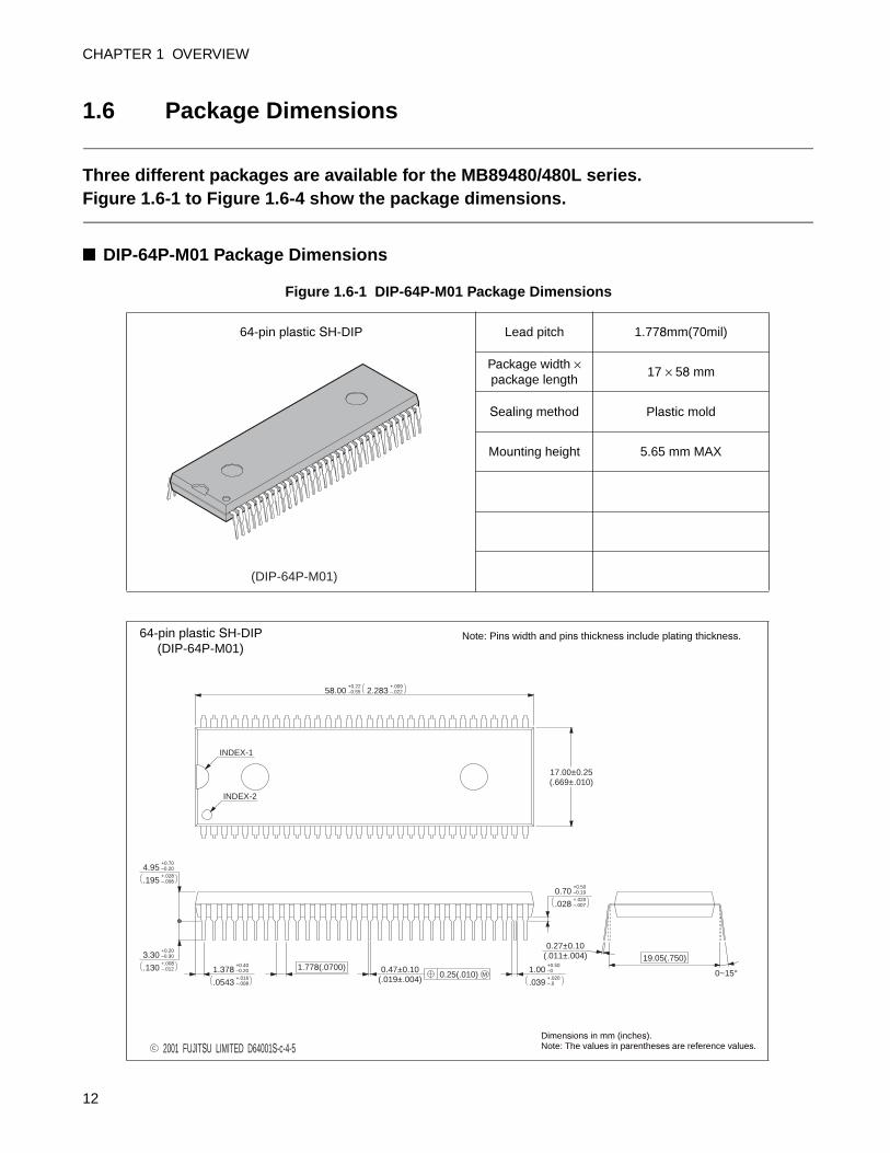
1.6 Package Dimensions
Three different packages are available for the MB89480/480L series. Figure 1.6-1 to Figure 1.6-4 show the package dimensions.
DIP-64P-M01 Package Dimensions
Figure 1.6-1 DIP-64P-M01 Package Dimensions
64-pin plastic SH-DIP Lead pitch 1.778mm(70mil)
Package width ×package length
17 × 58 mm
Sealing method Plastic mold
Mounting height 5.65 mm MAX
64-pin plastic SH-DIP(DIP-64P-M01)
(DIP-64P-M01)
C 2001 FUJITSU LIMITED D64001S-c-4-5
58.00+0.22–0.55
+.009–.0222.283
17.00±0.25(.669±.010)
3.30+0.20–0.30
.130 –.012+.008
+.028–.008.195
–0.20+0.70
4.95
+.016–.008.0543
–0.20+0.40
1.378 1.778(.0700) 0.47±0.10(.019±.004)
1.00+0.50–0
.039 –.0+.020
+.020–.007.028
–0.19+0.50
0.70
19.05(.750)(.011±.004)0.27±0.10
0~15°
INDEX-2
INDEX-1
M0.25(.010)
Note: Pins width and pins thickness include plating thickness.
Dimensions in mm (inches).Note: The values in parentheses are reference values.
12
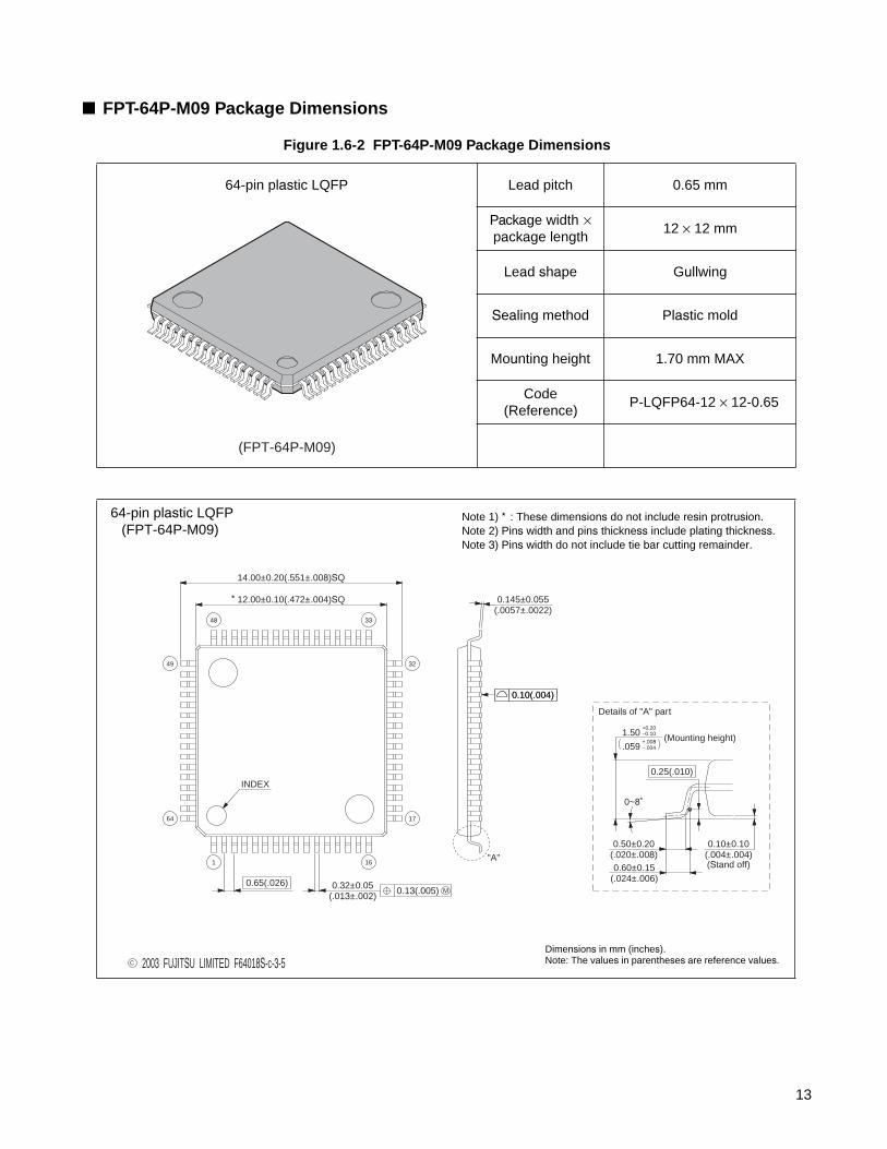
FPT-64P-M09 Package Dimensions
Figure 1.6-2 FPT-64P-M09 Package Dimensions
64-pin plastic LQFP Lead pitch 0.65 mm
Package width ×package length
12 × 12 mm
Lead shape Gullwing
Sealing method Plastic mold
Mounting height 1.70 mm MAX
Code(Reference)
P-LQFP64-12 × 12-0.65
64-pin plastic LQFP(FPT-64P-M09)
(FPT-64P-M09)
C 2003 FUJITSU LIMITED F64018S-c-3-5
0.65(.026)
0.10(.004)
1 16
17
3249
64
3348
12.00±0.10(.472±.004)SQ
14.00±0.20(.551±.008)SQ
INDEX
0.32±0.05(.013±.002)
M0.13(.005)
0.145±0.055(.0057±.0022)
"A"
.059 –.004+.008
–0.10+0.20
1.50
0~8˚
0.25(.010)
(Mounting height)
0.50±0.20(.020±.008)0.60±0.15
(.024±.006)
0.10±0.10(.004±.004)
Details of "A" part
(Stand off)
0.10(.004)
*
Dimensions in mm (inches).Note: The values in parentheses are reference values.
Note 1) * : These dimensions do not include resin protrusion.Note 2) Pins width and pins thickness include plating thickness.Note 3) Pins width do not include tie bar cutting remainder.
13

CHAPTER 1 OVERVIEW
MDP-64C-P02 Package Dimensions
Figure 1.6-3 MDP-64C-P02 Package Dimensions
64-pin ceramic MDIP Lead pitch 1.778mm (70mil)
15.24mm (750mm)
Motherboard material
Ceramic
Plastic mold
64-pin ceramic MDIP(MDP-64C-P02)
(MDP-64C-P02)
+0.13–0.08+.005–.003
INDEX AREA
0°~9°
(.750±.012)19.05±0.30
0.46
.018
(2.240±.025)
(.010±.002)0.25±0.05
(.050±.010)1.27±0.25
(.135±.015)3.43±0.38
55.12(2.170)REF
(.035±.005)0.90±0.13
(.070±.010)1.778±0.25
10.16(.400)MAX
33.02(1.300)REF(.100±.010)2.54±0.25
(.738±.012)18.75±0.30
TYP15.24(.600)
56.90±0.64
1994 FUJITSU LIMITED M64002SC-1-4C
Dimensions in mm (inches).Note: The values in parentheses are reference values.
Row spacing
Mountedpacking material
14
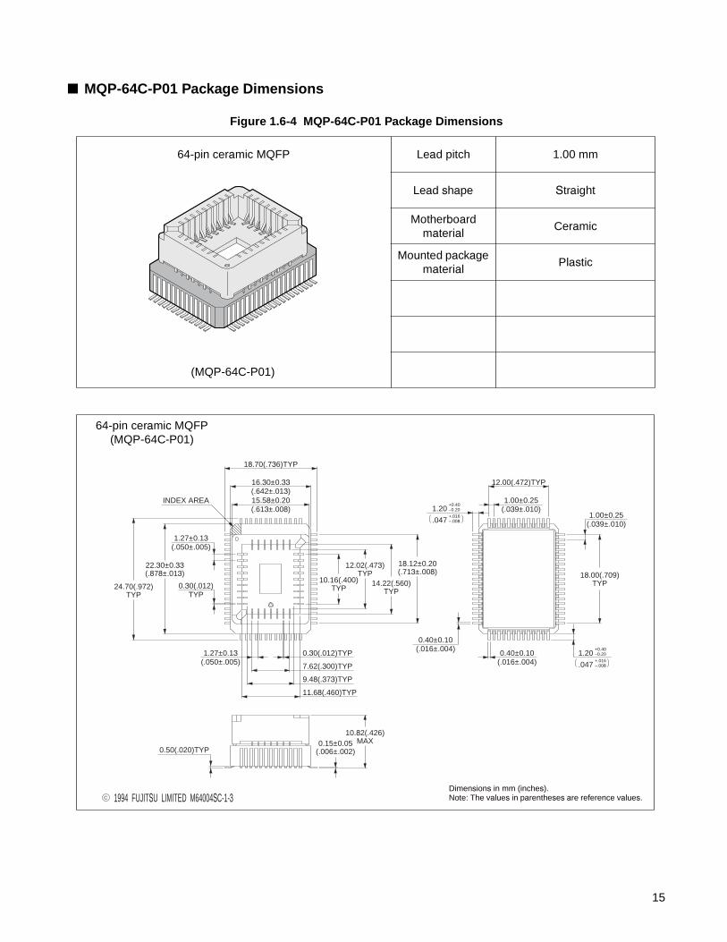
MQP-64C-P01 Package Dimensions
Figure 1.6-4 MQP-64C-P01 Package Dimensions
64-pin ceramic MQFP Lead pitch 1.00 mm
Lead shape Straight
Motherboard material
Ceramic
Mounted package material
Plastic
64-pin ceramic MQFP(MQP-64C-P01)
(MQP-64C-P01)
C 1994 FUJITSU LIMITED M64004SC-1-3
15.58±0.20(.613±.008)
16.30±0.33(.642±.013)
18.70(.736)TYP
INDEX AREA
0.30(.012)TYP
1.27±0.13(.050±.005)
22.30±0.33(.878±.013)
24.70(.972)TYP
10.16(.400)TYP
12.02(.473)TYP
14.22(.560)TYP
18.12±0.20(.713±.008)
1.27±0.13(.050±.005)
0.30(.012)TYP
7.62(.300)TYP
9.48(.373)TYP
11.68(.460)TYP
0.50(.020)TYP0.15±0.05
(.006±.002)
10.82(.426)MAX
0.40±0.10(.016±.004) .047 –.008
+.016
–0.20+0.40
1.20
0.40±0.10(.016±.004)
1.00±0.25(.039±.010)
18.00(.709)TYP
1.00±0.25(.039±.010)
12.00(.472)TYP
.047 –.008+.016
–0.20+0.40
1.20
Dimensions in mm (inches).Note: The values in parentheses are reference values.
15

CHAPTER 1 OVERVIEW
1.7 Pin Functions
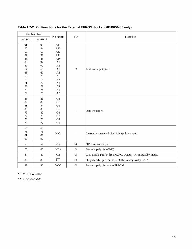
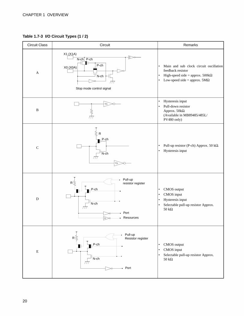
Table 1.7-1 and Table 1.7-2 list the MB89480/480L series I/O pins and their functions. Table 1.7-3 lists the I/O circuit types.The letter in the I/O Circuit Type column of Table 1.7-1 refers to the letter in the Circuit Class column of Table 1.7-3.
Pin Functions
Table 1.7-1 Pin Functions (1 / 3)
Pin Number
Pin NameI/O
Circuit Type
FunctionSH-DIP*1
MDIP*4
MQFP*2
QFP*3
33 26 25 X0A
Connection pins for a crystal or other oscillator. An external clock can be connected to X0. In this case, leave X1 open.34 27 26 X1
29 22 21 X0AA
Connection pins for a crystal or other oscillator of sub clock. An external clock can be connected to X0A (for low-speed: 32.768kHz). In this case, leave X1A open.30 23 22 X1A
35 28 27 MODE BInput pins for setting the memory access mode. Connect directly to VSS.
36 29 28 RST CReset I/O pin. The pin is a N-ch open-drain type with pull-up resistor and a hysteresis input. The pin outputs a "L" level when an internal reset request is present. Inputting an "L" level initializes internal circuits.
50 to 48 43 to 41 42 to 40P00/INT20
toP02/INT22
DGeneral-purpose CMOS I/O port. A hysteresis input.The pin is shared with external interrupt 2 input.
47 40 39 P03/INT23 D
General-purpose CMOS I/O port. A hysteresis input.The pin is shared with external interrupt 2 input, and shared with 8/16-bit timer/counter 21, 22 input when booster is selected.
46 39 38 P04/INT24 D
General-purpose CMOS I/O port. A hysteresis input.The pin is shared with external interrupt 2 input, andshared with 8/16-bit timer/counter 21, 22 output when booster is selected.
45 38 37P05/INT25/
PWCD
General-purpose CMOS I/O port. A hysteresis input.The pin is shared with external interrupt 2 input, and PWC input.
44 37 36P06/INT26/
PPGD
General-purpose CMOS I/O port. A hysteresis input.The pin is shared with external interrupt 2 input, and 6-bit PPG output.
43 36 35P07/INT27/
BUZD
General-purpose CMOS I/O port. A hysteresis input.The pin is shared with external interrupt 2 input and buzzer output.
16

25 to 28 18 to 21 17 to 20
P10/SEG23/INT10
toP13/SEG26/
INT13
F / KGeneral-purpose N-ch open-drain output port. A hysteresis input.The pin is shared with external interrupt 1 input and LCD segment output.
37 to 40 30 to 33 29 to 32
P14/SEG27/AN0
toP17/SEG30/
AN3
G / K
General-purpose N-ch open-drain output port. An analog input.The pin is shared with A/D converter input and LCD segment output. LCD segment output will be disabled when booster is selected.
51 44 43 P20/PWM EGeneral-purpose CMOS I/O port.The pin is shared with PWM output.
52 45 44 P21/SCK EGeneral-purpose CMOS I/O port. The pin is shared with UART/SIO clock I/O.
53 46 45 P22/SO EGeneral-purpose CMOS I/O port. The pin is shared with UART/SIO data output.
54 47 46 P23/SI DGeneral-purpose CMOS I/O port. The pin is shared with UART/SIO data input.
55 48 47 P24/C1/TO2 H
General-purpose CMOS I/O port.The pin is shared with 8/16-bit timer/counter 21,22 output (It is redirected to P04/INT24 when booster is selected), and operates as a capacitor connecting pin when booster is selected.
56 49 48 P25/C0/EC2 F
General-purpose CMOS I/O port.A hysteresis input.The pin is shared with 8/16-bit timer/counter 21,22 input (It is redirected to P03/INT23 when booster is selected), and operates as a capacitor connecting pin when booster is selected.
58 51 50 P26/V1/TO1 HGeneral-purpose CMOS I/O port.The pin is shared with 8/16-bit timer 11,12 output, and LCD power driving pin.
59 52 51 P27/V2/EC1 FGeneral-purpose CMOS I/O port.A hysteresis input.The pin is shared with 8/16-bit timer 11,12 input, and LCD power driving pin.
62 55 54 P30/COM2 I / KGeneral-purpose N-ch open-drain output port.The pin is shared with the LCD common output
61 54 53 P31/COM3 I / KGeneral-purpose N-ch open-drain output port.The pin is shared with the LCD common output
9 to 16 2 to 9 1 to 8P40/SEG8 to P47/SEG15
H / KGeneral-purpose N-ch open-drain I/O port.The pin is shared with LCD segment output.
17 to 23 10 to 16 9 to 15P50/SEG16
to P56/SEG22
H / KGeneral-purpose N-ch open-drain I/O port.The pin is shared with LCD segment output.
24 17 16 P57 J General-purpose CMOS input port
2 to 859 to 64,
158 to 64
SEG1 to SEG7
K LCD segment output only pins
1, 63 58, 56 57, 55COM0, COM1
K LCD common output only pins
Table 1.7-1 Pin Functions (2 / 3)
Pin Number
Pin NameI/O
Circuit Type
FunctionSH-DIP*1
MDIP*4
MQFP*2
QFP*3
17
CHAPTER 1 OVERVIEW
*1: DIP-64P-M01
*2: MQP-64C-P01
*3: FPT-64P-M09
*4: MDP-64C-P02
60 53 52 V3 — LCD driving power supply pin
57 50 49 V0/SEG0 — / KLCD driving power supply pin when booster is selected.LCD segment output only pin when booster is not selected.
31 24 23 C —
When MB89P485 is used, connect this pin to an external 0.1µF capacitor to ground.
When MB89485/L, MB89P485L or MB89PV480 is used, this pin will become a N.C. pin.
64 57 56 VCC — Power supply pin (+3V or +5V)
32 25 24 VSS — Power supply pin (GND)
41 34 33 AVCC — A/D converter power supply pin
42 35 34 AVSS —A/D converter power supply pin. Use at the same voltage level as VSS.
Table 1.7-1 Pin Functions (3 / 3)
Pin Number
Pin NameI/O
Circuit Type
FunctionSH-DIP*1
MDIP*4
MQFP*2
QFP*3
18
*1: MDP-64C-P02
*2: MQP-64C-P01
Table 1.7-2 Pin Functions for the External EPROM Socket (MB89PV480 only)
Pin NumberPin Name I/O Function
MDIP*1 MQFP*2
919066878588896768697071727374
959467918892936869707172737475
A14A13A12A11A10A9A8A7A6A5A4A3A2A1A0
O Address output pins
8382818079777675
8685848382797877
O8O7O6O5O4O3O2O1
I Data input pins
65768190
65768190
N.C. — Internally connected pins. Always leave open.
65 66 Vpp O "H" level output pin
78 80 VSS O Power supply pin (GND)
84 87 CE O Chip enable pin for the EPROM. Outputs "H" in standby mode.
86 89 OE O Output enable pin for the EPROM. Always outputs "L".
92 96 VCC O Power supply pin for the EPROM
19
CHAPTER 1 OVERVIEW
Table 1.7-3 I/O Circuit Types (1 / 2)
Circuit Class Circuit Remarks
A
• Main and sub clock circuit oscillationfeedback resistor
• High-speed side = approx. 500kΩ• Low-speed side = approx. 5MΩ
B
• Hysteresis input
• Pull-down resistor Approx. 50kΩ.(Available in MB89485/485L/PV480 only)
C• Pull-up resistor (P-ch) Approx. 50 kΩ.
• Hysteresis input
D
• CMOS output
• CMOS input
• Hysteresis input
• Selectable pull-up resistor Approx. 50 kΩ.
E
• CMOS output
• CMOS input
• Selectable pull-up resistor Approx. 50 kΩ.
X1 (X1A)
X0 (X0A)
N-ch P-ch
P-ch
N-ch
Stop mode control signal
P-ch
N-ch
R
P-ch
N-ch
R
Port
Resources
Pull-upresistor register
P-ch
N-ch
R
Port
Pull-upResistor register
20

F• N-ch open-drain output
• CMOS input
• Hysteresis input
G• N-ch open-drain output
• CMOS input
• Analog input
H• N-ch open-drain output
• CMOS input
I N-ch open-drain output
J CMOS input
K LCD segment output
Table 1.7-3 I/O Circuit Types (2 / 2)
Circuit Class Circuit Remarks
N-ch
Port
Resources
N-ch
Port
Analog input
N-ch
Port
N-ch
Port
N-ch
P-ch
P-ch
N-ch
21

CHAPTER 1 OVERVIEW
22
CHAPTER 2HANDLING DEVICES
This chapter describes points to note when using the general-purpose single-chip microcontroller.
2.1 Notes on Handling Devices
23
CHAPTER 2 HANDLING DEVICES
2.1 Notes on Handling Devices
This section lists points to note regarding the power supply voltage, pins, and other device handling aspects.
Notes on Handling Devices• Take great care not to exceed the maximum rated voltage (prevent latch-up).
Latch-up may occur on CMOS IC if voltage higher than VCC or lower than VSS is applied to input
and output pins other than medium- to high-withstand voltage pins, or if voltage higher than the
ratings is applied between VCC and VSS.
When latch-up occurs, power supply current increases rapidly and might thermally damage
elements. When using, take great care not to exceed the maximum ratings.
Also, take care to prevent the analog power supply (AVCC) and analog input from exceeding the
digital power supply (VCC) when the analog system power supply is turned on and off.
• Stabilizing supply voltage is important.
A rapid fluctuation of VCC power supply voltage could cause malfunctions, even if it occurs within
the operation assurance range of the voltage. The voltage must therefore be stabilized. As
stabilization guidelines, it is recommended to stabilize the voltage so that VCC ripple fluctuations
(peak to peak value) will be less than 10% of the standard VCC value at the commercial frequency
(50Hz to 60 Hz) and the transient fluctuation rate will be less than 0.1 V/ms at the time of a
momentary fluctuation such as when power is switched.
• Treatment of unused input pins
Leaving unused input pins open could cause malfunctions. They should be connected to a pull-up or
pull-down resistor.
• Treatment of N.C. pins
Be sure to leave (internally connected) N.C. pins open.
• Treatment of power supply pins on microcontroller with A/D converter
Connect to be AVCC = VCC and AVSS = VSS even if the A/D converter is not in use.
• Precautions when using an external clock
Even when an external clock is used, oscillation stabilization wait time is required for power-on reset
and wake-up from stop mode.
• MB89480/480L series C pin handling
Table 2.1-1 lists the connection of C pin:
Table 2.1-1 Connection of C pin
C pin connection
MB89485/485L/P485L/PV480 N.C. pin
MB89P485 This pin must be connected to an external 0.1µF capacitor to ground.
24

CHAPTER 3CPU
This chapter describes the functions and operation of the CPU in MB89480/480L series.
3.1 Memory Space
3.2 Dedicated Registers
3.3 General-purpose Registers
3.4 Interrupts
3.5 Resets
3.6 Clocks
3.7 Standby Modes (Low-Power Consumption)
3.8 Memory Access Mode
25
CHAPTER 3 CPU
3.1 Memory Space
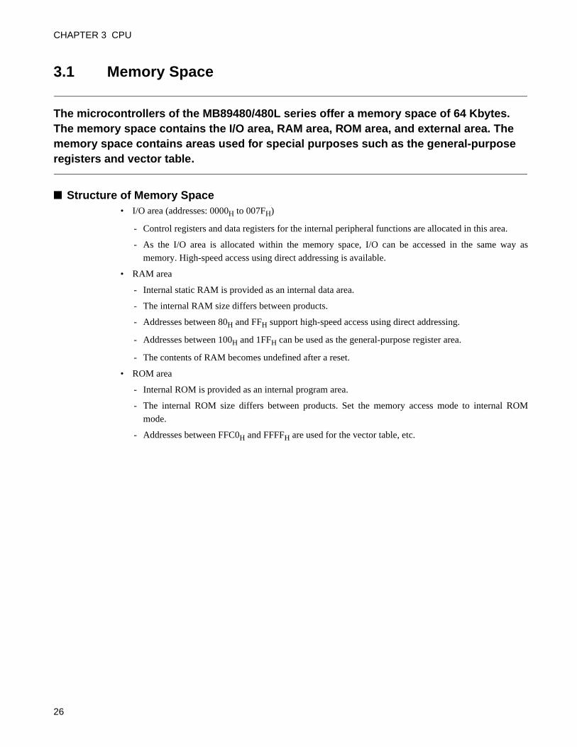
The microcontrollers of the MB89480/480L series offer a memory space of 64 Kbytes. The memory space contains the I/O area, RAM area, ROM area, and external area. The memory space contains areas used for special purposes such as the general-purpose registers and vector table.
Structure of Memory Space• I/O area (addresses: 0000H to 007FH)
- Control registers and data registers for the internal peripheral functions are allocated in this area.
- As the I/O area is allocated within the memory space, I/O can be accessed in the same way as
memory. High-speed access using direct addressing is available.
• RAM area
- Internal static RAM is provided as an internal data area.
- The internal RAM size differs between products.
- Addresses between 80H and FFH support high-speed access using direct addressing.
- Addresses between 100H and 1FFH can be used as the general-purpose register area.
- The contents of RAM becomes undefined after a reset.
• ROM area
- Internal ROM is provided as an internal program area.
- The internal ROM size differs between products. Set the memory access mode to internal ROM
mode.
- Addresses between FFC0H and FFFFH are used for the vector table, etc.
26

Memory Map
Figure 3.1-1 Memory Map
MB89P485/P485L
General-purposeregisters
I/O
RAM
ROM
0000H
0080H
0100H
0280H
FFFFH
0200H
Vacant
MB89485/485L
General-purposeregisters
I/O
RAM
ROM
0000H
0080H
0100H
0280H
FFFFH
0200H
Vacant
MB89PV480
General-purposeregisters
I/O
RAM
0000H
0080H
0100H
FFFFH
0200H
0480H
ROMExternal
(32K)
8000H
Vacant
C000HC000H
FFC0H FFC0H FFC0H
Vector table (reset, interrupt, vector call instruction)
27

CHAPTER 3 CPU
3.1.1 Special Purpose Areas
In addition to the I/O area, the special purpose areas in the memory space include the general-purpose register area and the vector table area.
General-purpose Register Area (Addresses: 0100H to 01FFH)
• Provides auxiliary registers for 8-bit arithmetic operation and transfer.
• Allocated to a part of the RAM area. Can also be used as normal RAM.
• Using the area as general-purpose registers enables high-speed access by general-purpose register
addressing using short instructions.
Reference:
See "3.2.2 Register Bank Pointer (RP)" and "3.3 General-purpose Registers" for details.
Vector Table Area (Addresses: FFC0H to FFFFH)
• Used as the vector table for the vector call instruction, interrupts, and resets.
• The vector table is allocated at the top of the ROM area. The start address of the correspondingprocessing routine is set as data at each vector table address.
Table 3.1-1 lists the vector table addresses referenced by the vector call instruction, interrupts, and resets.
Reference:
See "3.4 Interrupts", "3.5 Resets", and "(6) CALLV #vct" in "B.2 Special Instructions" for details.
28

Table 3.1-1 Vector Table
Vector call instruction
Vector table addressVector call instruction
Vector table address
Upper Lower Upper Lower
CALLV #0 FFC0H FFC1H IRQF FFDCH FFDDH
CALLV #1 FFC2H FFC3H IRQE FFDEH FFDFH
CALLV #2 FFC4H FFC5H IRQD FFE0H FFE1H
CALLV #3 FFC6H FFC7H IRQC FFE2H FFE3H
CALLV #4 FFC8H FFC9H IRQB FFE4H FFE5H
CALLV #5 FFCAH FFCBH IRQA FFE6H FFE7H
CALLV #6 FFCCH FFCDH IRQ9 FFE8H FFE9H
CALLV #7 FFCEH FFCFH IRQ8 FFEAH FFEBH
IRQ7 FFECH FFEDH
IRQ6 FFEEH FFEFH
IRQ5 FFF0H FFF1H
IRQ4 FFF2H FFF3H
IRQ3 FFF4H FFF5H
IRQ2 FFF6H FFF7H
IRQ1 FFF8H FFF9H
IRQ0 FFFAH FFFBH
Mode data — FFFDH
Reset vector FFFEH FFFFH
29

CHAPTER 3 CPU
3.1.2 Storing 16-bit Data in Memory
For 16-bit data and the stack, store the upper data in the lower memory address value.
Storing 16-bit Data in RAMWhen writing 16-bit data to memory, store the upper byte at the lower address and the lower byte at the
next address. Handle reading of 16-bit data in the same way. Figure 3.1-2 shows how 16-bit data is stored
in memory
Figure 3.1-2 Storing 16-bit Data in Memory
Storing 16-bit OperandsThe byte order applies when specifying a 16-bit operand in an instruction. Store the upper byte at the
address following the operation code (instruction) and the lower byte at the next address.
The byte ordering applies to both 16-bit immediate data and operands that specify a memory address.
Figure 3.1-3 shows how 16-bit data is stored in an instruction.
Figure 3.1-3 Storing of 16-bit Data in an Instruction
Storing 16-bit Data on StackThe same byte order applies when saving data of 16-bit register on the stack during an interrupt or similar.
The upper byte is stored in the lower address.
Before execution
1 2 3 4 H
0080H
0081H
0082H
0083H
A
0080H
0081H
0082H
0083H
After execution
1 2 3 4 H12H
34H
Memory Memory
MOVW 0081H,A
A
.
.
.
[Example] MOV A,5678H ; Extended addressMOVW A,#1234H ; 16-bit immediate data
X X X 0 H XX XXX X X 2 H 60 56 78 ; Extended addressX X X 5 H E4 12 34 ; 16-bit immediate dataX X X 8 H XX
.
.
.
After assembly
30
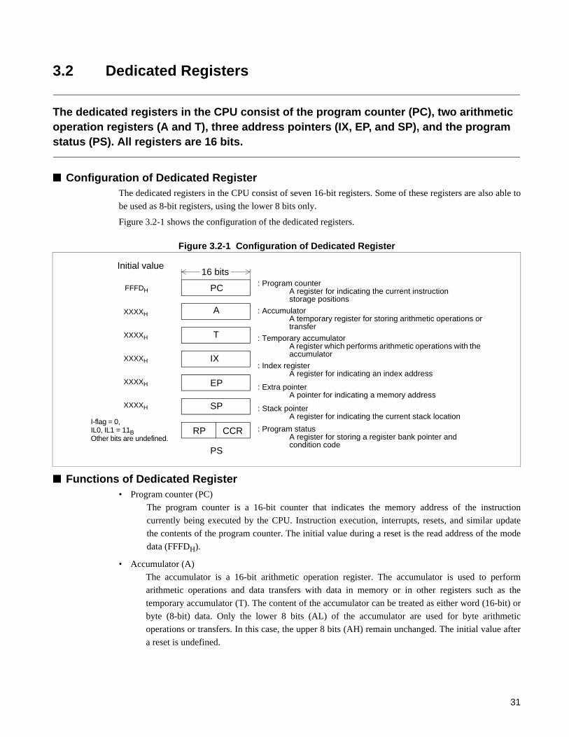
3.2 Dedicated Registers
The dedicated registers in the CPU consist of the program counter (PC), two arithmetic operation registers (A and T), three address pointers (IX, EP, and SP), and the program status (PS). All registers are 16 bits.
Configuration of Dedicated RegisterThe dedicated registers in the CPU consist of seven 16-bit registers. Some of these registers are also able to
be used as 8-bit registers, using the lower 8 bits only.
Figure 3.2-1 shows the configuration of the dedicated registers.
Figure 3.2-1 Configuration of Dedicated Register
Functions of Dedicated Register• Program counter (PC)
The program counter is a 16-bit counter that indicates the memory address of the instruction
currently being executed by the CPU. Instruction execution, interrupts, resets, and similar update
the contents of the program counter. The initial value during a reset is the read address of the mode
data (FFFDH).
• Accumulator (A)
The accumulator is a 16-bit arithmetic operation register. The accumulator is used to perform
arithmetic operations and data transfers with data in memory or in other registers such as the
temporary accumulator (T). The content of the accumulator can be treated as either word (16-bit) or
byte (8-bit) data. Only the lower 8 bits (AL) of the accumulator are used for byte arithmetic
operations or transfers. In this case, the upper 8 bits (AH) remain unchanged. The initial value after
a reset is undefined.
PC
A
T
IX
EP
SP
RP CCR
16 bits
PS
Initial value
XXXXH
XXXXH
XXXXH
XXXXH
XXXXH
FFFDH: Program counter
A register for indicating the current instruction storage positions
: AccumulatorA temporary register for storing arithmetic operations ortransfer
: Temporary accumulatorA register which performs arithmetic operations with the accumulator
: Index registerA register for indicating an index address
: Extra pointerA pointer for indicating a memory address
: Stack pointerA register for indicating the current stack location
: Program statusA register for storing a register bank pointer and condition code
I-flag = 0,IL0, IL1 = 11BOther bits are undefined.
31

CHAPTER 3 CPU
• Temporary accumulator (T)
The temporary accumulator is an auxiliary 16-bit arithmetic operation register used to perform
arithmetic operations with the data in the accumulator (A). The content of the temporary
accumulator is treated as word data (16-bit) for word-length arithmetic operations with the
accumulator and as byte data (8-bit) for byte-length arithmetic operations. For byte-length
arithmetic operations, only the lower 8 bits of the temporary accumulator (TL) are used and the
upper 8 bits (TH) are not used.
Transferring data to the accumulator (A) automatically transfers the previous content of the
accumulator to the temporary accumulator. In this case also, a byte transfer leaves the upper 8 bits
of the temporary accumulator (TH) unchanged. The initial value after a reset is undefined.
• Index register (IX)
The index register is a 16-bit register used to hold the index address. The index register is used in
conjunction with a single byte offset value (-128 to +127). Adding the sign-extended offset value to
the index address generates the memory address for data access. The initial value after a reset is
undefined.
• Extra pointer (EP)
The extra pointer is a 16-bit register used to hold a memory address for data access. The initial value
after a reset is undefined.
• Stack pointer (SP)
The stack pointer is a 16-bit register used to hold the address referenced during operations such as
interrupts, subroutine calls, and the stack save and restore instructions. The value of the stack
pointer during program execution is the address of the most recently saved data on the stack. The
initial value after a reset is undefined.
• Program status (PS)
The program status is a 16-bit control register. The upper 8 bits contain the register bank pointer
(RP) which points to the address of the current general-purpose register bank.
The lower 8 bits contain the condition code register (CCR) which contains flags indicating the
current CPU status. The two 8-bit registers which form the program status cannot be accessed
independently (the program status can only be accessed by the MOVW A,PS and MOVW PS,A
instructions).
Refer to the F2MC-8L MB89600 series Programming Manual for details on using the dedicatedregisters.
32

3.2.1 Condition Code Register (CCR)
The condition code register (CCR) located in the lower 8 bits of the program status (PS) consists of the C, V, Z, N, and H bits indicating the results of arithmetic operations and the contents of transfer data, and the I, IL1, and IL0 bits for control whether or not the CPU accepts interrupt requests.
Structure of Condition Code Register (CCR)
Figure 3.2-2 Structure of Condition Code Register (CCR)
• Half-carry flag (H)
This flag is set to "1" when a carry from bit3 to bit4 or a borrow from bit4 to bit3 occurs as a result
of an arithmetic operation. It is cleared to "0" otherwise. As this flag is for the decimal adjustment
instructions, do not use this flag in cases other than addition or subtraction.
• Negative flag (N)
This flag is set to "1" if the most significant bit (MSB) is set to "1" as a result of an arithmetic
operation. It is cleared to "0" when the bit is set to "0".
• Zero flag (Z)
This flag is set to "1" when an arithmetic operation results is "0". It is cleared to "0" otherwise.
• Overflow flag (V)
This flag is set to "1" if the complement on 2 overflows as a result of an arithmetic operation. It is
cleared to "0" if the overflow does not occur.
• Carry flag (C)
This flag is set to "1" when a carry from bit7 or borrow to bit7 occurs as a result of an arithmetic
operation. It is cleared to "0" otherwise. Set to the shift-out value in case of a shift instruction.
Figure 3.2-3 shows the change of the carry flag by a shift instruction.
Half-carry flagInterrupt enable flagInterrupt level bitsNegative flagZero flagOverflow flagCarry flag
bit15 14 13 12 11 10 9 8 7 6 5 4 3 2 1 0
R4 R3 R2 R1 R0 — — — H I IL1 IL0 N Z V C
CCR initial value
X011XXXXB
RP CCR
PS
X: Undefined value
33
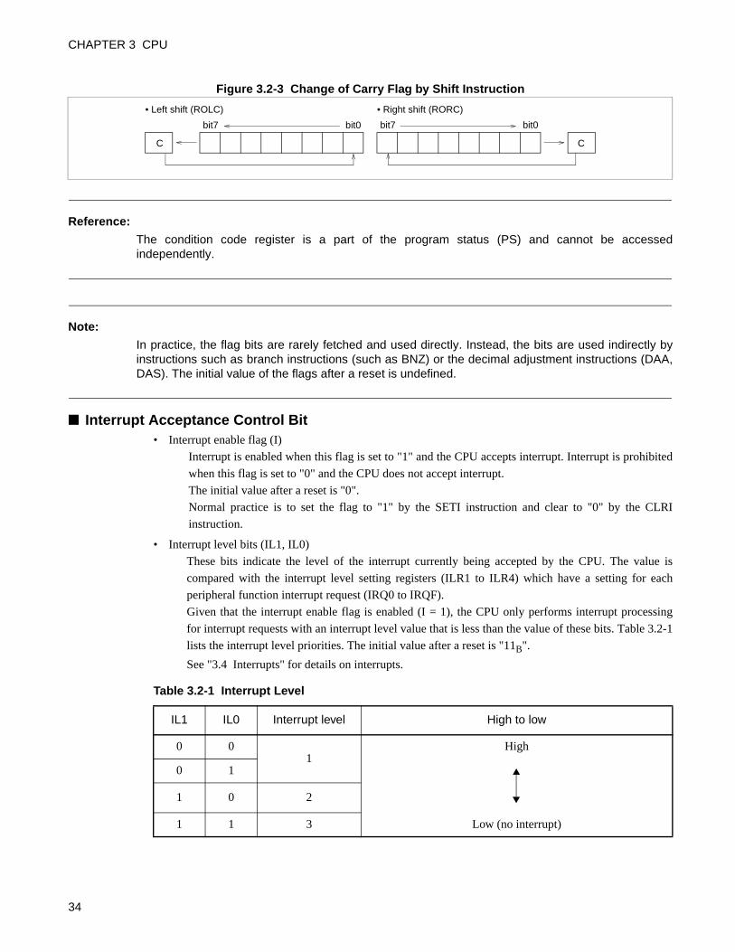
CHAPTER 3 CPU
Figure 3.2-3 Change of Carry Flag by Shift Instruction
Reference:
The condition code register is a part of the program status (PS) and cannot be accessedindependently.
Note:
In practice, the flag bits are rarely fetched and used directly. Instead, the bits are used indirectly byinstructions such as branch instructions (such as BNZ) or the decimal adjustment instructions (DAA,DAS). The initial value of the flags after a reset is undefined.
Interrupt Acceptance Control Bit• Interrupt enable flag (I)
Interrupt is enabled when this flag is set to "1" and the CPU accepts interrupt. Interrupt is prohibited
when this flag is set to "0" and the CPU does not accept interrupt.
The initial value after a reset is "0".
Normal practice is to set the flag to "1" by the SETI instruction and clear to "0" by the CLRI
instruction.
• Interrupt level bits (IL1, IL0)
These bits indicate the level of the interrupt currently being accepted by the CPU. The value is
compared with the interrupt level setting registers (ILR1 to ILR4) which have a setting for each
peripheral function interrupt request (IRQ0 to IRQF).
Given that the interrupt enable flag is enabled (I = 1), the CPU only performs interrupt processing
for interrupt requests with an interrupt level value that is less than the value of these bits. Table 3.2-1
lists the interrupt level priorities. The initial value after a reset is "11B".
See "3.4 Interrupts" for details on interrupts.
C
bit7 bit0 bit7 bit0
• Left shift (ROLC) • Right shift (RORC)
C
Table 3.2-1 Interrupt Level
IL1 IL0 Interrupt level High to low
0 01
High
0 1
1 0 2
1 1 3 Low (no interrupt)
34

Note:
The interrupt level bits (IL1, IL0) are normally "11B" when the CPU is not processing an interrupt(during main program execution).
35

CHAPTER 3 CPU
3.2.2 Register Bank Pointer (RP)
The register bank pointer (RP) located in the upper 8 bits of the program status (PS) indicates the address of the general-purpose register bank currently in use. The RP is converted to form the actual address in general-purpose register addressing.
Configuration of Register Bank Pointer (RP) Figure 3.2-4 shows the configuration of the register bank pointer (RP).
Figure 3.2-4 Configuration of Register Bank Pointer (RP)
The register bank pointer indicates the address of the register bank currently in use. Figure 3.2-5 shows the
relationship between the pointer contents and the actual address is based on the conversion rule.
Figure 3.2-5 Rule for Conversion of Actual Addresses of General-purpose Register Area
• The register bank pointer points to the memory block (register bank) in the RAM area that is used forgeneral-purpose registers. A total of 32 register banks are available. A register bank is specified bysetting a value between 0 and 31 in the upper 5 bits of the register bank pointer. Each register bankcontains 8-bit general-purpose registers. Registers are specified by the lower 3 bits of the operationcodes.
• Using the register bank pointer, the addresses 0100H to 01FFH can be used as the general-purposeregister area. However, the available area is limited on some products if internal RAM only is used. Theinitial value after a reset is undefined.
Notes:
• The register bank pointer is a part of the program status (PS) and cannot be accessed independently.
• The register bank pointer must be set before using the general purpose register.
bit15 14 13 12 11 10 9 8 7 6 5 4 3 2 1 0
R4 R3 R2 R1 R0 — — — H I IL1 IL0 N Z V C
RP initial value
XXXXXXXXB
RP CCR
PS
X: Undefined value
A15 A14 A13 A12 A10 A11 A9 A8 A7 A6 A5 A4 A3 A2 A1 A0
"0" "0" "0" "0" "0" "0" "0" "1" R4 R3 R2 R1 R0 b2 b1 b0
Upper bits of RP Lower operation codes
Generated addresses
36
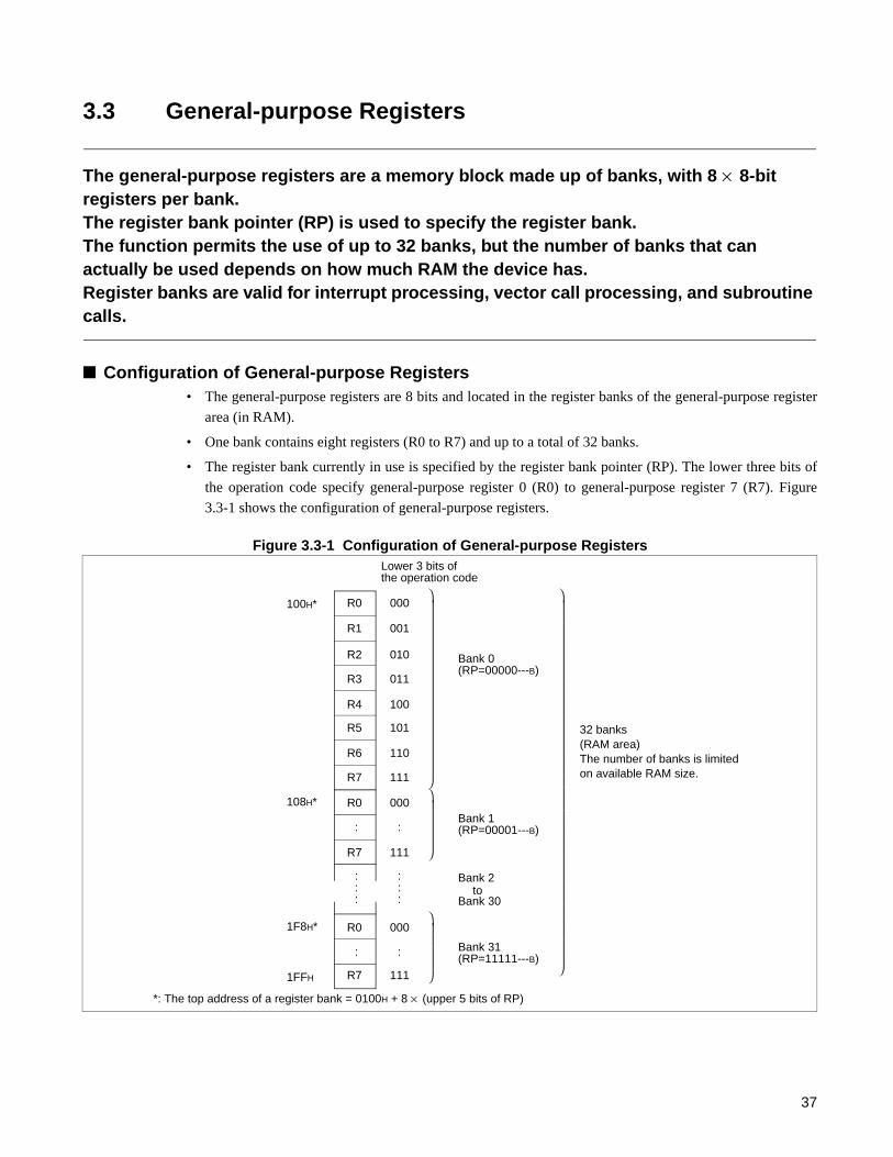
3.3 General-purpose Registers
The general-purpose registers are a memory block made up of banks, with 8 × 8-bit registers per bank.The register bank pointer (RP) is used to specify the register bank.The function permits the use of up to 32 banks, but the number of banks that can actually be used depends on how much RAM the device has.Register banks are valid for interrupt processing, vector call processing, and subroutine calls.
Configuration of General-purpose Registers• The general-purpose registers are 8 bits and located in the register banks of the general-purpose register
area (in RAM).
• One bank contains eight registers (R0 to R7) and up to a total of 32 banks.
• The register bank currently in use is specified by the register bank pointer (RP). The lower three bits of
the operation code specify general-purpose register 0 (R0) to general-purpose register 7 (R7). Figure
3.3-1 shows the configuration of general-purpose registers.
Figure 3.3-1 Configuration of General-purpose RegistersLower 3 bits of the operation code
*: The top address of a register bank = 0100H + 8 × (upper 5 bits of RP)
R0
R1
R2
R3
R4
R5
R6
R7
R0
R7
R0
R7
:
:::
:
000
001
010
011
100
101
110
111
000
111
000
111
100H*
108H*
1FFH
1F8H*
:
:::
:
Bank 0(RP=00000---B)
Bank 1(RP=00001---B)
Bank 31(RP=11111---B)
Bank 2to
Bank 30
⎞⎟⎟⎟⎟⎟⎟⎟⎟⎟⎟⎟⎟⎟⎟⎟⎠⎞⎟⎟⎟⎟⎠
⎞⎟⎟⎟⎟⎠
⎞⎟⎟⎟⎟⎟⎟⎟⎟⎟⎟⎟⎟⎟⎟⎟⎟⎟⎟⎟⎟⎟⎟⎟⎟⎟⎟⎟⎟⎟⎟⎟⎠
32 banks(RAM area)The number of banks is limitedon available RAM size.
37

CHAPTER 3 CPU
Reference:
See "3.1.1 Special Purpose Areas" for the general-purpose register area available for each product.
Features of General-purpose RegistersGeneral-purpose registers have the following features:
• RAM can be accessed at high-speed using short instructions (general-purpose register addressing).
• Registers are grouped in blocks in the form of register banks. This simplifies the process of saving
register contents and dividing registers by function.
Dedicated register banks can be fixedly assigned for each interrupt processing or vector call (CALLV #0 to
#7) processing routine by general-purpose register. For example, register bank 4 is used for interrupt 2.
For example, a particular interrupt processing routine only uses a particular register bank which cannot be
written to unintentionally by other routines. The interrupt processing routine only needs to specify its
dedicated register bank at the start of the routine to effectively save the general-purpose registers in use
prior to the interrupt. Therefore, saving the general-purpose registers to the stack or other memory location
is not necessary. This allows high-speed interrupt handling while maintaining simplicity.
Also, as an alternative to saving general-purpose registers in subroutine calls, register banks can be used to
create reentrant programs (programs that do not use fixed addresses and can be entered more than once)
usually made by the index register (IX).
Note:
If an interrupt processing routine changes the register bank pointer (RP), ensure that the programdoes not also change the interrupt level bits in the condition code register (CCR: IL1, IL0) whenspecifying the register bank.
38

3.4 Interrupts
The MB89480/480L series has 15 interrupt request input corresponding to peripheral functions. An interrupt level can be set independently.If an interrupt request output is enabled in the peripheral function, an interrupt request from a peripheral function is compared with the interrupt level in the interrupt controller. The CPU performs interrupt operation according to how the interrupt is accepted. The interrupt request wakes up from standby modes, and returns to the interrupt or normal operation.
Interrupt Requests from Peripheral FunctionsTable 3.4-1 lists the interrupt requests corresponding to the peripheral functions. On acceptance of an
interrupt, execution branches to the interrupt processing routine. The contents of interrupt vector table
address corresponding to the interrupt request specifies the branch destination address for the interrupt
processing routine.
An interrupt processing level can be set for each interrupt request in the interrupt level setting registers
(ILR1, ILR2, ILR3, ILR4). Three levels are available.
If an interrupt request with the same or lower level occurs during execution of an interrupt processing
routine, the latter interrupt is not normally processed until the current interrupt processing routine
completes. If interrupt request set the same level occur simultaneously, the highest priority is IRQ0.
Table 3.4-1 Interrupt Request and Interrupt Vector
Interrupt requestVector table address Bit names of the
interrupt level setting register
Simultaneously-generated same-level IRQ priorityUpper Lower
IRQ0 (External interrupt 1-1) FFFAH FFFBH L01, L00
IRQ1 (External interrupt 1-2) FFF8H FFF9H L11, L10
IRQ2 (External interrupt 1-3) FFF6H FFF7H L21, L20
IRQ3 (External interrupt 1-4) FFF4H FFF5H L31, L30
IRQ4 (External interrupt 2) FFF2H FFF3H L41, L40
IRQ5 (UART/SIO) FFF0H FFF1H L51, L50
IRQ6 (8/16-bit Timer ch.1) FFEEH FFEFH L61, L60
IRQ7 (8/16-bit Timer ch.2) FFECH FFEDH L71, L70
IRQ8 (A/D Converter) FFEAH FFEBH L81, L80
IRQ9 (PWM) FFE8H FFE9H L91, L90
IRQA (PWC) FFE6H FFE7H LA1, LA0
IRQB (Time-base timer) FFE4H FFE5H LB1, LB0
IRQC (Watch prescaler) FFE2H FFE3H LC1, LC0
IRQD (Vacancy) FFE0H FFE1H LD1, LD0
IRQE (Vacancy) FFDEH FFDFH LE1, LE0
IRQF (reserved for FLASH testing) FFDCH FFDDH LF1, LF0
High
Low
39
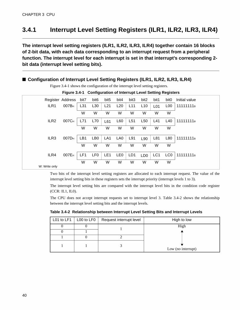
CHAPTER 3 CPU
3.4.1 Interrupt Level Setting Registers (ILR1, ILR2, ILR3, ILR4)
The interrupt level setting registers (ILR1, ILR2, ILR3, ILR4) together contain 16 blocks of 2-bit data, with each data corresponding to an interrupt request from a peripheral function. The interrupt level for each interrupt is set in that interrupt’s corresponding 2-bit data (interrupt level setting bits).
Configuration of Interrupt Level Setting Registers (ILR1, ILR2, ILR3, ILR4)Figure 3.4-1 shows the configuration of the interrupt level setting registers.
Figure 3.4-1 Configuration of Interrupt Level Setting Registers
Two bits of the interrupt level setting registers are allocated to each interrupt request. The value of the
interrupt level setting bits in these registers sets the interrupt priority (interrupt levels 1 to 3).
The interrupt level setting bits are compared with the interrupt level bits in the condition code register
(CCR: IL1, IL0).
The CPU does not accept interrupt requests set to interrupt level 3. Table 3.4-2 shows the relationship
between the interrupt level setting bits and the interrupt levels.
Register Address bit7 bit6 bit5 bit4 bit3 bit2 bit1 bit0 Initial value
ILR1 007BH L31 L30 L21 L20 L11 L10 L01 L00 11111111B
W W W W W W W W
ILR2 007CH L71 L70 L61 L60 L51 L50 L41 L40 11111111B
W W W W W W W W
ILR3 007DH LB1 LB0 LA1 LA0 L91 L90 L81 L80 11111111B
W W W W W W W W
ILR4 007EH LF1 LF0 LE1 LE0 LD1 LD0 LC1 LC0 11111111B
W W W W W W W WW: Write only
Table 3.4-2 Relationship between Interrupt Level Setting Bits and Interrupt Levels
L01 to LF1 L00 to LF0 Request interrupt level High to low
0 01
High
Low (no interrupt)
0 1
1 0 2
1 1 3
40

Notes:
• The interrupt level bits in the condition code register (CCR: IL1, IL0) are normally "11B" duringmain program execution.
• As the IRL1, ILR2, ILR3 and ILR4 registers are write only, the bit manipulation instructions cannotbe used.
41

CHAPTER 3 CPU
3.4.2 Interrupt Processing
The interrupt controller transmits the interrupt level to the CPU when an interrupt request is generated by a peripheral function. If the CPU is able to receive the interrupt, the CPU temporarily halts the currently executing program and executes the interrupt processing routine.
Interrupt ProcessingThe procedure for interrupt operation is performed in the following order: interrupt source generated at
peripheral function, set the interrupt request flag bit (request FF), discriminate the interrupt request enable
bit (enable FF), the interrupt level (ILR1, ILR2, ILR3, ILR4 and CCR: IL1, IL0), simultaneously generated
interrupt requests with the same level, then check the interrupt enable flag (CCR: I). Figure 3.4-2 shows the
interrupt processing.
42

Figure 3.4-2 Interrupt Processing
START
Initialize peripheral
Is an interrupt request present at the
peripheral?
Is interrupt request output enabled
for the peripheral?
Check the interrupt priority level
and transfer the level to the CPU
Compare the level with the IL bits in PS
Is the level higher than IL?
I-flag = 1?
Interrupt processing routine
Clear interrupt request
Execute interrupt processing
RETI
Restore PC and PS
Save PC and PS to the stack
PC ← interrupt vector
Update IL in PS
Inte
rnal
bus
Register file
IPLA
IR
PS I IL
Condition code register (CCR)
Check Comparator
Wake-up fromF2MC-8L·CPU
RAM
(5)
(7)
(6)
(3)
(4)
Enable FF
Request FFAND
Peripherals Leve
l com
para
tor
Interrupt controller
(1)
(3)
(4)
(5)
(7) (6)
···
YES
YES
YES
YES
NO
NO
NO
NO
stop modeWake-up from sleep mode
Main programexecution
(2)
43
CHAPTER 3 CPU
(1) After a reset, all interrupt requests are disabled.Initialize the peripheral functions that are to generate interrupts in the peripheral function initialization program, set the interrupt levels in the appropriate interrupt level setting registers (ILR1, ILR2, ILR3, ILR4), and start peripheral function.The interrupt level can be set to 1, 2 or 3. Level 1 is the highest priority, followed by level 2. Setting level 3 disables the interrupt for that peripheral function.
(2) Execute the main program (for multiple interrupts, execute the interrupt processing routine).
(3) The interrupt request flag bit (request FF) for a peripheral function is set to "0" when theperipheral function generates an interrupt source. If the interrupt request enable bit for theperipheral function is set to "enable" (enable FF = 1), the peripheral function outputs theinterrupt request to the interrupt controller.
(4) The interrupt controller continuously monitors for interrupt requests from the peripheralfunctions and passes the interrupt level of the current interrupt request with the highest interruptlevel to the CPU. The interrupt controller also evaluates the priority order if requests with thesame level are present simultaneously.
(5) If the interrupt level received by the CPU has a higher priority (a lower level value) than thelevel set in the interrupt level bits in the condition code register (CCR: IL1, IL0), the CPUchecks the interrupt enable flag (CCR: I) and receives the interrupt if interrupts are enabled(CCR: I = 1).
(6) The CPU saves the contents of the program counter (PC) and program status (PS) on the stack,reads the top address of the interrupt processing routine from the interrupt vector table for theinterrupt, updates the interrupt level bits in the condition code register (CCR: IL1, IL0) with thereceived interrupt level, and starts execution of the interrupt processing routine.
(7) Finally, on execution of the RETI instruction, the CPU restores the program counter (PC) andprogram status (PS) values saved on the stack and resumes execution from the instructionfollowing the last instruction executed before the interrupt.
Notes:
• As the interrupt request flag bit of a peripheral function is not cleared automatically when aninterrupt request is received, the bit must be cleared by the program (normally, by writing "0" tothe interrupt request flag bit) at interrupt processing routine.
• If the interrupt request flag bit is cleared at the top of the interrupt processing routine, theperipheral function that has generated the interrupt becomes able to generate another interruptduring execution of the interrupt processing routine (resetting the interrupt request flag bit).However, the interrupts are not normally accepted until the current processing routine completes.
Reference:
An interrupt wakes up the CPU from standby mode (low-power consumption). See "3.7 StandbyModes (Low-Power Consumption)" for details.
44

3.4.3 Multiple Interrupts
Multiple interrupts can be performed by setting different interrupt levels to the interrupt level setting registers for two or more interrupt requests from peripheral functions.
Multiple InterruptsIf the interrupt request having the higher interrupt levels occurs during the interrupt processing routines, the
CPU halts the current interrupt process and switches to accept the interrupt with the higher priority.
Interrupt levels can be set in the range 1 to 3. However, the CPU does not accept interrupt requests set to
interrupt level 3.
• Example of multiple interrupts
As an example of multiple interrupt processing, assume that an external interrupt has a higher
priority than the timer interrupt. The timer interrupt is set to level 2 and the external interrupt is set
to level 1. Figure 3.4-3 shows the processing when the external interrupt occurs during execution of
timer interrupt processing.
Figure 3.4-3 Example of Multiple Interrupts
• During execution of timer interrupt processing, the interrupt level bits in the condition code register
(CCR:IL1, IL0) are automatically set to the same value as the interrupt level setting registers (ILR1,
ILR2, ILR3, ILR4) corresponding to the timer interrupt (level 2 in this example). If the interrupt request
set to higher interrupt level (level 1 in this example) occurs at this time, the interrupt processing has
priority.
• To temporarily disable multiple interrupts during the timer interrupt, the interrupt enable flag in the
condition code register is set to "interrupts disabled" (CCR: I = 0) or the interrupt level bits (IL1, IL0)
set to "00B".
• On execution of the interrupt return instruction (RETI) at the completion of interrupt processing, the
CPU restores the program counter (PC) and program status (PS) values saved on the stack and resumes
execution of the interrupted program. Restoring the program status (PS) returns the condition code
register (CCR) to the value prior to the interrupt.
(4)
(5)(6)
(7)
(1)
(2) (3)
(8)
Main program
Initialize peripheral
Timer interrupt occurs
Restart main program
Interrupt level 2 (CCR:IL1, IL0 = 10B)
Timer interrupt processing
External interrupt
Halt
Restart
Timer interrupt
Timer interrupt returnsprocessing
Interrupt level 1 (CCR:IL1, IL0 = 01B)
External interrupt processing
External interrupt processing
External interrupt returns
occurs
45
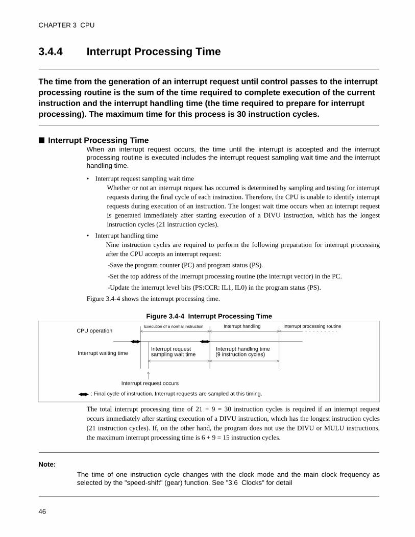
CHAPTER 3 CPU
3.4.4 Interrupt Processing Time
The time from the generation of an interrupt request until control passes to the interrupt processing routine is the sum of the time required to complete execution of the current instruction and the interrupt handling time (the time required to prepare for interrupt processing). The maximum time for this process is 30 instruction cycles.
Interrupt Processing TimeWhen an interrupt request occurs, the time until the interrupt is accepted and the interruptprocessing routine is executed includes the interrupt request sampling wait time and the interrupthandling time.
• Interrupt request sampling wait timeWhether or not an interrupt request has occurred is determined by sampling and testing for interruptrequests during the final cycle of each instruction. Therefore, the CPU is unable to identify interruptrequests during execution of an instruction. The longest wait time occurs when an interrupt requestis generated immediately after starting execution of a DIVU instruction, which has the longestinstruction cycles (21 instruction cycles).
• Interrupt handling timeNine instruction cycles are required to perform the following preparation for interrupt processingafter the CPU accepts an interrupt request:
-Save the program counter (PC) and program status (PS).
-Set the top address of the interrupt processing routine (the interrupt vector) in the PC.
-Update the interrupt level bits (PS:CCR: IL1, IL0) in the program status (PS).
Figure 3.4-4 shows the interrupt processing time.
Figure 3.4-4 Interrupt Processing Time
The total interrupt processing time of 21 + 9 = 30 instruction cycles is required if an interrupt request
occurs immediately after starting execution of a DIVU instruction, which has the longest instruction cycles
(21 instruction cycles). If, on the other hand, the program does not use the DIVU or MULU instructions,
the maximum interrupt processing time is 6 + 9 = 15 instruction cycles.
Note:
The time of one instruction cycle changes with the clock mode and the main clock frequency asselected by the "speed-shift" (gear) function. See "3.6 Clocks" for detail
CPU operation
Interrupt waiting time
Execution of a normal instruction
Interrupt request sampling wait time
Interrupt request occurs
Interrupt handling
Interrupt handling time (9 instruction cycles)
Interrupt processing routine
: Final cycle of instruction. Interrupt requests are sampled at this timing.
46

3.4.5 Stack Operation during Interrupt Processing
This section describes the saving of the register contents to the stack and restore operation during interrupt processing.
Stack Operation during Interrupt ProcessingThe CPU automatically saves the current contents of the program counter (PC) and program status (PS) to
the stack when an interrupt is accepted.
Figure 3.4-5 shows the stack operation at the start of interrupt processing.
Figure 3.4-5 Stack Operation during Interrupt Processing
Stack Operation at Interrupt ReturnOn execution of the interrupt return instruction (RETI) at the completion of interrupt processing, the CPU
performs the opposite processing to interrupt initiation, restoring first the program status (PS) and then the
program counter (PC) from the stack. This returns the PS and PC to their states immediately prior to the
start of the interrupt.
Note:
The CPU does not automatically save the contents of the accumulator (A) or temporary accumulator(T) contents to the stack. Use the PUSHW and POPW instructions to save and restore A and Tcontents to and from the stack.
× × H
× × H
× × H
× × H
× × H
× × H
027CH
027DH
027EH
027FH
0280H
0281H
Address Memory
0870HPS
E000HPC
0280HSP
Immediately before interrupt
08H
70H
E0H
00H
× × H
× × H
027CH
027DH
027EH
027FH
0280H
0281H
Address Memory
027CHSP
0870HPS
E000HPC
Immediately afterinterrupt
PS
PC
⎫⎬⎭⎫⎬⎭
47

CHAPTER 3 CPU
3.4.6 Stack Area for Interrupt Processing
Interrupt processing execution uses the stack area in RAM. The contents of the stack pointer (SP) specifies the top address of the stack area.
Stack Area for Interrupt ProcessingThe subroutine call instruction (CALL) and vector call instruction (CALLV) use the stack area to save and
restore the program counter (PC). The stack area is also used by the PUSHW and POPW instructions to
temporarily save and restore registers.
• The stack area is located in RAM along with the data area.
• Initializing the stack pointer (SP) to the top address of RAM and allocating data areas upwards from the
bottom RAM address is recommended.
Figure 3.4-6 shows the example of stack area setting.
Figure 3.4-6 Stack Area for Interrupt Processing
Note:
The stack area is used in the downward direction starting from a high address by functions such asinterrupts, subroutine calls, and the PUSHW instruction. Instructions such as return instructions(RETI, RET) and the POPW instruction release stack area in the upward direction. Take care whenthe stack address is decreased by multiple interrupts or subroutine calls that the stack does notoverlap the general-purpose register area or data areas containing other data.
General-purposeregisters
I/O
RAM
Access
ROM
0000H
0080H
0100H
0200H
FFFFH
0480H Recommended set value for SP
Data area
Stack area
(When the top address of RAM is 0480H.)
prohibited
48

3.5 Resets
The MB89480/480L series supports the following four types of reset source:• External reset• Software reset• Watchdog reset• Power-on reset
Reset Source
• External reset
Inputting an "L" level to the external reset pin (RST) generates an external reset. Returning the reset
pin to the "H" level disables the external reset.
When power is turned on or for external resets in stop mode, the reset operation is performed after
the oscillation stabilization wait time has passed and the external reset is released.
The external reset pin can also function as a reset output pin.
• Software reset
Writing "0" to the software reset bit in the standby control register (STBC: RST) generates a four-
instruction cycle reset. The software reset does not wait for the oscillation stabilization wait time.
• Watchdog reset
The watchdog reset generates a four-instruction cycle reset if data is not written to the watchdog
timer control register (WDTC) within a fixed time after the watchdog timer starts. The watchdog
reset does not wait for the oscillation stabilization wait time.
• Power-on reset
Turning on the power generates a reset. The reset operation is performed after the oscillation
stabilization wait time has passed.
Note:
Please select "There is power-on reset" and "Reset output and exist" by the mask option when youuse the device without inputting external reset when the power supply is turned on.
Table 3.5-1 Reset Source
Reset source Reset conditions
External reset Set the external reset pin to the "L" level.
Software reset Write "0" to the software reset bit in the standby control register (STBC: RST).
Watchdog reset Watchdog timer overflow
Power-on reset Power is turned on.
49

CHAPTER 3 CPU
Main Clock Oscillation Stabilization Wait Time and the Reset Source
Whether there will be an oscillation stabilization wait time depends on the operating mode when reset
occurs.
Following reset, operation always starts out in the normal main clock operating mode, regardless of the
kind of reset it was, or the operating mode (standby mode) prior to reset. Therefore, if reset occurs while
the main clock oscillator is stopped or in a stabilization wait time, the system will be in a "main clock
oscillation stabilization wait reset" state, and a clock stabilization period will be provided.
In software or watchdog reset, if the reset occurs while the device is in main clock mode, no stabilization
time is provided.
Table 3.5-2 shows the relationships between the reset sources and the main clock oscillation stabilization
wait time, and reset (mode fetch) operations.
Table 3.5-2 Reset Source and Oscillation Stabilization Wait Time
Reset source Operating stateReset operation and main clock oscillation stabilization wait time
Reset
External reset *At power on, during stop mode
After the main clock oscillation stabilization wait time, if the external reset is waked up, reset is operated. "L" level is output at RST pin during the main clock oscillation stabilization wait time.
Software and watchdog reset
Main clock modeAfter 4-instruction-cycle reset occurs, reset is operated. "L" level is output at RST pin during 4-instruction-cycle.
Sub clock modeReset is operated after the main clock oscillation stabilization wait time. "L" level is output at RST pin during the main clock oscillation stabilization wait time.
Power-on resetDevice enters main clock oscillation stabilization wait time at power on. Reset is operated after wait time ends. "L" level is output at RST pin during the main clock oscillation stabilization wait time.
*: No oscillation stabilization wait time is required for external reset while main clock mode is operating. Reset is operated after external reset is waked up.
50

3.5.1 Reset Flag Register (RSFR)
The reset flag register (RSFR) can be used to identify the reset generation sources when a reset occurs.
Reset Flag Register (RSFR)
Figure 3.5-1 Reset Flag Register (RSFR)
Address bit7 bit6 bit5 bit4 bit3 bit2 bit1 bit0 Initial value000EH PONR ERST WDOG SFTR — — — — XXXX----B
R R R R
SFTRSoftware reset flag
Read Write
0 — Operation is not affected1 The reset source is a software reset.
WDOGWatchdog reset flag
Read Write
0 — Operation is not affected1 The reset source is a watchdog reset.
ERSTExternal reset flag
Read Write
0 — Operation is not affected1 The reset source is an external reset.
PONRPower-on reset flat
Read Write
0 — Operation is not affected1 The reset source is a power-on reset.R : Readable/Writable
— : Undefined
X : Undefined value
51
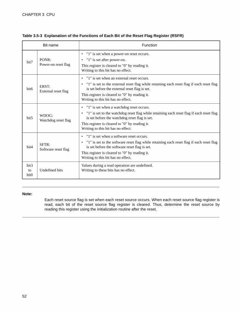
CHAPTER 3 CPU
Note:
Each reset source flag is set when each reset source occurs. When each reset source flag register isread, each bit of the reset source flag register is cleared. Thus, determine the reset source byreading this register using the initialization routine after the reset.
Table 3.5-3 Explanation of the Functions of Each Bit of the Reset Flag Register (RSFR)
Bit name Function
bit7PONR: Power-on reset flag
• "1" is set when a power-on reset occurs.
• "1" is set after power-on.
This register is cleared to "0" by reading it.Writing to this bit has no effect.
bit6ERST: External reset flag
• "1" is set when an external reset occurs.
• "1" is set to the external reset flag while retaining each reset flag if each reset flagis set before the external reset flag is set.
This register is cleared to "0" by reading it.Writing to this bit has no effect.
bit5WDOG: Watchdog reset flag
• "1" is set when a watchdog reset occurs.
• "1" is set to the watchdog reset flag while retaining each reset flag if each reset flagis set before the watchdog reset flag is set.
This register is cleared to "0" by reading it.Writing to this bit has no effect.
bit4SFTR: Software reset flag
• "1" is set when a software reset occurs.
• "1" is set to the software reset flag while retaining each reset flag if each reset flagis set before the software reset flag is set.
This register is cleared to "0" by reading it.Writing to this bit has no effect.
bit3to
bit0Undefined bits
Values during a read operation are undefined.Writing to these bits has no effect.
52

3.5.2 External Reset Pin
Inputting an "L" level to the external reset pin generates a reset. If products are set to with the reset output (optional), the pin outputs an "L" level depending on internal reset sources.
Block Diagram of External Reset PinThe external reset pin (RST) is a hysteresis input type and N-ch open-drain output type with a pull-up
resistor.
Figure 3.5-2 shows the block diagram of the external reset pin.
Figure 3.5-2 Block Diagram of External Reset Pin
Functions of External Reset PinInputting an "L" level to the external reset pin (RST) generates an internal reset signal.
The pin outputs an "L" level depending on internal reset sources or during the oscillation stabilization wait
time due to an external reset. Software reset, watchdog reset, and power-on reset are classed as internal
reset sources.
Note:
The external reset input accepts asynchronous with the internal clock. Therefore, initialization of theinternal circuit requires a clock. Especially when an external clock is used, a clock is needed to beinput at the reset.
P-ch
N-ch
RST
Pin
Pull-up resistor Approx. 50 kΩ/5.0V
Internal reset source
Input buffer
Internal reset signal
53
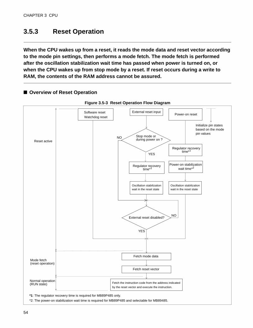
CHAPTER 3 CPU
3.5.3 Reset Operation
When the CPU wakes up from a reset, it reads the mode data and reset vector according to the mode pin settings, then performs a mode fetch. The mode fetch is performed after the oscillation stabilization wait time has passed when power is turned on, or when the CPU wakes up from stop mode by a reset. If reset occurs during a write to RAM, the contents of the RAM address cannot be assured.
Overview of Reset Operation
Figure 3.5-3 Reset Operation Flow Diagram
Reset active
Mode fetch (reset operation)
Normal operation (RUN state)
Software reset Watchdog reset
NO
NO
External reset input
YES
YES
Stop mode or
Oscillation stabilization wait in the reset state
External reset disabled?
Fetch mode data
Fetch reset vector
Fetch the instruction code from the address indicated
by the reset vector and execute the instruction.
Power-on reset
Oscillation stabilization wait in the reset state
Regulator recovery
Power-on stabilization
time*1
wait time*2Regulator recoverytime*1
during power on ?
*1: The regulator recovery time is required for MB89P485 only.
*2: The power-on stabilization wait time is required for MB89P485 and selectable for MB89485.
Initialize pin states based on the mode pin values
54
Mode PinsThe MB89480/480L series devices are single-chip mode devices. The mode pins (MODE) must be tied to
VSS.
Do not change the mode pin settings, even after the reset has been completed.
Mode FetchWhen the CPU wakes up from a reset, it reads the mode data and reset vector from internal ROM.
• Mode data (address: FFFDH)
Always set the mode data to "00H" (single-chip mode).
• Reset vector (address: FFFEH (upper), FFFFH (lower))
Contains the address where execution is to start after completion of the reset. The CPU starts executing
instructions from the address contained in the reset vector.
Oscillation Stabilization Wait in Reset StateThe reset operation for a power-on reset or external reset in stop mode starts after the main clock oscillation
stabilization wait time determined by the time-based timer. If the external reset input has not been released
when the wait time completes, the reset operation does not start until the external reset is released.
As the oscillation stabilization wait time is also required when an external clock is used, a reset requires
that the external clock is input.
The main clock oscillation stabilization wait time is made by the time-base timer.
Effect of Reset on RAM ContentsThe contents of RAM are unchanged before and after a reset other than power-on reset. If an external reset
is input close to a write timing, however, the contents of the write address cannot be assured. For this
reason, all RAM locations being used should be initialized following reset.
Regulator Recovery TimeMB89P485 contains an on-chip voltage regulator for the internal 3V circuits. In low-power consumption
mode or in the stop mode, the internal voltage regulator is turned off to minimize power dissipation. The
regulator recovery time is the time for the internal voltage regulator to resume normal operation.
The regulator recovery time is 20µs long, and it is required only in MB89P485.
Power-on Stabilization TimeWhen power-on, the on-chip voltage regulator requires a stabilization time in additional to the recovery
time. This additional wait time is called Power-on Stabilization Time. The external power supply voltage
must reach the minimum operation voltage within the Power-on stabilization time.
The Power-on Stabilization Time is required in MB89P485 and selectable by mask option in MB89485. It
depends on the oscillating clock, and it is 217/FCH long (FCH is the main clock operating frequency).
55

CHAPTER 3 CPU
*: specify by mask option.
Table 3.5-4 Regulator Recovery Time and Power-on Stabilization Time
Regulator Recovery Time Power-on Stabilization Time
MB89PV480 No No
MB89P485 Yes Yes
MB89485 No Selectable *
MB89P485L No No
MB89485L No No
56

3.5.4 Pin States during Reset
Reset initializes the pin states.
Pin States during ResetWhen a reset source occurs, with a few exceptions, all I/O pins (peripheral pins) go to the high-impedance
state and the mode data is read from internal ROM.
Pin States after Reading Mode DataWith a few exceptions, the I/O pins remain in the high-impedance state immediately after reading the mode
data.
Note:
For devices connected to pins that change to high-impedance state when a reset source occurs,take care that malfunction does not occur due to the change in the pin states.
Reference:
See "APPENDIX E MB89480/480L Series Pin States" for pin states at times other than a reset.
57

CHAPTER 3 CPU
3.6 Clocks
The clock generator is provided with an oscillator. By connecting with external resonator, circuits generate the high speed main clock source oscillation. Alternatively, externally generated clock inputs can be used.Clock controller controls the speed and supply of the clock signals according to the clock and standby modes.
Clock Supply MapOscillation of a clock and its supply to the CPU and peripheral circuit (peripheral functions) are controlled
by the clock controller. As shown in the map, operating clocks fed to the CPU and peripheral circuits are
affected by main clock/sub clock switching (clock mode), main clock speed switching (speed-shift
function), and standby modes (sleep/stop/watch).
Divided output derived from the free-run counter clocked by the peripheral circuit clock is supplied to the
peripheral functions.
Divided output from the time-base timer and watch prescaler are also supplied to the peripheral functions.
These clocks, however, are not affected by the speed-shift function, etc. The time-base timer is clocked by
the output of the main clock source oscillator after it is fed through a divide-by-n circuit, and the watch
prescaler is clocked directly by the sub clock oscillator. Figure 3.6-1 shows the clock supply map.
58
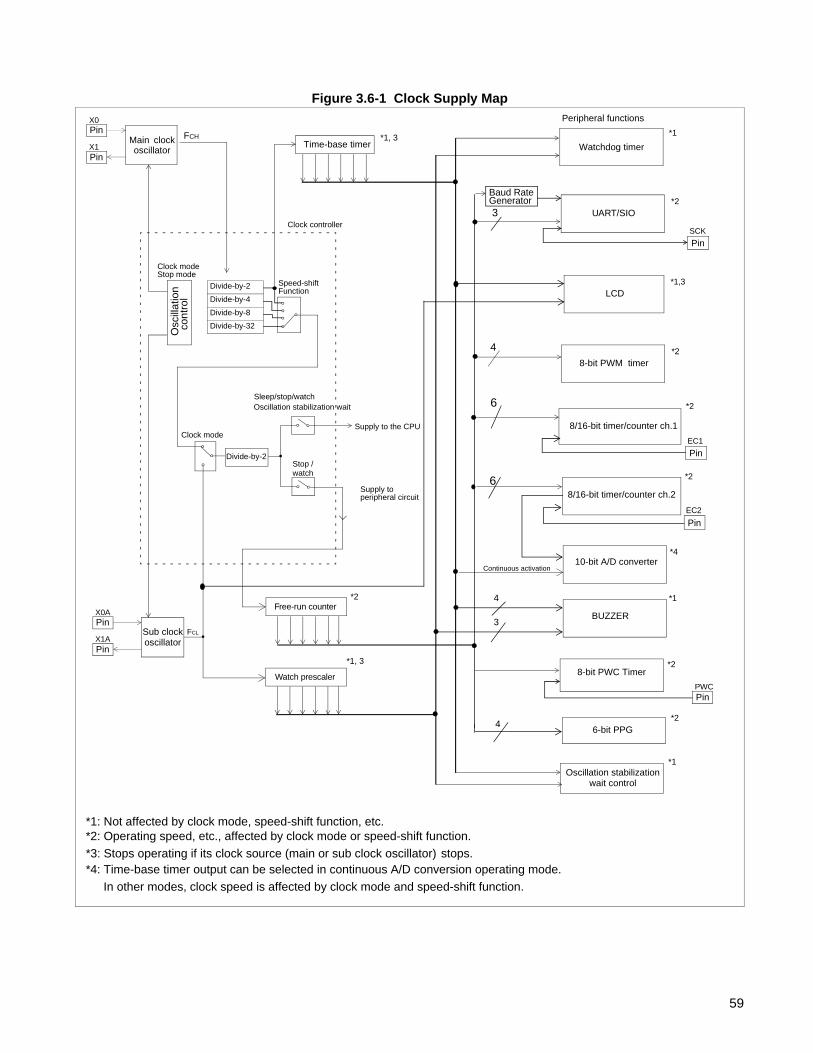
Figure 3.6-1 Clock Supply Map
8/16-bit timer/counter ch.1
Peripheral functions
Continuous activation
4
Time-base timer
Supply to the CPU
Clock controller
PinX1
PinX0
Osc
illat
ion
Watchdog timer
8-bit PWM timer
10-bit A/D converter
Main clockoscillator
FCH
Oscillation stabilization wait control
Watch prescaler
Free-run counter
PinX1A
PinX0A
Sub clockoscillator
Divide-by-2
FCL
Supply to peripheral circuit
con
trol
Divide-by-2
Divide-by-4
Divide-by-8
Divide-by-32
Sleep/stop/watchOscillation stabilization wait
Clock mode
Speed-shift Function
Clock modeStop mode
*1, 3
*2
*1, 3 *1
*2
*4
*1
*1: Not affected by clock mode, speed-shift function, etc.*2: Operating speed, etc., affected by clock mode or speed-shift function.
*3: Stops operating if its clock source (main or sub clock oscillator) stops.*4: Time-base timer output can be selected in continuous A/D conversion operating mode.
In other modes, clock speed is affected by clock mode and speed-shift function.
Stop / watch
UART/SIO *2
PinSCK
8-bit PWC Timer*2
PinPWC
Baud RateGenerator
LCD*1,3
PinEC2
PinEC1
8/16-bit timer/counter ch.2
3
6
6
BUZZER
4
3
6-bit PPG4
*2
*2
*1
*2
59
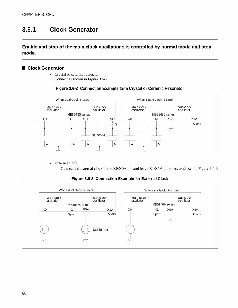
CHAPTER 3 CPU
3.6.1 Clock Generator
Enable and stop of the main clock oscillations is controlled by normal mode and stop mode.
Clock Generator• Crystal or ceramic resonator
Connect as shown in Figure 3.6-2
Figure 3.6-2 Connection Example for a Crystal or Ceramic Resonator
• External clock
Connect the external clock to the X0/X0A pin and leave X1/X1A pin open, as shown in Figure 3.6-3
Figure 3.6-3 Connection Example for External Clock
X0 X1
C C
Main clock
C C
oscillatorSub clockoscillator
MB89480 series
When dual clock is used
32.768 kHz
X0 X1
C C
Main clock
X0A
oscillatorSub clockoscillator
MB89480 series
When single clock is used
OpenR
X0A X1A X1A
X0 X1
Main clock
X1A
oscillatorSub clockoscillator
MB89480 series
X0 X1
Main clockoscillator
Sub clockoscillator
OpenOpenOpenOpen
32.768 kHz
X0A X0A X1A
When dual clock is used When single clock is used
MB89480 series
60
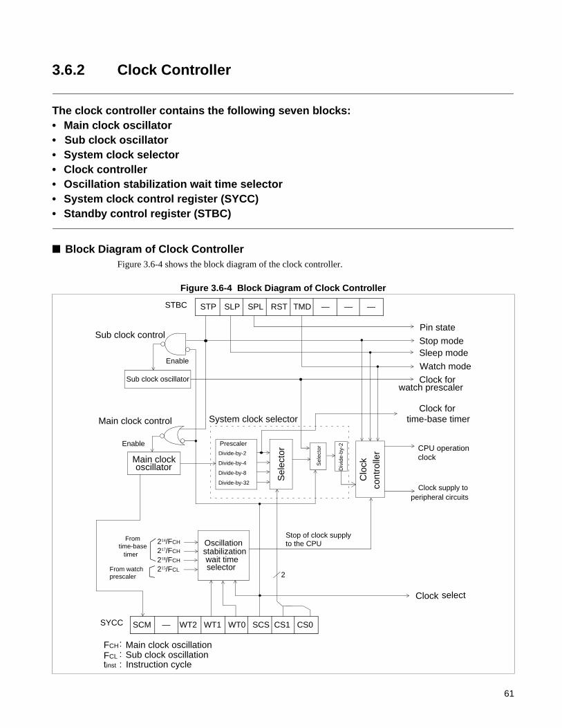
3.6.2 Clock Controller
The clock controller contains the following seven blocks:• Main clock oscillator• Sub clock oscillator• System clock selector• Clock controller• Oscillation stabilization wait time selector• System clock control register (SYCC)• Standby control register (STBC)
Block Diagram of Clock ControllerFigure 3.6-4 shows the block diagram of the clock controller.
Figure 3.6-4 Block Diagram of Clock Controller
Sub clock control
Enable
Sub clock oscillator
Pin state
Stop modeSleep mode
Watch mode
Clock forwatch prescaler
Clock for Main clock control System clock selector
Main clock oscillator
Enable Prescaler
Divide-by-2
Divide-by-4
Divide-by-8
Divide-by-32
Sel
ecto
r
Sel
ecto
r
Clo
ck
cont
rolle
r
Clock supply toperipheral circuits
From time-base Oscillation
stabilizationwait time selector
Stop of clock supply
Clock select
timer
FCH FCL :
:Sub clock oscillation
tinst : Instruction cycle
Main clock oscillation
CPU operation
time-base timer
214/FCH
217/FCH
218/FCH
215/FCL
SYCC SCM — WT2 WT1 WT0 SCS CS1 CS0
STBC STP SLP SPL RST TMD — — —STBC
2
SYCC
From watchprescaler
clock
Div
ide-
by-2
to the CPU
61

CHAPTER 3 CPU
Main clock oscillator
The main clock oscillator is stopped in main-stop mode.
Sub clock oscillator
The sub clock oscillator is normally running except in sub-stop mode.
System clock selector
The system clock selector selects one of four clocks: one of four divided clocks derived from the main
clock master clock oscillator.
Clock controller
This circuit controls the supply of operating clocks to the CPU and peripheral circuits, selecting the clock
based on the active mode: normal (RUN), or standby (sleep/stop/watch) mode.
Supply of the clock to the CPU is stopped until the clock supply stop signal in the oscillation stabilization
wait time selector is released.
Oscillation stabilization wait time selector
This register selector selects a wait time from among three main clock oscillation stabilization wait times
timed by the time-base timer oscillation stabilization time as the clock supply stop signal to the CPU based
on the normal mode, standby mode and reset.
System clock control register (SYCC)
The SYCC register is used to select the speed of the main clock, and the main clock oscillation stabilization
wait time, and to check the status of these selections.
Standby control register (STBC)
This register controls from normal operation (RUN) to the standby modes, sets the pin states in the stop
mode, and initiates software reset.
62

3.6.3 System Clock Control Register (SYCC)
The system clock control register (SYCC) controls main clock speed selection, and oscillation stabilization wait time selection.
Configuration of System Clock Control Register (SYCC)
Figure 3.6-5 Configuration of System Clock Control Register (SYCC)
Address bit7 bit6 bit5 bit4 bit3 bit2 bit1 bit0 Initial value
0007H SCM — WT2 WT1 WT0 SCS CS1 CS0 X-1MM100B
R R/W R/W R/W R/W R/W R/W
CS1 CS0
Main clock speed select bits
Instruction cycle(FCH = 12.5 MHz)
0 0 64/FCH (5.12µs)
0 1 16/FCH (1.28 µs)
1 0 8/FCH (0.64µs)
1 1 4/FCH (0.32µs)
SCS System clock select bit
0 Selects sub clock (32 kHz) mode
1 Selects main clock mode
WT1 WT0
Oscillation stabilization wait time select bit
Main clock oscillation stabilization wait time per selected time-base
timer output (FCH = 12.5MHz)
0 0 Reserved
0 1 Approx. 214/FCH (Approx. 1.3 ms)
1 0 Approx. 217/FCH (Approx. 10.5 ms)
1 1 Approx. 218/FCH (Approx. 21.0 ms)
WT2 Reserved bit
1 Always write "1"
SCM System clock monitor bit
0Sub clock (main clock stopped or in oscillation stabilization wait time)
1 Main clock
R/W : Readable/WritableR : Read only— : UndefinedX : Undefined valueM : Per option selection
: Initial value
FCH : Main clock oscillation (12.5MHz)
63

CHAPTER 3 CPU
Instruction Cycle (tinst)
Instruction cycle (minimum execution time) can be selected as 1/4, 1/8, 1/16, or 1/64 of the main clock.
The selection is made by main clock speed select bits (CS1 and CS0) of the SYCC register.
With main clock mode, and the highest clock speed selected (SYCC: SCS = 1, CS1 = 1, CS0 = 1), and with
a main clock source oscillation (FCH) of 12.5 MHz, the instruction cycle is 4/FCH = approximately 0.32 µs.
Table 3.6-1 Functions of Bits in System Clock Control Register (SYCC)
Bit name Function
bit7SCM: System clock monitor bit
• Indicates the current clock mode (operating clock).• "0" indicates sub clock mode (main clock is stopped or in the oscillation
stabilization wait time to go to main clock mode).• "1" indicates main clock mode.This is a read only bit. Writing to it has no effect on operation.
bit6 Undefined bit• The read value is undefined.• Writing to this bit has no effect on operation.
bit5WT2:Reserved bit
This bit must always write to "1".
bit4,bit3
WT1, WT0: Oscillation stabilization wait time select bits
• Select main clock oscillation stabilization wait time.• Selected wait time applies if external interrupt causes "wake up" from main-stop
mode (transition to normal (run) mode).Initial value of these bits is an option selection. Accordingly, when an oscillation stabilization wait time is provided at reset, the wait time will be as selected by the option.
Note:These bits should not be changed at the same time switching from sub clock to main clock (SCS = 1 -> 0). Before changing the bits, first check the SCM bit to verify that the device is not currently in the main clock oscillation stabilization wait time.
bit2SCS:System clock select bit
• Specifies the clock mode.• Writing "0" to this bit sets the CPU changing from main clock to sub clock mode.• Writing "1" to this bit causes the device to go from sub clock to main clock mode
after the oscillation stabilization wait time set by WT1 and WT0 bits.
bit1,bit0
CS1, CS0: Main clock speed select bits
• These bits select the clock speed for the main clock mode.• Four different speeds can be set for CPU and peripheral function operating clocks
(speed-shift function). However, the clock for the time-base timer is not affected by these bits.
64

3.6.4 Clock Modes
The clock modes consist of main clock mode and sub clock mode.In the main clock mode, the primary operating clock is provided by the main clock. The speed of the main clock is selected by switching between one of four clocks obtained by dividing the output of the main clock source oscillation (speed-shift function).In the sub clock mode, the main clock source oscillation is stopped, and operating clocks are provided solely by the sub clock.
Clock Mode Operating States
Reference:
See "3.7 Standby Modes (Low-Power Consumption)" for a description of the standby modes.
Table 3.6-2 Clock Mode Operating States
Clock mode
Main clock speedSYCC register
(SYCC: CS1, CS0)
Standby mode
Clock Oscillator Operating clocks for various sections Non-reset event
triggering except
standby mode
Main Sub CPUTime-base
timerPeripherals
Watch prescaler
Main clock mode
(1.1)
RUNOscillate
Oscillate
FCH/4FCH/2 FCH/4
FCL
IRQSleep
StopStop Stop Stop Stop
External interrupt
(1.0)
RUNOscillate
Oscillate
FCH/8FCH/2 FCH/8
FCL
IRQSleep
StopStop Stop Stop Stop
External interrupt
(0.1)
RUNOscillate
Oscillate
FCH/16FCH/2 FCH/16
FCL
IRQSleep
StopStop Stop Stop Stop
External interrupt
(0.0)
RUNOscillate
Oscillate
FCH/64FCH/2 FCH/64
FCL
IRQSleep
StopStop Stop Stop Stop
External interrupt
Sub clock mode
–
RUN
StopOscillate
FCL/2
Stop*FCL/2 FCL IRQ
SleepStop
Stop Stop Stop StopExternal interrupt
Watch Mode
Stop Oscillate Stop Stop* Stop FCL
External or watch interrupt
FCH: Main clock source oscillation (12.5MHz)
FCL: Sub clock source oscillation
* : Since the time-base timer runs on the main clock, it stops in sub clock mode.
Fast
Slow
65
CHAPTER 3 CPU
Speed-Shift (Main Clock Speed-switching) FunctionOne of four main clock frequencies can be selected by writing the appropriate values between "00B" and
"11B" to main clock speed select bits of the system clock control register (SYCC: CS1, CS0).
The switch-selected clock signal provides the operating clock for the CPU and peripheral circuits. The
time-base timer and watch prescaler, however, is not affected by the speed-shift (gear) function.
A slower main clock speed reduces power dissipation.
Operation of Main Clock ModeThe main clock and the sub clock oscillators both run in "main-run" mode (the normal main clock
operating mode). The watch prescaler runs on the sub clock, but the CPU, time-base timer, and other
peripheral circuits all use the main clock.
When operating in main clock mode, the speed-shift function can be used to select a main clock speed. This
selection affects all circuits that are clocked by the main clock except for the time-base timer. By
specifying a standby mode, you can also go to "main-sleep", or "main-stop" mode.
When the device is reset, the system always starts out in "main-run" mode regardless of how the reset was
initiated (Each operating mode exited by reset).
Changing from main clock mode to sub clock mode
Writing "0" to the system clock select bit in the system clock control register (SYCC:SCS) changes the
CPU from the main clock to sub clock mode. You can confirm which clock is currently being used by
reading the system clock monitor bit of the same register (SYCC: SCM).
Note:
If you go to sub clock mode immediately after power on, write the software so as to provide a longersub clock oscillation stabilization wait time than that defined by the watch prescaler.
Operation of Sub clock ModeIn the normal sub clock operating mode ("sub-run" mode), the system runs on the sub clock only. The main
clock oscillator is stopped. Using the low speed sub clock reduces power dissipation.
Other than the time-base timer, all functions operate the same in sub clock mode as they do in main clock
mode. If standby mode is specified while operating in sub clock mode, the device goes to "sub-sleep",
"sub-stop", or "watch" mode.
Returning to main clock mode from sub clock mode
Writing "1" to the system clock select bit in the system clock control register (SYCC:SCS) returns to main
clock mode from sub clock mode.
Operation from the main clock, however, will not start after the main clock oscillation stabilization wait
time has passed. One of four wait times can be selected by setting the oscillation stabilization wait time
select bits of the system clock control register (SYCC: WT1, WT0).
66
Note:
Do not change the oscillation stabilization wait time select bits (SYCC: WT1, WT0) at the same timeyou switch from sub clock to main clock mode (SYCC: SCS = 1), or during the oscillationstabilization wait time. Always check the system clock monitor bit to verify that the main clock is theactive operating clock (SYCC: SCM = 1) before changing these bits.
The device always enters the main clock oscillation stabilization wait time when the system is returned
from sub clock mode to main clock mode.
67

CHAPTER 3 CPU
3.6.5 Oscillation Stabilization Wait Time
When the system transitions to main-run mode from a state in which the main clock is stopped (such as at power-on, in main-stop and sub clock modes, etc.), a main clock oscillation stabilization time is required before operation starts.Similarly, a sub clock oscillation stabilization wait time is required when exiting the sub-stop mode, because the sub clock oscillation is stopped in that mode.
Oscillation Stabilization Wait TimeAfter starting, ceramic, crystal, and other resonators typically require the time between several milliseconds
and several tens of milliseconds to stabilize at their fixed oscillation frequency.
Therefore, operation of the CPU and other functions is disabled when oscillation first starts and no clock
signal is supplied to the CPU until the oscillation stabilization wait time has passed and the oscillation has
sufficiently stabilized.
The time required for oscillation to stabilize depends on the resonator type (crystal, ceramic, etc.)
connected to the clock generator. Consequently, it is necessary to select an oscillation stabilization wait
time that matches the type of oscillator being used.
Figure 3.6-6 shows the operation of an oscillator immediately after starting oscillation.
Figure 3.6-6 Operation of Oscillator immediately after Starting Oscillation
Regulator Recovery TimeMB89P485 contains an on-chip voltage regulator for the internal 3V circuits. In power-down mode or in
the stop mode, the internal voltage regulator stops the operation to minimize power dissipation. The
regulator recovery time is the time for the internal voltage regulator to resume normal operation.
The regulator recovery time is 20µs.
Power-on Stabilization Wait TimeWhen power-on, the on-chip voltage regulator requires a stabilization time in addition to the oscillation
stabilization time. This additional wait time is called power-on stabilization time. The external power
supply voltage must reach the minimum operation voltage within the power-on stabilization time.
The power-on stabilization time is required for MB89P485 and selectable by mask option in MB89485.
217/FCH of the power-on stabilization wait time is required (FCH is the main clock operating frequency).
Stabilization Wait Time for Different Operation for Different ProductTable 3.6-3 shows the operating states while waiting for the oscillation stabilization and the wait time in
each operation time.
Resonator oscillation time Oscillation stabilization wait time
Normal operation(wake-up from stop mode or reset operation)
Oscillation starts Oscillation stabilizes
68
Main Clock Oscillation Stabilization Wait TimeWhen first starting operation in main clock mode after a state in which the main clock oscillation is
stopped, an oscillation wait time for main clock is required. This wait time starts when the counter of the
time-base timer starts counting up from its cleared state, and ends when the count overflows at the specified
bit.
Oscillation stabilization wait time during operation
A time must be selected for the oscillation stabilization wait time when an external interrupt takes the
system from main-stop mode back to main-run mode, or when going from sub clock to main clock mode.
One of four possible wait times can be selected, using the oscillation stabilization wait time select bits of
the system clock control register (SYCC: WT1, WT0).
Oscillation stabilization wait time at reset
The oscillation stabilization wait time at reset (the initial values of WT1 and WT0) is selected as an option
setting.
Table 3.6-5 shows the relationship between the conditions in which main clock mode operation is started
and oscillation stabilization wait time.
Table 3.6-3 Operating States while Waiting Oscillation Stabilization Time
Operating Mode Oscillation CPUTime-based
TimerWatchdog
timerOther
PeripheralsPin
Cancel Method
Oscillation stabilization wait time Started
Halted
Operating Operating Operating
Hold* -Power-on stabilization wait time StartedHalted Halted Halted
Regulator recovery time Halted
*: During an oscillation stabilization wait time initiated by an external interrupt, pins go to their states immediately before stop mode. Pins go to their reset states during an oscillation stabilization wait time initiated by a reset.(See "3.5.3 Reset Operation".)
Table 3.6-4 Wait Time for Each Action
Operation MB89485 MB89P485 MB89PV480/P485L/485L
Power-on resetPower-on stabilization wait time (Selectable) + Oscillation stabilization wait time
Regulator recovery wait time + Power-on stab. wait time + Oscillation stabilization wait time
Oscillation stabilization wait time
External reset in stop/sub/clock mode or external interrupt trigger recovery from main stop mode
Oscillation stabilization wait time
Regulator recovery wait time + Oscillation stabilization wait time
Oscillation stabilization wait time
69

CHAPTER 3 CPU
Sub clock Oscillation Stabilization Wait TimeWhen an external interrupt returns the system from sub-stop (sub clock oscillation stopped) to sub-run
mode (thus starting the sub clock oscillation), a set sub clock oscillation stabilization wait time is provided.
(This set wait time is equal to 215/FCL, where FCL is the sub clock oscillator frequency.)
The sub clock oscillation stabilization wait time is also entered at power-on. Therefore, if you go to sub
clock mode after power on, you should insert a software wait, to provide a longer wait time before starting
this transition than the sub clock oscillation stabilization wait time.
The sub clock oscillation stabilization wait time starts when the watch prescaler starts counting up from the
cleared state, and ends when it overflows.
Table 3.6-5 Main Clock Mode Startup Conditions vs. Oscillation Stabilization Wait Time
Main clock mode startup
conditionsAt power-on
During sub clock mode Exit from main-stop mode Transition from sub clock to main clock mode (SYCC:
SCS*1=1)External reset
Software reset and watchdog
resetExternal reset
External interrupt
Oscillation stabilization wait time selection
Option setting SYCC: WT1, WT0*2
*1: System clock select bit of system clock control register *2: Oscillation stabilization wait time select bits of system clock control register
70
3.7 Standby Modes (Low-Power Consumption)
The standby modes consist of sleep mode, stop mode, and watch mode.From both main clock and sub clock modes, standby modes are changed to sleep mode, stop mode, or watch mode by setting the standby control register (STBC).From main clock mode, you can go only to sleep or stop mode, but from sub clock mode you can go any of the three standby modes. Standby mode reduces the power dissipation by stopping the operation of the CPU and peripheral functions.This section describes the relationship between standby mode and clock mode, and the operation of various sections during standby mode.
Standby ModesWatch mode reduce the power dissipation by lowering the frequencies of the clocks that run the CPU and
peripheral circuits. You can do this by switching from main clock to sub clock mode, or by using the speed-
shift function to select a lower main clock frequency. Standby modes reduce the power dissipation,
however, by stopping the clock signal supply to the CPU via clock controller (sleep mode), by stopping the
clock signal supply to the CPU and peripheral circuits (watch mode), or by stopping the source oscillation
itself (stop mode).
Main-sleep Mode
Main-sleep mode stops the operation of CPU and watchdog timer, but operate the peripheral functions
except watch prescaler by the main clock. (Certain functions can still run on the sub clock.)
Sub-sleep Mode
Sub-sleep mode stops the operation of main clock oscillator, CPU, watchdog timer, and time-base timer,
but operate the peripheral functions on the sub clock.
Main-stop Mode
Main-stop mode stops the operation of CPU and peripheral functions. The main clock oscillation is
stopped, but the sub clock oscillation keeps running. Everything is shut down except external interrupt
servicing, watch prescaler count operation, and some functions that operate from the sub clock.
Sub-stop Mode
Sub-stop mode stops all chip functions except the external interrupt, and stops the main clock and sub clock
oscillations.
Watch Mode
You can only go to watch mode from the sub clock mode. All functions are shut down except the watch
prescaler (watch interrupt), external interrupts, and some functions that operate from the sub clock.
71

CHAPTER 3 CPU
Note:
Even when the main clock is stopped, as it is in the main-stop and watch modes, as long as the subclock oscillation is still operating, some buzzer outputs and LCD controller/drivers will still operate.See "CHAPTER 16 BUZZER OUTPUT", "CHAPTER 17 LCD CONTROLLER/DRIVER", and theclock supply map provided in "3.6 Clocks" for details.
72

3.7.1 Operating States in Standby Modes
This section describes the operating states of the CPU and peripheral functions in standby modes.
Operating States in Standby Modes
Pin States in Standby Mode
Almost all I/O pins will either keep the state they were placed in by the pin state control bit of the standby
control register (STBC: SPL) just prior to going to the stop or watch mode, or will go to the high
impedance state. This is true regardless of the clock mode.
Reference:
See "APPENDIX E MB89480/480L Series Pin States" for pin states in a standby mode.
Table 3.7-1 Operating States of the CPU and Peripheral Functions in Standby Modes
FunctionMain clock mode Sub clock mode
RUN Sleep Stop RUN Sleep Stop Watch
Main clock Operating Operating Stop Stop Stop Stop Stop
Sub clock Operating Operating Operating Operating Operating Stop Operating
CPU
Instructions Operating Stop Stop Operating Stop Stop Stop
ROMOperating Hold Hold Operating Hold Hold Hold
RAM
I/O ports Operating Hold Hold Operating Hold Hold Hold
Peri
pher
al f
unct
ions
Watch prescaler Operating Operating Operating*1 Operating Operating Stop Operating
Time-base timer Operating Operating Stop Stop Stop Stop Stop
8/16-bit timer/counter 11, 12, 21, 22
Operating Operating Stop Operating Operating Stop Stop
UART/SIO Operating Operating Stop Operating Operating Stop Stop
8-bit PWM timers Operating Operating Stop Operating Operating Stop Stop
A/D converter Operating Operating Stop Operating Operating Stop Stop
External Interrupts1 and 2
Operating Operating Operating Operating Operating Operating Operating
6-bit PPG Operating Operating Stop Operating Operating Stop Stop
Watchdog timer Operating Stop Stop Operating*2 Stop Stop Stop
PWC timer Operating Operating Stop Operating Operating Stop Stop
6-bit PPG Operating Operating Stop Operating Operating Stop Stop
A/D convertor Operating Operating Stop Operating Operating Stop Stop
BUZZER Operating Operating Operating*2 Operating*2 Operating*2 Stop Operating*2
LCD controller/driver Operating Operating Operating*3 Operating*3 Operating*3 Stop*4 Operating*3
*1: Watch prescaler counts but does not generate watch interrupts.*2: Can be operated if watch prescaler output is selected as its operating clock.*3: If the sub clock is selected as the operating clock, in watch mode, LCD controller/driver operation must be enabled.*4: In devices with on-chip voltage boosters (MB89480 series), the voltage booster stops operating.
73
CHAPTER 3 CPU
3.7.2 Sleep Mode
This section describes the operations of sleep mode.
Operation of Sleep Mode
Changing to sleep mode
Sleep mode stops the CPU operating clock. The CPU stops while maintaining all register contents and
RAM contents, at their values immediately prior to entering sleep mode. However, peripheral functions
except the watchdog timer continue to operate.
Writing "1" to the sleep bit in the standby control register (STBC: SLP) changes the CPU to sleep mode. If
an interrupt request is generated when "1" is written to the SLP bit, the write to the bit is ignored, and the
CPU continues the instruction execution without change to sleep mode. (The CPU does not change to sleep
mode even after completion of the interrupt processing.)
Wake-up from sleep mode
A reset or an interrupt from a peripheral function wakes up the CPU from sleep mode.
The reset operation also initializes the pin states.
If an interrupt request with an interrupt level higher than "11B" occurs from a peripheral function or an
external interrupt circuit during sleep mode, the CPU wakes up from sleep mode, regardless of the interrupt
enable flag (CCR: I) and interrupt level bits (CCR: IL1 and IL0) in the CPU.
The normal interrupt operation is performed after wake-up from sleep mode. If the interrupt request is
accepted, the CPU executes interrupt processing. If the interrupt request is not accepted, the CPU continues
execution from the subsequent instruction following the instruction executed immediately before changing
to sleep mode.
74

3.7.3 Stop Mode
This section describes the operations of stop mode.
Operation of Stop Mode
Changing to stop mode
Stop mode stops the source oscillation. Most functions stop while maintaining all register and RAM
contents at their value immediately before changing to stop mode.
If the system is in main clock mode, the main clock oscillation stops. Except the external interrupt circuit,
however, the CPU and other peripheral functions stop operating.
Writing "1" to the stop bit in the standby control register (STBC: STP) changes the CPU to stop mode. At
this time, external pin states are held if the pin state specification bit (STBC: SPL) is "0". If SPL is "1",
external pins go to the high-impedance state. (Pins with the pull-up resistor go to the "H" level.)
If an interrupt request is generated when "1" is written to the STP bit, the write to the bit is ignored, and the
CPU continues the instruction execution without change to stop mode. (The CPU does not change to stop
mode even after completion of the interrupt processing.)
Prohibit interrupt request output from the time-base timer (TBTC: TBIE = 0) before changing to stop mode
in main clock mode as necessary.
Wake-up from stop mode
A reset or an external interrupt wakes up the CPU from stop mode.
If reset occurs during stop mode on a product, the reset operation starts after the main clock oscillation
stabilization wait time. The reset initializes pin states.
If an interrupt request with an interrupt level higher than "11B" occurs from an external interrupt circuit
during stop mode, the CPU wakes up from stop mode, regardless of the interrupt enable flag (CCR: I) and
interrupt level bits (CCR: IL1, IL0) in the CPU. Only external interrupt requests can occur during stop
mode because peripheral functions are stopped.
After wake-up from stop mode, the normal interrupt operation is performed after the oscillation
stabilization wait time has passed. If the interrupt request is accepted, the CPU executes interrupt
processing. If the interrupt request is not accepted, the CPU continues execution from the subsequent
instruction following the instruction executed immediately before entering stop mode.
Some peripheral functions restart from mid-operation when the CPU wakes up from stop mode by an
external interrupt. The first interval time from the interval timer function, for example, is undefined.
Therefore, initialize all peripheral functions after wake-up from stop mode.
Note:
Only interrupt requests from external interrupt circuits can be used to wake up from stop mode by aninterrupt.
75

CHAPTER 3 CPU
3.7.4 Watch Mode
This section describes the operations of watch mode.
Operation of watch Mode
Changing to watch mode
Watch mode stops the clocks that clock the CPU and the main peripheral circuit. You can go to watch
mode only from sub clock mode (in which the main clock oscillation is stopped).
Prior to going to watch mode, registers are saved and the contents of RAM are held. All chip functions
other than watch prescaler (watch interrupt), external interrupt circuit, and certain functions that run off of
the sub clock stop. Accordingly, data can be held with extremely small power dissipation.
Writing "1" to the watch bit in the standby control register (STBC: TMD) changes the CPU to watch mode.
This can be done, however, only when the system clock select bit of the system clock control register
(SYCC: SCS) is "0" (sub clock mode active).
When you go to watch mode, external pin states are held if the pin state specification bit in the standby
control register (STBC: SPL) is "0". If SPL is "1", external pins go the high-impedance state. (Pins with a
pull-up resistor (optional) go to the "H" level)
If an interrupt request is generated when "1" is written to the TMD bit, the write to the bit is ignored, and
the CPU continues the instruction execution without change to watch mode. (The CPU does not change to
watch mode even after completion of the interrupt processing.)
Wake-up from watch mode
A reset, a watch interrupt or an external interrupt wakes up CPU from watch mode.
If a reset occurs during watch mode on a product with power-on reset, the reset operation starts after the
main clock oscillation stabilization wait time.
Products without power-on reset, do not require for the oscillation stabilization wait time after a reset in
watch mode.
The reset initializes pin states.
If an interrupt request with an interrupt level higher than "11B" occurs from a watch prescaler or an external
interrupt circuit during watch mode, the CPU wakes up from watch mode, regardless of the interrupt enable
flag (CCR:I) and interrupt level bits (CCR: IL1, IL0) in the CPU. Only watch interrupt or external interrupt
requests can occur during watch mode because most of the peripheral functions except watch prescaler are
stopped.
After wake-up from stop mode, the normal interrupt operation is performed. If the interrupt request is
accepted, the CPU executes interrupt processing. If the interrupt request is not accepted, the CPU continues
execution from the subsequent instruction following the instruction executed immediately before entering
watch mode.
Some peripheral functions restart from mid-operation when the CPU wakes up from watch mode. The first
interval time from the interval timer function, for example, is undefined. Therefore, initialize all peripheral
functions after wake-up from watch mode.
76

3.7.5 Standby Control Register (STBC)
The standby control register (STBC) controls the changing to sleep mode or stop mode, sets the pin states in stop mode, and initiates software resets.
Standby Control Register (STBC)
Figure 3.7-1 Standby Control Register (STBC)
Address bit7 bit6 bit5 bit4 bit3 bit2 bit1 bit0 Initial value0008H STP SLP SPL RST TMD — — — 00010---B
R/W R/W R/W W R/W
TMD
Watch bit
Valid only in sub clock mode (SYCC: SCS = 0)
Read Write
0Reading always returns "0".
No effect on operation
1 — Changing to watch mode
RSTSoftware reset bit
Read Write
0 —Generates a reset signal for four instruction cycles.
1Reading always returns "1".
No effect on operation
SPLPin state specification bit
Read Write
0External pins hold their states prior to entering stop mode or watch mode.
1External pins go to high-impedance state on entering stop mode or watch mode.
SLPSleep bit
Read Write
0Reading always returns "0".
No effect on operation
1 — Change to sleep mode.
STPStop bit
Read Write
0Reading always returns "0".
No effect on operation
1 — Change to stop mode.R/W : Readable/Writable
W : Write only
— : Undefined
: Initial value
77

CHAPTER 3 CPU
Table 3.7-2 Functions of Bits in Standby Control Register (STBC)
Bit name Function
bit7STP: Stop bit
Sets the CPU changing to stop mode.Writing "1" to this bit sets the CPU changing to stop mode.Writing "0" to this bit has no effect on operation.Reading this bit always returns "0".
bit6SLP:Sleep bit
Sets the CPU changing to sleep mode.Writing "1" to this bit sets the CPU changing to sleep mode.Writing "0" to this bit has no effect on operation.Reading this bit always returns "0".
bit5SPL: Pin state specification bit
Specifies the states of the external pins during stop mode and watch mode.Writing "1" to this bit specifies that external pins to go to high impedance state on entering stop mode or watch mode. (Pin with a pull-up resistor go to "H" level.)Writing "0" to this bit specifies that external pin hold their states (levels) on changing to stop mode or watch mode.Reading this bit always returns "0".
bit4RST: Software reset bit
Specifies a software reset.Writing "1" to this bit has no effect on operation.Writing "0" to this bit generates an internal reset source for four instruction cycles.Reading this bit always returns "1".
bit3TMD: Watch bit
Sets the CPU changing to watch mode.A write to this bit is valid only in sub clock mode (SYCC:SCS=0).Writing "1" to this bit sets the CPU changing to watch mode.Writing "0" to this bit has no effect on operation.Reading this bit always returns "0".
bit2to
bit0Undefined bits
The read value is undefined.Writing to these bits has no effect on operation.
78
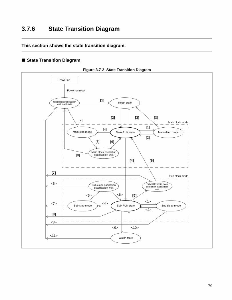
3.7.6 State Transition Diagram
This section shows the state transition diagram.
State Transition Diagram
Figure 3.7-2 State Transition Diagram
Power on
Oscillation stabilization wait reset state
Sub-RUN state
Reset state
Power-on reset
Main-stop mode Main-RUN state Main-sleep mode
Main clock mode
Main clock oscillation stabilization wait
Sub clock oscillation stabilization wait
Sub clock mode
Sub-RUN main clock oscillation stabilization
wait
Sub-stop mode Sub-sleep mode
Watch state<11>
<3>
<8>
[8]
<7>
[7]
[1]
[2] [3] [3]
[2]
[1]
[8]
[5] [6]
[4] [6]
[5]
<1>
<2>
<4>
<5> <6>
<9> <10>
[7]
[4]
79
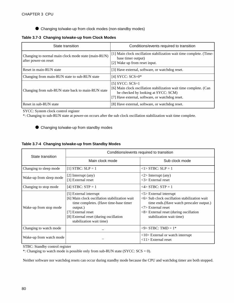
CHAPTER 3 CPU
Changing to/wake-up from clock modes (non-standby modes)
Changing to/wake-up from standby modes
Table 3.7-3 Changing to/wake-up from Clock Modes
State transition Conditions/events required to transition
Changing to normal main clock mode state (main-RUN) after power-on reset
[1] Main clock oscillation stabilization wait time complete. (Time-base timer output)
[2] Wake up from reset input.
Reset in main-RUN state [3] Have external, software, or watchdog reset.
Changing from main-RUN state to sub-RUN state [4] SYCC: SCS=0*
Changing from sub-RUN state back to main-RUN state
[5] SYCC: SCS=1[6] Main clock oscillation stabilization wait time complete. (Can
be checked by looking at SYCC: SCM)[7] Have external, software, or watchdog reset.
Reset in sub-RUN state [8] Have external, software, or watchdog reset.
SYCC: System clock control register*: Changing to sub-RUN state at power-on occurs after the sub clock oscillation stabilization wait time complete.
Table 3.7-4 Changing to/wake-up from Standby Modes
State transitionConditions/events required to transition
Main clock mode Sub clock mode
Changing to sleep mode [1] STBC: SLP = 1 <1> STBC: SLP = 1
Wake-up from sleep mode[2] Interrupt (any)[3] External reset
<2> Interrupt (any)<3> External reset
Changing to stop mode [4] STBC: STP = 1 <4> STBC: STP = 1
Wake-up from stop mode
[5] External interrupt[6] Main clock oscillation stabilization wait
time completes. (Have time-base timer output.)
[7] External reset[8] External reset (during oscillation
stabilization wait time)
<5> External interrupt<6> Sub clock oscillation stabilization wait
time ends.(Have watch prescaler output.)<7> External reset<8> External reset (during oscillation
stabilization wait time)
Changing to watch mode _ <9> STBC: TMD = 1*
Wake-up from watch mode _<10> External or watch interrupt<11> External reset
STBC: Standby control register*: Changing to watch mode is possible only from sub-RUN state (SYCC: SCS = 0).
Neither software nor watchdog resets can occur during standby mode because the CPU and watchdog timer are both stopped.
80
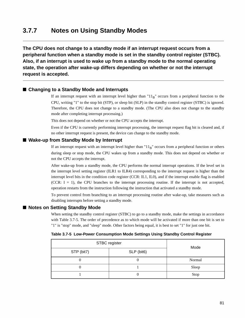
3.7.7 Notes on Using Standby Modes
The CPU does not change to a standby mode if an interrupt request occurs from a peripheral function when a standby mode is set in the standby control register (STBC). Also, if an interrupt is used to wake up from a standby mode to the normal operating state, the operation after wake-up differs depending on whether or not the interrupt request is accepted.
Changing to a Standby Mode and InterruptsIf an interrupt request with an interrupt level higher than "11B" occurs from a peripheral function to the
CPU, writing "1" to the stop bit (STP), or sleep bit (SLP) in the standby control register (STBC) is ignored.
Therefore, the CPU does not change to a standby mode. (The CPU also does not change to the standby
mode after completing interrupt processing.)
This does not depend on whether or not the CPU accepts the interrupt.
Even if the CPU is currently performing interrupt processing, the interrupt request flag bit is cleared and, if
no other interrupt request is present, the device can change to the standby mode.
Wake-up from Standby Mode by InterruptIf an interrupt request with an interrupt level higher than "11B" occurs from a peripheral function or others
during sleep or stop mode, the CPU wakes up from a standby mode. This does not depend on whether or
not the CPU accepts the interrupt.
After wake-up from a standby mode, the CPU performs the normal interrupt operations. If the level set in
the interrupt level setting register (ILR1 to ILR4) corresponding to the interrupt request is higher than the
interrupt level bits in the condition code register (CCR: IL1, IL0), and if the interrupt enable flag is enabled
(CCR: I = 1), the CPU branches to the interrupt processing routine. If the interrupt is not accepted,
operation restarts from the instruction following the instruction that activated a standby mode.
To prevent control from branching to an interrupt processing routine after wake-up, take measures such as
disabling interrupts before setting a standby mode.
Notes on Setting Standby ModeWhen setting the standby control register (STBC) to go to a standby mode, make the settings in accordance
with Table 3.7-5. The order of precedence as to which mode will be activated if more than one bit is set to
"1" is "stop" mode, and "sleep" mode. Other factors being equal, it is best to set "1" for just one bit.
Table 3.7-5 Low-Power Consumption Mode Settings Using Standby Control Register
STBC registerMode
STP (bit7) SLP (bit6)
0 0 Normal
0 1 Sleep
1 0 Stop
81

CHAPTER 3 CPU
Oscillation Stabilization Wait TimeAs the oscillator that provides the source oscillation is stopped during stop mode in both main clock mode,
a wait time is required for oscillation to stabilize after the oscillator restarts operation.
In main clock mode, the main clock oscillation stabilization wait time is selected from one of three possible
wait times defined by the time-base timer.
In main clock mode, if the interval time set for the time-base timer is less than the oscillation stabilization
wait time, the time-base timer generates an interval timer interrupt request before the end of the oscillation
stabilization wait time. To prevent this, disable the interrupt request output for the time-base timer (TBTC:
TBIE = 0) before changing to stop mode in main clock mode as necessary.
82
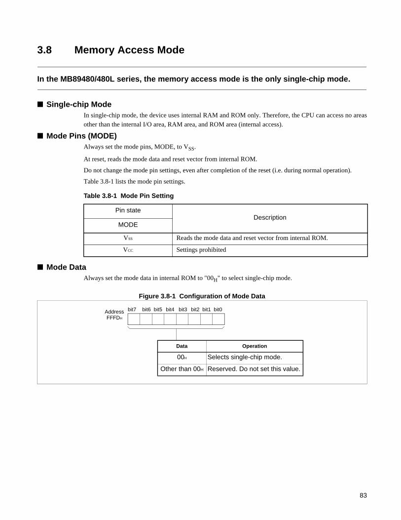
3.8 Memory Access Mode
In the MB89480/480L series, the memory access mode is the only single-chip mode.
Single-chip ModeIn single-chip mode, the device uses internal RAM and ROM only. Therefore, the CPU can access no areas
other than the internal I/O area, RAM area, and ROM area (internal access).
Mode Pins (MODE)Always set the mode pins, MODE, to VSS.
At reset, reads the mode data and reset vector from internal ROM.
Do not change the mode pin settings, even after completion of the reset (i.e. during normal operation).
Table 3.8-1 lists the mode pin settings.
Mode DataAlways set the mode data in internal ROM to "00H" to select single-chip mode.
Figure 3.8-1 Configuration of Mode Data
Table 3.8-1 Mode Pin Setting
Pin stateDescription
MODE
VSS Reads the mode data and reset vector from internal ROM.
VCC Settings prohibited
bit7 bit6 bit5 bit4 bit3 bit2 bit1 bit0AddressFFFDH
Data Operation
00H Selects single-chip mode.
Other than 00H Reserved. Do not set this value.
83
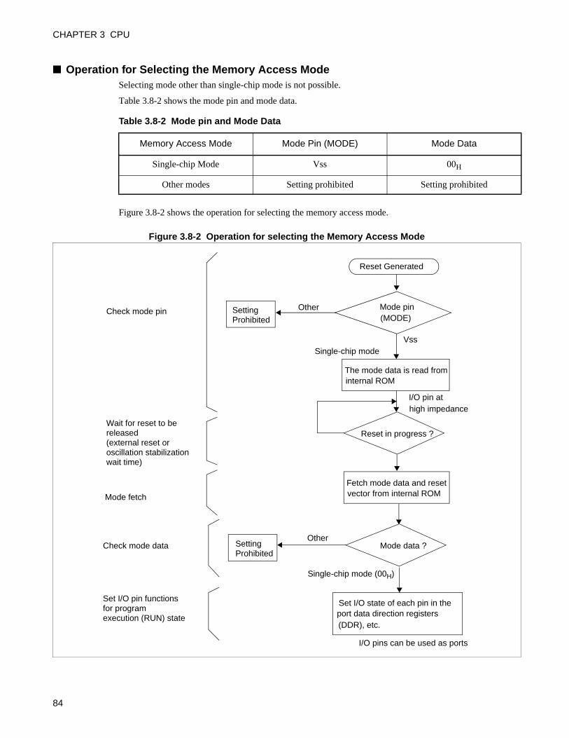
CHAPTER 3 CPU
Operation for Selecting the Memory Access ModeSelecting mode other than single-chip mode is not possible.
Table 3.8-2 shows the mode pin and mode data.
Figure 3.8-2 shows the operation for selecting the memory access mode.
Figure 3.8-2 Operation for selecting the Memory Access Mode
Table 3.8-2 Mode pin and Mode Data
Memory Access Mode Mode Pin (MODE) Mode Data
Single-chip Mode Vss 00H
Other modes Setting prohibited Setting prohibited
Reset Generated
Mode pin
The mode data is read frominternal ROM
Reset in progress ?
Fetch mode data and resetvector from internal ROM
Mode data ?
Set I/O state of each pin in theport data direction registers(DDR), etc.
VssSingle-chip mode
I/O pin at high impedance
Single-chip mode (00H)
I/O pins can be used as ports
SettingProhibited
SettingProhibited
Other
Other
Check mode pin
Wait for reset to bereleased(external reset oroscillation stabilizationwait time)
Mode fetch
Check mode data
Set I/O pin functionsfor programexecution (RUN) state
(MODE)
84

CHAPTER 4I/O PORTS
This chapter describes the functions and operation of the I/O ports.
4.1 Overview of I/O Ports
4.2 Port 0
4.3 Port 1
4.4 Port 2
4.5 Port 3
4.6 Port 4
4.7 Port 5
4.8 Program Example for I/O Ports
85

CHAPTER 4 I/O PORTS
4.1 Overview of I/O Ports
The I/O ports consist of 42 pins general-purpose I/O ports.The ports also serve as peripherals (I/O pins of peripheral functions).
Functions of I/O PortThe functions of the I/O ports are to output data from the CPU via the I/O pins and to fetch signals input to
the I/O pins into the CPU. Input and output are performed via the port data registers (PDR). Also, for
certain ports the direction of each I/O pin can be individually set to either input or output for each bit by the
port direction register (DDR).
The following lists the functions of each port and the peripheral with which the ports also serve as.
• Port 0: General-purpose I/O port. Also serves as peripherals
(INT20 to INT27, PWC, PPG, BUZ, EC2*1, TO2*1)
• Port 1: General-purpose I/O port. Also serves as peripherals
(AN0 to AN3, INT10 to INT13, SEG23 to SEG26, SEG27 to SEG30*2)
• Port 2: General-purpose I/O port. Also serves as peripherals
(C0, C1, V1, V2, PWM, SCK, SO, SI, EC1, TO1, EC2*2, TO2*2)
• Port 3: General-purpose N-channel open-drain output port. Also serves as peripherals
(COM2, COM3)
• Port 4: General-purpose I/O port. Also serves as peripherals
(SEG8 to SEG15)
• Port 5: General-purpose I/O port. Also serves as peripherals (except for P57, which is general-purpose
input port only)
(SEG16 to SEG22)
*1: When built-in booster is selected.
*2: When built-in booster is not selected.
86

Table 4.1-1 lists the functions of each port and Table 4.1-2 lists the registers for each port.
Table 4.1-1 Port Functions
Port Pin nameInputtype
Output type
Function bit7 bit6 bit5 bit4 bit3 bit2 bit1 bit0
Port0
P00/INT20 to
P07/INT27/BUZ
CMOS(resource
hysteresis)
CMOS push-pull
General purpose I/O port
P07 P06 P05 P04 P03 P02 P01 P00
External Interrupts 2 INT27 INT26 INT25 INT24 INT23 INT22 INT21 INT20
Peripherals BUZ PPG PWC TO2*1 EC2*1 — — —
Port1
P10/SEG23/INT10
toP17/SEG30/
AN3
N-ch open-drain (resource hysteresis/
analog)
N-ch open-drain
General purpose I/O port
P17 P16 P15 P14 P13 P12 P11 P10
LCD segment output SEG30*2 SEG29*2 SEG28*2 SEG27*2 SEG26 SEG25 SEG24 SEG23
Analog input/ External interrupts 1
AN3 AN2 AN1 AN0 INT13 INT12 INT11 INT10
Port2
P20/PWM to
P23/SI
CMOS (resource
hysteresis)
CMOS push-pull
General purpose I/O port
P27 P26 P25 P24 P23 P22 P21 P20
P24/C1/TO2to
P27/V2/EC1
N-ch open-drain (resource
hysteresis)
N-ch open-drain
LCD driver V2 V1 C0*1 C1*1 — — — —
Peripherals EC1 TO1 EC2*2 TO2*2 SI SO SCK PWM
Port3P30/COM2
toP31/COM3
—N-ch open-drain
Output only port — — — — — — P31 P30
LCD common output — — — — — — COM3 COM2
Port4P40/SEG8
toP47/SEG15
CMOSN-ch open-drain
General purpose I/O port
P47 P46 P45 P44 P43 P42 P41 P40
LCD segment output SEG15 SEG14 SEG13 SEG12 SEG11 SEG10 SEG9 SEG8
Port5P50/SEG22
to P57
CMOSN-ch open-drain
General purpose I/O port P57*3 P56 P55 P54 P53 P52 P51 P50
LCD segment output — SEG22 SEG21 SEG20 SEG19 SEG18 SEG17 SEG16
*1: When built-in booster is selected.*2: When built-in booster is not selected.*3: Input only
Table 4.1-2 Port Registers
Register Read/Write Address Initial value
Port 0 data register (PDR0) R/W 0000H XXXXXXXXB
Port 0 data direction register (DDR0) W* 0001H 00000000B
Port 0 pull-up resistor control register (PURC0) R/W 0070H 11111111B
Port 1 data register (PDR1) R/W 0002H XXXXXXXXB
Port 1 data direction register (DDR1) W* 0003H 00000000B
A/D input enable register (ADER) R/W 0030H 1111----B
Port 2 data register (PDR2) R/W 0004H 00000000B
Port 2 data direction register (DDR2) R/W 0006H 00000000B
Port 2 pull-up resistor control register (PURC2) R/W 0072H ----1111B
Port 3 data register (PDR3) R/W 000CH ------11B
Port 4 data register (PDR4) R/W 0010H 11111111B
Port 5 data register (PDR5) R/W 0012H X1111111B
* : Bit manipulation instructions cannot be used on DDR0, DDR1.R/W: Readable/Writable R: Read onlyW: Write only X: Undefined value -: Unused pin
87
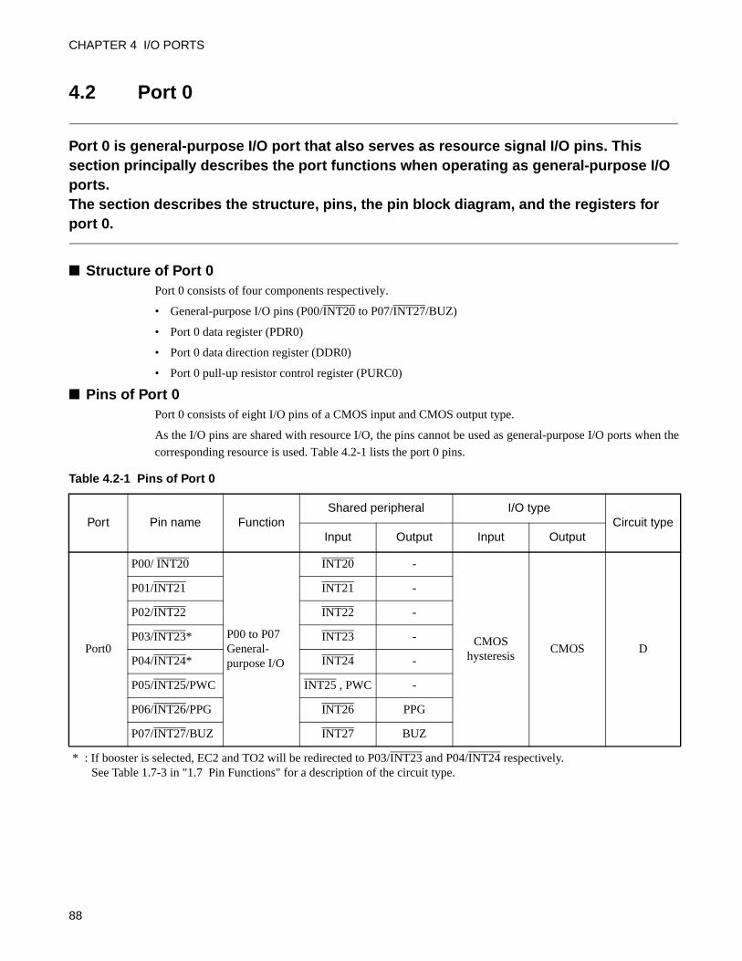
CHAPTER 4 I/O PORTS
4.2 Port 0
Port 0 is general-purpose I/O port that also serves as resource signal I/O pins. This section principally describes the port functions when operating as general-purpose I/O ports.The section describes the structure, pins, the pin block diagram, and the registers for port 0.
Structure of Port 0Port 0 consists of four components respectively.
• General-purpose I/O pins (P00/INT20 to P07/INT27/BUZ)
• Port 0 data register (PDR0)
• Port 0 data direction register (DDR0)
• Port 0 pull-up resistor control register (PURC0)
Pins of Port 0Port 0 consists of eight I/O pins of a CMOS input and CMOS output type.
As the I/O pins are shared with resource I/O, the pins cannot be used as general-purpose I/O ports when the
corresponding resource is used. Table 4.2-1 lists the port 0 pins.
Table 4.2-1 Pins of Port 0
Port Pin name FunctionShared peripheral I/O type
Circuit typeInput Output Input Output
Port0
P00/ INT20
P00 to P07General-purpose I/O
INT20 -
CMOShysteresis
CMOS D
P01/INT21 INT21 -
P02/INT22 INT22 -
P03/INT23* INT23 -
P04/INT24* INT24 -
P05/INT25/PWC INT25 , PWC -
P06/INT26/PPG INT26 PPG
P07/INT27/BUZ INT27 BUZ
* : If booster is selected, EC2 and TO2 will be redirected to P03/INT23 and P04/INT24 respectively.See Table 1.7-3 in "1.7 Pin Functions" for a description of the circuit type.
88
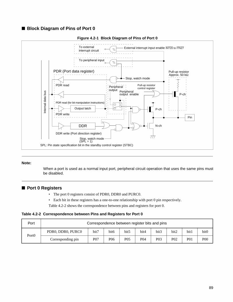
Block Diagram of Pins of Port 0
Figure 4.2-1 Block Diagram of Pins of Port 0
Note:
When a port is used as a normal input port, peripheral circuit operation that uses the same pins mustbe disabled.
Port 0 Registers• The port 0 registers consist of PDR0, DDR0 and PURC0.
• Each bit in these registers has a one-to-one relationship with port 0 pin respectively.
Table 4.2-2 shows the correspondence between pins and registers for port 0.
DDR
Inte
rnal
dat
a bu
s
PDR read
PDR read (for bit manipulation instructions)
PDR write
Pull-up resistorApprox. 50 kΩ
Pin
SPL: Pin state specification bit in the standby control register (STBC)
N-ch
P-ch
P-ch
Stop, watch mode
Output latch
To external interrupt circuit
Stop, watch mode
To peripheral input
DDR write (Port direction register)
Pull-up resistor control register
PDR (Port data register)
(SPL = 1)
Peripheral output
External interrupt input enable INT20 to ITN27
output enablePeripheral
Table 4.2-2 Correspondence between Pins and Registers for Port 0
Port Correspondence between register bits and pins
Port0PDR0, DDR0, PURC0 bit7 bit6 bit5 bit4 bit3 bit2 bit1 bit0
Corresponding pin P07 P06 P05 P04 P03 P02 P01 P00
89
CHAPTER 4 I/O PORTS
4.2.1 Port 0 Registers (PDR0, DDR0, RDR0)
This section describes the port 0 registers.
Functions of Port 0 Register
Port 0 data register (PDR0)
The PDR0 register holds the pin states. Therefore, a bit corresponding to a pin set as an output port can
be read as the same state ("0" or "1") as the output latch, but when it is an input port, it cannot be read as
the output latch state.
Reference:
For bit manipulation instructions (SETB and CLRB), since the state of output latch (not the pin) isread, the output latch states of bits other than those being operated on are not changed.
Port 0 direction register (DDR0)
The DDR0 register sets the direction (input or output) for each pin (bit).
Setting "1" to the bit corresponding to a port (pin) sets the pin as an output port. Setting "0" sets the pin
as an input port.
Note:
As the DDR0 register is write only, the bit manipulation instructions (SETB and CLRB) cannot beused.
Settings as peripheral output
To use a peripheral that has an output pin, set the peripheral output enable bit for that pin to the "enable"
state. As can be seen in the block diagram, the peripheral has precedence over the general-purpose port
for use of the output pin. Once the peripheral output is enabled, the states set in the PDR0 and DDR0
registers are no longer valid, and do not affect the data output by the peripheral, or the enabling of the
output.
Settings as a peripheral input
To use a peripheral that has a port 0 pin as an input pin, set that pin as an input port. The output latch
data for that pin will no longer be valid.
90

Table 4.2-3 lists the functions of the port 0 registers.
Port 0 pull-up resistor control register (PURC0)
By using pull-up resistor control register (PURC0), it is possible to turn on/off pull-up resistor.
When pull-up resistor is selected in pull-up resistor control register, the states of these pins in stop mode
(SPL=1) are in "H" level (pull-up state) rather than high impedance. However, during reset, pull-up is
unavailable and will be in high impedance state.
Figure 4.2-2 lists the setting of Port 0 pull-up resistor control register.
Figure 4.2-2 Pull-up resistor control register setting (PURC0)
Table 4.2-3 Functions of Port 0 Registers
Register Data Read WriteRead/Write
Address Initial value
Port 0 data register (PDR0)
0 Pin state is the "L" level.Sets "0" to the output latch.Outputs an "L" level to the pin if the pin functions as an output port.
R/W 0000H XXXXXXXXB
1 Pin state is the "H" level.Sets "1" to the output latch.Outputs an "H" level to the pin if the pin functions as an output port.
Port 0 data direction register (DDR0)
0 Reading is not permitted (write only).
Disables output transistor and sets the pin as an input pin.
W 0001H 00000000B
1Enables output transistor and sets the pin as output pin.
R/W: Readable/WritableW : Write onlyX : Undefined value
Address bit7 bit6 bit5 bit4 bit3 bit2 bit1 bit0 Initial value
0070H PUR07 PUR06 PUR05 PUR04 PUR03 PUR02 PUR01 PUR00 11111111B
R/W R/W R/W R/W R/W R/W R/W R/W
PUR03 PUR02 PUR01 PUR00
0 P03 pull-up ON P02 pull-up ON P01 pull-up ON P00 pull-up ON
1 P03 pull-up OFF P02 pull-up OFF P01 pull-up OFF P00 pull-up OFF
PUR07 PUR06 PUR05 PUR04
0 P07 pull-up ON P06 pull-up ON P05 pull-up ON P04 pull-up ON
1 P07 pull-up OFF P06 pull-up OFF P05 pull-up OFF P04 pull-up OFF
R/W : Readable/Writable: Initial value
91
CHAPTER 4 I/O PORTS
4.2.2 Operation of Port 0
This section describes the operations of the port 0.
Operation of Port 0
Operation as an output port
• Setting the corresponding DDR0 register bit to "1" sets a pin as an output port.
• When a pin is set as an output port, its output transistor is enabled and the pin outputs the data stored inthe output latch.
• Writing data to the PDR0 register stores the data in the output latch and outputs the data directly to thepin.
• Reading the PDR0 register returns the pin value.
Operation as an input port
• Setting the corresponding DDR0 register bit to "0" sets a pin as an input port.
• When a pin is set as an input port, the output transistor is "OFF" and the pin goes to the high-impedancestate.
• Writing data to the PDR0 register stores the data in the output latch of the PDR but does not output thedata to the pin.
• Reading the PDR0 register returns the pin value.
Operation as a peripheral output
• If a peripheral output enable bit is set to "enable", the corresponding pin becomes a peripheral output.
• Reading the PDR0 register returns the pin value, regardless of whether peripheral output is enabled/disabled.
Operation as a peripheral input
• A port pin is set as a peripheral input by setting the corresponding DDR0 register bit to "0".
• Reading the PDR0 register returns the pin value, regardless of whether or not the peripheral is using theinput pin.
Operation at reset
• Resetting the CPU initializes the DDR0 register values to "0". This sets the output transistors "OFF" (allpins become input ports) and sets the pins to the high-impedance state.
• The PDR0 register is not initialized by a reset. Therefore, to use as output ports, the output data must beset in the PDR0 registers before setting the corresponding DDR0 register bits to output mode.
Operation in stop mode
The pins go to the high-impedance state if the pin state specification bit in the standby control register(STBC: SPL) is "1" when the device changes to stop mode. This is achieved by forcibly setting the outputtransistor "OFF" regardless of the DDR0 register values.
92
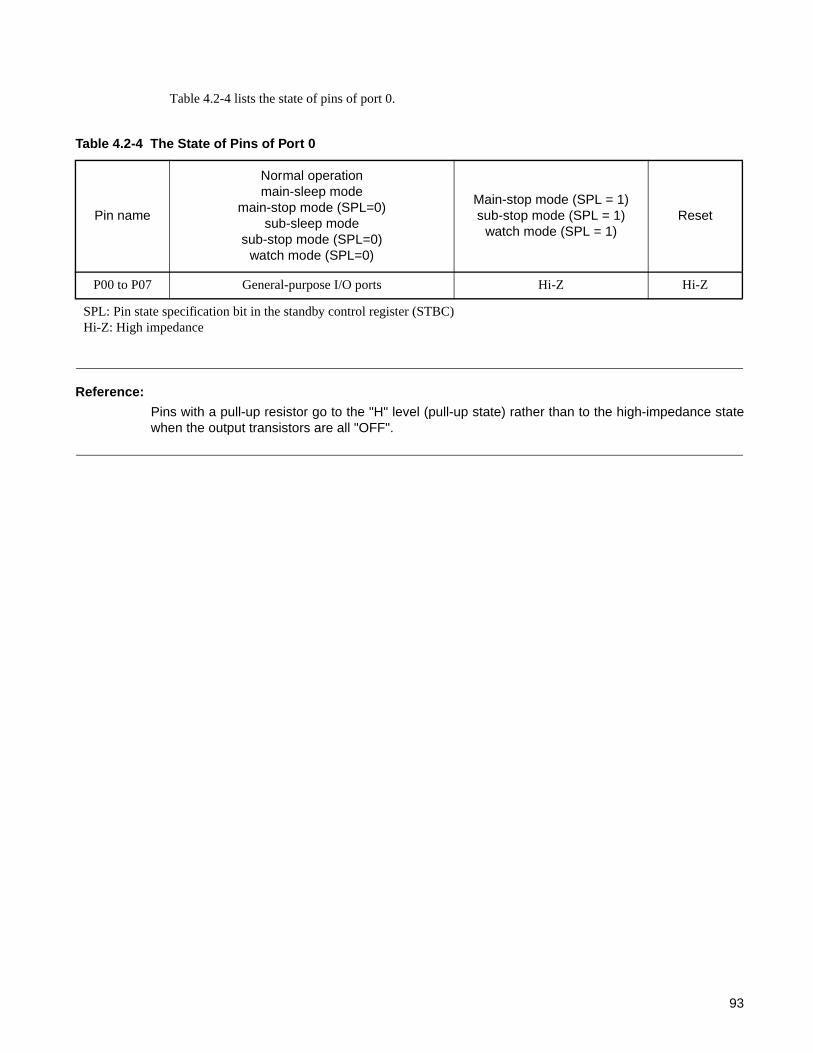
Table 4.2-4 lists the state of pins of port 0.
Reference:
Pins with a pull-up resistor go to the "H" level (pull-up state) rather than to the high-impedance statewhen the output transistors are all "OFF".
Table 4.2-4 The State of Pins of Port 0
Pin name
Normal operationmain-sleep mode
main-stop mode (SPL=0)sub-sleep mode
sub-stop mode (SPL=0)watch mode (SPL=0)
Main-stop mode (SPL = 1)sub-stop mode (SPL = 1)
watch mode (SPL = 1)Reset
P00 to P07 General-purpose I/O ports Hi-Z Hi-Z
SPL: Pin state specification bit in the standby control register (STBC)Hi-Z: High impedance
93
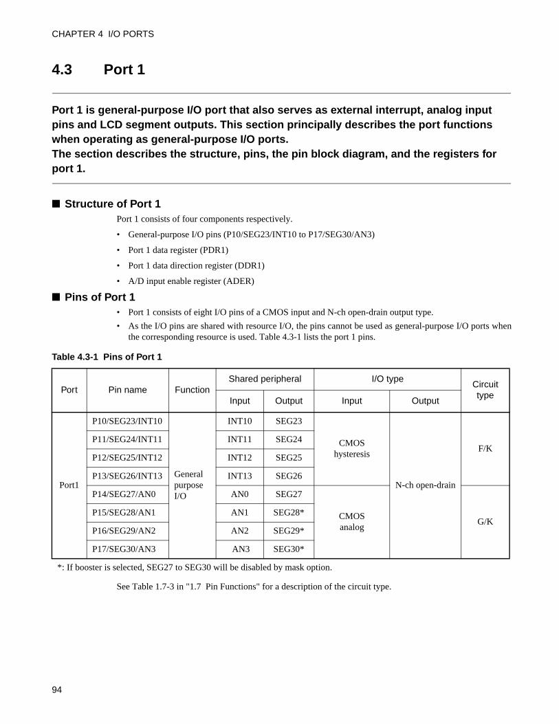
CHAPTER 4 I/O PORTS
4.3 Port 1
Port 1 is general-purpose I/O port that also serves as external interrupt, analog input pins and LCD segment outputs. This section principally describes the port functions when operating as general-purpose I/O ports.The section describes the structure, pins, the pin block diagram, and the registers for port 1.
Structure of Port 1Port 1 consists of four components respectively.
• General-purpose I/O pins (P10/SEG23/INT10 to P17/SEG30/AN3)
• Port 1 data register (PDR1)
• Port 1 data direction register (DDR1)
• A/D input enable register (ADER)
Pins of Port 1• Port 1 consists of eight I/O pins of a CMOS input and N-ch open-drain output type.
• As the I/O pins are shared with resource I/O, the pins cannot be used as general-purpose I/O ports whenthe corresponding resource is used. Table 4.3-1 lists the port 1 pins.
See Table 1.7-3 in "1.7 Pin Functions" for a description of the circuit type.
Table 4.3-1 Pins of Port 1
Port Pin name FunctionShared peripheral I/O type
Circuit type
Input Output Input Output
Port1
P10/SEG23/INT10
General purpose I/O
INT10 SEG23
CMOShysteresis
N-ch open-drain
F/KP11/SEG24/INT11 INT11 SEG24
P12/SEG25/INT12 INT12 SEG25
P13/SEG26/INT13 INT13 SEG26
P14/SEG27/AN0 AN0 SEG27
CMOSanalog
G/KP15/SEG28/AN1 AN1 SEG28*
P16/SEG29/AN2 AN2 SEG29*
P17/SEG30/AN3 AN3 SEG30*
*: If booster is selected, SEG27 to SEG30 will be disabled by mask option.
94

Block Diagram of Pins of Port 1
Figure 4.3-1 Block Diagram of Pins of Port 1
Port 1 Registers• The port 1 registers consist of PDR1, DDR1 and ADER.
• Each bit in these registers has a one-to-one relationship with port 1 pin respectively.
Table 4.3-2 shows the correspondence between pins and registers for port 1.
PDR (Port data register)
DDR
Inte
rnal
dat
a bu
s
PDR read
PDR read (for bit manipulation instructions)
PDR write
DDR write (Port direction register)
Pin
SPL: Pin state specification bit in the standby control register (STBC)
N-ch
Stop, watch mode (SPL = 1)
Output latch
External interrupt input enable
To external interrupt input
LCD output enable
Stop, watch mode
A/D converteranalog input
A/D converter channel selector
Mask Option
LCD segment output
A/D Input enable
Table 4.3-2 Correspondence between Pins and Registers for Port 1
Port Correspondence between register bits and pins
Port1
PDR1, DDR1 bit7 bit6 bit5 bit4 bit3 bit2 bit1 bit0
ADER bit7 bit6 bit5 bit4 - - - -
Corresponding pin P17 P16 P15 P14 P13 P12 P11 P10
95
CHAPTER 4 I/O PORTS
4.3.1 Port 1 Registers (PDR1, DDR1)
This section describes the port 1 registers.
Functions of Port 1 Register
Port 1 data register (PDR1)
The PDR1 register holds the pin states. Therefore, a bit corresponding to a pin set as an output port can be
read as the same state ("0" or "1") as the output latch, but when it is an input port, it cannot be read as the
output latch state.
Note:
For bit manipulation instructions (SETB and CLRB), since the state of output latch (not the pin) isread, the output latch states of bits other than those being operated on are not changed.
Port 1 data direction register (DDR1)
• The DDR1 register sets the direction (input or output) for each pin (bit).
• Setting "1" to the bit corresponding to a port (pin) sets the pin as an output port. Setting "0" sets the pinas an input port.
Note:
As the DDR1 register is write-only, the bit manipulation instructions (SETB and CLRB) cannot beused.
Settings when pins are used as external interrupt inputs
When port pins are used as external interrupt input pins, in addition to enabling the external interrupt circuit
(external interrupt 1), the corresponding pins must also be set as inputs. The corresponding output latch
data has no significance in this case.
Settings as an analog input
When port 1 pins are used as analog signal input pins, write "0" to the corresponding bits of DDR1 to set
the pin as input pin and write "1" to the corresponding bits of ADER to set the pin as analog input pin.
Settings as an LCD segment output
To use pins as LCD segment outputs, DDR1 corresponding bits for pins used for this purpose should be set
to turn the output transistor "OFF", to prevent it from interfering with the LCD segment output. Also set the
corresponding LCD output enable bit to the "enable" state.
96
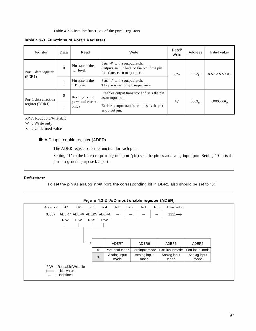
Table 4.3-3 lists the functions of the port 1 registers.
A/D input enable register (ADER)
The ADER register sets the function for each pin.
Setting "1" to the bit corresponding to a port (pin) sets the pin as an analog input port. Setting "0" sets the
pin as a general purpose I/O port.
Reference:
To set the pin as analog input port, the corresponding bit in DDR1 also should be set to "0".
Figure 4.3-2 A/D input enable register (ADER)
Table 4.3-3 Functions of Port 1 Registers
Register Data Read WriteRead/Write
Address Initial value
Port 1 data register (PDR1)
0Pin state is the "L" level.
Sets "0" to the output latch.Outputs an "L" level to the pin if the pin functions as an output port. R/W 0002H XXXXXXXXB
1Pin state is the "H" level.
Sets "1" to the output latch.The pin is set to high impedance.
Port 1 data direction register (DDR1)
0 Reading is not permitted (write-only)
Disables output transistor and sets the pin as an input pin.
W 0003H 00000000B
1Enables output transistor and sets the pin as output pin.
R/W: Readable/WritableW : Write onlyX : Undefined value
Address bit7 bit6 bit5 bit4 bit3 bit2 bit1 bit0 Initial value
0030H ADER7 ADER6 ADER5 ADER4 — — — — 1111----B
R/W R/W R/W R/W
ADER7 ADER6 ADER5 ADER4
0 Port input mode Port input mode Port input mode Port input mode
1Analog input
modeAnalog input
modeAnalog input
modeAnalog input
mode
R/W : Readable/Writable: Initial value
— : Undefined
97
CHAPTER 4 I/O PORTS
4.3.2 Operation of Port 1
This section describes the operations of the port 1.
Operation of Port 1
Operation as an output port
• Setting the corresponding DDR1 register bit to "1" sets a pin as an output port.
• When a pin is set as an output port, its output transistor is enabled and the pin outputs the data stored in
the output latch.
• Writing data to the PDR1 register stores the data in the output latch and outputs the data directly to the
pin. When the output latch value is "0", the output transistor turns "OFF" and an "L" level is output from
the pin. When the output latch value is "1", the output transistor turns "OFF" and the pin goes to high
impedance state.
• Reading the PDR1 register returns the pin value.
Operation as an input port
• Setting the corresponding DDR1 and ADER register bit to "0" sets a pin as an input port.
• When a pin is set as an input port, the output transistor is "OFF" and the pin goes to the high-impedance
state.
• Writing data to the PDR1 register store the data in the output latch of the PDR but does not output the
data to the pin.
• Reading the PDR1 register returns the pin value.
Operation as an external interrupt input
• When a port is an external interrupt input, the port is made an input by setting the corresponding DDR1
register bits to "0".
• Reading the PDR1 register returns the pin value, regardless of whether external interrupt inputs or
interrupt request outputs are enabled/disabled.
Operation as an analog input
• Set the DDR1 bit that corresponds to the analog input pin to "0" to turn the port to input port.
• Set the ADER corresponding bit to "1" to set the port as analog input port.
Operation as an LCD segment output
When the LCD output is selected, set the DDR1 register bits corresponding to the LCD segment output
pins to "0" to turn the output transistor "OFF".
98
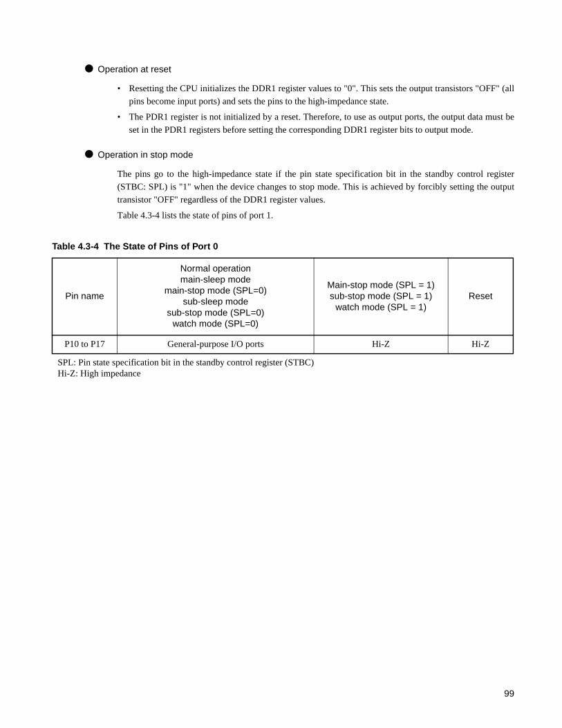
Operation at reset
• Resetting the CPU initializes the DDR1 register values to "0". This sets the output transistors "OFF" (all
pins become input ports) and sets the pins to the high-impedance state.
• The PDR1 register is not initialized by a reset. Therefore, to use as output ports, the output data must be
set in the PDR1 registers before setting the corresponding DDR1 register bits to output mode.
Operation in stop mode
The pins go to the high-impedance state if the pin state specification bit in the standby control register
(STBC: SPL) is "1" when the device changes to stop mode. This is achieved by forcibly setting the output
transistor "OFF" regardless of the DDR1 register values.
Table 4.3-4 lists the state of pins of port 1.
Table 4.3-4 The State of Pins of Port 0
Pin name
Normal operationmain-sleep mode
main-stop mode (SPL=0)sub-sleep mode
sub-stop mode (SPL=0)watch mode (SPL=0)
Main-stop mode (SPL = 1)sub-stop mode (SPL = 1)
watch mode (SPL = 1)Reset
P10 to P17 General-purpose I/O ports Hi-Z Hi-Z
SPL: Pin state specification bit in the standby control register (STBC)Hi-Z: High impedance
99
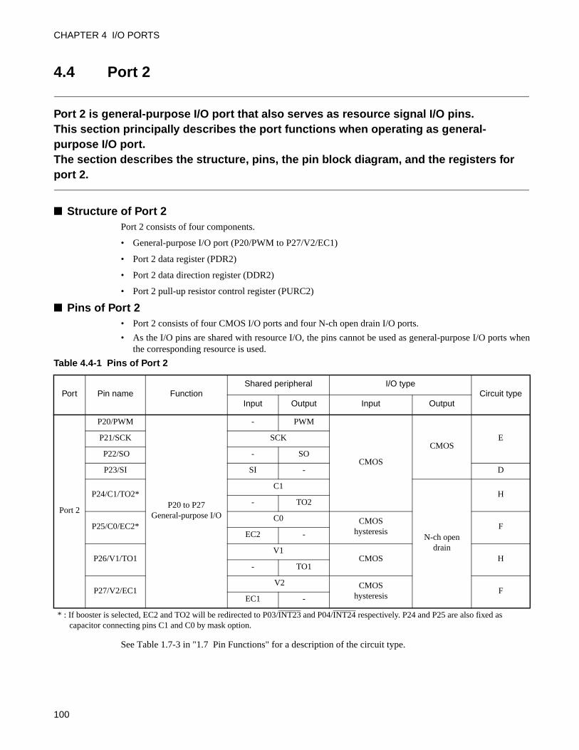
CHAPTER 4 I/O PORTS
4.4 Port 2
Port 2 is general-purpose I/O port that also serves as resource signal I/O pins.This section principally describes the port functions when operating as general-purpose I/O port.The section describes the structure, pins, the pin block diagram, and the registers for port 2.
Structure of Port 2Port 2 consists of four components.
• General-purpose I/O port (P20/PWM to P27/V2/EC1)
• Port 2 data register (PDR2)
• Port 2 data direction register (DDR2)
• Port 2 pull-up resistor control register (PURC2)
Pins of Port 2• Port 2 consists of four CMOS I/O ports and four N-ch open drain I/O ports.
• As the I/O pins are shared with resource I/O, the pins cannot be used as general-purpose I/O ports whenthe corresponding resource is used.
See Table 1.7-3 in "1.7 Pin Functions" for a description of the circuit type.
Table 4.4-1 Pins of Port 2
Port Pin name FunctionShared peripheral I/O type
Circuit typeInput Output Input Output
Port 2
P20/PWM
P20 to P27General-purpose I/O
- PWM
CMOS
CMOSEP21/SCK SCK
P22/SO - SO
P23/SI SI - D
P24/C1/TO2*C1
N-ch open drain
H- TO2
P25/C0/EC2*C0 CMOS
hysteresisF
EC2 -
P26/V1/TO1V1
CMOS H- TO1
P27/V2/EC1 V2 CMOS
hysteresisF
EC1 -
* : If booster is selected, EC2 and TO2 will be redirected to P03/INT23 and P04/INT24 respectively. P24 and P25 are also fixed as capacitor connecting pins C1 and C0 by mask option.
100

Block Diagram of Pins of Port 2
Figure 4.4-1 Block Diagram of Pins of Port 2 (P20 to P23)
Note:
When a port is used as a normal input port, peripheral circuit operation that uses the same pins mustbe disabled.
PDR (Port data register)
DDR
Inte
rna
l da
ta b
us
PDR read
PDR read (for bit manipulation instructions)
Output latch
PDR write
DDR write
Pin
SPL: Pin state specification bit in the standby control register (STBC)
N-ch
Stop, watch mode
To peripheral input
Stop, watch mode
P-ch
DDR read
Pull-up resistor
P-ch
Approx. 50kΩ
(Port direction register)
Pull-up resistor control register
(SPL = 1)
Peripheral output
Peripheral output
enable
101

CHAPTER 4 I/O PORTS
Figure 4.4-2 Block Diagram of Pins of Port 2 (P24, P25)
Note:
When a port is used as a normal input port, peripheral circuit operation that uses the same pins mustbe disabled.
PDR (Port data register)
DDR
Inte
rnal
dat
a bu
s
PDR read
PDR read (for bit manipulation instructions)
Output latch
PDR write
DDR write
Pin
* : If booster is selected by mask option, C0, C1 will connect to pin by mask option and input buffer will be disabled to avoid current leakage.
SPL: Pin state specification bit in the standby control register (STBC)
N-ch
Stop, watch mode
To peripheral input
(Port direction register)
DDR read
Stop, watch mode
Maskoption *
(SPL = 1)
Peripheral output
Peripheral output enable
Booster
Maskoption *
102
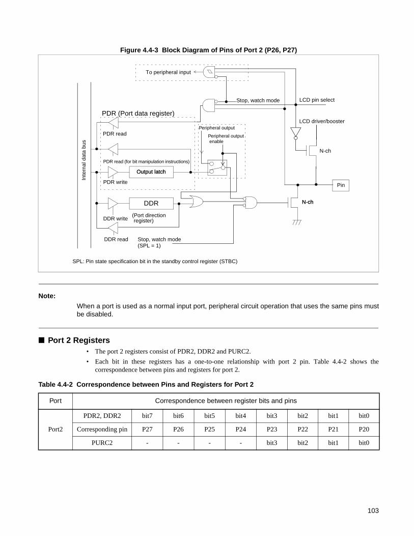
Figure 4.4-3 Block Diagram of Pins of Port 2 (P26, P27)
Note:
When a port is used as a normal input port, peripheral circuit operation that uses the same pins mustbe disabled.
Port 2 Registers• The port 2 registers consist of PDR2, DDR2 and PURC2.
• Each bit in these registers has a one-to-one relationship with port 2 pin. Table 4.4-2 shows thecorrespondence between pins and registers for port 2.
PDR (Port data register)
DDR
Inte
rnal
dat
a bu
s
PDR read
PDR read (for bit manipulation instructions)
Output latch
PDR write
DDR write
Pin
SPL: Pin state specification bit in the standby control register (STBC)
N-ch
Stop, watch mode
To peripheral input
(Port direction register)
DDR read
Stop, watch mode
(SPL = 1)
Peripheral output
Peripheral output enable
LCD driver/booster
LCD pin select
N-ch
N-ch
Output latch
Table 4.4-2 Correspondence between Pins and Registers for Port 2
Port Correspondence between register bits and pins
Port2
PDR2, DDR2 bit7 bit6 bit5 bit4 bit3 bit2 bit1 bit0
Corresponding pin P27 P26 P25 P24 P23 P22 P21 P20
PURC2 - - - - bit3 bit2 bit1 bit0
103
CHAPTER 4 I/O PORTS
4.4.1 Port 2 Registers (PDR2, DDR2, PURC2)
This section describes the port 2 registers.
Functions of Port 2 Register
Port 2 data register (PDR2)
The PDR2 register holds the pin states. Therefore, a bit corresponding to a pin set as an output port can be
read as the same state ("0" or "1") as the output latch, but when it is an input port, it cannot be read as the
output latch state.
Note:
For bit manipulation instructions (SETB and CLRB), since the state of output latch (not the pin) isread, the output latch states of bits other than those being operated on are not changed.
Port 2 data direction register (DDR2)
• The DDR2 register sets the direction (input or output) for each pin (bit).
• Setting "1" to the bit corresponding to a port (pin) sets the pin as an output port. Setting "0" sets the pinas an input port.
Settings as peripheral output
To use a peripheral that has an output pin, set the peripheral output enable bit for that pin to the "enable"
state. As can be seen in the block diagram, the peripheral has precedence over the general-purpose port for
use of the output pin. Once the peripheral output is enabled, the states set in the PDR2 and DDR2 registers
are no longer valid, and do not affect the data output by the peripheral, or the enabling of the output.
Settings as a peripheral input
To use a peripheral that has a port 2 pin as an input pin, set that pin as an input port. The output latch data
for that pin will no longer be valid.
Setting as LCD driver / booster pin
To use pins as LCD driver/booster pin, DDR2 corresponding bits for pins used for this purpose should be
set to turn the output transistor "OFF", to prevent it from interfering with the LCD driver/booster operation.
Also set the corresponding LCD pin select bit to the "enable" state.
Note:
As the peripheral has precedence over the DDR2 setting, do not enable the peripheral when the pinis used for LCD driver/booster.
104

Table 4.4-3 shows the function of the register of port 2.
Port 2 pull-up resistor control register (PURC2)
By using pull-up resistor control register (PURC2), it is possible to turn on/off pull-up resistor.
When pull-up resistor is selected in pull-up resistor control register, the states of these pins in stop mode
(SPL=1) are in "H" level (pull-up state) rather than high impedance. However, during reset, pull-up is
unavailable and will be in high impedance state. Figure 4.4-4 shows the setting of port 2 pull-up resistor
control register.
Figure 4.4-4 Pull-up resistor control register setting (PURC2)
Table 4.4-3 Functions of Port 2 Register
Register Data Read Write Read/Write Address Initial value
Port 2 data register (PDR2)
0Pin state is the "L" level.
Sets "0" to the output latch.Outputs an "L" level to the pin if the pin functions as an output port.
R/W 0004H 00000000B
1Pin state is the "H" level.
Sets "1" to the output latch.Outputs an "H" level to the pin if the pin functions as an output port for P20 to P23. The pin is set to high impedance for P24 to P27.
Port 2 data direction register (DDR2)
0 Input portDisables output transistor and sets the pin as an input pin.
R/W 0006H 00000000B
1 output portEnables output transistor and sets the pin as output pin.
R/W: Readable/Writable
PURC2
Address bit7 bit6 bit5 bit4 bit3 bit2 bit1 bit0 Initial value
0072H — — — — PUR23 PUR22 PUR21 PUR20 ----1111B
R/W R/W R/W R/W
PUR23 PUR22 PUR21 PUR20
0 P23 pull up ON P22 pull up ON P21 pull up ON P20 pull up ON
1 P23 pull up OFF P22 pull up OFF P21 pull up OFF P20 pull up OFF
R/W : Readable/Writable: Initial value
— : Undefined
105
CHAPTER 4 I/O PORTS
4.4.2 Operation of Port 2
This section describes the operations of the port 2.
Operation of Port 2
Operation as an output port
• Setting the corresponding DDR2 register bit to "1" sets a pin as an output port.
• When a pin is set as an output port, its output transistor is enabled and the pin outputs the data stored in
the output latch.
• Writing data to the PDR2 register stores the data in the output latch of the PDR and outputs the data
directly to the pin.
• Reading the PDR2 register returns the pin value. P26, P27 are default to function as LCD power pins.
When P26, P27 are set to function as general purpose I/O ports (by setting LCR2:PSEL to "1") reading
PDR2:bit6 and PDR2:bit7 return the corresponding pin values.
Operation as an input port
• Setting the corresponding DDR2 register bit to "0" set P20 to P25 as an input port.
• Setting the corresponding DDR2 register bit to "0" and LCR2 :PSEL to "1" set P26, P27 as an input
port.
• When a pin is set as an input port, the output transistor is "OFF" and the pin goes to the high-impedance
state.
• Writing data to the PDR2 registers stores the data in the output latch but does not output the data to the
pin.
• Reading the PDR2 register returns the pin values.
Reference:
If booster is selected by mask option, bit 4 and bit 5 of PDR2 are always read as "0" for pin P24 andP25.
Operation as a peripheral output
• If a peripheral output enable bit is set to "enable", the corresponding pin becomes a peripheral output.
• Reading the PDR2 register returns the pin value, regardless of whether peripheral output is enabled/
disabled.
Operation as a peripheral input
• A port pin is set as a peripheral input by setting the corresponding DDR2 register bit to "0".
• Reading the PDR2 register returns the pin value, regardless of whether or not the peripheral input is
used.
106

Operation as LCD driver/booster pin
• When the LCD driver/booster is selected, set the DDR2 register bits corresponding to the LCD driver/
booster pins to "0" to turn the output transistor "OFF".
• Setting LCR2 :PSEL to "0" will set the P26 and P27 as LCD power supply pin V1 and V2. If booster is
selected by mask option, C0 and C1 will connect to P25 and P24, EC2 and TO2 will be redirected to
P03 and P04 respectively.
Operation at reset
Resetting the CPU initializes both the PDR2 and DDR2 register values to "0". This sets the output
transistor "OFF" (all pins become input ports) and sets the pins to the high-impedance state.
Operation in stop mode
The pins go to the high-impedance state if the pin state specification bit in the standby control register
(STBC:SPL) is "1" when the device changes to stop mode. This is achieved by forcibly setting the output
transistor "OFF" regardless of the DDR2 register values.
Table 4.4.4 lists the port 2 pin states.
Reference:
Pins with a pull-up resistor go to the "H" level (pull-up state) rather than the high-impedance statewhen the output transistors are all "OFF".
Table 4.4-4 Port 2 Pin state
Pin name
Normal operationmain-sleep mode
main-stop mode (SPL=0)sub-stop mode
sub-stop mode (SPL=0)watch mode (SPL=0)
Main-stop mode (SPL=1)sub-stop mode (SPL=1)
watch mode (SPL=1)Reset
P20/PWM, P21/SCK,P22/SO, P23/SI
General-purpose I/O ports/peripheral I/O Hi-Z
Hi-Z
P24/C1/TO2 Hi-Z/C1 *
P25/C0/EC2 Hi-Z/C0 *
P26/V1/TO1 V1
P27/V2/EC1 V2
* : When booster is selectedSPL: Pin state specification bit in the standby control register (STBC)Hi-Z: High impedance
107

CHAPTER 4 I/O PORTS
4.5 Port 3
Port 3 is a general-purpose output only port that also serves as the LCD common outputs. This section principally describes the port functions when operating as a general-purpose output port.The section describes the structure, pins, the pin block diagram, and the port registers for port 3.
Structure of Port 3Port 3 consists of the following two components:
• General-purpose output port/LCD common output pins (P30/COM2, P31/COM3)
• Port 3 data register (PDR3)
Pins of Port 3Port 3 consists of two N-channel open-drain pins output. P30 and P31 are also used as LCD common
output pins COM2 and COM3. While it is being used by LCD, this pin cannot be used as the general-
purpose output port. Table 4.5-1 lists the port 3 pins.
See Table 1.7-3 in "1.7 Pin Functions" for a description of the circuit type.
Table 4.5-1 Pins of Port 3
Port Pin name FunctionShared peripheral I/O type
Circuit typeOutput Input Output
Port 3P30/COM2
General-purpose I/OCOM2
— N-ch open-drain I/KP31/COM3 COM3
108
Block Diagram of Pins of Port 3
Figure 4.5-1 Block Diagram of Pins of Port 3
Port 3 Register• The port 3 register consists of PDR3.
• Each bit in the register has a one-to-one relationship with port 3 pin.
Table 4.5-2 shows the correspondence between pins and register for port 3.
PDR (Port data register)
Inte
rnal
dat
a bu
s
PDR read
Output latch
PDR writePin
SPL: Pin state specification bit in the standby control register (STBC)
N-chStop, watch mode (SPL = 1)
LCD common output
LCD output enable
N-ch
Table 4.5-2 Correspondence between Pins and Registers for Port 3
Port Correspondence between register bits and pins
Port3PDR3 bit7 bit6 bit5 bit4 bit3 bit2 bit1 bit0
Corresponding pin - - - - - - P31 P30
109

CHAPTER 4 I/O PORTS
4.5.1 Port 3 Register (PDR3)
This section describes the port 3 register.
Functions of Port 3 Register
Port 3 data register (PDR3)
The PDR3 register holds the output latch states. Therefore, it does not read out as the pin.
Settings as an LCD common output
To use pins as LCD common outputs, PDR3 corresponding bits for pins used for this purpose should be set
to turn the output transistor "OFF", to prevent it from interfering with the LCD common output. Also set
the corresponding LCD output enable bit to the "enable" state.
Table 4.5-3 lists the functions of the port 3 registers.
Table 4.5-3 Functions of Port 3 Register
Register Data Read Write Read/Write Address Initial value
Port 3 data register (PDR3)
0Output latch value is "0"
Sets "0" to the output latch.Outputs an "L" level to the pin.
R/W 000CH ------11B
1Output latch value is "1"
Sets "1" to the output latch.The pin is set to high impedance.
R/W: Readable/Writable
110

4.5.2 Operation of Port 3
This section describes the operations of the port 3.
Operation of Port 3
Operation as an output port
• Writing data to the PDR3 register stores the data in the output latch. When the output latch value is "0",
the output transistor turns "ON" and an "L" level is output from the pin. When the output latch value is
"1", the transistor turns "OFF" and the pin goes to the high-impedance state.
• Reading the PDR3 register returns output latch value.
Operation as an LCD common output
• When the LCD output is selected, set the PDR3 register bits corresponding to the LCD common output
pins to "1" to turn the output transistor "OFF".
• You cannot read the LCD output data by reading PDR3 register. (If you read the PDR registers, you will
get the output latch data, not the LCD output data.)
Operation at reset
Resetting the CPU initializes the PDR3 register value to "1". This sets output transistors "OFF" and sets the
pins to the high-impedance state.
Operation in stop mode
The pins go to the high-impedance state, if the pin state specification bit in the standby control register
(STBC: SPL) is "1" when the device changes to stop mode. This is achieved by forcibly setting the output
transistor "OFF" regardless of the PDR3 register value.
Table 4.5-4 lists the port 3 pin states.
Table 4.5-4 Port 3 Pin State
Pin name
Normal operationmain-sleep mode
main-stop mode (SPL=0)sub-sleep mode
sub-stop mode (SPL=0)watch mode (SPL=0)
Main-stop mode (SPL = 1)sub-stop mode (SPL = 1)
watch mode (SPL = 1)Reset
P30/COM2, P31/COM3General-purpose output port/LCD common output
Hi-Z Hi-Z
SPL: Pin state specification bit in the standby control register (STBC)Hi-Z: High impedance
111

CHAPTER 4 I/O PORTS
4.6 Port 4
Port 4 is general-purpose I/O port that also serves as LCD segment output. This section principally describes the port functions when operating as general-purpose output ports. The section describes the structure, pins, the pin block diagram, and the registers for port 4.
Structure of Port 4 Port 4 consists of two components.
• General-purpose I/O pins/LCD segment output pins (P40/SEG8 to P47/SEG15)
• Port 4 data register (PDR4)
Pins of Port 4Port 4 consists of eight N-channel open-drain I/O ports.
When P40 to P47 are used as LCD segment output pins, they cannot be used as general purpose I/O pins.
Table 4.6-1 lists the port 4 pins.
Table 4.6-1 Pins of Port 4
Port Pin name FunctionShared peripheral I/O type
Circuit typeOutput Input Output
Port 4
P40/SEG8
P40 to P47General purpose I/O
SEG8
CMOSN-ch open
drainH/K
P41/SEG9 SEG9
P42/SEG10 SEG10
P43/SEG11 SEG11
P44/SEG12 SEG12
P45/SEG13 SEG13
P46/SEG14 SEG14
P47/SEG15 SEG15
See Table 1.7-3 in "1.7 Pin Functions" for a description of the circuit type.
112
Block Diagram of Pins of Port 4
Figure 4.6-1 Block Diagram of Pins of Port 4
Note:
Do not use the pins as output ports if using as an LCD segment output.
Port 4 Register• The port 4 register consists of PDR4.
• Each bit in the register has a one-to-one relationship with port 4.
Table 4.6-2 shows the correspondence between pins and register for port 4.
PDR (Port data register)
Inte
rnal
dat
a bu
s
PDR read
PDR read (for bit manipulation instructions)
Output latch
PDR writePin
SPL: Pin state specification bit in the standby control register (STBC)
N-chStop, watch mode (SPL = 1)
LCD segment output
Stop,
LCD output enable
watch mode
N-ch
Table 4.6-2 Correspondence between Pins and Registers for Port 4
Port Correspondence between register bits and pins
Port4PDR4 bit7 bit6 bit5 bit4 bit3 bit2 bit1 bit0
Corresponding pin P47 P46 P45 P44 P43 P42 P41 P40
113

CHAPTER 4 I/O PORTS
4.6.1 Port 4 Registers (PDR4)
This section describes the port 4 register.
Functions of Port 4 Register
Port 4 data register (PDR4)
The PDR4 register holds the pin states. Therefore, a bit corresponding to a pin set as an output port can be
read as the same state ("0" or "1") as the output latch, but when it is an input port, it cannot be read as the
output latch state.
Note:
For bit manipulation instructions (SETB and CLRB), since the state of output latch (not the pin) isread, the output latch states of bits other than those being operated on are not changed.
Settings as an LCD segment output
To use pins as LCD segment outputs, PDR4 corresponding bits for pins used for this purpose should be set
to turn the output transistor "OFF", to prevent it from interfering with the LCD segment output. Also set the
corresponding LCD output enable bit to the "enable" state.
Table 4.6-3 lists the functions of the port 4 register.
Table 4.6-3 Functions of Port 4 Register
Register Data Read Write Read/Write Address Initial value
Port 4 data register (PDR4)
0Output latch pin state is the "L" level.
Sets "0" to the output latch.Outputs an "L" level to the pin.
R/W 0010H 11111111B
1Output latch pin state is the "H" level.
Sets "1" to the output latch.The pin is set to high impedance.
R/W: Readable/Writable
114

4.6.2 Operation of Port 4
This section describes the operations of the port 4.
Operation of Port 4
Operation as an output port
• Writing data to the PDR4 register stores the data in the output latch. When the output latch value is "0",
the output transistor turns "ON" and an "L" level is output from the pin. When the output latch value is
"1", the transistor turns "OFF" and the pin goes to the high-impedance state.
• Reading the PDR4 register returns output latch value.
Operation as an input port
• To set the pin as an input port, write "1" to the bits in the PDR4 register. The output transistor is "OFF".
• Reading the PDR4 register returns the pin value.
Operation as LCD segment output
• When the LCD output is selected, set the PDR4 register bits corresponding to the LCD segment output
pins to "1" to turn the output transistor "OFF".
• You cannot read the LCD output data by reading PDR4 register.
Operation at reset
Resetting the CPU initializes the PDR4 register values to "1". This turns all the output transistors "OFF"
and sets the pins to the high-impedance state.
Operation in stop mode
The output transistors are forcibly turned "OFF" and the pins go to the high-impedance state if the pin state
specification bit in the standby control register (STBC:SPL) is "1" when the device changes to stop mode.
Table 4.6-4 lists the port 4 pin states.
Table 4.6-4 Port 4 Pin State
Pin name
Normal operationmain-sleep mode
main-stop mode (SPL=0)sub-sleep mode
sub-stop mode (SPL=0)watch mode (SPL=0)
Main-stop mode (SPL = 1)sub-stop mode (SPL = 1)
watch mode (SPL = 1)Reset
P40/SEG8 to P47/SEG15General-purpose output port/LCD segment output
Hi-Z Hi-Z
SPL: Pin state specification bit in the standby control register (STBC)Hi-Z: High impedance
115

CHAPTER 4 I/O PORTS
4.7 Port 5
Port 5 is general-purpose I/O port that also serves as LCD segment output. This section principally describes the port functions when operating as general-purpose output ports. The section describes the structure, pins, the pin block diagram, and the registers for port 5.
Structure of Port 5Port 5 consists of two components.
• General-purpose I/O pins/LCD segment output pins (P50/SEG16 to P56/SEG22), general-purpose input
only pin P57
• Port 5 data register (PDR5)
Pins of Port 5Port 5 consists of seven I/O pins of N-ch open-drain type and one input only port. lists the port 5 pins.
See Table 1.7-3 in "1.7 Pin Functions" for a description of the circuit type.
Table 4.7-1 Pins of Port 5
Port Pin name Function
Shared peripheral
I/O typeCircuit type
Output Input Output
Port 5
P50/SEG16
P50 to P56General-purpose I/O
SEG16
CMOSNch open-
drainH/K
P51/SEG17 SEG17
P52/SEG18 SEG18
P53/SEG19 SEG19
P54/SEG20 SEG20
P55/SEG21 SEG21
P56/SEG22 SEG22
P57P57
General-purpose input— CMOS — J
116

Block Diagram of Pins of Port 5
Figure 4.7-1 Block Diagram of Pins of Port 5 (P50 to P56)
Figure 4.7-2 Block Diagram of Pins of Port 5 (P57)
Port 5 Register• The port 5 register consists of PDR5.
• Each bit in the register has a one-to-one relationship with port 5.
Table 4.7-1 lists the correspondence between pins and register for port 5.
PDR (Port data register)
Inte
rnal
dat
a bu
s
PDR read
PDR read (for bit manipulation instructions)
Output latch
PDR write
SPL: Pin state specification bit in the standby control register (STBC)
Stop, watch mode (SPL = 1)
LCD output enable
Pin
N-ch
LCD segment output
Stop, watch mode
N-ch
PDR (Port data register)
Inte
rnal
dat
a bu
s
PDR read
Pin
P57
Table 4.7-2 Correspondence between Pins and Registers for Port 5
Port Correspondence between register bits and pins
Port5PDR5 bit7 bit6 bit5 bit4 bit3 bit2 bit1 bit0
Corresponding pin P57 P56 P55 P54 P53 P52 P51 P50
117

CHAPTER 4 I/O PORTS
4.7.1 Port 5 Register (PDR5)
This section describes the port 5 register.
Functions of Port 5 Register
Port 5 data register (PDR5)
The PDR5 register holds the pin states. Therefore, a bit corresponding to a pin set as an output port can be
read as the same state ("0" or "1") as the output latch, but when it is an input port, it cannot be read as the
output latch state.
Note:
For bit manipulation instructions (SETB and CLRB), since the state of output latch (not the pin) isread, the output latch states of bits other than those being operated on are not changed.
Settings as an LCD segment output
To use pins as LCD segment outputs, PDR5 corresponding bits for pins used for this purpose should be set
to turn the output transistor "OFF", to prevent it from interfering with the LCD segment output. Also set the
corresponding LCD output enable bit to the "enable" state.
Table 4.7-3 lists the functions of the port 5 register.
Table 4.7-3 Functions of Port 5 Register
Register Data Read WriteRead/Write
Address Initial value
Port 5 data register (PDR5)
0Pin state is the "L" level.
Sets "0" to the output latch.Outputs "L" level to the pin if the pin functions as an output port.(no effect for P57) R/W 0012H X1111111B
1Pin state is the "H" level.
Sets "1" to the output latch.The pin is set to high impedance.(no effect for P57)
R/W: Readable/WritableX: Undefined value
118
4.7.2 Operation of Port 5
This section describes the operations of the port 5.
Operation of Port 5
Operation as an output port
• Writing data to the PDR5 register stores the data in the output latch. When the output latch value is "0",the output transistor turns "ON" and an "L" level is output from the pin. When the output latch value is"1", the transistor turns "OFF" and the pin goes to the high-impedance state. (P57 is an input only port,writing "0" to PDR5:bit7 has no effect for P57)
• Reading the PDR5 register returns output latch value.
Operation as an input port
• To set the pin as an input port, write "1" to the bits in the PDR5 register. The output transistor is "OFF".(P57 is an input only port, writing "1" to PDR5:bit7 has no effect for P57)
• Reading the PDR5 register returns the pin value.
Operation as LCD segment output
• When the LCD output is selected, set the PDR5 register bits corresponding to the LCD segment outputpins to "1" to turn the output transistor "OFF".
• You cannot read the LCD output data by reading PDR5 register.
Operation at reset
Resetting the CPU initializes the PDR5 register values to "1". This turns all the output transistors "OFF"
and sets the pins to the high-impedance state.
Operation in stop mode
The output transistors are forcibly turned "OFF" and the pins go to the high-impedance state if the pin state
specification bit in the standby control register (STBC:SPL) is "1" when the device changes to stop mode.
Table 4.7-4 lists the port 5 pin states.
Table 4.7-4 Port 5 Pin State
Pin name
Normal operationmain-sleep mode
main-stop mode (SPL=0)sub-sleep mode
sub-stop mode (SPL=0)watch mode (SPL=0)
Main-stop mode (SPL = 1)sub-stop mode (SPL = 1)
watch mode (SPL = 1)Reset
P50 to P56 General-purpose I/O portsHi-Z Hi-Z
P57 General-purpose input ports
SPL: Pin state specification bit in the standby control register (STBC)Hi-Z: High impedance
119
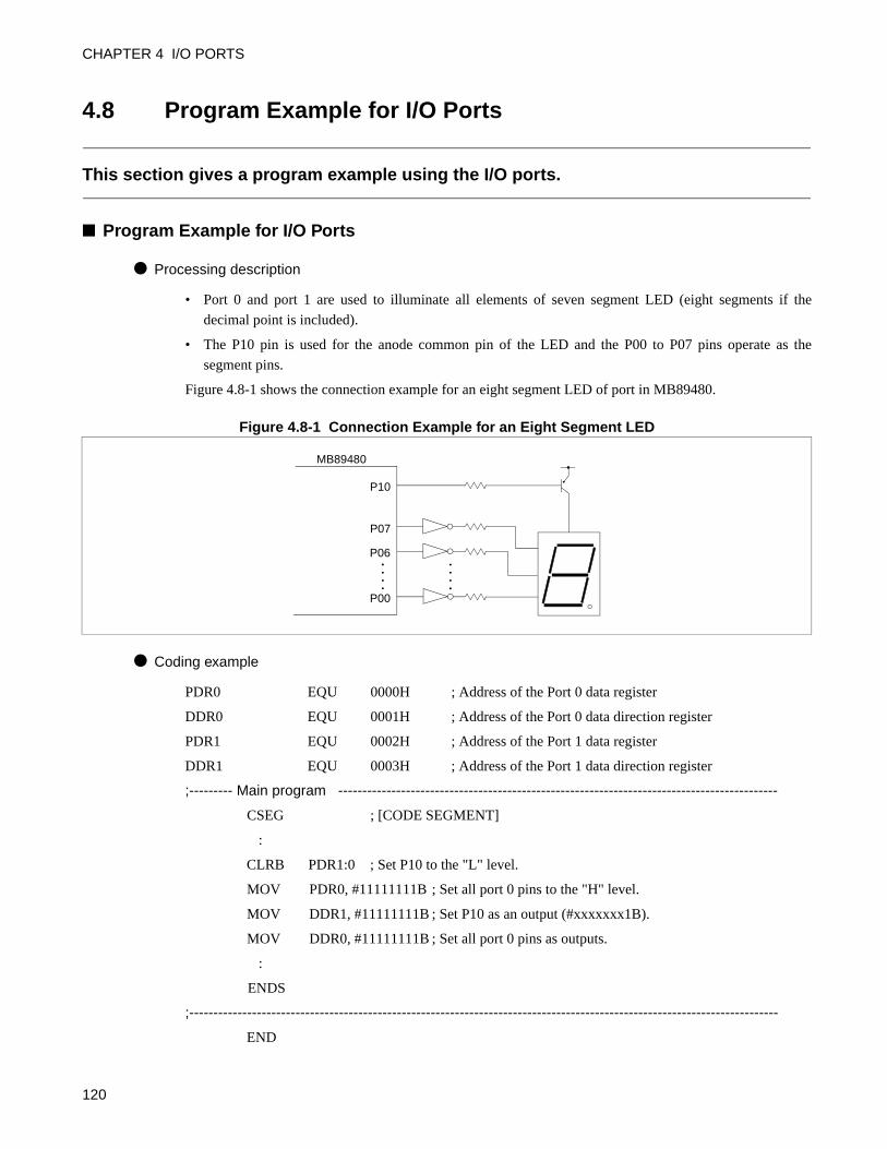
CHAPTER 4 I/O PORTS
4.8 Program Example for I/O Ports
This section gives a program example using the I/O ports.
Program Example for I/O Ports
Processing description
• Port 0 and port 1 are used to illuminate all elements of seven segment LED (eight segments if the
decimal point is included).
• The P10 pin is used for the anode common pin of the LED and the P00 to P07 pins operate as the
segment pins.
Figure 4.8-1 shows the connection example for an eight segment LED of port in MB89480.
Figure 4.8-1 Connection Example for an Eight Segment LED
Coding example
PDR0 EQU 0000H ; Address of the Port 0 data register
DDR0 EQU 0001H ; Address of the Port 0 data direction register
PDR1 EQU 0002H ; Address of the Port 1 data register
DDR1 EQU 0003H ; Address of the Port 1 data direction register
;--------- Main program -------------------------------------------------------------------------------------------
CSEG ; [CODE SEGMENT]
:
CLRB PDR1:0 ; Set P10 to the "L" level.
MOV PDR0, #11111111B ; Set all port 0 pins to the "H" level.
MOV DDR1, #11111111B ; Set P10 as an output (#xxxxxxx1B).
MOV DDR0, #11111111B ; Set all port 0 pins as outputs.
:
ENDS
;--------------------------------------------------------------------------------------------------------------------------
END
. . . .
. . . .
P00
P06
P07
P10
MB89480
120
CHAPTER 5TIME-BASE TIMER
This chapter describes the functions and operation of the time-base timer.
5.1 Overview of Time-base Timer
5.2 Block Diagram of Time-base Timer
5.3 Time-base Timer Control Register (TBTC)
5.4 Time-base Timer Interrupt
5.5 Operation of Time-base Timer
5.6 Notes on Using Time-base Timer
5.7 Program Example for Time-base Timer
121

CHAPTER 5 TIME-BASE TIMER
5.1 Overview of Time-base Timer
The time-base timer provides interval timer functions. Four different interval times can be selected. The time-base timer uses a 21-bit free-run counter which counts-up in sync with the internal count clock (divide-by-two the main clock source oscillation). The time-base timer also provides the timer output for the main clock oscillation stabilization wait time and the operating clock for the peripheral functions such as the watchdog timer and buzzer, continuous activation clock for the A/D converter.The time-base timer stops operating in modes in which the main clock source oscillation is stopped.
Interval Timer FunctionThe interval timer function generates repeated interrupt requests at fixed time intervals.
• The timer generates an interrupt request each time the interval timer bit overflows on the time-base
timer counter.
• The interval time can be selected from four different settings.
Table 5.1-1 lists the available interval time for the time-base timer.
Table 5.1-1 Time-base timer Interval time
Internal count clock cycle Interval time
2/FCH (0.16 µs)
213/FCH (approx. 0.66 ms)
215/FCH (approx. 2.62 ms)
218/FCH (approx. 21.0 ms)
222/FCH (approx. 335.5 ms)
FCH: Main clock source oscillationThe values enclosed in parentheses are for a 12.5 MHz main clock source oscillation.
122

Clock Supply FunctionThe clock supply function provides the timer output used for the main clock oscillation stabilization wait
time (three values), and operation clock for some peripheral functions. Table 5.1-2 lists the cycles of the
clocks that the time-base timer supplies to various peripheral functions.
Note:
The oscillation stabilization wait time should be used as a guide line since the oscillation cycle isunstable immediately after oscillation starts.
Table 5.1-2 Cycles of Clocks Supplied by Time-base Timer
Clock destination Clock cycle Remarks
Main clock oscillation stabilization wait time
214/FCH (approx. 1.31 ms)Selected by the oscillation stabilization wait time select bits of the system clock control register (SYCC: WT1, WT0), which is in the clock control section.
217/FCH (approx. 10.5 ms)
218/FCH (approx. 21.0 ms)
Watchdog timer 221/FCH (approx. 167.8 ms) Count-up clock for the watchdog timer
Buzzer output 29/FCH to 212/FCH (approx. 41.0 to 327.7 µs) See "CHAPTER 16 BUZZER OUTPUT".
A/D converter 28/FCH (approx. 20.5 µs) Clock for continuous activation
LCD controller/driver 27/FCH (approx. 10.2 µs) Frame cycle clock
FCH: Main clock source oscillationThe values enclosed in parentheses are for a 12.5 MHz main clock source oscillation.
123
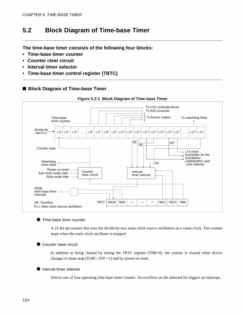
CHAPTER 5 TIME-BASE TIMER
5.2 Block Diagram of Time-base Timer
The time-base timer consists of the following four blocks:• Time-base timer counter• Counter clear circuit• Interval timer selector• Time-base timer control register (TBTC)
Block Diagram of Time-base Timer
Figure 5.2-1 Block Diagram of Time-base Timer
Time-base timer counter
A 21-bit up-counter that uses the divide-by-two main clock source oscillation as a count clock. The counter
stops when the main clock oscillator is stopped.
Counter clear circuit
In addition to being cleared by setting the TBTC register (TBR=0), the counter is cleared when device
changes to main stop (STBC: STP =1) and by power-on reset.
Interval timer selector
Selects one of four operating time-base timer counter. An overflow on the selected bit triggers an interrupt.
TBOF TBIE — — — TBC1 TBC0 TBRTBTC
OFOF
OF
⎞⎟⎠
Time-base timer counter
Divide-by-two FCH
Watchdog timer clear
Power-on reset
Stop mode start
IRQB time-base timer interrupt
OF: Overflow FCH: Main clock source oscillation
Counter clear circuit
To A/D converter
Interval timer selector
To watchdog timer
To clock controller for the oscillation stabilization wait time selector
× 21 × 22 × 23 . . . × 26 × 27 × 28 × 29 × 210 × 211 × 212 × 213 × 214 × 215 × 216 × 217 . . . × 220 × 221
To buzzer output
⎞⎟⎠
OF
Sub clock mode start
Counter clear
To LCD controller/driver
124

Time-base Timer Control Register (TBTC)
The TBTC register is used to select the interval time, clear the counter, control interrupt requests, and
check the state of the time-base timer.
125

CHAPTER 5 TIME-BASE TIMER
5.3 Time-base Timer Control Register (TBTC)
The time-base timer control register (TBTC) is used to select the interval times bit, clear the counter, control interrupts, and check the state of the time-base timer.
Time-base Timer Control Register (TBTC)
Figure 5.3-1 Time-base Timer Control Register (TBTC)
Address bit7 bit6 bit5 bit4 bit3 bit2 bit1 bit0 Initial value
000AH TBOF TBIE — — — TBC1 TBC0 TBR 00---000B
R/W R/W R/W R/W W
TBRTime-base timer initialization bit
Read Write
0 —Clears time-base timer
counter
1Reading always returns
"1".No effect. The bit does
not change.
TBC1 TBC0 Interval time selection bits
0 0 213/FCH
0 1 215/FCH
1 0 218/FCH
1 1 222/FCH
FCH: Main clock source oscillation
TBIE Interrupt request enable bit
0 Disables interrupt request output.
1 Enables interrupt request output.
TBOFOverflow interrupt request flag bit
Read Write
0No overflow on specified
bitClears this bit.
1 Overflow on specified bitNo effect. The bit does
not change.R/W :Readable/WritableW : Write only— : Undefined
: Initial value
126

Table 5.3-1 Functions of Time-base Timer Control Register (TBTC)
Bit name Function
bit7TBOF: Overflow interrupt request flag bit
This bit is set to "1" when counter overflow occurs on the specified bit of the time-base timer counter.An interrupt request is output when both this bit and the interrupt request enable bit (TBIE) are "1".Writing "0" clears this bit. Writing "1" has no effect and does not change the bit value.
bit6TBIE: interrupt request enable bit
This bit enables or disables an interrupt request output to the CPU. An interrupt request is output when both this bit and the overflow interrupt request flag bit (TBOF) are "1".
bit5to
bit3Undefined bits
The read value is undefined.Writing to these bits has no effect on the operation.
bit2,bit1
TBC1, TBC0: Interval time selection bits
These bits select the cycle of the interval time of the time-base timer.These bits select which bit of the time-base timer counter to use as the interval timer bit.Four different interval times can be selected.
bit0TBR: Time-base timer initialization bit
This bit clears the time-base timer counter to "0".Writing "0" to this bit clears the counter to "000000H". Writing "1" has no effect and does not change the bit value.The read value is always "1".
127
CHAPTER 5 TIME-BASE TIMER
5.4 Time-base Timer Interrupt
The time-base timer can generate an interrupt request when an overflow occurs on the specified bit of the time-base counter (for the interval timer function).
Interrupts for Time-base Timer• The counter counts-up on the internal count clock. When an overflow occurs on the selected interval
timer bit, the overflow interrupt request flag bit (TBTC: TBOF) is set to "1". At this time, an interruptrequest (IRQB) to the CPU is generated if the interrupt request enable bit is enabled (TBTC: TBIE =1).
• Write "0" to the TBOF bit in the interrupt processing routine to clear the interrupt request. The TBOFbit is set when at the specified counter bit overflows, regardless of the TBIE bit value.
Note:
When enabling an interrupt request output (TBIE = 1) after wake-up from a reset, always clear theTBOF bit (TBOF = 0) at the same time.
References:
• An interrupt request is generated immediately if the TBOF bit is "1" when the TBIE bit is changedfrom disabled to enabled ("0" -> "1").
• The TBOF bit is not set if the counter is cleared (TBTC: TBR = 0) at the same time as an overflowon the specified bit occurs.
Oscillation Stabilization Wait Time and Time-base Timer InterruptIf the interval time is set shorter than the main clock oscillation stabilization wait time, an interval interrupt
request from the time-base timer (TBTC: TBOF = 1) is generated at the time when the main clock mode
starts operation. In this case, disable the time-base timer interrupt when changing to a mode in which the
main clock oscillation is stopped (main stop mode).
Register and Vector Table for Time-base Timer Interrupts
See "3.4.2 Interrupt Processing" for details on the operation of interrupt.
Table 5.4-1 Register and Vector Table for Time-base Timer Interrupt
InterruptInterrupt level setting register Vector table address
Register Set bit Upper Lower
IRQB ILR3(007DH) LB1 (bit7) LB0 (bit6) FFE4H FFE5H
128
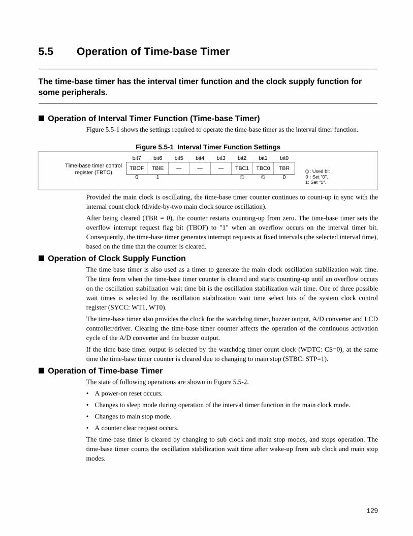
5.5 Operation of Time-base Timer
The time-base timer has the interval timer function and the clock supply function for some peripherals.
Operation of Interval Timer Function (Time-base Timer)Figure 5.5-1 shows the settings required to operate the time-base timer as the interval timer function.
Figure 5.5-1 Interval Timer Function Settings
Provided the main clock is oscillating, the time-base timer counter continues to count-up in sync with the
internal count clock (divide-by-two main clock source oscillation).
After being cleared (TBR = 0), the counter restarts counting-up from zero. The time-base timer sets the
overflow interrupt request flag bit (TBOF) to "1" when an overflow occurs on the interval timer bit.
Consequently, the time-base timer generates interrupt requests at fixed intervals (the selected interval time),
based on the time that the counter is cleared.
Operation of Clock Supply FunctionThe time-base timer is also used as a timer to generate the main clock oscillation stabilization wait time.
The time from when the time-base timer counter is cleared and starts counting-up until an overflow occurs
on the oscillation stabilization wait time bit is the oscillation stabilization wait time. One of three possible
wait times is selected by the oscillation stabilization wait time select bits of the system clock control
register (SYCC: WT1, WT0).
The time-base timer also provides the clock for the watchdog timer, buzzer output, A/D converter and LCD
controller/driver. Clearing the time-base timer counter affects the operation of the continuous activation
cycle of the A/D converter and the buzzer output.
If the time-base timer output is selected by the watchdog timer count clock (WDTC: CS=0), at the same
time the time-base timer counter is cleared due to changing to main stop (STBC: STP=1).
Operation of Time-base TimerThe state of following operations are shown in Figure 5.5-2.
• A power-on reset occurs.
• Changes to sleep mode during operation of the interval timer function in the main clock mode.
• Changes to main stop mode.
• A counter clear request occurs.
The time-base timer is cleared by changing to sub clock and main stop modes, and stops operation. The
time-base timer counts the oscillation stabilization wait time after wake-up from sub clock and main stop
modes.
Time-base timer control register (TBTC)
bit7 bit6 bit5 bit4 bit3 bit2 bit1 bit0
TBOF TBIE — — — TBC1 TBC0 TBR
0 1 0: Used bit
0 : Set "0". 1: Set "1".
129

CHAPTER 5 TIME-BASE TIMER
Figure 5.5-2 Operation of Time-base Timer
Counter value1FFFFFH
Oscillation stabilization wait overflow
00000H
Power-on reset
CPU operation starts Interval cycle (TBTC: TBC1, TBC0 = 11B)
Cleared by the interrupt processing routine.
Cleared by changing to main stop mode.
Counter clear (TBTC: TBR = 0)
TBOF bit
TBIE bit
SLP bit(STBC register)
STP bit (STBC register)
Sleep mode
Wake-up from Sleep mode by IRQB
Stop mode
Wake-up from Stop mode by an external interrupt
: Indicates the oscillation stabilization wait time.
For the case when the interval time selection bits in the time-base timer control register
(TBTC: TBC1, TBC0) are set to "11B" (222/FCH).
130

5.6 Notes on Using Time-base Timer
This section lists points to note when using the time-base timer.
Notes on Using Time-base Timer
Notes on setting bits by program
The system cannot recover from interrupt processing if the overflow interrupt request flag bit (TBTC:
TBOF) is "1" and the interrupt request enable bit is enabled (TBTC: TBIE = 1). Always clear the TBOF bit.
Clearing time-base timer
In addition to being cleared by the time-base timer initialization bit (TBTC: TBR = 0), the timer is cleared
whenever the main clock oscillation stabilization wait time is required. When the time-base timer is
selected as a count clock of the watchdog timer, clearing the time-base timer also clears the watchdog
timer.
Using as timer for oscillation stabilization wait time
As the main clock source oscillation is stopped when the power is turned on during main-stop mode, the
time-base timer provides the main clock oscillation stabilization wait time after the oscillator starts.
An appropriate oscillation stabilization wait time must be selected for the type of resonator connected to the
main clock oscillator (clock generator).
See "3.6.5 Oscillation Stabilization Wait Time".
Notes on peripheral functions that provided a clock supply from time-base timer
In modes in which the main clock source oscillation is stopped, the time-base timer also stops, and the
counter is cleared.
As the clock derived from the time-base timer restarts output from its initial state when the time-base timer
counter is cleared, the "H" level may be shorter or the "L" level longer by a maximum of half cycle. The
clock of the watchdog timer also restarts output from its initial state.
Figure 5.6-1 shows the effect on the buzzer output of clearing the time-base timer.
131

CHAPTER 5 TIME-BASE TIMER
Figure 5.6-1 Effect on Buzzer Output of Clearing Time-base Timer
Counter value (bit11:0)
00FFFH
00800H
00000H
Clock supplied to the buzzer output
For the case when the buzzer selection bits in the buzzer register (BUZR: BZ2, BZ1, BZ0) are set to "001B". (Divide-by-4096 main source oscillation, approximately 3.051 kHz output at 12.5 MHz operation)
Clearing the counter by the program (TBTC: TBR = 0)
132

5.7 Program Example for Time-base Timer
This section gives a program example for the time-base timer.
Program Example for Time-base Timer
Processing description
Generates repeated interval timer interrupts at 218/FCH (FCH: the main clock source oscillation) intervals.
At this time, the interval time is set to approximately 26.2 ms (FCH: at 10 MHz operation).
Coding example
TBTC EQU 0000AH ; Address of the time-base timer control register
TBOF EQU TBTC:7 ; Define the interrupt request flag bit.
ILR3 EQU 007DH ; Address of the interrupt level setting register 3
INT_V DSEG ABS ; [DATA SEGMENT]ORG 0FFE4H
IRQB DW WARI ; Set interrupt vector.INT_V ENDS;-----Main program---------------------------------------------------------------------------------------------------------------------------------------
CSEG ; [CODE SEGMENT]; Stack pointer (SP) etc. are already initialized.
:CLRI ; Disable interrupts.MOV ILR3,#01111111B ; Set interrupt level (level 1).MOV TBTC,#01000100B ; Clear interrupt request flag enable interrupt request output,
select 218/FCH, and clear time-base timer.SETI ; Enable interrupts.
:;-----Interrupt program----------------------------------------------------------------------------------------------------------------------------------WARI CLRB TBOF ; Clear interrupt request flag.
PUSHW AXCHW A,TPUSHW A
:User processing
:POPW AXCHW A,TPOPW ARETIENDS
;--------------------------------------------------------------------------------------------------------------------------------------------------------------END
133

CHAPTER 5 TIME-BASE TIMER
134
CHAPTER 6WATCHDOG TIMER
This chapter describes the functions and operation of the watchdog timer.
6.1 Overview of Watchdog Timer
6.2 Block Diagram of Watchdog Timer
6.3 Watchdog Timer Control Register (WDTC)
6.4 Operation of Watchdog Timer
6.5 Notes on Using Watchdog Timer
6.6 Program Example for Watchdog Timer
135

CHAPTER 6 WATCHDOG TIMER
6.1 Overview of Watchdog Timer
The watchdog timer is a 1-bit counter that uses, as its count clock source, either the time-base timer derived from the main clock, or the watch prescaler derived from the sub clock. The watchdog timer resets the CPU if not cleared within a fixed time after activation.
Watchdog Timer Function• The watchdog timer is a counter provided to guard against program runaway. Once activated, the
counter must be repeatedly cleared within a fixed time interval. If the program becomes trapped in anendless loop or similar and does not clear the counter within the fixed time, the watchdog timergenerates a four-instruction cycle watchdog reset to the CPU.
• Either the time-base timer output or the watch prescaler output can be selected as the watchdog timercount clock.
• Table 6.1-1 lists the watchdog timer interval times. If not cleared, the watchdog timer generates awatchdog reset at a time between the minimum and maximum times listed. Clear the counter within theminimum time given in the table below.
See "6.4 Operation of Watchdog Timer" for the details on the minimum and maximum time of the
watchdog timer interval times".
Reference:
The watchdog timer counter is cleared whenever the device changes to sleep, stop or watch mode.Operation halts until the device returns to normal operation (RUN state).
Table 6.1-1 Watchdog Timer Interval Time
Count clock
Time-base timer output (main clock oscillator frequency at 12.5 MHz)
Watch prescaler output (sub clock oscillator frequency at 32.768 kHz)
Minimum time Approx. 335.5 ms*1 500 ms*2
Maximum time Approx. 671 ms 1000 ms
*1: Divide-by-two the main clock source oscillation (FCH) × time-base timer count value (221).
*2: The time of a clock cycle at the sub clock oscillator frequency (FCL) × watch prescaler count (214).
136

6.2 Block Diagram of Watchdog Timer
The watchdog timer consists of the following six blocks:• Count clock selector• Watchdog timer counter• Reset controller• Watchdog timer clear selector• Counter clear controller• Watchdog timer control register (WDTC)
Block Diagram of Watchdog Timer
Figure 6.2-1 Block Diagram of Watchdog Timer
Count clock selector
The count clock selector selects the count clock for the watchdog timer counter. Either the time-base timer
output or the watch prescaler output can be selected as the count clock.
Watchdog timer counter (1-bit counter)
A 1-bit counter that uses the time-base timer output or the watch prescaler output as a count clock.
CS — — — WTE3 WTE2 WTE1 WTE0
WDTC register
Counter clear
Watchdog timer
1-bit counter RSTReset controller
controller
clear selector
222/FCH (time-base timer output)
214/FCL (watch prescaler out-put)
Count clock selector
Overflow
Watchdog timer
StartClear
Sleep mode startStop mode start
Watch mode start
FCH: main clock source oscillationFCL: sub clock source oscillation
Clear signal from time-base timer
Clear signal from watch prescaler
137

CHAPTER 6 WATCHDOG TIMER
Reset controller
Generates a reset signal to the CPU when an overflow occurs on the watchdog timer counter.
Watchdog timer clear selector
The watchdog timer clear selector selects a watchdog timer clear signal from either the time-base timer or
watch prescaler at the same time as the count clock selector selects a clock. (It selects the clear signal from
the selected clock source.)
Counter clear controller
Controls clearing, activating, and halting the operation of watchdog timer counter.
Watchdog timer control register (WDTC)
The WDTC register is used to select the count clock, and to activate or clear the watchdog timer counter.
As the register is write-only, the bit manipulation instructions cannot be used.
138
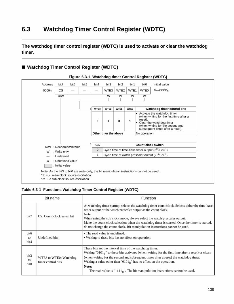
6.3 Watchdog Timer Control Register (WDTC)
The watchdog timer control register (WDTC) is used to activate or clear the watchdog timer.
Watchdog Timer Control Register (WDTC)
Figure 6.3-1 Watchdog timer Control Register (WDTC)
Table 6.3-1 Functions Watchdog Timer Control Register (WDTC)
Bit name Function
bit7 CS: Count clock select bit
At watchdog timer startup, selects the watchdog timer count clock. Selects either the time-base timer output or the watch prescaler output as the count clock.Note:When using the sub clock mode, always select the watch prescaler output.Make the count clock selection when the watchdog timer is started. Once the timer is started, do not change the count clock. Bit manipulation instructions cannot be used.
bit6to
bit4Undefined bits
• The read value is undefined.• Writing to these bits has no effect on operation.
bit3to
bit0
WTE3 to WTE0: Watchdog timer control bits
These bits set the interval time of the watchdog timer.Writing "0101B" to these bits activates (when writing for the first time after a reset) or clears
(when writing for the second and subsequent times after a reset) the watchdog timer. Writing a value other than "0101B" has no effect on the operation.
Note:The read value is "1111B". The bit manipulation instructions cannot be used.
Address bit7 bit6 bit5 bit4 bit3 bit2 bit1 bit0 Initial value
0009H CS — — — WTE3 WTE2 WTE1 WTE0 0---XXXXB
R/W W W W W
WTE3 WTE2 WTE1 WTE0 Watchdog timer control bits
0 1 0 1
• Activate the watchdog timer (when writing for the first time after a reset).
• Clear the watchdog timer (when writing for the second and subsequent times after a reset).
Other than the above No operation
CS Count clock switch
0 Cycle time of time-base timer output (222/FCH*1)
1 Cycle time of watch prescaler output (214/FCL*2)
Note: As the bit3 to bit0 are write-only, the bit manipulation instructions cannot be used.*1: FCH: main clock source oscillation*2: FCL: sub clock source oscillation
R/W : Readable/Writable
W : Write only
— : Undefined
X : Undefined value
: Initial value
139

CHAPTER 6 WATCHDOG TIMER
6.4 Operation of Watchdog Timer
The watchdog timer generates a watchdog reset when the watchdog timer counter overflows.
Operation of Watchdog Timer
Activating watchdog timer
• The watchdog timer is activated by writing "0101B" to the watchdog control bits in the watchdog
control register (WDTC: WTE3 to WTE0) for the first time after a reset.
• The count clock switch bit (WDTC: CS) is written to the desired state in the same write operation.
• Once activated, the watchdog timer cannot be stopped other than by a reset.
Clearing watchdog timer
• The watchdog timer counter is cleared by writing "0101B" to the watchdog control bits in the watchdog
control register (WDTC: WTE3 to WTE0) for the second or subsequent times after a reset.
• If the counter is not cleared within the interval time of the watchdog timer, the counter overflows and
the watchdog timer generates an internal reset signal for four-instruction cycles.
Interval time of watchdog timer
The interval time changes depending on the watchdog timer clear timing.
Figure 6.4-1 shows the relationship between the watchdog timer clear timing and the interval time.
The indicated times apply if the time-base timer output is selected as the count clock, and the main clock
source oscillation is 12.5 MHz.
140

Figure 6.4-1 Watchdog Timer Clear and Interval Time
Minimum time
Count clock output of the time-base timer
Watchdog clear Overflow
1-bit watchdog counter
Watchdog reset
Maximum time
Watchdog clear Overflow
Count clock output of the time-base timer
1-bit watchdog counter
Watchdog reset
335.5ms
671 ms
141
CHAPTER 6 WATCHDOG TIMER
6.5 Notes on Using Watchdog Timer
This section lists points to note when using the watchdog timer.
Notes on Using Watchdog Timer
Stopping watchdog timer
Once activated, the watchdog timer cannot stop until a reset generates.
Count clock selection
The count clock select bit (WDTC: CS) can only be changed writing "0101B" to the watchdog control bits
(WDTC: WTE3 to WTE0) to activate the watchdog timer. Therefore, the CS bit cannot be changed by a bit
operation instruction. Do not change the CS bit after activating the timer.
In the sub clock mode, the main clock source oscillation is stopped, which means that the time-base timer
also stops. For the watchdog timer to operate in sub clock mode, then, the watch prescaler must have been
selected in advance as the count clock (WDTC: CS = 1).
Clearing watchdog timer
• Clearing the counter being used as a count clock of the watchdog timer (time-base timer or watch
prescaler) also simultaneously clears the watchdog timer counter.
• The watchdog timer counter is cleared on changing to sleep, stop or watch mode.
Notes on programming
When writing a program in which the watchdog timer is repeatedly cleared in the main loop, the processing
time for the main loop including interrupt processing must be less than the minimum watchdog timer
interval time.
Operation in sub clock mode
If the watchdog reset signal is generated in sub clock mode, operation will start in main clock mode after an
oscillation stabilization wait time. Therefore, a reset signal will be output during the oscillation stabilization
wait time.
142

6.6 Program Example for Watchdog Timer
This section gives a program example for the watchdog timer.
Program Example for Watchdog Timer
Processing description
• Selects the watch prescaler as the count clock and activates the watchdog timer immediately after the
program.
• Clears the watchdog timer in each loop of the main program.
• The processing time for the main loop, including interrupt processing, must be less than the minimum
interval time of the watchdog timer (approximately 500 ms at 32.768 KHz operation).
Coding example
WDTC EQU 00009H ; Address of the watchdog timer control registerWDT_CLR EQU 10000101B
VECT DSEG ABS ; [DATA SEGMENT]ORG 0FFFEH
RST_V DW PROG ; Set reset vector.VECT ENDS;-----Main program---------------------------------------------------------------------------------------------------------------------------------------
CSEG ; [CODE SEGMENT]PROG ; Initialization routine after a reset
MOVW SP,#0280H ; Set initial value of (for interrupt processing).:
Initialization of peripheral functions (interrupts), etc.:
INIT MOV WDTC,#WDT_CLR ; Activate the watchdog timer.
: ; Select the watch prescaler as the count clock.MAIN MOV WDTC,#WDT_CLR ; Clear the watchdog timer.
:User processing (interrupt processing may occur during this cycle)
:
JMP MAIN; The loop must be executed in less than the minimum interval time of the watchdog timer.
ENDS;--------------------------------------------------------------------------------------------------------------------------------------------------------------
END
143

CHAPTER 6 WATCHDOG TIMER
144
CHAPTER 7WATCH PRESCALER
This chapter describes the functions and operation of the watch prescaler.
7.1 Overview of Watch Prescaler
7.2 Block Diagram of Watch Prescaler
7.3 Watch Prescaler Control Register (WPCR)
7.4 Watch Prescaler Interrupt
7.5 Operation of Watch Prescaler
7.6 Notes on Using Watch Prescaler
7.7 Program Example for Watch Prescaler
145

CHAPTER 7 WATCH PRESCALER
7.1 Overview of Watch Prescaler
The watch prescaler provides interval timer functions. Six different interval times can be selected. The watch prescaler uses a 17-bit free-run counter which counts-up in sync with a sub clock generated by the clock generator. The watch prescaler also provides the timer output for the sub clock oscillation stabilization wait time and the operating clock for watchdog timer and buzzer output.
Interval Timer Function (Watch Interrupt)• The interval timer function generates repeated interrupts at fixed intervals with the sub clock used as the
count clock.
• Interrupts are generated by watch prescaler interval timer divided clock outputs.
• The interval timer divided clock output (interval time) can be selected from different settings.
• The watch prescaler counter can be cleared.
Table 7.1-1 lists the available interval times for the watch prescaler.
Note:
The watch prescaler cannot be used in devices in which a single clock option has been selected.
Table 7.1-1 Watch Prescaler Interval Time
Sub clock Cycle Time Interval time
1/FCL (approx. 30.5 µs)
210/FCL (31.25 ms)
213/FCL (0.25 s)
214/FCL (0.50 s)
215/FCL (1.00 s)
216/FCL (2.00 s)
217/FCL (4.00 s)
FCL: Sub clock source oscillation
The values enclosed in parentheses are for a 32.768 kHz sub clock source oscillation.
146

Clock Supply FunctionThe watch prescaler has the following clock supply functions:
• The timer output used for the sub clock oscillation stabilization wait time (one value)
• The clock used for the watchdog timer (one value)
• The clock used for the buzzer output (three values)
Table 7.1-2 lists the cycles of the clocks that the watch prescaler supplies to various peripherals.
Note:
The oscillation stabilization wait time should be used as a guideline since the oscillation cycle isunstable immediately after oscillation starts.
Table 7.1-2 Clocks Supplied by Watch Prescaler
Sub clock destination Sub clock cycle Remarks
Sub clock oscillation stabilization wait time
215/FCL (1.00 s) Do not switch to the sub clock mode during the oscillation stabilization wait time.
Watchdog timer 214/FCL (0.50 s) Count-up clock for the watchdog timer
Buzzer output 23/FCL to 25/FCL
(approx. 0.24 to 0.98 ms)
See "CHAPTER 16 BUZZER OUTPUT".
FCL: Sub clock source oscillationThe values enclosed in parentheses are for a 32.768 kHz sub clock source oscillation.
147
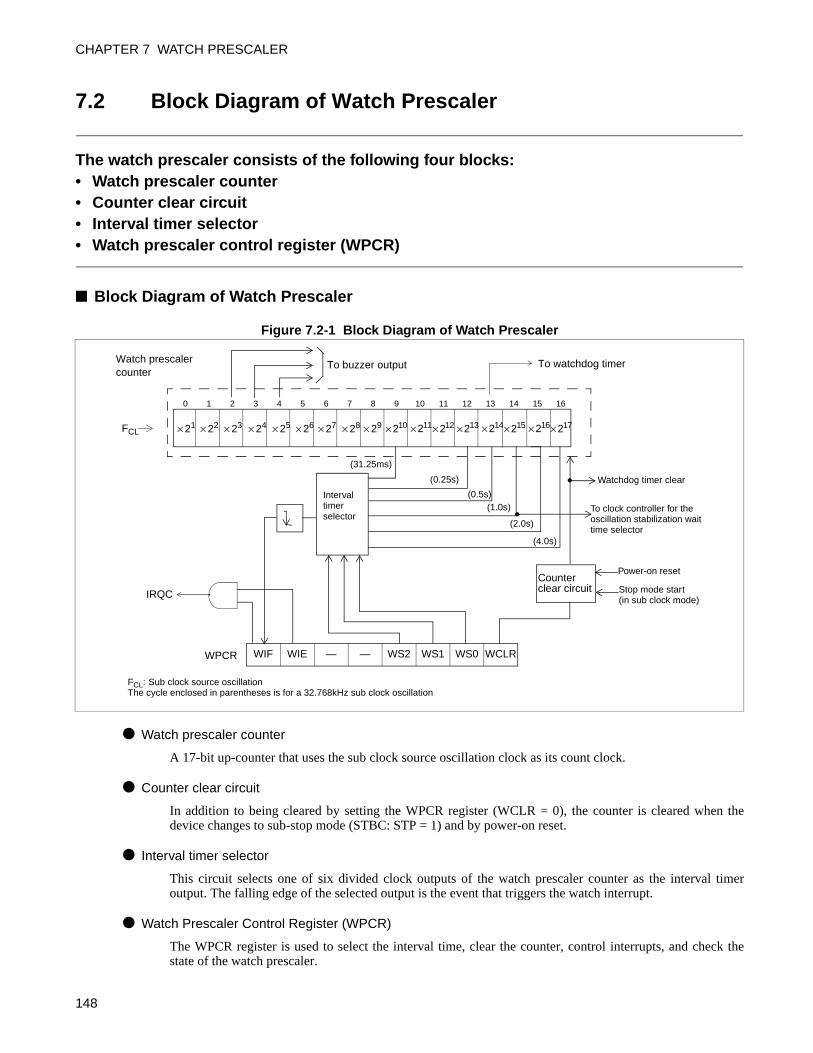
CHAPTER 7 WATCH PRESCALER
7.2 Block Diagram of Watch Prescaler
The watch prescaler consists of the following four blocks:• Watch prescaler counter• Counter clear circuit• Interval timer selector• Watch prescaler control register (WPCR)
Block Diagram of Watch Prescaler
Figure 7.2-1 Block Diagram of Watch Prescaler
Watch prescaler counter
A 17-bit up-counter that uses the sub clock source oscillation clock as its count clock.
Counter clear circuit
In addition to being cleared by setting the WPCR register (WCLR = 0), the counter is cleared when thedevice changes to sub-stop mode (STBC: STP = 1) and by power-on reset.
Interval timer selector
This circuit selects one of six divided clock outputs of the watch prescaler counter as the interval timeroutput. The falling edge of the selected output is the event that triggers the watch interrupt.
Watch Prescaler Control Register (WPCR)
The WPCR register is used to select the interval time, clear the counter, control interrupts, and check thestate of the watch prescaler.
WIF WIE — — WS2 WS1 WS0 WCLRWPCR
FCL
FCL: Sub clock source oscillationThe cycle enclosed in parentheses is for a 32.768kHz sub clock oscillation
Counter clear circuit
To watchdog timer
× 21 × 22 × 23 × 24 × 25 × 26 × 27 × 28 × 29 ×210 ×211×212 ×213 ×214×215 ×216× 217
0 1 2 3 4 5 6 7 8 9 10 11 12 13 14 15 16
IRQC
Interval timer selector
Watchdog timer clear
To clock controller for the oscillation stabilization wait time selector
Power-on reset
Stop mode start(in sub clock mode)
(0.5s)(1.0s)
(2.0s)
(4.0s)
(0.25s)
(31.25ms)
To buzzer outputWatch prescalercounter
148
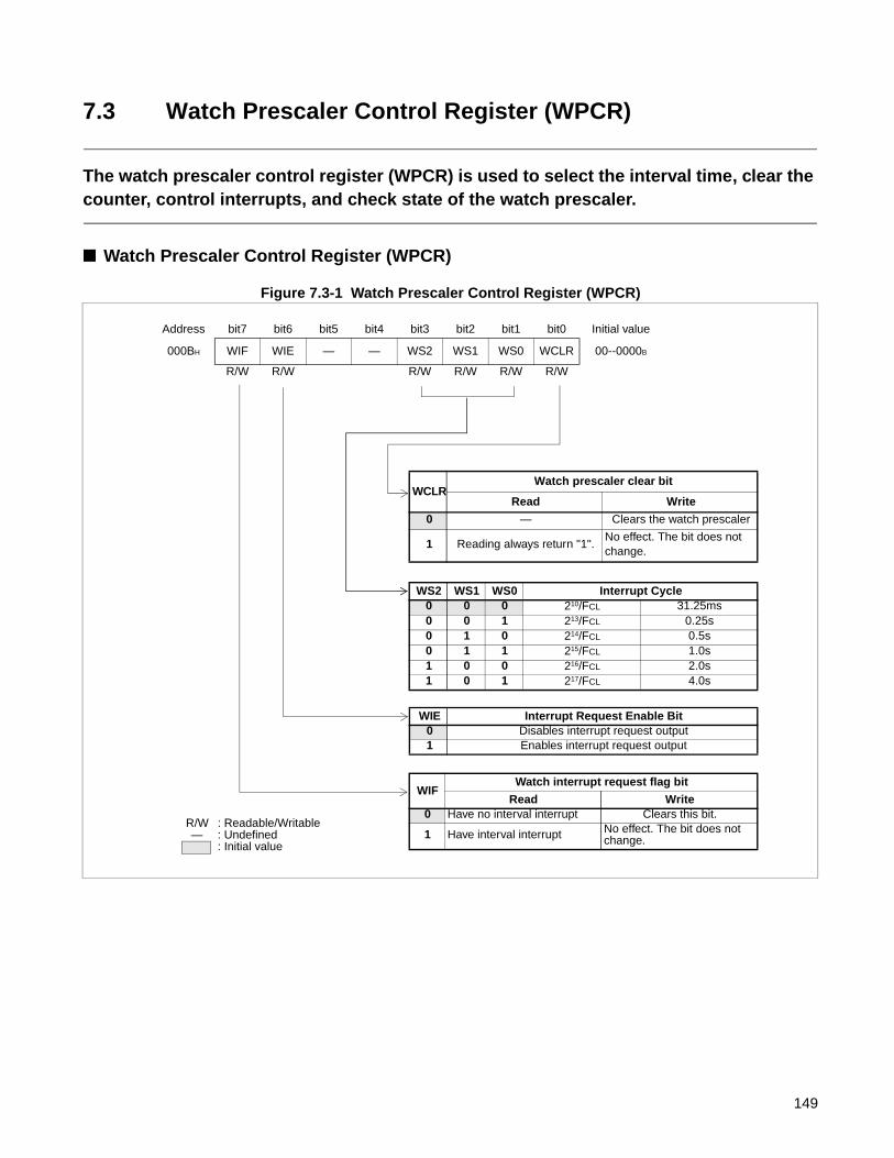
7.3 Watch Prescaler Control Register (WPCR)
The watch prescaler control register (WPCR) is used to select the interval time, clear the counter, control interrupts, and check state of the watch prescaler.
Watch Prescaler Control Register (WPCR)
Figure 7.3-1 Watch Prescaler Control Register (WPCR)
Address bit7 bit6 bit5 bit4 bit3 bit2 bit1 bit0 Initial value
000BH WIF WIE — — WS2 WS1 WS0 WCLR 00--0000B
R/W R/W R/W R/W R/W R/W
WCLRWatch prescaler clear bit
Read Write
0 — Clears the watch prescaler
1 Reading always return "1". No effect. The bit does not change.
WS2 WS1 WS0 Interrupt Cycle0 0 0 210/FCL 31.25ms0 0 1 213/FCL 0.25s0 1 0 214/FCL 0.5s0 1 1 215/FCL 1.0s1 0 0 216/FCL 2.0s1 0 1 217/FCL 4.0s
WIE Interrupt Request Enable Bit0 Disables interrupt request output1 Enables interrupt request output
WIFWatch interrupt request flag bit
Read Write0 Have no interval interrupt Clears this bit.
1 Have interval interrupt No effect. The bit does not change.
R/W : Readable/Writable— : Undefined
: Initial value
149
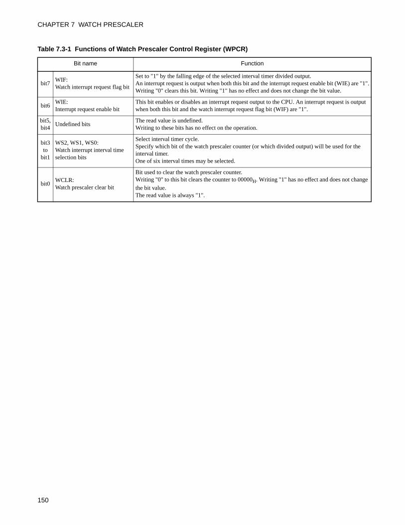
CHAPTER 7 WATCH PRESCALER
Table 7.3-1 Functions of Watch Prescaler Control Register (WPCR)
Bit name Function
bit7WIF: Watch interrupt request flag bit
Set to "1" by the falling edge of the selected interval timer divided output.An interrupt request is output when both this bit and the interrupt request enable bit (WIE) are "1".Writing "0" clears this bit. Writing "1" has no effect and does not change the bit value.
bit6WIE: Interrupt request enable bit
This bit enables or disables an interrupt request output to the CPU. An interrupt request is output when both this bit and the watch interrupt request flag bit (WIF) are "1".
bit5,bit4
Undefined bitsThe read value is undefined.Writing to these bits has no effect on the operation.
bit3to
bit1
WS2, WS1, WS0: Watch interrupt interval time selection bits
Select interval timer cycle.Specify which bit of the watch prescaler counter (or which divided output) will be used for the interval timer.One of six interval times may be selected.
bit0WCLR:Watch prescaler clear bit
Bit used to clear the watch prescaler counter.Writing "0" to this bit clears the counter to 00000H. Writing "1" has no effect and does not change
the bit value.The read value is always "1".
150
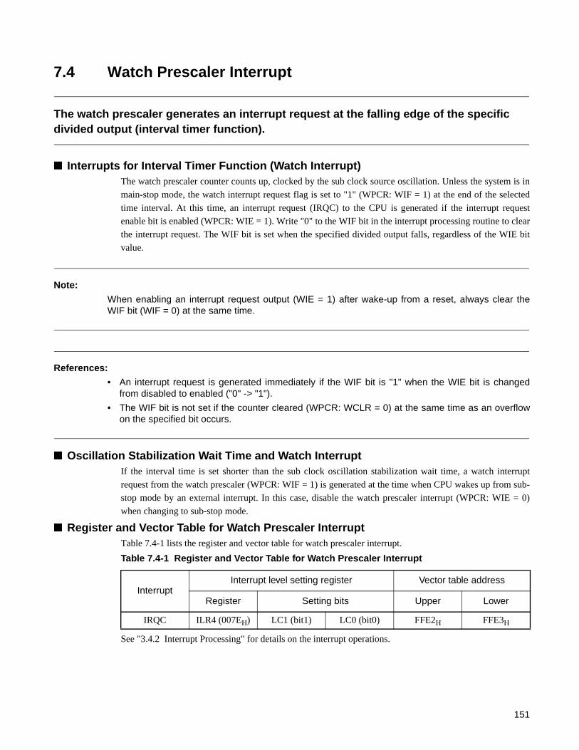
7.4 Watch Prescaler Interrupt
The watch prescaler generates an interrupt request at the falling edge of the specific divided output (interval timer function).
Interrupts for Interval Timer Function (Watch Interrupt)The watch prescaler counter counts up, clocked by the sub clock source oscillation. Unless the system is in
main-stop mode, the watch interrupt request flag is set to "1" (WPCR: WIF = 1) at the end of the selected
time interval. At this time, an interrupt request (IRQC) to the CPU is generated if the interrupt request
enable bit is enabled (WPCR: WIE = 1). Write "0" to the WIF bit in the interrupt processing routine to clear
the interrupt request. The WIF bit is set when the specified divided output falls, regardless of the WIE bit
value.
Note:
When enabling an interrupt request output (WIE = 1) after wake-up from a reset, always clear theWIF bit (WIF = 0) at the same time.
References:
• An interrupt request is generated immediately if the WIF bit is "1" when the WIE bit is changedfrom disabled to enabled ("0" -> "1").
• The WIF bit is not set if the counter cleared (WPCR: WCLR = 0) at the same time as an overflowon the specified bit occurs.
Oscillation Stabilization Wait Time and Watch InterruptIf the interval time is set shorter than the sub clock oscillation stabilization wait time, a watch interrupt
request from the watch prescaler (WPCR: WIF = 1) is generated at the time when CPU wakes up from sub-
stop mode by an external interrupt. In this case, disable the watch prescaler interrupt (WPCR: WIE = 0)
when changing to sub-stop mode.
Register and Vector Table for Watch Prescaler InterruptTable 7.4-1 lists the register and vector table for watch prescaler interrupt.
See "3.4.2 Interrupt Processing" for details on the interrupt operations.
Table 7.4-1 Register and Vector Table for Watch Prescaler Interrupt
InterruptInterrupt level setting register Vector table address
Register Setting bits Upper Lower
IRQC ILR4 (007EH) LC1 (bit1) LC0 (bit0) FFE2H FFE3H
151

CHAPTER 7 WATCH PRESCALER
7.5 Operation of Watch Prescaler
The watch prescaler has the interval timer function and the clock supply function.
Operation of Interval Timer Function (Watch Prescaler)Figure 7.5-1 shows the settings required to operate as the interval timer function.
Figure 7.5-1 Interval Timer Function Settings
Provided the sub clock is oscillating, the watch prescaler 17-bit counter continues to count-up using the sub
clock as its count clock.
After being cleared (WCLR = 0), the counter restarts counting-up from "00000H". When the counter
reaches a full count of "1FFFFH", the next count takes it "00000H", and it continues to count-up. As the
count proceeds, a falling edge will eventually occur at the selected divided clock output. At this time,
unless the system is in main stop mode, the watch prescaler sets the watch interrupt request flag bit (WIF)
to "1". Consequently, the watch prescaler generates watch interrupt requests at fixed intervals (the selected
interval time), based on the time that the counter is cleared.
Operation of Clock supply Function The watch prescaler is also used as a timer to generate the sub clock oscillation stabilization wait time. The
time between the counter cleared state and the falling edge of the MSB output is used the sub clock
oscillation stabilization wait time (215/FCL, where FCL is sub clock source oscillation).
The watch prescaler also provides the clock for the watchdog timer and buzzer output. Clearing the
watchdog timer counter affects the operation of the buzzer output. When the watch prescaler is selected as
the clock source for the watchdog timer (WDTC: CS = 1) both counters are cleared simultaneously.
bit7 bit6 bit5 bit4 bit3 bit2 bit1 bit0
WPCR WIF WIE — — WS2 WS1 WS0 WCLR
0 1 0: Used bit
1: Set "1"0: Set "0"
152
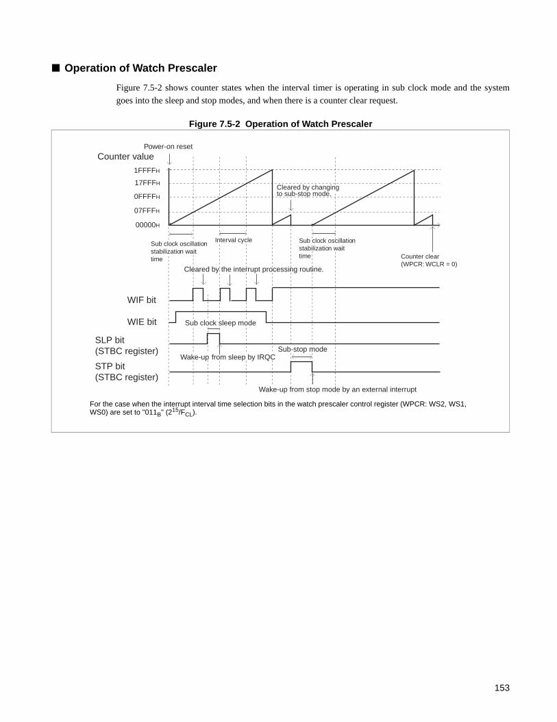
Operation of Watch Prescaler
Figure 7.5-2 shows counter states when the interval timer is operating in sub clock mode and the system
goes into the sleep and stop modes, and when there is a counter clear request.
Figure 7.5-2 Operation of Watch Prescaler
1FFFFH
00000H
Counter value
Cleared by changingto sub-stop mode.
Sub clock oscillation stabilization waittime
Interval cycle Sub clock oscillation stabilization waittime Counter clear
(WPCR: WCLR = 0)Cleared by the interrupt processing routine.
WIF bit
WIE bit
SLP bit (STBC register)
Sub clock sleep mode
STP bit (STBC register)
Wake-up from sleep by IRQCSub-stop mode
Wake-up from stop mode by an external interrupt
0FFFFH
Power-on reset
17FFFH
07FFFH
For the case when the interrupt interval time selection bits in the watch prescaler control register (WPCR: WS2, WS1, WS0) are set to "011B" (215/FCL).
153
CHAPTER 7 WATCH PRESCALER
7.6 Notes on Using Watch Prescaler
This section lists points to note when using the watch prescaler. The watch prescaler cannot be used in devices in which the single-clock option has been selected.
Notes on Using Watch Prescaler
Notes on setting bits by program
The system cannot recover from interrupt processing if the interrupt request flag bit (WPCR: WIF) is "1"
and the interrupt request enable bit is enabled (WPCR: WIE = 1). Always clear the WIF bit.
Clearing Watch prescaler
In addition to being cleared by the watch prescaler clear bit (WPCR: WCLR = 0), the watch prescaler is
cleared wherever the sub clock oscillation stabilization wait time is required.
When the watch prescaler is selected as a count clock of the watchdog timer (WDTC: CS = 1), clearing the
watch prescaler also clears the watchdog timer.
Using as timer for oscillation stabilization wait time
As the sub clock source oscillation is stopped when the power is turned on and during sub-stop mode, the
watch prescaler provides the oscillation stabilization wait time after the oscillator starts. Do not switch
clock modes from main clock to sub clock during this wait time (immediately after power on, etc.)
The sub clock oscillation stabilization wait time is fixed.
See "3.6.5 Oscillation Stabilization Wait Time" for details.
Notes on watch interrupt
In main-stop mode, the watch prescaler counter operates, but no watch interrupt is generated.
Notes on peripheral functions that provides a clock supply from watch prescaler
As the clock derived from the watch prescaler restarts output from the its initial state when the watch
prescaler counter is cleared, the "H" level may be shorter or the "L" level longer by a maximum of half
cycle. The clock of the watchdog timer also restarts output from its initial state. However, as the watchdog
timer counter is cleared at the same time, the watchdog timer operates in normal cycle.
Figure 7.6-1 shows the effect on the buzzer output of clearing the watch prescaler.
154

Figure 7.6-1 Effect on Buzzer Output Due to Clearing of Watch Prescaler
001FH
0010H
0000H
Counter value (bit4:0)
Clearing the counter by the program (WPCR: WCLR = 0)
Clock supplied to the buzzer output
For the case when the buzzer selection bits in the buzzer register (BUZR: BZ2, BZ1, BZ0) are set to "101B".(Divide-by-32 sub clock source oscillation, 1024 Hz output at 32.768 kHz operation).
155
CHAPTER 7 WATCH PRESCALER
7.7 Program Example for Watch Prescaler
This section gives program example for the watch prescaler.
Program Example for the Watch Prescaler
Processing description
Generates repeated watch interrupts at 215/FCL (FCL = sub clock source oscillation) intervals. At this time,
the interval time is 1 second (at 32.768 kHz operation).
Coding example
WPCR EQU 000BH ; Address of watch prescaler control register
WIF EQU WPCR:7 ; Define the watch interrupt request flag bit.
ILR4 EQU 007EH ; Address of the interrupt level setting register 2
INT_V DSEG ABS ; [DATA SEGMENT]
ORG 0FFE2H
IRQC DW WARI ; Set interrupt vector.
INT_V ENDS
;------------ Main program ------------------------------------------------------------------------------------------
CSEG ; [CODE SEGMENT]
; Stack pointer (SP) etc. are already initialized.
:
CLRI ; Disable interrupts.
MOV ILR4, #11111110B ; Set interrupt priority (level 2).
MOV WPCR, #01000110B ; Clear interrupt request flag, enable interrupt request output, select
215/FCL, and clear watch prescaler.
SETI ; Enable interrupts.
:
;------------ Interrupt program ------------------------------------------------------------------------------------------
WARI CLRB WIF ; Clear interrupt request flag.
PUSHWA
XCHW A,T
PUSHWA
:
User processing
:
POPW A
XCHW A,T
POPW A
RETI
ENDS
;-------------------------------------------------------------------------------------------------------------------------------
END
156

CHAPTER 88-BIT PWM TIMER
This chapter describes the functions and operation of the 8-bit PWM timer.
8.1 Overview of 8-bit PWM Timer
8.2 Block Diagram of 8-bit PWM Timer
8.3 Structure of 8-bit PWM Timer
8.4 Registers of 8-bit PWM Timer
8.5 8-bit PWM Timer Interrupts
8.6 Operation of Interval Timer Function
8.7 Operation of PWM Timer Function
8.8 States in Each Mode during 8-bit PWM Timer Operation
8.9 Notes on Using 8-bit PWM Timer
8.10 Program Example for 8-bit PWM Timer
157

CHAPTER 8 8-BIT PWM TIMER
8.1 Overview of 8-bit PWM Timer
The 8-bit PWM timer can be selected to function as either an interval timer or PWM timer with 8-bit resolution. The interval timer function counts-up in sync with one of four internal count clocks. Therefore, an 8-bit interval timer time can be set and the output can be used to generate variable frequency square waves. Also, the 8-bit PWM timer can be used as a D/A converter by connecting the PWM output to low pass filter.
Interval Timer Function (Square Wave Output Function)The interval timer function generates repeated interrupts at variable time intervals.
Also, as the 8-bit PWM timer can invert the output level of the pin (PWM) each time an interrupt is
generated, the 8-bit PWM timer can output a variable frequency square waves.
• The interval timer can operate with a cycle among 1 and 28 times the count clock cycle.
• The count clock can be selected from four different clocks.
Table 8.1-1 lists the range for the interval time and square wave output.
[Calculation example for the interval time and square wave frequency]
In this example, the main clock source oscillation (FCH) is 12.5 MHz, the PWM compare register (COMR)
value is set to "DDH (221)", and the count clock cycle is set to 1 tinst. In this case, the interval time and the
frequency of the square wave output from the PWM pin (where the PWM timer operates continuously and
the value of the COMR register is constant) are calculated as follows.
Assume that the main clock mode and its highest clock speed has been selected via the system clock
control register (SYCC: SCS = 1, CS1 = 1, CS0 = 1, 1 instruction cycle = 4/FCH).
Interval time = (1 × 4/FCH) × (COMR register value + 1)
= (4/12.5 MHz) × (221 + 1)
= 71.04 µs
Output frequency = FCH/(1 × 8 × (COMR register value +1))
= 12.5 MHz/(8 × (221 + 1))
= approx. 7.04 kHz
Table 8.1-1 Interval Time and Square Wave Output Range
Count clock cycle Interval time Square wave output (Hz)
1
Internal count clock
1 tinst 1 tinst to 28 tinst 1/(2 tinst) to 1/(29 tinst)
2 8 tinst 23 tinst to 211 tinst 1/(24 tinst) to 1/(212 tinst)
3 16tinst 24 tinst to 212 tinst 1/(25 tinst) to 1/(213 tinst)
4 64 tinst 26 tinst to 214 tinst 1/(27 tinst) to 1/(215 tinst)
tinst: Instruction cycle (affected by clock mode, etc.)
158

PWM Timer FunctionThe PWM timer function has 8-bit resolution and can control the "H" and "L" widths of one cycle.
• As the resolution is 1/256, pulses can be output with duty ratios between 0 and 99.6%.
• The cycle of the PWM wave can be selected from four types.
• The PWM timer can be used as a D/A converter by connecting the output to a low pass filter.
Table 8.1-2 lists the available PWM wave cycles for the PWM timer function. Figure 8.1-1 shows a
configuration example of D/A converter.
Figure 8.1-1 Configuration Example of D/A Converter Using PWM Output and Low Pass Filter
Note:
Interrupt requests are not generated during operation of the PWM function.
Table 8.1-2 Available PWM Wave Cycle for PWM Timer Function
1 2 3 4
Internal count clock
Count clock cycle 1 tinst 8 tinst 16 tinst 64 tinst
PWM wave cycle 28 tinst 211 tinst 212 tinst 214 tinst
CR
t
Va Vcc
Tr
Va
Vcc
0
TH TL
T
PWM
PWM outputAnalog output (Va)
Analog output waveform
The analog output voltage and the PWM output waveform are related as follows:Va/Vcc = TH/TTr is the time it takes the output to rise to a constant voltage level.
PWM output waveform
tinst: Instruction cycle (affected by clock mode, etc.)
159
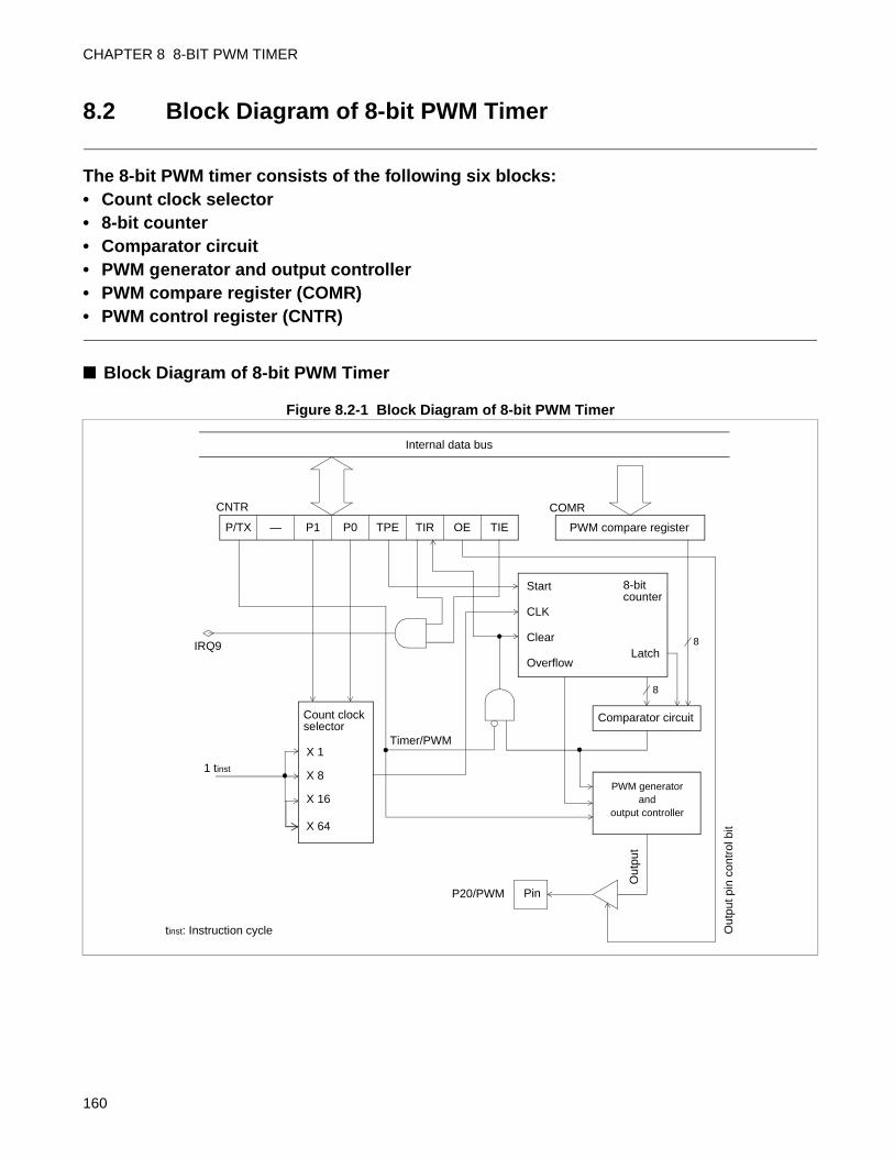
CHAPTER 8 8-BIT PWM TIMER
8.2 Block Diagram of 8-bit PWM Timer
The 8-bit PWM timer consists of the following six blocks:• Count clock selector• 8-bit counter• Comparator circuit• PWM generator and output controller• PWM compare register (COMR)• PWM control register (CNTR)
Block Diagram of 8-bit PWM Timer
Figure 8.2-1 Block Diagram of 8-bit PWM Timer
P/TX — P1 P0 TPE TIR OE TIE
Internal data bus
PWM compare register
IRQ9
Start
CLK
Clear
Overflow
8-bit counter
Latch
Comparator circuitCount clock selector
X 1
X 8
X 16PWM generator
and output controller
Out
put
PinP20/PWM
Out
put p
in c
ontr
ol b
it
1 tinst
Timer/PWM
8
8
tinst: Instruction cycle
CNTR COMR
X 64
160

Count clock selector
Selects a count-up clock for the 8-bit counter from the four internal count clocks.
8-bit counter
The 8-bit counter counts-up on the count clock selected by the count clock selector.
Comparator circuit
The comparator circuit has a latch to hold the COMR register value. The circuit latches the COMR register
value when the 8-bit counter value is "00H". The comparator circuit compares the 8-bit counter value with
the latched COMR register value, and detects when a match occurs.
PWM generator and output controller
When a match is detected during interval timer operation, an interrupt request is generated and, if the
output pin control bit (CNTR: OE) is "1", the output controller inverts the output level of the PWM pin. in
this case, the 8-bit counter is cleared.
When a match is detected during PWM timer operation, the PWM generator changes the output level of the
PWM pin from "H" to "L". The pin is set back to the "H" level when the next overflow occurs on the 8-bit
counter.
PWM compare register (COMR)
The COMR register is used to set the value that is compared with the value of the 8-bit counter.
PWM control register (CNTR)
The CNTR register is used to select the operating mode, enable or disable operation, set the count clock,
control interrupts, and check the PWM status.
Setting the operation to PWM timer mode (P/TX = 0) disables clearing of the 8-bit counter and generation
of interrupt requests IRQ9 when the comparator circuit detects a match.
161
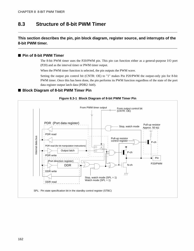
CHAPTER 8 8-BIT PWM TIMER
8.3 Structure of 8-bit PWM Timer
This section describes the pin, pin block diagram, register source, and interrupts of the 8-bit PWM timer.
Pin of 8-bit PWM Timer The 8-bit PWM timer uses the P20/PWM pin. This pin can function either as a general-purpose I/O port
(P20) and as the interval timer or PWM timer output.
When the PWM timer function is selected, the pin outputs the PWM wave.
Setting the output pin control bit (CNTR: OE) to "1" makes Pin P20/PWM the output-only pin for 8-bit
PWM timer. Once this has been done, the pin performs its PWM function regardless of the state of the port
data register output latch data (PDR2: bit0).
Block Diagram of 8-bit PWM Timer Pin
Figure 8.3-1 Block Diagram of 8-bit PWM Timer Pin
PDR (Port data register)
DDR
Inte
rnal
dat
a bu
s
PDR read
PDR read (for bit manipulation instructions)
Output latch
PDR write
DDR write
Pin
SPL: Pin state specification bit in the standby control register (STBC)
N-ch
Stop, watch mode (SPL = 1)
(Port direction register)
From PWM timer output From output control bit(CNTR: OE)
Stop, watch mode
P-ch
Pull-up resistorcontrol register
Pull-up resistorApprox. 50 kΩ
P-ch
DDR read
P20/PWM
Watch mode (SPL = 1)
162
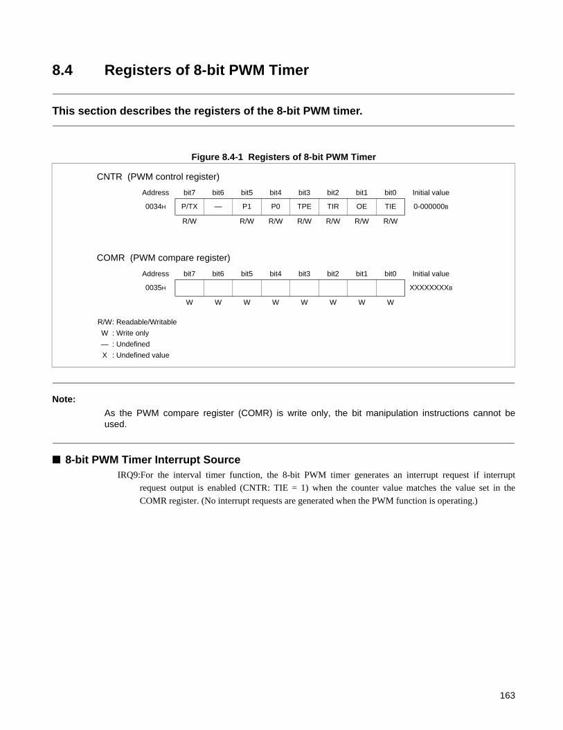
8.4 Registers of 8-bit PWM Timer
This section describes the registers of the 8-bit PWM timer.
Figure 8.4-1 Registers of 8-bit PWM Timer
Note:
As the PWM compare register (COMR) is write only, the bit manipulation instructions cannot beused.
8-bit PWM Timer Interrupt SourceIRQ9:For the interval timer function, the 8-bit PWM timer generates an interrupt request if interrupt
request output is enabled (CNTR: TIE = 1) when the counter value matches the value set in the
COMR register. (No interrupt requests are generated when the PWM function is operating.)
CNTR (PWM control register)
COMR (PWM compare register)
Address bit7 bit6 bit5 bit4 bit3 bit2 bit1 bit0 Initial value
0034H P/TX — P1 P0 TPE TIR OE TIE 0-000000B
R/W R/W R/W R/W R/W R/W R/W
Address bit7 bit6 bit5 bit4 bit3 bit2 bit1 bit0 Initial value
0035H XXXXXXXXB
W W W W W W W W
R/W: Readable/Writable
W : Write only
— : Undefined
X : Undefined value
163
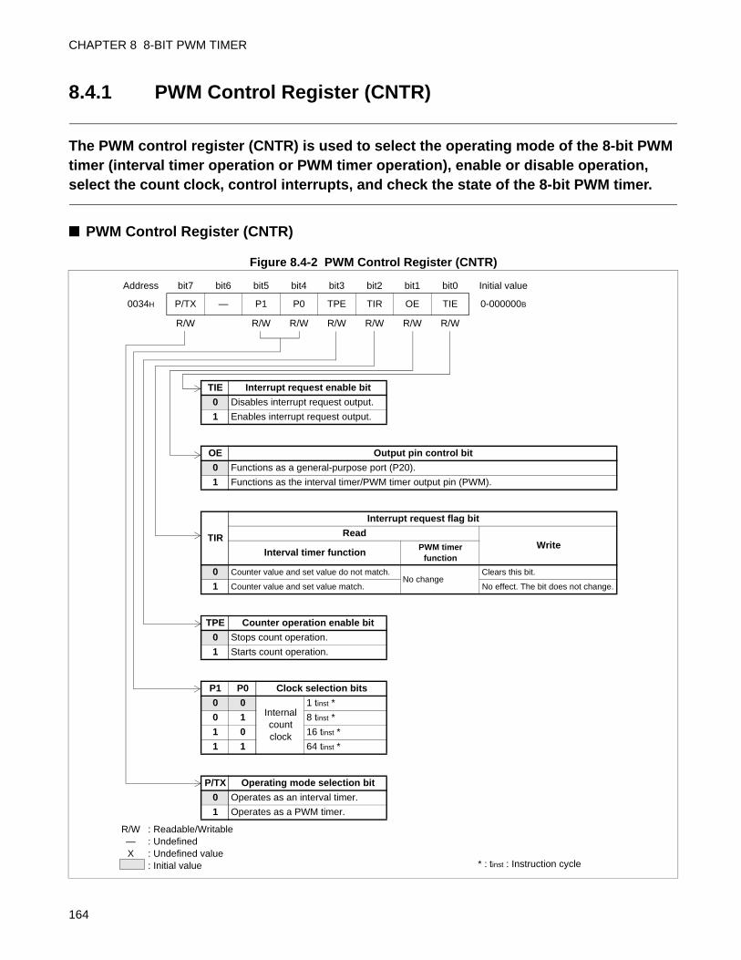
CHAPTER 8 8-BIT PWM TIMER
8.4.1 PWM Control Register (CNTR)
The PWM control register (CNTR) is used to select the operating mode of the 8-bit PWM timer (interval timer operation or PWM timer operation), enable or disable operation, select the count clock, control interrupts, and check the state of the 8-bit PWM timer.
PWM Control Register (CNTR)
Figure 8.4-2 PWM Control Register (CNTR)
Address bit7 bit6 bit5 bit4 bit3 bit2 bit1 bit0 Initial value
0034H P/TX — P1 P0 TPE TIR OE TIE 0-000000B
R/W R/W R/W R/W R/W R/W R/W
TIE Interrupt request enable bit
0 Disables interrupt request output.
1 Enables interrupt request output.
OE Output pin control bit
0 Functions as a general-purpose port (P20).
1 Functions as the interval timer/PWM timer output pin (PWM).
TIR
Interrupt request flag bit
ReadWrite
Interval timer function PWM timer function
0 Counter value and set value do not match.No change
Clears this bit.
1 Counter value and set value match. No effect. The bit does not change.
TPE Counter operation enable bit
0 Stops count operation.
1 Starts count operation.
P1 P0 Clock selection bits
0 0Internal count clock
1 tinst *
0 1 8 tinst *
1 0 16 tinst *
1 1 64 tinst *
P/TX Operating mode selection bit
0 Operates as an interval timer.
1 Operates as a PWM timer.
* : tinst : Instruction cycle
R/W : Readable/Writable— : UndefinedX : Undefined value
: Initial value
164

Table 8.4-1 Functions of Bits in PWM Control Register (CNTR)
Bit name Function
bit7P/TX: Operating mode selection bit
This bit switches between the interval timer function (P/TX = 0) and PWM timer function (P/TX =1). Note:
Write to this bit when the counter operation is stopped (TPE = 0), interrupts are disabled (TIE = 0), and the interrupt request flag bit is cleared (TIR = 0).
bit6 Undefined bitThe read value is undefined. Writing to this bit has no effect on the operation.
bit5,bit4
P1, P0: Clock selection bits
These bits select the count clock for the interval timer function and PWM timer function. These bits can select the count clock from four internal count clocks.Note:
Do not change P1 and P0 when the counter is operating (TPE = 1).
bit3TPE: Counter operation enable bit
This bit activates or stops operation of the PWM timer function and interval timer function. Writing "1" to this bit starts the count operation. Writing "0" to this bit stops the count and clears the counter to "00H".
bit2TIR: Interrupt request flag bit
For the interval timer function: This bit is set to "1" when the counter and PWM compare register (COMR) values match. An interrupt request is output to the CPU when both this bit and the interrupt request enable bit (TIE) are "1".For the PWM timer function: Interrupt requests are not generated.Writing "0" clears this bit. Writing "1" has no effect and does not change the bit value.
bit1OE: Output pin control bit
The P20/PWM pin functions as a general-purpose port (P20) when this bit is set to "0", and a dedicated pin (PWM) when this bit is set to "1". The PWM pin outputs a square wave when the interval timer function is selected and a PWM waveform when the PWM timer function is selected.
bit0TIE: Interrupt request enable bit
This bit enables or disables interrupt request output to the CPU. An interrupt request is output when both this bit and the interrupt request flag bit (TIR) are "1".
165

CHAPTER 8 8-BIT PWM TIMER
8.4.2 PWM Compare Register (COMR)
The PWM compare register (COMR) sets the interval time for the interval timer function.The register value sets the "H" width of the pulse for the PWM timer function.
PWM Compare Register (COMR)Figure 8.4-3 shows the bit structure of the PWM compare register.
As the register is write-only, bit manipulation instructions cannot be used.
Figure 8.4-3 PWM Compare Register (COMR)
Interval timer operation
This register is used to set the value to be compared with the counter value. The register specifies the
interval time.
The counter is cleared when the counter value matches the value set in this register, and the interrupt
request flag bit is set to "1" (CNTR: TIR = 1).
If data is written to the COMR register during counter operation, the new value applies from the next cycle
(after the next match is detected).
Reference:
The COMR setting for interval timer operation can be calculated using the following formula.
The instruction cycle time is affected by the clock mode, and the speed-shift selection.
COMR register value = interval time/(count clock cycle × instruction speed-shifting cycle) - 1
PWM timer operation
This register is used to set the value to be compared with the counter value. The register therefore sets the
"H" width of the pulse.
The PWM pin outputs an "H" level until the counter value matches the value set in this register. From the
match until the counter value overflows, the PWM pin outputs an "L" level.
If data is written to the COMR register during counter operation, the new value applies from the next cycle
(after the next overflow).
Address bit7 bit6 bit5 bit4 bit3 bit2 bit1 bit0 Initial value
0035H XXXXXXXXB
W W W W W W W W
W: Write only
X: Undefined value
166

Note:
In PWM timer operation, the COMR setting and the PWM cycle time can be calculated using thefollowing formulas. The instruction cycle time is affected by the clock mode, and the speed-shiftselection.
COMR register value = duty ratio (%) × 256
PWM wave cycle = count clock cycle × instruction cycle × 256
167
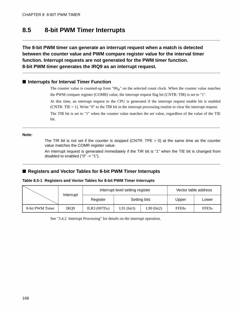
CHAPTER 8 8-BIT PWM TIMER
8.5 8-bit PWM Timer Interrupts
The 8-bit PWM timer can generate an interrupt request when a match is detected between the counter value and PWM compare register value for the interval timer function. Interrupt requests are not generated for the PWM timer function.8-bit PWM timer generates the IRQ9 as an interrupt request.
Interrupts for Interval Timer FunctionThe counter value is counted-up from "00H" on the selected count clock. When the counter value matches
the PWM compare register (COMR) value, the interrupt request flag bit (CNTR: TIR) is set to "1".
At this time, an interrupt request to the CPU is generated if the interrupt request enable bit is enabled
(CNTR: TIE = 1). Write "0" to the TIR bit in the interrupt processing routine to clear the interrupt request.
The TIR bit is set to "1" when the counter value matches the set value, regardless of the value of the TIE
bit.
Note:
The TIR bit is not set if the counter is stopped (CNTR: TPE = 0) at the same time as the countervalue matches the COMR register value.
An interrupt request is generated immediately if the TIR bit is "1" when the TIE bit is changed fromdisabled to enabled ("0" -> "1").
Registers and Vector Tables for 8-bit PWM Timer Interrupts
See "3.4.2 Interrupt Processing" for details on the interrupt operation.
Table 8.5-1 Registers and Vector Tables for 8-bit PWM Timer Interrupts
InterruptInterrupt level setting register Vector table address
Register Setting bits Upper Lower
8-bit PWM Timer IRQ9 ILR3 (007DH) L91 (bit3) L90 (bit2) FFE8H FFE9H
168

8.6 Operation of Interval Timer Function
This section describes the operation of the interval timer function of the 8-bit PWM timer.
Operation of Interval Timer FunctionFigure 8.6-1 shows the settings required to operate as an interval timer function.
Figure 8.6-1 Interval Timer Function Settings
On activation, the counter starts counting-up from "00H" on the rising edge of the selected count clock.
When the counter value matches the value set in the COMR register (compare value), the PWM timer
inverts the level of the PWM pin (PWM) on the next rising edge of the count clock, clears the counter, sets
the interrupt request flag bit (CNTR: TIR = 1), and restarts counting from "00H".
Figure 8.6-2 shows the operation of the 8-bit PWM timer.
Figure 8.6-2 Operation of 8-bit PWM Timer
Do not change the count clock cycle (CNTR: P1, P0) during operation of the interval timer function(CNTR: TPE = 1).
Setting the COMR register value to "00H" causes the PWM pin output to be inverted with the cycle of the
selected count clock.
When the counter is stopped (CNTR: TPE = 0) while the interval timer function is selected, the PWM pinoutputs an "L" level.
bit7 bit6 bit5 bit4 bit3 bit2 bit1 bit0
CNTR P/TX — P1 P0 TPE TIR OE TIE
0 1
COMR Sets interval time (compare value).
: Used bit1 : Set "1".0 : Set "0".
Counter value Compare value (FFH) Compare value (80H)
FFH
80H
00H
COMR value (FFH)
Timer cycle COMR value modified (FFH → 80H)*
Cleared by the program
Time
TIR bit
TPE bit
OE bit
PWM pin
When the output pin control bit (OE) is "0", the pin operates as a general-purpose I/O port (P20).
*: If the PWM compare register (COMR) value is modified during counter operation, the new value is used from the next cycle.
169

CHAPTER 8 8-BIT PWM TIMER
8.7 Operation of PWM Timer Function
This section describes the operation of the PWM timer function of the 8-bit PWM timer.
Operation of PWM Timer FunctionFigure 8.7-1 shows the settings required to operate as the PWM timer function in the 8-bit PWM mode.
Figure 8.7-1 PWM Timer Function Settings
On activation, the counter starts counting-up from "00H" on the rising edge of the selected count clock. The
PWM pin (PWM waveform) outputs an "H" level until the counter value matches the value set in the
COMR register. From the match until the counter value overflows (FFH -> 00H), the PWM pin outputs an
"L" level.
Figure 8.7-2 shows the PWM waveforms output from the PWM pin.
Figure 8.7-2 Example of PWM Waveform Output (PWM Pin)
Notes:
• Do not change the count clock cycle (CNTR: P1, P0) during operation of the PWM timer function(CNTR: TPE = 1).
• When the PWM timer function is selected, the PWM pin maintains its existing level when thecounter is stopped (CNTR: TPE = 0).
bit7 bit6 bit5 bit4 bit3 bit2 bit1 bit0
CNTR P/TX — P1 P0 TPE TIR OE TIE
1 1 × 1 ×
COMR Sets “H” width of pulse (compare value).
: Used bit× : Unused bit 1 : Set "1".
For COMR register value of "00H" (duty ratio = 0%)
Counter value 00H
H
L
H
L
H
L
00H
00H
Counter value
Counter value
PWM waveform
PWM waveform
PWM waveform
For COMR register value of "80H" (duty ratio = 50%)
For COMR register value of "FFH" (duty ratio = 99.6%)
FFH00H
FFH00H
FFH00H
80H
One count width
170
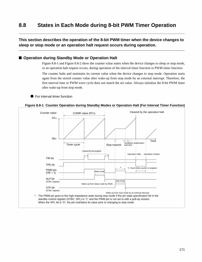
8.8 States in Each Mode during 8-bit PWM Timer Operation
This section describes the operation of the 8-bit PWM timer when the device changes to sleep or stop mode or an operation halt request occurs during operation.
Operation during Standby Mode or Operation HaltFigure 8.8-1 and Figure 8.8-2 show the counter value states when the device changes to sleep or stop mode,
or an operation halt request occurs, during operation of the interval timer function or PWM timer function.
The counter halts and maintains its current value when the device changes to stop mode. Operation starts
again from the stored counter value after wake-up from stop mode by an external interrupt. Therefore, the
first interval time or PWM wave cycle does not match the set value. Always initialize the 8-bit PWM timer
after wake-up from stop mode.
For interval timer function
Figure 8.8-1 Counter Operation during Standby Modes or Operation Halt (For Interval Timer Function)
Counter value COMR value (FFH)
FFH
00H
Timer cycleTime
TIR bit
TPE bit
PWM pin
SLP bit
Cleared by the program
Stop requestOscillation stabilization wait time
Cleared by the operation halt.
Operation halts Operation restarts
(OE = 1)
(STBC register)
STP bit (STBC register)
Sleep mode
Wake-up from sleep mode by IRQ9.
"L" level while counter is stopped.*
Stop mode
Wake-up from stop mode by an external interrupt.
* : The PWM pin goes to the high-impedance state during stop mode if the pin state specification bit in the standby control register (STBC: SPL) is "1" and the PWM pin is not set to with a pull-up resistor. When the SPL bit is "0", the pin maintains its value prior to changing to stop mode.
171
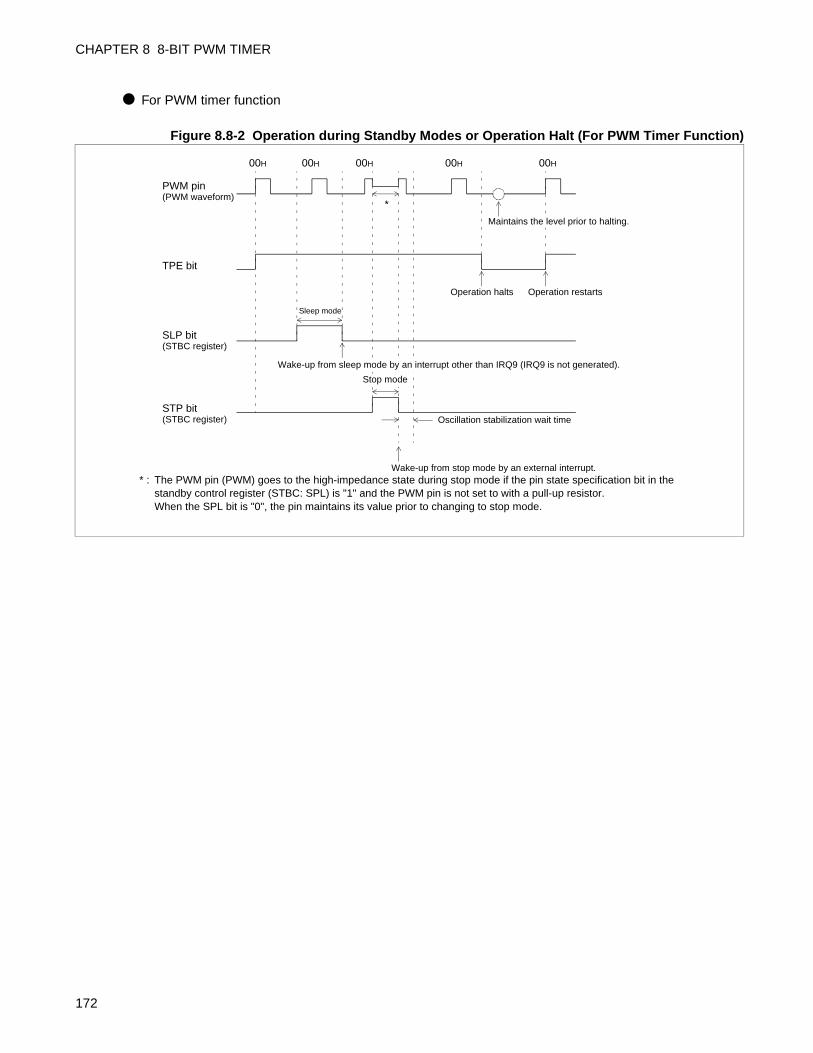
CHAPTER 8 8-BIT PWM TIMER
For PWM timer function
Figure 8.8-2 Operation during Standby Modes or Operation Halt (For PWM Timer Function)
*
PWM pin (PWM waveform)
TPE bit
SLP bit (STBC register)
STP bit (STBC register)
Sleep mode
Wake-up from sleep mode by an interrupt other than IRQ9 (IRQ9 is not generated).
Operation halts
Maintains the level prior to halting.
Operation restarts
Oscillation stabilization wait time
Wake-up from stop mode by an external interrupt.* : The PWM pin (PWM) goes to the high-impedance state during stop mode if the pin state specification bit in the
standby control register (STBC: SPL) is "1" and the PWM pin is not set to with a pull-up resistor.When the SPL bit is "0", the pin maintains its value prior to changing to stop mode.
00H 00H 00H 00H 00H
Stop mode
172

8.9 Notes on Using 8-bit PWM Timer
This section lists points to note when using the 8-bit PWM Timer.
Notes on Using 8-bit PWM Timer
Error
Activating the counter by program is not synchronized with the start of counting-up using the selected
count clock. Therefore, the time from activating the counter until a match with the PWM compare register
(COMR) is detected may be shorter than the theoretical time by a maximum of one cycle of the count
clock. Figure 8.9-1 shows the error that occurs on starting counter operation.
Figure 8.9-1 Error on Starting Counter Operation
Notes on setting by program
• Do not change the count clock cycle (CNTR: P1, P0) when the interval timer function or PWM timer
function is operating (CNTR: TPE = 1).
• Stop the counter (CNTR: TPE = 0), disable interrupts (TIE = 0), and clear the interrupt request flag
(TIR = 0) before switching between the interval timer function and PWM timer function (CNTR: P/TX).
• Interrupt processing cannot return if the interrupt request flag bit (CNTR: TIR) is "1" and the interrupt
request enable bit is enabled (CNTR: TIE = 1). Always clear the TIR bit.
• The TIR bit is not set if the counter is disabled (CNTR: TPE = 0) at the same time as the counter and
COMR register values match.
Counter value
Count clock
One cycle
Error Cycle for 00H
Counter activate
00H 01H 02H 03H 04H
173

CHAPTER 8 8-BIT PWM TIMER
8.10 Program Example for 8-bit PWM Timer
This section gives program examples for the 8-bit PWM Timer.
Program Example for Interval Timer Function
Processing description
• Generates repeated interval timer interrupts at 5 ms intervals.
• Outputs a square wave to the PWM pin that inverts after each interval time.
• With a main clock master oscillation FCH of 12.5 MHz, and the highest speed clock selected by the
speed-shift function (1 instruction cycle time = 4/FCH), the COMR register is set for an interval time of
approximately 5 ms. (An internal clock period of 64 tinst is selected as the count clock.) The COMR
register setting is calculated as follows:
COMR register value = 5 ms/(64 × 4/12.5 MHz) - 1 = 243.0 (0F3H)
174

Coding example
Program Example for PWM Timer Function
Processing description
• Generates a PWM wave with a duty ratio of 50%. Then, changes the duty ratio to 25%.
• Does not generate interrupts.
• For a 12.5 MHz source oscillation, (FCH), and the highest speed clock selected by the speed-shift
function (1 instruction cycle time = 4/FCH), selecting the interval 16 tinst count clock gives a PWM wave
cycle of 16 × 4/12.5 MHz × 256 = 1.31 ms.
• The following shows the COMR register value required for a duty ratio of 50%:
COMR register value = 50/100 × 256 = 128 (080H)
CNTR EQU 0034H ; Address of the PWM control registerCOMR EQU 0035H ; Address of the PWM compare register
TPE EQU CNTR:3 ; Define the counter operation enable bit.TIR EQU CNTR:2 ; Define the interrupt request flag bit.
ILR3 EQU 007DH ; Address of the interrupt level setting register 3
INT_V DSEG ABS ; [DATA SEGMENT]ORG 0FFE8H
IRQ9 DW WARI ; Set interrupt vector.INT_V ENDS;-----Main program---------------------------------------------------------------------------------------------------------------------------------------
CSEG ; [CODE SEGMENT]; Stack pointer (SP) etc. are already initialized.
:CLRI ; Disable interrupts.CLRB TPE ; Stop counter operation.MOV ILR3,#11110111B ; Set interrupt level (level 1).MOV COMR,#0F3H ; Value compared with the counter value (interval time)MOV CNTR,#00111011B ; Operate interval timer, select 64 tinst,
start counter operation, clear interrupt request flag, enable PWM pin output, enable interrupt request output.
SETI ; Enable interrupts.:
;-----Interrupt program----------------------------------------------------------------------------------------------------------------------------------WARI CLRB TIR ; Clear interrupt request flag.
PUSHW AXCHW A,T ; Save A and T.PUSHW A
:User processing
:POPW AXCHW A,T ; Restore A and T.POPW ARETIENDS
;--------------------------------------------------------------------------------------------------------------------------------------------------------------END
175
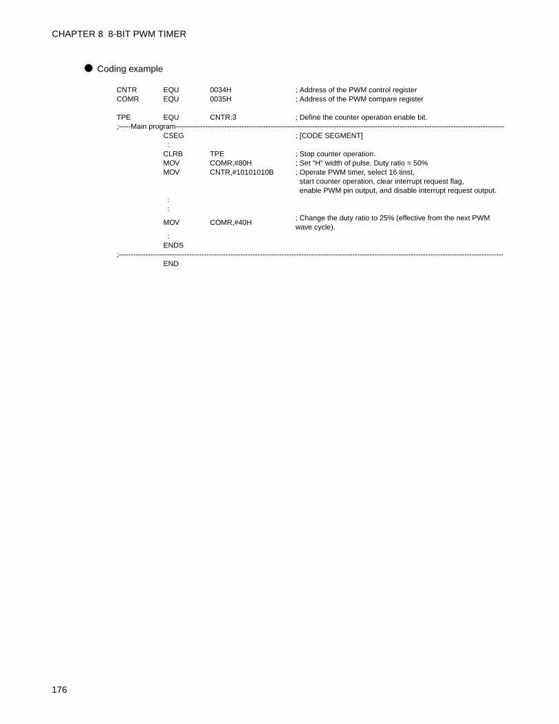
CHAPTER 8 8-BIT PWM TIMER
Coding example
CNTR EQU 0034H ; Address of the PWM control registerCOMR EQU 0035H ; Address of the PWM compare register
TPE EQU CNTR:3 ; Define the counter operation enable bit.;-----Main program---------------------------------------------------------------------------------------------------------------------------------------
CSEG ; [CODE SEGMENT]:
CLRB TPE ; Stop counter operation.MOV COMR,#80H ; Set "H" width of pulse. Duty ratio = 50%MOV CNTR,#10101010B ; Operate PWM timer, select 16 tinst,
start counter operation, clear interrupt request flag, enable PWM pin output, and disable interrupt request output.
::
MOV COMR,#40H; Change the duty ratio to 25% (effective from the next PWM wave cycle).
:ENDS
;--------------------------------------------------------------------------------------------------------------------------------------------------------------END
176
CHAPTER 9PWC TIMER
This chapter describes the functions and operation of the PWC Timer (pulse width count timer).
9.1 Overview of Pulse Width Count Timer
9.2 Block Diagram of Pulse Width Count Timer
9.3 Structure of Pulse Width Count Timer
9.4 Registers of Pulse Width Count Timer
9.5 Pulse Width Count Timer Interrupts
9.6 Operation of Interval Timer Function
9.7 Operation of Pulse Width Measurement Function
9.8 States in Each Mode during Pulse Width Count Timer Operation
9.9 Notes on Using Pulse Width Count Timer
9.9 Notes on Using Pulse Width Count Timer
9.10 Program Example for Timer Function of Pulse Width Count Timer
9.11 Program Example for Pulse Width Measurement Function of Pulse Width Count Timer
177
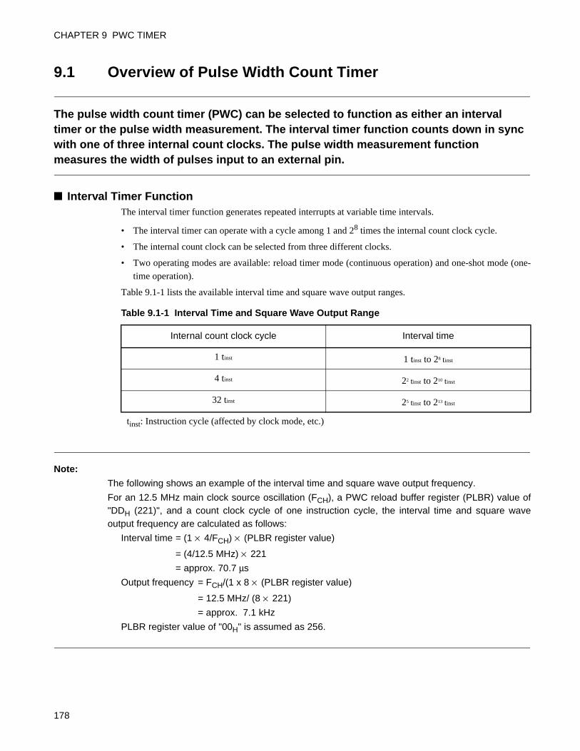
CHAPTER 9 PWC TIMER
9.1 Overview of Pulse Width Count Timer
The pulse width count timer (PWC) can be selected to function as either an interval timer or the pulse width measurement. The interval timer function counts down in sync with one of three internal count clocks. The pulse width measurement function measures the width of pulses input to an external pin.
Interval Timer FunctionThe interval timer function generates repeated interrupts at variable time intervals.
• The interval timer can operate with a cycle among 1 and 28 times the internal count clock cycle.
• The internal count clock can be selected from three different clocks.
• Two operating modes are available: reload timer mode (continuous operation) and one-shot mode (one-
time operation).
Table 9.1-1 lists the available interval time and square wave output ranges.
Note:
The following shows an example of the interval time and square wave output frequency.
For an 12.5 MHz main clock source oscillation (FCH), a PWC reload buffer register (PLBR) value of"DDH (221)", and a count clock cycle of one instruction cycle, the interval time and square waveoutput frequency are calculated as follows:
Interval time = (1 × 4/FCH) × (PLBR register value)
= (4/12.5 MHz) × 221
= approx. 70.7 µs
Output frequency = FCH/(1 x 8 × (PLBR register value)
= 12.5 MHz/ (8 × 221)
= approx. 7.1 kHz
PLBR register value of "00H" is assumed as 256.
Table 9.1-1 Interval Time and Square Wave Output Range
Internal count clock cycle Interval time
1 tinst 1 tinst to 28 tinst
4 tinst 22 tinst to 210 tinst
32 tinst 25 tinst to 213 tinst
tinst: Instruction cycle (affected by clock mode, etc.)
178

Pulse Width Measurement FunctionThe pulse width measurement function can measure the "H" width, "L" width, and one-cycle width of
pulses input to an external pin (PWC pin).
• The PWC can perform continuous pulse width measurement.
• The measurement speed (internal count clock) can be selected from three different speeds.
• The width of long input pulses can be measured using an interrupt processing routine.
Table 9.1-2 lists the available pulse widths measured by the pulse width measurement function.
Table 9.1-2 Pulse Width Measured by Pulse Width Measurement Function
Internal count clock cycle Interval time
1 tinst 1 tinst to 28 tinst
4 tinst 22 tinst to 210 tinst
32 tinst 25 tinst to 213 tinst
tinst: Instruction cycle (affected by clock mode, etc.)
179
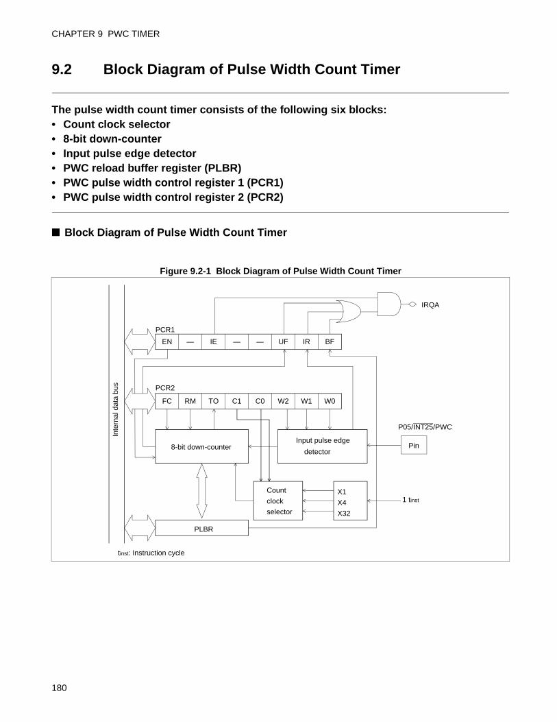
CHAPTER 9 PWC TIMER
9.2 Block Diagram of Pulse Width Count Timer
The pulse width count timer consists of the following six blocks:• Count clock selector• 8-bit down-counter• Input pulse edge detector• PWC reload buffer register (PLBR)• PWC pulse width control register 1 (PCR1)• PWC pulse width control register 2 (PCR2)
Block Diagram of Pulse Width Count Timer
Figure 9.2-1 Block Diagram of Pulse Width Count Timer
FC RM TO C1 C0 W2 W1 W0
IRQA
PLBR
X1
X4
X32
EN — IE — — UF IR BF
1 tinst
Inte
rnal
dat
a bu
s
8-bit down-counterInput pulse edge
detector
Count
clock
selector
tinst: Instruction cycle
PCR1
PCR2
Pin
P05/INT25/PWC
180
Count clock selector
Selects a count-down clock for the 8-bit down-counter from the three available internal count clocks.
8-bit down-counter
The 8-bit down-counter starts counting from the value set in the PWC reload buffer register (PLBR) when
operating as an interval timer, and from FFH when performing pulse width measurement. When an
underflow (00H -> FFH) occurs, the counter inverts the timer output bit (PCR2: TO).
Input pulse edge detector
Operates when the pulse width measurement function is selected, and starts or stops the 8-bit down-counter
when an edge input from the PWC pin matches the edge specified by the PWC pulse width control register
2 (PCR2).
PWC reload buffer register (PLBR)
When operating in reload timer mode of the interval timer function, the PLBR register value is re-loaded to
the counter and the count continues whenever a counter value underflow (00H -> FFH) occurs.
When performing pulse width measurement, the value of the 8-bit down-counter is transferred to the PLBR
register when measurement completes.
PWC pulse width control register1, 2 (PCR1, PCR2)
These registers are used to select the function, set operating conditions, enable or disable operation, control
interrupts, and to check the PWC status.
181

CHAPTER 9 PWC TIMER
9.3 Structure of Pulse Width Count Timer
This section describes the pins, pin block diagram, registers, and interrupt source of the pulse width count timer.
Pins of Pulse Width Count TimerThe pulse width count timer uses the P05/INT25/PWC pin, which can function either as general-purpose
I/O port (P05), or as the measured pulse input (PWC), and external interrupt input (INT25).
PWC:The pulse width measurement function measures the pulse widths input to this pin.
Set the pin as an input port in the port direction register (DDR0: bit5 = 0) when using as the PWC pin for
the pulse width measurement function.
Block Diagram of Pulse Width Count Timer Pins
Figure 9.3-1 Block Diagram of Pulse Width Count Timer Pins
Reference:
When pull-up resistor is selected in pull-up resistor control register, the states of these pins in stopmode (SPL=1) are in "H" level (pull-up state) rather than high impedance. However, during reset,pull-up is unavailable and will be in high impedance state.
PDR (Port data register)
DDR
Inte
rnal
dat
a bu
s
PDR read
PDR read (for bit manipulation instructions)
PDR write
DDR write (Port direction register)
Pull-up resistorApprox. 50 kΩ
Pin
SPL: Pin state specification bit in the standby control register (STBC)
N-ch
P-ch
P-ch
Stop, watch mode
Stop, watch mode
Pull-up resistorcontrol register
Output latch
To PWC Timer input
P05/INT25/PWC
(SPL = 1)
182
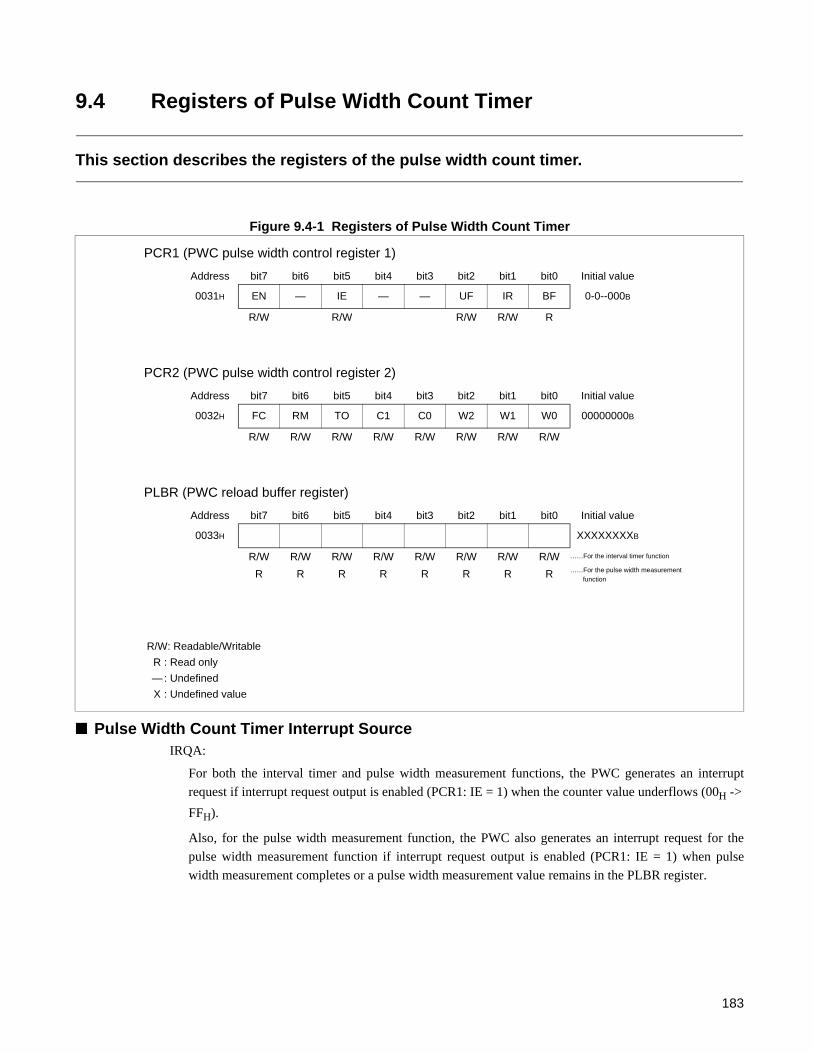
9.4 Registers of Pulse Width Count Timer
This section describes the registers of the pulse width count timer.
Figure 9.4-1 Registers of Pulse Width Count Timer
Pulse Width Count Timer Interrupt SourceIRQA:
For both the interval timer and pulse width measurement functions, the PWC generates an interrupt
request if interrupt request output is enabled (PCR1: IE = 1) when the counter value underflows (00H ->
FFH).
Also, for the pulse width measurement function, the PWC also generates an interrupt request for the
pulse width measurement function if interrupt request output is enabled (PCR1: IE = 1) when pulse
width measurement completes or a pulse width measurement value remains in the PLBR register.
PCR1 (PWC pulse width control register 1)
PCR2 (PWC pulse width control register 2)
PLBR (PWC reload buffer register)
Address bit7 bit6 bit5 bit4 bit3 bit2 bit1 bit0 Initial value
0031H EN — IE — — UF IR BF 0-0--000B
R/W R/W R/W R/W R
Address bit7 bit6 bit5 bit4 bit3 bit2 bit1 bit0 Initial value
0032H FC RM TO C1 C0 W2 W1 W0 00000000B
R/W R/W R/W R/W R/W R/W R/W R/W
Address bit7 bit6 bit5 bit4 bit3 bit2 bit1 bit0 Initial value
0033H XXXXXXXXB
R/W R/W R/W R/W R/W R/W R/W R/W ……For the interval timer function
R R R R R R R R ……For the pulse width measurement function
R/W: Readable/Writable
R : Read only
— : Undefined
X : Undefined value
183
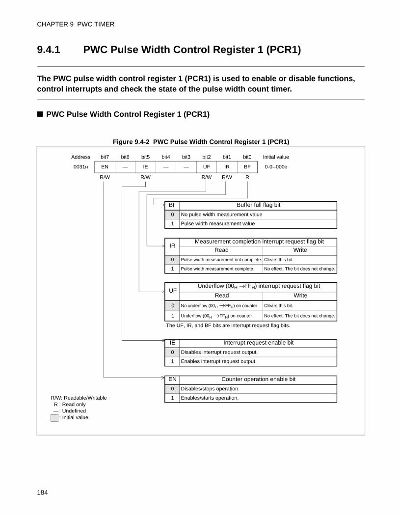
CHAPTER 9 PWC TIMER
9.4.1 PWC Pulse Width Control Register 1 (PCR1)
The PWC pulse width control register 1 (PCR1) is used to enable or disable functions, control interrupts and check the state of the pulse width count timer.
PWC Pulse Width Control Register 1 (PCR1)
Figure 9.4-2 PWC Pulse Width Control Register 1 (PCR1)
Address bit7 bit6 bit5 bit4 bit3 bit2 bit1 bit0 Initial value
0031H EN — IE — — UF IR BF 0-0--000B
R/W R/W R/W R/W R
BF Buffer full flag bit
0 No pulse width measurement value
1 Pulse width measurement value
IR Measurement completion interrupt request flag bit
Read Write
0 Pulse width measurement not complete. Clears this bit.
1 Pulse width measurement complete. No effect. The bit does not change.
UFUnderflow (00H → FFH) interrupt request flag bit
Read Write
0 No underflow (00H → FFH) on counter Clears this bit.
1 Underflow (00H → FFH) on counter No effect. The bit does not change.
The UF, IR, and BF bits are interrupt request flag bits.
IE Interrupt request enable bit
0 Disables interrupt request output.
1 Enables interrupt request output.
EN Counter operation enable bit
0 Disables/stops operation.
1 Enables/starts operation.R/W: Readable/WritableR : Read only— : Undefined
: Initial value
184
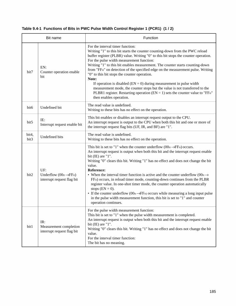
Table 9.4-1 Functions of Bits in PWC Pulse Width Control Register 1 (PCR1) (1 / 2)
Bit name Function
bit7EN: Counter operation enable bit
For the interval timer function: Writing "1" to this bit starts the counter counting-down from the PWC reload buffer register (PLBR) value. Writing "0" to this bit stops the counter operation. For the pulse width measurement function: Writing "1" to this bit enables measurement. The counter starts counting-down from "FFH" on detection of the specified edge on the measurement pulse. Writing "0" to this bit stops the counter operation. Note:
If operation is disabled (EN = 0) during measurement in pulse width measurement mode, the counter stops but the value is not transferred to the PLBR1 register. Restarting operation (EN = 1) sets the counter value to "FFH" then enables operation.
bit6 Undefined bitThe read value is undefined. Writing to these bits has no effect on the operation.
bit5IE: Interrupt request enable bit
This bit enables or disables an interrupt request output to the CPU. An interrupt request is output to the CPU when both this bit and one or more of the interrupt request flag bits (UF, IR, and BF) are "1".
bit4,bit3
Undefined bitsThe read value is undefined. Writing to these bits has no effect on the operation.
bit2UF: Underflow (00H → FFH) interrupt request flag bit
This bit is set to "1" when the counter underflow (00H → FFH) occurs. An interrupt request is output when both this bit and the interrupt request enable bit (IE) are "1". Writing "0" clears this bit. Writing "1" has no effect and does not change the bit value. Reference:• When the interval timer function is active and the counter underflow (00H →
FFH) occurs, in reload timer mode, counting-down continues from the PLBR register value. In one-shot timer mode, the counter operation automatically stops (EN = 0).
• If the counter underflow (00H → FFH) occurs while measuring a long input pulse in the pulse width measurement function, this bit is set to "1" and counter operation continues.
bit1IR: Measurement completion interrupt request flag bit
For the pulse width measurement function: This bit is set to "1" when the pulse width measurement is completed. An interrupt request is output when both this bit and the interrupt request enable bit (IE) are "1". Writing "0" clears this bit. Writing "1" has no effect and does not change the bit value. For the interval timer function:The bit has no meaning.
185
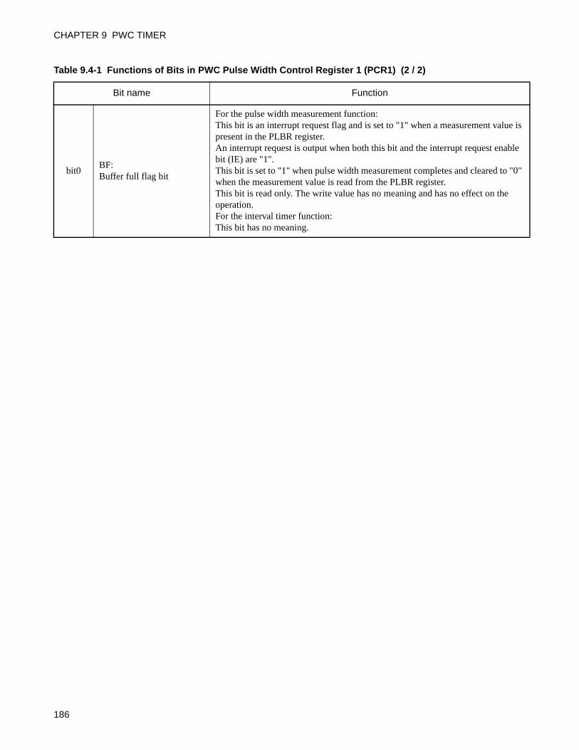
CHAPTER 9 PWC TIMER
bit0BF: Buffer full flag bit
For the pulse width measurement function: This bit is an interrupt request flag and is set to "1" when a measurement value is present in the PLBR register. An interrupt request is output when both this bit and the interrupt request enable bit (IE) are "1". This bit is set to "1" when pulse width measurement completes and cleared to "0" when the measurement value is read from the PLBR register. This bit is read only. The write value has no meaning and has no effect on the operation. For the interval timer function:This bit has no meaning.
Table 9.4-1 Functions of Bits in PWC Pulse Width Control Register 1 (PCR1) (2 / 2)
Bit name Function
186

9.4.2 PWC Pulse Width Control Register 2 (PCR2)
The PWC pulse width control register 2 (PCR2) is used to select the operating mode (pulse width measurement or interval timer operation, etc.), select the count clock, set the measured pulse (measurement edges), and check the timer output state of the pulse width count timer.
PWC Pulse Width Control Register 2 (PCR2)
Figure 9.4-3 PWC Pulse Width Control Register 2 (PCR2)
Address bit7 bit6 bit5 bit4 bit3 bit2 bit1 bit0 Initial value
0032H FC RM TO C1 C0 W2 W1 W0 00000000B
R/W R/W R/W R/W R/W R/W R/W R/W
W2 W1 W0 Measured pulse selection bitsOnly applies to the pulse width measurement function (FC = 1)
0 0 0 "H" pulse (rising edge to falling edge)
0 0 1 "L" pulse (falling edge to rising edge)
0 1 0 Rising edge to rising edge (one cycle)
0 1 1 Falling edge to falling edge (one cycle)
1 1 0 Both edges
C1 C0 Count clock selection bits
0 0 1 tinst
0 1 4 tinst
1 0 32 tinst
1 1 Do not use this setting
tinst: Instruction cycle
TOTimer output bit
Read Write
0 Reads the current output value.
Can be used to set the output value when the counter is stopped.1
RMReload mode selection bit
Only applies to the interval timer function (FC = 0).
0 Reload timer mode
1 One-shot timer mode
FC Operating mode selection bit
0 Operates as an interval timer function.
1 Operates as a pulse width measurement function.R/W: Readable/Writable
: Initial value
187

CHAPTER 9 PWC TIMER
Note:
Do not modify the PCR2 register while the counter is operating (PCR1: EN = 1).
Table 9.4-2 Functions of Bits in PWC Pulse Width Control Register 2 (PCR2)
Bit name Function
bit7FC: Operating mode selection bit
This bit switches between the interval timer function (FC = 0) and pulse width measurement function (FC = 1). Note:
When using the pulse width measurement function (FC = 1), set the P05/INT25/PWC pin as an input port.
bit6RM: Reload mode selection bit
For the interval timer function: This bit selects reload timer mode (RM = 0) or one-shot timer mode (RM = 1). For the pulse width measurement function: This bit has no meaning.
bit5TO: Timer output bit
The value of this bit is inverted each time a counter value underflow (00H → FFH) occurs. By counting the number of times this bit is inverted (number of underflow (00H → FFH)
occurs), pulse widths longer than 28 × the cycle of the selected count clock can be
measured.
bit4,bit3
C1, C0: Count clock selection bits
These bits select the count clock for the interval timer function and pulse width measurement function. Three internal count clocks can be selected.
bit2to
bit0
W2, W1, W0: Measured pulse selection bits
For the pulse width measurement function: These bits select which pulse edges to use as the start and end conditions for pulse measurement. Five types of pulse width or cycle can be selected. For the interval timer function: These bits have no meaning.
188

9.4.3 PWC Reload Buffer Register (PLBR)
The PWC reload buffer register (PLBR) functions as a reload register for the interval timer function and as a measurement value storage register for the pulse width measurement function.
PWC Reload Buffer Register (PLBR) Figure 9.4-4 shows the bit configuration of the PWC reload buffer register.
Figure 9.4-4 PWC Reload Buffer Register (PLBR)
For interval timer function
The register functions as a reload register, specifying the interval time.
The counter starts counting-down from the set value written in this register when counter operation is
enabled (PCR1: EN = 1).
In reload timer mode, the PLBR register value is reloaded to the counter and the counter continues
counting-down when a counter value underflows (00H -> FFH). If a value is written to the PLBR register
during counter operation, the new value applies from the next time the counter is reloaded due to an
underflow (00H -> FFH).
Note:
The setting value of the PLBR register for the interval timer function is calculated as follows:
PLBR register value = interval time/(count clock cycle × instruction cycle)
For pulse width measurement function
The register is used to store the pulse width measurement value.
The counter value is transferred to this register when pulse width measurement completes on detection ofthe edge specified for measurement completion.
At this time, the buffer full flag bit (PCR1: BF) and the measurement completion interrupt request flag bit(PCR1: IR) are set to "1". Reading this register clears the BF bit to "0".
The register is read-only for the pulse width measurement function.
Address bit7 bit6 bit5 bit4 bit3 bit2 bit1 bit0 Initial value
0033H XXXXXXXXB
R/W R/W R/W R/W R/W R/W R/W R/W ……For the interval timer function
R R R R R R R R ……For the pulse width measurement function
R/W: Readable/Writable
R : Read only
X : Undefined value
189

CHAPTER 9 PWC TIMER
Reference:
The pulse width for the pulse width measurement function is calculated based on the PLBR registervalue as follows:
Pulse width = (256 - PLBR register value) × count clock cycle × instruction cycle
190
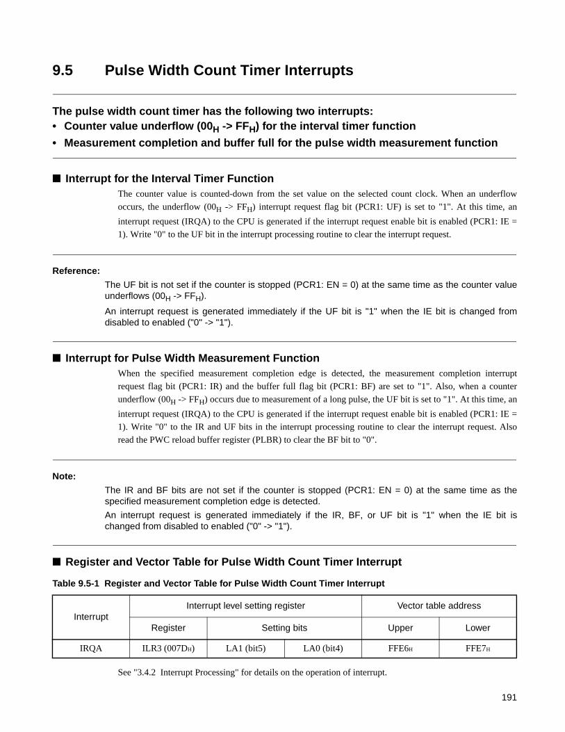
9.5 Pulse Width Count Timer Interrupts
The pulse width count timer has the following two interrupts:• Counter value underflow (00H -> FFH) for the interval timer function
• Measurement completion and buffer full for the pulse width measurement function
Interrupt for the Interval Timer FunctionThe counter value is counted-down from the set value on the selected count clock. When an underflow
occurs, the underflow (00H -> FFH) interrupt request flag bit (PCR1: UF) is set to "1". At this time, an
interrupt request (IRQA) to the CPU is generated if the interrupt request enable bit is enabled (PCR1: IE =
1). Write "0" to the UF bit in the interrupt processing routine to clear the interrupt request.
Reference:
The UF bit is not set if the counter is stopped (PCR1: EN = 0) at the same time as the counter valueunderflows (00H -> FFH).
An interrupt request is generated immediately if the UF bit is "1" when the IE bit is changed fromdisabled to enabled ("0" -> "1").
Interrupt for Pulse Width Measurement FunctionWhen the specified measurement completion edge is detected, the measurement completion interrupt
request flag bit (PCR1: IR) and the buffer full flag bit (PCR1: BF) are set to "1". Also, when a counter
underflow (00H -> FFH) occurs due to measurement of a long pulse, the UF bit is set to "1". At this time, an
interrupt request (IRQA) to the CPU is generated if the interrupt request enable bit is enabled (PCR1: IE =
1). Write "0" to the IR and UF bits in the interrupt processing routine to clear the interrupt request. Also
read the PWC reload buffer register (PLBR) to clear the BF bit to "0".
Note:
The IR and BF bits are not set if the counter is stopped (PCR1: EN = 0) at the same time as thespecified measurement completion edge is detected.
An interrupt request is generated immediately if the IR, BF, or UF bit is "1" when the IE bit ischanged from disabled to enabled ("0" -> "1").
Register and Vector Table for Pulse Width Count Timer Interrupt
See "3.4.2 Interrupt Processing" for details on the operation of interrupt.
Table 9.5-1 Register and Vector Table for Pulse Width Count Timer Interrupt
InterruptInterrupt level setting register Vector table address
Register Setting bits Upper Lower
IRQA ILR3 (007DH) LA1 (bit5) LA0 (bit4) FFE6H FFE7H
191
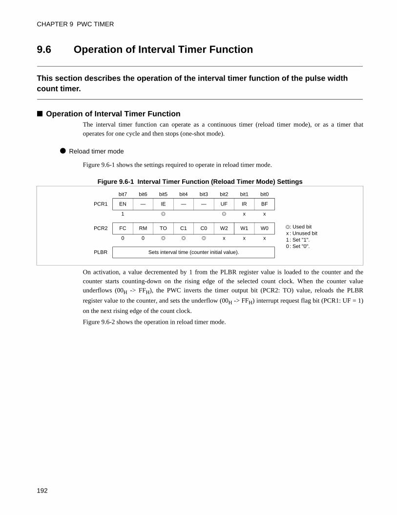
CHAPTER 9 PWC TIMER
9.6 Operation of Interval Timer Function
This section describes the operation of the interval timer function of the pulse width count timer.
Operation of Interval Timer FunctionThe interval timer function can operate as a continuous timer (reload timer mode), or as a timer that
operates for one cycle and then stops (one-shot mode).
Reload timer mode
Figure 9.6-1 shows the settings required to operate in reload timer mode.
Figure 9.6-1 Interval Timer Function (Reload Timer Mode) Settings
On activation, a value decremented by 1 from the PLBR register value is loaded to the counter and the
counter starts counting-down on the rising edge of the selected count clock. When the counter value
underflows (00H -> FFH), the PWC inverts the timer output bit (PCR2: TO) value, reloads the PLBR
register value to the counter, and sets the underflow (00H -> FFH) interrupt request flag bit (PCR1: UF = 1)
on the next rising edge of the count clock.
Figure 9.6-2 shows the operation in reload timer mode.
bit7 bit6 bit5 bit4 bit3 bit2 bit1 bit0
PCR1 EN — IE — — UF IR BF
1 x x
PCR2 FC RM TO C1 C0 W2 W1 W0
0 0 x x x
PLBR Sets interval time (counter initial value).
: Used bitx : Unused bit1 : Set "1".0 : Set "0".
192
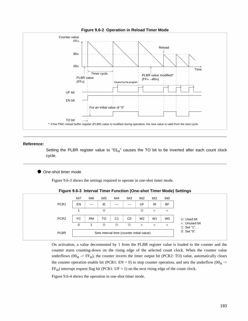
Figure 9.6-2 Operation in Reload Timer Mode
Reference:
Setting the PLBR register value to "01H" causes the TO bit to be inverted after each count clockcycle.
One-shot timer mode
Figure 9.6-3 shows the settings required to operate in one-shot timer mode.
Figure 9.6-3 Interval Timer Function (One-shot Timer Mode) Settings
On activation, a value decremented by 1 from the PLBR register value is loaded to the counter and the
counter starts counting-down on the rising edge of the selected count clock. When the counter value
underflows (00H -> FFH), the counter inverts the timer output bit (PCR2: TO) value, automatically clears
the counter operation enable bit (PCR1: EN = 0) to stop counter operation, and sets the underflow (00H ->
FFH) interrupt request flag bit (PCR1: UF = 1) on the next rising edge of the count clock.
Figure 9.6-4 shows the operation in one-shot timer mode.
Counter valueFFH
80H
00H
Timer cycle
Cleared by the program
Time
UF bit
EN bit
PLBR value (FFH)
PLBR value modified* (FFH → 80H)
Reload
TO bit
For an initial value of "0"
*: If the PWC reload buffer register (PLBR) value is modified during operation, the new value is valid from the next cycle.
bit7 bit6 bit5 bit4 bit3 bit2 bit1 bit0
PCR1 EN — IE — — UF IR BF
1 × ×
PCR2 FC RM TO C1 C0 W2 W1 W0
0 1 × × ×
PLBR Sets interval time (counter initial value).
: Used bit× : Unused bit1 : Set "1".0 : Set "0".
193

CHAPTER 9 PWC TIMER
Figure 9.6-4 Operation in One-shot Timer Mode
Reference:
Do not modify PCR2 when the counter is operating (PCR1: EN = 1).
The UF bit is set to "1" if a counter value underflows (00H -> FFH), regardless of the value of the interrupt
request enable bit (PCR1: IE).
When the counter is stopped (PCR1: EN = 0) while the interval timer function is selected, the TO bit
maintains the value it had immediately before the counter stopped.
Counter value FFH
80H
00H
Timer cycle
Cleared by the program
Time
UF bit
EN bit
PLBR value (FFH)
TO bit
Automatic clear Reactivate
InvertReactivates with the initial value unchanged ("0")
For an initial value of "1" on activation
*: If the PWC reload buffer register (PLBR) value is modified during operation, the new value is used from the next cycle.
Automatic clear Automatic clearReactivate
PLBR value modified (FFH → 80H)*
194
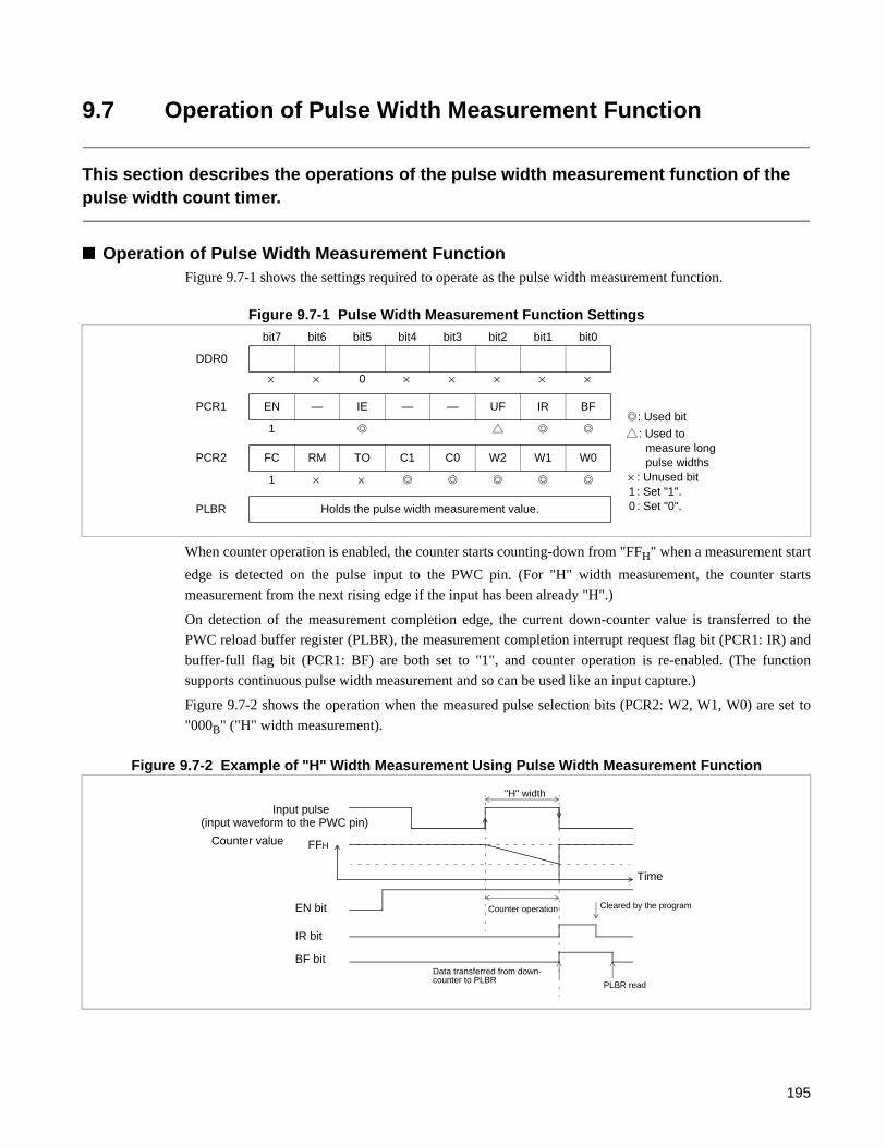
9.7 Operation of Pulse Width Measurement Function
This section describes the operations of the pulse width measurement function of the pulse width count timer.
Operation of Pulse Width Measurement FunctionFigure 9.7-1 shows the settings required to operate as the pulse width measurement function.
Figure 9.7-1 Pulse Width Measurement Function Settings
When counter operation is enabled, the counter starts counting-down from "FFH" when a measurement start
edge is detected on the pulse input to the PWC pin. (For "H" width measurement, the counter starts
measurement from the next rising edge if the input has been already "H".)
On detection of the measurement completion edge, the current down-counter value is transferred to the
PWC reload buffer register (PLBR), the measurement completion interrupt request flag bit (PCR1: IR) and
buffer-full flag bit (PCR1: BF) are both set to "1", and counter operation is re-enabled. (The function
supports continuous pulse width measurement and so can be used like an input capture.)
Figure 9.7-2 shows the operation when the measured pulse selection bits (PCR2: W2, W1, W0) are set to
"000B" ("H" width measurement).
Figure 9.7-2 Example of "H" Width Measurement Using Pulse Width Measurement Function
bit7 bit6 bit5 bit4 bit3 bit2 bit1 bit0
DDR0
× × 0 × × × × ×
PCR1 EN — IE — — UF IR BF
1
PCR2 FC RM TO C1 C0 W2 W1 W0
1 × ×
PLBR Holds the pulse width measurement value.
: Used bit
: Used to measure long pulse widths
× : Unused bit1 : Set "1".0 : Set "0".
Input pulse (input waveform to the PWC pin)
Counter value FFH
EN bit
IR bit
BF bit
"H" width
Counter operation
Time
Cleared by the program
Data transferred from down-counter to PLBR PLBR read
195

CHAPTER 9 PWC TIMER
Notes:
• If the previous PLBR register value has not been read during continuous pulse widthmeasurement, the PWC leaves the BF bit set to "1" and maintains the previous measurementvalue. In this case, the new measurement value is lost.
• Do not modify the PCR1/PCR2 register during pulse width measurement (PCR1: EN = 1).
Measuring Long Pulse Widths
To measure pulse widths longer than 28 times the cycle of the selected count clock, it is necessary to count
the number of counter underflows (00H -> FFH) by software in the interrupt processing routine. Counting
by software requires a buffer in RAM (a software counter) to hold the number of counter underflows (00H ->
FFH).
After initializing the software counter and enabling counter operation, the counter starts counting-down
from "FFH" when a measurement start edge is detected on the pulse input to the PWC pin.
An interrupt request is generated on detection of the measurement completion edge or when the counter
underflows (00H -> FFH). Check the measurement completion interrupt request flag bit (PCR1: IR) and
underflow (00H -> FFH) interrupt request flag bit (PCR1: UF) in the interrupt processing routine. If the UF
bit is "1", write "0" to the UF bit to clear the interrupt request and increment the software counter (the PWC
counter continues to operate).
When the IR bit is "1", calculate the pulse width including underflows (00H -> FFH) from the values of the
software counter and PWC reload buffer register (PLBR).
When the PLBR register value is "00H", calculate as 256.
Calculating the width of long pulses
Pulse width = [(256 - PLBR register value) + (number of counter underflows (00H × FFH) × 256)] × one-
cycle width of count clock
Calculate the pulse width before the next underflow (00H x FFH) occurs. The correct measurement value
may not be able to be calculated after the next underflow (00H x FFH) occurs.
Figure 9.7-3 shows the operation when the measured pulse selection bits (PCR2: W2, W1, W0) are set to
"011B" (falling edge to falling edge).
196

Figure 9.7-3 Measuring Long Pulse Widths
Input pulse (input waveform to the PWC pin)
EN bitFFH
Software counter value
Counter value
UF bit
IR bit
BF bit
Set "0"
One cycle
Cleared by the programCleared by the program
Data transferred from down-counter to PLBR
PLBR read
0 1 2 3
197
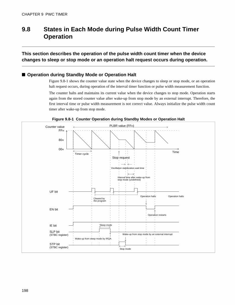
CHAPTER 9 PWC TIMER
9.8 States in Each Mode during Pulse Width Count Timer Operation
This section describes the operation of the pulse width count timer when the device changes to sleep or stop mode or an operation halt request occurs during operation.
Operation during Standby Mode or Operation HaltFigure 9.8-1 shows the counter value state when the device changes to sleep or stop mode, or an operation
halt request occurs, during operation of the interval timer function or pulse width measurement function.
The counter halts and maintains its current value when the device changes to stop mode. Operation starts
again from the stored counter value after wake-up from stop mode by an external interrupt. Therefore, the
first interval time or pulse width measurement is not correct value. Always initialize the pulse width count
timer after wake-up from stop mode.
Figure 9.8-1 Counter Operation during Standby Modes or Operation Halt
Counter valueFFH
80H
00H
PLBR value (FFH)
Timer cycleStop request
Oscillation stabilization wait time
Interval time after wake-up from stop mode (undefined)
Time
UF bit
Cleared by the program
Operation halts
Operation restarts
Operation halts
EN bit
IE bit
SLP bit (STBC register)
STP bit(STBC register)
Wake-up from stop mode by an external interrupt
Wake-up from sleep mode by IRQA
Stop mode
Sleep mode
198
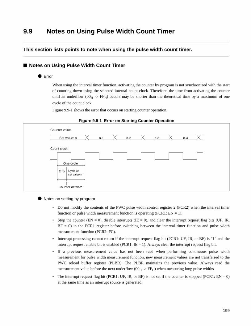
9.9 Notes on Using Pulse Width Count Timer
This section lists points to note when using the pulse width count timer.
Notes on Using Pulse Width Count Timer
Error
When using the interval timer function, activating the counter by program is not synchronized with the start
of counting-down using the selected internal count clock. Therefore, the time from activating the counter
until an underflow (00H -> FFH) occurs may be shorter than the theoretical time by a maximum of one
cycle of the count clock.
Figure 9.9-1 shows the error that occurs on starting counter operation.
Figure 9.9-1 Error on Starting Counter Operation
Notes on setting by program
• Do not modify the contents of the PWC pulse width control register 2 (PCR2) when the interval timer
function or pulse width measurement function is operating (PCR1: EN = 1).
• Stop the counter (EN = 0), disable interrupts (IE = 0), and clear the interrupt request flag bits (UF, IR,
BF = 0) in the PCR1 register before switching between the interval timer function and pulse width
measurement function (PCR2: FC).
• Interrupt processing cannot return if the interrupt request flag bit (PCR1: UF, IR, or BF) is "1" and the
interrupt request enable bit is enabled (PCR1: IE = 1). Always clear the interrupt request flag bit.
• If a previous measurement value has not been read when performing continuous pulse width
measurement for pulse width measurement function, new measurement values are not transferred to the
PWC reload buffer register (PLBR). The PLBR maintains the previous value. Always read the
measurement value before the next underflow (00H -> FFH) when measuring long pulse widths.
• The interrupt request flag bit (PCR1: UF, IR, or BF) is not set if the counter is stopped (PCR1: EN = 0)
at the same time as an interrupt source is generated.
Counter value
Set value: n n-1 n-2 n-3 n-4
Count clock
One cycle
Error Cycle of set value n
Counter activate
199
CHAPTER 9 PWC TIMER
9.10 Program Example for Timer Function of Pulse Width Count Timer
This section gives two program examples for the timer function of the pulse width count timer.
Program Example 1 for Interval Timer Function (Reload Timer Mode)
Processing description
• Generates repeated interval timer interrupts at 3 ms intervals (reload timer mode).
• Outputs a square wave to the TO pin that inverts after each interval time cycle. The initial value of TO
pin is "L" level.
• The following shows the PLBR register value that results in an interval time of approximately 3 ms for a
12.5 MHz source oscillation. The count clock is 32 tinst (tinst: divide-by-four main clock source
oscillation when the highest main clock speed is selected).
PLBR register value = 3 ms/(32 × 4/12.5 MHz) = 293.0 (125H)
200

Coding example
Program Example 2 for Interval Timer Function (One-shot Timer Mode)
Processing description
• Generates a single 3 ms interval timer interrupt (one-shot timer mode).
• Outputs a pulse wave to the TO pin that inverts after each interval time cycle. The initial value of TO
pin is "H" level.
• The following shows the PLBR register value that results in an interval time of approximately 3 ms for a
12.5 MHz source oscillation. The count clock is 32 tinst (tinst: divide-by-four main clock source
oscillation when the highest main clock speed is selected).
PLBR register value = 3 ms/(32 × 4/12.5 MHz) = 293.0 (125H)
PCR1 EQU 0031H ; Address of the PWC pulse width control register 1PCR2 EQU 0032H ; Address of the PWC pulse width control register 2PLBR EQU 0033H ; Address of the PWC reload buffer register
EN EQU PCR1:7 ; Define the counter operation enable bit.IE EQU PCR1:5 ; Define the interrupt request enable bit.UF EQU PCR1:2 ; Define the underflow (00H → FFH) interrupt request flag bit.
ILR3 EQU 007DH ; Address of the interrupt level setting register 3
INT_V DSEG ABS ; [DATA SEGMENT]ORG 0FFE6H
IRQA DW WARI ; Set interrupt vector.INT_V ENDS;-----Main program--------------------------------------------------------------------------------------------------------------------------------------------------------------
CSEG ; [CODE SEGMENT]; Stack pointer (SP) etc. are already initialized.
:CLRI ; Disable interrupts.CLRB EN ; Stop counter operation.CLRB IE ; Disable interrupt request output.MOV ILR3,#11011111B ; Set interrupt level (level 1).MOV PLBR,#125H ; Counter reload value (interval time)MOV PCR2,#00010000B ; Select interval timer function, reload timer mode,
initial output value of the TO bit, and 32 tinst.MOV PCR1,#11100000B ; Start counter operation,
enable interrupt request output, clear underflow (00H → FFH) interrupt request flag, clear measurement completion interrupt request flag (bit 1).
SETI ; Enable interrupts.:
;-----Interrupt processing routine--------------------------------------------------------------------------------------------------------------------------------------------WARI CLRB UF ; Clear interrupt request flag.
PUSHW AXCHW A,TPUSHW A
:User processing
:POPW AXCHW A,TPOPW ARETIENDS
;-------------------------------------------------------------------------------------------------------------------------------------------------------------------------------------END
201

CHAPTER 9 PWC TIMER
Coding example
PCR1 EQU 0031H ; Address of the PWC pulse width control register 1PCR2 EQU 0032H ; Address of the PWC pulse width control register 2PLBR EQU 0033H ; Address of the PWC reload buffer register
EN EQU PCR1:7 ; Define the counter operation enable bit.IE EQU PCR1:5 ; Define the interrupt request enable bit.UF EQU PCR1:2 ; Define the underflow (00H → FFH) interrupt request flag bit.
ILR3 EQU 007DH ; Address of the interrupt level setting register 3
INT_V DSEG ABS ; [DATA SEGMENT]ORG 0FFE6H
IRQA DW WARI ; Set interrupt vector.INT_V ENDS;-----Main program----------------------------------------------------------------------------------------------------------------------------------------
CSEG ; [CODE SEGMENT]; Stack pointer (SP) etc. are already initialized.
:CLRI ; Disable interrupts.CLRB EN ; Stop counter operation.CLRB IE ; Disable interrupt request output.MOV ILR3,#11011111B ; Set interrupt level (level 1).MOV PLBR,#125H ; Counter reload value (interval time)
MOV PCR0,#01110000B; Select interval timer function, one-shot timer mode, initial output
value of the TO bit, and 32 tinst.
MOV PCR1,#11100000B; Start counter operation, enable interrupt request output, clear
underflow (00H → FFH) interrupt request flag, clear measurement complete interrupt request flag (bit 1).
SETI ; Enable interrupts.:
;-----Interrupt processing routine----------------------------------------------------------------------------------------------------------------------WARI CLRB UF ; Clear interrupt request flag.
PUSHW AXCHW A,TPUSHW A
:User processing
:POPW AXCHW A,TPOPW ARETIENDS
;---------------------------------------------------------------------------------------------------------------------------------------------------------------END
202

9.11 Program Example for Pulse Width Measurement Function of Pulse Width Count Timer
This section gives a program example for the pulse width measurement function of the pulse width count timer.
Program Example for Pulse Width Measurement Function
Processing description
• Measures the "H" width of a pulse input to the PWC pin (pulse width measurement function).
• Generates an interrupt when pulse width measurement completes and continues measurement.
• The following shows the relationship between the PLBR register value and the measured pulse width
when the main clock source oscillation is 12.5 MHz and the 4 tinst (tinst: divide-by-four main clock
source oscillation when the highest main clock speed is selected) count clock is selected.
Pulse width = (256 - PLBR register value) × 4 × 4/12.5 MHz (measurement range: 1.28 µs to 327.7 µs)
Coding example
DDR0 EQU 0001H ; Address of the PORT2 data direction registerPCR1 EQU 0031H ; Address of the PWC pulse width control register 1PCR2 EQU 0032H ; Address of the PWC pulse width control register 2PLBR EQU 0033H ; Address of the PWC reload buffer register
EN EQU PCR1:7 ; Define the counter operation enable bit.IE EQU PCR1:5 ; Define the interrupt request enable bit.IR EQU PCR1:1 ; Measurement completion interrupt request flag bitBF EQU PCR1:0 ; Buffer full flag bit
ILR3 EQU 007DH ; Address of the interrupt level setting register 3
INT_V DSEG ABS ; [DATA SEGMENT]ORG 0FFE6H
IRQA DW WARI ; Set interrupt vector.INT_V ENDS;-----Main program---------------------------------------------------------------------------------------------------------------------------------------------------------------
CSEG ; [CODE SEGMENT]; Stack pointer (SP) etc. are already initialized.
:MOV DDR0,#00000000B ; Set P05/INT25/PWC pin as an input.CLRI ; Disable interrupts.CLRB EN ; Stop counter operation.CLRB IE ; Disable interrupt request output.CLRB BF ; Clear buffer full flag (PCR1: BF).MOV ILR3,#11011111B ; Set interrupt level (level 1).MOV PCR0,#10001000B ; Select the pulse width measurement function, 4 tinst, and "H" pulse,
MOV PCR1,#10100000B; Enable counter operation, enable interrupt request output, clear underflow (00H → FFH)
interrupt request flag (bit 2), clear measurement completion interrupt request flag (IR).SETI ; Enable interrupts.
;-----Interrupt processing routine---------------------------------------------------------------------------------------------------------------------------------------------WARI CLRB IR ; Clear interrupt request flag.
PUSHW AXCHW A,TPUSHW AMOV A,PLBR ; Read pulse width measurement value and clear BF flag.:
User processing:
POPW AXCHW A,TPOPW ARETI
203

CHAPTER 9 PWC TIMER
ENDS;--------------------------------------------------------------------------------------------------------------------------------------------------------------------------------------
END
204
CHAPTER 106-BIT PPG TIMER
This chapter describes the functions and operation of the 6-bit PPG timer (remote control transmit output generator).
10.1 Overview of 6-bit PPG Timer
10.2 Block Diagram of 6-bit PPG Timer
10.3 Pin of 6-bit PPG Timer
10.4 Registers of 6-bit PPG Timer
10.5 Operation of 6-bit PPG Timer
10.6 Notes on Using 6-bit PPG Timer
10.7 Program Example for 6-bit PPG Timer
205

CHAPTER 10 6-BIT PPG TIMER
10.1 Overview of 6-bit PPG Timer
The 6-bit PPG timer is a 6-bit binary counter that can select one of four clocks as its count clock to function as remote control transmit generator. Both the cycle of the output waveform and its "H" state pulse width can be set, which allows the circuit to be used as a 6-bit PPG timer.
6-bit PPG Timer Function• Generates frequencies for use by 6-bit PPG timer function, and outputs the signal at the PPG pin.
• The cycle and "H" state pulse width of the output waveform can be set separately.
• The count clock can be selected from four different internal clocks.
• The frequencies can generate with a cycle among 2 and 26 - 1 times the count clock cycle.
Table 10.1-1 lists the available range of output cycle and "H" state pulse widths
Table 10.1-1 Output Cycles and "H" Pulse Width Ranges
Internal count clock cycle Output cycle Output "H" pulse width*
0.5 tinst 1 tinst to 31.5 tinst 0.5 tinst to 31.5 tinst
1 tinst 2 tinst to 63 tinst 1 tinst to 62 tinst
8 tinst 16 tinst to 504 tinst 8 tinst to 496 tinst
32 tinst 64 tinst to 2016 tinst 32 tinst to 1984 tinst
tinst: instruction cycle (affected by clock mode, etc.)*: Can also output a steady "H" level state (100% duty cycle).
206
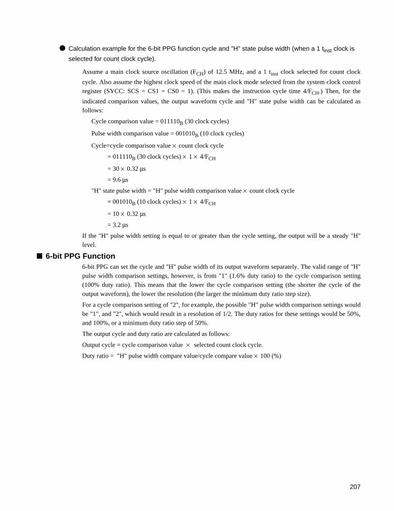
Calculation example for the 6-bit PPG function cycle and "H" state pulse width (when a 1 tinst clock is
selected for count clock cycle).
Assume a main clock source oscillation (FCH) of 12.5 MHz, and a 1 tinst clock selected for count clock
cycle. Also assume the highest clock speed of the main clock mode selected from the system clock control
register (SYCC: SCS = CS1 = CS0 = 1). (This makes the instruction cycle time 4/FCH.) Then, for the
indicated comparison values, the output waveform cycle and "H" state pulse width can be calculated as
follows:
Cycle comparison value = 011110B (30 clock cycles)
Pulse width comparison value = 001010B (10 clock cycles)
Cycle=cycle comparison value × count clock cycle
= 011110B (30 clock cycles) × 1 × 4/FCH
= 30 × 0.32 µs
= 9.6 µs
"H" state pulse width = "H" pulse width comparison value × count clock cycle
= 001010B (10 clock cycles) × 1 × 4/FCH
= 10 × 0.32 µs
= 3.2 µs
If the "H" pulse width setting is equal to or greater than the cycle setting, the output will be a steady "H"
level.
6-bit PPG Function6-bit PPG can set the cycle and "H" pulse width of its output waveform separately. The valid range of "H"
pulse width comparison settings, however, is from "1" (1.6% duty ratio) to the cycle comparison setting
(100% duty ratio). This means that the lower the cycle comparison setting (the shorter the cycle of the
output waveform), the lower the resolution (the larger the minimum duty ratio step size).
For a cycle comparison setting of "2", for example, the possible "H" pulse width comparison settings would
be "1", and "2", which would result in a resolution of 1/2. The duty ratios for these settings would be 50%,
and 100%, or a minimum duty ratio step of 50%.
The output cycle and duty ratio are calculated as follows:
Output cycle = cycle comparison value × selected count clock cycle.
Duty ratio = "H" pulse width compare value/cycle compare value × 100 (%)
207
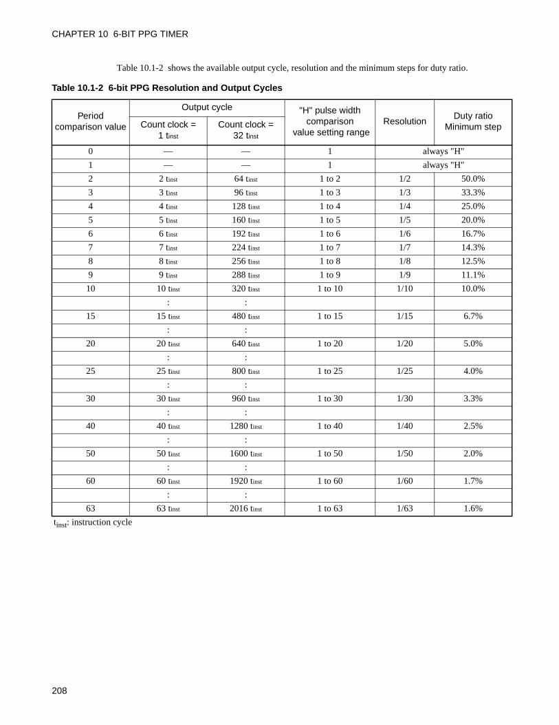
CHAPTER 10 6-BIT PPG TIMER
Table 10.1-2 shows the available output cycle, resolution and the minimum steps for duty ratio.
Table 10.1-2 6-bit PPG Resolution and Output Cycles
Period comparison value
Output cycle "H" pulse width comparison
value setting rangeResolution
Duty ratio Minimum stepCount clock =
1 tinst
Count clock =32 tinst
0 — — 1 always "H"
1 — — 1 always "H"
2 2 tinst 64 tinst 1 to 2 1/2 50.0%
3 3 tinst 96 tinst 1 to 3 1/3 33.3%
4 4 tinst 128 tinst 1 to 4 1/4 25.0%
5 5 tinst 160 tinst 1 to 5 1/5 20.0%
6 6 tinst 192 tinst 1 to 6 1/6 16.7%
7 7 tinst 224 tinst 1 to 7 1/7 14.3%
8 8 tinst 256 tinst 1 to 8 1/8 12.5%
9 9 tinst 288 tinst 1 to 9 1/9 11.1%
10 10 tinst 320 tinst 1 to 10 1/10 10.0%
: :
15 15 tinst 480 tinst 1 to 15 1/15 6.7%
: :
20 20 tinst 640 tinst 1 to 20 1/20 5.0%
: :
25 25 tinst 800 tinst 1 to 25 1/25 4.0%
: :
30 30 tinst 960 tinst 1 to 30 1/30 3.3%
: :
40 40 tinst 1280 tinst 1 to 40 1/40 2.5%
: :
50 50 tinst 1600 tinst 1 to 50 1/50 2.0%
: :
60 60 tinst 1920 tinst 1 to 60 1/60 1.7%
: :
63 63 tinst 2016 tinst 1 to 63 1/63 1.6%
tinst: instruction cycle
208

10.2 Block Diagram of 6-bit PPG Timer
The 6-bit PPG timer consists of the following five blocks:• Count clock selector• 6-bit counter• Comparator circuit• 6-bit PPG control register 1 (PPGC1)• 6-bit PPG control register 2 (PPGC2)
Block Diagram of 6-bit PPG timer
Figure 10.2-1 Block Diagram of 6-bit PPG timer
PPGC2 RCEN — SCL5 SCL4 SCL3 SCL2 SCL1 SCL0
Internal data bus
PPGC1 RCK1 RCK0 HSC5 HSC4 HSC3 HSC2 HSC1 HSC0
1 tinst
Count clock selector× 1/2× 1× 8× 32
6-bit counterCLK
CLEAR
Comparator circuit
6
6
Internal data bus
Period comparison value
6-bit PPG output enable signal
"H" pulse width comparison value
Pin
P06/INT26/PPG
6-bit PPGoutput
tinst: Instruction cycle
209
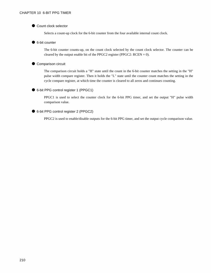
CHAPTER 10 6-BIT PPG TIMER
Count clock selector
Selects a count-up clock for the 6-bit counter from the four available internal count clock.
6-bit counter
The 6-bit counter counts-up, on the count clock selected by the count clock selector. The counter can be
cleared by the output enable bit of the PPGC2 register (PPGC2: RCEN = 0).
Comparison circuit
The comparison circuit holds a "H" state until the count in the 6-bit counter matches the setting in the "H"
pulse width compare register. Then it holds the "L" state until the counter count matches the setting in the
cycle compare register, at which time the counter is cleared to all zeros and continues counting.
6-bit PPG control register 1 (PPGC1)
PPGC1 is used to select the counter clock for the 6-bit PPG timer, and set the output "H" pulse width
comparison value.
6-bit PPG control register 2 (PPGC2)
PPGC2 is used to enable/disable outputs for the 6-bit PPG timer, and set the output cycle comparison value.
210

10.3 Pin of 6-bit PPG Timer
The section describes the pin, pin block diagram and register of the 6-bit PPG timer.
Pin of 6-bit PPG TimerThe 6-bit PPG uses the P06/INT26/PPG pin. The pin can function as general purpose I/O port (P06), as the
remote control output (PPG), or as a external interrupt input (INT26).
PPG:
When the output enable bit in the 6-bit PPG control register is set to "1" (PPGC2: RCEN = 1), this pin
functions as the 6-bit PPG timer pin, outputting a waveform having a "H" state pulse width and cycle as set.
Block Diagram of 6-bit PPG Timer Pin
Figure 10.3-1 Block Diagram of 6-bit PPG Timer Pin
Note:
When pull-up resistor is selected in pull-up register, the states of these pins in stop and watch mode(SPL=1) are in "H" level (pull-up state) rather than high impedance. However, during reset, pull-up isunavailable and will be in high impedance state.
DDR
Inte
rnal
dat
a bu
s
PDR read
PDR read (for bit manipulation instructions)
PDR write
DDR write (Port direction register)
Pull-up resistorApprox. 50 kΩ
Pin
SPL: Pin state specification bit in the standby control register (STBC)
N-ch
P-ch
P-ch
Stop, watch mode (SPL = 1)
Pull-up resistorcontrol register
Output latch
P06/INT26/PPG
From 6-Bit PPG output
From output control bitPPGC2: RCEN
Stop, watch mode
PDR (Port data register)
211
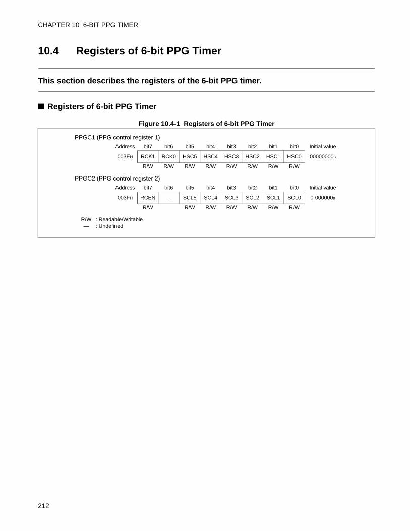
CHAPTER 10 6-BIT PPG TIMER
10.4 Registers of 6-bit PPG Timer
This section describes the registers of the 6-bit PPG timer.
Registers of 6-bit PPG Timer
Figure 10.4-1 Registers of 6-bit PPG Timer
PPGC1 (PPG control register 1)
PPGC2 (PPG control register 2)
Address bit7 bit6 bit5 bit4 bit3 bit2 bit1 bit0 Initial value
003EH RCK1 RCK0 HSC5 HSC4 HSC3 HSC2 HSC1 HSC0 00000000B
R/W R/W R/W R/W R/W R/W R/W R/W
Address bit7 bit6 bit5 bit4 bit3 bit2 bit1 bit0 Initial value
003FH RCEN — SCL5 SCL4 SCL3 SCL2 SCL1 SCL0 0-000000B
R/W R/W R/W R/W R/W R/W R/W
R/W : Readable/Writable— : Undefined
212
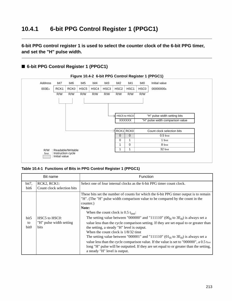
10.4.1 6-bit PPG Control Register 1 (PPGC1)
6-bit PPG control register 1 is used to select the counter clock of the 6-bit PPG timer, and set the "H" pulse width.
6-bit PPG Control Register 1 (PPGC1)
Figure 10.4-2 6-bit PPG Control Register 1 (PPGC1)
Table 10.4-1 Functions of Bits in PPG Control Register 1 (PPGC1)
Bit name Function
bit7,bit6
RCK2, RCK1:Count clock selection bits
Select one of four internal clocks as the 6-bit PPG timer count clock.
bit5to
bit0
HSC5 to HSC0:"H" pulse width setting bits
These bits set the number of counts for which the 6-bit PPG timer output is to remain "H". (The "H" pulse width comparison value to be compared by the count in the counter.)Note:
When the count clock is 0.5 tinst:The setting value between "000000" and "111110" (00H to 3EH) is always set a value less than the cycle comparison setting. If they are set equal to or greater than the setting, a steady "H" level is output.When the count clock is 1/8/32 tinstThe setting value between "000001" and "111110" (01H to 3EH) is always set a value less than the cycle comparison value. If the value is set to "000000", a 0.5 tinst long "H" pulse will be outputted. If they are set equal to or greater than the setting, a steady "H" level is output.
Address bit7 bit6 bit5 bit4 bit3 bit2 bit1 bit0 Initial value
003EH RCK1 RCK0 HSC5 HSC4 HSC3 HSC2 HSC1 HSC0 00000000B
R/W R/W R/W R/W R/W R/W R/W R/W
HSC5 to HSC0 "H" pulse width setting bits
XXXXXX "H" pulse width comparison value
RCK1 RCK0 Count clock selection bits
0 0 0.5 tinst
0 1 1 tinst
1 0 8 tinst
1 1 32 tinstR/W : Readable/Writabletinst : Instruction cycle
: Initial value
213
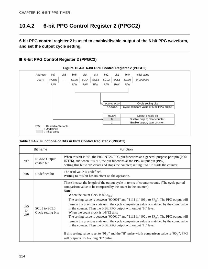
CHAPTER 10 6-BIT PPG TIMER
10.4.2 6-bit PPG Control Register 2 (PPGC2)
6-bit PPG control register 2 is used to enable/disable output of the 6-bit PPG waveform, and set the output cycle setting.
6-bit PPG Control Register 2 (PPGC2)
Figure 10.4-3 6-bit PPG Control Register 2 (PPGC2)
Table 10.4-2 Functions of Bits in PPG Control Register 2 (PPGC2)
Bit name Function
bit7RCEN: Output enable bit
When this bit is "0", the P06/INT26/PPG pin functions as a general-purpose port pin (P06/INT26), and when it is "1", the pin functions as the PPG output pin (PPG).Setting this bit to "0" clears and stops the counter; setting it to "1" starts the counter.
bit6 Undefined bitThe read value is undefined.Writing to this bit has no effect on the operation.
bit5to
bit0
SCL5 to SCL0: Cycle setting bits
These bits set the length of the output cycle in terms of counter counts. (The cycle period comparison value to be compared by the count in the counter.)Note:
When the count clock is 0.5 tinst
The setting value is between "000001" and "111111" (01H to 3FH). The PPG output will remain the previous state until the cycle comparison value is matched by the count value in the counter. Then the 6-Bit PPG output will output "H" level.When the count clock is 1/8/32 tinstThe setting value is between "000010" and "111111" (02H to 3FH). The PPG output will remain the previous state until the cycle comparison value is matched by the count value in the counter. Then the 6-Bit PPG output will output "H" level.
If this setting value is set to "01H" and the "H" pulse width comparison value is "00H", PPG will output a 0.5 tinst long "H" pulse.
Address bit7 bit6 bit5 bit4 bit3 bit2 bit1 bit0 Initial value
003FH RCEN — SCL5 SCL4 SCL3 SCL2 SCL1 SCL0 0-000000B
R/W R/W R/W R/W R/W R/W R/W
SCL5 to SCL0 Cycle setting bitsXXXXXX Cycle compare value of 6-bit PPG output
RCEN Output enable bit0 Disable output; clear counter.1 Enable output; start counter.
R/W : Readable/Writable— : Undefined
: Initial value
214

10.5 Operation of 6-bit PPG Timer
The 6-bit PPG timer generates a pulse in which the cycle and "H" state pulse width of the output can be set separately.
Operation of 6-bit PPG TimerFigure 10.5-1 shows the settings required to operate the 6-bit PPG timer.
Figure 10.5-1 6-bit PPG Timer Settings
Interval time
When the 6-bit PPG output is enabled, its 6-bit counter starts counting up from "0" in synchronization with
the selected count clock. During the first cycle, the PPG pin output will remain in "H" level until the count
in the counter matches the "H" state pulse width comparison value. When this happens, the PPG pin goes
"L" level and stays there until the count matches the cycle period comparison value, at which time the 6-bit
counter is cleared to "0" and continues to count. The fact that the pulse width and period can be set
separately enables the circuit to be used as a 6-bit PPG.
Figure 10.5-2 shows the operation of the 6-bit PPG timer.
bit7 bit6 bit5 bit4 bit3 bit2 bit1 bit0
PPGC1 RCK1 RCK0 HSC5 HSC4 HSC3 HSC2 HSCD1 HSC0
PPGC2 RCEN — SCL5 SCL4 SCL3 SCL2 SCL1 SCL0
1
: Used bit1: Set "1".0: Set "0".
215

CHAPTER 10 6-BIT PPG TIMER
Figure 10.5-2 Operation of 6-bit PPG Timer
00H
Counter value Cycle setting value (PPGC2: SCL0 to SCL5)
"H" pulse width setting value (PPGC1: HSC0 to HSC5)
Period*1
"H" Pulse Width*2
*1 : When count clock is 0.5 tinst
Period = 0.5 tinst x (Period comparison value + 1) When count clock is 1/8/32 tinst
Period = Count clock period x Period comparison value
*2: When count clock is 0.5 tinst
Pulse width = 0.5 tinst x ("H" pulse width comparison value + 1) When count clock is 1/8/32 tinst
Pulse width = Count clock period x "H" pulse width comparison value
PPG output waveform
216

10.6 Notes on Using 6-bit PPG Timer
This section lists points to note when using the 6-bit PPG timer.
Notes on Using 6-bit PPG Timer
"H" pulse width restrictions
Generally, the "H" pulse width setting bits of 6-bit PPG control register 1 (PPGC1: HSC5 to HSC0) must
always be set less than the cycle setting bits of PPG control register 2 (PPGC2: SCL5 to SCL0).
For any count clock, when SCL5 to SCL0 is "00H", HSC5 to HSC0 is equal to SCL5 to SCL0, or HSC5 to
HSC0 is larger than SCL5 to SCL0, the PPG pin will remain at steady "H" level.
For any count clock, when HSC5 to HSC0 is "00H" and SCL5 to SCL0 is not equal to "00H", the PPG pin
will start to output "L" level and then output a 0.5 tinst long "H" pulse after every cycle match is detected.
Resolution
When count clock is 0.5 tinst, the maximum "H" pulse width resolution is 1/64 of the cycle (the resolution
when the cycle setting is "111111" (3FH). Reducing the time of the cycle reduces the resolution, with the
minimum resolution of 1/2 occurring with a cycle setting of "000001" (01H).When count clock is 1/8/32
tinst, the maximum "H" pulse width resolution is 1/63 of the cycle (the resolution when the cycle setting is
"111111" (3FH). Reducing the time of the cycle reduces the resolution, with the minimum resolution of 1/2
occurring with a cycle setting of "000010" (02H).
Changing settings during operation
Direct comparisons are performed between the 6-bit counter of the 6-bit PPG waveform frequency and the
"H" pulse width setting bits (PPGC1: HSC5 to HSC0), and between the counter and the cycle setting bits
(PPGC2: SCL5 to SCL0). Therefore, if a setting is reduced in mid-count, the cycle time(t1) may be long
until the counter overflows in the worst case and takes effect in next cycle. Similarly, the "H" state pulse
width(t2) may be long in the worst case until the next end-of-cycle match is detected.
Figure 10.6-1 illustrates what happens when settings are changed during 6-bit PPG timer operation.
217
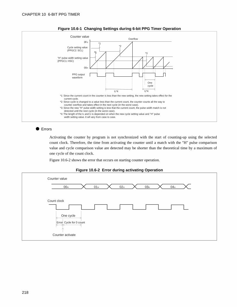
CHAPTER 10 6-BIT PPG TIMER
Figure 10.6-1 Changing Settings during 6-bit PPG Timer Operation
Errors
Activating the counter by program is not synchronized with the start of counting-up using the selected
count clock. Therefore, the time from activating the counter until a match with the "H" pulse comparison
value and cycle comparison value are detected may be shorter than the theoretical time by a maximum of
one cycle of the count clock.
Figure 10.6-2 shows the error that occurs on starting counter operation.
Figure 10.6-2 Error during activating Operation
*3*1
*1*2
00H
*1
3FH
Counter valueOverflow
Cycle setting value (PPGC2: SCL)
"H" pulse width setting value (PPGC1: HSC)
PPG output waveform
One cycle
*1: Since the current count in the counter is less than the new setting, the new setting takes effect for the current cycle.*2: Since cycle is changed to a value less than the current count, the counter counts all the way to counter overflow and takes effect in the next cycle (in the worst case).*3: Since the new "H" pulse width setting is less that the current count, the pulse width match is not detected until the next cycle (in the worst case).*4: The length of the t1 and t2 is depended on when the new cycle setting value and "H" pulse width setting value. It wll vary from case to case.
t1*4 t2*4
One cycle
Counter activate
Error
Counter value
Count clock
00H 01H 02H 03H 04H
Cycle for 0 count
218

10.7 Program Example for 6-bit PPG Timer
This section gives a program example for the 6-bit PPG timer.
Programming Example for 6-bit PPG Timer
Processing description
• Generate the 6-bit PPG at a cycle of approximately 12 µs and a 33% duty ratio.
• With a main clock source oscillation (FCH) of 12.5 MHz, the highest clock speed (speed shift function),
and the 1 tinst clock selected (1 instruction cycle time = 4/FCH), the comparison value for a cycle of
approximately 12 µs is as found as follows:
Cycle comparison value (PPGC2: SCL5 to SCL0) = 12 µs/(1 × 4/12.5 MHz) = 37.5
• The comparison value for a "H" state pulse width to provide a 33% duty ratio is found as follows:
"H" pulse width comparison value (PPGC1: HSC5 to HSC0) = 33/100 × cycle comparison value
= 0.33 × 37.5 = 12
Coding example
PPGC1 EQU 003EH ; PPG control register 1
PPGC2 EQU 003FH ; PPG control register 2
;----- Main program -------------------------------------------------------------------------------------------------------
CSEG ; [CODE SEGMENT]
:
MOV PPGC1,#01001100B; Select 1 tinst count clock, set "H" pulse width comparison
; value.
MOV PPGC2,#10100101B; Enable output and start counter, set cycle period,
; comparison value.
:
ENDS
;--------------------------------------------------------------------------------------------------------------------------------
END
219

CHAPTER 10 6-BIT PPG TIMER
220

CHAPTER 118/16-BIT TIMER/COUNTER
This chapter describes the functions and operation of the 8/16-bit timer/counter.
11.1 Overview of 8/16-bit Timer/Counter
11.2 Block Diagram of 8/16-bit Timer/Counter
11.3 Pins of 8/16-bit Timer/Counter
11.4 Registers of 8/16-bit Timer/Counter
11.5 8/16-bit Timer/Counter Interrupt
11.6 Operation of Interval Timer Function
11.7 Operation of Counter Function
11.8 Operation of the Square Wave Output Initial Setting Function
11.9 Operation of 8/16-bit Timer/Counter Stop and Restart
11.10 States in Each Mode during 8/16-bit Timer/Counter Operation
11.11 Notes on Using 8/16-bit Timer/Counter
11.12 Program Examples for 8/16-bit Timer/Counter
221
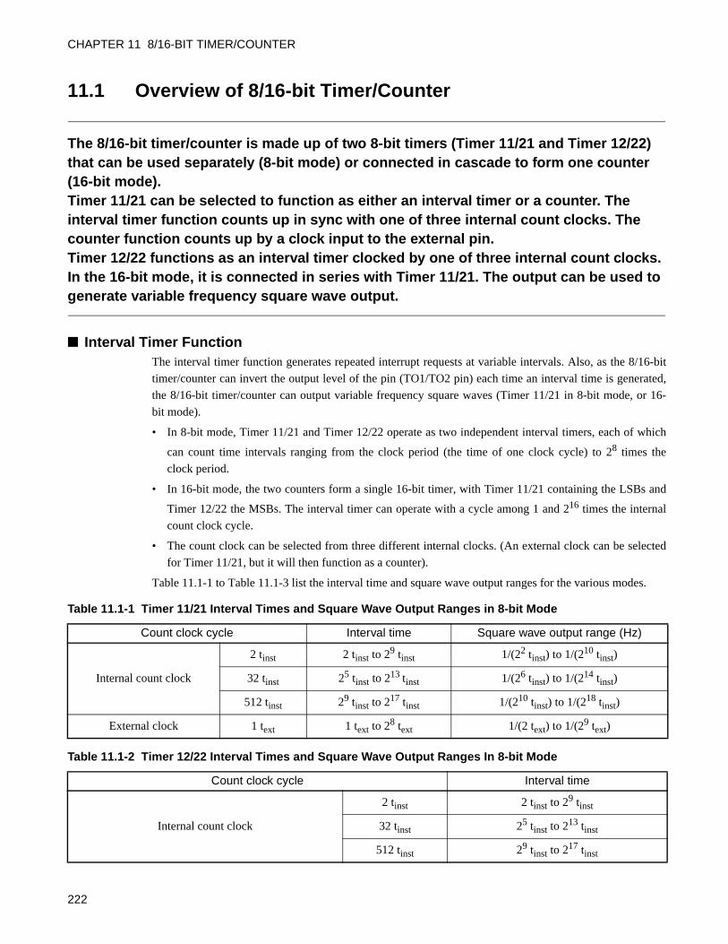
CHAPTER 11 8/16-BIT TIMER/COUNTER
11.1 Overview of 8/16-bit Timer/Counter
The 8/16-bit timer/counter is made up of two 8-bit timers (Timer 11/21 and Timer 12/22) that can be used separately (8-bit mode) or connected in cascade to form one counter (16-bit mode).Timer 11/21 can be selected to function as either an interval timer or a counter. The interval timer function counts up in sync with one of three internal count clocks. The counter function counts up by a clock input to the external pin. Timer 12/22 functions as an interval timer clocked by one of three internal count clocks. In the 16-bit mode, it is connected in series with Timer 11/21. The output can be used to generate variable frequency square wave output.
Interval Timer FunctionThe interval timer function generates repeated interrupt requests at variable intervals. Also, as the 8/16-bit
timer/counter can invert the output level of the pin (TO1/TO2 pin) each time an interval time is generated,
the 8/16-bit timer/counter can output variable frequency square waves (Timer 11/21 in 8-bit mode, or 16-
bit mode).
• In 8-bit mode, Timer 11/21 and Timer 12/22 operate as two independent interval timers, each of which
can count time intervals ranging from the clock period (the time of one clock cycle) to 28 times the
clock period.
• In 16-bit mode, the two counters form a single 16-bit timer, with Timer 11/21 containing the LSBs and
Timer 12/22 the MSBs. The interval timer can operate with a cycle among 1 and 216 times the internal
count clock cycle.
• The count clock can be selected from three different internal clocks. (An external clock can be selected
for Timer 11/21, but it will then function as a counter).
Table 11.1-1 to Table 11.1-3 list the interval time and square wave output ranges for the various modes.
Table 11.1-1 Timer 11/21 Interval Times and Square Wave Output Ranges in 8-bit Mode
Count clock cycle Interval time Square wave output range (Hz)
Internal count clock
2 tinst 2 tinst to 29 tinst 1/(22 tinst) to 1/(210 tinst)
32 tinst 25 tinst to 213 tinst 1/(26 tinst) to 1/(214 tinst)
512 tinst 29 tinst to 217 tinst 1/(210 tinst) to 1/(218 tinst)
External clock 1 text 1 text to 28 text 1/(2 text) to 1/(29 text)
Table 11.1-2 Timer 12/22 Interval Times and Square Wave Output Ranges In 8-bit Mode
Count clock cycle Interval time
Internal count clock
2 tinst 2 tinst to 29 tinst
32 tinst 25 tinst to 213 tinst
512 tinst 29 tinst to 217 tinst
222

Calculation example for the interval time and square wave frequency
In this example, the main clock source oscillation (FCH) is 12.5 MHz, the Timer 11/21 data register
(T11DR/T21DR) value is set to "DDH (221)", and the count clock cycle is set to the 8-bit mode
operation at 2 tinst. In this case, the Timer 11/21 interval time and frequency of square wave output from
the TO1/TO2 pin are calculated as follows.
Assume that the highest clock speed has been selected via the system clock control register (SYCC:
CS1 = 1, CS0 = 1) (1 instruction cycle = 4/FCH).
Interval time = (2 × 4/FCH) × (T11DR/T21DR register value + 1)
= (8/12.5 MHz) × (221 + 1)
= approx. 142.08µs
Output frequency = FCH/(2 × 8 × (T11DR/T21DR register value + 1))
= 12.5 MHz/ (16 × (221 + 1))
= approx. 3.52 kHz
Counter FunctionThe counter function counts falling edges of an external count clock applied to the external pin (EC1, EC2
pin). Since the external clock can be selected only for Timer 11/21, the counter function operates in either
timer 11/21 in the 8-bit mode or 16-bit mode.
• The counter counts up, clocked by external clocks. When the count equals the set value, it generates an
interrupt request in both 8-bit and 16-bit mode and inverts the level being output at the TO1/TO2 pin.
• In the 8-bit mode, Timer 11/21 can count as high as 28.
• In the 16-bit mode, the function counts as high as 216.
• By injecting an external clock having a set period, the counter function can be used the same way as the
interval timer function.
Table 11.1-3 Interval Times and Square Wave Output Ranges in 16-bit mode
Count clock cycle Interval Time Square wave output range (Hz)
Internal count clock 2 tinst 2 tinst to 217 tinst 1/(22 tinst) to 1/(218 tinst)
32 tinst 25 tinst to 221 tinst 1/(26 tinst) to 1/(222 tinst)
512 tinst 29 tinst to 225 tinst 1/(210 tinst) to 1/(226 tinst)
External clock 1 text 1 text to 216 text 1/(2 text) to 1/(217 text)
tinst: Instruction cycle (affected by clock mode, etc.)text: External clock period
223

CHAPTER 11 8/16-BIT TIMER/COUNTER
11.2 Block Diagram of 8/16-bit Timer/Counter
The 8/16-bit timer/counter consists of the following five blocks:• Count clock selectors 1 and 2• Counter circuits 1 and 2• Square wave output controller• Timer data registers (T11DR, T12DR, T21DR, T22DR)• Timer control registers (T11CR, T12CR, T21CR, T22CR)
Block Diagram of 8/16-bit Timer/Counter
Figure 11.2-1 Block Diagram 8/16-bit Timer/Counter
T1STR T1STP T1CS0 T1CS1 T1OS0 T1OS1 T1IE T1IFT11CR
T2STR T2STP T2CS0 T2CS1 T2OS0 T2OS1 T2IE T2IFT12CR
T.FF
/2 R,S
CKQ
2/
1tinst× 2× 32× 512
1tinst× 2× 32× 512
P27/V2/EC1
/2
CKCLR
CO
EQ
LOAD
LOAD
EQ
CKCLR
Square wave output controller
Initialize pin control/output
Interrupt requestIRQ6IRQ7
Count clock selector 1
Count clock selector 2
Counter circuit 1
Counter circuit 2
8-bit counter
T11DR/T21DR read
Inte
rnal
dat
a bu
s
Comparator
Comparison data latch
Data register
Data register
Comparison data latchComparator
8-bit counter
Pin
T12DR/T22DR read
Pin
P26/V1/TO1P24/C1/TO2*
tinst : Instructin cycle* : If booster is selected, EC2 and TO2 will be redireted to P03/INT23 and P04/INT24 respectively.
T21CR
P25/C0/EC2*
T22CR
Outputenablesignal
T11DR/T21DR and T12DR/T22DR Write
224

Count clock selectors 1, 2
This circuit selects an input clock. In timer 11/21 in the 8-bit and 16 bit modes, count clock selector 1
selects one of four clocks: three internal clocks, and an external clock. In the 8-bit mode, count Clock
Selector 2 selects one of three internal clocks only.
Counter circuits 1, 2
• Counter circuit 1 and counter circuit 2 are each made up of an 8-bit counter, a comparator, a comparisondata latch, and a data register (T11DR/T21DR or T12DR/T22DR).
• In each counter circuit, the 8-bit counter counts up clocked by the selected count clock. The comparatorcompares the count in the counter with the value in the comparison data latch. When it detects a match,it clears the counter, and loads the contents of the data register into the comparison data latch.
• In the 8 bit-mode, the two counter circuits operate independently as Timer 11/21 and timer 12/22. In the16-bit mode, the two circuits are connected in series to form a single 16-bit counter with counter circuit1 forming the lower (8 LSBs) end of the counter, and counter circuit 2 at the upper (8 MSBs) end.
Square wave output control circuit
• An interrupt request is generated when the comparator detects a match in the 8-bit mode or the 16-bitmode. At this time, if the square wave output is enabled, the output control circuit inverts the leveloutput at the TO1/TO2 pin. (only for 8-bit timer 11/21 in 8-bit mode or 16-bit mode)
• The circuit can also initialize the output level to have the output square wave start out in a specific state("H" or "L") (only for 8-bit timer 11/21 in 8-bit mode or 16-bit mode).
Timer data registers (T11DR/T21DR and T12DR/T22DR)
The value to be compared with the count in the 8-bit counter is set by writing the desired value into these
registers. They can be read to determine the current counter values.
Timer control registers(T11CR/T21CR and T12CR/T22CR)
These registers are used to select the function, to enable or disable operation, control interrupts, and check
the timer/counter status.
225
CHAPTER 11 8/16-BIT TIMER/COUNTER
11.3 Pins of 8/16-bit Timer/Counter
This section describes the pins, pin block diagram, registers, and interrupt source of the 8/16-bit timer/counter.
Pins of 8/16-bit Timer/CounterThe 8/16-bit timer/counter 11,12 uses the P27/V2/EC1 pin and P26/V1/TO1 pin. The 8/16-bit timer/counter
21,22 uses the P25/C0/EC2 and P24/C1/TO2 pins. The P27/V2/EC1, P25/C0/EC2 pins can function as a
general-purpose I/O port (P25, P27) or external clock input pin of timer(EC1, EC2). The P26/V1/TO1, P24/
C1/TO2 pins can function as a general-purpose I/O port (P24, P26) or the square wave output pin of timer
(TO1, TO2).
EC1 and EC2:
In timer 11/21 in the 8-bit mode or 16-bit mode, if external clock input (counter function) is selected
(T11CR/T21CR: T1CS1 = 1, T1CS0 = 1), the counter counts the external clocks applied to this pin. The
P27/V2/EC1, P25/C0/EC2 pins set the pin as an input port in the port direction register (DDR2: bit5, bit7 =
0) when using as the EC1 and EC2 pins.
TO1 and TO2:
In timer 11/21 in the 8-bit mode or 16-bit mode, a square wave is output at this pin. Enabling square wave
output (T11CR/T21CR: T1OS1, T1OS0 = 11B) automatically sets the P26/V1/TO1, P24/C1/TO2 pins as an
output pin, regardless of the port direction register (DDR2: bit5, bit7) value, and sets the pin to function as
the TO1, TO2 pins.
226

Block Diagram of 8/16-bit Timer Counter Pins
Figure 11.3-1 Block Diagram of 8/16-bit Timer Counter Pins (P24, P25)
Figure 11.3-2 Block Diagram of 8/16-bit Timer/Counter Pins (P26, P27)
PDR (Port data register)
DDR
Inte
rnal
dat
a bu
s
PDR read
PDR read (for bit manipulation instructions)
Output latch
PDR write
DDR write
Pin
* : If booster is selected by mask option, EC2 and TO2 will be redirected to P03 and P04 respectively.SPL: Pin state specification bit in the standby control register (STBC)
N-ch
Stop, watch mode
External clock input (EC2)
(Port direction register)
DDR read
Stop, watch mode
Maskoption *
(SPL = 1)
Timer output (TO2)
Timer output enable
Booster
Maskoption *
P24/C1/TO2*P25/C0/EC2*
PDR (Port data register)
DDR
Inte
rnal
dat
a bu
s
PDR read
PDR read (for bit manipulation instructions)
Output latch
PDR write
DDR write
Pin
SPL: Pin state specification bit in the standby control register (STBC)
N-ch
Stop, watch mode
External clock input (EC1)
(Port direction register)
DDR read
Stop, watch mode
(SPL = 1)
Timer output (TO1)
Timer output enable
LCD driver/booster
LCD pin select
P26/V1/TO1P27/V2/EC1
N-ch
227
CHAPTER 11 8/16-BIT TIMER/COUNTER
11.4 Registers of 8/16-bit Timer/Counter
This section describes the registers of the 8/16-bit timer/counter.
Registers of 8/16-bit Timer/Counter
Figure 11.4-1 Registers of 8/16-bit Timer/Counter
Interrupt Source of 8/16-bit Timer/CounterIRQ6:
In the interval timer and counter functions for timer 11 in 8-bit mode or 16-bit mode, timer 12 in 8-bit
mode, if the interrupt request output is enabled, an IRQ6 interrupt request will be generated when the count
in the counter equals the value set in the data register. Interrupt request outputs are enabled by setting the
proper timer control register bit (T11CR: T1IE = 1 in Timer 11 in 8-bit mode or 16-bit mode, T12CR:
T2IE = 1 in Timer 12 in 8-bit mode).
IRQ7:
In the interval timer and counter functions for timer 21 in 8-bit mode or 16-bit mode, timer 22 in 16-bit
modes, if the interrupt request output is enabled, an IRQ7 interrupt request will be generated when the
count in the counter equals the value set in the data register. Interrupt request outputs are enabled by setting
the proper timer control register bit (T21CR: T1IE = 1 in Timer 21 in 8-bit mode or 16-bit mode, T22CR:
T2IE = 1 in Timer 22 in 8-bit mode).
T11CR/T21CR (Timer 11/21 control register)
T12CR/T22CR (Timer 12/22 control register)
T11DR/T21DR (Timer 11/21 data register)
T12DR/T22DR (Timer 12/22 data register)
Address bit7 bit6 bit5 bit4 bit3 bit2 bit1 bit0 Initial value003BH
0037H T1IF T1IE T1OS1 T1OS0 T1CS1 TS1CS0 T1STP T1STR 000000X0B
R/W R/W R/W R/W R/W R/W R/W R/W
Address bit7 bit6 bit5 bit4 bit3 bit2 bit1 bit0 Initial value003AH
0036H T2IF T2IE T2OS1 T2OS0 T2CS1 T2CS0 T2STP T2STR 000000X0B
R/W R/W R/W R/W R/W R/W R/W R/W
Address bit7 bit6 bit5 bit4 bit3 bit2 bit1 bit0 Initial value003DH
0039HXXXXXXXXB
R/W R/W R/W R/W R/W R/W R/W R/W
Address bit7 bit6 bit5 bit4 bit3 bit2 bit1 bit0 Initial value003CH
0038HXXXXXXXXB
R/W R/W R/W R/W R/W R/W R/W R/W
R/W : Readable/WritableX : Undefined value
228
11.4.1 Timer 11/21 Control Register (T11CR/T21CR)
In Timer 11/21 in the 8-bit mode and in the 16-bit mode, the timer 11/21 control register (T11CR/T21CR) is used to select functions, to enable/disable operation, to control interrupts, and to check status. In the 8-bit mode, the timer 12/22 control register (T12CR/T22CR) must still be initialized, even only Timer 11/21 is used.
Timer 11/21 Control Register (T11CR/T21CR)
Figure 11.4-2 Timer 11/21 Control Register (T11CR/T21CR)
Address bit7 bit6 bit5 bit4 bit3 bit2 bit1 bit0 Initial value
003BH
0037HT1IF T1IE T1OS1 T1OS0 T1CS1 T1CS0 T1STP T1STR 000000X0B
R/W R/W R/W R/W R/W R/W R/W R/W
T1STR Timer activation bit
0 Stops counter
1 Clears counter, then starts it
T1STP Timer stop bit
0 Causes counter to resume counting without clearing
1 Temporarily stops counter
T1CS1 T1CS0Count clock selection bits
(tinst: instruction cycle)
0 0 2 tinst
0 1 32 tinst
1 0 512 tinst
1 1 External clock
T1OS1 T1OS0 Square wave output control bits
0 0 Use pin for general-purpose port
0 1 Set data to output square wave "L" state
1 0 Set data to output square wave "H" state
1 1Output set level at square wave output pin (TO1/TO2)
T1IE Interrupt request enable bit
0 Disable interrupt request output
1 Enable interrupt request output
T1IFInterrupt request Flag Bit
Read Write
0 No counter match Clears this bit
1 Have counter match No effect: The bit does not change.
*: The square wave output pin will go to the level corresponding to data set when T1STR is "0".
R/W : Readable/WritableX : Undefined value
: Initial value
229

CHAPTER 11 8/16-BIT TIMER/COUNTER
Note:
Before using 8/16-bit timer/counter Timer 11/21 only in 8-bit mode, first set the timer count clockselection bits of the Timer 12/22 control register (T12CR/T22CR: T2CS1, T2CS0) to some stateother than "11B". Operating in this mode without making this register setting could result in faultyoperation.
Table 11.4-1 Timer 11/21 Control Register (T11CR/T21CR) Bits
Bit name Function
bit7T1IF: Interrupt request flag bit
• 8 bit-mode:Set to "1" when the count in the timer 11/21 counter matches the value set in the T11DR/T21DR, the timer 11/21 data register (comparison data latch).
• 16-bit mode:Set to "1" when the counts in the timer 11/21 and timer 12/22 counters match the values set in the T11DR/T21DR and T12DR/T22DR registers, respectively.
• An interrupt request is output when both this bit and the interrupt request enable bit (T1IE) are "1".
• Writing "0" clears this bit. writing "1" has no effect and does not change the bit value.
bit6T1IE: Interrupt request enable bit
• This bit enables or disables an interrupt request output to the CPU.• An interrupt request is output when both this bit and the interrupt request flag bit
(T1IF) are "1".
bit5,bit4
T1OS1 and T1OS0:square wave output control bits
• P26/V1/TO1 or P24/C1/TO2 is a general-purpose I/O port pin (P24, P26) if both of these bits are "00B". If the bits are not "00B", it is the square wave output pin (TO1 or TO2).
• If written to "01B", or "10B", the initialize data will be set in the square wave output controller, but the corresponding level will not be output to the TO1 or TO2 pin.
• If both bits are "11B", and the function is in the stop timer state (T2STR= 0), the TO1 or TO2 pin is set to a level corresponding to the initialize data.
bit3,bit2
T1CS1 and T1CS0:Clock source selection bits
• Selects the count clock to be supplied to the counter.• Selects one of three internal clocks, or an external clock.• When both bits are "11B", Timer 11/21 operates as a counter with the external
clock is selected as the count clock.Note:
If external clock input is selected (T1CS1, T1CS0 = 11B), set the P27/V2/EC1, P25/C0/EC2 pin as an input port pin.
bit1T1STP: Timer stop bit
• This bit is used to temporarily stop the counter.• Writing this bit to "1" temporarily stops the counter. Writing it to "0" when the
timer in startup state (T1STR = 1), restarts the counter where it left off.
bit0T1STR:Timer activation bit
• Starts and stops timer.• Changing this bit from "0" to "1" clears the counter. At this time, if the timer is in
the continuous operation mode (T1STP = 0), the counter starts (counts up, clocked by the selected count clock). Writing this bit to "0" stops the counter.
• In the 16-bit mode, both Timer 11/21 and Timer 12/22 are cleared at timer start (T1STP = 0 -> 1).
230

11.4.2 Timer 12/22 Control Register (T12CR/T22CR)
In timer 12/22 in the 8-bit mode, the timer 12/22 control register (T12CR/T22CR) is used to select functions, to enable/disable operation, to control interrupts, and to check states. In the 16-bit mode, although the function is controlled by the timer 11/21 control register (T11CR/T21CR), the timer 12/22 control register (T12CR/T22CR) must still be set.
Timer 12/22 Control Register (T12CR/T22CR)
Figure 11.4-3 Timer 12/22 Control Register (T12CR/T22CR)
Address bit7 bit6 bit5 bit4 bit3 bit2 bit1 bit0 Initial value
003AH
0036HT2IF T2IE T2OS1 T2OS0 T2CS1 T2CS0 T2STP T2STR 000000X0B
R/W R/W R/W R/W R/W R/W R/W R/W
T2STR Timer activation bit
0 Stops counter
1 Clears counter, then starts it
T2STP Timer stop bit
0 Causes counter to resume counting without clearing
1 Temporarily stops counter
T2CS1 T2CS0 Count clock selection bits
0 0 2 tinst
0 1 32 tinst
1 0 512 tinst
1 1 16-bit mode
T2OS1 T2OS0 Unused bits
0 0
These two bits must set to "00B".Do not set to other value.
0 1
1 0
1 1
T2IE interrupt request enable bit
0 Disables interrupt request output
1 Enables interrupt request output
T2IFinterrupt request flag bit
Read Write
0 No counter match Clears this bit
1 Have counter match No effect: The bit does not change.
R/W : Readable/Writable
X : Undefined value
: Initial value
231
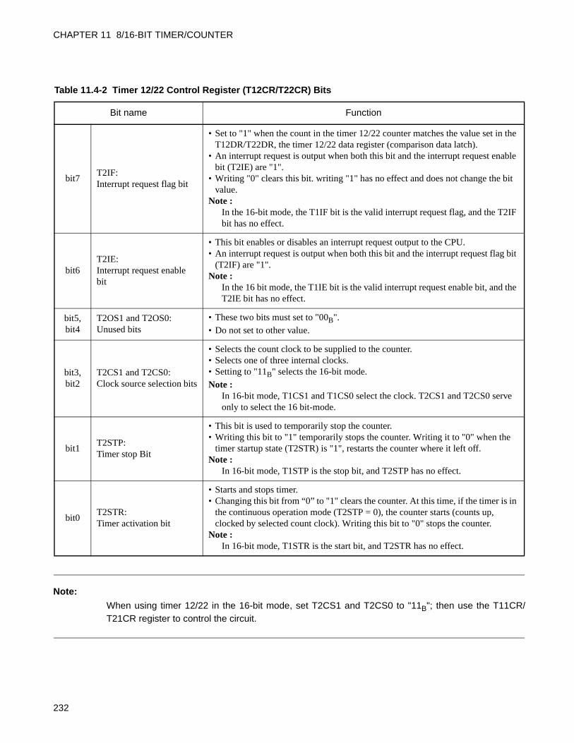
CHAPTER 11 8/16-BIT TIMER/COUNTER
Note:
When using timer 12/22 in the 16-bit mode, set T2CS1 and T2CS0 to "11B"; then use the T11CR/T21CR register to control the circuit.
Table 11.4-2 Timer 12/22 Control Register (T12CR/T22CR) Bits
Bit name Function
bit7T2IF:Interrupt request flag bit
• Set to "1" when the count in the timer 12/22 counter matches the value set in the T12DR/T22DR, the timer 12/22 data register (comparison data latch).
• An interrupt request is output when both this bit and the interrupt request enable bit (T2IE) are "1".
• Writing "0" clears this bit. writing "1" has no effect and does not change the bit value.
Note : In the 16-bit mode, the T1IF bit is the valid interrupt request flag, and the T2IF bit has no effect.
bit6T2IE:Interrupt request enable bit
• This bit enables or disables an interrupt request output to the CPU.• An interrupt request is output when both this bit and the interrupt request flag bit
(T2IF) are "1".Note :
In the 16 bit mode, the T1IE bit is the valid interrupt request enable bit, and the T2IE bit has no effect.
bit5,bit4
T2OS1 and T2OS0: Unused bits
• These two bits must set to "00B". • Do not set to other value.
bit3,bit2
T2CS1 and T2CS0:Clock source selection bits
• Selects the count clock to be supplied to the counter.• Selects one of three internal clocks.• Setting to "11B" selects the 16-bit mode.Note :
In 16-bit mode, T1CS1 and T1CS0 select the clock. T2CS1 and T2CS0 serve only to select the 16 bit-mode.
bit1T2STP: Timer stop Bit
• This bit is used to temporarily stop the counter.• Writing this bit to "1" temporarily stops the counter. Writing it to "0" when the
timer startup state (T2STR) is "1", restarts the counter where it left off.Note :
In 16-bit mode, T1STP is the stop bit, and T2STP has no effect.
bit0T2STR: Timer activation bit
• Starts and stops timer.• Changing this bit from “0” to "1" clears the counter. At this time, if the timer is in
the continuous operation mode (T2STP = 0), the counter starts (counts up, clocked by selected count clock). Writing this bit to "0" stops the counter.
Note : In 16-bit mode, T1STR is the start bit, and T2STR has no effect.
232
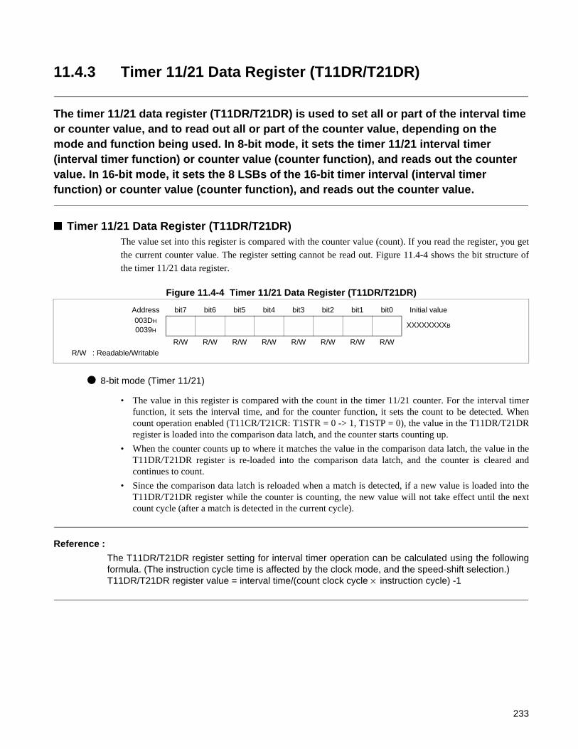
11.4.3 Timer 11/21 Data Register (T11DR/T21DR)
The timer 11/21 data register (T11DR/T21DR) is used to set all or part of the interval time or counter value, and to read out all or part of the counter value, depending on the mode and function being used. In 8-bit mode, it sets the timer 11/21 interval timer (interval timer function) or counter value (counter function), and reads out the counter value. In 16-bit mode, it sets the 8 LSBs of the 16-bit timer interval (interval timer function) or counter value (counter function), and reads out the counter value.
Timer 11/21 Data Register (T11DR/T21DR)The value set into this register is compared with the counter value (count). If you read the register, you get
the current counter value. The register setting cannot be read out. Figure 11.4-4 shows the bit structure of
the timer 11/21 data register.
Figure 11.4-4 Timer 11/21 Data Register (T11DR/T21DR)
8-bit mode (Timer 11/21)
• The value in this register is compared with the count in the timer 11/21 counter. For the interval timerfunction, it sets the interval time, and for the counter function, it sets the count to be detected. Whencount operation enabled (T11CR/T21CR: T1STR = 0 -> 1, T1STP = 0), the value in the T11DR/T21DRregister is loaded into the comparison data latch, and the counter starts counting up.
• When the counter counts up to where it matches the value in the comparison data latch, the value in theT11DR/T21DR register is re-loaded into the comparison data latch, and the counter is cleared andcontinues to count.
• Since the comparison data latch is reloaded when a match is detected, if a new value is loaded into theT11DR/T21DR register while the counter is counting, the new value will not take effect until the nextcount cycle (after a match is detected in the current cycle).
Reference :
The T11DR/T21DR register setting for interval timer operation can be calculated using the followingformula. (The instruction cycle time is affected by the clock mode, and the speed-shift selection.)T11DR/T21DR register value = interval time/(count clock cycle × instruction cycle) -1
Address bit7 bit6 bit5 bit4 bit3 bit2 bit1 bit0 Initial value003DH
0039HXXXXXXXXB
R/W R/W R/W R/W R/W R/W R/W R/WR/W : Readable/Writable
233

CHAPTER 11 8/16-BIT TIMER/COUNTER
16-bit mode
The value in this register is compared with the counter value for the lower 8 bits (LSBs) of the 16-bit timer.
In the interval timer function, this sets the lower 8 bits of the interval time setting, and in the counter
function, the lower 8 bits of the count to be detected. The contents of the T11DR/T21DR register are
loaded into the lower 8 bits of the comparison data latch when the counter first starts operating and when a
match is detected in the 16-bit count. Therefore, if a new value is loaded into the T11DR/T21DR register
while the 16-bit counter is counting, the new value will not take effect until after the next match is detected.
For information on T11DR/T21DR register settings in the interval timer mode, refer to "11.4.4 Timer 12/
22 Data Register (T12DR/T22DR)".
234

11.4.4 Timer 12/22 Data Register (T12DR/T22DR)
The timer 12/22 data register (T12DR/T22DR) is used to set all or part of the interval time or counter value, and to read out all or part of the counter value, depending on the mode and function being used. In 8-bit mode, it sets the Timer 12/22 interval timer (interval timer function) or counter value (counter function), and reads out the counter value. In 16-bit mode, it sets the 8 LSBs of the 16-bit timer interval (interval timer function) or counter value (counter function), and reads out the counter value.
Timer 12/22 Data Register (T12DR/T22DR)The value set into this register is compared with the counter value (count). If you read the register, you get
the current counter value. The register setting cannot be read out. Figure 11.4-5 shows the bit structure of
the timer 12/22 data register.
Figure 11.4-5 Timer 12/22 Data Register (T12DR/T22DR)
8-bit mode (Timer 12/22)
The value in this register is compared with the count in the timer 12/22 counter. For the interval timer
function, it sets the interval time, and for the counter function, it sets the count to be detected. The value in
the T12DR/T22DR register is reloaded into the comparison data latch when counter operation starts, and
when a match is detected.
If a new value is loaded into the T12DR/T22DR register while the counter is counting, the new value will
not take effect until the next count cycle (after a match is detected in the current cycle).
Reference :
The T12DR/T22DR register setting for interval timer operation can be calculated using the followingformula. (The instruction cycle time is affected by the clock mode, and speed-shift selection.)T12DR/T22DR register value = interval time/(count clock cycle × instruction cycle time) -1
Address bit7 bit6 bit5 bit4 bit3 bit2 bit1 bit0 Initial value003CH
0038HXXXXXXXXB
R/W R/W R/W R/W R/W R/W R/W R/W
R/W : Readable/Writable
235
CHAPTER 11 8/16-BIT TIMER/COUNTER
16-bit mode
The value in this register is compared with the counter value for the upper 8 bits (MSBs) of the 16-bit
timer. In the interval timer function, this sets the upper 8 bits of the interval time setting, and in the counter
function, the upper 8 bits of the count to be detected. The contents of the T12DR/T22DR register are
loaded into the upper 8 bits of the comparison data latch when the counter first starts operating and when a
match is detected in the 16-bit count. Therefore, if a new value is loaded into the T12DR/T22DR register
while the 16-bit counter is counting, the new value will not take effect until after the next match is detected.
In the 16-bit mode, the operation of the counter is controlled by the Timer 11/21 control register (T11CR/
T21CR).
Reference :
In the interval timer function, the T11DR/T21DR and T12DR/T22DR register settings can becalculated from the following formula. (The instruction cycle time is affected by the clock mode, andthe speed-shift selection.)16-bit data value = interval time/(count clock cycle × instruction cycle) -1The 8 MSBs of the 16-bit data value are the T12DR/T22DR register setting, and the 8 LSBs are theT11DR/T21DR register setting.
236

11.5 8/16-bit Timer/Counter Interrupt
In the 8/16-bit timer/counter, interrupt conditions are satisfied (if interrupts are enabled) when the counter matches the data register. This is true for both the interval timer and counter functions.
8/16-bit Timer/Counter InterruptTable 11.5-1 lists the interrupt request flag bit, interrupt request output enable bit, andinterrupt source of the 8/16-bit timer/counter.
In 8-bit mode, 8/16-bit timer/counter interrupt requests are generated independently for Timer 11/21 and
Timer 12/22. In 16-bit mode, the interrupt request is generated only for Timer 11/21, but basic operation is
the same. Interrupt operation will therefore be described only for Timer 11/21 in 8-bit mode.
8-bit Mode Timer 11/21 Interrupt OperationThe counter counts up from "00H", clocked by the selected count clock. When the count in the counter
matches the value in the comparison data latch (corresponding to the value in timer data register T11DR/
T21DR), the interrupt request flag bit is set to "1" (T11CR/T21CR: T1IF).
At this time, an interrupt request (IRQ6, IRQ7) to the CPU is generated if the interrupt request enable bit is
enabled (T11CR/T21CR: T1IE=1). Write "0" to the T1IF bit in the interrupt processing routine to clear the
interrupt request.
The T1IF bit is set to "1" when the counter value matches the set value, regardless of the value of the T1IE
bit.
Notes :
• The T1IF bit is not set if the counter is stopped (T11CR/T21CR: T1STR = 0) at the same time asthe counter value matches the T11DR/T21DR1 register.
• An interrupt request is generated immediately if the T1IF bit is "1" when the T1IE bit is changedfrom disabled to enabled ("0" -> "1").
Table 11.5-1 8/16-bit Timer/Counter Interrupt Control Bits and Interrupts
8-bit mode 16-bit mode
Timer 11/21 and Timer 12/22 Timer 11/21 Timer 12/22 Timer 11/12 + Timer 12/22
Interrupt request flag bit T11CR/T21CR:T1IF T12CR/T22CR:T2IF T11CR/T21CR:T1IF
interrupt request enable bit T11CR/T21CR:T1IE T12CR/T22CR:T2IE T11CR/T21CR:T1IE
Interrupt source8-bit counter matches
T11DR/T21DR8-bit counter matches
T12DR/T22DR
16-bit counter matches T11DR/T21DR
and T12DR/T22DR
237

CHAPTER 11 8/16-BIT TIMER/COUNTER
Registers and Vector Table for 8/16-bit Timer/Counter (11, 12, 21, 22) Interrupt
See "3.4.2 Interrupt Processing" for details on the interrupt operation.
Table 11.5-2 Registers and Vector Table for 8/16-bit Timer/Counter Interrupt
InterruptInterrupt level settings register Vector table address
Register Setting bits Upper Lower
IRQ6 (Timer ch.1) ILR2 (007CH) L61 (bit5) L60 (bit4) FFEEH FFEFH
IRQ7 (Timer ch.2) ILR2 (007CH) L71 (bit7) L70 (bit6) FFECH FFEDH
238
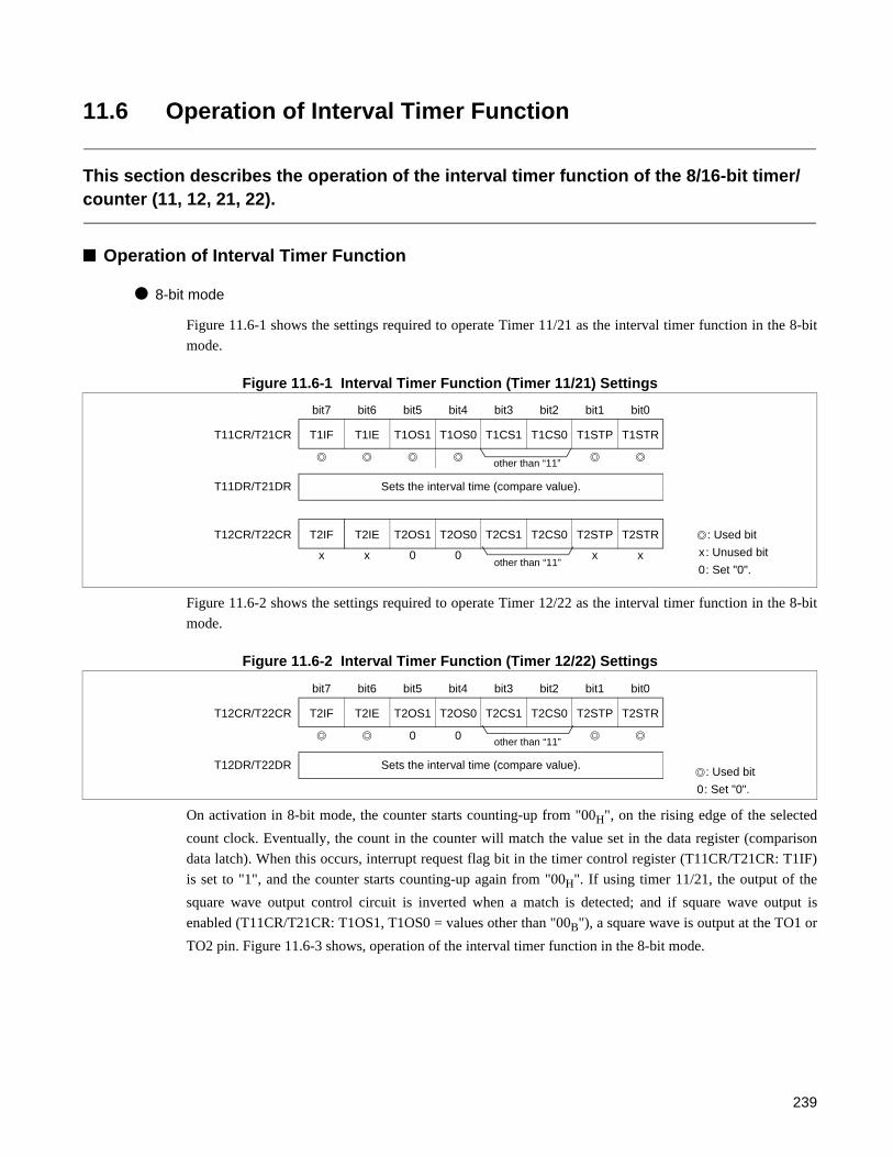
11.6 Operation of Interval Timer Function
This section describes the operation of the interval timer function of the 8/16-bit timer/counter (11, 12, 21, 22).
Operation of Interval Timer Function
8-bit mode
Figure 11.6-1 shows the settings required to operate Timer 11/21 as the interval timer function in the 8-bit
mode.
Figure 11.6-1 Interval Timer Function (Timer 11/21) Settings
Figure 11.6-2 shows the settings required to operate Timer 12/22 as the interval timer function in the 8-bit
mode.
Figure 11.6-2 Interval Timer Function (Timer 12/22) Settings
On activation in 8-bit mode, the counter starts counting-up from "00H", on the rising edge of the selected
count clock. Eventually, the count in the counter will match the value set in the data register (comparison
data latch). When this occurs, interrupt request flag bit in the timer control register (T11CR/T21CR: T1IF)
is set to "1", and the counter starts counting-up again from "00H". If using timer 11/21, the output of the
square wave output control circuit is inverted when a match is detected; and if square wave output is
enabled (T11CR/T21CR: T1OS1, T1OS0 = values other than "00B"), a square wave is output at the TO1 or
TO2 pin. Figure 11.6-3 shows, operation of the interval timer function in the 8-bit mode.
bit7 bit6 bit5 bit4 bit3 bit2 bit1 bit0
T11CR/T21CR T1IF T1IE T1OS1 T1OS0 T1CS1 T1CS0 T1STP T1STR
T11DR/T21DR Sets the interval time (compare value).
T12CR/T22CR T2IF T2IE T2OS1 T2OS0 T2CS1 T2CS0 T2STP T2STR
x x 0 0 x x
: Used bit
x: Unused bit
0: Set "0".
other than “11”
other than “11”
bit7 bit6 bit5 bit4 bit3 bit2 bit1 bit0
T12CR/T22CR T2IF T2IE T2OS1 T2OS0 T2CS1 T2CS0 T2STP T2STR
0 0
T12DR/T22DR Sets the interval time (compare value).: Used bit
0: Set "0".
other than “11”
239

CHAPTER 11 8/16-BIT TIMER/COUNTER
Figure 11.6-3 Operation of Interval Timer Function in 8-bit Mode (Timer 12/22)
16-bit mode
Figure 11.6-4 shows the settings required to operate as the interval timer function in the 16-bit mode.
Figure 11.6-4 Interval Timer Function Settings (16-bit Mode)
In 16-bit mode, the timer 11/21 control register (T11CR/T21CR) controls the timer. The timer 12/22
control register (T12CR/T22CR) must, however, still be initialized. The data to be compared with the 16-
bit counter is set in both data registers: the upper 8 bits in T12DR/T22DR and the lower 8 bits in T11DR/
T21DR. All 16 bits of the counter are cleared simultaneously. All other operation in the 16-bit mode is the
same as Timer 11/21 operation in 8-bit mode.
FFH
E0H
80H
00H
Counter valueCompare value (E0H)
T11DR/T21DR value (E0H)
Time
T1IF bit
Cleared by the program
Counter Clear *2
Activate Match Match Match
T1STR Bit (T1STP = 0)
TO1 PinTO2 Pin
*1 If a new value is written to the data register during counter operation, the new value is used from the next cycle.*2 At activation, and each time a match is detected, the counter is cleared and the data register setting is loaded into the comparison data latch.
Compare value (FFH)
T11DR/T21DR value modified (E0H FFH)*1
bit7 bit6 bit5 bit4 bit3 bit2 bit1 bit0
T11CR/T21CR T1IF T1IE T1OS1 T1OS0 T1CS1 T1CS0 T1STP T1STR
Other than "11"
T12CR/T22CR T2IF T2IE T2OS1 T2OS0 T2CS1 T2CS0 T2STP T2STR
x x 0 0 1 1 x x
T11DR/T21DR Sets the interval time (lower8 bits).
T12DR/T22DR Sets the interval time (upper8 bits).
: Used bitx : Unused bit1: Set “1”.0: Set “0”.
240

11.7 Operation of Counter Function
This section describes the operations of the counter function of the 8/16-bit timer/counter.
Operation of Counter Function
8-bit mode
Figure 11.7-1 shows the settings required to operate the timer 11/21 as the counter function in the 8-bit
mode.
Figure 11.7-1 Counter Function Settings (8-Bit Mode)
Counter operation in the 8-bit mode is the same as interval timer operation of timer 11/21 in 8-bit mode,
except that an external clock is used in lieu of the internal clock.
16-bit mode
Figure 11.7-2 shows the settings required to operate as the counter function in the 16-bit mode.
Figure 11.7-2 Counter Function Settings (16-bit Mode)
bit7 bit6 bit5 bit4 bit3 bit2 bit1 bit0
DDR2
× 0 × 0 × × × x
T11CR/T21CR T1IF T1IE T1OS1 T1OS0 T1CS1 T1CS0 T1STP T1STR
1 1
Sets value to be compared with counter.
T12CR/T22CR T2IF T2IE T2OS1 T2OS0 T2CS1 T2CS0 T2STP T2STR
× × 0 0 × ×
: Used bit× : Unused bit1: Set "1"0: Set "0"
Other than “11”
bit7 bit6 bit5 bit4 bit3 bit2 bit1 bit0
DDR2
× 0 × 0 × × × x
T11CR/T21CR T1IF T1IE T1OS1 T1OS0 T1CS1 T1CS0 T1STP T1STR
1 1
T12CR/T22CR T2IF T2IE T2OS1 T2OS0 T2CS1 T2CS0 T2STP T2STR
× × 0 0 1 1 × x
T11DR/T21DR Sets the interval time (lower 8 bits).
T12DR/T22DR Sets the interval time (upper 8 bits).
: Used bit× : Unused bit1: Set "1".0: Set "0".
241

CHAPTER 11 8/16-BIT TIMER/COUNTER
Counter operation in the 16-bit mode is the same as interval timer operation in 16-bit mode, except that an
external clock is used in lieu of the internal clock.
Figure 11.7-3 shows the operation of the counter function in the 16-bit mode.
Figure 11.7-3 Operation of Counter Function in 16-bit Mode
Note :
When the counter value during operation is read out in 16-bit mode, always read it twice, and verifythat a proper value is got before using it.
0001H 0002H 0003H 1388H 0000H 0001H0000H
88H
13H
34H
12H
34H
12H
88H
13H
External clock
Counter clear
T1STR bit (T1STP = 0)
Counter value
Comparison data latch 1 (compared with lower 8 bits)
Comparison data latch 2 (compared with upper 8 bits)
T11DR/T21DR register* (lower 8 bits setting)
T12DR/T22DR register* (upper 8 bits setting)
T11CR/T21CR: T1IF/T3IF
Load Load
Data set (to 1234H)
Cleared by the program.
* The desired timing and desired settings can be used. At activation, and each time a match is detected, the data register settings are loaded into the comparison data latches, and the counter is cleared.
242

11.8 Operation of the Square Wave Output Initial Setting Function
The square wave output can be set to the desired initial value using the timer 11/21 control register (T11CR/T21CR).
Operation of Square Wave Output Initial Setting FunctionThe square wave output can be set to the desired initial value by the program, but this can be done only
when the timer operation is stopped (T11CR/T21CR: T1STR = 0). Figure 11.8-1 shows an equivalent
circuit for the square wave output control circuit initial setting. To perform the initial setting, follow the
procedure in Table 11.8-1. The operation of the square wave output when this is done is as shown in Figure
11.8-2.
Figure 11.8-1 Square Wave Output Initial Setting Equivalent Circuit
D Q
Q>
D Q
Q>
D Q
Q>
D Q
Q>
T1STR
T1OS1
T1OS0
Output enable signal
Sets output pin "H"(to SET pin of T.FF)
Sets output pin "L" (to RST pin of T.FF)
Level latch
Level latch
Write strobe signal
Table 11.8-1 Square Wave Output Initial Setting Procedure (T11CR/T21CR Register)
Step Settings and Operation
(1)
To set the square wave output pin (TO1, TO2) "L" level, set the square wave output control bits (T11CR/T21CR: T1OS1, T1OS0) first to "01B", then to "11B". To set the TO1 pin "H" level, set the bits to "10B", then "11B".Note :
Until the bits are written to "11B", the circuit simply holds the latched value, and the square wave output, TO1 or TO2 pin level remains in its current or previous state.
(2)
If the square wave output control bits (T1OS1, T1OS0) are written to "11B" and the timer operation stopped (T1STR = 0), the TO1 pin will output the level corresponding to the level latch value (initial value). This can also be accomplished by setting T1OS1, T1OS0, and T1STR simultaneously.If the timer activation bit is set (T1STR= 1), the counter will start.
(3) The square wave output is inverted each time the counter value matches the data register settings.
243

CHAPTER 11 8/16-BIT TIMER/COUNTER
Figure 11.8-2 Square Wave Output Initial Setting Operation
P26/V1/TO1P24/C1/TO2Pin state
Square waveoutput
(1) (2) (3) *1: When both T1OS1 bit and T1OS0 bit of the T11CR/T21CR register is "0", the P26/V1/TO1 or
P24/C1/TO2 pin is a general-purpose port (P26 or P24).*2: If both T1OS1 and T1OS2 bit is "1", the P26/V1/TO1 pin is a square wave output pin (TO1),
the P24/C1/TO2 pin is a square wave output pin (TO2).
Previous squarewave output value Setting value
Port *1 Timer *2
244

11.9 Operation of 8/16-bit Timer/Counter Stop and Restart
This section describes the stop and restart operation functions of the 8/16-bit timer/counter.
Timer Stop and RestartOperation is described for timer 11/21 only. Timer 12/22, however, operates the same way.
Timer 11/21 is stopped and restarted using the timer stop bit and timer activation bit in the timer 11/21
control register (T11CR/T21CR: T1STP and T1STR).
• To start the counter after clearing it
Set T1STP, T1STR bit to "01B". On the T1STR bit rising edge, the counter will be cleared and start
counting.
• To temporarily stop the timer and then resume counting (without clearing the counter)
First stop the counter by setting T1STP, T1STR to "11B", then set T1STP, T1STR to "01B" to resume
counting where you left off.
Table 11.9-1 lists the timer states for each T1STP, T1STR bit, and operation when the timer is activated
from that state (T1STP, T1STR = 01B).
Table 11.9-1 Timer Stop and Restart
T1STP (T2STP)
T1STR (T2STR)
Timer StateTimer operation when counter is
activated (T1STP, T1STR=01B) from the state shown at the left
0 0 Counter stopped Counter cleared and starts counting
0 1 Counter operating Counter keeps on operating as it is.
1 0 Counter stopped Counter cleared and starts counting
1 1 Counter temporarily stoppedCounter resumes counting without being cleared
245

CHAPTER 11 8/16-BIT TIMER/COUNTER
11.10 States in Each Mode during 8/16-bit Timer/Counter Operation
This section describes the operation of the 8/16-bit timer/counter when the device changes to sleep or stop mode or an operation halt request occurs during operation.
Operation during Standby Mode or Operation Halt• Figure 11.10-1 shows the counter value state when the device changes to sleep or stop mode, or an
operation halt request occurs, during operation of the interval timer function or counter function (fortimer 11/21).
• The counter halts and maintains its current value when the device changes to stop mode. Operationstarts again from the stored counter value after wake-up from stop mode by an external interrupt.therefore, the first interval time or external clock count is not correct value. Always initialize the 8/16-bit timer/counter after wake-up from stop mode.
• Operation when entering or exiting watch mode (STBC: TMD = 1) is the same as when entering orexiting stop mode. The watch mode is waked up by the watch interrupt and external interrupt. When thecounter is stopped temporarily (T1STP = 1), it holds the count it had when it was stopped.
• When it is restarted (T1STP= 0), it resumes counting from the count at which it was stopped.
Figure 11.10-1 Counter Operation during Standby Mode or Operation Halt
*
0000H
Counter value
Data register setting
Time
Counter clear
Activate Match Match Match Match Match Match
T1STR bit Cleared by the program.
T1IF bit
TO1 pinTO2 pin
SLP bit (STBC register)
Wake-up from sleep mode by IRQ6/IRQ7
Sleep mode
STP bit (STBC register)
Stop mode
External interrupt
T1STP bit
Temporary stop
*: The TO1 or TO2 pin goes to the high-impedance state during stop mode if the pin state specification bit in the standby control regisater (STBC: SPL) is "1" and the TO1 or TO2 pin is not set to with a pull-up resistor. When the SPL bit is "0", the pin maintains its value prior to changing to stop mode.
246

11.11 Notes on Using 8/16-bit Timer/Counter
This section lists points to note when using the 8/16-bit timer/counter. Those points can apply on Timer 11/21 and 12/22.
Notes on Using 8/16-bit Timer/Counter
Notes when counter is stopped
This information is described for timer 11/21, but the same information applies to timer 12/22.
As shown in Figure 11.11-1, if the clock is "L" when T1STP temporarily stops the timer, the count will be
incremented by 1. This may also occur if the input clock is "L" after a temporary stop, and the T1STP and
T1STR bits are both written to "00B" simultaneously. When using the T1STP bit to temporarily stop the
counter, first read out the counter value; then write T1STP bit to “0”. Figure 11.11-1 shows the operation
when the timer stop bit is used.
Figure 11.11-1 Operation when Timer Stop Bit is Used
Error
Activating of 8/16-bit timer/counter by program is not synchronized with the start of counting-up using the
selected count clock. Therefore, the time from activating the counter to match the register setting may be
shorter than the theoretical time by a maximum of one cycle of the count clock.
Figure 11.11-2 shows the error that occurs on starting counter operation.
01H 02H
01 11 00
01H 02H
01 11 00
03H 04H
When input clock is "H" When input clock is "L"
Clock input to the timer (EC1/EC2, internal clock)
Counter value
T1STP, T1STR bits(T11CR/T21CR register)
Temporary stop
Temporary stop
Stop Stop
247
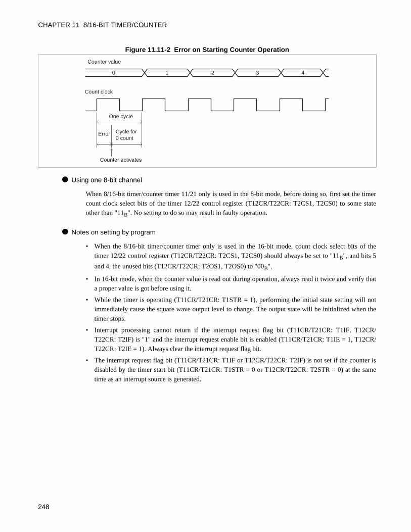
CHAPTER 11 8/16-BIT TIMER/COUNTER
Figure 11.11-2 Error on Starting Counter Operation
Using one 8-bit channel
When 8/16-bit timer/counter timer 11/21 only is used in the 8-bit mode, before doing so, first set the timer
count clock select bits of the timer 12/22 control register (T12CR/T22CR: T2CS1, T2CS0) to some state
other than "11B". No setting to do so may result in faulty operation.
Notes on setting by program
• When the 8/16-bit timer/counter timer only is used in the 16-bit mode, count clock select bits of the
timer 12/22 control register (T12CR/T22CR: T2CS1, T2CS0) should always be set to "11B", and bits 5
and 4, the unused bits (T12CR/T22CR: T2OS1, T2OS0) to "00B".
• In 16-bit mode, when the counter value is read out during operation, always read it twice and verify that
a proper value is got before using it.
• While the timer is operating (T11CR/T21CR: T1STR = 1), performing the initial state setting will not
immediately cause the square wave output level to change. The output state will be initialized when the
timer stops.
• Interrupt processing cannot return if the interrupt request flag bit (T11CR/T21CR: T1IF, T12CR/
T22CR: T2IF) is "1" and the interrupt request enable bit is enabled (T11CR/T21CR: T1IE = 1, T12CR/
T22CR: T2IE = 1). Always clear the interrupt request flag bit.
• The interrupt request flag bit (T11CR/T21CR: T1IF or T12CR/T22CR: T2IF) is not set if the counter is
disabled by the timer start bit (T11CR/T21CR: T1STR = 0 or T12CR/T22CR: T2STR = 0) at the same
time as an interrupt source is generated.
0 1 2 3 4
Count clock
One cycle
Error Cycle for0 count
Counter activates
Counter value
248

11.12 Program Examples for 8/16-bit Timer/Counter
This section gives a program examples for 8/16-bit timer/counter.
Program Example for Interval Timer Function
Processing description
• Using Timer ch.1 only, in 8-bit mode, generates interval timer interrupts at 20 ms intervals.
• Outputs a square wave to the TO1 pin that inverts after each interval time.
• With a main clock master oscillation FCH of 12.5 MHz, and the highest speed main clock selected by
the speed-shift function (1 instruction cycle time = 4/FCH), and with an internal clock period of 512 tinst
selected as the count clock, the T11DR setting for an interval of approximately 20 ms is calculated as
follows:
T11DR register value = 20 ms/(512 × 4/12.5 MHz) - 1 = 122.07 (7AH)
Coding example
T12CR EQU 003AH ; Address of the Timer 12 control register
T11CR EQU 003BH ; Address of the Timer 11 control register
T12DR EQU 003CH ; Address of the Timer 12 data register
T11DR EQU 003DH ; Address of the Timer 11 data register
T1IF EQU T11CR:7 ; Define the timer Ch1 interrupt request flag bit.
ILR2 EQU 007CH ;Address of the interrupt level setting register 2
INT_V DSEGABS
ORG0 FFEEH
IRQ6 DW WARI ;Set interrupt vector.
ENDS
;----------Main program-----------------------------------------------------------------------------------------------------
CSEG ;[CODE SEGMENT]
;Stack pointer (SP) etc. are already initialized.
:
CLRI ;Disable interrupts.
MOV ILR2,#11101111B ;Set interrupt priority to level 2.
MOV T12CR,#00000010B ;Clear timer 12 interrupt request flag, disable interrupt request
output, set other than 16-bit mode, stop operation.
MOV T11CR,#00011000B ; Clear timer 11 interrupt request flag, initialize
square wave output
249

CHAPTER 11 8/16-BIT TIMER/COUNTER
; "L", select 512 tinst, and stop operation.
MOV T11DR,#7AH ; Set value compared with the counter value (interval time).
MOV T11CR,#11111001B ; timer 11 interrupt request, clear counter, and start timer.
SETI ; Enable CPU interrupts.
:
:
;----------Interrupt Program-------------------------------------------------------------------------------------------------
WARI
CLRB T1IF ; Clear interrupt request flag.
PUSHW A
XCHW A,T
PUSHW A
:
User processing
:
POPW A
XCHW A,T
POPW A
RETI
ENDS
;--------------------------------------------------------------------------------------------------------------------------------
END
250

Program Example for Pulse Counter Function
Processing description
• Using Timer ch.1 in 16-bit mode, count external clocks input to the EC1 pin, and generate an interrupt
once for each 5000 clocks (1388H).
• Shows a sample program (READ16) for reading out the count in the 16-bit counter, while the counter is
counting.
Coding example
DDR2 EQU 0006H ; Address of the Port 2 direction register
T12CR EQU 003AH ; Address of the Timer 12 control register
T11CR EQU 003BH ; Address of the Timer 11 control register
T12DR EQU 003CH ; Address of the Timer 12 data register
T11DR EQU 003DH ; Address of the Timer 11 data register
T1IF EQU T11CR:7 ; Define the timer Ch1 interrupt request flag bit.
ILR2 EQU 007CH ; Address of the interrupt level setting register 3
NT_V DSEG ABS
ORG 0FFEEH
IRQ6 DW WARI ; Set interrupt vector.
ENDS
;----------Main program-----------------------------------------------------------------------------------------------------
CSEG ; [CODE SEGMENT]
; Stack pointer (SP) etc. are already initialized.
MOV DDR2,#00000000B ; Set EC pin as an input.
CLRI ; Disable interrupts.
MOV ILR2,#11101111B ; Set interrupt level 2.
MOV T11DR,#088H ; Set lower 8 bits of counter comparison value.
MOV T12DR,#013H ; Set upper 8 bits of counter comparison value.
MOV T12CR,#00001100B ; Set timer 12 to 16-bit mode.
MOV T11CR,#01001101B ; Clear timer 11 interrupt request flag, enable
interrupt request output, set P26/V1/TO1
as general-purpose port (P26), select external
clock, clear counter, and start operation.
SETI ; Enable CPU interrupts.
;----------Data read subroutine--------------------------------------------------------------------------------------
READ16
MOVW A,T12DR ; 16-bit read, T11DR + T12DR.
MOVW A,T12DR ; 16-bit read, T11DR + T12DR, save old value in T register.
CMPW A ; Check first and second reads, compare A and T registers.
BEQ RET16 ; If match, return.
251
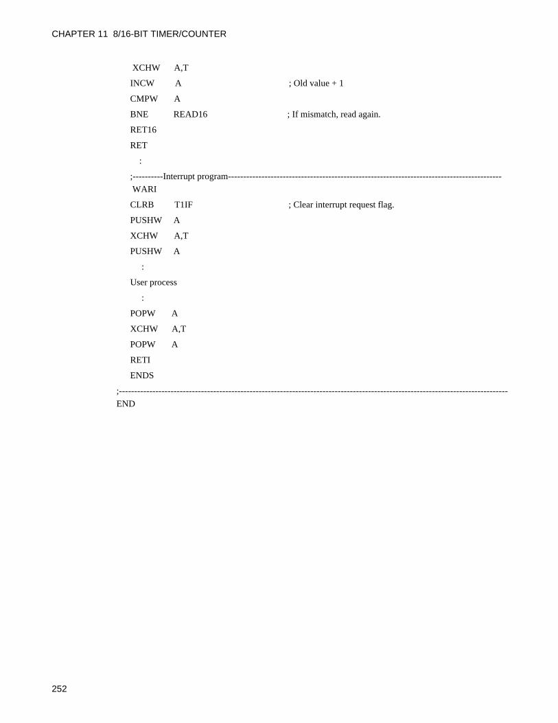
CHAPTER 11 8/16-BIT TIMER/COUNTER
XCHW A,T
INCW A ; Old value + 1
CMPW A
BNE READ16 ; If mismatch, read again.
RET16
RET
:
;----------Interrupt program------------------------------------------------------------------------------------------
WARI
CLRB T1IF ; Clear interrupt request flag.
PUSHW A
XCHW A,T
PUSHW A
:
User process
:
POPW A
XCHW A,T
POPW A
RETI
ENDS
;--------------------------------------------------------------------------------------------------------------------------------
END
252
CHAPTER 12EXTERNAL INTERRUPT 1
CIRCUIT (EDGE)
This chapter describes the functions and operation of the external interrupt 1 circuit (edge).
12.1 Overview of the External Interrupt 1 Circuit
12.2 Block Diagram of the External Interrupt 1 Circuit
12.3 Pins of the External Interrupt 1 Circuit
12.4 Registers of External Interrupt 1 Circuit
12.5 External Interrupt 1 Circuit Interrupts
12.6 Operation of the External Interrupt 1 Circuit
12.7 Program Example for the External Interrupt 1 Circuit
253

CHAPTER 12 EXTERNAL INTERRUPT 1 CIRCUIT (EDGE)
12.1 Overview of the External Interrupt 1 Circuit
The external interrupt 1 circuit detects edges on the signals input to the four external interrupt pins and generates the corresponding interrupt requests to the CPU.
Functions of the External Interrupt Circuit 1The function of the external interrupt 1 circuit is to detect specified edges on signals input to the external
interrupt pins and to generate interrupt requests to the CPU. These interrupts can cancel standby mode and
return the device to the normal operating state (main RUN state).
External interrupt pins: 4 pins (P10/SEG23/INT10 to P13/SEG26/INT13)
External interrupt sources: Input of a specified edge (rising edge or falling edge) on the signal input to an
external interrupt pin.
Interrupt control: Output of external interrupt requests is enabled or disabled by the interrupt
request enable bits in external interrupt control registers 1 and 2 (EIC1, EIC2).
Interrupt flags: Detection of specified edges sets the external interrupt request flag bits in
external interrupt control registers 1 and 2 (EIC1, EIC2).
Interrupt request: Separate interrupt requests are generated for each external interrupt source
(IRQ0, IRQ1, IRQ2, IRQ3).
254

12.2 Block Diagram of the External Interrupt 1 Circuit
The external interrupt 1 circuit consists of four blocks with the same functions.Each block contains the following two elements:• Edge detect circuits (10 to 13)• External interrupt control registers 1, 2 (EIC1, EIC2)
Block Diagram of the External Interrupt 1 Circuit
Figure 12.2-1 Block Diagram of the External Interrupt 1 Circuit
Edge detect circuit
If the polarity of an edge on the input signal to one of the external interrupt 1 circuit pins (INT10 to INT13)
matches the edge polarity specified for the pin in the EIC1 or EIC2 register (SEL0 to SEL7), the edge
detect circuit sets the corresponding external interrupt request flag bit (EIR0 to EIR3) to "1".
External interrupt control registers (EIC1, EIC2)
The EIC1 and EIC2 registers are used for operations such as edge selection, enabling or disabling interrupt
requests, and checking interrupt requests.
1
Sel
ecto
r
EIC1
P11/SEG24/INT11
IRQ0
Edge detect circuit 11
Pin
EIR1 SEL3 SEL2 EIE1
2
3
1
Sel
ecto
r
EIC1
P10/SEG23/INT10
Edge detect circuit 10
Pin
EIR0 SEL1 SEL0 EIE0
2
3
1
Sel
ecto
r
EIC2
P13/SEG26/INT13
Edge detect circuit 13
Pin
EIR3 SEL7 SEL6 EIE3
2
3
1
Sel
ecto
r
EIC2
P12/SEG25/INT12
IRQ1
Edge detect circuit 12
Pin
EIR2 SEL5 SEL4 EIE2
2
3
IRQ2IRQ3
255

CHAPTER 12 EXTERNAL INTERRUPT 1 CIRCUIT (EDGE)
12.3 Pins of the External Interrupt 1 Circuit
This section describes the pins, pin block diagram, registers, and external interrupt sources of the external interrupt 1 circuit.
Pins of External Interrupt 1 CircuitThe external interrupt 1 circuit has four external interrupt pins. The external interrupt pins can function
either as external interrupt inputs (hysteresis inputs) or general-purpose I/O ports.
Although the P10/SEG23/INT10 to P13/SEG26/INT13 pins continuously function as external interrupt
input, the external interrupt 1 circuit does not output interrupt requests if output of interrupt requests is
disabled for the pin. The pin states can be read directly from the port data register (PDR1) at any time.
INT10 to INT13: The external interrupt 1 circuit generates the interrupt request for the pin when an edge of
the specified polarity is input.
Block Diagram of the External Interrupt 1 Circuit Pins
Figure 12.3-1 Block Diagram of the External Interrupt 1 Circuit Pins
Table 12.3-1 Pins of External Interrupt 1 Circuit
External Interrupt PinWhen Used as an External
Interrupt Input (Output of Interrupt Requests Enabled)
When Used as an Input-Only Port (Output of Interrupt Requests
Disabled)
P10/SEG23/INT10 INT10 (EIC1: EIE0=1) P10 (EIC1: EIE0=0)
P11/SEG24/INT11 INT11 (EIC1: EIE1=1) P11 (EIC1: EIE1=0)
P12/SEG25/INT12 INT12 (EIC2: EIE2=1) P12 (EIC2: EIE2=0)
P13/SEG26/INT13 INT13 (EIC2: EIE3=1) P13 (EIC2: EIE3=0)
PDR (Port data register)
DDR
Inte
rnal
dat
a bu
s
PDR read
PDR read (for bit manipulation instructions)
PDR write
DDR write (Port direction register)
Pin
SPL: Pin state specification bit in the standby control register (STBC)
N-ch
Stop, watch mode (SPL = 1)
Output latch
External interrupt input enable
To external interrupt input
LCD output enable
Stop, watch mode
P10/SEG23/INT10P11/SEG24/INT11P12/SEG25/INT12P13/SEG26/INT13
256

12.4 Registers of External Interrupt 1 Circuit
This section describes the registers of the external interrupt 1 circuit.
Figure 12.4-1 Registers of External Interrupt 1 Circuit
External Interrupt 1 Circuit Interrupt SourcesIRQ0: This interrupt request is generated if an edge of the selected polarity is input to the external
interrupt 1 circuit pin INT10 when output of interrupt requests is enabled.
IRQ1: This interrupt request is generated if an edge of the selected polarity is input to the external
interrupt 1 circuit pin INT11 when output of interrupt requests is enabled.
IRQ2: This interrupt request is generated if an edge of the selected polarity is input to the external
interrupt 1 circuit pin INT12 when output of interrupt requests is enabled.
IRQ3: This interrupt request is generated if an edge of the selected polarity is input to the external
interrupt 1 circuit pin INT13 when output of interrupt requests is enabled.
EIC1 (External interrupt control register 1)
EIC2 (External interrupt control register 2)
Address bit7 bit6 bit5 bit4 bit3 bit2 bit1 bit0 Initial value
0025H EIR1 SEL3 SEL2 EIE1 EIR0 SEL1 SEL0 EIE0 00000000B
R/W R/W R/W R/W R/W R/W R/W R/W
Address bit7 bit6 bit5 bit4 bit3 bit2 bit1 bit0 Initial value
0026H EIR3 SEL7 SEL6 EIE3 EIR2 SEL5 SEL4 EIE2 00000000B
R/W R/W R/W R/W R/W R/W R/W R/W
R/W : Readable /Writable
IRQ1INT11
IRQ0INT10
IRQ2INT12
IRQ3INT13
257

CHAPTER 12 EXTERNAL INTERRUPT 1 CIRCUIT (EDGE)
12.4.1 External Interrupt Control Register 1 (EIC1)
External interrupt control register 1 (EIC1) is used to select the edge polarity and to control interrupts for external interrupt pins INT10, INT11.
External Interrupt Control Register 1 (EIC1)
Figure 12.4-2 External Interrupt Control Register 1 (EIC1)
Address bit7 bit6 bit5 bit4 bit3 bit2 bit1 bit0 Initial value
0025H EIR1 SEL3 SEL2 EIE1 EIR0 SEL1 SEL0 EIE0 00000000B
R/W R/W R/W R/W R/W R/W R/W R/W
EIE0 INT10 Interrupt request enable bit0 Disable output of interrupt requests.1 Enable output of interrupt requests.
SEL1 SEL0 INT10 Edge polarity selection bits0 0 No edge detection0 1 Rising edge1 0 Falling edge1 1 Both edges
EIR0INT10 External interrupt request flag bit
Read Write
0 The specified edge has not been input. Clear this bit.
1 The specified edge has been input. No effect. The bit does not change.
EIE1 INT11 Interrupt request enable bit0 Disable output of interrupt requests.1 Enable output of interrupt requests.
SEL3 SEL2 INT11 Edge polarity selection bits0 0 No edge detection0 1 Rising edge1 0 Falling edge1 1 Both edges
EIR1INT11 External interrupt request flag bit
Read Write0 The specified edge has not been input. Clear this bit.1 The specified edge has been input. No effect. The bit does not change.
R/W : Readable/Writable: Initial value
258

Table 12.4-1 External Interrupt Control Register 1 (EIC1) Bits
Bit name Function
bit7EIR1: INT11External interrupt request flag bit
• This bit is set to "1" when the edge selected by INT11 edge polarity selection bits (SEL3, SEL2) is input to external interrupt pin INT11.
• An interrupt request is output when both this bit and INT11 interrupt request enable bit (EIE1) are "1".
• Writing "0" clears the bit. Writing "1" has no effect and does not change the bit value.
bit6,bit5
SEL3, SEL2: INT11Edge polarity selection bits
• Control the mode of the input edge polarity of INT11 pin• Writing "00" uses no edge detection, "01" uses rising-edge mode, "10" uses falling-
edge mode or "11" uses both-edge mode. • Always write "0" into EIR1 when changing this bit.
bit4EIE1: INT11Interrupt request enable bit
Enables or disables output of interrupt requests to the CPU. An interrupt request is output when both this bit and INT11 external interrupt request flag bit (EIR1) are "1".
bit3EIR0: INT10External interrupt request flag bit
• This bit is set to "1" when the edge selected by INT10 edge polarity selection bits (SEL1, SEL0) is input to external interrupt pin INT10.
• An interrupt request is output when both this bit and INT10 interrupt request enable bit (EIE0) are "1".
• Writing "0" clears the bit. Writing "1" has no effect and does not change the bit value.
bit2,bit1
SEL1, SEL0: INT10Edge polarity selection bits
• Control the mode of the input edge polarity of INT10 pin• Writing "00" uses no edge detection, "01" uses rising-edge mode, "10" uses falling-
edge mode or "11" uses both-edge mode. • Always write "0" into EIR0 when changing this bit.
bit0EIE0: INT10Interrupt request enable bit
Enables or disables output of interrupt requests to the CPU. An interrupt request is output when both this bit and INT10 external interrupt request flag bit EIR0) are "1".
259

CHAPTER 12 EXTERNAL INTERRUPT 1 CIRCUIT (EDGE)
12.4.2 External Interrupt Control Register 2 (EIC2)
External interrupt control register 2 (EIC2) is used to select the edge polarity and to control interrupts for external interrupt pins INT12, INT13.
External Interrupt Control Register 2 (EIC2)
Figure 12.4-3 External Interrupt Control Register 2 (EIC2)
Address bit7 bit6 bit5 bit4 bit3 bit2 bit1 bit0 Initial value
0026H EIR3 SEL7 SEL6 EIE3 EIR2 SEL5 SEL4 EIE2 00000000B
R/W R/W R/W R/W R/W R/W R/W R/W
EIE2 INT12 Interrupt request enable bit0 Disable output of interrupt requests.
1 Enable output of interrupt requests.
SEL5 SEL4 INT12 Edge polarity selection bits0 0 No edge detection0 1 Rising edge1 0 Falling edge1 1 Both edges
EIR2INT12 External interrupt request flag bit
Read Write
0 The specified edge has not been input. Clear this bit.
1 The specified edge has been input. No effect. The bit does not change.
EIE3 INT13 Interrupt request enable bit0 Disable output of interrupt requests.1 Enable output of interrupt requests.
SEL7 SEL6 INT 13 Edge polarity selection bits
0 0 No edge detection0 1 Rising edge1 0 Falling edge1 1 Both edges
EIR3INT13 External interrupt request flag bit
Read Write
0 The specified edge has not been input. Clear this bit.
1 The specified edge has been input. No effect. The bit does not change.R/W : Readable/Writable
: Initial value
260

Table 12.4-2 External Interrupt Control Register 2 (EIC2) Bits
Bit name Function
bit7EIR3: INT13External interrupt request flag bit
• This bit is set to "1" when the edge selected by INT13 edge polarity selection bits (SEL7, SEL6) is input to external interrupt pin INT13.
• An interrupt request is output when both this bit and INT13 interrupt request enable bit (EIE3) are "1".
• Writing "0" clears the bit. Writing "1" has no effect and does not change the bit value.
bit6,bit5
SEL7, SEL6: INT13Edge polarity selection bits
• Control the mode of the input edge polarity of INT13 pin• Writing "00" uses no edge detection, "01" uses rising-edge mode, "10" uses falling-
edge mode or "11" uses both-edge mode. • Always write "0" into EIR3 when changing this bit.
bit4EIE3: INT13Interrupt request enable bit
Enables or disables output of interrupt requests to the CPU. An interrupt request is output when both this bit and INT13 external interrupt request flag bit (EIR3) are "1".
bit3EIR2: INT12External interrupt request flag bit
• This bit is set to "1" when the edge selected by INT12 edge polarity selection bits (SEL5, SEL4) is input to external interrupt pin INT12.
• An interrupt request is output when both this bit and INT12 interrupt request enable bit (EIE2) are "1".
• Writing "0" clears the bit. Writing "1" has no effect and does not change the bit value.
bit2,bit1
SEL5, SEL4: INT12Edge polarity selection bits
• Control the mode of the input edge polarity of INT12 pin• Writing "00" use no edge detection, "01" uses rising-edge mode, "10" uses falling-
edge mode or "11" uses both-edge mode. • Always write "0" into EIR2 when changing this bit.
bit0EIE2: INT12Interrupt request enable bit
Enables or disables output of interrupt requests to the CPU. An interrupt request is output when both this bit and INT12 external interrupt request flag bit (EIR2) are "1".
261

CHAPTER 12 EXTERNAL INTERRUPT 1 CIRCUIT (EDGE)
12.5 External Interrupt 1 Circuit Interrupts
The external interrupt 1 circuit can generate interrupt requests when it detects a specified edge on the signal input to an external interrupt pin.
Interrupts When the External Interrupt Circuit 1 is OperatingOn detecting a specified edge on an external interrupt input, the external interrupt circuit sets the
corresponding external interrupt request flag bit (EIC1, EIC2 : EIR0 to EIR3) to "1". An interrupt request
to the CPU (IRQ0 to IRQ3) is generated at this time if the corresponding interrupt request enable bit is
enabled (EIC1, EIC2,: EIE0 to EIE3 = 1). Always write "0" to the corresponding external interrupt request
flag bit in the interrupt processing routine to clear the interrupt request.
Notes:
• When enabling interrupts (EIE0 to EIE3 = 1) after exit of a reset, always clear the correspondingexternal interrupt request flag bit (EIR0 to EIR3 = 0) at the same time.Interrupt processing cannot return if the external interrupt request flag bit is "1" and the interruptrequest enable bit is enabled. Always clear the external interrupt request flag bit in the interruptprocessing routine.
• Cancelling stop mode using an interrupt is only possible using the external interrupt circuit.An interrupt request is generated immediately if the external interrupt request flag bit is "1" whenthe interrupt request enable bit is changed from disabled to enabled ("0" -> "1").
Register and Vector Table for the External Interrupt 1 Circuit Interrupts
Reference:
See "3.4.2 Interrupt Processing" for details on the operation of interrupts.
Notes when changing edge polarity selectionWhen changing the edge polarity for INT10 to INT13, always write "0" into the corresponding EIR bits.
This will prevent accidentally creating an interrupt.
Table 12.5-1 Register and Vector Table for External Interrupt 1 Circuit Interrupts
InterruptInterrupt Level Setting Register Vector Table Address
Register Setting Bits Upper Lower
IRQ0 ILR1 (007BH) L01 (bit1) L00 (bit0) FFFAH FFFBH
IRQ1 ILR1 (007BH) L11 (bit3) L10 (bit2) FFF8H FFF9H
IRQ2 ILR1 (007BH) L21 (bit5) L20 (bit4) FFF6H FFF7H
IRQ3 ILR1 (007BH) L31 (bit7) L30 (bit6) FFF4H FFF5H
262
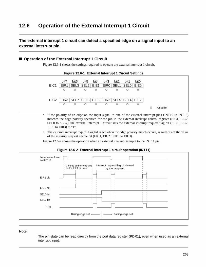
12.6 Operation of the External Interrupt 1 Circuit
The external interrupt 1 circuit can detect a specified edge on a signal input to an external interrupt pin.
Operation of the External Interrupt 1 CircuitFigure 12.6-1 shows the settings required to operate the external interrupt 1 circuit.
Figure 12.6-1 External Interrupt 1 Circuit Settings
• If the polarity of an edge on the input signal to one of the external interrupt pins (INT10 to INT13)matches the edge polarity specified for the pin in the external interrupt control register (EIC1, EIC2:SEL0 to SEL7), the external interrupt 1 circuit sets the external interrupt request flag bit (EIC1, EIC2:EIR0 to EIR3) to "1".
• The external interrupt request flag bit is set when the edge polarity match occurs, regardless of the valueof the interrupt request enable bit (EIC1, EIC2 : EIE0 to EIE3).
Figure 12.6-2 shows the operation when an external interrupt is input to the INT11 pin.
Figure 12.6-2 External interrupt 1 circuit operation (INT11)
Note:
The pin state can be read directly from the port data register (PDR1), even when used as an externalinterrupt input.
bit7 bit6 bit5 bit4 bit3 bit2 bit1 bit0EIC1 EIR1 SEL3 SEL2 EIE1 EIR0 SEL1 SEL0 EIE0
EIC2 EIR3 SEL7 SEL6 EIE3 EIR2 SEL5 SEL4 EIE2
: Used bit
Cleared at the same time as the EIE1 bit is set.
Interrupt request flag bit cleared by the program.
EIR1 bit
EIE1 bit
SEL3 bit
Rising edge set Falling edge set
IRQ1
SEL2 bit
Input wave formto INT 11
263

CHAPTER 12 EXTERNAL INTERRUPT 1 CIRCUIT (EDGE)
12.7 Program Example for the External Interrupt 1 Circuit
This section gives a program example for the external interrupt 1 circuit.
Program Example for the External Interrupt 1 Circuit
Processing description
Generates interrupts on detecting a rising edge on pulses input to the INT11 pin.
Coding example
EIC1 EQU 0025H ;External interrupt control register 1
EIR1 EQU EIC1:7 ;Defines the external interrupt request flag bit.SEL2 EQU EIC1:5 ;Defines the edge polarity selection bit.EIE1 EQU EIC1:4 ;Defines the interrupt request enable bit.
ILR0 EQU 007BH ;Set interrupt level setting register 1.
INT_V DSEG ABS ;[DATA SEGMENT]ORG 0FFF8H
IRQ1 DW WARI ;Set INT11 interrupt vector.INT_V ENDS;-----Main program----------------------------------------------------------------------------------------------------------------------------
CSEG ;[CODE SEGMENT];Stack pointer (SP) etc. are already initialized.
:CLRI ;Disable interrupts.CLRB EIR1 ;Clear interrupt request flag.MOV ILR0,#11110111B ;Set interrupt level (level 1).SETB SEL2 ;Select rising edge.SETB EIE1 ;Enable output of interrupt requests.SETI ;Enable interrupts.
:;-----Interrupt processing routine------------------------------------------------------------------------------------------------------------WARI CLRB EIR1 ;Clear INT11 interrupt request flag.
PUSHW AXCHW A,TPUSHW A
:User processing
:POPW AXCHW A,TPOPW ARETIENDS
;---------------------------------------------------------------------------------------------------------------------------------------------------END
264

CHAPTER 13EXTERNAL INTERRUPT 2
CIRCUIT (LEVEL)
This chapter describes the functions and operation of the external interrupt 2 circuit (level).
13.1 Overview of External Interrupt 2 Circuit (Level)
13.2 Block Diagram of External Interrupt 2 Circuit
13.3 Pins of External Interrupt 2 Circuit
13.4 Registers of External Interrupt 2 Circuit
13.5 External Interrupt 2 Circuit Interrupt
13.6 Operation of External Interrupt 2 Circuit
13.7 Program Example for External Interrupt 2 Circuit
265
CHAPTER 13 EXTERNAL INTERRUPT 2 CIRCUIT (LEVEL)
13.1 Overview of External Interrupt 2 Circuit (Level)
The external interrupt circuit 2 detects the level of the signals input to the eight external interrupt pins and generates the interrupt requests to the CPU.
External Interrupt 2 Circuit Function (Level Detection)The external interrupt 2 circuit function detects the signals of the "L" levels input to the external interrupt
pins and to generate interrupt request to the CPU. These interrupts can wake up the CPU from standby
mode and change the device to the normal operating state (main-run or sub-run mode).
External interrupt pins: 8 pins (P00/INT20 to P07/INT27/BUZ)
External interrupt sources: "L" level signal input to an external interrupt pin.
Interrupt control: Enables or disables to input external interrupt controlled by external
interrupt 2 control register (EIE2)
Interrupt flag: IRQ flag bit of external interrupt 2 flag register (EIF2). Flag set when there
is an IRQ.
Interrupt request: IRQ4 is generated if any enabled external interrupt pin is "L".
266
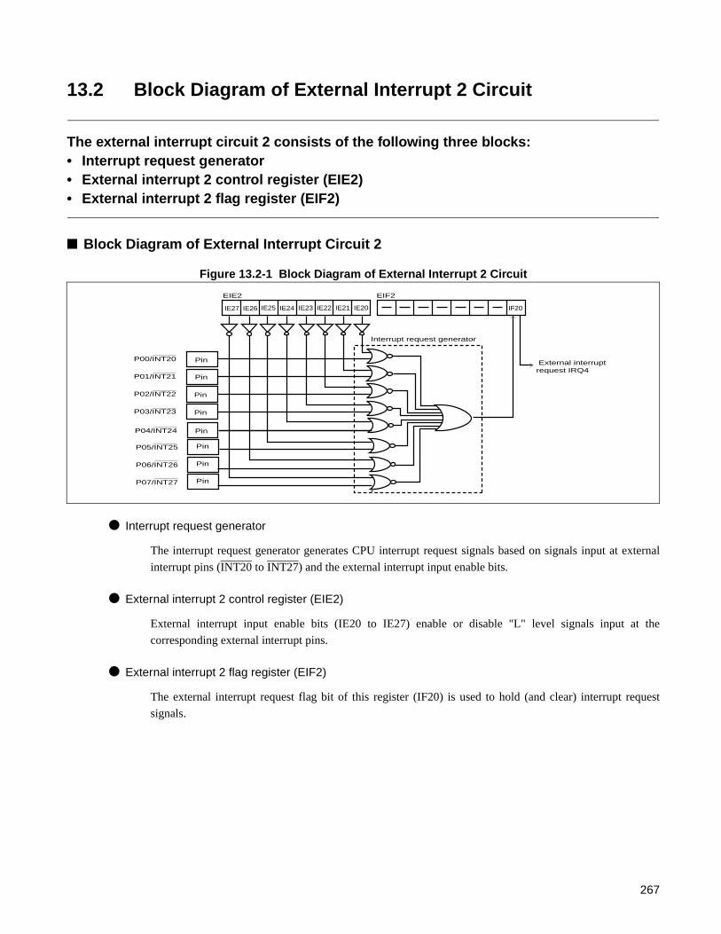
13.2 Block Diagram of External Interrupt 2 Circuit
The external interrupt circuit 2 consists of the following three blocks:• Interrupt request generator• External interrupt 2 control register (EIE2)• External interrupt 2 flag register (EIF2)
Block Diagram of External Interrupt Circuit 2
Figure 13.2-1 Block Diagram of External Interrupt 2 Circuit
Interrupt request generator
The interrupt request generator generates CPU interrupt request signals based on signals input at external
interrupt pins (INT20 to INT27) and the external interrupt input enable bits.
External interrupt 2 control register (EIE2)
External interrupt input enable bits (IE20 to IE27) enable or disable "L" level signals input at the
corresponding external interrupt pins.
External interrupt 2 flag register (EIF2)
The external interrupt request flag bit of this register (IF20) is used to hold (and clear) interrupt request
signals.
P00/INT20
P01/INT21
P02/INT22
P03/INT23
EIE2 EIF2
IE23 IE22 IE21 IE20 IF20
Pin
Pin
Pin
Pin
Interrupt request generator
External interrupt request IRQ4
PinP04/INT24
IE24
Pin
Pin
Pin
P05/INT25
P06/INT26
P07/INT27
IE25IE26IE27
267

CHAPTER 13 EXTERNAL INTERRUPT 2 CIRCUIT (LEVEL)
13.3 Pins of External Interrupt 2 Circuit
This section describes the pins, pin block diagram, registers, and external interrupt sources of the external interrupt 2 circuit.
Pins of External Interrupt 2 CircuitThe external interrupt 2 circuit uses eight external interrupt pins.
The external interrupt pins can function either as external interrupt inputs (hysteresis inputs) or as general-
purpose or peripheral I/O pin.
When P00/INT20 to P07/INT27/BUZ pins are set as inputs in the port 0 direction register (DDR0), and the
corresponding external interrupt inputs are enabled in the external interrupt 2 control register (EIE2), they
operate as external interrupt input pins (INT20 to INT27). When they are being used as the input port, the
pin states can be read from the port data register (PDR0) at any time.
Table 13.3-1 lists the pins of external interrupt 2 circuit.
Table 13.3-1 Pins of External Interrupt 2 Circuit
External interrupt pinWhen used as an external interrupt input
(Interrupt Input Enabled)
When used as General-purpose I/O port or other pheripheral I/O
(Interrupt Input Disabled)
P00/INT20 INT20 (EIE2:IE20=1) P00 (EIE2:IE20=0)
P01/INT21 INT21 (EIE2:IE21=1) P01 (EIE2:IE21=0)
P02/INT22 INT22 (EIE2:IE22=1) P02 (EIE2:IE22=0)
P03/INT23 INT23 (EIE2:IE23=1) P03 (EIE2:IE23=0)
P04/INT24 INT24 (EIE2:IE24=1) P04 (EIE2:IE24=0)
P05/INT25/PWC INT25 (EIE2:IE25=1) P05/PWC (EIE2:IE25=0)
P06/INT26/PPG INT26 (EIE2:IE26=1) P06/PPG (EIE2:IE26=0)
P07/INT27/BUZ INT27 (EIE2:IE27=1) P07/BUZ (EIE2:IE27=0)
268

Block Diagram of External Interrupt 2 Circuit Pins
Figure 13.3-1 Block Diagram of External Interrupt 2 Circuit Pins
Note:
Pins with a pull-up resistor go to the "H" level (pull-up state) rather than the high-impedance statewhen the output transistor is turned "OFF". However, during reset, pull-up is unavailable and will beHi-Z.
DDR
Inte
rnal
dat
a bu
s
PDR read
PDR read (for bit manipulation instructions)
PDR write
Pull-up resistorApprox. 50 kΩ
Pins
SPL: Pin state specification bit in the standby control register (STBC)
N-ch
P-ch
P-ch
Stop, watch mode
Output latch
To external interrupt circuit External interrupt input enable
Stop, watch mode
DDR write (Port direction register)
Pull-up resistor control register
PDR (Port data register)
(SPL = 1)
P00/INT20P01/INT21P02/ITN22P03/INT23P04/INT24
P05/INT25/PWCP06/INT26/PPGP07/INT27/BUZ
269

CHAPTER 13 EXTERNAL INTERRUPT 2 CIRCUIT (LEVEL)
13.4 Registers of External Interrupt 2 Circuit
This section describes the registers of the external interrupt 2 circuit.
Figure 13.4-1 Registers of External Interrupt 2 Circuit
External Interrupt 2 Circuit Interrupt SourcesIRQ4:
IRQ4 is generated if any one of external interrupt pins INT20 to INT27 are input "L" level signal with "1"
in the external interrupt input enable bit for that pin.
EIE2 (External interrupt 2 control register)
EIF2 (External interrupt 2 flag register)
Address bit7 bit6 bit5 bit4 bit3 bit2 bit1 bit0 Initial value
0027H IE27 IE26 IE25 IE24 IE23 IE22 IE21 IE20 00000000B
R/W R/W R/W R/W R/W R/W R/W R/W
Address bit7 bit6 bit5 bit4 bit3 bit2 bit1 bit0 Initial value
0028H — — — — — — — IF20 -------0B
R/WR/W : Readable/Writable— : Undefined
270

13.4.1 External Interrupt 2 Control Register (EIE2)
The external interrupt 2 control register (EIE2) is used to enable/disable input of external interrupt pins (INT20 to INT27).
External Interrupt 2 Control Register (EIE2)
Figure 13.4-2 External Interrupt 2 Control Register (EIE2)
Address bit7 bit6 bit5 bit4 bit3 bit2 bit1 bit0 Initial value
0027H IE27 IE26 IE25 IE24 IE23 IE22 IE21 IE20 00000000B
R/W R/W R/W R/W R/W R/W R/W R/W
IE20 to
IE27External interrupt input enable bits
0 Enables external interrupt input
1 Disables external interrupt input
R/W : Readable/Writable— : Undefined
: Initial value
Table 13.4-1 External Interrupt 2 Control Register (EIE2) Bits vs. Pins
Bit Pin
bit 7 IE27 INT27
bit 6 IE26 INT26
bit 5 IE25 INT25
bit 4 IE24 INT24
bit 3 IE23 INT23
bit 2 IE22 INT22
bit 1 IE21 INT21
bit 0 IE20 INT20
271
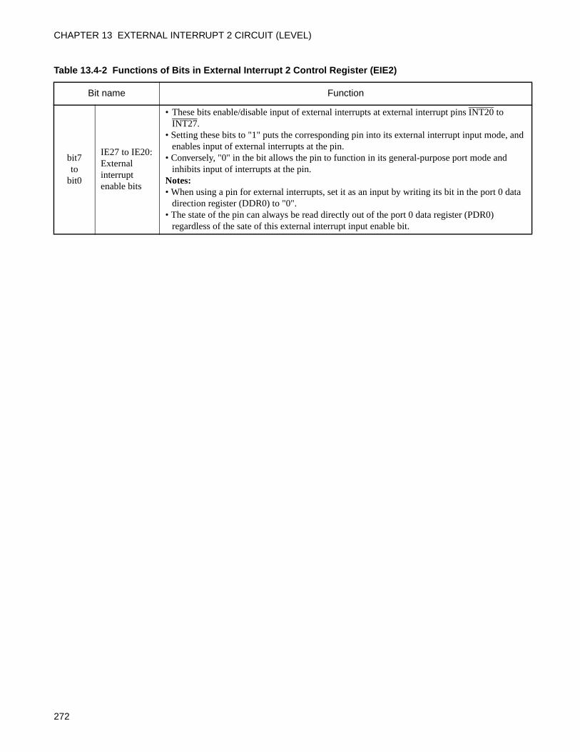
CHAPTER 13 EXTERNAL INTERRUPT 2 CIRCUIT (LEVEL)
Table 13.4-2 Functions of Bits in External Interrupt 2 Control Register (EIE2)
Bit name Function
bit7to
bit0
IE27 to IE20:External interrupt enable bits
• These bits enable/disable input of external interrupts at external interrupt pins INT20 to INT27.
• Setting these bits to "1" puts the corresponding pin into its external interrupt input mode, and enables input of external interrupts at the pin.
• Conversely, "0" in the bit allows the pin to function in its general-purpose port mode and inhibits input of interrupts at the pin.
Notes:• When using a pin for external interrupts, set it as an input by writing its bit in the port 0 data
direction register (DDR0) to "0".• The state of the pin can always be read directly out of the port 0 data register (PDR0)
regardless of the sate of this external interrupt input enable bit.
272

13.4.2 External Interrupt 2 Flag Register (EIF2)
External Interrupt 2 flag register (EIF2) is used to hold the IRQ state when a level interrupt has been detected, and clear the interrupt request flag.
External Interrupt 2 Flag Register (EIF2)
Figure 13.4-3 External Interrupt 2 Flag Register (EIF2)
Address bit7 bit6 bit5 bit4 bit3 bit2 bit1 bit0 Initial value
0028H — — — — — — — IF20 --------0B
R/W
IF20 External interrupt request flag bit
Read Write
0 No external IRQ ("L" level not detected). Clears this bit.
1 Have external IRQ ("L" level detected).No effect. This bit does
not change.
R/W : Readable/Writable— : Undefined
: Initial value
Table 13.4-3 Functions of Bits in External Interrupt 2 Flag Register (EIF2)
Bit name Function
bit7to
bit1Undefined bits
• The read value is undefined.• Writing to these bits has no effect on the operation.
bit0IF20:External interrupt request flag bit
• This bit is set to "1" when a "L" is detected at an enabled external interrupt pin (INT20 to INT27).
• Writing "0" clears this bit. Writing "1" has no effect and does not change the bit value.Note:
Writing "0" to the external interrupt input enable bits of the external interrupt 2 control register (EIE2: IE20 to IE27) simply disables the corresponding external interrupt input; it does not clear the interrupt request. IRQ4 will continue to be sent to the CPU until it is cleared by writing "0" to the IF20 bit.
273
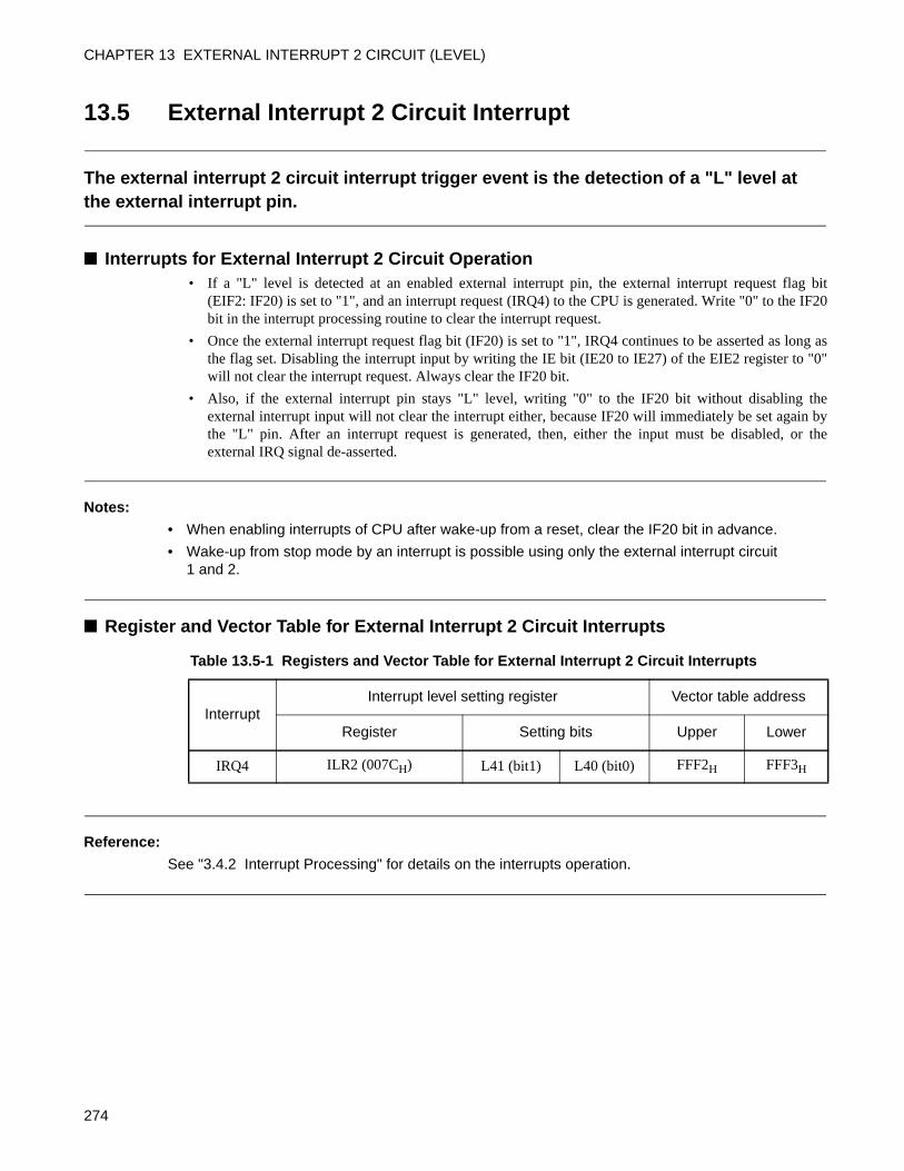
CHAPTER 13 EXTERNAL INTERRUPT 2 CIRCUIT (LEVEL)
13.5 External Interrupt 2 Circuit Interrupt
The external interrupt 2 circuit interrupt trigger event is the detection of a "L" level at the external interrupt pin.
Interrupts for External Interrupt 2 Circuit Operation• If a "L" level is detected at an enabled external interrupt pin, the external interrupt request flag bit
(EIF2: IF20) is set to "1", and an interrupt request (IRQ4) to the CPU is generated. Write "0" to the IF20bit in the interrupt processing routine to clear the interrupt request.
• Once the external interrupt request flag bit (IF20) is set to "1", IRQ4 continues to be asserted as long asthe flag set. Disabling the interrupt input by writing the IE bit (IE20 to IE27) of the EIE2 register to "0"will not clear the interrupt request. Always clear the IF20 bit.
• Also, if the external interrupt pin stays "L" level, writing "0" to the IF20 bit without disabling theexternal interrupt input will not clear the interrupt either, because IF20 will immediately be set again bythe "L" pin. After an interrupt request is generated, then, either the input must be disabled, or theexternal IRQ signal de-asserted.
Notes:
• When enabling interrupts of CPU after wake-up from a reset, clear the IF20 bit in advance.
• Wake-up from stop mode by an interrupt is possible using only the external interrupt circuit 1 and 2.
Register and Vector Table for External Interrupt 2 Circuit Interrupts
Reference:
See "3.4.2 Interrupt Processing" for details on the interrupts operation.
Table 13.5-1 Registers and Vector Table for External Interrupt 2 Circuit Interrupts
InterruptInterrupt level setting register Vector table address
Register Setting bits Upper Lower
IRQ4 ILR2 (007CH) L41 (bit1) L40 (bit0) FFF2H FFF3H
274

13.6 Operation of External Interrupt 2 Circuit
The external interrupt 2 circuit issues an interrupt request to the CPU when it detects a "L" level at one of its external interrupt pins.
Operation of External Interrupt 2 CircuitFigure 13.6-1 shows the settings required to operate the external interrupt 2 circuit.
Figure 13.6-1 External Interrupt 2 Circuit Settings
If a "L" level signal is applied to one of the INT20 to INT27 pins with the corresponding external interrupt
input enable bit (IE20 to IE27) in the "enable" state, the circuit sends an IRQ4 interrupt request to the CPU.
Figure 13.6-2 shows external interrupt 2 circuit operation (for a signal received at INT20).
Figure 13.6-2 Operation of External Interrupt 2 (INT20)
Note:
The pin state can be read directly from the port data register (PDR0) even when the pin is beingused as an external interrupt input.
bit7 bit6 bit5 bit4 bit3 bit2 bit1 bit0
EIE2 IE27 IE26 IE25 IE24 IE23 IE22 IE21 IE20
EIF2 — — — — — — — IF20
DDR0 — — — — — — — —
* * * * * * * *
: Used bit∗ : Set bits for pins used for external interrupts to "0"
RETIRETI
EIE2: IE20
PDR0: bit0
Input waveform to the INT20 pin ("L" level detected)
External interrupt input enabled
EIF2: IF20 (Same as IRQ4)
Cleared by the interrupt processing routine.
IRQ4 interrupt processing routine operation
Interrupt processing Interrupt processing
Can be read at any time.
275

CHAPTER 13 EXTERNAL INTERRUPT 2 CIRCUIT (LEVEL)
13.7 Program Example for External Interrupt 2 Circuit
This section gives a program example for the external interrupt 2 circuit.
Program Example for External Interrupt 2 Circuit
Processing description
Generates interrupts on detecting a "L" level input the INT20 pin.
Coding example
DDR0 EQU 0001H ; Address of port 0 data direction register EIE2 EQU 0027H ; Address of external interrupt 2 control register EIF2 EQU 0028H ; Address of external interrupt 2 flag register
IF20 EQU EIF2:0 ; Define the external interrupt request flag bit.
ILR2 EQU 007CH ; Address of the set interrupt level setting register 2
INT_V DSEG ABS ; [DATA SEGMENT] ORG 0FFF2H IRQ4 DW WARI ; Set interrupt vector. INT_V ENDS CSEG ;
CSEG ; [CODE SEGMENT] : ;Stack pointer (SP) etc. are already initialized. CLRI ; Disable interrupts. CLRB IF20 ; Clear external interrupt request flag. MOV ILR2,#11111110B ; Set interrupt priority (level 2). MOV DDR0,#00000000B ; Set P00/INT20 pin as input. MOV EIE2,#00000001B ; Enable external interrupt input at INT20 pin. SETI ; Enable interrupts.
WARI MOV EIE2,#00000000B ; Disable external interrupt input at INT20 pin. CLRB IF20 ; Clear external interrupt request flag. PUSHW A XCHW A,T PUSHW A : User processing : POPW A XCHW A,T POPW A RETI ENDS
END
;-------------------------------------------------------------------------------------------------------------------------------------Main program
;------------------------------------------------------------------------------------------------------------------------------------Interrupt processing routine
;------------------------------------------------------------------------------------------------------------------------------------
276

CHAPTER 14A/D CONVERTER
This chapter describes the functions and operation of the A/D converter.
14.1 Overview of A/D Converter
14.2 Block Diagram of A/D Converter
14.3 Pins of A/D Converter
14.4 Registers of A/D Converter
14.5 A/D Converter Interrupt
14.6 Operation of A/D Converter
14.7 Notes on Using A/D Converter
14.8 Program Example for A/D Converter
277
CHAPTER 14 A/D CONVERTER
14.1 Overview of A/D Converter
The A/D converter can function as an 10-bit successive approximation type A/D converter. The function selects one input signal from the four channels of analog input pin and can be activated either by software, by an internal clock, or by 8/16-bit timer 21 output.
A/D Conversion FunctionThe A/D conversion function converts the analog voltage (input voltage) input to an analog input pin to an
10-bit digital value.
• Selects one input from four analog input pins.
• Conversion speed is 60 instruction cycles (19.2 µs for a 12.5 MHz main clock source oscillation).
• Generates an interrupt when A/D conversion completes.
• Conversion completion can also be determined by software.
The following methods are available to activate A/D conversion:
• Activation by software
• Continuous activation by a time-base timer output (divide-by-28 main clock source oscillation)
• Continuous activation by 8/16-bit timer 21 output.
278
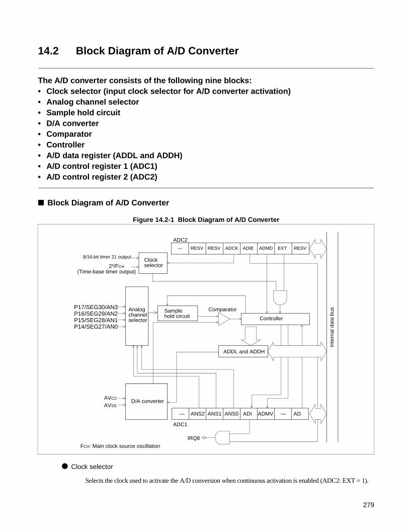
14.2 Block Diagram of A/D Converter
The A/D converter consists of the following nine blocks:• Clock selector (input clock selector for A/D converter activation)• Analog channel selector• Sample hold circuit• D/A converter• Comparator• Controller• A/D data register (ADDL and ADDH)• A/D control register 1 (ADC1)• A/D control register 2 (ADC2)
Block Diagram of A/D Converter
Figure 14.2-1 Block Diagram of A/D Converter
Clock selector
Selects the clock used to activate the A/D conversion when continuous activation is enabled (ADC2: EXT = 1).
ADC2
Inte
rnal
dat
a bu
s
ADC1
28/FCH
P17/SEG30/AN3P16/SEG29/AN2P15/SEG28/AN1P14/SEG27/AN0
AVCC
AVSS
Clock selector
Analog channel selector
Sample hold circuit
Comparator
Controller
ADDL and ADDH
D/A converter
FCH: Main clock source oscillation
IRQ8
(Time-base timer output)
— RESV RESV ADCK ADIE ADMD EXT RESV
— ANS2 ANS1 ANS0 ADI ADMV — AD
8/16-bit timer 21 output
279

CHAPTER 14 A/D CONVERTER
Analog channel selector
Selects one of the four analog input pins.
Sample hold circuit
Holds the input voltage selected by the analog channel selector. The circuit samples and holds the input
voltage immediately after the A/D conversion is activated. This allows A/D conversion to proceed without
being affected by input voltage fluctuation.
D/A converter
Generates the voltage corresponding to the value set in the ADDL and ADDH register.
Comparator
Compares the sampled and held input voltage with the output voltage of the D/A converter, and determines
which voltage is higher or lower.
Controller
For the A/D conversion function, the controller successively determines the value of each bit of the ADDL
and ADDH register, starting from the most significant bit and proceeding to the least significant bit, based
on the greater-than/less-than signal from the comparator. When conversion is complete, the circuit sets the
interrupt request flag bit (ADC1: ADI).
A/D data register (ADDL and ADDH)
Stores the A/D conversion result for the A/D conversion function.
A/D control register 1 (ADC1)
The ADC1 register is used to enable or disable each function, select the analog input pin, check status, and
control interrupts.
A/D control register 2 (ADC2)
The ADC2 register is used to select the input clock, enable or disable interrupts, and select functions.
A/D Converter Power Supply Voltage
AVCC
The A/D converter power supply pin. Use at the same voltage as VCC. When high A/D conversion
resolution is required, take measures to ensure that the noise on VCC is not present on AVCC, or use a
separate power supply. Connect this pin to the power supply, even if the A/D converter is not used.
AVSS
The A/D converter ground pin. Use at the same voltage as VSS. When high A/D conversion accuracy is
required, take measures to ensure that the noise on VSS is not present on AVSS. Connect this pin to ground
(GND), even if the A/D converter is not used.
280
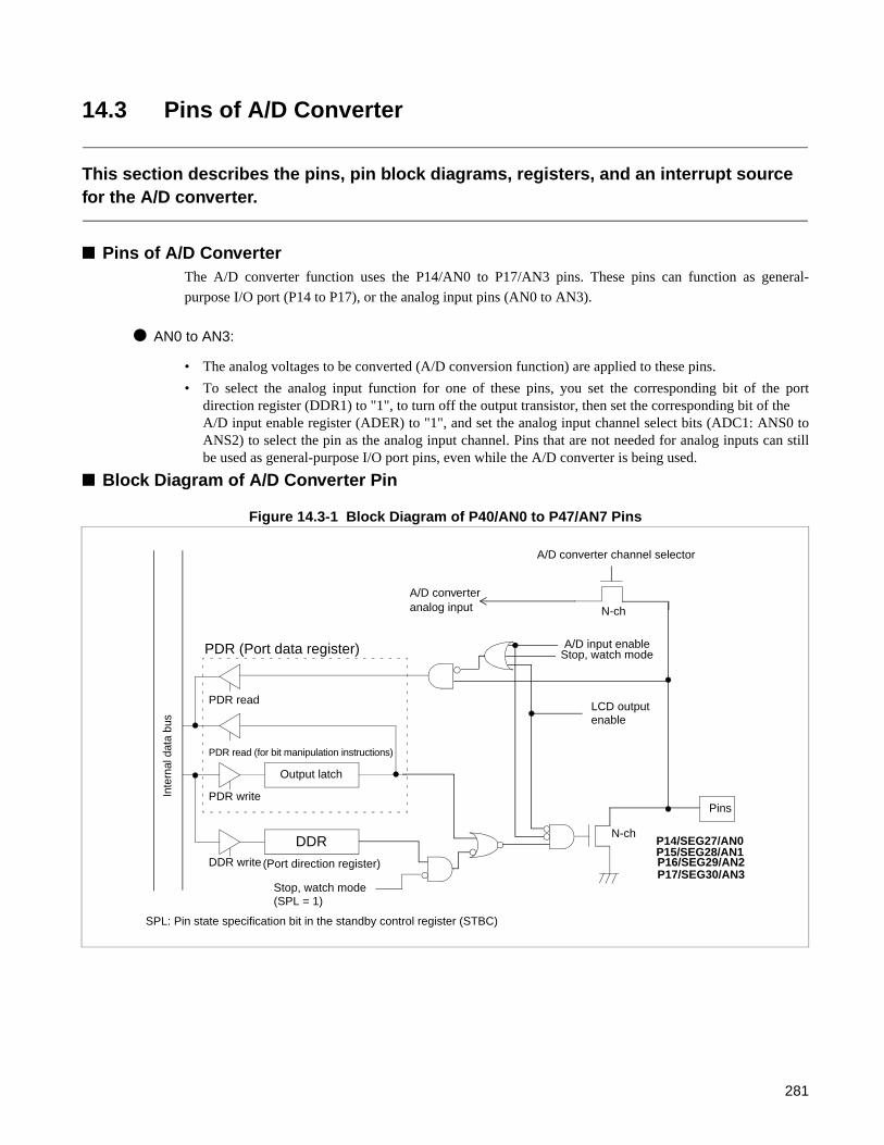
14.3 Pins of A/D Converter
This section describes the pins, pin block diagrams, registers, and an interrupt source for the A/D converter.
Pins of A/D Converter The A/D converter function uses the P14/AN0 to P17/AN3 pins. These pins can function as general-
purpose I/O port (P14 to P17), or the analog input pins (AN0 to AN3).
AN0 to AN3:
• The analog voltages to be converted (A/D conversion function) are applied to these pins.
• To select the analog input function for one of these pins, you set the corresponding bit of the portdirection register (DDR1) to "1", to turn off the output transistor, then set the corresponding bit of the A/D input enable register (ADER) to "1", and set the analog input channel select bits (ADC1: ANS0 toANS2) to select the pin as the analog input channel. Pins that are not needed for analog inputs can stillbe used as general-purpose I/O port pins, even while the A/D converter is being used.
Block Diagram of A/D Converter Pin
Figure 14.3-1 Block Diagram of P40/AN0 to P47/AN7 Pins
PDR (Port data register)
DDR
Inte
rnal
dat
a bu
s
PDR read
PDR read (for bit manipulation instructions)
PDR write
DDR write
Pins
SPL: Pin state specification bit in the standby control register (STBC)
N-ch
Stop, watch mode
Output latch
Stop, watch mode A/D input enable
A/D converteranalog input
A/D converter channel selector
(Port direction register)
P15/SEG28/AN1P14/SEG27/AN0
P16/SEG29/AN2P17/SEG30/AN3
(SPL = 1)
LCD outputenable
N-ch
281

CHAPTER 14 A/D CONVERTER
14.4 Registers of A/D Converter
This section describes the registers of the A/D converter.
Figure 14.4-1 Registers of A/D Converter
A/D Converter Interrupt SourceIRQ8:
The A/D converter generates an interrupt request if an interrupt request output is enabled (ADC2: ADIE =
1) when A/D conversion completes.
ADC1 (A/D control register 1)
ADC2 (A/D control register 2)
ADDH (A/D data register H)
ADDL (A/D data register L)
Address bit7 bit6 bit5 bit4 bit3 bit2 bit1 bit0 Initial value
002CH — ANS2 ANS1 ANS0 ADI ADMV RESV AD -0000000B
R/W R/W R/W R/W R R/W R/W
Address bit7 bit6 bit5 bit4 bit3 bit2 bit1 bit0 Initial value
002DH — RESV RESV ADCK ADIE ADMD EXT RESV -0000001B
R/W R/W R/W R/W R/W R/W R/W
Address bit7 bit6 bit5 bit4 bit3 bit2 bit1 bit0 Initial value
002EH — — — — — — D9 D8 ------XXB
R R
Address bit7 bit6 bit5 bit4 bit3 bit2 bit1 bit0 Initial value
002FH D7 D6 D5 D4 D3 D2 D1 D0 XXXXXXXXB
R R R R R R R R
R/W : Readable/WritableR : Read only— : UndefinedX : Undefined value
282
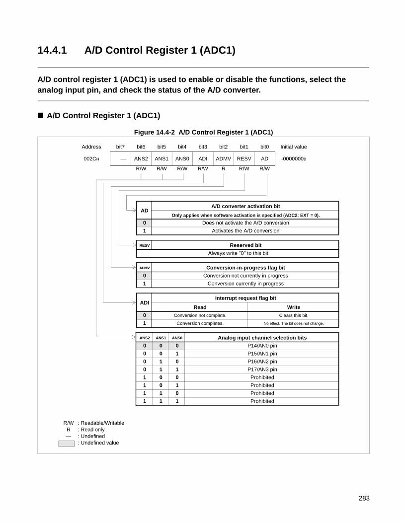
14.4.1 A/D Control Register 1 (ADC1)
A/D control register 1 (ADC1) is used to enable or disable the functions, select the analog input pin, and check the status of the A/D converter.
A/D Control Register 1 (ADC1)
Figure 14.4-2 A/D Control Register 1 (ADC1)
Address bit7 bit6 bit5 bit4 bit3 bit2 bit1 bit0 Initial value
002CH ANS2 ANS1 ANS0 ADI ADMV RESV AD -0000000B
R/W R/W R/W R/W R R/W R/W
ADA/D converter activation bit
Only applies when software activation is specified (ADC2: EXT = 0).
0 Does not activate the A/D conversion
1 Activates the A/D conversion
RESV Reserved bit
Always write "0" to this bit
ADMV Conversion-in-progress flag bit
0 Conversion not currently in progress
1 Conversion currently in progress
ADIInterrupt request flag bit
Read Write
0 Conversion not complete. Clears this bit.
1 Conversion completes. No effect. The bit does not change.
ANS2 ANS1 ANS0 Analog input channel selection bits
0 0 0 P14/AN0 pin
0 0 1 P15/AN1 pin
0 1 0 P16/AN2 pin
0 1 1 P17/AN3 pin
1 0 0 Prohibited
1 0 1 Prohibited
1 1 0 Prohibited
1 1 1 Prohibited
R/W : Readable/WritableR : Read only— : Undefined
: Undefined value
283
CHAPTER 14 A/D CONVERTER
Table 14.4-1 Functions of Bits in A/D Control Register 1 (ADC1)
Bit name Function
bit7 Undefined bit• The read value is undefined. • Writing to this bit has no effect on the operation.
bit6to
bit4
ANS2, AN1, ANS0: Analog input channel selection bits
• These bits select which of the AN0 to AN3 pins to use as the analog input pin.• When using software activation (ADC2: EXT = 0), these bits can be modified at the same
time as activating the A/D conversion (AD = 1). Notes:
• Disable general-purpose port output corresponding to the analog input pin, and set it asanalog input pin by ADER. Do not modify these bits when the ADMV bit is set to "1".
• Pins not used as analog inputs can be used as general-purpose ports.
bit3ADI: Interrupt request flag bit
• This bit is set to "1" when the A/D conversion is completed. • An interrupt request is output when both this bit and the interrupt request enable bit
(ADC2: ADIE) are "1". • Writing "0" clears this bit. Writing "1" has no effect and does not change the bit value.
bit2ADMV: Conversion-in-progress flag bit
• This bit indicates whether or not the A/D converter is currently performing a conversion.• The bit is set to "1" when a conversion is in progress. Note:
This bit is read-only. The write value has no meaning and has no effect on the operation.
bit1RESV:Reserved bit
Note:Always write "0" to this bit.
bit0AD: A/D converter activation bit
• This bit activates the A/D conversion by software. • Writing "1" to this bit activates the A/D conversion when continuous activation is not
specified (ADC2: EXT = 0). Notes:
• Writing "0" to this bit does not stop the A/D conversion. The read value is always "0". • This bit has no meaning when continuous activation is specified.
284
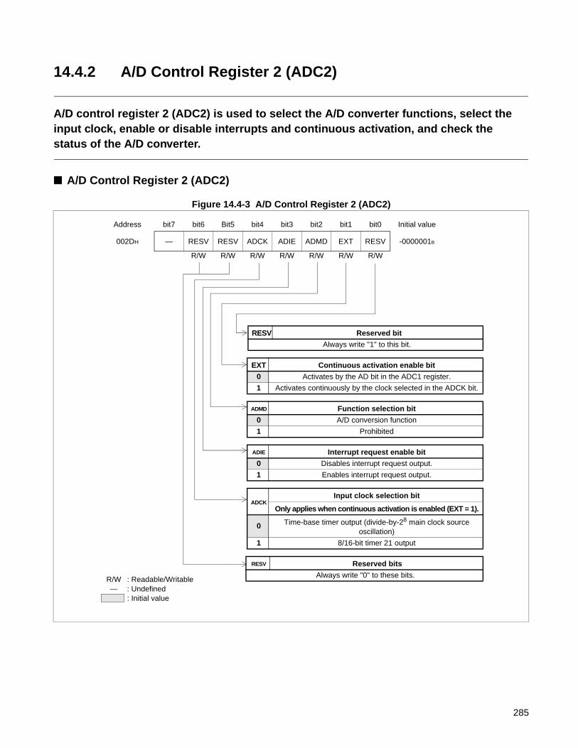
14.4.2 A/D Control Register 2 (ADC2)
A/D control register 2 (ADC2) is used to select the A/D converter functions, select the input clock, enable or disable interrupts and continuous activation, and check the status of the A/D converter.
A/D Control Register 2 (ADC2)
Figure 14.4-3 A/D Control Register 2 (ADC2)
Address bit7 bit6 Bit5 bit4 bit3 bit2 bit1 bit0 Initial value
002DH — RESV RESV ADCK ADIE ADMD EXT RESV -0000001B
R/W R/W R/W R/W R/W R/W R/W
RESV Reserved bit
Always write "1" to this bit.
EXT Continuous activation enable bit
0 Activates by the AD bit in the ADC1 register.
1 Activates continuously by the clock selected in the ADCK bit.
ADMD Function selection bit
0 A/D conversion function
1 Prohibited
ADIE Interrupt request enable bit
0 Disables interrupt request output.
1 Enables interrupt request output.
ADCKInput clock selection bit
Only applies when continuous activation is enabled (EXT = 1).
0 Time-base timer output (divide-by-28 main clock source oscillation)
1 8/16-bit timer 21 output
RESV Reserved bits
Always write "0" to these bits.R/W : Readable/Writable— : Undefined
: Initial value
285
CHAPTER 14 A/D CONVERTER
Table 14.4-2 Functions of Bits in A/D Control Register 2 (ADC2)
Bit name Function
bit7 Undefined bit• The read value is undefined. • Writing to this bit has no effect on the operation.
bit6,bit5
Reserved bitsNote:
Always write "0" to these bits.
bit4ADCK: Input clock selection bit
This bit selects the input clock used to activate the A/D conversion when continuous activation is specified (EXT = 1). Setting this bit to "0" selects the time-base timer
output (divide-by-28 main clock source oscillation). Setting this bit to "1" selects output of 8/16-bit timer 21.
bit3ADIE: Interrupt request enable bit
• This bit enables or disables an interrupt request output to the CPU. • An interrupt request is output when both this bit and the interrupt request flag bit (ADC1: ADI) are "1".
bit2ADMD: Function selection bit
Note:Always write "0" to this bit.
bit1EXT: Continuous activation enable bit
This bit selects whether to activate the A/D conversion by software or to operate continuously synchronized with an input clock.Setting this bit to "0": enables software activation by the A/D converter activation bit
(ADC1: AD). Setting this bit to "1": enables continuous activation on the rising edge of the clock
selected in the input clock selection bit (ADC2: ADCK).
bit0RESV: Reserved bit
Notes:• Always write "1" to this bit. • The read value is always "1".
286
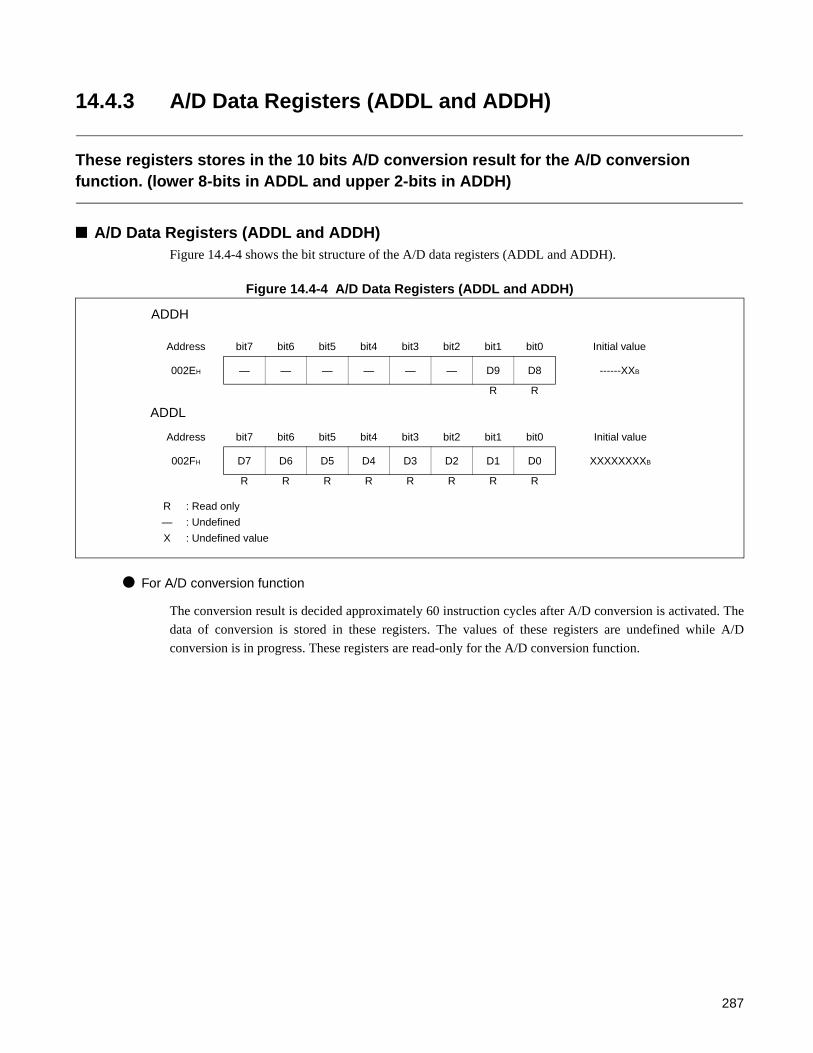
14.4.3 A/D Data Registers (ADDL and ADDH)
These registers stores in the 10 bits A/D conversion result for the A/D conversion function. (lower 8-bits in ADDL and upper 2-bits in ADDH)
A/D Data Registers (ADDL and ADDH)Figure 14.4-4 shows the bit structure of the A/D data registers (ADDL and ADDH).
Figure 14.4-4 A/D Data Registers (ADDL and ADDH)
For A/D conversion function
The conversion result is decided approximately 60 instruction cycles after A/D conversion is activated. The
data of conversion is stored in these registers. The values of these registers are undefined while A/D
conversion is in progress. These registers are read-only for the A/D conversion function.
ADDH
ADDL
R : Read only
— : Undefined
X : Undefined value
Address bit7 bit6 bit5 bit4 bit3 bit2 bit1 bit0 Initial value
002EH — — — — — — D9 D8 ------XXB
R R
Address bit7 bit6 bit5 bit4 bit3 bit2 bit1 bit0 Initial value
002FH D7 D6 D5 D4 D3 D2 D1 D0 XXXXXXXXB
R R R R R R R R
287
CHAPTER 14 A/D CONVERTER
14.5 A/D Converter Interrupt
The A/D converter has the following interrupt:Conversion completion for the A/D conversion function
Interrupt for A/D Conversion Function• When A/D conversion completes, the interrupt request flag bit (ADC1: ADI) is set to "1". At this time,
an interrupt request (IRQ8) to the CPU is generated if the interrupt request enable bit is enabled (ADC2:ADIE = 1). Write "0" to the ADI bit in the interrupt processing routine to clear the interrupt request.
• The ADI bit is set after completion of A/D conversion, regardless of the ADIE bit value.
Note:
An interrupt request is generated immediately if the ADI bit is "1" when the ADIE bit is changed fromdisabled to enabled ("0" -> "1").
Register and Vector Table for A/D Converter Interrupt
Reference:
See "3.4.2 Interrupt Processing" for details on the operation of interrupt.
Table 14.5-1 Register and Vector Table for A/D Converter Interrupt
InterruptInterrupt level settings register Vector table address
Register Setting bits Upper Lower
IRQ8 ILR3 (007DH) L81 (bit1) L80 (bit0) FFEAH FFEBH
288

14.6 Operation of A/D Converter
The A/D conversion functions of the A/D converter can be activated by software or can be activated continuously.
Activating A/D Conversion Function
Software activation
Figure 14.6-1 shows the settings required for software activation of the A/D conversion function.
Figure 14.6-1 A/D Conversion Function (Software Activation) Settings
On activation, the A/D converter starts the operation of the A/D conversion function. The A/D conversion
function can be reactivated while conversion is in progress.
Continuous activation
Figure 14.6-2 shows the settings required for continuous activation of the A/D conversion function.
Figure 14.6-2 A/D Conversion Function (Continuous Activation) Settings
When continuous activation is enabled, the rising edge of the selected input clock activates the A/D
conversion, starting operation of the A/D conversion function. When continuous activation is disabled
(ADC2: EXT = 0), continuous activation halts but software activation is available.
bit7 bit6 bit5 bit4 bit3 bit2 bit1 bit0
ADC1 — ANS2 ANS1 ANS0 ADI ADMV RESV AD
0 1
ADC2 — RESV RESV ADCK ADIE ADMD EXT RESV
0 0 × 0 0 1
ADDL Stores the A/D conversion result.
ADDH Stores the A/D conversion result.
: Used bit× : Unused bit1 : Set "1".0 : Set "0".
bit7 bit6 bit5 bit4 bit3 bit2 bit1 bit0
ADC1 — ANS2 ANS1 ANS0 ADI ADMV RESV AD
0 ×
ADC2 — RESV RESV ADCK ADIE ADMD EXT RESV
0 0 0 1 1
ADDL Stores the A/D conversion value.
ADCH Stores the A/D conversion value.
: Used bit× : Unused bit1 : Set "1".0 : Set "0".
289

CHAPTER 14 A/D CONVERTER
Operation of A/D Conversion Function
The following describes the operation of the A/D converter. The A/D conversion requires approximately 60
instruction cycles from activation to completion.
(1) On activation, A/D conversion sets the conversion-in-progress flag bit (ADC1: ADMV = 1)
and connects the sample hold circuit to the specified analog input pin.
(2) The internal sample hold capacitor captures the voltage at the analog input pin for
approximately 16 instruction cycles. The capacitor holds the voltage until the A/D conversion
completes.
(3) The comparator compares the voltage captured by the sample hold capacitor with the A/D
converter reference voltage starting from the most significant bit (MSB) and ending with the
least significant bit (LSB), and transfers each bit sequentially to the ADDL and ADDH register.
(4) When the complete result has been transferred to the ADDL and ADDH register, the conversion-in-
progress flag bit is cleared (ADC1: ADMV = 0) and the interrupt request flag bit is set
(ADC1: ADI = 1).
290

14.7 Notes on Using A/D Converter
This section lists points to note when using the A/D converter.
Notes on Using A/D Converter
Input impedance of analog input pins
The A/D converter contains a sample hold circuit as shown in Figure 14.7-1 to fetch analog input voltage
into the sample hold capacitor for 16 instruction cycles after activating A/D conversion. For this reason, if
the output impedance of the external circuit for the analog input is high, analog input voltage might not
stabilize within the analog input sampling period. Therefore, it is recommended to keep the output
impedance of the external circuit low (below 10 kΩ). Note that if the impedance cannot be kept low, it is
recommended to connect an external capacitor of about 0.1µF for the analog input pin.
Figure 14.7-1 Analog Input Equivalent Circuit
Notes on setting by program
• For the A/D conversion function, the ADDL and ADDH registers maintain previous values until the
next A/D conversion is activated. However, the content of the ADDL and ADDH registers becomes
indeterminate immediately after activating A/D conversion.
• Do not re-select the analog input channel (ADC1: ANS2 to ANS0) while the A/D conversion is
operating. Particularly, when continuous activation is enabled, only perform such operations after
disabling continuous activation (ADC2: EXT = 0) and waiting for the conversion-in-progress flag bit
(ADC1: ADMV) to go to "0".
• A reset or activation of stop mode stops the A/D converter and initializes all registers.
• Interrupt processing cannot return if the interrupt request flag bit (ADC1: ADI) is "1" and the interrupt
request enable bit is enabled (ADC2: ADIE = 1). Always clear the ADI bit.
Note on interrupt requests
The interrupt request flag bit (ADC1: ADI) is not set if A/D conversion is reactivated (ADC1: AD = 1) at
the same time as the previous A/D conversion completes.
Analog input pin
Sample hold circuit
Comparator
R C
Analog channel selector
Close for 16 instruction cycles afteractivating A/D conversion.
If the analog input impedance is higher than 10 kΩ, it is recommended to connect an external capacitor of approx. 0.1 µF.
291

CHAPTER 14 A/D CONVERTER
Turn-on sequence for A/D converter power supply and analog inputs
• Always apply the A/D converter power supply (AVCC, AVSS) and analog inputs (AN0 to AN3) at thesame time or after turning on the digital power supply (VCC).
• Similarly, when power supply is turned off, always turn off the A/D converter power supply (AVCC,AVSS) and analog inputs (AN0 to AN3) at the same time or before turning off the digital power supply(VCC).
• Take care that AVCC, AVSS, and the analog inputs do not exceed the digital power supply voltage whenturning the A/D converter power supply on or off.
Conversion time
A/D conversion function conversion time is affected by oscillator frequency, and main clock speed
switching (speed shift function).
Continuous activation input clock
The time-base timer output, which can be selected as input clock, is not affected by the speed shift function.
Note also that the cycle time is affected (for one cycle) when the time-base timer is cleared.
292
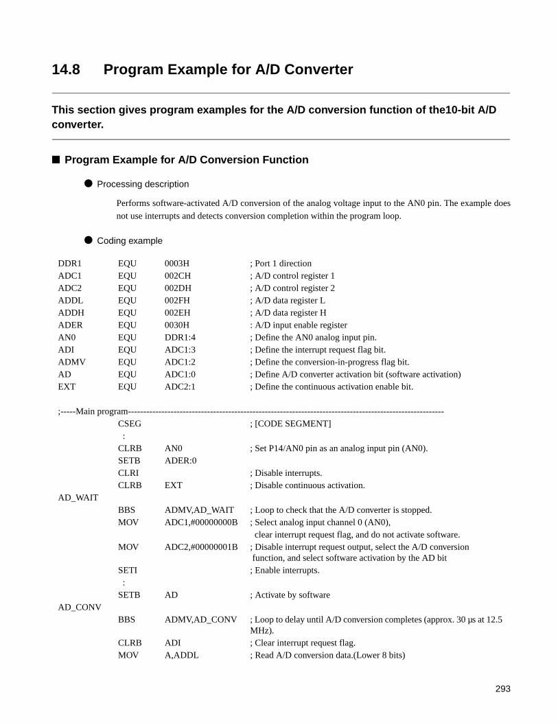
14.8 Program Example for A/D Converter
This section gives program examples for the A/D conversion function of the10-bit A/D converter.
Program Example for A/D Conversion Function
Processing description
Performs software-activated A/D conversion of the analog voltage input to the AN0 pin. The example does
not use interrupts and detects conversion completion within the program loop.
Coding example
DDR1 EQU 0003H ; Port 1 directionADC1 EQU 002CH ; A/D control register 1ADC2 EQU 002DH ; A/D control register 2ADDL EQU 002FH ; A/D data register LADDH EQU 002EH ; A/D data register HADER EQU 0030H : A/D input enable registerAN0 EQU DDR1:4 ; Define the AN0 analog input pin.ADI EQU ADC1:3 ; Define the interrupt request flag bit.ADMV EQU ADC1:2 ; Define the conversion-in-progress flag bit.AD EQU ADC1:0 ; Define A/D converter activation bit (software activation)EXT EQU ADC2:1 ; Define the continuous activation enable bit.
;-----Main program--------------------------------------------------------------------------------------------------------CSEG ; [CODE SEGMENT]:
CLRB AN0 ; Set P14/AN0 pin as an analog input pin (AN0).SETB ADER:0CLRI ; Disable interrupts.CLRB EXT ; Disable continuous activation.
AD_WAITBBS ADMV,AD_WAIT ; Loop to check that the A/D converter is stopped.MOV ADC1,#00000000B ; Select analog input channel 0 (AN0),
clear interrupt request flag, and do not activate software.MOV ADC2,#00000001B ; Disable interrupt request output, select the A/D conversion
function, and select software activation by the AD bitSETI ; Enable interrupts.:
SETB AD ; Activate by softwareAD_CONV
BBS ADMV,AD_CONV ; Loop to delay until A/D conversion completes (approx. 30 µs at 12.5 MHz).
CLRB ADI ; Clear interrupt request flag.MOV A,ADDL ; Read A/D conversion data.(Lower 8 bits)
293

CHAPTER 14 A/D CONVERTER
MOV A,ADDH ; Read A/D conversion data (upper 2 bits)::
ENDS;-------------------------------------------------------------------------------------------------------------------------------
END
294

CHAPTER 15UART/SIO
This chapter describes the functions and operation of the UART/SIO.
15.1 Overview of UART/SIO
15.2 Block Diagram of UART/SIO
15.3 Pins of UART/SIO
15.4 Registers of UART/SIO
15.5 UART/SIO Interrupts
15.6 Operation of UART/SIO
15.7 Operation of mode 0
15.8 Operation of mode 1
295

CHAPTER 15 UART/SIO
15.1 Overview of UART/SIO
The UART/SIO is a general-purpose serial data communication interface. The UART/SIO supports both synchronous and asynchronous mode operation and transmits variable-length serial data. The transfer format is the "NRZ" system and the transfer data rate is configured by setting the dedicated baud rate generator, external clocks, or internal timers.
Function of UART/SIO The UART/SIO communicates with other CPUs and peripheral devices by sending/receiving serial data
(serial input/output).
• The full-duplex double buffer embedded in the device enables full-duplex bi-directional
communication.
• Users can configure the UART/SIO to the synchronous transfer mode or asynchronous transfer mode.
• Internal baud rate generator allows users to select a baud rate from 14 different speeds. The baud rate is
also configured by setting external clock inputs.
• The variable data length system allows users to set the data length at 7 to 8-bit non-parity or 8 to 9-bit
parity mode (See Table 15.1-1).
• The data transfer format is based on the NRZ (Non Return to Zero) system.
Table 15.1-1 UART/SIO Operating Mode
Operating ModeData Length
Transfer Mode Stop Bit LengthNon-parity Parity
07 bits 8 bits
Asynchronous 1 bit or 2 bits8 bits 9 bits
1 8 bits Synchronous —
296
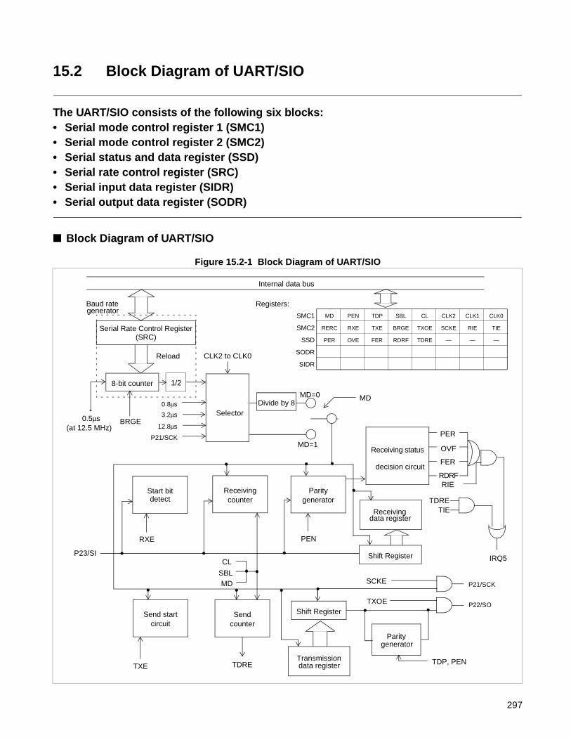
15.2 Block Diagram of UART/SIO
The UART/SIO consists of the following six blocks:• Serial mode control register 1 (SMC1)• Serial mode control register 2 (SMC2)• Serial status and data register (SSD)• Serial rate control register (SRC)• Serial input data register (SIDR)• Serial output data register (SODR)
Block Diagram of UART/SIO
Figure 15.2-1 Block Diagram of UART/SIO
OVF
FER
RDRF
Internal data bus
Serial Rate Control Register
8-bit counter
Reload
0.5µs(at 12.5 MHz)
Baud rategenerator
0.8µs
3.2µs
12.8µs
P21/SCK
SelectorDivide by 8
BRGE
MD
Start bitdetect
Receiving Parity
Send start Send
Transmission
Shift Register
Parity
Receiving
Receiving status
P23/SI
RXE PEN
CL
SBLMD
TXOE
SCKE
counter generator
decision circuit
circuit counter
data register
generator
RIE
TDRETIE
IRQ5
TXE TDRE TDP, PEN
CLK2 to CLK0
P21/SCK
P22/SO
MD=1
MD=0
PER
data register
Shift Register
Registers:
SMC1 MD PEN TDP SBL CL CLK2 CLK1 CLK0
SMC2 RERC RXE TXE BRGE TXOE SCKE RIE TIE
SSD PER OVE FER RDRF TDRE — — —
SODR
SIDR
(SRC)
1/2
297
CHAPTER 15 UART/SIO
Serial Mode Control Registers (SMC1 and SMC2)
These registers control operating modes in the UART/SIO. The register sets transfer mode (synchronous/
asynchronous), parity/non-parity, stop bit length, operating mode (data length), transmission data rate,
enable/disable of UART/SIO operation, enable/disable of serial clock output, enable/disable of serial output
and enable/disable of interrupt request to CPU.
Serial Rate Control Register (SRC)
This register controls the data transmission rate (baud rate). The register selects transfer rate generated by
baud rate generator.
Serial Status and Data Register (SSD)
This register shows UART/SIO sending/receiving, error status, as well as receives parity.
Serial Input Data Register (SIDR)
This register holds received data. Serial data received is converted and stored in the register. When the data
length is set to 7 bits, bit7 does not have meaning.
Serial Output Data Register (SODR)
This register sets sending data. The data written in this register is converted to the serial data and output.
When the data length is set to 7 bits, bit7 does not have meaning.
298
15.3 Pins of UART/SIO
This section describes the pins and pin block diagram of UART/SIO.
Pin of UART/SIOThe pins for the UART/SIO function are shift clock input/output pin (P21/SCK), serial data output pin
(P22/SO) and serial data input pin (P23/SI).
P21/SCK :
• This pin function either as a general purpose input/output port (P21) or a clock input/output pin(hysteresis input) for the UART/SIO(SCK).
When clock output is enabled (SMC2: SCKE=1), this pin function as clock output pin (SCK)
irrespective of settings on corresponding port direction register. In this case, do not select an external
clock (SMC1: CLK2, CLK1, CLK0 do not select 100B).
• To use the port as a UART/SIO clock input pin, disable the clock output (SMC2: SCKE = 0) andconfigure the port as an input port by setting a corresponding port direction register bit (DDR2: bit1 =0). In this case, be sure to select an external clock (SMC1: CLK2, CLK1, CLK0 = 100B).
P22/SO :
This pin function either as general-purpose input/output port (P22) or serial data output pin of the
UART/SIO (SO).
When serial data output is enabled (SMC2: TXOE=1), this pin function as serial data output pin of the
UART/SIO irrespective of settings on corresponding port direction register.
P23/SI :
This pin function either as general-purpose input/output port (P23) or serial data input pin (hysteresis
input) of the UART/SIO (SI).
To use the port as a UART/SIO serial data input pin, configure the port as input port by setting a
corresponding bit of the port direction register (DDR2: bit3 = 0).
299

CHAPTER 15 UART/SIO
Block Diagram of UART/SIO Pin
Figure 15.3-1 Block Diagram of UART/SIO Pin
Note:
When pull-up resistor is selected in pull-up resistor control register, the states of these pins in stopand watch mode (SPL=1) are in "H" level (pull-up state) rather than high impedance. However,during reset, pull-up is unavailable and will be in high impedance state.
PDR (Port data register)
DDR
Inte
rnal
dat
a bu
s
PDR read
PDR read (for bit manipulation instructions)
Output latch
PDR write
DDR write
Pins
SPL: Pin state specification bit in the standby control register (STBC)
N-ch
Stop, watch mode
To UART/SIO SCK, SI
(Port data
UART/SIO output
Stop, watch mode
P-ch
direction register)
DDR read
Pull-up resistor
P-ch
Pull-up resistor control register
Output enable
Approx. 50kΩ
P21/SCKP22/SOP23/SI
(SPL = 1)
300

15.4 Registers of UART/SIO
This section describes the registers of the UART/SIO.
Registers of UART/SIO
Figure 15.4-1 Registers of UART/SIO
SMC1 (Serial mode control register 1)
SMC2 (Serial mode control register 2)
SRC (Serial rate control register)
SSD (Serial status and data register)
SIDR (Serial input data register)
SODR (Serial output data register)
Address bit7 bit6 bit5 bit4 bit3 bit2 bit1 bit0 Initial value
0020H MD PEN TDP SBL CL CLK2 CLK1 CLK0 00000000B
R/W R/W R/W R/W R/W R/W R/W R/W
Address bit7 bit6 bit5 bit4 bit3 bit2 bit1 bit0 Initial value
0021H RERC RXE TXE BRGE TXOE SCKE RIE TIE 00000000B
W R/W R/W W R/W R/W R/W R/W
Address bit7 bit6 bit5 bit4 bit3 bit2 bit1 bit0 Initial value
0022H XXXXXXXXB
R/W R/W R/W R/W R/W R/W R/W R/W
Address bit7 bit6 bit5 bit4 bit3 bit2 bit1 bit0 Initial value
0023H PER OVE FER RDRF TDRE — — — 00001---B
R R R R R
Address bit7 bit6 bit5 bit4 bit3 bit2 bit1 bit0 Initial value
0024H XXXXXXXXB
R R R R R R R R
Address bit7 bit6 bit5 bit4 bit3 bit2 bit1 bit0 Initial value
0024H XXXXXXXXB
W W W W W W W W
R/W : Readable/WritableR : Read onlyW : Write only— : UndefinedX : Undefined value
301

CHAPTER 15 UART/SIO
15.4.1 Serial Mode Control Register 1 (SMC1)
Serial mode control register 1 (SMC1) sets transfer mode (synchronous/asynchronous), stop bit length, data length, parity/non-parity and selects the serial clock.
Serial Mode Control Register 1 (SMC1)
Figure 15.4-2 Serial Mode Control Register 1 (SMC1)
Address bit7 bit6 bit5 bit4 bit3 bit2 bit1 bit0 Initial value
0020H MD PEN TDP SBL CL CLK2 CLK1 CLK0 00000000B
R/W R/W R/W R/W R/W R/W R/W R/W
CLK2 CLK1 CLK0 Clock selection bits0 0 0 2 instruction cycles0 0 1 8 instruction cycles0 1 0 32 instruction cycles0 1 1 Dedicated baud rate generator1 0 0 External clock
CL Character bit length control bit0 7-bit data length1 8-bit data length
SBL Stop bit length control bit0 1-bit length1 2-bit length
TDP Parity polarity bit0 Even parity1 Odd parity
PEN Parity control bit0 Non-parity1 Parity (odd/even selected by TDP bit)
MD Mode control bit0 Asynchronous mode (UART)1 Synchronous mode (SIO)
R/W : Readable/Writable: Initial value
302

Table 15.4-1 Functions of Bits in Serial Mode Control Register 1 (SMC1)
Bit name Function
bit7MD:Mode control bit
This bit selects the UART/SIO operating mode. In asynchronous mode, the UART/SIO operates on the serial clock divided by 8. In synchronous mode, it operates on the selected serial clock.
bit6PEN:Parity control bit
In asynchronous mode operation, this bit sets whether there is parity data or not.
bit5TDP:Parity polarity bit
In asynchronous mode operation, this bit decides which sort of parity data during serial transmission. During serial receiving, it checks parity data.
bit4SBL:Stop bit length control bit
This bit determines the stop bit length in clock asynchronous mode operation.• In serial transmissions, a stop bit of the bit length specified is appended.• In serial receiving, a stop bit is recognized as in a 1-bit length regardless of the value
set here.
bit3CL:Character bit length control bit
This bit sets the character bit length in asynchronous mode operation.
bit2to
bit0
CLK2, CLK1, CLK0:Clock selection bits
These bits select the serial clock.
303

CHAPTER 15 UART/SIO
15.4.2 Serial Mode Control Register 2 (SMC2)
Serial mode control register 2 (SMC2) sets the serial data output enable to pins, clock output enable to pins, transmission/receiving interrupt enable and baud rate generator start bit.
Serial Mode Control Register 2 (SMC2)
Figure 15.4-3 Serial Mode Control Register 2 (SMC2)
Address bit7 bit6 bit5 bit4 bit3 bit2 bit1 bit0 Initial value
0021H RERC RXE TXE BRGE TXOE SCKE RIE TIE 00000000B
W R/W R/W W R/W R/W R/W R/W
TIE Transmission interrupt enable bit0 Disable transmission interrupt1 Enable transmission interrupt
RIE Receiving interrupt enable bit0 Disable receiving interrupt1 Enable receiving interrupt
SCKE Serial Clock output enable bit
0 P21/SCK functions as a general purpose I/O port or shift clock input
1 P21/SCK functions as shift clock output
TXOE Serial data output enable bit0 P22/SO functions as a general purpose I/O port1 P22/SO functions as serial data output
BRGE Baud rate generator start bit0 Stops the baud rate generator1 Starts the baud rate generator
TXE Transmission operation enable bit0 Disables transmission operations1 Enables transmission operations
RXE Receiving operation enable bit0 Disables receiving operations1 Enables receiving operations
RERC Receiving every flag clear bit0 Clears all error flags1 No change to this bit, no effect on the other bitsR/W : Readable/Writable
W : Write only: Initial value
304
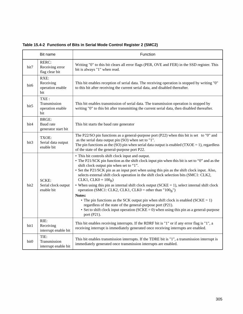
Table 15.4-2 Functions of Bits in Serial Mode Control Register 2 (SMC2)
Bit name Function
bit7RERC:Receiving error flag clear bit
Writing "0" to this bit clears all error flags (PER, OVE and FER) in the SSD register. This bit is always "1" when read.
bit6
RXE:Receiving operation enable bit
This bit enables reception of serial data. The receiving operation is stopped by writing "0" to this bit after receiving the current serial data, and disabled thereafter.
bit5
TXE :Transmission operation enable bit
This bit enables transmission of serial data. The transmission operation is stopped by writing "0" to this bit after transmitting the current serial data, then disabled thereafter.
bit4BRGE:Baud rate generator start bit
This bit starts the baud rate generator
bit3TXOE:Serial data output enable bit
The P22/SO pin functions as a general-purpose port (P22) when this bit is set to "0" and as the serial data output pin (SO) when set to "1".The pin functions as the (SO) pin when serial data output is enabled (TXOE = 1), regardless of the state of the general-purpose port P22.
bit2SCKE:Serial clock output enable bit
• This bit controls shift clock input and output.• The P21/SCK pin function as the shift clock input pin when this bit is set to “0” and as the
shift clock output pin when set to “1”.• Set the P21/SCK pin as an input port when using this pin as the shift clock input. Also,
selects external shift clock operation in the shift clock selection bits (SMC1: CLK2, CLK1, CLK0 = 100B)
• When using this pin as internal shift clock output (SCKE = 1), select internal shift clock operation (SMC1: CLK2, CLK1, CLK0 = other than "100B")
Notes:• The pin functions as the SCK output pin when shift clock is enabled (SCKE = 1)
regardless of the state of the general-purpose port (P21).• Set to shift clock input operation (SCKE = 0) when using this pin as a general-purpose
port (P21).
bit1RIE:Receiving interrupt enable bit
This bit enables receiving interrupts. If the RDRF bit is "1" or if any error flag is "1", a receiving interrupt is immediately generated once receiving interrupts are enabled.
bit0TIE:Transmission interrupt enable bit
This bit enables transmission interrupts. If the TDRE bit is "1", a transmission interrupt is immediately generated once transmission interrupts are enabled.
305

CHAPTER 15 UART/SIO
15.4.3 Serial Status and Data Register (SSD)
The serial status and data register (SSD) is used to set and monitor transmit/receive operations, error status.
Serial Status and Data Register (SSD)
Figure 15.4-4 Serial Status and Data Register (SSD)
Address bit7 bit6 bit5 bit4 bit3 bit2 bit1 bit0 Initial value
0023H PER OVE FER RDRF TDRE — — — 00001---B
R R R R R
TDRE Transmission data register empty0 Full of transmission data1 Empty
RDRF Receive data register full0 Empty1 Full of receiving data
FER Framing error flag0 No frame error1 Framing error
OVE Overrun error flag0 No overrun error1 Overrun error
PER Parity error flag0 No parity error1 Parity error
R : Read only— : Undefined
: Initial value
306
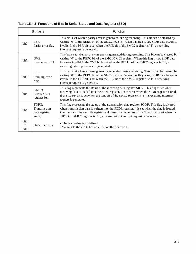
Table 15.4-3 Functions of Bits in Serial Status and Data Register (SSD)
Bit name Function
bit7PER:Parity error flag
This bit is set when a parity error is generated during receiving. This bit can be cleared by writing "0" to the RERC bit of the SMC2 register. When this flag is set, SIDR data becomes invalid. If the PER bit is set when the RIE bit of the SMC2 register is "1", a receiving interrupt request is generated.
bit6OVE:overrun error bit
This bit is set when an overrun error is generated during receiving. This bit can be cleared by writing "0" to the RERC bit of the SMC1/SMC2 register. When this flag is set, SIDR data becomes invalid. If the OVE bit is set when the RIE bit of the SMC2 register is "1", a receiving interrupt request is generated.
bit5FER:Framing error flag
This bit is set when a framing error is generated during receiving. This bit can be cleared by writing "0" to the RERC bit of the SMC2 register. When this flag is set, SIDR data becomes invalid. If the FER bit is set when the RIE bit of the SMC2 register is "1", a receiving interrupt request is generated.
bit4RDRF:Receive data register full
This flag represents the status of the receiving data register SIDR. This flag is set when receiving data is loaded into the SIDR register. It is cleared when the SIDR register is read. If the RDRF bit is set when the RIE bit of the SMC2 register is "1", a receiving interrupt request is generated.
bit3
TDRE:Transmission data register empty
This flag represents the status of the transmission data register SODR. This flag is cleared when transmission data is written into the SODR register. It is set when the data is loaded into the transmission shift register and transmission begins. If the TDRE bit is set when the TIE bit of SMC2 register is "1", a transmission interrupt request is generated.
bit2to
bit0Undefined bits
• The read value is undefined. • Writing to these bits has no effect on the operation.
307
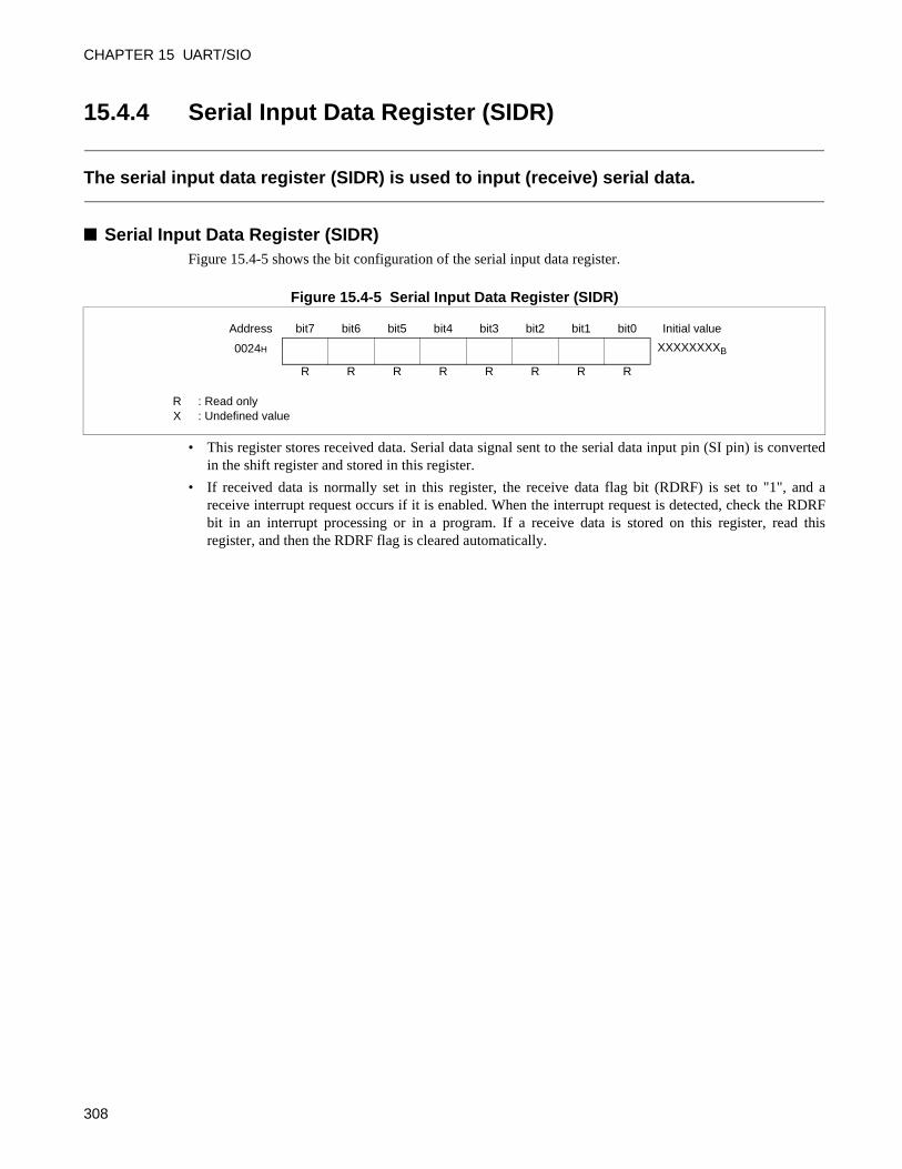
CHAPTER 15 UART/SIO
15.4.4 Serial Input Data Register (SIDR)
The serial input data register (SIDR) is used to input (receive) serial data.
Serial Input Data Register (SIDR)Figure 15.4-5 shows the bit configuration of the serial input data register.
Figure 15.4-5 Serial Input Data Register (SIDR)
• This register stores received data. Serial data signal sent to the serial data input pin (SI pin) is convertedin the shift register and stored in this register.
• If received data is normally set in this register, the receive data flag bit (RDRF) is set to "1", and areceive interrupt request occurs if it is enabled. When the interrupt request is detected, check the RDRFbit in an interrupt processing or in a program. If a receive data is stored on this register, read thisregister, and then the RDRF flag is cleared automatically.
Address bit7 bit6 bit5 bit4 bit3 bit2 bit1 bit0 Initial value
0024H XXXXXXXXB
R R R R R R R R
R : Read onlyX : Undefined value
308
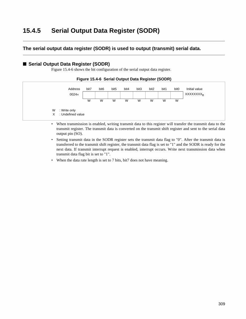
15.4.5 Serial Output Data Register (SODR)
The serial output data register (SODR) is used to output (transmit) serial data.
Serial Output Data Register (SODR)Figure 15.4-6 shows the bit configuration of the serial output data register.
Figure 15.4-6 Serial Output Data Register (SODR)
• When transmission is enabled, writing transmit data to this register will transfer the transmit data to thetransmit register. The transmit data is converted on the transmit shift register and sent to the serial dataoutput pin (SO).
• Setting transmit data in the SODR register sets the transmit data flag to "0". After the transmit data istransferred to the transmit shift register, the transmit data flag is set to "1" and the SODR is ready for thenext data. If transmit interrupt request is enabled, interrupt occurs. Write next transmission data whentransmit data flag bit is set to "1".
• When the data rate length is set to 7 bits, bit7 does not have meaning.
Address bit7 bit6 bit5 bit4 bit3 bit2 bit1 bit0 Initial value
0024H XXXXXXXXB
W W W W W W W W
W : Write onlyX : Undefined value
309

CHAPTER 15 UART/SIO
15.4.6 Serial Rate Control Register (SRC)
The serial rate control register (SRC) is to set the UART/SIO transmission speed (baud rate).
Serial rate control register (SRC)Figure 15.4-7 shows the bit configuration of the serial rate control register.
Figure 15.4-7 Serial rate control register (SRC)
When the clock selection bits, CLK2 to CLK0 of SMC1, are set to "011B", the dedicated baud rate
generator is selected as the serial clock. Also, be sure to write to this register only when the UART/SIO
operations are stopped.
Address bit7 bit6 bit5 bit4 bit3 bit2 bit1 bit0 Initial value
0022H XXXXXXXXB
R/W R/W R/W R/W R/W R/W R/W R/W
R/W : Readable/WritableX : Undefined value
310
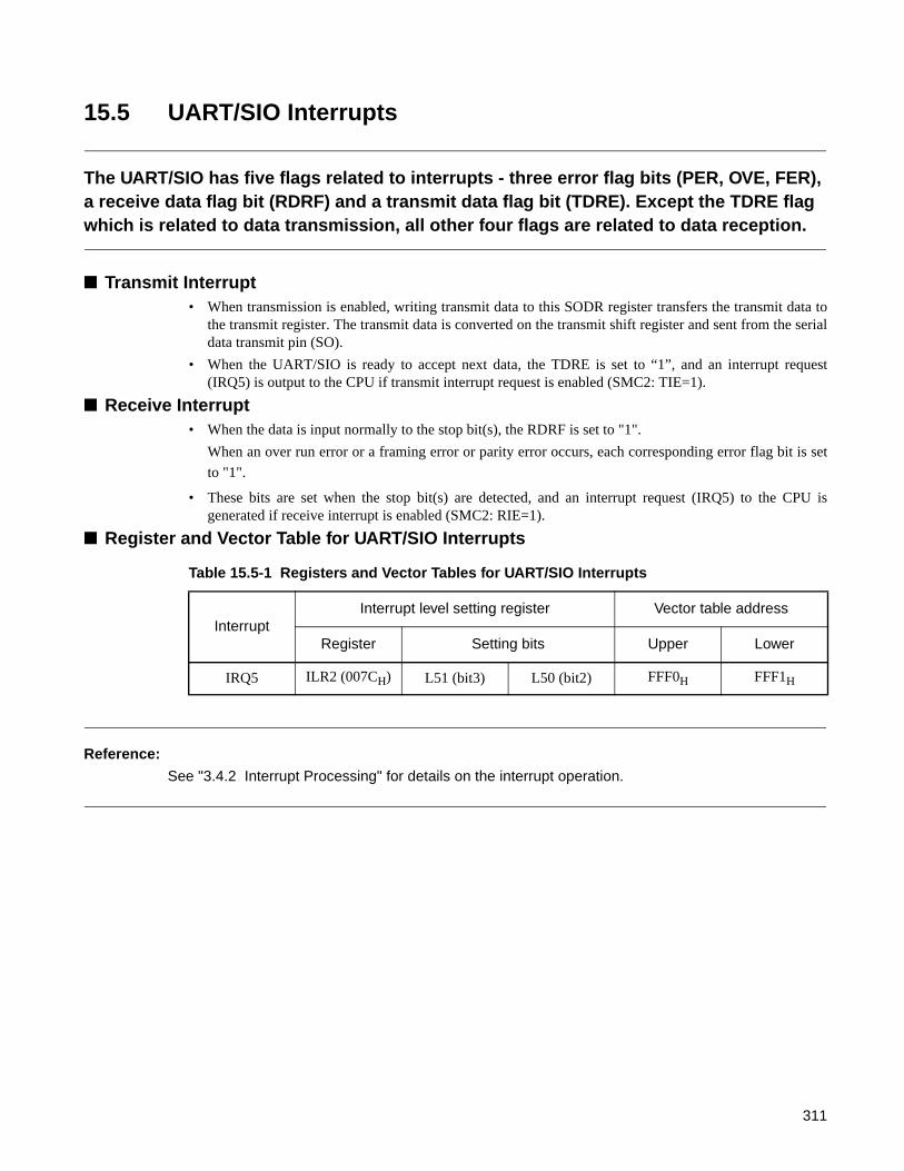
15.5 UART/SIO Interrupts
The UART/SIO has five flags related to interrupts - three error flag bits (PER, OVE, FER), a receive data flag bit (RDRF) and a transmit data flag bit (TDRE). Except the TDRE flag which is related to data transmission, all other four flags are related to data reception.
Transmit Interrupt• When transmission is enabled, writing transmit data to this SODR register transfers the transmit data to
the transmit register. The transmit data is converted on the transmit shift register and sent from the serialdata transmit pin (SO).
• When the UART/SIO is ready to accept next data, the TDRE is set to “1”, and an interrupt request(IRQ5) is output to the CPU if transmit interrupt request is enabled (SMC2: TIE=1).
Receive Interrupt• When the data is input normally to the stop bit(s), the RDRF is set to "1".
When an over run error or a framing error or parity error occurs, each corresponding error flag bit is set
to "1".
• These bits are set when the stop bit(s) are detected, and an interrupt request (IRQ5) to the CPU isgenerated if receive interrupt is enabled (SMC2: RIE=1).
Register and Vector Table for UART/SIO Interrupts
Reference:
See "3.4.2 Interrupt Processing" for details on the interrupt operation.
Table 15.5-1 Registers and Vector Tables for UART/SIO Interrupts
InterruptInterrupt level setting register Vector table address
Register Setting bits Upper Lower
IRQ5 ILR2 (007CH) L51 (bit3) L50 (bit2) FFF0H FFF1H
311

CHAPTER 15 UART/SIO
15.6 Operation of UART/SIO
This section describes the operation of the UART/SIO.The UART/SIO has a serial communication function (operation mode 0 and 1).
Operation of UART/SIO
Operation mode
The UART/SIO has 2 operation modes. The modes 0 and 1 are standard serial transmission modes in which
a data type from 7 bit data length/parity or 8 bit data length/non-parity is selected (See Table 15.5-1).
312

15.7 Operation of mode 0
The operating mode 0 provides an asynchronous mode operation.
Operation of Operating Mode 0 • The serial clock is selected by the bits CLK2 to CLK0 of the SMC1 register. Selection can be made
from five sources: three internal clock outputs, one external clock output, and one baud rate generatoroutput. Always be sure to input a clock when the external clock has been selected.
• In clock asynchronous mode, the shift clock selected by the bits CLK2 to CLK0 is divided by eight foruse as the baud rate generator. Data transfer in the range -2% to +2% of the selected baud rate ispossible.
Figure 15.7-1 Transmit Operation in Mode 0 (CLK2, CLK1, CLK0 not equal to 011B)
Figure 15.7-2 Transmit Operation in Mode 0 (CLK2, CLK1, CLK0 = 011B)
Baud rate = 1
8 ×
(bps)
Clock selection from CLK2 to CLK0
Baud rate = 1
8 × 2 × n ×
(bps)
4/FCH8/FCH16/FCH64/FCH
speed-shift selection
FCH : Main clock source oscillation frequency n : Value of serial rate control register SRC
Table 15.7-1 Baud Rate Setting
Frequency FCH 12.5MHz 8MHz 7.3728MHz 4.9152MHz
Instruction cycle 4/FCH(0.32µs) 4/FCH(0.5µs) 4/FCH(0.54µs) 4/FCH(0.81µs)
Baud rate
97656(n=2) 62500(n=2) — 76800(n=1)
48828(n=4) 31250(n=4) 38400(n=3) 38400(n=2)
13020(n=15) 10417(n=12) 19200(n=6) 19200(n=4)
12207 (n=16) 9615 (n=13) 9600 (n=12) 9600 (n=8)
6104 (n=32) 4807 (n=26) 4800 (n=24) 4800 (n=16)
3004 (n=65) 2403 (n=52) 2400 (n=48) 2400 (n=32)
1502 (n=130) 1201 (n=104) 1200 (n=96) 1200 (n=64)
— 600 (n=208) 600 (n=192) 600 (n=128)
— — — 300 (n=0)
313
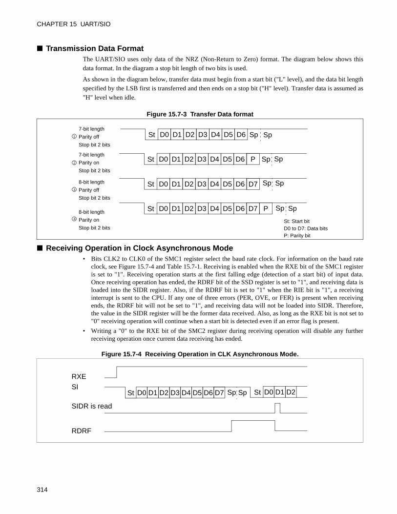
CHAPTER 15 UART/SIO
Transmission Data FormatThe UART/SIO uses only data of the NRZ (Non-Return to Zero) format. The diagram below shows this
data format. In the diagram a stop bit length of two bits is used.
As shown in the diagram below, transfer data must begin from a start bit ("L" level), and the data bit length
specified by the LSB first is transferred and then ends on a stop bit ("H" level). Transfer data is assumed as
"H" level when idle.
Figure 15.7-3 Transfer Data format
Receiving Operation in Clock Asynchronous Mode• Bits CLK2 to CLK0 of the SMC1 register select the baud rate clock. For information on the baud rate
clock, see Figure 15.7-4 and Table 15.7-1. Receiving is enabled when the RXE bit of the SMC1 registeris set to "1". Receiving operation starts at the first falling edge (detection of a start bit) of input data.Once receiving operation has ended, the RDRF bit of the SSD register is set to "1", and receiving data isloaded into the SIDR register. Also, if the RDRF bit is set to "1" when the RIE bit is "1", a receivinginterrupt is sent to the CPU. If any one of three errors (PER, OVE, or FER) is present when receivingends, the RDRF bit will not be set to "1", and receiving data will not be loaded into SIDR. Therefore,the value in the SIDR register will be the former data received. Also, as long as the RXE bit is not set to"0" receiving operation will continue when a start bit is detected even if an error flag is present.
• Writing a "0" to the RXE bit of the SMC2 register during receiving operation will disable any furtherreceiving operation once current data receiving has ended.
Figure 15.7-4 Receiving Operation in CLK Asynchronous Mode.
D0 D1 D2 D3 D4 D5 D6 SpSt
PD0 D1 D2 D3 D4 D5 D6St
D0 D1 D2 D3 D4 D5 D6St
D0 D1 D2 D3 D4 D5 D6St
Sp
Sp Sp
D7 Sp Sp
Sp SpPD7
D0 to D7: Data bitsP: Parity bit
7-bit length
Parity off
Stop bit 2 bits
7-bit length
Parity on
Stop bit 2 bits
8-bit length
Parity off
Stop bit 2 bits
8-bit length
Parity on
Stop bit 2 bitsSt: Start bit
1
2
3
4
D0 D1 D2 D3 D4 D5 D6St Sp SpD7 D0 D1 D2St
RXE
SI
SIDR is read
RDRF
314

Receiving Errors in Asynchronous Mode
• Three types of error detection are performed in asynchronous mode. The three errors are: parity error,overrun error, and framing error. When an error is detected, a "1" is set in the corresponding PER, OVE,or FER bit of the SSD register.
• These errors are detected as described below when receiving ends. When any of these errors is detected,the RDRF bit will not be set, and receiving data will not be loaded into the SIDR register. Therefore thevalue in the SIDR register will be last data received. Also, these error flags can all be cleared by writing"0" into the RERC bit of the SMC2 register.
Figure 15.7-5 Set Timing for receive errors
Detecting the Start Bit during Receiving OperationThe start bit is recognized when a "L" level is present for four clock pulses of the selected serial clock
(clock generator output, and so on.) after the first falling edge of input data. After the start bit is detected,
data is sampled at the rising edge of the fifth clock pulse of the serial clock
Figure 15.7-6 Start Bit Detection
D5
Error interrupt
D6 D7/P Sp SpSI
PEROVEFER
1 2 3 4 5 6 7 8 1 2 3 4 5 6 7 8
Serial clock
4 clock pulses
Start bit detected
D0
Data sampled St: Start bitD0 to D7: Data bits
SI1
315
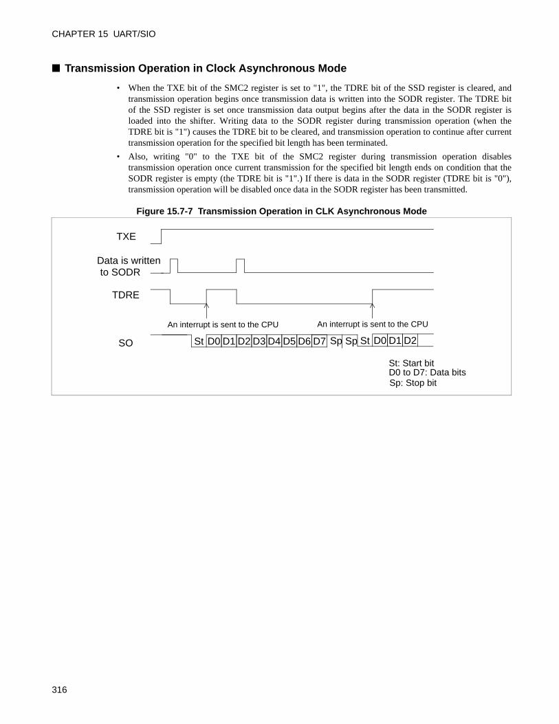
CHAPTER 15 UART/SIO
Transmission Operation in Clock Asynchronous Mode
• When the TXE bit of the SMC2 register is set to "1", the TDRE bit of the SSD register is cleared, andtransmission operation begins once transmission data is written into the SODR register. The TDRE bitof the SSD register is set once transmission data output begins after the data in the SODR register isloaded into the shifter. Writing data to the SODR register during transmission operation (when theTDRE bit is "1") causes the TDRE bit to be cleared, and transmission operation to continue after currenttransmission operation for the specified bit length has been terminated.
• Also, writing "0" to the TXE bit of the SMC2 register during transmission operation disablestransmission operation once current transmission for the specified bit length ends on condition that theSODR register is empty (the TDRE bit is "1".) If there is data in the SODR register (TDRE bit is "0"),transmission operation will be disabled once data in the SODR register has been transmitted.
Figure 15.7-7 Transmission Operation in CLK Asynchronous Mode
D0 D1 D2 D3 D4 D5 D6St Sp SpD7 D0 D1 D2St
TXE
Data is written to SODR
TDRE
SO
An interrupt is sent to the CPU An interrupt is sent to the CPU
St: Start bitD0 to D7: Data bitsSp: Stop bit
316

15.8 Operation of mode 1
The operating mode 1 provides a clock synchronous mode operation.
Operation of Operating Mode 1• In synchronous mode, the CLK2 to CLK0 bits of the SMC1 register select the clock from one of five
source: three internal clocks, an external clock, or the baud rate generator. Shift operation are thenperformed using the selected clock as a shift clock. Be sure to set the SCKE bit of SMC2 to "0" when anexternal clock is input.
• Also, be sure to set the SCKE bit to "1" if outputting an internal clock or baud rate generator as the shiftclock. The following equation is show the calculating the baud rate in synchronous mode
Figure 15.8-1 Transmit Operation in Mode 1 (CLK2, CLK1, CLK0 = 011B)
Figure 15.8-2 Transmit Operation in Mode 1 (CLK2, CLK1, CLK0 are not 011B)
Baud rate = 1
2 × n ×
(bps)
speed-shift selection
4/FCH8/FCH16/FCH64/FCH
FCH : Main clock oscillation frequency n : Value of serial rate control register SRC
Baud rate = 1
(bps)
Clock selection from CLK2 to CLK0
317

CHAPTER 15 UART/SIO
8-bit Receiving Operation
Figure 15.8-3 Setting of 8-bit Receiving Operation in CLK Synchronous Mode
Receiving operation can be enabled by setting the TXE, RXE bits to "11B". Operation starts when data is
written to the SODR register. Receiving operation is performed in synchronization with the rising edge of
the shift clock. Once receiving the 8-bit data has ended, shifter data is loaded into the SIDR register, the
RDRF flag is set to "1", and, if the RIE bit is "1", an interrupt request is sent to the CPU. If an overrun error
has occurred when receiving has ended, data will not be loaded into the SIDR register. Writing "0" to the
TXE bit during receiving operations will stop the reception operations once the current 8-bit data reception
has ended. Be sure that serial clock input is always "H" level when serial operation is stopped (regardless of
the value of the RXE bit).
Figure 15.8-4 8-bit Receiving Operation in CLK Synchronous Mode
bit7 bit6 bit5 bit4 bit3 bit2 bit1 bit0
SMC1 MD PEN TDP SBL CL CLK2 CLK1 CLK0
1 0 0 0 1
SMC2 RERC RXE TXE BRGETXOE SCKE RIE TIE
0 X
SSD PER OVE FER RDRF TDRE — — —
X X X
: Used bitX : Unused bit1 : Set "1"0 : Set "0"
An interrupt is sent to the CPU
0 1 2 3 4 5 6 7
Data is written
Data is loaded
to SODR
into SIDR
SCK
SI
RDRF
318

Continuous Receiving Operations
In synchronous mode, it is possible to perform continuous receiving operations in addition to the 8-bit data
receiving. In addition to the bits used during the 8-bit receiving, the TIE bit of the SMC2 register and the
TDRE bit of the SSD register are also used for this type of operation. Receiving operation is enabled by
setting the TXE,RXE bits to "11B". This operation starts when data is written to the SODR register.
Receiving operation is performed in synchronization with the rising edge of the shift clock. Once shift
operation begins, the TDRE bit is set to "1", and an interrupt is sent to the CPU if the TIE bit is "1". The
next shift operation can be enabled by writing data to the SODR register before the current 8-bit shift
operation ends, and this allows receiving operation to continue even after receiving the 8-bit data. After
receiving 8-bit data, the data in the shifter is loaded into the SIDR register and the RDRF flag is set to "1",
and then if the RIE bit is "1", an interrupt request is sent to the CPU. If an overrun error occurs after
receiving the data, the data will not be loaded into the SIDR register, therefore the contents of the SIDR
register will be last data received. Also, reading the SIDR register clears the receiving interrupt (RDRF).
Subsequent receive operations can be stopped by writing "0" to the TXE bit. Writing "0" to the TXE bit
during receiving operation stops receiving operation after receiving the current 8-bit data.
Figure 15.8-5 Continuous Receiving Operations in Synchronous Mode
Data is written
Data is loaded
An interrupt is SIDR is read
to SODR
to SIDR
0 1 2 3 4 5 6 7 0 1 2 3 4 5 6 7
RDRF
SI
SCK
An interrupt issent to the CPUsent to the CPU
TDRE
319
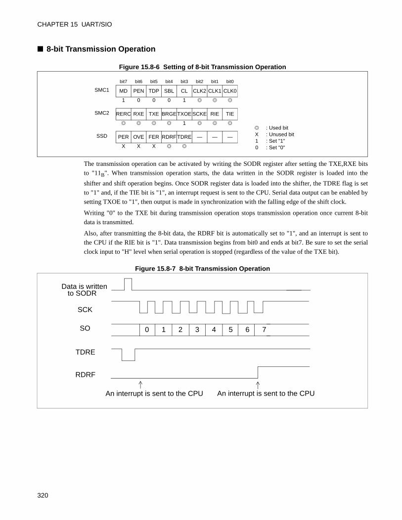
CHAPTER 15 UART/SIO
8-bit Transmission Operation
Figure 15.8-6 Setting of 8-bit Transmission Operation
The transmission operation can be activated by writing the SODR register after setting the TXE,RXE bits
to "11B". When transmission operation starts, the data written in the SODR register is loaded into the
shifter and shift operation begins. Once SODR register data is loaded into the shifter, the TDRE flag is set
to "1" and, if the TIE bit is "1", an interrupt request is sent to the CPU. Serial data output can be enabled by
setting TXOE to "1", then output is made in synchronization with the falling edge of the shift clock.
Writing "0" to the TXE bit during transmission operation stops transmission operation once current 8-bit
data is transmitted.
Also, after transmitting the 8-bit data, the RDRF bit is automatically set to "1", and an interrupt is sent to
the CPU if the RIE bit is "1". Data transmission begins from bit0 and ends at bit7. Be sure to set the serial
clock input to "H" level when serial operation is stopped (regardless of the value of the TXE bit).
Figure 15.8-7 8-bit Transmission Operation
bit7 bit6 bit5 bit4 bit3 bit2 bit1 bit0
SMC1 MD PEN TDP SBL CL CLK2 CLK1 CLK0
1 0 0 0 1
SMC2 RERC RXE TXE BRGETXOE SCKE RIE TIE
1
SSD PER OVE FER RDRF TDRE — — —
X X X
: Used bitX : Unused bit1 : Set "1"0 : Set "0"
An interrupt is sent to the CPU
0 1 2 3 4 5 6 7
to SODR
TDRE
SCK
SO
RDRF
An interrupt is sent to the CPU
Data is written
320
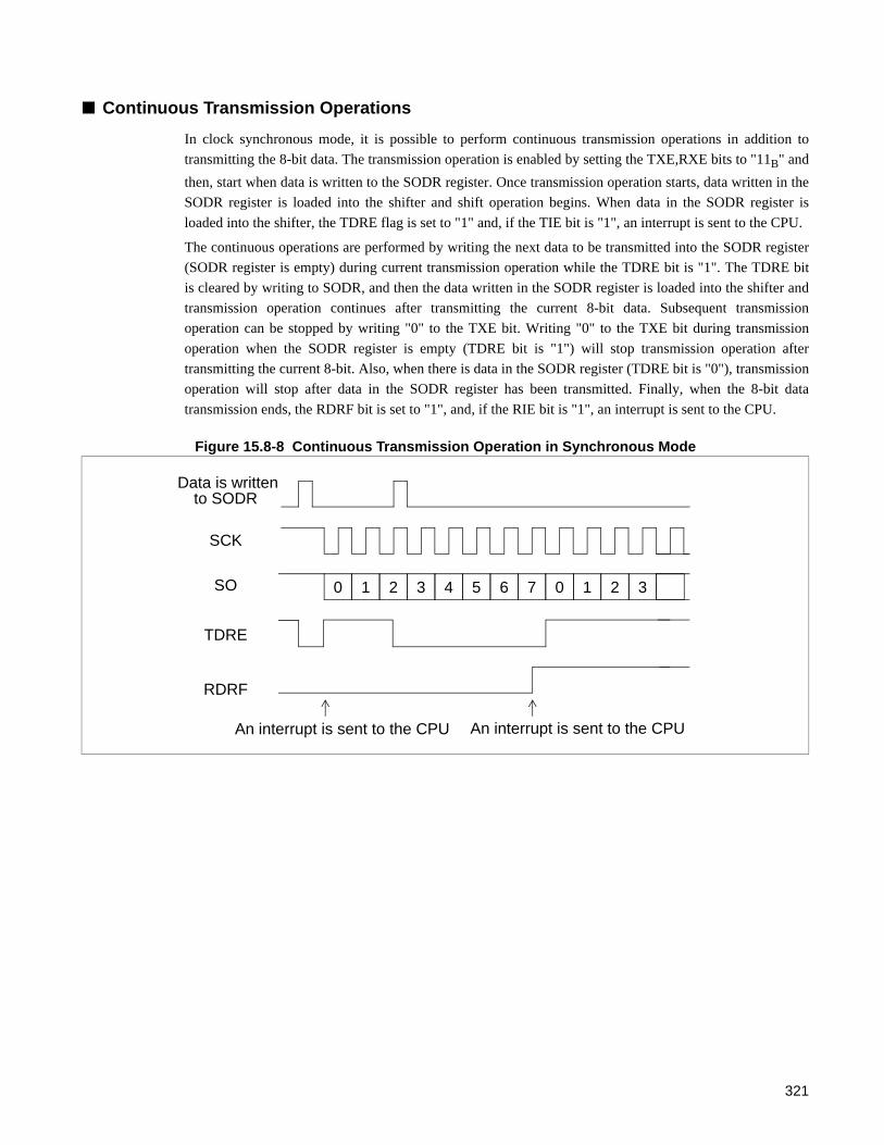
Continuous Transmission Operations
In clock synchronous mode, it is possible to perform continuous transmission operations in addition to
transmitting the 8-bit data. The transmission operation is enabled by setting the TXE,RXE bits to "11B" and
then, start when data is written to the SODR register. Once transmission operation starts, data written in the
SODR register is loaded into the shifter and shift operation begins. When data in the SODR register is
loaded into the shifter, the TDRE flag is set to "1" and, if the TIE bit is "1", an interrupt is sent to the CPU.
The continuous operations are performed by writing the next data to be transmitted into the SODR register
(SODR register is empty) during current transmission operation while the TDRE bit is "1". The TDRE bit
is cleared by writing to SODR, and then the data written in the SODR register is loaded into the shifter and
transmission operation continues after transmitting the current 8-bit data. Subsequent transmission
operation can be stopped by writing "0" to the TXE bit. Writing "0" to the TXE bit during transmission
operation when the SODR register is empty (TDRE bit is "1") will stop transmission operation after
transmitting the current 8-bit. Also, when there is data in the SODR register (TDRE bit is "0"), transmission
operation will stop after data in the SODR register has been transmitted. Finally, when the 8-bit data
transmission ends, the RDRF bit is set to "1", and, if the RIE bit is "1", an interrupt is sent to the CPU.
Figure 15.8-8 Continuous Transmission Operation in Synchronous Mode
0 1 2 3 4 5 6 7 0 1 2 3
Data is written
An interrupt is sent to the CPU An interrupt is sent to the CPU
to SODR
SCK
SO
TDRE
RDRF
321

CHAPTER 15 UART/SIO
322

CHAPTER 16BUZZER OUTPUT
This chapter describes the functions and operation of the buzzer output.
16.1 Overview of Buzzer Output
16.2 Block Diagram of Buzzer Output
16.3 Structure of Buzzer Output
16.4 Program Example for Buzzer Output
323

CHAPTER 16 BUZZER OUTPUT
16.1 Overview of Buzzer Output
The buzzer output can select from seven different output frequencies (square waves) and can be used for applications such as sounding a buzzer to confirm key input. The function uses the same output pin as the remote control transmit output.
Buzzer Output FunctionThe buzzer output function outputs a signal (square wave) suitable for applications such as sounding a
buzzer to confirm an operation.
• For buzzer output, one of seven output frequencies can be selected, or the output disabled.
• Four divide-by-n outputs are supplied from the time-base timer and three from the watch prescaler, for
selection as the buzzer output signal.
Reference:
Since divided outputs of the time-base timer and watch prescaler are fed as the buzzer output signal,the buzzer output will be affected when the signal source selected for it (time-base timer or watchprescaler) is cleared.
Note:
Since the time-base timer stops when the main clock oscillator stops (during sub clock mode), do notselect the divided output of the time-base timer as the buzzer output when sub clock mode is used.
Similarly, do not select the watch prescaler as the buzzer source in a chip in which the single clocksystem is selected.
324
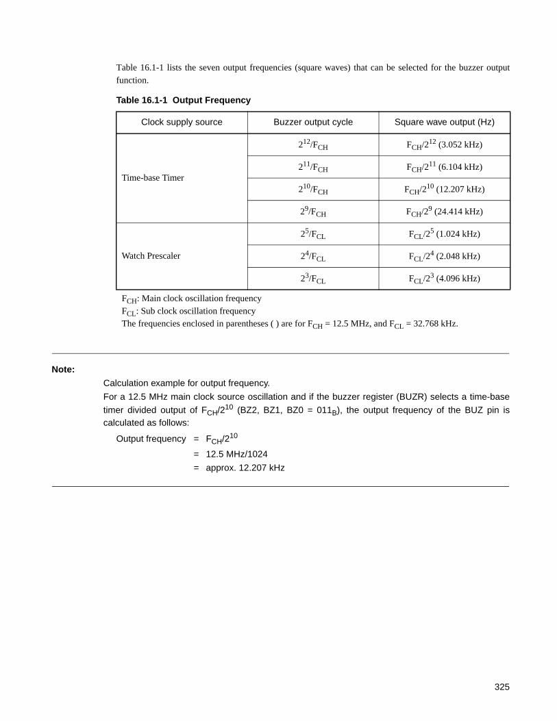
Table 16.1-1 lists the seven output frequencies (square waves) that can be selected for the buzzer output
function.
Note:
Calculation example for output frequency.
For a 12.5 MHz main clock source oscillation and if the buzzer register (BUZR) selects a time-base
timer divided output of FCH/210 (BZ2, BZ1, BZ0 = 011B), the output frequency of the BUZ pin iscalculated as follows:
Output frequency = FCH/210
= 12.5 MHz/1024
= approx. 12.207 kHz
Table 16.1-1 Output Frequency
Clock supply source Buzzer output cycle Square wave output (Hz)
Time-base Timer
212/FCH FCH/212 (3.052 kHz)
211/FCH FCH/211 (6.104 kHz)
210/FCH FCH/210 (12.207 kHz)
29/FCH FCH/29 (24.414 kHz)
Watch Prescaler
25/FCL FCL/25 (1.024 kHz)
24/FCL FCL/24 (2.048 kHz)
23/FCL FCL/23 (4.096 kHz)
FCH: Main clock oscillation frequencyFCL: Sub clock oscillation frequencyThe frequencies enclosed in parentheses ( ) are for FCH = 12.5 MHz, and FCL = 32.768 kHz.
325

CHAPTER 16 BUZZER OUTPUT
16.2 Block Diagram of Buzzer Output
The buzzer output consists of the following two blocks:• Buzzer output selector• Buzzer output register (BUZR)
Block Diagram of Buzzer Output
Figure 16.2-1 Block Diagram of Buzzer Output
Buzzer output selector
Selects one of the four frequencies output from the time-base timer or three frequencies output from the
watch prescaler.
BUZR register
The BUZR register to set the buzzer output frequency and enable buzzer output.
Buzzer output is enabled if an output frequency is specified (BUZR: BZ2, BZ1, BZ0 = other than "000B")
in the BUZR register.
BZ1BZ2 BZ0
BUZR
P07/INT27/BUZ
212/FCH
211/FCH
210/FCH
29/FCH
25/FCL
24/FCL
23/FCL
Internal data bus
SelectBuzzer output enable signal
From time-base timer
From watchprescaler
Buzzer output selector
Buzzer outputPin
FCH: Main clock oscillation frequencyFCL: Sub clock oscillation frequency
326

16.3 Structure of Buzzer Output
This section describes the pin, pin block diagram, and register of the buzzer output.
Buzzer Output PinThe buzzer output uses the P07/INT27/BUZ pin. This pin can function either as an general purpose I/O port
(P07), external interrupt input (INT27) or the buzzer output pin (BUZ).
BUZ:This pin outputs a buzzer square wave with the specified frequency.
Setting a buzzer output frequency in the buzzer output register (BZCR: BZ2, BZ1, BZ0 = other than
"000B") automatically sets the P07/BUZ pin as the BUZ pin.
Block Diagram of Buzzer Output Pin
Figure 16.3-1 Block Diagram of Buzzer Output Pin (P07/BUZ)
Buzzer Output Register
Figure 16.3-2 Buzzer Output Register
DDR
Inte
rnal
dat
a bu
s
PDR read
PDR read (for bit manipulation instructions)
PDR write
DDR write (Port direction register)
Pull-up resistorApprox. 50 kΩ
Pin
SPL: Pin state specification bit in the standby control register (STBC)
N-ch
P-ch
P-ch
Stop mode (SPL = 1)
Pull up resistorcontrol register
Output latch
Buzzer output
Buzzer output enable
Stop, watch mode
PDR (Port data register)
P07/INT27/BUZ
BUZR (Buzzer Register)Address bit7 bit6 bit5 bit4 bit3 bit2 bit1 bit0 Initial value
0040H — — — — — BZ2 BZ1 BZ0 -----000B
R/W R/W R/W
R/W : Readable/Writable
— : Undefined
327
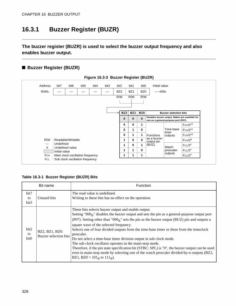
CHAPTER 16 BUZZER OUTPUT
16.3.1 Buzzer Register (BUZR)
The buzzer register (BUZR) is used to select the buzzer output frequency and also enables buzzer output.
Buzzer Register (BUZR)
Figure 16.3-3 Buzzer Register (BUZR)
Address bit7 bit6 bit5 bit4 bit3 bit2 bit1 bit0 Initial value
0040H — — — — — BZ2 BZ1 BZ0 -----000B
R/W R/W R/W
BZ2 BZ1 BZ0 Buzzer selection bits
0 0 0 Disables buzzer output. Makes pin available for use as a general-purpose port (P07).
0 0 1
Functions as a buzzer output pin (BUZ).
Time-base timer outputs
FCH/212
0 1 0 FCH/211
0 1 1 FCH/210
1 0 0 FCH/29
1 0 1Watch prescaler outputs
FCL/25
1 1 0 FCL/24
1 1 1 FCL/23
R/W : Readable/Writable— : UndefinedX : Undefined value
: Initial valueFCH : Main clock oscillation frequencyFCL : Sub clock oscillation frequency
Table 16.3-1 Buzzer Register (BUZR) Bits
Bit name Function
bit7to
bit3Unused bits
The read value is undefined.Writing to these bits has no effect on the operation.
bit2to
bit0
BZ2, BZ1, BZ0:Buzzer selection bits
These bits selects buzzer output and enable output.Setting "000B" disables the buzzer output and sets the pin as a general-purpose output port (P07). Setting other than "000B" sets the pin as the buzzer output (BUZ) pin and outputs a square wave of the selected frequency.Selects one of four divided outputs from the time-base timer or three from the timeclock prescaler.Do not select a time-base timer division output in sub clock mode.The sub clock oscillator operates in the main-stop mode.Therefore, if the pin state specification bit (STBC: SPL) is "0", the buzzer output can be used even in main-stop mode by selecting one of the watch prescaler divided-by-n outputs (BZ2, BZ1, BZ0 = 101B to 111B).
328
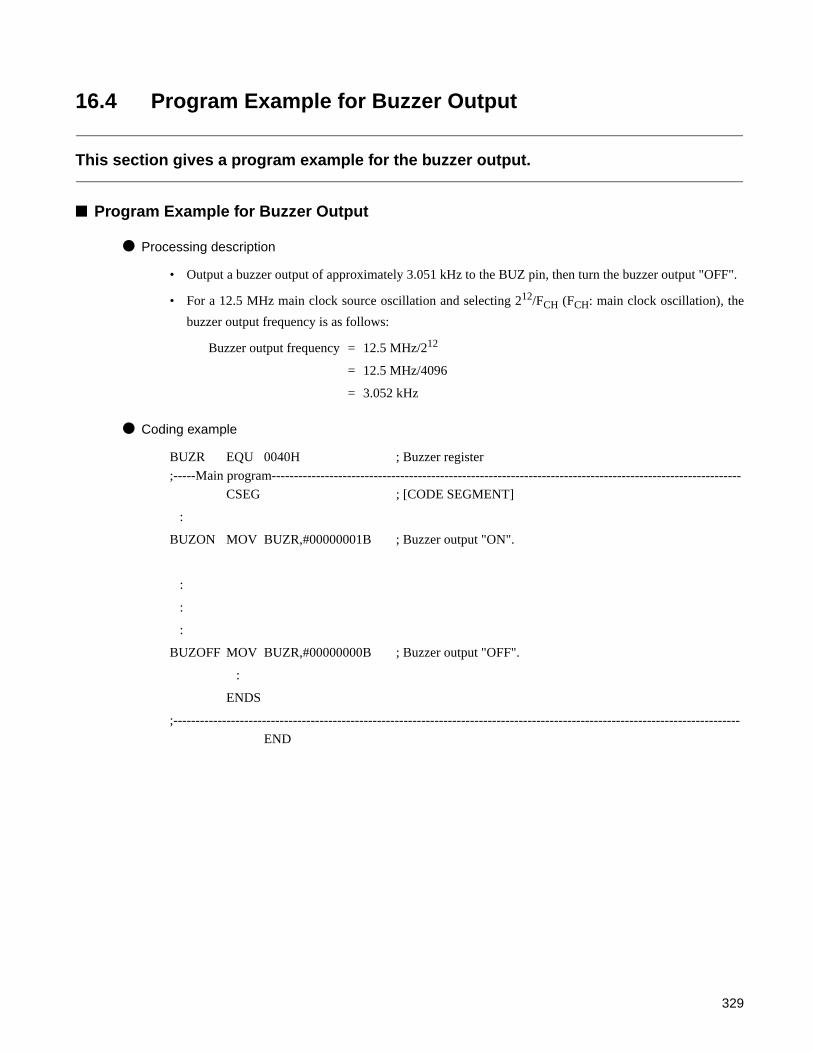
16.4 Program Example for Buzzer Output
This section gives a program example for the buzzer output.
Program Example for Buzzer Output
Processing description
• Output a buzzer output of approximately 3.051 kHz to the BUZ pin, then turn the buzzer output "OFF".
• For a 12.5 MHz main clock source oscillation and selecting 212/FCH (FCH: main clock oscillation), the
buzzer output frequency is as follows:
Buzzer output frequency = 12.5 MHz/212
= 12.5 MHz/4096
= 3.052 kHz
Coding example
BUZR EQU 0040H ; Buzzer register
;-----Main program----------------------------------------------------------------------------------------------------------
CSEG ; [CODE SEGMENT]
:
BUZON MOV BUZR,#00000001B ; Buzzer output "ON".
:
:
:
BUZOFF MOV BUZR,#00000000B ; Buzzer output "OFF".
:
ENDS
;--------------------------------------------------------------------------------------------------------------------------------
END
329

CHAPTER 16 BUZZER OUTPUT
330
CHAPTER 17LCD CONTROLLER/DRIVER
This chapter describes the functions and operation of the LCD controller/driver.
17.1 Overview of LCD Controller/Driver
17.2 Block Diagram of LCD Controller/Driver
17.3 Structure of LCD Controller/Driver
17.4 Operation of LCD Controller/Driver
17.5 Program Example for LCD Controller/Driver
331
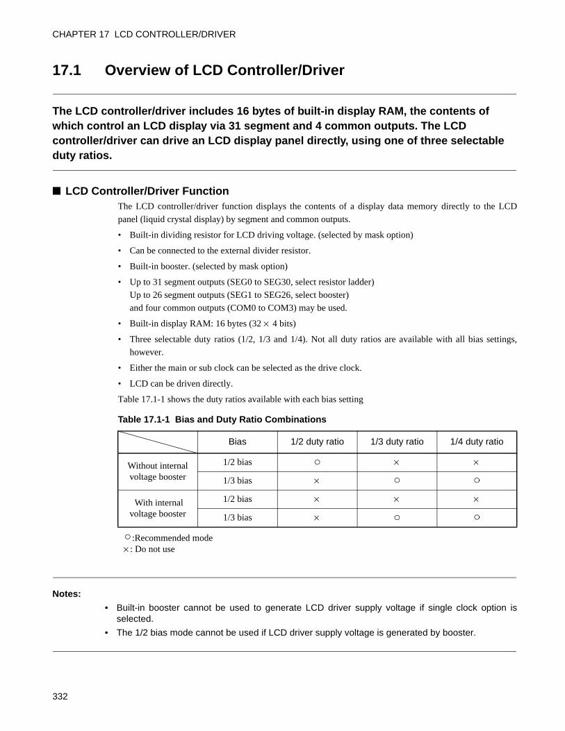
CHAPTER 17 LCD CONTROLLER/DRIVER
17.1 Overview of LCD Controller/Driver
The LCD controller/driver includes 16 bytes of built-in display RAM, the contents of which control an LCD display via 31 segment and 4 common outputs. The LCD controller/driver can drive an LCD display panel directly, using one of three selectable duty ratios.
LCD Controller/Driver FunctionThe LCD controller/driver function displays the contents of a display data memory directly to the LCD
panel (liquid crystal display) by segment and common outputs.
• Built-in dividing resistor for LCD driving voltage. (selected by mask option)
• Can be connected to the external divider resistor.
• Built-in booster. (selected by mask option)
• Up to 31 segment outputs (SEG0 to SEG30, select resistor ladder)
Up to 26 segment outputs (SEG1 to SEG26, select booster)
and four common outputs (COM0 to COM3) may be used.
• Built-in display RAM: 16 bytes (32 × 4 bits)
• Three selectable duty ratios (1/2, 1/3 and 1/4). Not all duty ratios are available with all bias settings,
however.
• Either the main or sub clock can be selected as the drive clock.
• LCD can be driven directly.
Table 17.1-1 shows the duty ratios available with each bias setting
Notes:
• Built-in booster cannot be used to generate LCD driver supply voltage if single clock option isselected.
• The 1/2 bias mode cannot be used if LCD driver supply voltage is generated by booster.
Table 17.1-1 Bias and Duty Ratio Combinations
Bias 1/2 duty ratio 1/3 duty ratio 1/4 duty ratio
Without internal voltage booster
1/2 bias × ×
1/3 bias ×
With internal voltage booster
1/2 bias × × ×
1/3 bias ×
:Recommended mode× : Do not use
332
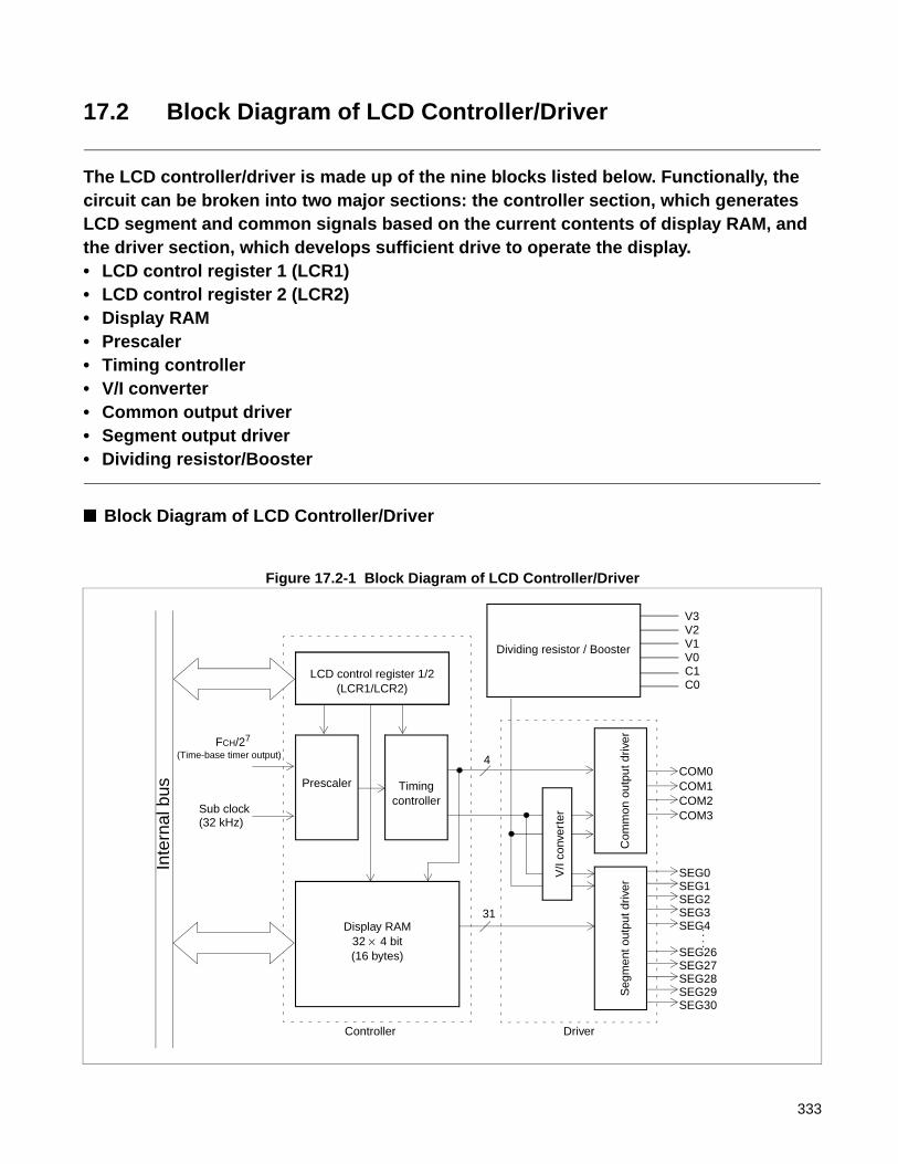
17.2 Block Diagram of LCD Controller/Driver
The LCD controller/driver is made up of the nine blocks listed below. Functionally, the circuit can be broken into two major sections: the controller section, which generates LCD segment and common signals based on the current contents of display RAM, and the driver section, which develops sufficient drive to operate the display.• LCD control register 1 (LCR1)• LCD control register 2 (LCR2)• Display RAM• Prescaler• Timing controller• V/I converter• Common output driver• Segment output driver• Dividing resistor/Booster
Block Diagram of LCD Controller/Driver
Figure 17.2-1 Block Diagram of LCD Controller/Driver
Inte
rnal
bus
LCDC control register 1/2(LCR1/LCR2)
Prescaler Timing controller
Display RAM32 × 4 bit(16 bytes)
FCH/27
(Time-base timer output)
Sub clock(32 kHz)
Com
mon
out
put d
river
Seg
men
t out
put d
river
V/I
conv
erte
r
4
31
COM0COM1COM2COM3
SEG0SEG1SEG2SEG3SEG4
SEG26SEG27SEG28SEG29SEG30
::
Controller Driver
LCD control register 1/2(LCR1/LCR2)
Dividing resistor / Booster
V3V2V1V0C1C0
333
CHAPTER 17 LCD CONTROLLER/DRIVER
LCD control register 1/2 (LCR1/LCR2)
These registers are used to select the frame clock (the clock used to generate the frame cycle), enable/
disable operation in watch mode, control the LCD driver supply voltage, select display blanking/non-
blanking, select the display mode, and select the LCD clock cycle.
Display RAM
This 32 × 4-bit block of RAM controls the segment output signals. Its contents are automatically read in
sync with the timing of the selected common signal, and output from the segment outputs at the same time
as writing the display RAM.
Prescaler
The prescaler selects settings from 2 clocks and 4 frequencies to generate the frame frequency.
Timing controller
This block controls the segment and common signals based on the frame frequency and LCR1/LCR2
register settings.
V/I converter
This circuit generates alternating current waveforms from the voltage signals it receives from the timing
controller to drive the LCD.
Common output driver
Contains the drivers for the LCD common pins.
Segment output driver
Contains the drivers for the LCD segment pins.
Dividing resistor / Booster
Generate LCD driver supply voltage.
LCD Controller/Driver Supply VoltageThe LCD driver supply voltage can be generated from booster or voltage divider. The voltage divider can
be made up of internal dividing resistors or external dividing resistors connected to the V1 to V3 pins.
334

17.2.1 LCD Controller/Driver Internal Dividing Resistors (Device without Voltage Booster)
In devices that have internal dividing resistors, the LCD driver supply voltage can be generated from an internal voltage divider. (External dividing resistors may also be used.)
Internal Dividing Resistors• The selection of internal or external diving resistors is made by the drive supply voltage control bit of
LCD control register 1 (LCR1: VSEL). VSEL = 1 connects the internal resistors. Set VSEL to "1" whenyou want to use the internal resistors only (when no external resistors are connected).
• The LCD enable is inactive when LCD operation is stopped (LCR1: MS1 = MS0 = 00B), and whenoperation is stopped (LCR1: LCEN = 0) in watch mode (STBC: TMD = 1). Pin V2 and V1 should beshorted together when using the 1/2 bias setting.
Figure 17.2-2 shows an equivalent circuit of the internal voltage divider
Figure 17.2-2 Internal Voltage Divider Equivalent Circuit
Vcc
V3
V2
V1
N-ch
P-ch 2R
N-ch
P-ch R
N-ch
P-ch R
N-ch
P-ch R
N-ch
V2
V1
V3
VSEL
Short together whenusing 1/2 bias.
MB89480 Series
LCDC enable
V1 to V3: Voltages at V1 to V3 pins.
335
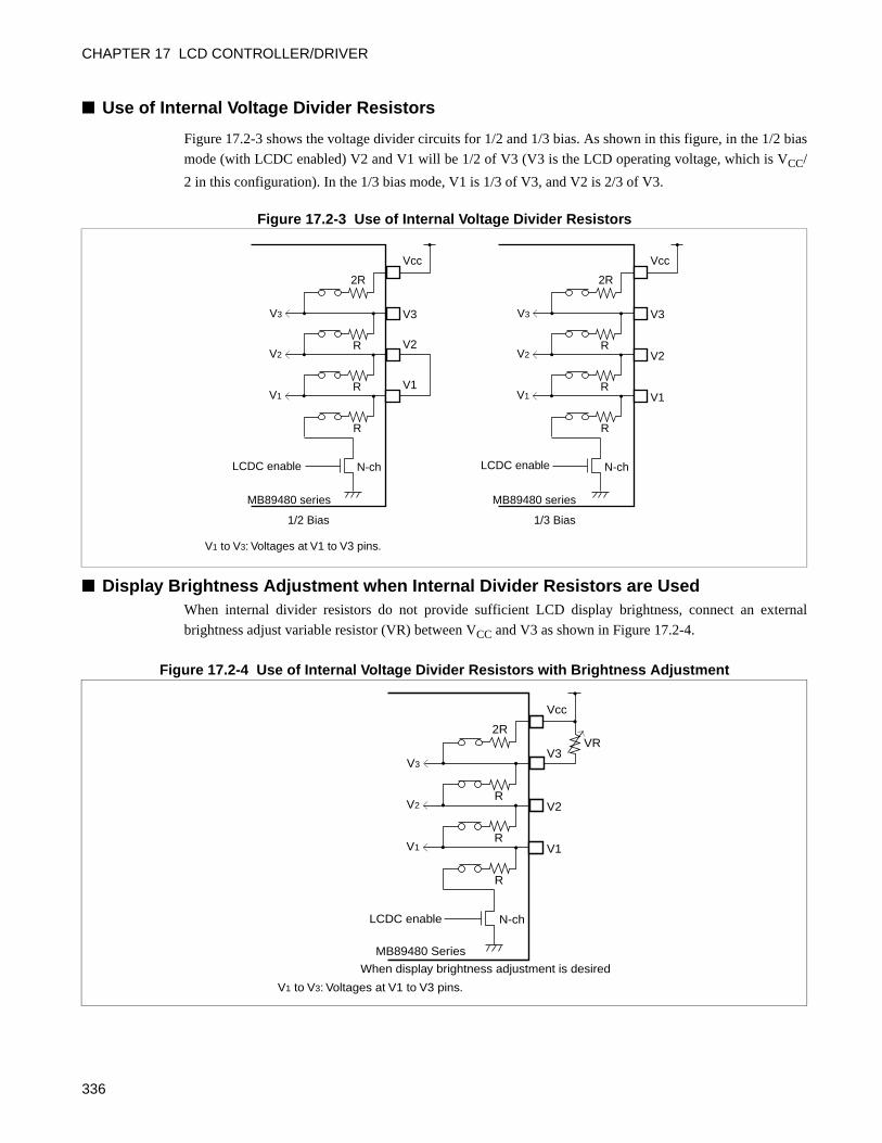
CHAPTER 17 LCD CONTROLLER/DRIVER
Use of Internal Voltage Divider Resistors
Figure 17.2-3 shows the voltage divider circuits for 1/2 and 1/3 bias. As shown in this figure, in the 1/2 bias
mode (with LCDC enabled) V2 and V1 will be 1/2 of V3 (V3 is the LCD operating voltage, which is VCC/
2 in this configuration). In the 1/3 bias mode, V1 is 1/3 of V3, and V2 is 2/3 of V3.
Figure 17.2-3 Use of Internal Voltage Divider Resistors
Display Brightness Adjustment when Internal Divider Resistors are UsedWhen internal divider resistors do not provide sufficient LCD display brightness, connect an external
brightness adjust variable resistor (VR) between VCC and V3 as shown in Figure 17.2-4.
Figure 17.2-4 Use of Internal Voltage Divider Resistors with Brightness Adjustment
2R
V3
RV2
RV1
R
Vcc
V3
V2
V1
N-chLCDC enable
MB89480 series
1/2 Bias
V1 to V3: Voltages at V1 to V3 pins.
2R
V3
RV2
RV1
R
Vcc
V3
V2
V1
N-chLCDC enable
MB89480 series
1/3 Bias
V1 to V3: Voltages at V1 to V3 pins.
2R
V3
RV2
RV1
R
Vcc
V3
V2
V1
N-ch
VR
MB89480 Series
When display brightness adjustment is desired
LCDC enable
336

Reference:
During LCD operation, the 2R internal resistance will be in the divider circuit, and VR will be inparallel with this resistor.
337

CHAPTER 17 LCD CONTROLLER/DRIVER
17.2.2 LCD Controller/Driver External Dividing Resistors (Device without Booster)
External voltage dividing resistors can also be used with devices that have internal dividing resistors. Display brightness can be adjusted by a variable resistor connected between the Vcc and V3 pins.
External Dividing ResistorsIf you do not wish to use the internal divider resistors, external voltage divider resistors can be connected at
the LCD drive voltage supply pins (V1 to V3). Figure 17.2-5 shows connections for external divider
resistors for the two biasing modes, and Table 17.2-1 lists the corresponding LCD drive voltages
Figure 17.2-5 External Voltage Divider Resistor Connections
Vcc
V3
V2
V1
VR
R
R
VLCD
MB89480 series
1/2 bias
Vcc
V3
V2
V1
VR
R
R
VLCDR
MB89480 series
1/3 bias
Table 17.2-1 LCD Drive Voltages and Biasing Modes
V3 V2 V1
1/2 bias VLCD 1/2VLCD 1/2VLCD
1/3 bias VLCD 2/3VLCD 1/3VLCD
V1 to V3: Voltages at pins V1 to V3.VLCD: LCD operating voltage
338
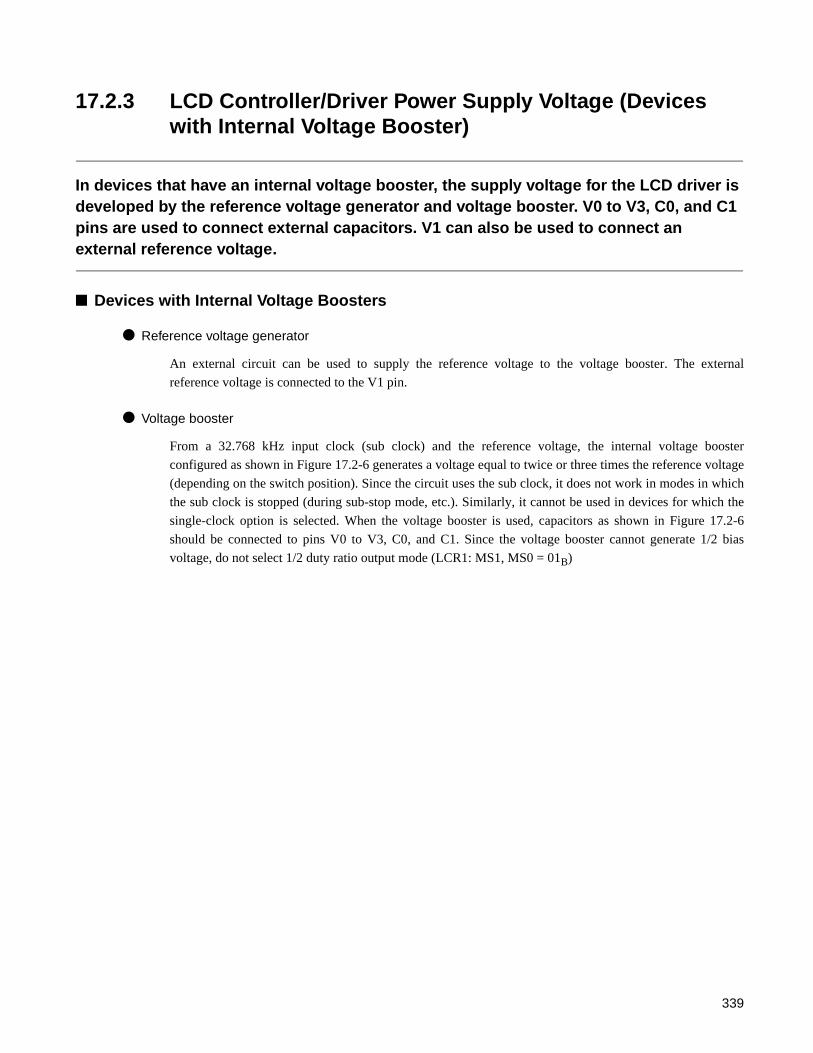
17.2.3 LCD Controller/Driver Power Supply Voltage (Devices with Internal Voltage Booster)
In devices that have an internal voltage booster, the supply voltage for the LCD driver is developed by the reference voltage generator and voltage booster. V0 to V3, C0, and C1 pins are used to connect external capacitors. V1 can also be used to connect an external reference voltage.
Devices with Internal Voltage Boosters
Reference voltage generator
An external circuit can be used to supply the reference voltage to the voltage booster. The external
reference voltage is connected to the V1 pin.
Voltage booster
From a 32.768 kHz input clock (sub clock) and the reference voltage, the internal voltage booster
configured as shown in Figure 17.2-6 generates a voltage equal to twice or three times the reference voltage
(depending on the switch position). Since the circuit uses the sub clock, it does not work in modes in which
the sub clock is stopped (during sub-stop mode, etc.). Similarly, it cannot be used in devices for which the
single-clock option is selected. When the voltage booster is used, capacitors as shown in Figure 17.2-6
should be connected to pins V0 to V3, C0, and C1. Since the voltage booster cannot generate 1/2 bias
voltage, do not select 1/2 duty ratio output mode (LCR1: MS1, MS0 = 01B)
339
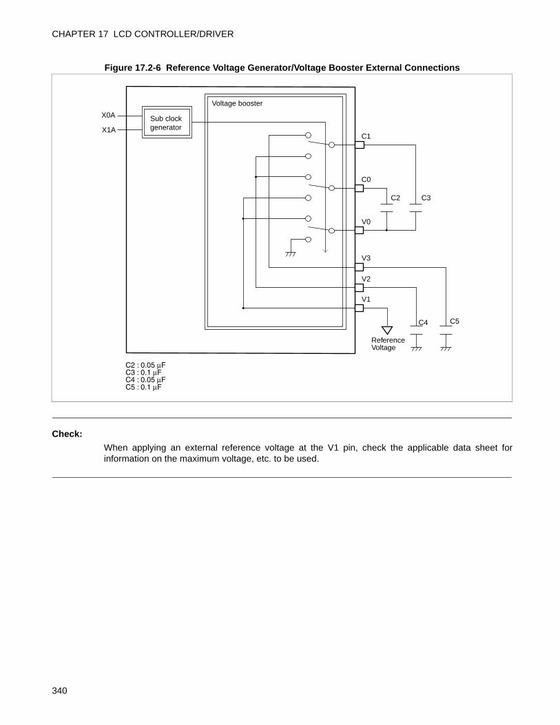
CHAPTER 17 LCD CONTROLLER/DRIVER
Figure 17.2-6 Reference Voltage Generator/Voltage Booster External Connections
Check:
When applying an external reference voltage at the V1 pin, check the applicable data sheet forinformation on the maximum voltage, etc. to be used.
C1
C0
C2 C3
V0
V3
V2
V1
C4 C5
X0A
X1A
Sub clock generator
Voltage booster
Reference Voltage
340
17.3 Structure of LCD Controller/Driver
The section describes the pins, pin block diagrams, register, and display RAM of the LCD controller/driver.
LCD Controller/Driver PinsThe LCD controller/driver uses 4 common output pins (COM0 to COM3), 31 segment output pins (SEG0
to SEG30), 2 external capacitor pins (C0 and C1), 3 LCD driving power supply pins (V1 to V3).
COM0, COM1, P31/COM2, and P32/COM3 Pins
• P30/COM2 and P31/COM3 pins can function either as output-only ports (P30 and P31) or LCDcommon output pins (COM2 and COM3). The selection is selected by the operation of the LCDC(LCR1: MS1,MS0=10B or 11B).
• When LCD display operation stop (LCR1: MS1, MS0=00B) or 1/2 duty ratio is selected (LCR1: MS1MS0=01B), P30/COM2 and P31/COM3 function as output only ports (P30 and P31).
• When 1/3 duty ratio is selected (LCR1: MS1, MS0=10B), P30/COM2 function as LCD common outputpin (COM2) and P31/COM3 function as output only port.
• When 1/4 duty ratio is selected (LCR1: MS1, MS0=11B), P30/COM2 function as LCD common outputpin (COM2) and P31/COM3 function as LCD common output pin (COM3).
Note:
When the pins are used as LCD common outputs, the corresponding port data register bits (PDR3:bit0 and bit1) should be set to "1" to turn the output transistor "off". (COM0 and COM1 are dedicatedLCD common output pins.)
SEG0/V0 to SEG7, P40/SEG8 to P47/SEG15, P50/SEG16 to P56/SEG22, and P10/SEG23 to P17/
SEG30
In device with Booster, SEG0 is used as V0. It can be used as segment output in device without booster
only. Also, when booster is selected, segment output of P14/SEG27/AN0 to P17/SEG30/AN3 will be
disabled.
P40/SEG8 to P47/SEG15, P50/SEG16 to P56/SEG22 and P10/SEG23 to P17/SEG30 pins can function
either as general-purpose I/O ports (P40 to P47, P50 to P56 and P10 to P17) or LCD segment output pins
(SEG8 to SEG15, SEG16 to SEG23, SEG24 to SEG30). The selection, is made by LCD control register 2
(LCR2: bit5 to bit0)
Note:
When these pins are used as LCD segment outputs, the corresponding port data registers (PDR1,PDR4 and PDR5) should be set to all "1s" to turn the output transistors off. (SEG0 to SEG7 arededicated LCD segment output pins.)
341

CHAPTER 17 LCD CONTROLLER/DRIVER
V1 to V3
They are the LCD driving power supply pins.
Block Diagrams of LCD Controller/Driver Pin
Figure 17.3-1 Block Diagram of LCD Controller/Driver Pin (Dedicated Common/Segment Output Pins)
Figure 17.3-2 Block Diagram of LCD Controller-Driver Pin (Dual Function Common Output Pins, P30/COM2 and P31/COM3)
Dedicated common/segment output pins
PinsCOM0, COM1SEG0*, SEG1 to SEG7
Common/segment control signal
LCD drive voltage (V3 or Vss)
LCD drive voltage (V1 or V2)
Common/segment control signal
V0 to V3: V1 to V3 pin voltages
N-ch
P-ch
P-ch
N-ch
*: In device without booster
PDR (Port data register)
Inte
rnal
dat
a bu
s
PDR read
Output latch
PDR writePins
SPL: Pin state specification bit in the standby control register (STBC)
N-chStop, watch mode (SPL = 1)
N-ch
P-ch
P-ch
N-ch
Common control signal
LCD driving voltage(V3 or Vss)
Common control signal
LCD driving voltage(V1 or V2)
P30/COM2P31/COM3
LCD output enable N-ch
342
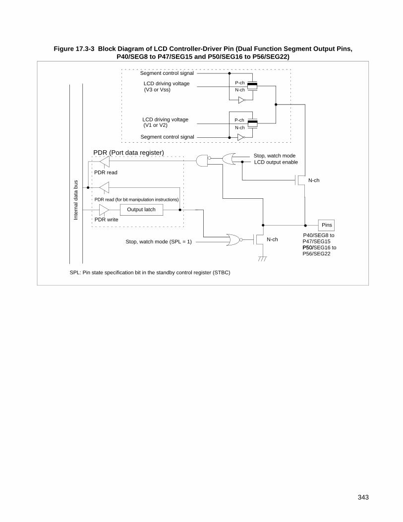
Figure 17.3-3 Block Diagram of LCD Controller-Driver Pin (Dual Function Segment Output Pins, P40/SEG8 to P47/SEG15 and P50/SEG16 to P56/SEG22)
PDR (Port data register)
Inte
rnal
dat
a bu
s
PDR read
PDR read (for bit manipulation instructions)
Output latch
PDR writePins
SPL: Pin state specification bit in the standby control register (STBC)
N-chStop, watch mode (SPL = 1)
N-ch
P-ch
P-ch
N-ch
Segment control signal
LCD driving voltage(V3 or Vss)
Segment control signal
LCD driving voltage(V1 or V2)
Stop, watch mode
P40/SEG8 to P47/SEG15P50/SEG16 toP56/SEG22P50/
LCD output enable
N-ch
343
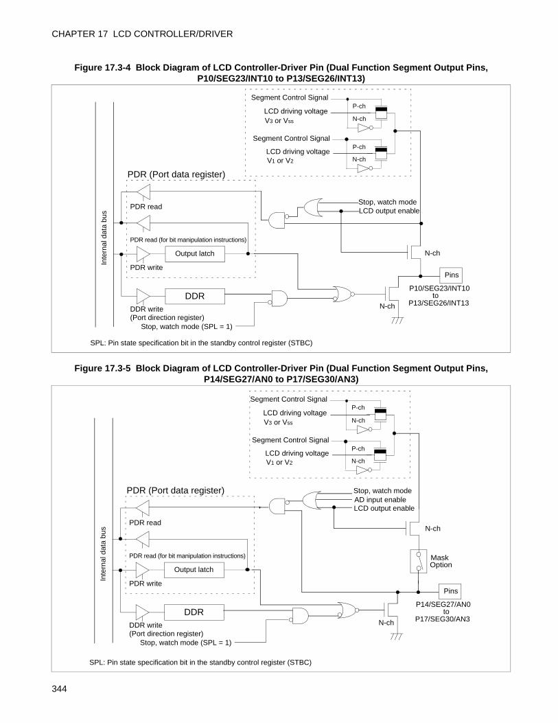
CHAPTER 17 LCD CONTROLLER/DRIVER
Figure 17.3-4 Block Diagram of LCD Controller-Driver Pin (Dual Function Segment Output Pins, P10/SEG23/INT10 to P13/SEG26/INT13)
Figure 17.3-5 Block Diagram of LCD Controller-Driver Pin (Dual Function Segment Output Pins, P14/SEG27/AN0 to P17/SEG30/AN3)
PDR (Port data register)
DDR
Inte
rnal
dat
a bu
s
PDR read
PDR read (for bit manipulation instructions)
PDR write
DDR write
Pins
SPL: Pin state specification bit in the standby control register (STBC)
N-ch
Stop, watch mode (SPL = 1)
Output latch
Stop, watch mode
(Port direction register)
Segment Control Signal
Segment Control Signal
LCD driving voltageV3 or Vss
LCD driving voltageV1 or V2
N-ch
P-ch
P-ch
N-ch
P10/SEG23/INT10
P13/SEG26/INT13to
LCD output enable
N-ch
PDR (Port data register)
DDR
Inte
rnal
dat
a bu
s
PDR read
PDR read (for bit manipulation instructions)
PDR write
DDR write
Pins
SPL: Pin state specification bit in the standby control register (STBC)
N-ch
Stop, watch mode (SPL = 1)
Output latch
Stop, watch mode AD input enable
(Port direction register)
Segment Control Signal
Segment Control Signal
LCD driving voltageV3 or Vss
LCD driving voltageV1 or V2
N-ch
P-ch
P-ch
N-ch
P14/SEG27/AN0
P17/SEG30/AN3to
LCD output enable
Mask Option
N-ch
344

Figure 17.3-6 Block Diagram of LCD Controller-Driver Pin (P24/C1/TO2, P25/C0/EC2)
Figure 17.3-7 Block Diagram of LCD Controller-Driver Pin (P26/V1/TO1, P27/V2/EC1)
PDR (Port data register)
DDR
Inte
rnal
dat
a bu
s
PDR read
PDR read (for bit manipulation instructions)
Output latch
PDR write
DDR write
Pins
* : If booster is selected by mask option, C0, C1 will connect to pin by mask option and input buffer will be disabled to avoid current leakage.
SPL: Pin state specification bit in the standby control register (STBC)
N-ch
Stop, watch mode
(Port direction register)
DDR read
Stop, watch mode Maskoption *
(SPL = 1)
Booster
Maskoption *
P24/C1/TO2P25/C0/EC2
PDR (Port data register)
DDR
Inte
rnal
dat
a bu
s
PDR read
PDR read (for bit manipulation instructions)
Output latch
PDR write
DDR write
Pins
SPL: Pin state specification bit in the standby control register (STBC)
N-ch
Stop, watch mode
(Port direction register)
DDR read
Stop, watch mode
(SPL = 1)
LCD driver/booster
LCD pin select
P26/V1/TO1P27/V2/EC1
N-ch
345
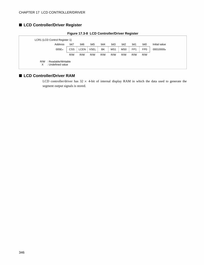
CHAPTER 17 LCD CONTROLLER/DRIVER
LCD Controller/Driver Register
Figure 17.3-8 LCD Controller/Driver Register
LCD Controller/Driver RAMLCD controller/driver has 32 × 4-bit of internal display RAM in which the data used to generate the
segment output signals is stored.
Address bit7 bit6 bit5 bit4 bit3 bit2 bit1 bit0 Initial value
005EH CSS LCEN VSEL BK MS1 MS0 FP1 FP0 00010000B
R/W R/W R/W R/W R/W R/W R/W R/W
R/W : Readable/WritableX : Undefined value
LCR1 (LCD Control Register 1)
346
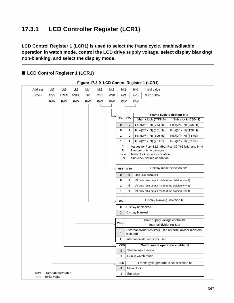
17.3.1 LCD Controller Register (LCR1)
LCD Control Register 1 (LCR1) is used to select the frame cycle, enable/disable operation in watch mode, control the LCD drive supply voltage, select display blanking/ non-blanking, and select the display mode.
LCD Control Register 1 (LCR1)
Figure 17.3-9 LCD Control Register 1 (LCR1)
Address bit7 bit6 bit5 bit4 bit3 bit2 bit1 bit0 Initial value
005EH CSS LCEN VSEL BK MS1 MS0 FP1 FP0 00010000B
R/W R/W R/W R/W R/W R/W R/W R/W
FP1 FP0Frame cycle Selection bits
Main clock (CSS=0) Sub clock (CSS=1)
0 0 FCH/(212 × N) (763 Hz) FCL/(25 × N) (256 Hz)
0 1 FCH/(213 × N) (381 Hz) FCL/(26 × N) (128 Hz)
1 0 FCH/(214 × N) (190 Hz) FCL/(27 × N) (64 Hz)
1 1 FCH/(215 × N) (95 Hz) FCL/(28 × N) (32 Hz)
( ) : Values for FCH=12.5 MHz, FCL=32.768 kHz, and N=4N : Number of time divisions
FCH : Main clock source oscillationFCL : Sub clock source oscillation
MS1 MS0 Display mode selection bits
0 0 Stop LCD operation
0 1 1/2 duty ratio output mode (time division N = 2)
1 0 1/3 duty ratio output mode (time division N = 3)
1 1 1/4 duty ratio output mode (time division N = 4)
BK Display blanking selection bit
0 Display unblanked
1 Display blanked
VSELDrive supply voltage control bit
Internal divider resistor
0External divider resistors used (internal divider resistors isolated)
1 Internal divider resistors used.
LCEN Watch mode operation enable bit
0 Stop in watch mode
1 Run in watch mode
CSS Frame cycle generate clock selection bit
0 Main clock
1 Sub clockR/W : Readable/Writable: Initial value
347
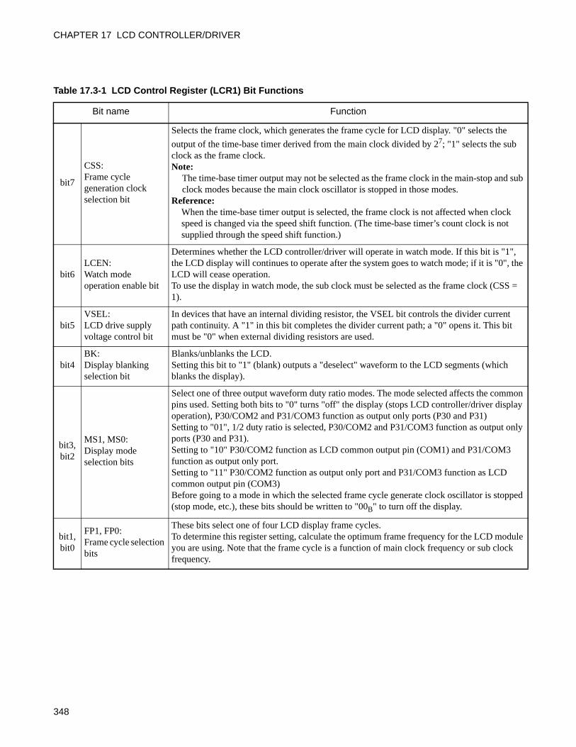
CHAPTER 17 LCD CONTROLLER/DRIVER
Table 17.3-1 LCD Control Register (LCR1) Bit Functions
Bit name Function
bit7
CSS: Frame cycle generation clock selection bit
Selects the frame clock, which generates the frame cycle for LCD display. "0" selects the
output of the time-base timer derived from the main clock divided by 27; "1" selects the sub clock as the frame clock.Note:
The time-base timer output may not be selected as the frame clock in the main-stop and sub clock modes because the main clock oscillator is stopped in those modes.
Reference:When the time-base timer output is selected, the frame clock is not affected when clock speed is changed via the speed shift function. (The time-base timer’s count clock is not supplied through the speed shift function.)
bit6LCEN: Watch mode operation enable bit
Determines whether the LCD controller/driver will operate in watch mode. If this bit is "1", the LCD display will continues to operate after the system goes to watch mode; if it is "0", the LCD will cease operation.To use the display in watch mode, the sub clock must be selected as the frame clock (CSS = 1).
bit5VSEL: LCD drive supply voltage control bit
In devices that have an internal dividing resistor, the VSEL bit controls the divider current path continuity. A "1" in this bit completes the divider current path; a "0" opens it. This bit must be "0" when external dividing resistors are used.
bit4BK: Display blanking selection bit
Blanks/unblanks the LCD.Setting this bit to "1" (blank) outputs a "deselect" waveform to the LCD segments (which blanks the display).
bit3,bit2
MS1, MS0: Display mode selection bits
Select one of three output waveform duty ratio modes. The mode selected affects the common pins used. Setting both bits to "0" turns "off" the display (stops LCD controller/driver display operation), P30/COM2 and P31/COM3 function as output only ports (P30 and P31)Setting to "01", 1/2 duty ratio is selected, P30/COM2 and P31/COM3 function as output only ports (P30 and P31).Setting to "10" P30/COM2 function as LCD common output pin (COM1) and P31/COM3 function as output only port.Setting to "11" P30/COM2 function as output only port and P31/COM3 function as LCD common output pin (COM3)Before going to a mode in which the selected frame cycle generate clock oscillator is stopped (stop mode, etc.), these bits should be written to "00B" to turn off the display.
bit1,bit0
FP1, FP0: Frame cycle selection bits
These bits select one of four LCD display frame cycles.To determine this register setting, calculate the optimum frame frequency for the LCD module you are using. Note that the frame cycle is a function of main clock frequency or sub clock frequency.
348

17.3.2 LCD Controller Register 2 (LCR2)
LCD Control Register 2 (LCR2) is used to switch between segment and port. Select a function from general-purpose I/O port or segment output.
LCD Control Register 2 (LCR2)
Figure 17.3-10 LCD Control Register 1 (LCR2)
Address bit7 bit6 bit5 bit4 bit3 bit2 bit1 bit0 Initial value
005FH RESV PSEL SEG14 SEG13 SEG12 SEG11 SEG10 SEG00 00000000B
R/W R/W R/W R/W R/W R/W R/W
SEG00 Segment Output Selection bit
0 Select as ports (P54 to P56)
1 Select as segment output (SEG20 to SEG22)
SEG10 Segment Output Selection bit
0 Select as ports (P50 to P53)
1 Select as segment output (SEG16 to SEG19)
SEG11 Segment Output Selection bit
0 Select as ports (P44 to P47)
1 Select as segment output (SEG12 to SEG15)
SEG12 Segment Output Selection bit
0 Select as ports (P40 to P43)
1 Select as segment output (SEG8 to SEG11)
SEG13 Segment Output Selection bit
0 Select as ports (P14 to P17)
1 Select as segment output (SEG27 to SEG30)
SEG14 Segment Output Selection bit
0 Select as ports (P10 to P13)
1 Select as segment output (SEG23 to SEG26)
PSEL LCD Voltage Supply Selection bit
0 Select as LCD power supply pins (V1 and V2)
1 Select as port pins (P26, P27)
RESV Reserved bit
Always write "0" to this bitR/W : Readable/Writable— : Undefined value
: Initial value
349
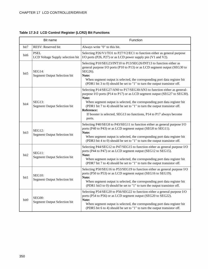
CHAPTER 17 LCD CONTROLLER/DRIVER
Table 17.3-2 LCD Control Register (LCR2) Bit Functions
Bit name Function
bit7 RESV: Reserved bit Always write "0" to this bit.
bit6PSELLCD Voltage Supply selection bit
Selecting P26/V1/TO1 to P27/V2/EC1 to function either as general purpose I/O ports (P26, P27) or as LCD power supply pin (V1 and V2).
bit5SEG14: Segment Output Selection bit
Selecting P10/SEG23/INT10 to P13/SEG26/INT13 to function either as general purpose I/O ports (P10 to P13) or as LCD segment output (SEG30 to SEG26).Note:
When segment output is selected, the corresponding port data register bit (PDR1 bit 3 to 0) should be set to "1" to turn the output transistor off.
bit4SEG13: Segment Output Selection bit
Selecting P14/SEG27/AN0 to P17/SEG30/AN3 to function either as general-purpose I/O ports (P14 to P17) or as LCD segment output (SEG27 to SEG30).Note:
When segment output is selected, the corresponding port data register bit (PDR1 bit 7 to 4) should be set to "1" to turn the output transistor off.
Reference: If booster is selected, SEG13 no functions, P14 to P17 always become ports.
bit3SEG12: Segment Output Selection bit
Selecting P40/SEG8 to P43/SEG11 to function either as general purpose I/O ports (P40 to P43) or as LCD segment output (SEG8 to SEG11).Note:
When segment output is selected, the corresponding port data register bit (PDR3 bit 4 to 0) should be set to "1" to turn the output transistor off.
bit2SEG11: Segment Output Selection bit
Selecting P44/SEG12 to P47/SEG15 to function either as general purpose I/O ports (P44 to P47) or as LCD segment output (SEG12 to SEG15).Note:
When segment output is selected, the corresponding port data register bit (PDR7 bit 7 to 4) should be set to "1" to turn the output transistor off.
bit1SEG10: Segment Output Selection bit
Selecting P50/SEG16 to P53/SEG19 to function either as general purpose I/O ports (P50 to P53) or as LCD segment output (SEG16 to SEG19).Note:
When segment output is selected, the corresponding port data register bit (PDR1 bit3 to 0) should be set to "1" to turn the output transistor off.
bit0SEG00: Segment Output Selection bit
Selecting P54/SEG20 to P56/SEG22 to function either a general purpose I/O ports (P54 to P56) or as LCD segment output (SEG20 to SEG22).Note:
When segment output is selected, the corresponding port data register bit (PDR5 bit 6 to 4) should be set to "1" to turn the output transistor off.
350

17.3.3 Display RAM
Display RAM consists of 32 × 4-bit (16 bytes) of display data memory used to generate the segment output signals.
Display RAM and Output PinsThe contents of display RAM are automatically read out and output via the segment outputs in sync with
the selected common signal timing. A "1" bit is converted to a "select" (display on) voltage and a "0" to a
"deselect" (display off) voltage. Since the operation of the LCD is not directly related to the operation of
the CPU, display RAM read/write timing can be set by the user. The SEG8 to SEG30 pins that are not
dedicated segment outputs may be used as general-purpose I/O port pins, and the RAM that goes with those
pins may be used as regular RAM. (See Table 17.3-3.)
Table 17.3-4 shows the relationship between duty ratio mode, common outputs, and display RAM.
Figure 17.3-11 shows which display RAM bits are associated with each segment and common output pin.
Figure 17.3-11 Segment/Common Output Pins and Corresponding Display RAMAddress
0060H
bit3 bit2 bit1 bit0 SEG0
bit7 bit6 bit5 bit4 SEG1
0061H
bit3 bit2 bit1 bit0 SEG2
bit7 bit6 bit5 bit4 SEG3
0062H
bit3 bit2 bit1 bit0 SEG4
bit7 bit6 bit5 bit4 SEG5
0063H
bit3 bit2 bit1 bit0 SEG6
bit7 bit6 bit5 bit4 SEG7
0064H
bit3 bit2 bit1 bit0 SEG8
bit7 bit6 bit5 bit4 SEG9
0065H
bit3 bit2 bit1 bit0 SEG10
bit7 bit6 bit5 bit4 SEG11
0066H
bit3 bit2 bit1 bit0 SEG12
bit7 bit6 bit5 bit4 SEG13
0067H
bit3 bit2 bit1 bit0 SEG14
bit7 bit6 bit5 bit4 SEG15
0068H
bit3 bit2 bit1 bit0 SEG16
bit7 bit6 bit5 bit4 SEG17
0069H
bit3 bit2 bit1 bit0 SEG18
bit7 bit6 bit5 bit4 SEG19
006AH
bit3 bit2 bit1 bit0 SEG20
bit7 bit6 bit5 bit4 SEG21
006BH
bit3 bit2 bit1 bit0 SEG22
bit7 bit6 bit5 bit4 SEG23
006CH
bit3 bit2 bit1 bit0 SEG24
bit7 bit6 bit5 bit4 SEG25
006DH
bit3 bit2 bit1 bit0 SEG26
bit7 bit6 bit5 bit4 SEG27
006EH
bit3 bit2 bit1 bit0 SEG28
bit7 bit6 bit5 bit4 SEG29
006FH
bit3 bit2 bit1 bit0 SEG30
- - - -
COM3 COM2 COM1 COM0
Pins SEG8 to SEG15 share pins with Port 4 (P40 to P47).
Pins SEG16 to SEG22 share pins with Port 5 (P50 to P56).
RAM area and common pins used in 1/2 duty ratio modeRAM area and common pins used in 1/3 duty ratio modeRAM area and common pins used in 1/4 duty ratio mode
Pins SEG23 to SEG30 share pins with Port 1 (P10 to P17).
351
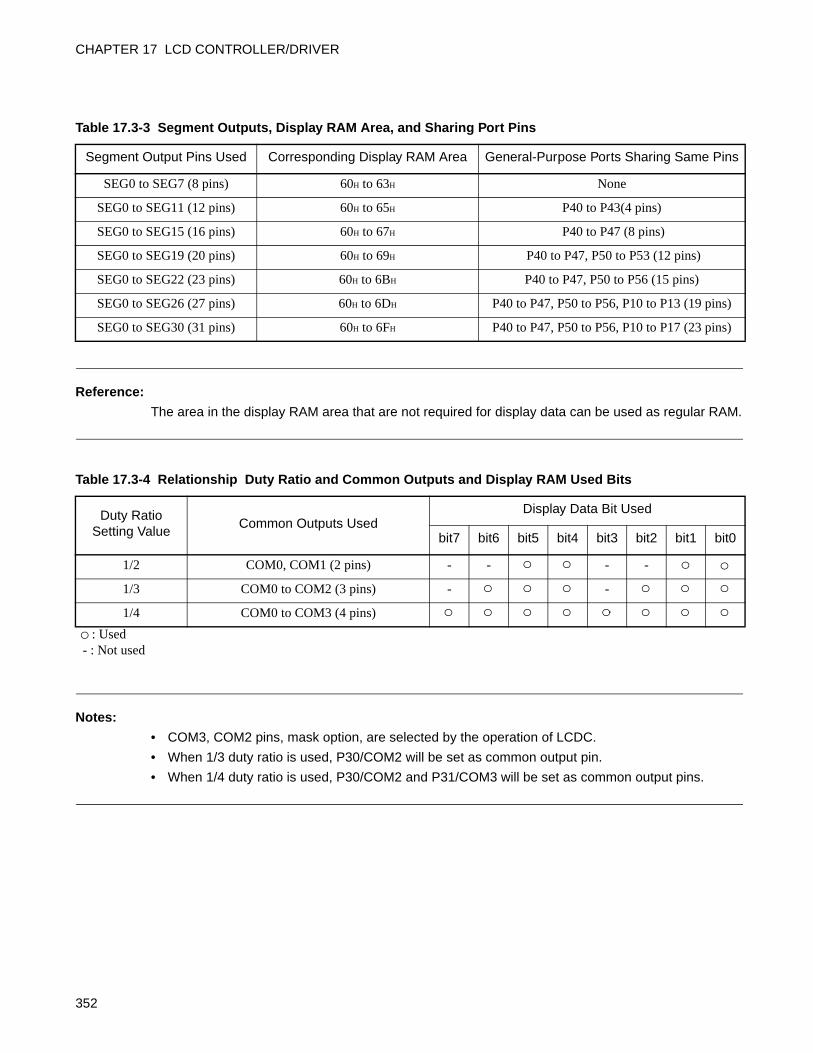
CHAPTER 17 LCD CONTROLLER/DRIVER
Reference:
The area in the display RAM area that are not required for display data can be used as regular RAM.
Notes:
• COM3, COM2 pins, mask option, are selected by the operation of LCDC.
• When 1/3 duty ratio is used, P30/COM2 will be set as common output pin.
• When 1/4 duty ratio is used, P30/COM2 and P31/COM3 will be set as common output pins.
Table 17.3-3 Segment Outputs, Display RAM Area, and Sharing Port Pins
Segment Output Pins Used Corresponding Display RAM Area General-Purpose Ports Sharing Same Pins
SEG0 to SEG7 (8 pins) 60H to 63H None
SEG0 to SEG11 (12 pins) 60H to 65H P40 to P43(4 pins)
SEG0 to SEG15 (16 pins) 60H to 67H P40 to P47 (8 pins)
SEG0 to SEG19 (20 pins) 60H to 69H P40 to P47, P50 to P53 (12 pins)
SEG0 to SEG22 (23 pins) 60H to 6BH P40 to P47, P50 to P56 (15 pins)
SEG0 to SEG26 (27 pins) 60H to 6DH P40 to P47, P50 to P56, P10 to P13 (19 pins)
SEG0 to SEG30 (31 pins) 60H to 6FH P40 to P47, P50 to P56, P10 to P17 (23 pins)
Table 17.3-4 Relationship Duty Ratio and Common Outputs and Display RAM Used Bits
Duty Ratio Setting Value
Common Outputs UsedDisplay Data Bit Used
bit7 bit6 bit5 bit4 bit3 bit2 bit1 bit0
1/2 COM0, COM1 (2 pins) - - - -
1/3 COM0 to COM2 (3 pins) - -
1/4 COM0 to COM3 (4 pins)
: Used - : Not used
352

17.4 Operation of LCD Controller/Driver
The LCD controller/driver provides the necessary control and drive for an LCD display.
Operation of LCD Controller/DriverFigure 17.4-1 shows the settings required to operate the LCD display
Figure 17.4-1 LCD Controller/Driver Settings
• Once the above settings have been made, if the selected clock for frame cycle generation is running,LCD panel driving waveforms reflecting the contents of display RAM will be output at the segment andcommon output pins (COM0 to COM3 and SEG0 to SEG30).
• Although the clock for frame period generation can be switched even while the LCD is displaying data,the display may flicker when the switching occurs. This can be avoided by temporarily blanking thedisplay (LCR1: BK = 1), etc. while switching.
• The display driving output is a two-frame a.c. waveform for which the bias level and display duty cycleis selected by settings.
• When LCD display operation is stopped (LCR1: MS1 = MS0 = 00B), and during reset, only COM1,COM0 and SEG0 to SEG7 output pins will go to "L" level COM2/P30, COM3/P31 and SEG8/P40 toSEG30/P17 will be high impedance.
Note:
If the selected frame cycle generate clock were to stop while the LCD display is operating, the circuitthat converts the waveform from d.c. to a.c. would also stop, causing a d.c. voltage to be applied tothe liquid crystal cells. The LCD display must be therefore be stopped before the clock is stopped.The conditions under which the main clock (time-base timer) and sub clock are stopped are afunction of the clock mode and standby mode. Also note that when the time-base timer is selectedas the frame clock source (LCR1: CSS = 0), clearing the time-base timer will affect the frame cycle.
Reference:
See "APPENDIX E MB89480/480L Series Pin States".
bit7 bit6 bit5 bit4 bit3 bit2 bit1 bit0
LCR1 CSS LCEN VSEL BK MS1 MS0 FP1 FP0
0
Display RAM060H to 06FH
Display data : Used bit1 : Set "1".0 : Set "0".
Other than “00H”
353

CHAPTER 17 LCD CONTROLLER/DRIVER
LCD Driving Waveforms
It is characteristic of LCDs that applying d.c. drive to the panel can cause electrochemical degradation of
the material used in the LCD cells. For this reason, the LCD controller/driver includes a circuit to convert
the original driving waveform to a two-frame a.c. output waveform (zero d.c. bias) to drive the LCD. There
are three types of output waveform:
• 1/2 bias, 1/2 duty ratio output waveform
• 1/3 bias, 1/3 duty ratio output waveform
• 1/3 bias, 1/4 duty ratio output waveform
354
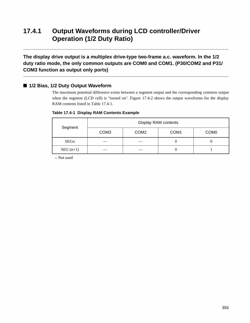
17.4.1 Output Waveforms during LCD controller/Driver Operation (1/2 Duty Ratio)
The display drive output is a multiplex drive-type two-frame a.c. waveform. In the 1/2 duty ratio mode, the only common outputs are COM0 and COM1. (P30/COM2 and P31/COM3 function as output only ports)
1/2 Bias, 1/2 Duty Output WaveformThe maximum potential difference exists between a segment output and the corresponding common output
when the segment (LCD cell) is "turned on". Figure 17.4-2 shows the output waveforms for the display
RAM contents listed in Table 17.4-1.
Table 17.4-1 Display RAM Contents Example
SegmentDisplay RAM contents
COM3 COM2 COM1 COM0
SEGn — — 0 0
SEG (n+1) — — 0 1
-: Not used
355
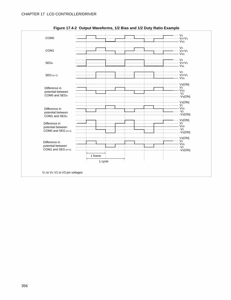
CHAPTER 17 LCD CONTROLLER/DRIVER
Figure 17.4-2 Output Waveforms, 1/2 Bias and 1/2 Duty Ratio Example
V3V2=V1VSS
V3V2=V1VSS
V3(ON)V2VSS-V2-V3(ON)
V3(ON)V2VSS-V2-V3(ON)
V3(ON)V2VSS-V2-V3(ON)
V3(ON)V2VSS-V2-V3(ON)
COM0
COM1
V3V2=V1VSs
V3V2=V1VSS
SEGn
SEG (n+1)
Difference in potential between COM0 and SEGn
Difference in potential between COM1 and SEGn
Difference in potential between COM0 and SEG (n+1)
Difference in potential between COM1 and SEG (n+1)
1 frame
1 cycle
V1 to V3: V1 to V3 pin voltages
356
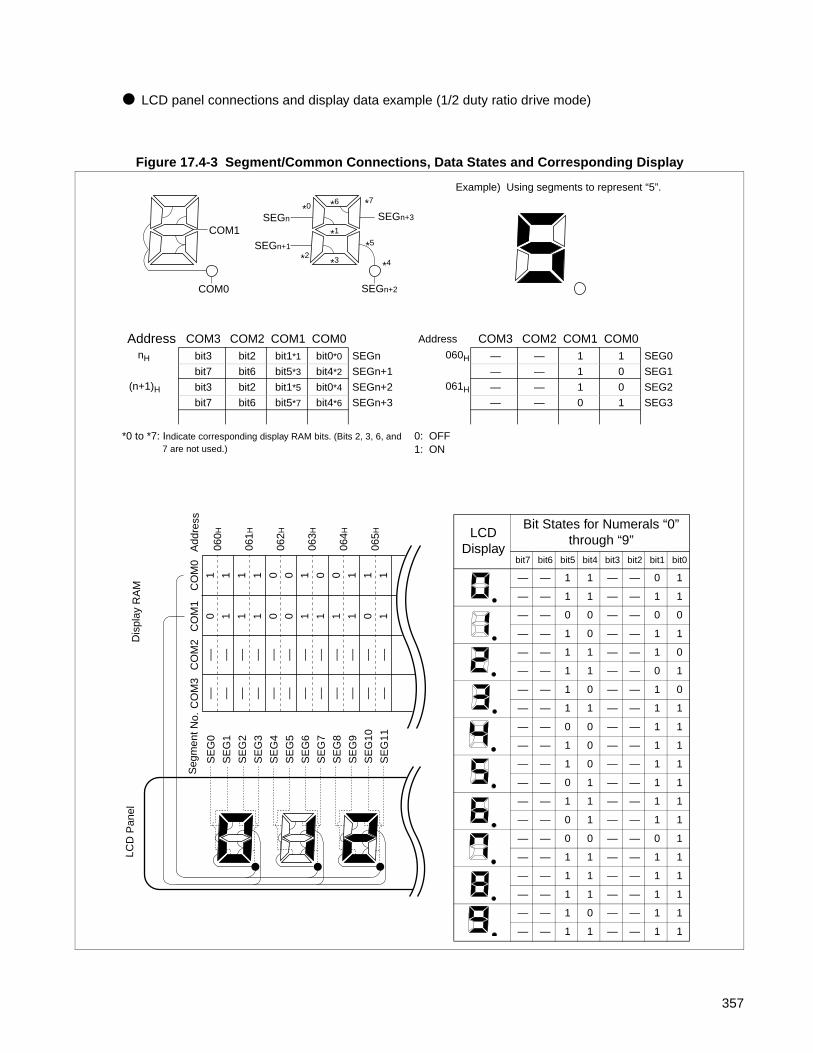
LCD panel connections and display data example (1/2 duty ratio drive mode)
Figure 17.4-3 Segment/Common Connections, Data States and Corresponding Display
COM1
COM0
SEGn+3
SEGn+2
SEGn+1
SEGn
*7*0
*5
*4*2
*6
*1
*3
SE
G0
SE
G1
SE
G2
SE
G3
SE
G4
SE
G5
SE
G6
SE
G7
SE
G8
SE
G9
SE
G10
SE
G11
CO
M3
–– –– –– –– –– –– –– –– –– –– –– ––
CO
M2
–– –– –– –– –– –– –– –– –– –– –– ––
CO
M1
0 1 1 1 0 0 1 1 1 1 0 1
CO
M0
1 1 1 1 0 0 1 0 0 1 1 1
060H
061H
062H
063H
064H
065H
LC
D P
anel
Dis
play
RA
M
Add
ress
Seg
men
t No.
*0 to *7: Indicate corresponding display RAM bits. (Bits 2, 3, 6, and 7 are not used.)
Address COM3 COM2 COM1 COM0 nH bit3 bit2 bit1*1 bit0*0 SEGn
bit7 bit6 bit5*3 bit4*2 SEGn+1 (n+1)H bit3 bit2 bit1*5 bit0*4 SEGn+2
bit7 bit6 bit5*7 bit4*6 SEGn+3
0: OFF1: ON
Address COM3 COM2 COM1 COM0060H — — 1 1 SEG0
— — 1 0 SEG1061H — — 1 0 SEG2
— — 0 1 SEG3
LCD Display
Bit States for Numerals “0” through “9”
bit7 bit6 bit5 bit4 bit3 bit2 bit1 bit0
— — 1 1 — — 0 1
— — 1 1 — — 1 1
— — 0 0 — — 0 0
— — 1 0 — — 1 1
— — 1 1 — — 1 0
— — 1 1 — — 0 1
— — 1 0 — — 1 0
— — 1 1 — — 1 1
— — 0 0 — — 1 1
— — 1 0 — — 1 1
— — 1 0 — — 1 1
— — 0 1 — — 1 1
— — 1 1 — — 1 1
— — 0 1 — — 1 1
— — 0 0 — — 0 1
— — 1 1 — — 1 1
— — 1 1 — — 1 1
— — 1 1 — — 1 1
— — 1 0 — — 1 1
— — 1 1 — — 1 1
Example) Using segments to represent “5”.
357
CHAPTER 17 LCD CONTROLLER/DRIVER
17.4.2 Output Waveforms during LCD Controller/Driver Operation (1/3 Duty Ratio)
In the 1/3 duty ratio mode, the COM0, COM1 and COM2 outputs are used by the display. (P31/COM3 function as output only port)
Output Waveforms during LCD Controller/Driver Operation (1/3 Duty Ratio)
1/3 bias, 1/3 duty output waveform
Table 17.4-2 Display RAM Contents Example
SegmentDisplay RAM contents
COM3 COM2 COM1 COM0
SEGn — 1 0 0
SEG (n+1) — 1 0 1
-: Not used
358

Figure 17.4-4 Output Waveforms, 1/3 Bias and 1/3 Duty Ratio Example
V3V2V1VSS
V3V2V1VSS
V3V2V1VSS
V3V2V1V0=VSS
V3V2V1VSS
V3(ON)V2V1VSS-V1-V2-V3(ON)V3(ON)V2V1VSS-V1-V2-V3(ON)V3(ON)V2V1VSS-V1-V2-V3(ON)V3(ON)V2V1VSS-V1-V2-V3(ON)V3(ON)V2V1VSS-V1-V2-V3(ON)V3(ON)V2V1VSS-V1-V2-V3(ON)
COM0
COM1
COM2
SEGn
SEG (n+1)
Difference in potential between COM0 and SEGn
Difference in potential between COM1 and SEGn
Difference in potential between COM2 and SEGn
Difference in potential between COM0 and SEG (n+1)
Difference in potential between COM1 and SEG (n+1)
Difference in potential between COM2 and SEG (n+1)
1 frame
1 cycleV0 to V3: V0 to V3 pin voltages
359
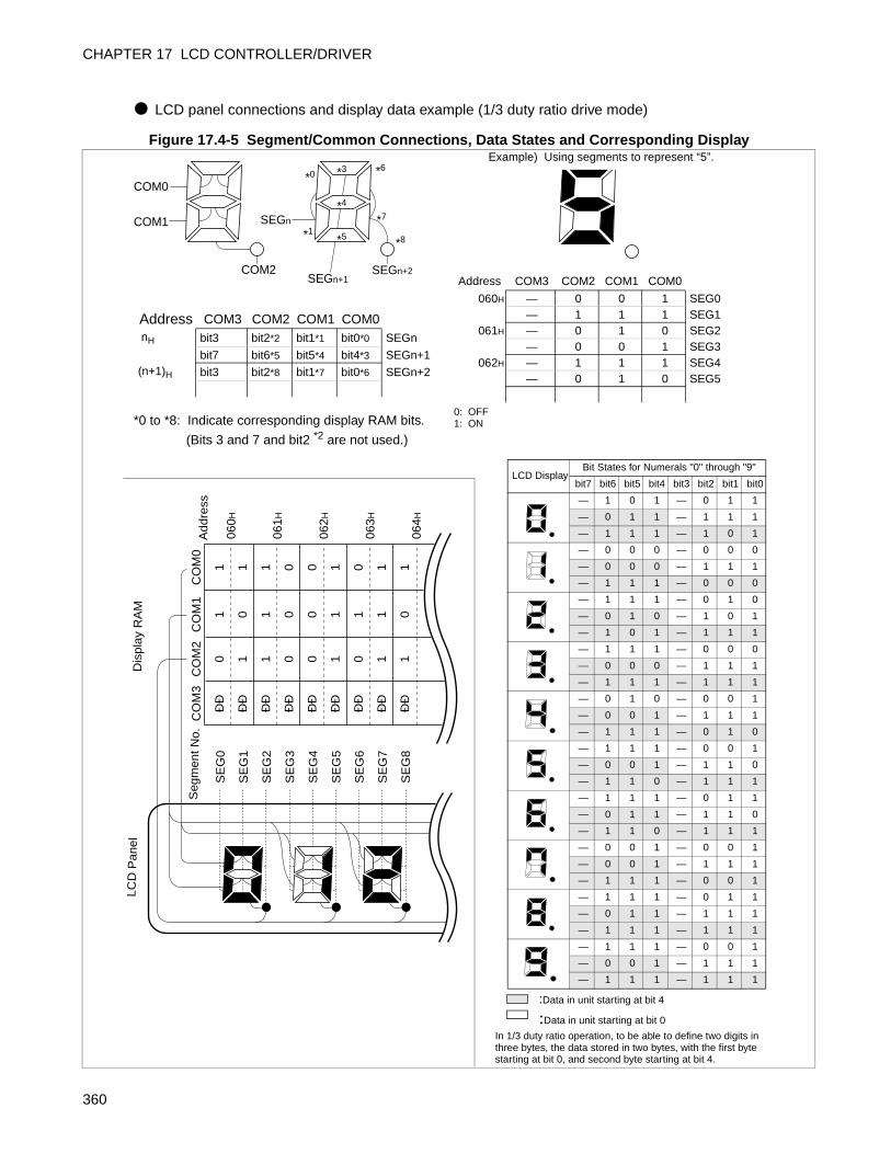
CHAPTER 17 LCD CONTROLLER/DRIVER
LCD panel connections and display data example (1/3 duty ratio drive mode)
Figure 17.4-5 Segment/Common Connections, Data States and Corresponding Display
COM2 SEGn+2
SEGn
*6*0
*7
*8*1
*3
*4
*5
SE
G0
SE
G1
SE
G2
SE
G3
SE
G4
SE
G5
SE
G6
SE
G7
SE
G8
CO
M3
ÐÐ
ÐÐ
ÐÐ
ÐÐ
ÐÐ
ÐÐ
ÐÐ
ÐÐ
ÐÐ
CO
M2
0 1 1 0 0 1 0 1 1
CO
M1
1 0 1 0 0 1 1 1 0
CO
M0
1 1 1 0 0 1 0 1 1
060H
061H
062H
063H
064H
COM0
COM1
SEGn+1
Dis
play
RA
M
Seg
men
t No.
LCD
Pan
el
Add
ress
*0 to *8: Indicate corresponding display RAM bits.
(Bits 3 and 7 and bit2 *2 are not used.)
Address COM3 COM2 COM1 COM0 nH bit3 bit2*2 bit1*1 bit0*0 SEGn
bit7 bit6*5 bit5*4 bit4*3 SEGn+1(n+1)H bit3 bit2*8 bit1*7 bit0*6 SEGn+2
0: OFF1: ON
Address COM3 COM2 COM1 COM0
060H — 0 0 1 SEG0— 1 1 1 SEG1
061H — 0 1 0 SEG2— 0 0 1 SEG3
062H — 1 1 1 SEG4— 0 1 0 SEG5
:Data in unit starting at bit 4
:Data in unit starting at bit 0
In 1/3 duty ratio operation, to be able to define two digits in three bytes, the data stored in two bytes, with the first byte starting at bit 0, and second byte starting at bit 4.
LCD DisplayBit States for Numerals "0" through "9"
bit7 bit6 bit5 bit4 bit3 bit2 bit1 bit0
— 1 0 1 — 0 1 1
— 0 1 1 — 1 1 1
— 1 1 1 — 1 0 1
— 0 0 0 — 0 0 0
— 0 0 0 — 1 1 1
— 1 1 1 — 0 0 0
— 1 1 1 — 0 1 0
— 0 1 0 — 1 0 1
— 1 0 1 — 1 1 1
— 1 1 1 — 0 0 0
— 0 0 0 — 1 1 1
— 1 1 1 — 1 1 1
— 0 1 0 — 0 0 1
— 0 0 1 — 1 1 1
— 1 1 1 — 0 1 0
— 1 1 1 — 0 0 1
— 0 0 1 — 1 1 0
— 1 1 0 — 1 1 1
— 1 1 1 — 0 1 1
— 0 1 1 — 1 1 0
— 1 1 0 — 1 1 1
— 0 0 1 — 0 0 1
— 0 0 1 — 1 1 1
— 1 1 1 — 0 0 1
— 1 1 1 — 0 1 1
— 0 1 1 — 1 1 1
— 1 1 1 — 1 1 1
— 1 1 1 — 0 0 1
— 0 0 1 — 1 1 1
— 1 1 1 — 1 1 1
Example) Using segments to represent “5”.
360
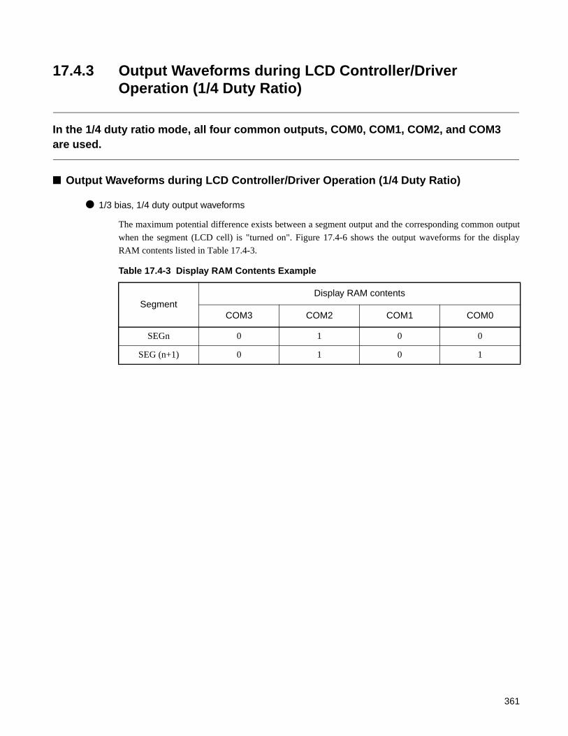
17.4.3 Output Waveforms during LCD Controller/Driver Operation (1/4 Duty Ratio)
In the 1/4 duty ratio mode, all four common outputs, COM0, COM1, COM2, and COM3 are used.
Output Waveforms during LCD Controller/Driver Operation (1/4 Duty Ratio)
1/3 bias, 1/4 duty output waveforms
The maximum potential difference exists between a segment output and the corresponding common output
when the segment (LCD cell) is "turned on". Figure 17.4-6 shows the output waveforms for the display
RAM contents listed in Table 17.4-3.
Table 17.4-3 Display RAM Contents Example
SegmentDisplay RAM contents
COM3 COM2 COM1 COM0
SEGn 0 1 0 0
SEG (n+1) 0 1 0 1
361
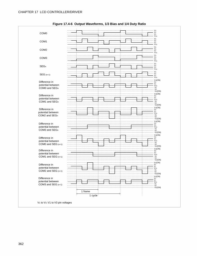
CHAPTER 17 LCD CONTROLLER/DRIVER
Figure 17.4-6 Output Waveforms, 1/3 Bias and 1/4 Duty Ratio
V3V2V1VSS
V3V2V1VSS
V3V2V1VSS
V3V3V3VSS
V3V2V1VSS
V3V2V1VSS
V3(ON)V2V1VSS-V1-V2-V3(ON)V3(ON)V2V1VSS-V1-V2-V3(ON)V3(ON)V2V1VSS-V1-V2-V3(ON)V3(ON)V2V1VSS-V1-V2-V3(ON)V3(ON)V2V1VSS-V1-V2-V3(ON)V3(ON)V2V1VSS-V1-V2-V3(ON)
COM0
COM1
COM2
COM3
SEGn
SEG (n+1)
V3(ON)V2V1VSS-V1-V2-V3(ON)
V3(ON)V2V1VSS-V1-V2-V3(ON)
Difference in potential between COM0 and SEGn
Difference in potential between COM1 and SEGn
Difference in potential between COM2 and SEGn
Difference in potential between COM3 and SEGn
Difference in potential between COM0 and SEG (n+1)
Difference in potential between COM1 and SEG (n+1)
Difference in potential between COM2 and SEG (n+1)
Difference in potential between COM3 and SEG (n+1)
1 frame
1 cycle
V1 to V3: V1 to V3 pin voltages
362

8-segment LCD panel connections and Display data (1/4 duty ratio drive mode)
Figure 17.4-7 Segment/Common Connections, Data States and Corresponding Display
COM2
SEGn
*7*0
*3
*6*1
*4
*5
*2
SE
G0
SE
G1
SE
G2
SE
G3
SE
G4
SE
G5
SE
G6
SE
G7
CO
M3
1 1 1 1 0 1 1 1
CO
M2
1 1 0 1 1 1 1 1
CO
M1
1 0 0 0 1 1 0 1
CO
M0
1 1 0 0 0 1 0 1
060 H
061H
062H
063H
COM0
COM1
SEGn+1
COM3
LCD
Pan
elD
ispl
ay R
AM
Add
ress
Seg
men
t No.
*0 to *7: Indicate corresponding display RAM bits.
Address COM3 COM2 COM1 COM0 nH bit3*3 bit2*2 bit1*1 bit0*0 SEGn
bit7*7 bit6*6 bit5*5 bit4*4 SEGn+1
0: OFF1: ON
Address COM3 COM2 COM1 COM0060H 1 1 0 1 SEG0
0 0 1 1 SEG1
LCD Display
Bit States for Numerals "0" through "9"
bit7 bit6 bit5 bit4 bit3 bit2 bit1 bit0
1 1 0 1 1 1 1 1
1 1 0 0 1 0 0 0
1 1 1 1 0 1 1 0
1 1 1 1 1 1 0 0
1 1 1 0 1 0 0 1
0 1 1 1 1 1 0 1
0 1 1 1 1 1 1 1
1 1 0 1 1 0 0 1
1 1 1 1 1 1 1 1
1 1 1 1 1 1 0 1
Example) Using segments to represent “5”.
363
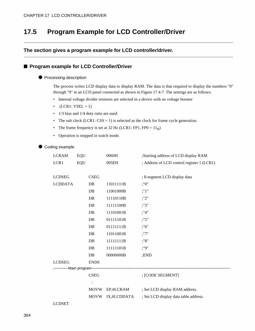
CHAPTER 17 LCD CONTROLLER/DRIVER
17.5 Program Example for LCD Controller/Driver
The section gives a program example for LCD controller/driver.
Program example for LCD Controller/Driver
Processing description
The process writes LCD display data to display RAM. The data is that required to display the numbers "0"
through "9" in an LCD panel connected as shown in Figure 17.4-7. The settings are as follows:
• Internal voltage divider resistors are selected in a device with no voltage booster
• (LCR1: VSEL = 1)
• 1/3 bias and 1/4 duty ratio are used.
• The sub clock (LCR1: CSS = 1) is selected as the clock for frame cycle generation.
• The frame frequency is set at 32 Hz (LCR1: FP1, FP0 = 11B)
• Operation is stopped in watch mode.
Coding example
LCRAM EQU 0060H ;Starting address of LCD display RAM
LCR1 EQU 005EH ; Address of LCD control register 1 (LCR1)
LCDSEG CSEG ; 8-segment LCD display data
LCDDATA DB 11011111B ;"0"
DB 11001000B ;"1"
DB 11110110B ;"2"
DB 11111100B ;"3"
DB 11101001B ;"4"
DB 01111101B ;"5"
DB 01111111B ;"6"
DB 11011001B ;"7"
DB 11111111B ;"8"
DB 11111101B ;"9"
DB 00000000B ;END
LCDSEG ENDS
;----------Main program----------------------------------------------------------------------------------------------------
CSEG ; [CODE SEGMENT]
:
MOVW EP,#LCRAM ; Set LCD display RAM address.
MOVW IX,#LCDDATA ; Set LCD display data table address.
LCDSET
364
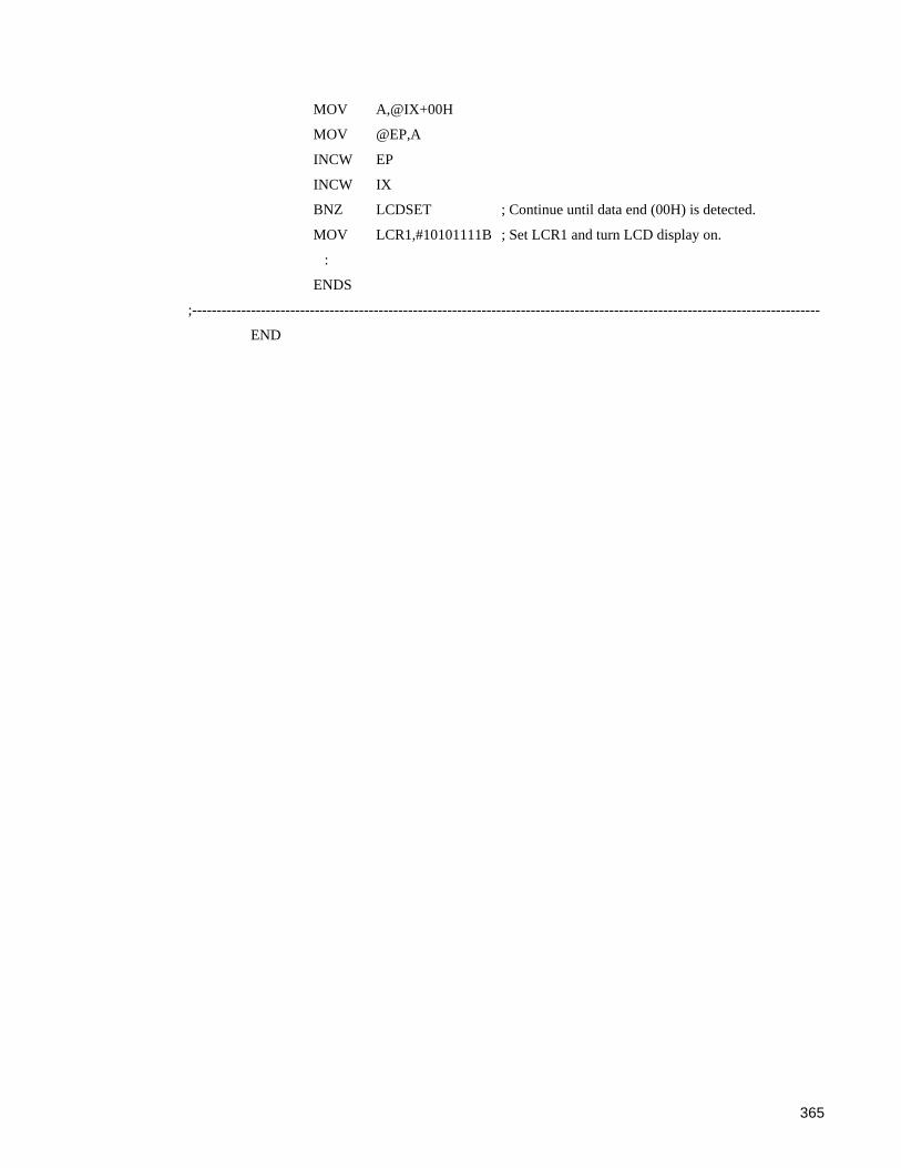
MOV A,@IX+00H
MOV @EP,A
INCW EP
INCW IX
BNZ LCDSET ; Continue until data end (00H) is detected.
MOV LCR1,#10101111B ; Set LCR1 and turn LCD display on.
:
ENDS
;--------------------------------------------------------------------------------------------------------------------------------
END
365

CHAPTER 17 LCD CONTROLLER/DRIVER
366

APPENDIX
The appendices provide I/O map, instruction list and other information.
APPENDIX A I/O MAP
APPENDIX B Instructions
B.1 Addressing
B.2 Special Instructions
B.3 F2MC-8L Instructions
B.4 Instruction Map
B.5 Bit Manipulation Instructions (SETB, CLRB)
APPENDIX C Mask Options
APPENDIX D Programming Specifications for one-time PROM and EPROM Microcontrollers
D.1 Programming One-time PROM Microcontroller with serial programmer
D.2 Programming One-time PROM Microcontroller parallel programmer
D.3 Programming EPROM for Piggyback/Evaluation Device
APPENDIX E MB89480/480L Series Pin States
367

APPENDIX A I/O MAP
APPENDIX A I/O MAP
Table A-1 lists the addresses of the registers used by the internal peripheral functions of the MB89480/480L series.
I/O map
Table A-1 I/O Map (1 / 3)
Address Register name Register Description Read/Write Initial value
00H PDR0 Port 0 data register R/W XXXXXXXXB
01H DDR0 Port 0 data direction register W* 00000000B
02H PDR1 Port 1 data register R/W XXXXXXXXB
03H DDR1 Port 1 data direction register W* 00000000B
04H PDR2 Port 2 data register R/W 00000000B
05H (Reserved)
06H DDR2 Port 2 data direction register R/W 00000000B
07H SYCC System clock control register R/W X-1MM100B
08H STBC Standby control register R/W 00010XXXB
09H WDTC Watchdog timer control register W* 0---XXXXB
0AH TBTC Time-base timer control register R/W 00---000B
0BH WPCR Watch prescaler control register R/W 00--0000B
0CH PDR3 Port 3 data register R/W ------11B
0DH (Reserved)
0EH RSFR Reset flag register R XXXX----B
0FH (Reserved)
10H PDR4 Port 4 data register R/W 11111111B
11H (Reserved)
12H PDR5 Port 5 data register R/W X1111111B
13H (Reserved)
14H to 1FH (Reserved)
20H SMC1 UART/SIO mode control register 1 R/W 00000000B
21H SMC2 UART/SIO mode control register 2 R/W 00000000B
22H SRC UART/SIO rate control register R/W XXXXXXXXB
368

23H SSD UART/SIO status/data register R 00001---B
24H SIDR/SODR UART/SIO data register R/W XXXXXXXXB
25H EIC1 External interrupt control register 1 R/W 00000000B
26H EIC2 External interrupt control register 2 R/W 00000000B
27H EIE2 External interrupt 2 enable register R/W 00000000B
28H EIF2 External interrupt 2 flag register R/W -------0B
29H to 2BH (Reserved)
2CH ADC1 A/D control register 1 R/W -0000000B
2DH ADC2 A/D control register 2 R/W -0000001B
2EH ADDH A/D data register (Upper byte) R ------XXB
2FH ADDL A/D data register (Lower byte) R XXXXXXXXB
30H ADEN A/D input enable register R/W 1111----B
31H PCR1 PWC control register 1 R/W 0-0--000B
32H PCR2 PWC control register 2 R/W 00000000B
33H PLBR PWC reload buffer register R/W XXXXXXXXB
34H CNTR PWM timer control register R/W 0-000000B
35H COMR PWM timer compare register W* XXXXXXXXB
36H T22CR Timer 22 control register R/W 000000X0B
37H T21CR Timer 21 control register R/W 000000X0B
38H T22DR Timer 22 data register R/W XXXXXXXXB
39H T21DR Timer 21 data register R/W XXXXXXXXB
3AH T12CR Timer 12 control register R/W 000000X0B
3BH T11CR Timer 11 control register R/W 000000X0B
3CH T12DR Timer 12 data register R/W XXXXXXXXB
3DH T11DR Timer 11 data register R/W XXXXXXXXB
3EH PPGC1 PPG control register 1 R/W 00000000B
3FH PPGC2 PPG control register 2 R/W 0-000000B
40H BUZR Buzzer control register R/W -----000B
41H to 5DH (Reserved)
5EH LCR1 LCD control register 1 R/W 00010000B
5FH LCR2 LCD control register 2 R/W -0000000B
Table A-1 I/O Map (2 / 3)
Address Register name Register Description Read/Write Initial value
369
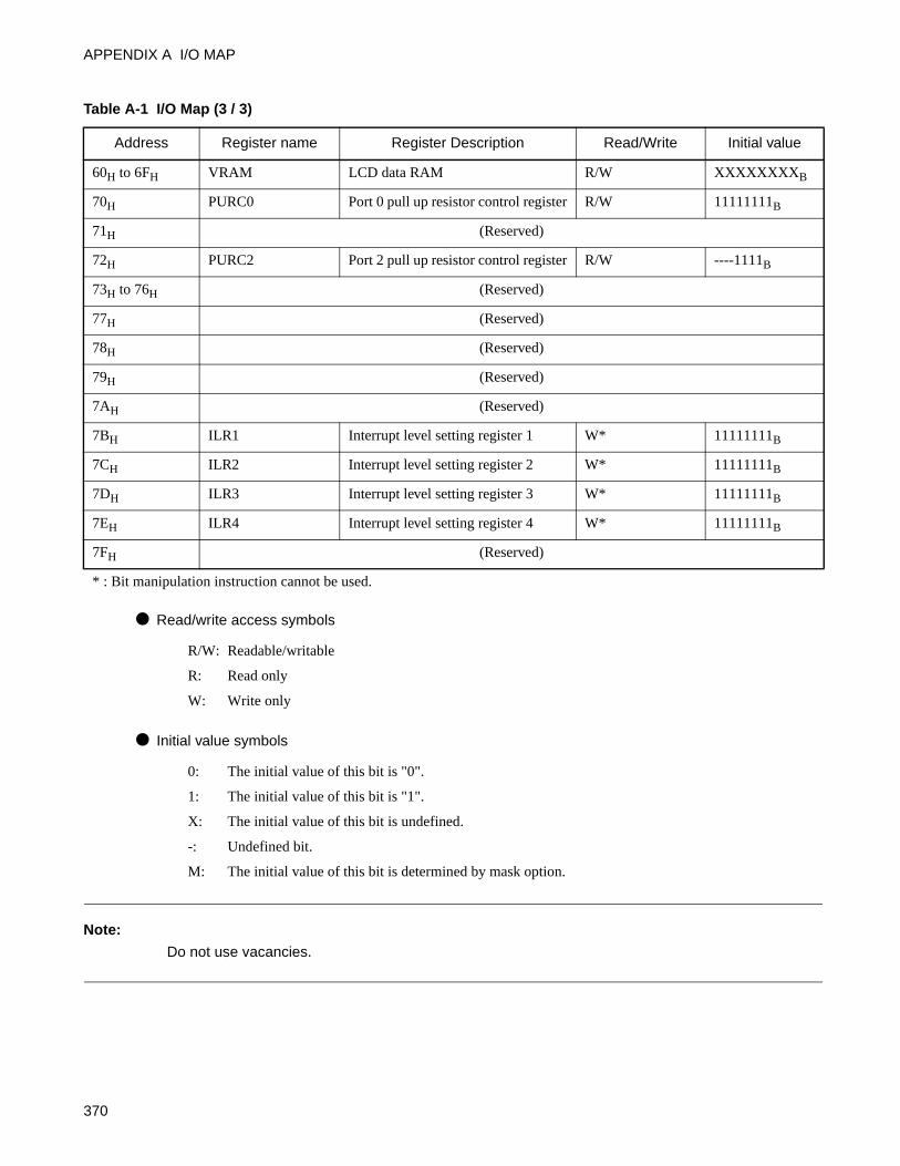
APPENDIX A I/O MAP
Read/write access symbols
R/W: Readable/writable
R: Read only
W: Write only
Initial value symbols
0: The initial value of this bit is "0".
1: The initial value of this bit is "1".
X: The initial value of this bit is undefined.
-: Undefined bit.
M: The initial value of this bit is determined by mask option.
Note:
Do not use vacancies.
60H to 6FH VRAM LCD data RAM R/W XXXXXXXXB
70H PURC0 Port 0 pull up resistor control register R/W 11111111B
71H (Reserved)
72H PURC2 Port 2 pull up resistor control register R/W ----1111B
73H to 76H (Reserved)
77H (Reserved)
78H (Reserved)
79H (Reserved)
7AH (Reserved)
7BH ILR1 Interrupt level setting register 1 W* 11111111B
7CH ILR2 Interrupt level setting register 2 W* 11111111B
7DH ILR3 Interrupt level setting register 3 W* 11111111B
7EH ILR4 Interrupt level setting register 4 W* 11111111B
7FH (Reserved)
* : Bit manipulation instruction cannot be used.
Table A-1 I/O Map (3 / 3)
Address Register name Register Description Read/Write Initial value
370

APPENDIX B Instructions
This appendix describes the F2MC-8L instruction set.
Instruction List SymbolsTable B-1 lists the meaning of the symbols and Table B-2 lists the meanings of the columns used in "B.3
F2MC-8L Instructions".
Table B-1 Instruction List Symbols (1 / 2)
Symbol Meaning
dir Direct address (8 bits)
off Offset (8 bits)
ext Extended address (16 bits)
#vct Vector table number (3 bits)
#d8 Immediate data (8 bits)
#d16 Immediate data (16 bits)
dir: b Bit direct address (8:3 bits)
rel Branch relative address (8 bits)
@ Register indirect (Example: @A, @IX, @EP)
A Accumulator A (Whether its length is 8 or 16 bits is determined by the instruction in use.)
AH Upper 8 bits of the accumulator A (8 bits)
AL Lower 8 bits of the accumulator A (8 bits)
T Temporary accumulator T (Whether its length is 8 or 16 bits is determined by the instruction in use.)
TH Upper 8 bits of the temporary accumulator T (8 bits)
TL Lower 8 bits of the temporary accumulator T (8 bits)
IX Index register IX (16 bits)
EP Extra pointer EP (16 bits)
PC Program counter PC (16 bits)
SP Stack pointer SP (16 bits)
PS Program status PS (16 bits)
dr Accumulator A or index register IX (16 bits)
CCR Condition code register CCR (8 bits)
RP Register bank pointer RP (5 bits)
371
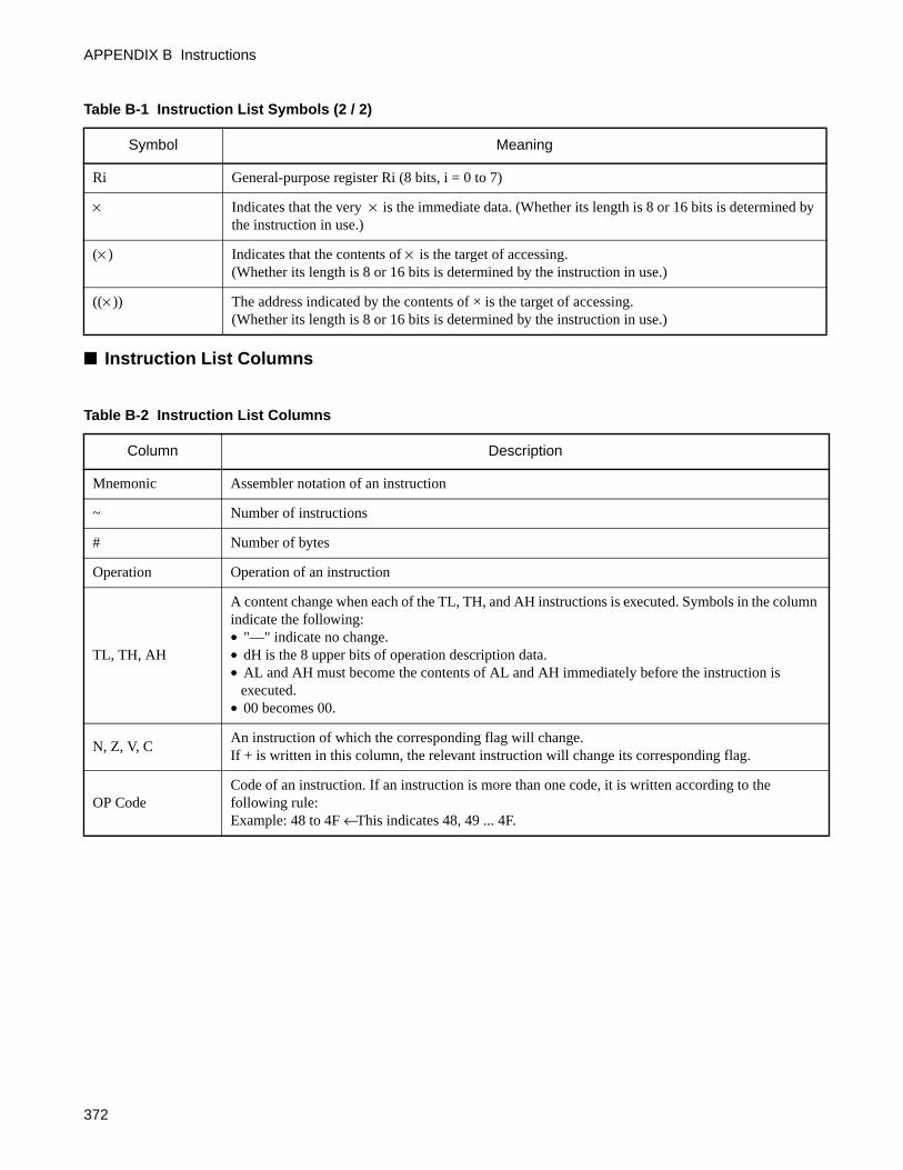
APPENDIX B Instructions
Instruction List Columns
Ri General-purpose register Ri (8 bits, i = 0 to 7)
× Indicates that the very × is the immediate data. (Whether its length is 8 or 16 bits is determined by the instruction in use.)
(× ) Indicates that the contents of × is the target of accessing.(Whether its length is 8 or 16 bits is determined by the instruction in use.)
((× )) The address indicated by the contents of × is the target of accessing. (Whether its length is 8 or 16 bits is determined by the instruction in use.)
Table B-1 Instruction List Symbols (2 / 2)
Symbol Meaning
Table B-2 Instruction List Columns
Column Description
Mnemonic Assembler notation of an instruction
~ Number of instructions
# Number of bytes
Operation Operation of an instruction
TL, TH, AH
A content change when each of the TL, TH, and AH instructions is executed. Symbols in the column indicate the following:• "—" indicate no change.• dH is the 8 upper bits of operation description data.• AL and AH must become the contents of AL and AH immediately before the instruction is
executed.• 00 becomes 00.
N, Z, V, CAn instruction of which the corresponding flag will change.If + is written in this column, the relevant instruction will change its corresponding flag.
OP CodeCode of an instruction. If an instruction is more than one code, it is written according to the following rule:Example: 48 to 4F ← This indicates 48, 49 ... 4F.
372
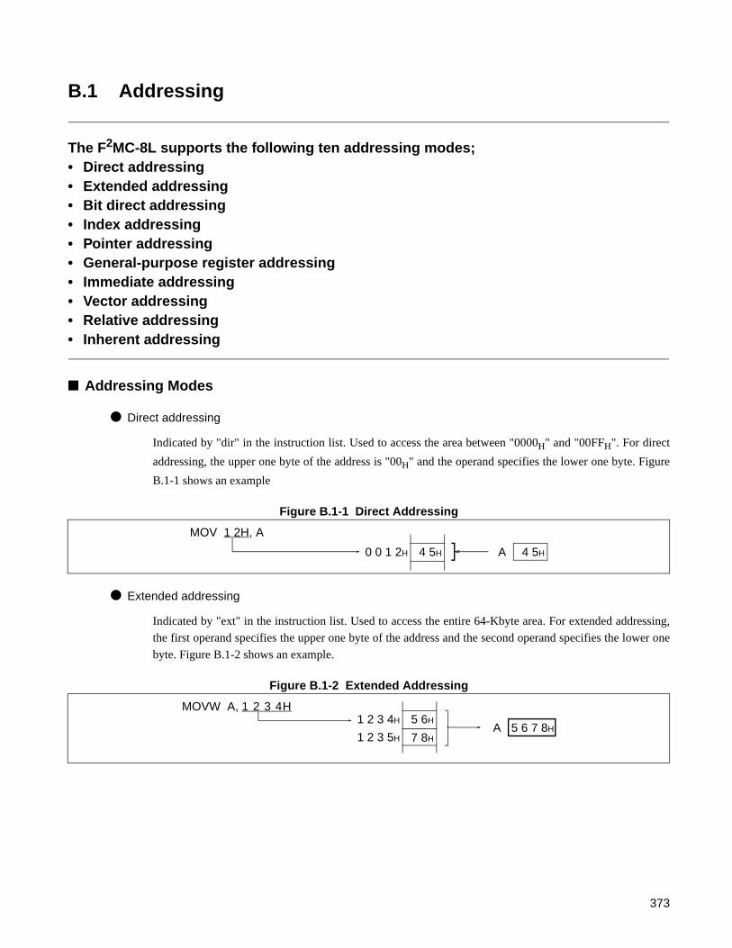
B.1 Addressing
The F2MC-8L supports the following ten addressing modes;• Direct addressing• Extended addressing• Bit direct addressing• Index addressing• Pointer addressing• General-purpose register addressing• Immediate addressing• Vector addressing• Relative addressing• Inherent addressing
Addressing Modes
Direct addressing
Indicated by "dir" in the instruction list. Used to access the area between "0000H" and "00FFH". For direct
addressing, the upper one byte of the address is "00H" and the operand specifies the lower one byte. Figure
B.1-1 shows an example
Figure B.1-1 Direct Addressing
Extended addressing
Indicated by "ext" in the instruction list. Used to access the entire 64-Kbyte area. For extended addressing,
the first operand specifies the upper one byte of the address and the second operand specifies the lower one
byte. Figure B.1-2 shows an example.
Figure B.1-2 Extended Addressing
MOV 1 2H, A
0 0 1 2H 4 5H A 4 5H
5 6H
7 8HA 5 6 7 8H
1 2 3 4H
1 2 3 5H
MOVW A, 1 2 3 4H
373

APPENDIX B Instructions
Bit direct addressing
Indicated by "dir: b" in the instruction list. Used to access the area between "0000H" and "00FFH" in bit
units. For bit direct addressing, the upper one byte of the address is "00H", the operand specifies the lower
one byte of the address, and the lower three bits of the operation code specify the bit position. Figure B.1-3
shows an example.
Figure B.1-3 Bit Direct Addressing
Index addressing
Indicated by "@IX+off" in the instruction list. Used to access the entire 64-Kbyte area. Index addressing
generates the address is obtained by adding the sign-extended contents of the first operand to the index
register (IX). Figure B.1-4 shows an example.
Figure B.1-4 Index Addressing
Pointer addressing
Indicated by "@EP" in the instruction list. Used to access the entire 64-Kbyte area. Pointer addressing uses
the extra pointer (EP) the address. Figure B.1-5 shows an example.
Figure B.1-5 Pointer Addressing
General-purpose register addressing
Indicated by "Ri" in the instruction list. Used to access the general-purpose register area register bank. For
general-purpose register addressing, the upper one byte of the address is fixed at "01" and the lower byte is
generated from the register bank pointer (RP) and the lower three bits of the operation code. The CPU
accesses the resulting address. Figure B.1-6 shows an example.
Figure B.1-6 General-purpose Register Addressing
SETB 3 4H : 20034H XXXXX1XXB
76543210
1 2H
3 4HA 1 2 3 4H
2 7 F FH
2 8 0 0H
MOVW A, @IX+5 AH
IX 2 7 A 5H +
1 2H
3 4HA 1 2 3 4H
2 7 A 5H
2 7 A 6H
MOVW A, @EP
EP 2 7 A 5H
A BH A A BH0 1 5 6H
MOV A, R6
RP 0 1 0 1 0B +
374

Immediate addressing
Indicated by "#d8" in the instruction list. Used when immediate data is required. In immediate addressing,
the operand is used directly as immediate data. The operation code determines whether the data is byte or
word. Figure B.1-7 shows an example.
Figure B.1-7 Immediate Addressing
Vector addressing
Indicated by "vct" in the instruction list. Used to branch to a subroutine address stored in the vector table.
For vector addressing, the "vct" data is contained in the operation code. Table B.1-1 lists the
correspondence between "vct" and the resulting address.
Figure B.1-8 shows an example.
Figure B.1-8 Vector Addressing
MOV A, #5 6H
A 5 6H
Table B.1-1 Vector Table Address Corresponding to "vct"
#vct Vector table address (branch destination upper address: lower address)
0 FFC0H : FFC1H
1 FFC2H : FFC3H
2 FFC4H : FFC5H
3 FFC6H : FFC7H
4 FFC8H : FFC9H
5 FFCAH : FFCBH
6 FFCCH : FFCDH
7 FFCEH : FFCFH
F EH
D CHPC F E D CH
F F C AH
F F C BH
CALLV #5
(Conversion)
375
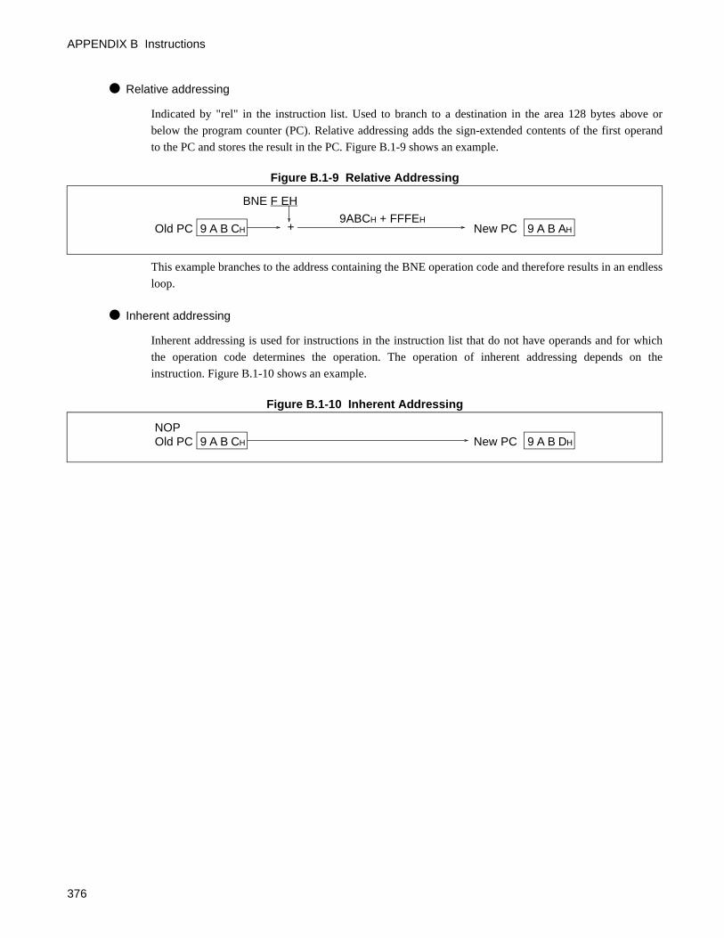
APPENDIX B Instructions
Relative addressing
Indicated by "rel" in the instruction list. Used to branch to a destination in the area 128 bytes above or
below the program counter (PC). Relative addressing adds the sign-extended contents of the first operand
to the PC and stores the result in the PC. Figure B.1-9 shows an example.
Figure B.1-9 Relative Addressing
This example branches to the address containing the BNE operation code and therefore results in an endless
loop.
Inherent addressing
Inherent addressing is used for instructions in the instruction list that do not have operands and for which
the operation code determines the operation. The operation of inherent addressing depends on the
instruction. Figure B.1-10 shows an example.
Figure B.1-10 Inherent Addressing
Old PC
BNE F EH
9ABCH + FFFEHNew PC+9 A B CH 9 A B AH
Old PC New PC9 A B CH 9 A B DH
NOP
376

B.2 Special Instructions
This section describes special instructions, other than addressing.
Special Instructions
JMP @A
This instruction moves the address contained in the accumulator (A) to the program counter (PC) and
branches to the new address. This instruction can be used to perform an N option branch by placing N
branch destination addresses in a table and moving the desired address to the accumulator.
Figure B.2-1 shows an outline of the instruction operation
Figure B.2-1 JMP @A
MOVW A,PC
This instruction stores the PC contents in the accumulator A. This performs the opposite operation to "JMP
@A". By executing this instruction in the main routine and calling a particular subroutine, the subroutine
can determine whether the contents of A match a predetermined value. The subroutine can check whether
program runaway has occurred by checking whether or not execution has branched from an expected
location.
Figure B.2-2 shows an outline of the instruction operation
Figure B.2-2 MOVW A,PC
The content of A after executing this instruction is the address of the next instruction (not the address
containing the operation code of this instruction. Accordingly, the value "1234H" stored in A in the
example shown in Figure B.2-2 is the address of the next operation code after "MOVW A, PC".
(Before execution) (After execution)
A 1 2 3 4H
Old PC X X X XH
A 1 2 3 4H
New PC 1 2 3 4H
(Before execution) (After execution)
A X X X XH
Old PC 1 2 3 3H
A 1 2 3 4H
New PC 1 2 3 4H
377
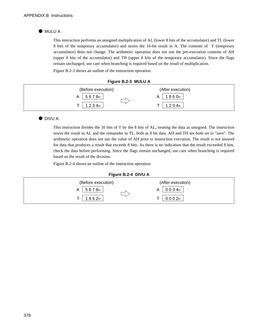
APPENDIX B Instructions
MULU A
This instruction performs an unsigned multiplication of AL (lower 8 bits of the accumulator) and TL (lower
8 bits of the temporary accumulator) and stores the 16-bit result in A. The contents of T (temporary
accumulator) does not change. The arithmetic operation does not use the pre-execution contents of AH
(upper 8 bits of the accumulator) and TH (upper 8 bits of the temporary accumulator). Since the flags
remain unchanged, use care when branching is required based on the result of multiplication.
Figure B.2-3 shows an outline of the instruction operation.
Figure B.2-3 MULU A
DIVU A
This instruction divides the 16 bits of T by the 8 bits of AL, treating the data as unsigned. The instruction
stores the result in AL and the remainder in TL, both as 8 bit data. AH and TH are both set to "zero". The
arithmetic operation does not use the value of AH prior to instruction execution. The result is not assured
for data that produces a result that exceeds 8 bits. As there is no indication that the result exceeded 8 bits,
check the data before performing. Since the flags remain unchanged, use care when branching is required
based on the result of the division.
Figure B.2-4 shows an outline of the instruction operation
Figure B.2-4 DIVU A
(Before execution) (After execution)
A 5 6 7 8H
T 1 2 3 4H
A 1 8 6 0H
T 1 2 3 4H
(Before execution) (After execution)
A 5 6 7 8H
T 1 8 6 2H
A 0 0 3 4H
T 0 0 0 2H
378
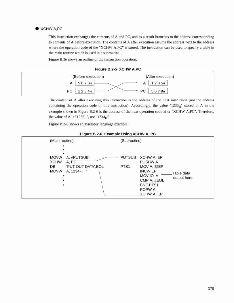
XCHW A,PC
This instruction exchanges the contents of A and PC, and as a result branches to the address corresponding
to contents of A before execution. The contents of A after execution assume the address next to the address
where the operation code of the “XCHW A,PC” is stored. The instruction can be used to specify a table in
the main routine which is used in a subroutine.
Figure B.2e shows an outline of the instruction operation.
Figure B.2-5 XCHW A,PC
The content of A after executing this instruction is the address of the next instruction (not the address
containing the operation code of this instruction). Accordingly, the value "1235H" stored in A in the
example shown in Figure B.2-6 is the address of the next operation code after "XCHW A,PC". Therefore,
the value of A is "1235H", not "1234H".
Figure B.2-6 shows an assembly language example.
Figure B.2-6 Example Using XCHW A, PC
(Before execution) (After execution)
A 5 6 7 8H
PC 1 2 3 4H
A 1 2 3 5H
PC 5 6 7 8H
(Main routine) (Subroutine)•••
MOVW A, #PUTSUB PUTSUB XCHW A, EPXCHW A, PC PUSHW ADB ‘PUT OUT DATA’,EOL PTS1 MOV A, @EPMOVW A, 1234H INCW EP
• MOV IO, A• CMP A, #EOL• BNE PTS1
POPW AXCHW A, EP
Table data output here.
379
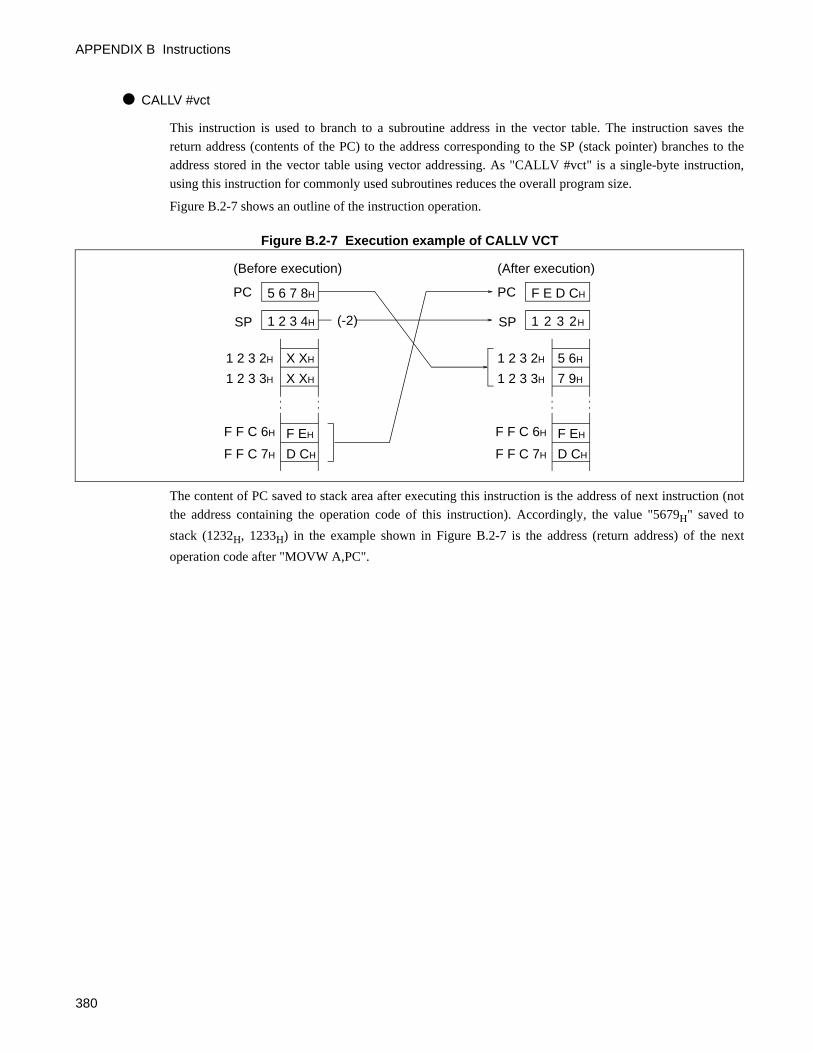
APPENDIX B Instructions
CALLV #vct
This instruction is used to branch to a subroutine address in the vector table. The instruction saves the
return address (contents of the PC) to the address corresponding to the SP (stack pointer) branches to the
address stored in the vector table using vector addressing. As "CALLV #vct" is a single-byte instruction,
using this instruction for commonly used subroutines reduces the overall program size.
Figure B.2-7 shows an outline of the instruction operation.
Figure B.2-7 Execution example of CALLV VCT
The content of PC saved to stack area after executing this instruction is the address of next instruction (not
the address containing the operation code of this instruction). Accordingly, the value "5679H" saved to
stack (1232H, 1233H) in the example shown in Figure B.2-7 is the address (return address) of the next
operation code after "MOVW A,PC".
(Before execution) (After execution)
PC
SP
5 6 7 8H
1 2 3 4H
PC
SP
F E D CH
1 2 3 2H
X XH
X XH
F EH
D CH
1 2 3 2H
1 2 3 3H
F F C 6H
F F C 7H
5 6H
7 9H
F EH
D CH
1 2 3 2H
1 2 3 3H
F F C 6H
F F C 7H
(-2)
380
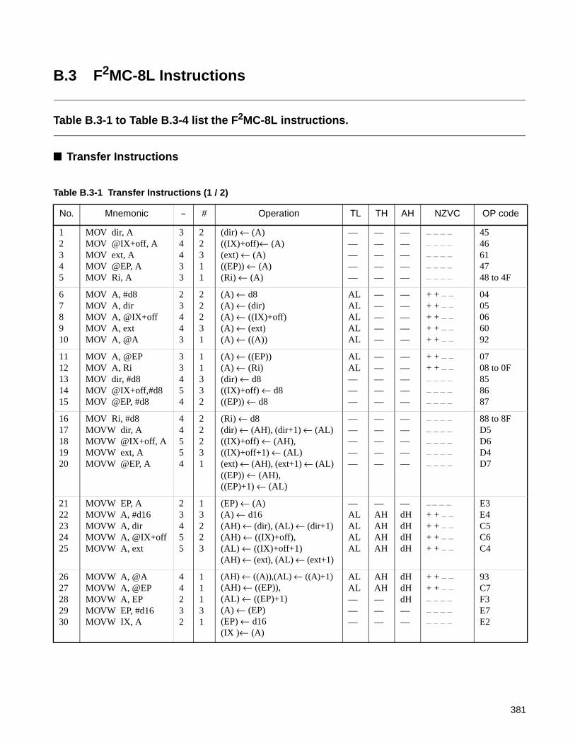
B.3 F2MC-8L Instructions
Table B.3-1 to Table B.3-4 list the F2MC-8L instructions.
Transfer Instructions
Table B.3-1 Transfer Instructions (1 / 2)
No. Mnemonic ~ # Operation TL TH AH NZVC OP code
12345
MOV dir, AMOV @IX+off, AMOV ext, AMOV @EP, AMOV Ri, A
34433
22311
(dir) ← (A)((IX)+off)← (A)(ext) ← (A)((EP)) ← (A)(Ri) ← (A)
—————
—————
—————
— — — —
— — — —
— — — —
— — — —
— — — —
4546614748 to 4F
678910
MOV A, #d8MOV A, dirMOV A, @IX+offMOV A, extMOV A, @A
23443
22231
(A) ← d8(A) ← (dir)(A) ← ((IX)+off)(A) ← (ext)(A) ← ((A))
ALALALALAL
—————
—————
+ + — —
+ + — —
+ + — —
+ + — —
+ + — —
0405066092
1112131415
MOV A, @EPMOV A, RiMOV dir, #d8MOV @IX+off,#d8MOV @EP, #d8
33454
11332
(A) ← ((EP))(A) ← (Ri)(dir) ← d8((IX)+off) ← d8((EP)) ← d8
ALAL———
—————
—————
+ + — —
+ + — —
— — — —
— — — —
— — — —
0708 to 0F858687
1617181920
MOV Ri, #d8MOVW dir, AMOVW @IX+off, AMOVW ext, AMOVW @EP, A
44554
22231
(Ri) ← d8(dir) ← (AH), (dir+1) ← (AL)((IX)+off) ← (AH), ((IX)+off+1) ← (AL)(ext) ← (AH), (ext+1) ← (AL)((EP)) ← (AH),((EP)+1) ← (AL)
—————
—————
—————
— — — —
— — — —
— — — —
— — — —
— — — —
88 to 8FD5D6D4D7
2122232425
MOVW EP, AMOVW A, #d16MOVW A, dirMOVW A, @IX+offMOVW A, ext
23455
13223
(EP) ← (A)(A) ← d16(AH) ← (dir), (AL) ← (dir+1)(AH) ← ((IX)+off),(AL) ← ((IX)+off+1)(AH) ← (ext), (AL) ← (ext+1)
—ALALALAL
—AHAHAHAH
—dHdHdHdH
— — — —
+ + — —
+ + — —
+ + — —
+ + — —
E3E4C5C6C4
2627282930
MOVW A, @AMOVW A, @EPMOVW A, EPMOVW EP, #d16MOVW IX, A
44232
11131
(AH) ← ((A)),(AL) ← ((A)+1)(AH) ← ((EP)),(AL) ← ((EP)+1)(A) ← (EP)(EP) ← d16(IX )← (A)
ALAL———
AHAH———
dHdHdH——
+ + — —
+ + — —
— — — —
— — — —
— — — —
93C7F3E7E2
381

APPENDIX B Instructions
Notes:
• The automatic transfer to the T register is TL←AL for instructions that perform a byte transfer toA.
• Operands in more than one operand instruction must be stored in the order in which theirmnemonics are written.
3132333435
MOVW A, IXMOVW SP, AMOVW A, SPMOV @A, TMOVW @A, T
22234
11111
(A) ← (IX)(SP) ← (A)(A) ← (SP)((A)) ← (T)((A)) ← (TH), ((A)+1) ← (TL)
—————
—————
dH—dH——
— — — —
— — — —
— — — —
— — — —
— — — —
F2E1F18283
3637383940
MOVW IX, #d16MOVW A, PSMOVW PS, AMOVW SP, #d16SWAP
32232
31131
(IX) ← d16(A) ← (PS)(PS) ← (A)(SP) ← d16(AH) ← → (AL)
—————
—————
—dH——AL
— — — —
— — — —
+ + + + — — — —
— — — —
E67071E510
4142434445
SETB dir:bCLRB dir:bXCH A, TXCHW A, TXCHW A, EP
44233
22111
(dir):b ← 1(dir):b ← 0(AL) ← → (TL)(A) ← → (T)(A) ← → (EP)
——ALAL—
———AH—
———dHdH
— — — —
— — — —
— — — —
— — — —
— — — —
A8 to AFA0 to A74243F7
464748
XCHW A, IXXCHW A, SPMOVW A, PC
332
111
(A) ← → (IX)(A )← → (SP)(A) ← (PC)
———
———
dHdHdH
— — — —
— — — —
— — — —
F6F5F0
Table B.3-1 Transfer Instructions (2 / 2)
No. Mnemonic ~ # Operation TL TH AH NZVC OP code
382

Arithmetic Operation Instructions
Table B.3-2 Arithmetic Operation Instructions (1 / 2)
No. Mnemonic ~ # Operation TL TH AH NZVC OP code
12345
ADDC A, RiADDC A, #d8ADDC A, dirADDC A, @IX+offADDC A, @EP
32343
12221
(A) ← (A)+(Ri)+C(A) ← (A)+d8+C(A) ← (A)+(dir)+C(A) ← (A)+((IX)+off)+C(A) ← (A)+((EP))+C
—————
—————
—————
+ + + ++ + + ++ + + ++ + + ++ + + +
28 to 2F24252627
678910
ADDCW AADDC ASUBC A, RiSUBC A, #d8SUBC A, dir
32323
11122
(A) ← (A)+(T)+C(AL) ← (AL)+(TL)+C(A) ← (A)-(Ri)-C(A) ← (A)-d8-C(A) ← (A)-(dir)-C
—————
—————
dH————
+ + + ++ + + ++ + + ++ + + ++ + + +
232238 to 3F3435
1112131415
SUBC A, @IX+offSUBC A, @EPSUBCW ASUBC AINC Ri
43324
21111
(A) ← (A)-((IX)+off)-C(A) ← (A)-((EP))-C(A) ← (T)-(A)-C(AL) ← (TL)-(AL)-C(Ri) ← (Ri)+1
—————
—————
——dH——
+ + + ++ + + ++ + + ++ + + ++ + + —
36373332C8 to CF
1617181920
INCW EPINCW IXINCW ADEC RiDECW EP
33343
11111
(EP) ← (EP)+1(IX) ← (IX)+1(A) ← (A)+1(Ri) ← (Ri)-1(EP) ← (EP)-1
—————
—————
——dH——
— — — —
— — — —
+ + — —
+ + + —
— — — —
C3C2C0D8 to DFD3
2122232425
DECW IXDECW AMULU ADIVU AANDW A
3319213
11111
(IX) ← (IX)-1(A) ← (A)-1(A) ← (AL)*(TL)(A) ← (T)/(AL), MOD → (T)(A) ← (A) ∧ (T)
———dL—
———00—
—dHdH00dH
— — — —
+ + — —
— — — —
— — — —
+ + R —
D2D0011163
2627282930
ORW AXORW ACMP ACMPW ARORC A
33232
11111
(A) ← (A) ∨ (T)(A) ← (A) ∀ (T)
(TL)-(AL)(T)-(A)
—————
—————
dHdH———
+ + R —
+ + R —
+ + + ++ + + ++ + — +
7353121303
31
32333435
ROLC A
CMP A, #d8CMP A, dirCMP A, @EPCMP A, @IX+off
2
2334
1
2212
(A)-d8(A)-(dir)(A)-((EP))(A)-((IX)+off)
—
————
—
————
—
————
+ + — +
+ + + ++ + + ++ + + ++ + + +
02
14151716
3637383940
CMP A, RiDAADASXOR AXOR A, #d8
32222
11112
(A)-(Ri)decimal adjust for additiondecimal adjust for subtraction(A) ← (AL) ∀ (TL)(A) ← (AL) ∀ d8
—————
—————
—————
+ + + ++ + + ++ + + ++ + R —
+ + R —
18 to 1F84945254
→ C → A
C ← A←
383
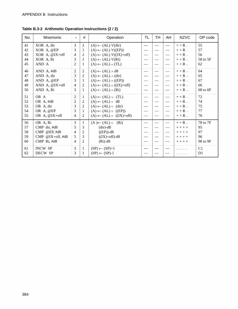
APPENDIX B Instructions
4142434445
XOR A, dirXOR A, @EPXOR A, @IX+offXOR A, RiAND A
33432
21211
(A) ← (AL) ∀ (dir)(A) ← (AL) ∀ ((EP))(A) ← (AL) ∀ ((IX)+off)(A) ← (AL) ∀ (Ri)(A) ← (AL) ∧ (TL)
—————
—————
—————
+ + R —
+ + R —
+ + R —
+ + R —
+ + R —
55575658 to 5F62
4647484950
AND A, #d8AND A, dirAND A, @EPAND A, @IX+offAND A, Ri
23343
22121
(A) ← (AL) ∧ d8(A) ← (AL) ∧ (dir)(A) ← (AL) ∧ ((EP))(A) ← (AL) ∧ ((IX)+off)(A) ← (AL) ∧ (Ri)
—————
—————
—————
+ + R —
+ + R —
+ + R —
+ + R —
+ + R —
6465676668 to 6F
5152535455
OR AOR A, #d8OR A, dirOR A, @EPOR A, @IX+off
22334
12212
(A) ← (AL) ∨ (TL)(A) ← (AL) ∨ d8(A) ← (AL) ∨ (dir)(A) ← (AL) ∨ ((EP))(A) ← (AL) ∨ ((IX)+off)
—————
—————
—————
+ + R —
+ + R —
+ + R —
+ + R —
+ + R —
7274757776
5657585960
OR A, RiCMP dir, #d8CMP @EP, #d8CMP @IX+off, #d8CMP Ri, #d8
35454
13232
(A )← (AL) ∨ (Ri)(dir)-d8((EP))-d8((IX)+off)-d8(Ri)-d8
—————
—————
—————
+ + R —
+ + + ++ + + ++ + + ++ + + +
78 to 7F95979698 to 9F
6162
INCW SPDECW SP
33
11
(SP) ← (SP)+1(SP) ← (SP)-1
——
——
——
— — — —
— — — —
C1D1
Table B.3-2 Arithmetic Operation Instructions (2 / 2)
No. Mnemonic ~ # Operation TL TH AH NZVC OP code
384

Branch Instructions
Other Instructions
Table B.3-3 Branch Instructions
No.
Mnemonic ~ # Operation TL TH AH NZVC OP code
12345
BZ/BEQ relBNZ/BNE relBC/BLO relBNC/BHS relBN rel
33333
22222
if Z=1 then PC ← PC+relif Z=0 then PC ← PC+relif C=1 then PC ← PC+relif C=0 then PC ← PC+relif N=1 then PC ← PC+rel
—————
—————
—————
— — — —
— — — —
— — — —
— — — —
— — — —
FDFCF9F8FB
678910
BP relBLT relBGE relBBC dir:b, relBBS dir:b, rel
33355
22233
if N=0 then PC ← PC+relif V ∀ N=1 then PC ← PC+relif V ∀ N=0 then PC ← PC+relif (dir:b)=0 then PC ← PC+relif (dir:b)=1 then PC ← PC+rel
—————
—————
—————
— — — —
— — — —
— — — —
— + — —
— + — —
FAFFFEB0 to B7B8 to BF
1112131415
JMP @AJMP extCALLV #vctCALL extXCHW A, PC
23663
13131
(PC) ← (A)(PC) ← extvector callsubroutine call(PC) ← (A), (A) ← (PC)+1
—————
—————
————dH
— — — —
— — — —
— — — —
— — — —
— — — —
E021E8 to EF31F4
1617
RETRETI
46
11
return from subroutinereturn form interrupt
–—
——
——
— — — —
restore2030
Table B.3-4 Other Instructions
No.
Mnemonic ~ # Operation TL TH AH NZVC OP code
12345
PUSHW APOPW APUSHW IXPOPW IXNOP
44441
11111
((SP))<-(A),(SP)<-(SP)-2(A)<-((SP)),(SP)<-(SP)+2((SP))<-(IX),(SP)<-(SP)-2(IX)<-((SP)),(SP)<-(SP)+2No operation
————–
—————
—dH———
— — — —
— — — —
— — — —
— — — —
— — — —
4050415100
6789
CLRCSETCCLRISETI
1111
1111
(C)<-0(C)<-1(I)<-0(I)<-1
————
————
————
— — — R— — — S— — — —
— — — —
81918090
385
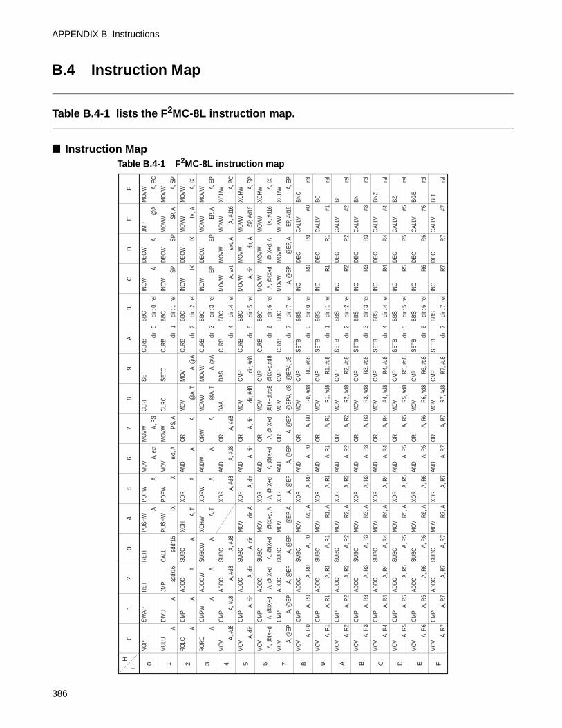
APPENDIX B Instructions
B.4 Instruction Map
Table B.4-1 lists the F2MC-8L instruction map.
Instruction MapTable B.4-1 F2MC-8L instruction map
0 1 2 3 4 5 6 7 8 9 A B C D E F
NO
P
MU
LU
A
ROLC
A
ROR
C
A
MO
V
A, #
d8
MO
V
A,
dir
MO
V
A, @
IX+d
MO
V
A, @
EP
MO
V
A
, R0
MO
V
A
, R1
MO
V
A
, R2
MO
V
A
, R3
MO
V
A
, R4
MO
V
A
, R5
MO
V
A
, R6
MO
V
A
, R7
SWAP
DIV
U
A
CM
P
A
CM
PW
A
CM
P
A, #
d8
CM
P
A
, dir
CM
P
A, @
IX+d
CM
P
A, @
EP
CM
P
A
, R0
CM
P
A
, R1
CM
P
A
, R2
CM
P
A
, R3
CM
P
A
, R4
CM
P
A
, R5
CM
P
A
, R6
CM
P
A
, R7
RET
JMP
add
r16
ADD
C
A
ADD
CW
A
ADD
C
A, #
d8
ADD
C
A
, dir
ADD
C
A, @
IX+d
ADD
C
A, @
EP
ADD
C
A
, R0
ADD
C
A
, R1
ADD
C
A
, R2
ADD
C
A
, R3
ADD
C
A
, R4
ADD
C
A
, R5
ADD
C
A
, R6
ADD
C
A
, R7
RET
I
CAL
L
add
r16
SUBC
A
SUBC
W
A
SUBC
A, #
d8
SUBC
A,
dir
SUBC
A, @
IX+d
SUBC
A, @
EP
SUBC
A
, R0
SUBC
A
, R1
SUBC
A
, R2
SUBC
A
, R3
SUBC
A
, R4
SUBC
A
, R5
SUBC
A
, R6
SUBC
A
, R7
PUSH
W
A
PUSH
W
IX
XCH
A
, T
XCH
W
A
, T
MO
V
d
ir, A
MO
V
@IX
+d, A
MO
V
@EP
, A
MO
V
R
0, A
MO
V
R
1, A
MO
V
R
2, A
MO
V
R
3, A
MO
V
R
4, A
MO
V
R
5, A
MO
V
R
6, A
MO
V
R
7, A
POPW
A
POPW
IX
XOR
A
XORW
A
XOR
A, #
d8
XOR
A
, dir
XOR
A, @
IX+d
XOR
A, @
EP
XOR
A
, R0
XOR
A
, R1
XOR
A
, R2
XOR
A
, R3
XOR
A
, R4
XOR
A
, R5
XOR
A
, R6
XOR
A
, R7
MO
V
A,
ext
MO
V
ex
t, A
AND
A
ANDW
A
AND
A, #
d8
AND
A
, dir
AND
A, @
IX+d
AND
A, @
EP
AND
A
, R0
AND
A
, R1
AND
A
, R2
AND
A
, R3
AND
A
, R4
AND
A
, R5
AND
A
, R6
AND
A
, R7
MO
VW
A,
PS
MO
VW
PS
, A
OR
A
ORW
A
OR
A, #
d8
OR
A,
dir
OR
A, @
IX+d
OR
A, @
EP
OR
A
, R0
OR
A
, R1
OR
A
, R2
OR
A
, R3
OR
A
, R4
OR
A
, R5
OR
A
, R6
OR
A
, R7
CLR
I
CLR
C
MO
V
@A,
T
MO
VW
@A,
T
DAA
MO
V
dir,
#d8
MO
V
@IX
+d,#
d8
MO
V
@EP
#, d
8
MO
V
R0,
#d8
MO
V
R1,
#d8
MO
V
R2,
#d8
MO
V
R3,
#d8
MO
V
R4,
#d8
MO
V
R5,
#d8
MO
V
R6,
#d8
MO
V
R7,
#d8
SETI
SETC
MO
V
A, @
A
MO
VW
A, @
A
DAS
CM
P
dir,
#d8
CM
P
@IX
+d,#
d8
CM
P
@EP
#, d
8
CM
P
R
0, #
d8
CM
P
R
1, #
d8
CM
P
R
2, #
d8
CM
P
R
3, #
d8
CM
P
R
4, #
d8
CM
P
R
5, #
d8
CM
P
R
6, #
d8
CM
P
R
7, #
d8
CLR
B
d
ir : 0
CLR
B
d
ir : 1
CLR
B
d
ir : 2
CLR
B
d
ir : 3
CLR
B
d
ir : 4
CLR
B
d
ir : 5
CLR
B
d
ir : 6
CLR
B
d
ir : 7
SETB
d
ir : 0
SETB
d
ir : 1
SETB
d
ir : 2
SETB
d
ir : 3
SETB
d
ir : 4
SETB
d
ir : 5
SETB
d
ir : 6
SETB
d
ir : 7
BBC
di
r : 0
, rel
BBC
di
r : 1
, rel
BBC
di
r : 2
, rel
BBC
di
r : 3
, rel
BBC
di
r : 4
, rel
BBC
di
r : 5
, rel
BBC
di
r : 6
, rel
BBC
di
r : 7
, rel
BBS
di
r : 0
, rel
BBS
di
r : 1
, rel
BBS
di
r : 2
, rel
BBS
di
r : 3
, rel
BBS
di
r : 4
, rel
BBS
di
r : 5
, rel
BBS
di
r : 6
, rel
BBS
di
r : 7
, rel
INC
W
A
INC
W
SP
INC
W
IX
INC
W
EP
MO
VW
A,
ext
MO
VW
A,
dir
MO
VW
A, @
IX+d
MO
VW
A
, @EP
INC
R0
INC
R1
INC
R2
INC
R3
INC
R4
INC
R5
INC
R6
INC
R7
DEC
W
A
DEC
W
SP
DEC
W
IX
DEC
W
EP
MO
VW
ex
t, A
MO
VW
d
ir, A
MO
VW
@IX
+d, A
MO
VW
@EP
, A
DEC
R
0
DEC
R
1
DEC
R
2
DEC
R
3
DEC
R
4
DEC
R
5
DEC
R
6
DEC
R
7
JMP
@A
MO
VW
SP
, A
MO
VW
IX
, A
MO
VW
EP
, A
MO
VW
A, #
d16
MO
VW
S
P, #
d16
MO
VW
I
X, #
d16
MO
VW
E
P, #
d16
CAL
LV
#0
CAL
LV
#1
CAL
LV
#2
CAL
LV
#3
CAL
LV
#4
CAL
LV
#5
CAL
LV
#6
CAL
LV
#7
MO
VW
A,
PC
MO
VW
A,
SP
MO
VW
A,
IX
MO
VW
A,
EP
XCH
W
A,
PC
XCH
W
A,
SP
XCH
W
A,
IX
XCH
W
A,
EP
BNC
rel
BC
rel
BP
rel
BN
rel
BNZ
rel
BZ
rel
BGE
rel
BLT
rel
01
23
45
67
89
AB
CD
EF
LH
386

B.5 Bit Manipulation Instructions (SETB, CLRB)
The bit manipulation instructions use a different read operation to the normal operation for some bits of peripheral function registers.
Read-modify-write OperationBit manipulation instructions set to "1" (SETB) or clear to "0" (CLRB) the specified bit only of a register or
RAM location. However, as the CPU handles data in 8-bit units, the actual operation consists of reading the
8-bit data, modifying the specified bit, then writing the result back to the same address. This is called a
read-modify-write operation.
Table B.5-1 shows the bus operation for bit manipulation instructions
Read Source when Executing Bit Manipulation InstructionsThe read source for a read-modify-write of some I/O ports and interrupt request flag bits is different than
for a standard read.
I/O ports (Bit manipulation instructions)
For some I/O ports, a standard read reads the I/O pin values whereas a bit manipulation instruction reads,
the output latch value. This is to prevent unintentionally modifying other output latch bit values and is
independent of the pin input/output direction or pin state.
Interrupt request flag bits (Bit manipulation instructions)
For interrupt request flag bits, a standard read reads the flag bit to determine whether an interrupt has
occurred. Bit manipulation instructions, however, always read interrupt request flag bits as "1". This is to
prevent unintentionally clearing the flag by writing "0" to the interrupt request flag bit when performing bit
manipulation of a different bit.
Table B.5-1 Bus Operation for Bit Manipulation Instructions
Code Mnemonic ~ Cycle Address bus Data bus RD WR RMW
A0 to A7A8 to AF
CLRB dir:b
SETB dir:b
4 1234
N+1dir addressdir addressN+2
dirDataDataNext instruction
0010
1101
0100
387
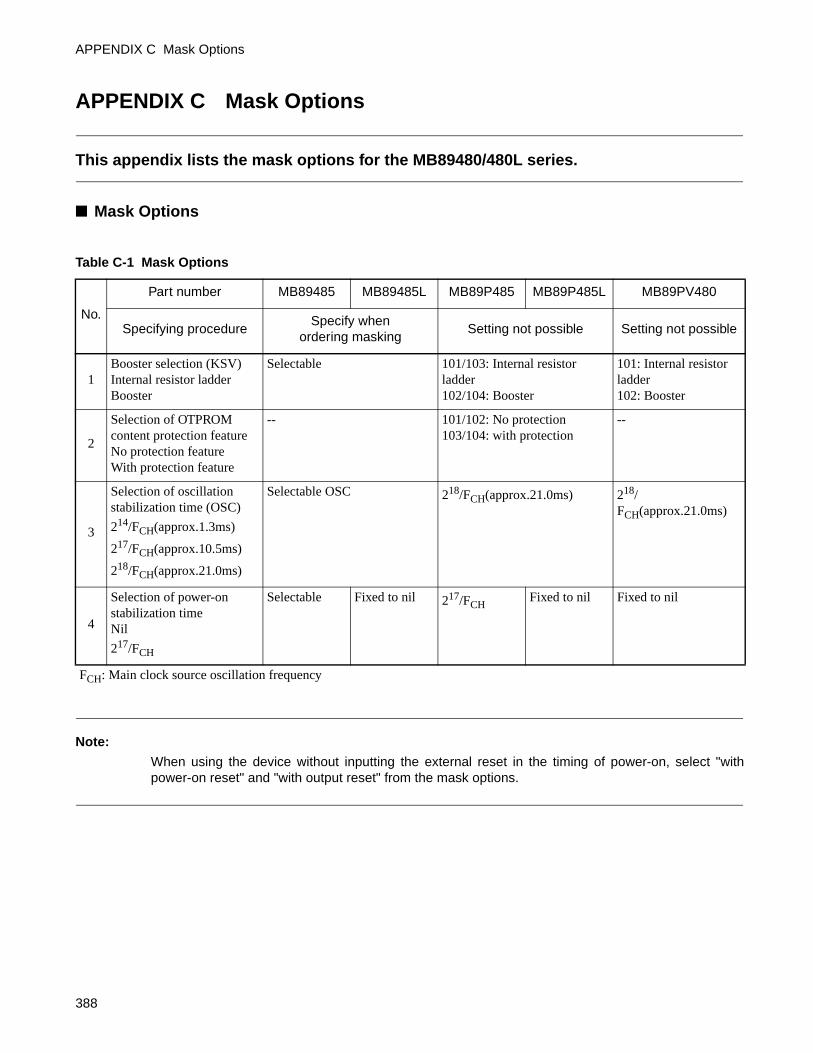
APPENDIX C Mask Options
APPENDIX C Mask Options
This appendix lists the mask options for the MB89480/480L series.
Mask Options
Note:
When using the device without inputting the external reset in the timing of power-on, select "withpower-on reset" and "with output reset" from the mask options.
Table C-1 Mask Options
No.
Part number MB89485 MB89485L MB89P485 MB89P485L MB89PV480
Specifying procedureSpecify when
ordering maskingSetting not possible Setting not possible
1Booster selection (KSV)Internal resistor ladderBooster
Selectable 101/103: Internal resistor ladder102/104: Booster
101: Internal resistor ladder102: Booster
2
Selection of OTPROM content protection featureNo protection featureWith protection feature
-- 101/102: No protection103/104: with protection
--
3
Selection of oscillation stabilization time (OSC)
214/FCH(approx.1.3ms)
217/FCH(approx.10.5ms)
218/FCH(approx.21.0ms)
Selectable OSC 218/FCH(approx.21.0ms) 218/FCH(approx.21.0ms)
4
Selection of power-on stabilization timeNil
217/FCH
Selectable Fixed to nil 217/FCHFixed to nil Fixed to nil
FCH: Main clock source oscillation frequency
388

APPENDIX D Programming Specifications for one-time PROM and EPROM Microcontrollers
In MB89P485/L, there is a built-in PROM which can be programmed with Serial programmer by using dedicated adapter. Optionally, it can also be programmed with a parallel programmer and dedicated adapter.
One-time PROM productThere are two one-time PROM products, MB89P485/L in this series.
There is a built-in PROM in MB89P485/L. The built-in PROM can be programmed with serial programmer
and parallel programmer with dedicated adaptor. Please refer section "D.1 Programming One-time PROM
Microcontroller with serial programmer" and "D.2 Programming One-time PROM Microcontroller parallel
programmer" for detail.
The following show the one-time PROM product with different option.
Piggyback/Evaluation DeviceThere is a piggyback/evaluation product MB89PV480 in this series.
There is no built-in PROM in MB89PV480.
The EPROM used by MB89PV480 can be programmed with an general-purpose EPROM programmer with
dedicated adaptor. Please refer "D.3 Programming EPROM for Piggyback/Evaluation Device" for detail.
Table D-1 One-Time PROM programming option
PackageProgrammable with Serial
ProgrammerProgrammable with parallel
Programmer
MB89P485/P485L-101 Yes Yes
MB89P485/P485L-102 Yes Yes
MB89P485/P485L-103* Yes No
MB89P485/P485L-104* Yes No
* : OTPROM content protection feature is available.
389

APPENDIX D Programming Specifications for one-time PROM and EPROM Microcontrollers
D.1 Programming One-time PROM Microcontroller with serial programmer
This section describes programming One-time PROM microcontroller with FUJITSU FLASH programmer.
Programming the OTPROM To program the OTPROM use FUJITSU MCU programmer MB91919-001.
Inquiry : Fujitsu Microelectronics Asia Pte Ltd. : TEL (65)-6628-1-0770
FAX (65)-6628-1-0220
Programming Adaptor for OTPROMTo program the OTPROM using FUJITSU MCU programmer MB91919-001, use the programming
adapter listed below.
Inquiry : Fujitsu Microelectronics Asia Pte Ltd. : TEL (65)-6628-1-0770
FAX (65)-6628-1-0220
OTPROM Content ProtectionFor product with OTPROM content protection feature (MB89P485-103, MB89P485-104), OTPROM
content can be read using serial programmer if the OTPROM content protection mechanism is not
activated.
One predefined area of the OTPROM (FFFCH) is assigned to be used for preventing the read access of
OTPROM content. If the protection code "00H" is written in this address (FFFCH), the OTPROM content
cannot be read by any serial programmer.
Note:
The program written into the OTPROM cannot be verified once the OTPROM protection code iswritten ("00H" in FFFCH). It is advised to write the OTPROM protection code at last.
Programming YieldAll bits cannot be programmed at Fujitsu Shipping test to a blanked OTPROM microcontroller, due to its
nature. For this reason, a programming yield of 100% cannot be assured at all times.
Package Compatible socker adaptor
DIP-64P-M01 MB91919-812
FPT-64P-M09 MB91919-813
390

D.2 Programming One-time PROM Microcontroller parallel programmer
This section describes programming One-time PROM microcontroller with parallel programmer.
OTP Programming Adaptor and Recommended ROM Write
Inquiry : Fujitsu Microelectronics Asia Pte Ltd. : TEL (65)-6628-1-0770
Minato electronics Co., Ltd. : TEL (81)-45-59-1-5611
Writing Data to the OTPROM Using Writer from Minato Electronics Co., Ltd.1. Set the OTPROM writer for the CU50-OTP (device code: T.B.D.).
2. Load the program data to the OTPROM writer.
3. Write data using the OTPROM writer.
Programming YieldAll bits cannot be programmed at Fujitsu shipping test to a blanked OTPROM microcomputer, due to its
nature. For this reason, a programming yield of 100% cannot be assured at all times.
OTPROM Content ProtectionThis feature is available in MB89P485/P485L-103 and MB89P485/P485L-104 only. It is not available in
product which can be programmed by parallel programmer, i.e. MB89P485/P485L-101 and MB89P485/
P485L-102
Package name
Applicable adapter model Recommended writer maker and writer
Fujitsu Microelectronics Asia Pte Ltd.
Minato electronics Co., Ltd. Fujitsu MCU Programmer
MODEL 1890A MB91919 - 001
DIP-64P-M01 MB91919-604 Under evaluation Available
FPT-64P-M09 MB91919-605 Under evaluation Available
391

APPENDIX D Programming Specifications for one-time PROM and EPROM Microcontrollers
D.3 Programming EPROM for Piggyback/Evaluation Device
This section describes programming EPROM for piggyback/evaluation device.
EPROM for UseMBM27C256A-20TVM
Programming Socket AdaptorTo program to the PROM using an EPROM programmer, use the socket adaptor (manufacturer:Sun Hayato Co., Ltd.) listed below.
Inquiry: Sun Hayato Co., Ltd.: TEL 81-3-3986-0403
Memory Space
Figure D.3-1 Memory Map of Piggyback/Evaluation Device
Programming to EPROM1. Set the EPROM programmer to the MBM27C256A.
2. Load program data into the EPROM programmer at 0000H to 7FFFH.
3. Program to 0000H to 7FFFH with the EPROM programmer.
Table D.3-1 Programming Socket Adaptor
Package Adaptor socket part number
LCC-32 (Rectangle) ROM-32LC-28DP-S
Address
Normal operating mode
Corresponding addresses on the EPROM programmer
0000H
7FFFH
0000H
0080H
0480H
8000H
FFFFH
I/O
RAM
Not available
PROM32 Kbytes
EPROM32 Kbytes
392
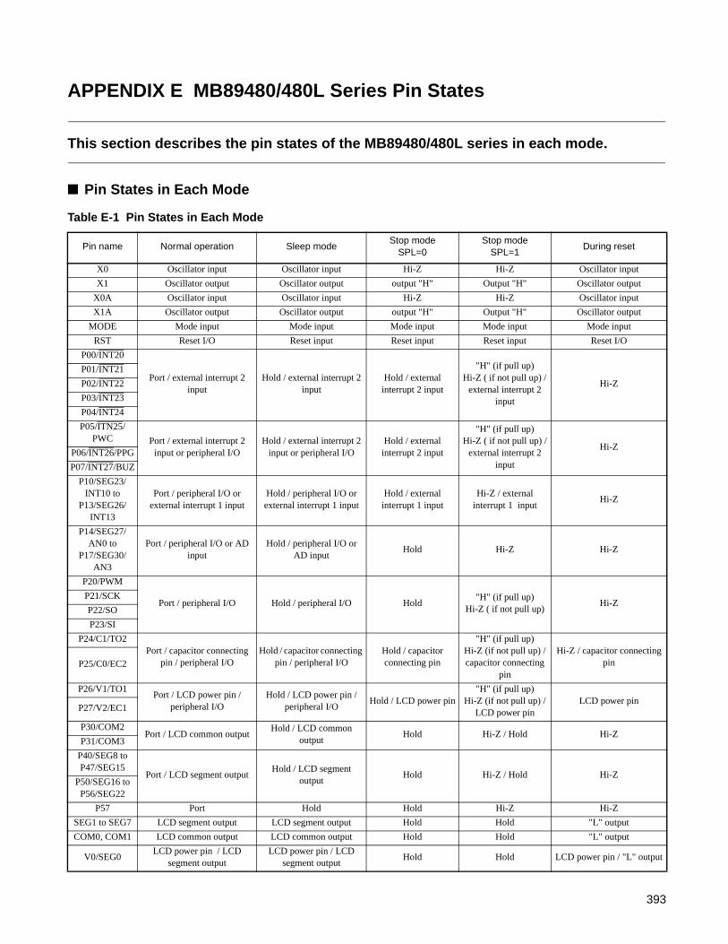
APPENDIX E MB89480/480L Series Pin States
This section describes the pin states of the MB89480/480L series in each mode.
Pin States in Each Mode
Table E-1 Pin States in Each Mode
Pin name Normal operation Sleep modeStop mode
SPL=0Stop mode
SPL=1During reset
X0 Oscillator input Oscillator input Hi-Z Hi-Z Oscillator input
X1 Oscillator output Oscillator output output "H" Output "H" Oscillator output
X0A Oscillator input Oscillator input Hi-Z Hi-Z Oscillator input
X1A Oscillator output Oscillator output output "H" Output "H" Oscillator output
MODE Mode input Mode input Mode input Mode input Mode input
RST Reset I/O Reset input Reset input Reset input Reset I/O
P00/INT20
Port / external interrupt 2 input
Hold / external interrupt 2 input
Hold / external interrupt 2 input
"H" (if pull up)Hi-Z ( if not pull up) /
external interrupt 2 input
Hi-Z
P01/INT21
P02/INT22
P03/INT23
P04/INT24
P05/ITN25/PWC Port / external interrupt 2
input or peripheral I/OHold / external interrupt 2
input or peripheral I/OHold / external
interrupt 2 input
"H" (if pull up)Hi-Z ( if not pull up) /
external interrupt 2 input
Hi-ZP06/INT26/PPG
P07/INT27/BUZ
P10/SEG23/INT10 to
P13/SEG26/INT13
Port / peripheral I/O or external interrupt 1 input
Hold / peripheral I/O or external interrupt 1 input
Hold / external interrupt 1 input
Hi-Z / external interrupt 1 input
Hi-Z
P14/SEG27/AN0 to
P17/SEG30/AN3
Port / peripheral I/O or AD input
Hold / peripheral I/O or AD input
Hold Hi-Z Hi-Z
P20/PWM
Port / peripheral I/O Hold / peripheral I/O Hold"H" (if pull up)
Hi-Z ( if not pull up)Hi-Z
P21/SCK
P22/SO
P23/SI
P24/C1/TO2Port / capacitor connecting
pin / peripheral I/OHold / capacitor connecting
pin / peripheral I/OHold / capacitor connecting pin
"H" (if pull up)Hi-Z (if not pull up) / capacitor connecting
pin
Hi-Z / capacitor connecting pinP25/C0/EC2
P26/V1/TO1Port / LCD power pin /
peripheral I/OHold / LCD power pin /
peripheral I/OHold / LCD power pin
"H" (if pull up)Hi-Z (if not pull up) /
LCD power pinLCD power pin
P27/V2/EC1
P30/COM2Port / LCD common output
Hold / LCD common output
Hold Hi-Z / Hold Hi-ZP31/COM3
P40/SEG8 to P47/SEG15
Port / LCD segment outputHold / LCD segment
outputHold Hi-Z / Hold Hi-Z
P50/SEG16 to P56/SEG22
P57 Port Hold Hold Hi-Z Hi-Z
SEG1 to SEG7 LCD segment output LCD segment output Hold Hold "L" output
COM0, COM1 LCD common output LCD common output Hold Hold "L" output
V0/SEG0LCD power pin / LCD
segment outputLCD power pin / LCD
segment outputHold Hold LCD power pin / "L" output
393

APPENDIX E MB89480/480L Series Pin States
394

INDEX
INDEX
The index follows on the next page.This is listed in alphabetic order.
395
INDEX
Index
Numerics
1/2 Bias, 1/2 Duty Output Waveform....................3556-bit PPG
6-bit PPG Function ...........................................2076-bit PPG Timer Function .................................206Block Diagram of 6-bit PPG Timer ....................209Block Diagram of 6-bit PPG Timer Pin ..............211Notes on Using 6-bit PPG Timer........................217Operation of 6-bit PPG Timer............................215Pin of 6-bit PPG Timer .....................................211Programming Example for 6-bit PPG Timer .......219
6-bit PPG Control Register 1 (PPGC1) ................2136-bit PPG Control Register 2 (PPGC2) ................2148-bit Receiving Operation.....................................3188-bit Transmission Operation ...............................3208/16-bit Timer/Counter
8/16-bit Timer/Counter Interrupt........................237Block Diagram of 8/16-bit Timer/Counter ..........224Interrupt Source of 8/16-bit Timer/Counter .........228Notes on Using 8/16-bit Timer/Counter ..............247Pins of 8/16-bit Timer/Counter ..........................226Registers and Vector Table for 8/16-bit Timer/Counter
(11, 12, 21, 22) Interrupt ......................2388-bit Mode Timer 11/21 Interrupt Operation.........2378-bit PWM Timer
8-bit PWM Timer Interrupt Source ....................163Block Diagram of 8-bit PWM Timer ..................160Block Diagram of 8-bit PWM Timer Pin ............162Pin of 8-bit PWM Timer ...................................162Registers and Vector Tables for 8-bit PWM Timer
Interrupts ............................................168
A
A/DA/D Control Register 1 (ADC1) ........................ 283A/D Control Register 2 (ADC2) ........................ 285A/D Conversion Function ................................. 278A/D Converter Interrupt Source......................... 282A/D Converter Power Supply Voltage ............... 280A/D Data Registers (ADDL and ADDH)............ 287Activating A/D Conversion Function ................. 289Block Diagram of A/D Converter ...................... 279Block Diagram of A/D Converter Pin ................ 281Interrupt for A/D Conversion Function .............. 288Notes on Using A/D Converter.......................... 291Operation of A/D Conversion Function .............. 290Pins of A/D Converter ...................................... 281Program Example for A/D Conversion Function
......................................................... 293Register and Vector Table for A/D Converter Interrupt
......................................................... 288Addressing Modes ............................................... 373Arithmetic Operation
Arithmetic Operation Instructions...................... 383
B
Block DiagramBlock Diagram of 6-bit PPG Timer.................... 209Block Diagram of 6-bit PPG Timer Pin .............. 211Block Diagram of 8/16-bit Timer Counter Pins
......................................................... 227Block diagram of 8/16-bit Timer/Counter........... 224Block Diagram of 8-bit PWM Timer.................. 160Block Diagram of 8-bit PWM Timer Pin ............ 162Block Diagram of A/D Converter ...................... 279Block Diagram of A/D Converter Pin ................ 281Block Diagram of Buzzer Output ...................... 326Block Diagram of Buzzer Output Pin................. 327Block Diagram of Clock Controller ..................... 61Block Diagram of External Interrupt 2 Circuit Pins
......................................................... 269Block Diagram of External Interrupt Circuit 2
......................................................... 267Block Diagram of External Reset Pin................... 53Block Diagram of LCD Controller/Driver .......... 333Block Diagram of MB89480/480L Series............... 8Block Diagram of of Pins of Port 0 ...................... 89Block Diagram of of Pins of Port 1 ...................... 95Block Diagram of of Pins of Port 2 .................... 101Block Diagram of of Pins of Port 3 .................... 109Block Diagram of of Pins of Port 4 .................... 113Block Diagram of of Pins of Port 5 .................... 117
396
INDEX
Block Diagram of Pulse Width Count Timer.......................................................... 180
Block Diagram of Pulse Width Count Timer Pins.......................................................... 182
Block Diagram of the External Interrupt 1 Circuit.......................................................... 255
Block Diagram of the External Interrupt 1 Circuit Pins.......................................................... 256
Block Diagram of Time-base Time .................... 124Block Diagram of UART/SIO ........................... 297Block Diagram of UART/SIO Pin ..................... 300Block Diagram of Watch Prescaler .................... 148Block Diagram of Watchdog Timer ................... 137Block Diagrams of LCD Controller/Driver Pin
.......................................................... 342Branch Instructions .............................................. 385Buzzer
Block Diagram of Buzzer Output....................... 326Block Diagram of Buzzer Output Pin ................. 327Buzzer Output Function.................................... 324Buzzer Output Pin............................................ 327Buzzer Output Register..................................... 327Buzzer Register (BUZR)................................... 328Program Example for Buzzer Output ................. 329
C
Changing to a Standby Mode and Interrupts ......... 81Clock
Block Diagram of Clock Controller ..................... 61Clock Generator................................................. 60Clock Mode Operating States .............................. 65Clock Supply Function ............................. 123, 147Clock Supply Map ............................................. 58Configuration of System Clock Control Register
(SYCC)................................................ 63Main Clock Oscillation Stabilization Wait Time
............................................................ 69Main Clock Oscillation Stabilization Wait Time and
the Reset Source ................................... 50Operation of Clock Supply Function .................. 129Operation of Clock supply Function................... 152Operation of Main Clock Mode ........................... 66Operation of Sub clock Mode.............................. 66Speed-Shift (Main Clock Speed-switching) Function
............................................................ 66Sub clock Oscillation Stabilization Wait Time
............................................................ 70Transmission Operation in Clock Asynchronous
Mode ................................................. 316Configuration of Dedicated Register ..................... 31Configuration of General-purpose Registers ......... 37Configuration of Interrupt Level Setting Registers
(ILR1, ILR2, ILR3, ILR4) .............................. 40Configuration of Register Bank Pointer (RP) ......... 36
Configuration of System Clock Control Register (SYCC) .........................................................63
Continuous Receiving Operations ........................319Continuous Transmission Operations ..................321Counter Function ..................................................223
D
Detecting the Start Bit during Receiving Operation...................................................................315
Devices with Internal Voltage Boosters ................339DIP-64P-M01 Package Dimensions .......................12DIP-64P-M01 Pin Assignment..................................9Display Brightness Adjustment when Internal Divider
Resistors are Used.....................................336Display RAM and Output Pins ..............................351
E
Effect of Reset on RAM Contents...........................55EPROM for Use....................................................392External Dividing Resistors...................................338External Interrupt
Block Diagram of External Interrupt 2 Circuit Pins..........................................................269
Block Diagram of External Interrupt Circuit 2..........................................................267
Block Diagram of the External Interrupt 1 Circuit..........................................................255
Block Diagram of the External Interrupt 1 Circuit Pins..........................................................256
External Interrupt 1 Circuit Interrupt Sources..........................................................257
External Interrupt 2 Circuit Function (Level Detection).................................266
External Interrupt 2 Circuit Interrupt Sources..........................................................270
External Interrupt 2 Control Register (EIE2)..........................................................271
External Interrupt 2 Flag Register (EIF2) ............273External Interrupt Control Register 1 (EIC1)
..........................................................258External Interrupt Control Register 2 (EIC2)
..........................................................260Functions of the External Interrupt Circuit 1
..........................................................254Interrupts for External Interrupt 2 Circuit Operation
..........................................................274Interrupts When the External Interrupt Circuit 1 is
Operating ...........................................262Operation of External Interrupt 2 Circuit.............275Operation of the External Interrupt 1 Circuit
..........................................................263Pins of External Interrupt 1 Circuit .....................256Pins of External Interrupt 2 Circuit .....................268
397

INDEX
Program Example for External Interrupt 2 Circuit..........................................................276
Program Example for the External Interrupt 1 Circuit..........................................................264
Register and Vector Table for External Interrupt 2 Circuit Interrupts ................................274
Register and Vector Table for the External Interrupt 1 Circuit Interrupts ................................262
External ResetBlock Diagram of External Reset Pin ...................53Functions of External Reset Pin ...........................53
F
Features of General-purpose Registers .................38FPT-64P-M09 Package Dimensions ......................13FPT-64P-M09 Pin Assignment...............................10Functions of Dedicated Register ............................31Functions of the External Interrupt Circuit 1 .........254
G
General-purpose Register Areas (Addresses: 0100H to 01FFH) ......................28
I
I/OFunctions of I/O Port ..........................................86I/O map ...........................................................368Pin Functions .....................................................16Program Example for I/O Ports..........................120
Instruction Cycle (tinst)............................................64Instruction List Symbols .......................................371Instruction Map.....................................................386Internal Dividing Resistors....................................335Interrupt Acceptance Control Bit ............................34Interrupt for A/D Conversion Function..................288Interrupt for Pulse Width Measurement Function
...................................................................191Interrupt for the Interval Timer Function...............191Interrupt Processing ...............................................42Interrupt Processing Time ......................................46Interrupt Requests from Peripheral Functions........39Interrupts for External Interrupt 2 Circuit Operation
...................................................................274Interrupts for Interval Timer Function .................. 168Interrupts for Interval Timer Function
(Watch Interrupt) ........................................151Interrupts for Time-base Timer Function ..............128Interrupts When the External Interrupt Circuit 1 is
Operating ..................................................262Interval Timer Function ........................122, 178, 222
Interval Timer Function (Square Wave Output Function) ................ 158
Interval Timer Function (Watch Interrupt) ............ 146
L
LCD Control Register 1 (LCR1) ........................... 347LCD Control Register 2 (LCR2) ........................... 349LCD Controller/Driver
Block Diagram of LCD Controller/Driver .......... 333Block Diagrams of LCD Controller/Driver Pin
......................................................... 342LCD Controller/Driver Function ....................... 332LCD Controller/Driver Pins .............................. 341LCD Controller/Driver RAM ............................ 346LCD Controller/Driver Register ........................ 346LCD Controller/Driver Supply Voltage .............. 334Operation of LCD Controller/Driver .................. 353Output Waveforms during LCD Controller/
Driver Operation (1/3 Duty Ratio) ........ 358Output Waveforms during LCD Controller/Driver
Operation (1/4 Duty Ratio) .................. 361Program example for LCD Controller/Driver
......................................................... 364LCD Driving Waveforms ...................................... 354
M
Main Clock Oscillation Stabilization Wait Time..................................................................... 69
Main Clock Oscillation Stabilization Wait Time and the Reset Source ........................................ 50
Mask Options ....................................................... 388MB89480/480L Series
Block Diagram of MB89480/480L Series............... 8Features of MB89480/480L Series......................... 2MB89480/480L Series Product Range ................... 4
MDP-64C-P02 Package Dimensions..................... 14Measuring Long Pulse Widths ............................. 196Memory Map.......................................................... 27Memory Space..................................................... 392Structure of Memory Space ................................... 26Mode Data ............................................................. 83Mode Fetch ............................................................ 55Mode Pins .............................................................. 55Mode Pins (MODE)................................................ 83MQP-64C-P01 Package Dimensions..................... 15MQP-64C-P01 Pin Assignment ............................. 11Multiple Interrupts .................................................. 45
N
Notes on Handling Devices.................................... 24Notes on Setting Standby Mode ............................ 81
398

INDEX
Notes on Using 6-bit PPG Timer.......................... 217Notes on Using 8/16-bit Timer/Counter ............... 247Notes on Using 8-bit PWM Timer ....................... 173Notes on Using A/D Converter............................. 291Notes on Using Pulse Width Count Timer ........... 199Notes on Using Time-base Timer ........................ 131Notes on Using Watch Prescaler ......................... 154Notes on Using Watchdog Timer ......................... 142Notes when changing edge polarity selection
................................................................... 262
O
One-time PROM product ..................................... 389Operating States in Standby Modes ...................... 73Operation during Standby Mode or Operation Halt
................................................... 171, 198, 246Operation for Selecting the Memory Access Mode
..................................................................... 84Operation of 6-bit PPG Timer .............................. 215Operation of A/D Conversion Function ................ 290Operation of Clock Supply Function .................... 129Operation of Clock supply Function ..................... 152Operation of Counter Function............................. 241Operation of External Interrupt 2 Circuit .............. 275Operation of Interval Timer Function
................................................... 169, 192, 239Operation of Interval Timer Function
(Time-base Timer) ..................................... 129Operation of Interval Timer Function
(Watch Prescaler) ...................................... 152Operation of LCD Controller/Driver...................... 353Operation of Main Clock Mode .............................. 66Operation of Operating Mode 0 ........................... 313Operation of Operating Mode 1 ........................... 317Operation of Port 0................................................. 92Operation of Port 1................................................. 98Operation of Port 2............................................... 106Operation of Port 3............................................... 111Operation of Port 4............................................... 115Operation of Port 5............................................... 119Operation of Pulse Width Measurement Function
................................................................... 195Operation of PWM Timer Function ...................... 170Operation of Sleep Mode ....................................... 74Operation of Square Wave Output Initial Setting
Function .................................................... 243Operation of Stop Mode......................................... 75Operation of Sub clock Mode................................. 66Operation of the External Interrupt 1 Circuit ........ 263Operation of Time-base Timer ............................. 129
Operation of UART/SIO........................................312Operation of watch Mode .......................................76Operation of Watch Prescaler ..............................153Operation of Watchdog Timer ..............................140Oscillation Stabilization Wait in Reset State...........55Oscillation Stabilization Wait Time ...................68, 82Oscillation Stabilization Wait Time
and Time-base Timer Interrupt...................128Oscillation Stabilization Wait Time
and Watch Interrupt....................................151Other Instructions .................................................385OTP Programming Adaptor and Recommended ROM
Write ...........................................................391OTPROM Content Protection .......................390, 391Output Waveforms during LCD Controller/
Driver Operation (1/3 Duty Ratio)...............358Output Waveforms during LCD Controller/
Driver Operation (1/4 Duty Ratio)...............361Overview of Reset Operation .................................54
P
PackageDIP-64P-M01 Package Dimensions......................12FPT-64P-M09 Package Dimensions .....................13MDP-64C-P02 Package Dimensions ....................14MQP-64C-P01 Package Dimensions ....................15
Piggyback/Evaluation Device ...............................389Pin States after Reading Mode Data ......................57Pin States during Reset..........................................57Pin States in Each Mode ......................................393Port 0
Block Diagram of Pins of Port 0...........................89Functions of Port 0 Register.................................90Operation of Port 0 .............................................92Pins of Port 0 .....................................................88Port 0 Registers ..................................................89Structure of Port 0 ..............................................88
Port 1Block Diagram of Pins of Port 1...........................95Functions of Port 1 Register.................................96Operation of Port 1 .............................................98Pins of Port 1 .....................................................94Port 1 Registers ..................................................95Structure of Port 1 ..............................................94
Port 2Block Diagram of Pins of Port 2.........................101Functions of Port 2 Register...............................104Operation of Port 2 ...........................................106Pins of Port 2 ...................................................100Port 2 Registers ................................................103Structure of Port 2 ............................................100
Port 3Block Diagram of Pins of Port 3.........................109
399
INDEX
Functions of Port 3 Register ..............................110Operation of Port 3 ...........................................111Pins of Port 3 ...................................................108Port 3 Register .................................................109Structure of Port 3 ............................................108
Port 4Block Diagram of Pins of Port 4 ........................113Functions of Port 4 Register ..............................114Operation of Port 4 ...........................................115Pins of Port 4 ...................................................112Port 4 Register .................................................113Structure of Port 4 ............................................112
Port 5Block Diagram of Pins of Port 5 ........................117Functions of Port 5 Register ..............................118Operation of Port 5 ...........................................119Pins of Port 5 ...................................................116Port 5 Register .................................................117Structure of Port 5 ............................................116
Power-on Stabilization Time...................................55Power-on Stabilization Wait Time ......................... 68Program Example for Watchdog Timer ................143Differences between Products and Points to Note for
Product Selection...........................................7Program Example 1 for Interval Timer Function
(Reload Timer Mode) ................................200Program Example 2 for Interval Timer Function
(One-shot Timer Mode)..............................201Program Example for A/D Conversion Function
...................................................................293Program Example for Buzzer Output ...................329Program Example for External Interrupt 2 Circuit
...................................................................276Program Example for I/O Ports ............................120Program Example for Interval Timer Function
...........................................................174, 249Program example for LCD Controller/Driver ........364Program Example for Pulse Counter Function
...................................................................251Program Example for Pulse Width Measurement
Function ....................................................203Program Example for PWM Timer Function.........175Program Example for the External Interrupt 1 Circuit
...................................................................264Program Example for the Watch Prescaler ..........156Program Example for Time-base Timer ...............133Programming Adaptor for OTPROM ....................390Programming Example for 6-bit PPG Timer.........219Programming Socket Adaptor ..............................392Programming the OTPROM.................................390Programming to EPROM......................................392Programming Yield.......................................390, 391
Pulse Width Count TimerBlock Diagram of Pulse Width Count Timer
......................................................... 180Block Diagram of Pulse Width Count Timer Pins
......................................................... 182Notes on Using Pulse Width Count Timer .......... 199Pins of Pulse Width Count Timer ...................... 182Pulse Width Count Timer Interrupt Source ......... 183Register and Vector Table for Pulse Width Count
Timer Interrupt .................................. 191Pulse Width Measurement Function .................... 179PWC Pulse Width Control Register 1 (PCR1)
................................................................... 184PWC Pulse Width Control Register 2 (PCR2)
................................................................... 187PWC Reload Buffer Register (PLBR) .................. 189PWM Compare Register (COMR)........................ 166PWM Control Register (CNTR)............................ 164PWM Timer Function ........................................... 159
R
Read Source when Executing Bit Manipulation Instructions ................................................ 387
Read-modify-write Operation ............................... 387Receive Interrupt.................................................. 311Receiving Errors in Asynchronous Mode............. 315Receiving Operation in Clock Asynchronous Mode
................................................................... 314Register and Vector Table for A/D Converter Interrupt
................................................................... 288Register and Vector Table for External Interrupt 2
Circuit Interrupts ....................................... 274Register and Vector Table for Pulse Width Count
Timer Interrupt .......................................... 191Register and Vector Table for the External Interrupt 1
Circuit Interrupts ....................................... 262Register and Vector Table for Time-base Timer
Interrupts................................................... 128Register and Vector Table for Watch Prescaler
Interrupt .................................................... 151Registers and Vector Table for 8/16-bit Timer/
Counter (11, 12, 21, 22) Interrupt .............. 238Registers and Vector Tables for 8-bit PWM Timer
Interrupts................................................... 168Registers and Vector Table for UART/SIO Interrupts
................................................................... 311Regulator Recovery Time ................................ 55, 68Reset Flag Register (RSFR) .................................. 51Reset Source ......................................................... 49
S
Serial Input Data Register (SIDR)........................ 308
400

INDEX
Serial Mode Control Register 1 (SMC1) .............. 302Serial Mode Control Register 2 (SMC2) .............. 304Serial Output Data Register (SODR) ................... 309Serial rate control register (SRC)......................... 310Serial Status and Data Register (SSD)................ 306Single-chip Mode ................................................... 83Special Instructions.............................................. 377Speed-Shift (Main Clock Speed-switching) Function
..................................................................... 66Stabilization Wait Time for Different Operation for
Different Product.......................................... 68Stack Area for Interrupt Processing ....................... 48Stack Operation at Interrupt Return ....................... 47Stack Operation during Interrupt Processing ......... 47Standby Control Register (STBC).......................... 77Standby Modes ...................................................... 71State Transition Diagram ....................................... 79Storing 16-bit Data in RAM .................................... 30Storing 16-bit Data on Stack .................................. 30Storing 16-bit Operands......................................... 30Structure of Condition Code Register (CCR) ......... 33Structure of Port 0.................................................. 88Structure of Port 1.................................................. 94Structure of Port 2................................................ 100Structure of Port 3................................................ 108Structure of Port 4................................................ 112Structure of Port 5................................................ 116Sub clock Oscillation Stabilization Wait Time
..................................................................... 70
T
Time-base TimerNotes on Using Time-base Timer ...................... 131Operation of Interval Timer Function
(Time-base Timer) .............................. 129Operation of Time-base Timer .......................... 129Oscillation Stabilization Wait Time
and Time-base Timer Interrupt ............. 128Program Example for Time-base Timer.............. 133Register and Vector Table for Time-base Timer
Interrupts........................................... 128Time-base Timer Control Register (TBTC) ........ 126
Timer 11/21 Control Register (T11CR/T21CR)................................................................... 229
Timer 11/21 Data Register (T11DR/T21DR)........ 233
Timer 12/22 Control Register (T12CR/T22CR)...................................................................231
Timer 12/22 Data Register (T12DR/T22DR) ........235Timer Stop and Restart ........................................245Transfer Instructions.............................................381Transmission Data Format ...................................314Transmission Operation in Clock Asynchronous
Mode ..........................................................316Transmit Interrupt .................................................311
U
UART/SIOBlock Diagram of UART/SIO............................297Block Diagram of UART/SIO Pin ......................300Function of UART/SIO .....................................296Operation of UART/SIO ...................................312Register and Vector Table for UART/SIO Interrupts
..........................................................311Pin of UART/SIO .............................................299Registers of UART/SIO ....................................301
Use of Internal Voltage Divider Resistors.............336
V
Vector Table Area (Addresses: FFC0H to FFFFH)................................................................................28
W
Wake-up from Standby Mode by Interrupt..............81Watch Prescaler
Block Diagram of Watch Prescaler .....................148Notes on Using Watch Prescaler ........................154Operation of Interval Timer Function
(Watch Prescaler) ................................152Operation of Watch Prescaler ............................153Program Example for the Watch Prescaler ..........156Register and Vector Table for Watch Prescaler
Interrupt.............................................151Watch Prescaler Control Register (WPCR) .........149
Watchdog TimerBlock Diagram of Watchdog Timer....................137Notes on Using Watchdog Timer .......................142Operation of Watchdog Timer ...........................140Watchdog Timer Control Register (WDTC)
..........................................................139Watchdog Timer Function .................................136
Writing Data to the OTPROM Using Writer from Minato Electronics Co., Ltd. .......................391
401

INDEX
402
CM25-10151-2E
FUJITSU SEMICONDUCTOR • CONTROLLER MANUAL
F2MC-8L
8-BIT MICROCONTROLLER
MB89480/480L Series
HARDWARE MANUAL
October 2007 the second edition
Published FUJITSU LIMITED Electronic Devices
Edited Strategic Business Development Dept.
