7? thermal oxide growth on silicon: intrinsic stress ... · thermal oxide growth on silicon:...
TRANSCRIPT

7? THERMAL OXIDE GROWTH ON SILICON: INTRINSIC STRESS AN V1SILICON CLEANING EFFECTS(U) NORTH CAROLINA UNIV ATCHEL HILL DEPT OF CHEMISTRY E A IRENE 63 DEC B?
UNCLRSSIFI ED TR-19 NM 4-96-K-0395 F/G 7/2 ML
,,7
IM
112011111 Il 3I U.
,1111 5 1 1 4 f it___
"--,,
_,, .__ . ,
w ,W, w w - -W. ... V. IP-
" ."" ' ,! "" -" -' " "" , ," " ' " € ' " " ,/ " --. .,,'
. ., -r,, ',,,'' ,." - '" .,. , ,,.- ' ,, .. ,.-- . ., %". .,.-a. ,"
...
3-.,5,."
'
2O

* OJIC fILE COPY
OFFICE OF NAVAL RESEARCH
M CONTRACT NO. N00014-86-K-0305
TECHNICAL REPORT NO. 19
Thermal Oxide Growth on Silicon: Intrinsic Stress & Silicon
Cleaning Effects
E.A. IreneDepartment of Chemistry ...
University of North CarolinaChapel Hill, NC 27514
in
Symposium Volume of American Vacuum Society
r -TIC '.•.- CTE "'
. :
DEC2 81987
Reproduction in whole or in part is permitted for any purpose of the United
States Government. ' .'.-
This document has been approved for public release and sale; its distribution
i s un1im itIe d.*%N
8? l2 1 05"
%_* -U'l
J~*~'~UU'' ~ ~ P ~ U~ V" *~~U'~~,"-. , ' -%U. *

iECURITY CLASSIFICATION OF THIS PAGE
REPORT DOCUMENTATION PAGE
i. REPORT SECURITY CLASSIFICATION lb. RESTRICTIVE MARKINGS
Unclassified2@. SECURITY CLASSIFICATION AUTHORITY 3. DISTRIBUTIONAVAILABILITY OF REPORT
I_ Approved for public release; distribution
2b. DECLASSIFICATION/DOWNGRADING SCHEDULE unlimited.
4. PERFORMING ORGANIZATION REPORT NUMBER(S) 5. MONITORING ORGANIZATION REPORT NUMBERIS)
Technical Report #19
6. NAME OF PERFORMING ORGANIZATION 6b. OFFICE SYMBOL 78. NAME OF MONITORING ORGANIZATION
UNC Chemistry Dept. itappliscable, Office of Naval Research (Code 413)
6c. ADDRESS (City. State and ZIP Code) 7b. ADDRESS (City. Slate and ZIP Code,
11-3 Venable Hall 045A Chemistry ProgramChapel Hill, NC 27514 800 N. Quincy Street
._,,,_Arlington, Virginia 22217
ft. NAME OF FUNOING/SPONSORING Bb. OFFICE SYMBOL 9. PROCUREMENT INSTRUMENT IDENTIFICATION NUMBERORGANIZATION fif applicable)Office of Naval Research Contract #N00014-86-K-0305
8C ADDRESS City. State and ZIP Codel 10 SOURCE OF FUNDING NOS
Chemistry Program PROGRAM PROJECT TASK WORK UNIT
800 N. Quincy Street, Arlington, VA 22217 ELEMENT NO NO NO. NO
11 TITLE ,include Security Clamification) THERMAL OXIDE GROWTON SILICON: INTRINSIC STRESS & SILICON
12. PERSONAL AUTHOR(S) CLEANING EFFECTSE.A. Irene
13&. TYPE OF REPORT 131b. TIME COVERED 14 DATE OF REPORT eYr. Mo.. Day, 15. PAGE COUNT
Interim Technical FROM TO __ December 3, 1987 361S. SUPPLEMENTARY NOTATION
Symposium Volume of American Vacuum Society
17 COSATI CODES 18. SUBJECT Tb. MS Continue on reuerse if neceu asa and identify by biock numberl
FIIt GROUP SUB. GR. / .
19 A CT iCon tnue on uerse if neceuaoy and identify by block number,
This paper summarizes the experimental results and discusses the implications ofrecent research on two topics related to Si oxidation: mechanical stress effects; and theinfluence of impurities on the Si surface. For stress measurement, a double beam opticaltechnique is used to measure the strain in the Si substrate due to the film stress. Anintrinsic SiOr stress is measured which increases with decreasing oxidation temperature.Coutroversv ekists about whether the intrinsic stress affects transport of oxidant or theinterface reaction; arguments for both views are presented. A combination of in-situellipsometry and contact angle measurements performed on a Si surface which is immersedin various liquid media has been successfully used to determine the role of HF in Sicleaning process. A fluorocarbon film was found to replace the removed Si02 , and thefluorocarbon renders the Si surface hydrophobic and amenable to the growth of a highquality Si 2 film for device applications. 6;'. ,_
2
20 DISTRIBUTION/AVAILABILITY OF ABSTRACT 21. ABSTRACT SECURITY CLASSIFICATION
UNCLASSIFIED/UNLIMITED K SAME AS RPT D DTIC USERS 0 Unclassified
22@. NAME OF RESPONSIBLE INDIVIDUAL 22b TELEPHONE NUMBER 22c OFFICE SYMBOL(incluide .-r ro' Code )
Dr. David L. Nelson (202) 696-4410
DO FORM 1473, 83 APR EDITION OF 1 JAN 73 iS OBSOLETE. "__
'- -

W . M M R W P 7 .P IMFWWJ M -U- . VU W
Thermal Oxide Growth on Silicon: Intrinsic Stress and SiliconCleaning Effects
E. A. IreneDepartment of Chemistry
University of North CarolinaChapel Hill, North Carolina 27514
Abstract
This paper summarizes the experimental results and discusses
the implications of recent research on two topics related to Si
oxidation: mechanical stress effects; and the influence of
impurities on the Si surface. For stress measurement, a double
beam optical technique is used to measure the strain in the Si
substrate due to the film stress. An intrinsic SiOa stress is
measured which increases with decreasing oxidation temperature.
Controversy exists about whether the intrinsic stress affects
transport of oxidant or the interface reaction; arguments for
both views are presented. A combination of in-situ ellipsometry
and contact angle measurements performed on a Si surface which is
immersed in various liquid media has been successfully used to
determine the role of HF in Si cleaning process. A fluorocarbon
film was found to replace the removed SiOa, and the fluorocarbon
renders the Si surface hydrophobic and amenable to the growth of
a high quality SiO, film for device applications. Accession For
NTIS GRA&IDTIC TABUnannounced 0
J iByUStifloation
Distribution/Availability Codes
Avail and/or- S
Dist Special
A. A
Introduction
The clear trend in silicon Microelectronics processing is
towards lower process temperatures (1,2). The motivation is to
reduce the diffusion of dopants and thereby to protect diffused
junctions and eliminate unwanted interface reactions. This issue
arises directly from the industrial effort to reduce device size
and thereby increase the level of integration. The impact on the
Si thermal oxidation process is profound and several real
scientific issues emerge. Firstly, the reduction in lateral size
of individual devices on a chip also requires a reduction in the
gate area, A, of MOS devices. As seen in equation (1), in order
to maintain the same device operating characteristics, viz., the
device capacitance, C, because of the reduction of A, the oxide
film thickness, Lo., must also be reduced since
C = KA/Lo. (1)
where K is the dielectric constant for the SiOa film. The
scientific issue here is that the contemplated integration
schemes have driven the thickness range for SiO& films to below
20 nm. However, based on many recent studies, the presently
accepted oxidation model, the Linear-Parabolic, L-P, model (3-5),
is considered to be inapplicable for dry oxidations below about
30 nm SiOa thickness. In fact the L-P model is usually derived to
contain an offset, L., to avert the thin film regime below
several tens of nm as:
2
t-t. = (L-L.)/k1 + (LO-L." )/k, (2)
where L and t are the SiO8 thickness and time, L. and t.
represent the small thickness region in L, t space which does not
fit the model, viz. the offset region, k, and k, are the linear d,
and parabolic rate constants, respectively (5). The initial
regime, for L< Lo, is characterized by faster than usual
oxidation kinetics. Further scientific investigation is required
to determine the reasons why this regime is different from the L-
P regime. Impurities are known to have a profound effect on this
regime (6-8), and we will summarize some recent research in this
area that is aimed at an understanding of impurity effects on the -
Si surface. Secondly, the required reduction in process
temperatures directly affects some SiOa film properties (9). In
particular, intrinsic film stress, a1., film density, p, Si-SiOa
interfacial fixed charge, Q,, and possibly Si-SiOg interface
states, Q,., all increase with decreasing oxidation temperature
and all anneal to lower temperatures as depicted in Figure 1. -,SThese properties may also affect the Si oxidation mechanism. In
this paper, some current research on impurity effects and
mechanical stress effects on the Si oxidation mechanism is
discussed. A recent review (ref. 10 and references therein)
presents a more complete picture of the silicon oxidation
problem. We commence with a summary of stress effects.
Stress Effects on Si Oxidation 5%
3

Stress Relationships
Two components of t.he residual film stress, a, are
discussed: thermal stress, u,., and intrinsic stress, a-, and
these are additive as:
a at h + a& (3)
The thermal stress or thermal expansion stress is attributed to
the difference in thermal expansion coefficients, e, between the
Ses film and the Si substrate as:
,n c = a(SiOg )-a( "i) (4)
which when multiplied by the difference between the film growth.,
temperature, Ta., and stress measurement temperature T, 6T
(T . -T) and then multiplied by Youngs modulus, E. divided by (1-
v) where v is Poissons ratio for the film yields an expression
forthe rthermal stress:
at. h 6a T.[ IE/(1 -v)]1 (5)
It should be clearly understood that cef cannot affect the th
oxidation reaction itself, since from eqn. (5) 6T = 0 at T =T.."
and thus a. = 0 at the oxidation temperature. For SiO on Si, '
c(SiOg) < a(Si), hence 6a is negative and a compressive thermal
stress results upon cooling from T . to room temperature, i.e.,
4..
OP ad

at,, is negative. The higher T.., the larger would be a,,, as
measured at room temperature. Measurements done with oxides
grown at high oxidation temperatures of 10006C and above (11,12)
have yielded stress results which are totally consistent with a
at,, (a, = 0), viz, with a numerical value from the above
expression for a,,, and a larger room temperature value for larger
T.. values. However, for oxides grown at lower oxidation
temperatures, evidence for a non-zero intrinsic component was%
reported (13, 14). In-situ stress measurements at T.. (where a,,,%
0) have shown that al is also compressive and increases with
decreasing T., (i.e. oppositely to the temperature dependence of
a,,. The origin for this intrinsic stress was proposed to be due
to the large molar volume change, 6V, for the conversion of Si to
SiOa which is 120% or a factor of 2.2x (14-16). The direction
and order of magnitude of this stress has been confirmed (17, 18).
Film Stress Techniques
Before proceeding to a summary of the stress measurements
results, it would be useful to present a brief description of
several stress measurement methods recently applied to Si01
films. Virtually all of the experimental measurements determine
the strain or the deformation in the substrate, as caused by a
thin uniform film on one surface of the substrate. The strain is
directly proportional to stress in the elastic limit, and for the
case of the substrate thickness being much larger than the film
thickness, the film stress, a,, can be related to the radius of
curvature, R, of the substrate through Stoney's formula (19):
5

a, = CE-Lea/ (6 (1 -v) *L, )I /R (5)
where the elastic constants are for the substrate which is
deforming and Le and LF are the thicknesses for the substrate and
film respectively. Thus the experimental techniques are aimed at
measuring R. Three general classes of measurements are routinely
found in the literature: mechanical, diffraction, and optical.
These differ in the manner in which R is measured and under each
general class usually several techniques have been developed. A
more complete discussion of film stress measurement will be
reserved for a separate review, and herein we discuss only
specific reports of stress in SiQg films on Si substrates. The
most recent reports have employed x-ray diffraction and optical
techniques (13, 14, 17, 18).
One prominent x-ray technique is based on the maintenance of%
the Bragg condition for diffraction from thin Si substrates
(21,22). Essentially, the single crystal Si substrate is brought
under Bragg conditions with respect to the incident x-ray beam,
through the use of major reflections for the specific Si
orientation used. While monitoring the diffracted radiation at
the Bragg angle, e., the sample is traversed relative to the beam
while keeping the same angle to the beam. If the sample is
perfectly flat, the crystal planes remain with constant angles to
the x-ray beam and the Bragg conditions are maintained. if,
however, the Si substrate is curved as a result of film stress,
6%

then upon traversing the sample in front of the beam, the Bragg
condition will be lost and an adjustment in the crystal position
will be required to reattain the Bragg condition. The amount of
adjustment depends both on the substrate radius of curvature, R,Jk
which is to be measured and the distance the sample is traversedV
which is known. This measurement apparatus is often automated
and called ABAC for automated Bragg angle camera. The advantages
of this technique is the great sen~sitivity to stresses as low as
107 dyne/cm8 and absolute reference from the lattice planes in
the single crystal substrate. The disadvantage is expense arnd
complexity, as a high intensity x-ray source, diffraction camera,
and associated automation apparatus are required.
A number of optical techniques have been used on SiOg films.
One is the so-called Newton rings technique which makes use of%
the optical interference pattern caused by combining the
reflections from the surface of an optical flat and a curved
surface in contact with the flat (23,24). Using monochromatic -
light, a series of rings result, Newtons rings, the number of
which in a certain distance, the separation, is proportional to
the curvature of the surface, R. If very uniform surfaces are
obtained, this technique can be useful for stresses of about 10'
dynes/cmf and upwards. Cleanliness of the surfaces in contact is
a problem as is obtaining flat or uniformly curved substrates for
the measurements.
Two other optical reflection techniques have been reported.
One techniqiue uses the reflection of one narrow light beam from .-i
7
% %C
film covered surface (see for example ref. (25)). The argument
here is that the reflected beam will be undeviated from a flat
surface which is traversed during reflection. If the surface is
curved, a deviation of the reflected beam will occur. As in the
ABAC case, the deviation can be geometrically related to R.
However, it is easy to show that a deviation due to curvature of
the substrate is difficult, if not impossible, to distinguish
from misalignment of a flat sample. Both situations would cause
reflected beam deviation. Thus, this technique is difficult to
use without unambiguous alignment procedures which, to this
authors knowledge, nave not been reported. The difficulty with
the single beam technique is obviated with the use of two
parallel reflected beams. An experimental apparatus is shown in
Figure 2 (17,18). The laser light is split (at BSI) then
reflected onto a silvered prism and adjusted so that the
reflected beams are parallel. The parallel beams are again split
(at BS2) with half going to a screen and forming two reference
spots of separation X. The other is reflected from the sample
surface, across the lab, in order to obtain a lever effect, and
then to another plane mirror (M3) and finally to the same screen.
If the sample is perfectly flat, the two sets of spots have the
same X separation; but if the sample is curved, then a different
separation, S, for the second set of spots is seen, viz. the
reflections from the sample. R is then easily calculated from
the difference between R and X and the measurement geometry.
This technique has the decided advantages of being able to
8

distinguish sample tilt from curvature, and to be absolutely
calibrated. For sample tilt, the two beams would be deviated in
a parillel fashion in one direction, but for curvature only the
spot separation changes. To insure beam parallelism, a flat
mirror is substituted for the sample and the apparatus in
adjusted such that the two sets of zpots are identical. For
calibration of R, commercially available precision spherical
mirrors with known R replace the sample thus calibrating the
apparatus geometry. The results from this technique have been
found to be quite reproducible and are emphasized in the
discussion to follow.
3i02 Film Stress Results
The first studies of the SiOe film stress (11,12) were
performed using SiO films grown at temperatures of 10006C and
higher which were appropriate processing temperatures for that
era. These studies used predominantly mechanical measurements of
R and were concordant in that they reported residual room
temperature stress values that could be completely explained
based on the anticipated value for the thermal expansion stress
from equation (5) above. Hence, no evidence for an intrinsic SiO"
stress was reported. From these studies, there was no reason to
include stress in any oxidation models, because at oxidation
temperature a.. = 0. More recent results using a double beam
reflection technique in the Si oxidation environment, in-situ,
revealed that a compressive intrinsic stress exists at
temnperatures less than 100°C and this stress was found to
ft. *r .. g ..? < [.[. . ;¢ .<£.* * 5 .' %f.,t .-. A A2. A ) %i .. 2 A. - .' .-,.. / .. ,. . -.-. x . .

increase as the oxidation temperature decreased (13). This
direction of change of the intrinsic stress with oxidation
temperature is opposite to that anticipated for the temperature
variation of the thermal stress as obtained from equation (5).
Thus, this newly measured intrinsic stress is easily discerned
even in the presence of the thermal expansion stress. Of course
the in-situ measurement at the oxidation temperature insures that
C,, = 0, hence no confusion results. More recent room temperature
stress measurements using the ABAC technique (14) and the double
beam reflection technique (17,18), have confirmed that an
intrinsic SiO& film stress exists. Figure 3 shows a plot of total
room temperature SiO, film stress measurements along with the
calculated thermal expansion film stress resulting from equation
(5) all as a function of the thermal oxidation temperature. The
differences ir the temperature variation for these two stress
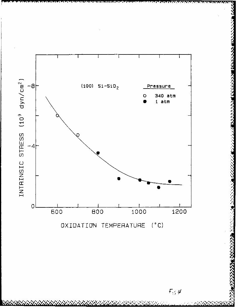
components is evident. Figure 4 shows a1 which is the difference
in the total and thermal stress against oxidation temperature. "
oi is seen to decrease with increasing oxidation temperature.
The origin and temperature dependence of a, is understood by
considering the large molar volume change, nV, for the conversion
of Si to SiO, and the viscoelastic nature of SiOg (14-16). From
figure 5, we see that the as-formed SiO occupies a greater
volume than the Si from which it was produced, hence an expansion
needs to occur into the free volume direction above the oxidizing
Si -urface. Using a Maxwell model for SiO, the rate at which
the flow cf SiO, can occur into this free direction is determined'
10i

by the SiQ2 viscosity, rj. At high oxidation temperatures where rA
is sufficiently small, the SiOa flows readily into the free
direction with a short relaxation time relative to the time for
oxidation. At lower temperatures, (below about 9000C), however,
Y is too large for complete relaxation, hence a, develops. The
lower is To., the higher is rj, and the higher is a,. Relaxation
time calculations seem to confirm this viscoelastic model for
SiO, (14).
In terms of the relationship of a, to Si oxidation models,
two different ideas have arisen. The first deals with the
compressive a, in the SiOa film. This compression ought to
reduce the diffusivity of 0., hence the supply of Oa to fuel the
oxidation reaction. Thus a decrease in the oxidation rate should
occur due to a,. Some confirmation for this exists from recent
experiments (26) that show that when a, is released by long term
annealing of thick SiO films, the oxidation rate increases.
Considering the molar volume change as the origin of a,, the
stress distribution in the SiO, film should result in a large
stress near the Si-Si02 interface with a decreasing stress
towards the SiO, surface. This would result in a higher a, and a
reduced oxidation rate for thinner SiOe films. However, it is
well known that a higher oxidation rate is seen for thin films
(less than 20 A), yet the shape of the thin SiO& oxidation data
is explained by this model (27-29). Most recent a, measurements
(20) have shown that indeed a higher stress exists for thinner
films, but not as high as would be required from these diffusion
01|
I-I-
....................................... ... ..

h.
models.
The second stress related oxidation model is derived from
the fact that the compressive a, in SiOa gives rise to a tensile
stress at the Si surface. The resulting strained Si bonds ought
to yield a more reactive Si surface thereby enhancing the rate of
oxidation(30). This idea seems in accord with the observation of
faster oxidation rates for thinner films, where the Si-SiO.
interface is kinetically most important, and some direct evidence
for an enhanced rate of oxidation for tensile loaded Si has been
presented (31). However, while there seems to be qualitative
agreement with the model, quantitative scaling of the oxidation
rate with a, is not found (32,33) and the predicted orientation
dependence for the stress is not observed (18).
From Figure 6, it is seen that the intrinsic stresses for
the (100), (110) and (311) Si orientations are near to each other
and larger than the stress in the (111) surface. The order for
oxidation rate (30,32,33) at the outset of oxidation is:(110) > (111) > (311) > (100)
However, after several tens of nm SiOs growth, the order changes
to:
(111) > (110) > (311) > (100)-
The initial oxidation regime scales qualitatively with the number
density of Si atoms in the various Si orientations, but after
this regime, the change in order may be a result of the reduced
compressive stress in the SiO,, since the scaling then appears t-
be in the order of smaller stress higher oxidaticin r te 33).
12

Since the initial oxidation rate does not scale quantitatively
with the number density of Si atoms, and a crossover in rate
order occurs for greater film thicknesses, a role for stress in
the oxidation mechanism can be envisaged, but it should be clear
that any definitive statements about the role of ar, on Si SC
oxidation kinetics requires further investigation.
Impurity Effects on Si Oxidation
It has long been recognized (6,7) that a variety of
impurities can alter the rate of Si oxidation, the mechanism for
oxidation, and in many cases the resultant interfacial Si-SiOa
electronic properties. One difficulty with the detailed
investigation of these effects is that the chemical analyses used
to identify and quantify many of the affecting impurities is far
less sensitive to the impurity than is the electronic property or
oxidation rate which is altered as a result of the presence of an
impurity. However, while the oxidation rate and electronic
effects are sensitive, they are not specific and thus there has
been great difficulty in establishing clear cause and effect
relationships. A similar situation surrounds our understanding
of the details of the cleaning process of semiconductor surfaces.
Virtually all common semiconductors are subjected to wet and/or
dry chemical processes prior to commencing the device fabrication
process ( 34-26). This exposure is usuaLly termed "cleaning" and
the intent is to remove any impurities. However, it is well
known that. for many of the cases examined, some impurities ai-ie
,N %%
.. %

indeed removed but often impurities are merely replaced. The
success of such a cleaning process relies on the innocuous nature
of replacement impurities.
Some recent research in the area of impurities and impurity
effects suggests that sensitive analytical techniques applied
during the cleaning process, so called "in-situ" analysis should
prove useful in elucidating the area of semiconductor surface
cleaning and the role of impurities (7,8,37). Among the
techniques explored and herein reported are in-situ ellipsometry
and in-situ contact angle used in the solution cleaning
environment of Si.
In-situ Solution Techniques
A. Ellipsometry. Ellipsometry is known to be sensitive to
submonolayer coverage of a surface (38). The measurables in
ellipsometry are the amplitude change in the light upon
reflection, IF, and the phase change, A. The measurables are
related to the other parameters of the reflection problem as:
tan'Fexp(i6) = f(nA, nF, no, X, p) (6)
where the n's are refractive indices (which are in general
complex) for the ambient, A, film, F and substrate, S,
respectively and X is the wavelength, L,, the film thickness and
(p the angle of incidence. Usually nA, no, p, and X are known.
Thus from a single measurement of IF and ,, nF and LF are obtained
a3suming that nF is real. Figure 7 shows the fused silica sample ,
cell used for the in situ measurements. Alignment of this cell
with sample vertical in the solution was a non trivial prccedure ,
14 ".
% I R %

KWUR'UWXW W.,.. a. , Srv US, P1 Xy29 LM. Wn 19n Arl PL2~JU U9' Pil fAn Ar wi P9 An1 N N I VI PVU9VW *~ V I u -is tvu
with the details in the literature (37).
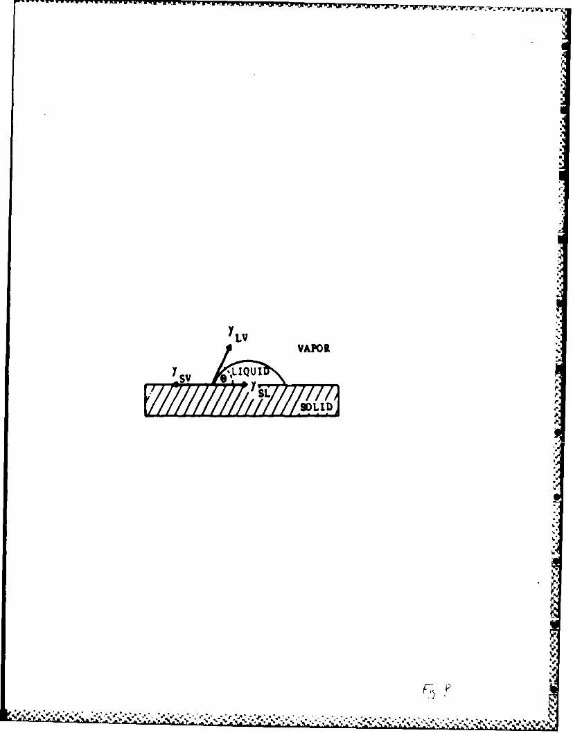
B. Contact Angle. The contact angle, e, is defined by the
equilibrium of three surface tension rectors, y1 , at the solid,
S, liquid, L, vapor, V, interface as y,, yB., YLV
cose = (Y9v - YL )/YLv (7)
Figure 8 shows the relationship. Usually only YLV is known for a
liquid, so that since e is measured only the difference yov - YOL
is obtained. Yet the wetting behavior of solids is directly
related to 9 where large angles indicate hydrophobic behavior N
(non wetting) and small angles hydrophilic behavior (wetting).
Most metals, oxides, and semiconductors are high energy solids
with surface tensions, YS 's, of from 500 to 5000 dynes/cm.
Waxes and some polymers are low energy solids with surface
tensions of less than 100 dynes/cm.. Virtually all liquids,
except liquid metals, have surface tensions less than 100
dynes/cm. From these values, it can be argued on thermodynamic
grounds that virtually all liquids will wet most solids, so as to
lower the surface energy of the solid and thus yield a small,
hydrophilic 8. It has been shown that the critical surface
tension, y., obtained when cose = 1 and thus y yLV (Yav
ys ) is specifically related to the surface structure and
composition of a solid surface (39).
For the measurement of 0 on semiconductor surfaces, during
cleaning, and with the surface protected from the atmosphere, an
inverted bubble technique (40) was adapted. The apparatus used
for the experimental results and the experimental details are
15
- -J .. .( 'p.*."*p.'.p. ~ V 5". ~. V'.'.~*4.~v . ' 0.

F
reported elsewhere (37). A gas bubble (Na) can be released from
the capillary and when held at the solid surface will establish
the three phase equilibrium. It is important to realize that
even though the bubble her-e .= gas, the contact angle measured is
the same as for the case shown in Figure 8
Results of In-situ Ellipsometric and Contact Angle Measurements
The first experimental result makes use of in-situ
ellipsometry to follow the process of HF etching of SiOa on Si.
The use of HF in Si technology is widespread for both the'p.
patterning and complete removal of SiOa from Si and the pre
processing cleaning step to remove a contaminated or damaged
native SiOa film. Furthermore, it is established that the
exposure of Si to HF alters the oxidation rate of Si(7,37). The
use of HF is an integral part of the successful cleaning of Si.
It is anticipated that the etching process of SiOa in dilute HF
should be able to be followed using in-situ ellipsometry, and
Figure 9 shows the rather linear decrease in SiOa film thickness
with etch time. In this experiment, it was expected that the
bare Si surface would be reached. This seems not to be the case,
as a minimum of about 20A SiOa film thickness is reached, and it
even appears as if the oxide grows slightly. However, in order4
to correctly interpret these results, it must be remembered that
an ellipsometric model of the film covered surface is required
for the analysis of the T,6 data obtained during the etching
process. Up tc here, we have used model comprised of three
cumrporents: air SiOg film Si substrate and the T, n data is'p
.-7.
%
always interpreted in terms of a calculated SiO4 film thickness.
It is seen in Figure 9 that this model works quite well down to
about 20A but below this SiOa thickness, the situation is not as
clear. Using this simple model, the SiOa etching first nearly
ceases and then the SiOa grows. Neither of these events is
entirely plausible considering what we know about the virulence
of the HF attack on SiO,. If the y,A trajectory is tracked below
20A as the SiO film is removed, the situation becomes somewhat
clarified and this unmodeled data is shown in Fig. 10. The solid
line represents a theoretical calculation of , values for the
situation: air - SiOa film Si substrate. The zero SiO film
thickness, i.e. 4i, for a bare Si surface is about 178 ° , 10.50
and as SiO, grows, 6 decreases and y increases. The etch
experiment shown in Fig. 10 commenced at an SiOa film thickness
of 8Snm with a 4j,6 of about 1030, 15.50 and proceeds towards the
bare Si surface value with increasing W along the theoretical
curve (open circles). Excellent agreement is seen along this
line from 85 to about 2nm- However, near the 2nm ,A value, a
deviation from the theoretical curve is seen (triangles) with A
decreasing again and 4J increasing, but for 41 a much slower
increase than if the correct model included a growing SiOa film.
Thus, while a value of 2-3rnm for SiOa is obtained for the y,An
data in the triangle region, the data is seen to deviate
substantially from the theoretical curve for SiO, on Si and henceV
from the simple model for a film on a substrate. This strongly
2uggests that the model is not -:orrect and possibly that a
17
% %
L& ML'' *~~~~2'

hw
different film is growing on the Si surface which traces out a
different W,6 trajectory.
In the effort to better determine the nature of the new film
forming on the Si surface, in-situ contact angle measurements
have proven useful(37). First it was observed that the contact
angle, 9, on SiO, on Si was about 8' which indicates strong
hydrophilic behavior of SiOa as anticipated for a high energy
solid in contact with an essentially aqueous media. When e is
folluwed during HF in H8 0 etching of SiOa, an abrupt change from
80 to 780 occurs when the SiOa is thought to be removed (near 2nm
SiOa ). The abrupt change from hydrophilic to hydrophobic
behavior is a commonplace observation in HF treatment of a SiOe
covered Si surface(42). However, based on what we know about the
surface energy of Si, namely it is high, the bare Si surface
should be hydrophilic as is SiOd, and thus no abrupt change in e
is expected. We conclude that there is something else on the Si
surface, something other than SiO or bare Si. In order to
elucidate the nature of the hydrophobic Si surface resulting from
HF exposure, the critical surface tension Yc was measured. For
this purpose, a plot of measured cose versus y, is obtained on
the Si surface in contact with a number of liquids with various
YLv and all with HF. This was done using solutions of HgO-CH3 OH
all with 1% HF. yuv varied from 72 dynes/cm for pure HaO to 23
dynes/cm for pure HF. Figure 11 shows the plot. First it is
seen that the plot is not linear. This has been shown to be the
catse whenever H bonding between Liquid and s-olid can occur (40)
N
*%a%"... .. • ..- *-.- " .- . .. - . - . ** ,* .. .. . .. -""

which is expected for HaO-CHjCOH solutions. More importantly is
the extrapolated value of y. = 27 dynes/cm for cosO = 1. A
comparison with literature values of y, leads to the conclusion
that the new film on Si is either a hydrocarbon and/or
fluorocarbon species. Since F is present and indeed crucial, and
F-C bonds are polar enough to cause H bonding between Si and
liquid, we conclude that a fluorocarbon is adsorbed on the Si
surface.
It is interesting that this fluorcarbon film on Si renders
the surface hydrophobic thereby likely precluding much foreign
and potentially degrading impurities from attaching to an
otherwise high energy Si surface. In addition, this treatment
leads to clean MOS devices. The effect of a final HF treatment
is essentially to yield the largest oxidation rate in comparison
with other accepted cleaning solutions, e.g., HaOa, HCI, NH.*OH
(8). It is not yet known why this is the case and other effects
of HF have not been determined, e.g. any long term effects of
residual F after thermal oxidation.
Summary P
The details of the mechanism for the reaction between Si and
oxidant to form an SiOa film is complex with many aspects:.
chemical, mechanical, electrical, morphological etc.. ManyP
eviews on silicon oxidation have treated the problem in detail. e
The present paper focuses on two very recent results, namely
mechanical intrinsic film stress implications and impurity
.'e4-
19 S.

effects on the oxidation mechanism. For these new studies, novel
techniques were used and are in themselves interesting means to
study surface films. The results, while by no means have settled
the major issues, have helped to gain further insight into the
important problem of the mechanism for Si oxidation.
Acknowledgement
The author is indebted to G. Gould and E. Kobeda for access
to their original data and for helpful discussions. This work was
supported in part by the Office of Naval Research, ONR.
20.
J.J.
References
1. E.A. Irene, Semiconductor International, April 1983, p. 99.
2. E.A. Irene, Semiconductor International, June 1985, p. 92.
3. B.E. Deal and A.S. Grove, J. Appi. Phys., 36 3770 (1965).
4. W.A. Pliskin, IBM J. Res. Dev., I0 198 (1966). 1
5. E.A. Irene and Y.J. van der Meulen, J. Electrochem. Soc., 123,
1380 (1976).
6. A.G. Revesz and R.J. Evans, J. Phys. Chem. Solids, 30 551(1969).
7. F.N. Schwettmann, K.L. Chiang and W.A. Brown, 153rdElectrochem. Soc. Meeting, Abs. #276, May 1978. .
8. G. Gould and E.A. Irene, J. Electrochem. Soc., 134, 1031
(1987).
9. E.A. Irene, Phil. Mag. B, 5, 131 (1987).
10. E.A. Irene, CRC Reviews in Solid State and Materials Science,
"Models for the Oxidation of Silicon," in press 1987.
11. R.J. Jaccodine and W.A. Schlegel, J. Appi. Phys., 37 2429(1966).
12. M.V. Whelan, A.H. Gormans and L.M. Goossens, Appl. Phys.Lett., 10 262 (1967).
13. E.P. EerNisse, AppI. Phys. Lett., 7i, 290 (1977); 35, 8
(1979).
14. E.A. Irene, E. Tierney and J. Angillelo, J. Electrochem. Soc.
129. 2594 (1982).
15. T.Y. Tan and U. Goesele, Appi. Phys. Lett., 39, 86 (1981); 46ib (1982).
16. W.A. Ti)ler, J. Electrochem. Soc., 128, 689 (1981).
17. E. Kobeda and E.A. Irene, J. Vac. Sci. Technol. B, 4j 720(1986 ). -
18. E. Kobeda and E.A. Irene, J. Vac. Sci. Technol. B, 5, 15 %(1987). '
13. G.G. Stoney, Proc. R. Soc., London Ser. A 2, 172 (1909).
20. E. Kobeda and L.A. Irene, J. Vac. Soc. B., to be pubLished 1987.
j=

21. G.A. Rozgonzi and D.C. Miller, Thin Solid Films, 31, 185(1976).
22. A. Segmuller, J. Angillelo, S.J. La Placa, J. Appl. Phys., 5_,6224 (1980).
23. A.G. Blachman, Metal. Trans., , 699 (1971).
24. E.A. Irene, J. Electronic Mat., 5, 287 (1976).
25. A.K. Sinha, H.J. Levinstein, and T.E. Smith, J. Appl. Phys.,49, 2423 (1985).
26. J.K. Srivastava and E.A. Irene, J. Electrochemical Soc., 132,
2815 (1985).
27. A. Fargeix, G. Ghibaudo and G. Kamarinos, J. Appl. Phys., _,2878 (1983); 54, 7153 (1983); 56 589 (1984).
28. G. Camera Roda, F. Santarelli and G.C. Sarti, J. Electrochem.Soc., 132, 1909 (1985).
29. R.H. Doremus, Thin Solid Films, 122 191 (1984).
30. E.A. Irene, H.Z. Massoud and E. Tierney, J. Electrochem. Soc.,133, 1253 (1986).
31. C.K. Huang, R.J. Jaccodine and S.R. Butler, Abs. 34,Electrochemical Society Meeting, Extend. Abstracts, Vol. 86-2,San Diego, CA, Oct. 19-24 (1986).
32. E.A. Lewis, E. Kobeda and E.A. Irene, "Proceedings of FifthInternational Symposium on Silicon Materials Science andProcessing," Ed. H.R. Huff, Boston, Mass., May 1986.
33. E.A. Lewis and E.A.Irene, J. Electrochem. Soc., 134, 23321,387.
33. E.A. Irene, H.Z. Massoud and E. Tierney, J. Electrochem. Soc.,13 1253 (1986).
34. W. Kern, Semiconductor International, p. 94, April 1984.
35. B.F. Phillips, D.C. Burkman, W.R. Schmidt and C.A. Petersen, J.Vac. Sci. Technol. A, 1 646 (1983).
A6. R.C. Henderson, J. Electrochemical Soc., 119, 772 (1972).
37. G. Gould and E.A. Irene, ;. Electrochem. Soc., submitted 1987.
J8. R.M.A. Azzam and N.M. Bashara, "Ellipsometry and PolarizedLight," North Holland Publishing Co., New York (1977).
39. Zisman, "Contact Angle: Wetability and Adhesion," Advances in
%S0 ~ ~ ' 9 % W %

Chemistry Series Vol. 43, Ed. F.M. Fowkes, American Chem. JoG.
Washington, DC (1964), Chap. I.
40. D. McLachlan Jr., and H.M. Cox, Rev. Sci. Instrum., 46 80
41. E.A. Irene, Phil. Mag. B. , 5, 131 (1937).
42. R. Williams and A.M. Goodman, App. Phys. Lett., ;b t)-3 ( 1374.
e.,
I-o
List of Figures
Figure 1. A schematic summary of F(T) versus oxidationtemperature, T.., where F(T) are the various oxidationtemperature sensitive properties for SiO, such as: refractiveindex, density, intrinsic stress, interface fixed charge,and interface trapped charge. (after ref. (41) and withpermission of Phil. Mag. ).
Figure 2. Parallel laser beam apparatus for the measurement ofwafer curvature. BS is a beamsplitter and MS is a flat mirror.
(after ref. (17) and with permission of the American VacuumSociety).
Figure 3. Total measured SiOe film stress and calculatedthermal expansion stress for various oxidation temperatures forSiOa grown on Si in dry 0&. (after ref. (17) and with permissionof the American Vacuum Society.)
Figure 4. Intinsic film stress versus oxidation temperaturesfor SiOD film grown on Si in dry O. (after ref. (17) and withpermission of the American Vacuum Society.)
Figure 5. Pictorial representation of viscous flow in SiO. as aresult of the molar volume change for the reaction of Si + 0, =
SiOs (after ref. (14) and with permission of the ElectrochemicalSociety, Inc.)
Figure 6. Intrinsic stress for a SiO. film on Si versusoxidation temperature in dry O at one atm. for various Siorientations (after ref. (18) and with permission of the AmericanVacuum Society).
Figure 7. Fused silica sample cell used for in-situellipsometric measurements. (after ref. (37)).
Figure 8. Representation of the important surface tensionrectors, yj, for the equilibrium between solid, S, liquid, L,and vapor, V, and with 9 as the contact angle. (after ref.(37)).
Figure 9. SiOa film thickness versus etch time in HF-higOsolution from in-situ ellipsometry measurements (after ref.
(37)).
Figure 10. '-vs-A trajectories for the etching of an 85nm SiO,film in HF-HRO sotution (after ref. (37)).
Figure 11. cosG-vs-y plot of SiO, on Si in various CH 3OH-HO-HF solutions. ye is shown at cosO = 1 to be 27 dynes/cm. (after
ref. (37)). IA41 -
*.d- -.- - - . .

SiO2 FILM PROPERTIES, F(T), VERSUS OXIDATION
TEMPERATURE, Tox
OX/
5..
F(T)a!'a'.
I.%
ANNEAL
(950 - 105000
F(T)INTRINSIC STRESS
DENSITY _'
REFRACTIVE INDEX N
FIXED OXIDE CHARGE FF
INTERFACE TRAPPED CHARGEQ i.
.
...-7 5. * % F"t*, , A *, .*'5*' .

Ww I 'w FR M F -WvWw Y VRIFV Yw
laserBS1
2H
IwI
sc e n 3 .5,
7--p
sample
translation stage

I I I I I I i
16"M
-8 (100) si-sio2
------TOTAL FILM STRESS
-0-- THERMAL EXPANSION STRESSC~i -6 -
u
o -40
U)
LU -2-
U)
0
I I [ , I I I I
600 800 1000 1200
OXIDATION TEMPERATURE (°C) S
'S
op
CI--
E -8- (±00) si-SiO 2 Pressureu
"1,0 340 atmC0 i atm
L
z
H
600 600 1000 1200
OXIOAT1fJN TEMPERATURE (0C)
'W
A~
%5

op
SiO 2 FLOW
COMPRESSIVESTRESS
y

c:7''
u
,0
0 100
wcc
zcc
z
700 800 900 1000 1100
TEMPERATURE (OC)

. . .. ....
r-
-LVW.v.,dJ-Vii.U
VAPOR
%,LIQU
svp
k ___J
LID-

WWT~rWVWV " WWV nW~U~rrI VW" wvvWVMIPIWIiV wwijWWV~ I WP3WAUJ . jr w- vw Vj
A
a,
00.
0 z
00
0
0~~000 00 40 6o to 10 0
TIME (MINUTES)

PSI vs. DELTA FOR HF ETCH EXPERIMENTS
It I I I I i
CALCULATED ZERO 0 ETCH BACKOXIDE THICKNESS A LAYER GROWTH
--- THEORETICALI30 CURVE
S160-LU EXPERIMENTALui LAYER
"L- MINIMUM OXIDELo GROWTH 'D R THICKNESS: 2nm
140 o
J 0 INITIAL OXIDELUIw 120 A! THICKNESS: 85nm
A ETCHING100 A0
., I I I I I,
0 2 4 6 8 10 12 14 16
PSI (DEGREES)
-a
-j 0
,, , ?'Z%. /. :, ,'., ,. '.. ., % .,.. .;.; .., .,;,,..., - -v " ".. .-. .-.- ... ,-,-.- . ,',

li-u li• " • AU • • ' I •
16
0.6
0.2--
0.0 ; I ,20 25 30 35 40 45 50 55 60 65 70 75
LV SUnF. TENS. IdYnes/cB)
I'k
Ui

M.9 ~ ~~WX ~WLW ~ Y~w~y~ ~-~j -~ ~ w ~ - ~*
I.
i
i..
ILMED4.
~cp
"p
h
* 4~~: i~~%~\ ~ ~ 1 .~* ~ - P P -P. * ~ ~ -- ~. -P *~
~J ~pI*.~ ~ -.P., P, P~* PP~**P~P~ * -