7 series fpgas memory interface solutions - xilinx.com · the following table shows the revision...
TRANSCRIPT

7 Series FPGAs Memory Interface Solutions
User Guide
UG586 March 1, 2011
7 Series FPGAs Memory Interface Solutions www.xilinx.com UG586 March 1, 2011
Xilinx is providing this product documentation, hereinafter “Information,” to you “AS IS” with no warranty of any kind, express or implied. Xilinx makes no representation that the Information, or any particular implementation thereof, is free from any claims of infringement. You are responsible for obtaining any rights you may require for any implementation based on the Information. All specifications are subject to change without notice.
XILINX EXPRESSLY DISCLAIMS ANY WARRANTY WHATSOEVER WITH RESPECT TO THE ADEQUACY OF THE INFORMATION OR ANY IMPLEMENTATION BASED THEREON, INCLUDING BUT NOT LIMITED TO ANY WARRANTIES OR REPRESENTATIONS THAT THIS IMPLEMENTATION IS FREE FROM CLAIMS OF INFRINGEMENT AND ANY IMPLIED WARRANTIES OF MERCHANTABILITY OR FITNESS FOR A PARTICULAR PURPOSE.
Except as stated herein, none of the Information may be copied, reproduced, distributed, republished, downloaded, displayed, posted, or transmitted in any form or by any means including, but not limited to, electronic, mechanical, photocopying, recording, or otherwise, without the prior written consent of Xilinx.
© Copyright 2010 Xilinx, Inc. XILINX, the Xilinx logo, Virtex, Kintex, Artix, Spartan, ISE, and other designated brands included herein are trademarks of Xilinx in the United States and other countries. AMBA is a registered trademark of ARM in the EU and other countries. All other trademarks are the property of their respective owners.
Revision HistoryThe following table shows the revision history for this document.
Date Version Revision
03/01/11 1.0 Xilinx Initial Release.
7 Series FPGAs Memory Interface Solutions www.xilinx.com 3UG586 March 1, 2011
Revision History . . . . . . . . . . . . . . . . . . . . . . . . . . . . . . . . . . . . . . . . . . . . . . . . . . . . . . . . . . . . . 2
Preface: About This GuideGuide Contents . . . . . . . . . . . . . . . . . . . . . . . . . . . . . . . . . . . . . . . . . . . . . . . . . . . . . . . . . . . . . . 5References . . . . . . . . . . . . . . . . . . . . . . . . . . . . . . . . . . . . . . . . . . . . . . . . . . . . . . . . . . . . . . . . . . . 5Additional Resources . . . . . . . . . . . . . . . . . . . . . . . . . . . . . . . . . . . . . . . . . . . . . . . . . . . . . . . . 6Conventions . . . . . . . . . . . . . . . . . . . . . . . . . . . . . . . . . . . . . . . . . . . . . . . . . . . . . . . . . . . . . . . . . 6
Typographical . . . . . . . . . . . . . . . . . . . . . . . . . . . . . . . . . . . . . . . . . . . . . . . . . . . . . . . . . . . . . 6Online Document . . . . . . . . . . . . . . . . . . . . . . . . . . . . . . . . . . . . . . . . . . . . . . . . . . . . . . . . . . 7
List of Acronyms . . . . . . . . . . . . . . . . . . . . . . . . . . . . . . . . . . . . . . . . . . . . . . . . . . . . . . . . . . . . . 7
Chapter 1: DDR3 SDRAM Memory Interface SolutionIntroduction . . . . . . . . . . . . . . . . . . . . . . . . . . . . . . . . . . . . . . . . . . . . . . . . . . . . . . . . . . . . . . . . . 9New Features . . . . . . . . . . . . . . . . . . . . . . . . . . . . . . . . . . . . . . . . . . . . . . . . . . . . . . . . . . . . . . . . 9Getting Started with the CORE Generator Software. . . . . . . . . . . . . . . . . . . . . . . . . . . 9
System Requirements . . . . . . . . . . . . . . . . . . . . . . . . . . . . . . . . . . . . . . . . . . . . . . . . . . . . . . 9Customizing and Generating the Core . . . . . . . . . . . . . . . . . . . . . . . . . . . . . . . . . . . . . . . 10Creating 7 Series FPGA DDR3 Memory Controller Block Design . . . . . . . . . . . . . . . . 18Directory Structure and File Descriptions . . . . . . . . . . . . . . . . . . . . . . . . . . . . . . . . . . . . 31Quick Start Example Design. . . . . . . . . . . . . . . . . . . . . . . . . . . . . . . . . . . . . . . . . . . . . . . . 36Modifying the Example Design . . . . . . . . . . . . . . . . . . . . . . . . . . . . . . . . . . . . . . . . . . . . . 39
Getting Started with EDK . . . . . . . . . . . . . . . . . . . . . . . . . . . . . . . . . . . . . . . . . . . . . . . . . . . 48Core Architecture . . . . . . . . . . . . . . . . . . . . . . . . . . . . . . . . . . . . . . . . . . . . . . . . . . . . . . . . . . . 48
Overview . . . . . . . . . . . . . . . . . . . . . . . . . . . . . . . . . . . . . . . . . . . . . . . . . . . . . . . . . . . . . . . . 48User Interface . . . . . . . . . . . . . . . . . . . . . . . . . . . . . . . . . . . . . . . . . . . . . . . . . . . . . . . . . . . . 50AXI4 Slave Interface Block . . . . . . . . . . . . . . . . . . . . . . . . . . . . . . . . . . . . . . . . . . . . . . . . . 53Arbitration in AXI Shim . . . . . . . . . . . . . . . . . . . . . . . . . . . . . . . . . . . . . . . . . . . . . . . . . . . 56User Interface Block . . . . . . . . . . . . . . . . . . . . . . . . . . . . . . . . . . . . . . . . . . . . . . . . . . . . . . . 57Native Interface . . . . . . . . . . . . . . . . . . . . . . . . . . . . . . . . . . . . . . . . . . . . . . . . . . . . . . . . . . 57Clocking Architecture . . . . . . . . . . . . . . . . . . . . . . . . . . . . . . . . . . . . . . . . . . . . . . . . . . . . . 60Memory Controller . . . . . . . . . . . . . . . . . . . . . . . . . . . . . . . . . . . . . . . . . . . . . . . . . . . . . . . 63PHY . . . . . . . . . . . . . . . . . . . . . . . . . . . . . . . . . . . . . . . . . . . . . . . . . . . . . . . . . . . . . . . . . . . . 66
Designing with the Core . . . . . . . . . . . . . . . . . . . . . . . . . . . . . . . . . . . . . . . . . . . . . . . . . . . . 89Interfacing to the Core . . . . . . . . . . . . . . . . . . . . . . . . . . . . . . . . . . . . . . . . . . . . . . . . . . . . . . 89
AXI4 Slave Interface . . . . . . . . . . . . . . . . . . . . . . . . . . . . . . . . . . . . . . . . . . . . . . . . . . . . . . 89AXI addressing . . . . . . . . . . . . . . . . . . . . . . . . . . . . . . . . . . . . . . . . . . . . . . . . . . . . . . . . . . . 89User Interface . . . . . . . . . . . . . . . . . . . . . . . . . . . . . . . . . . . . . . . . . . . . . . . . . . . . . . . . . . . . 89Native Interface . . . . . . . . . . . . . . . . . . . . . . . . . . . . . . . . . . . . . . . . . . . . . . . . . . . . . . . . . . 95Physical Layer Interface (Non-Memory Controller design) . . . . . . . . . . . . . . . . . . . . . 96
Customizing the Core . . . . . . . . . . . . . . . . . . . . . . . . . . . . . . . . . . . . . . . . . . . . . . . . . . . . . . . 97Design Guidelines . . . . . . . . . . . . . . . . . . . . . . . . . . . . . . . . . . . . . . . . . . . . . . . . . . . . . . . . . 102
DDR3 SDRAM . . . . . . . . . . . . . . . . . . . . . . . . . . . . . . . . . . . . . . . . . . . . . . . . . . . . . . . . . . 102Supported Devices for 7 Series FPGAs. . . . . . . . . . . . . . . . . . . . . . . . . . . . . . . . . . . . . . 123
Table of Contents
4 www.xilinx.com 7 Series FPGAs Memory Interface SolutionsUG586 March 1, 2011
Chapter 2: QDRII+ Memory Interface SolutionIntroduction . . . . . . . . . . . . . . . . . . . . . . . . . . . . . . . . . . . . . . . . . . . . . . . . . . . . . . . . . . . . . . . 125Getting Started with the CORE Generator Software. . . . . . . . . . . . . . . . . . . . . . . . . 125
System Requirements . . . . . . . . . . . . . . . . . . . . . . . . . . . . . . . . . . . . . . . . . . . . . . . . . . . . 125Customizing and Generating the Core . . . . . . . . . . . . . . . . . . . . . . . . . . . . . . . . . . . . . . 126Creating the 7 Series FPGA QDRII+ SRAM Memory Design . . . . . . . . . . . . . . . . . . . 134MIG Directory Structure and File Descriptions. . . . . . . . . . . . . . . . . . . . . . . . . . . . . . . 142
Core Architecture . . . . . . . . . . . . . . . . . . . . . . . . . . . . . . . . . . . . . . . . . . . . . . . . . . . . . . . . . . 146Overview . . . . . . . . . . . . . . . . . . . . . . . . . . . . . . . . . . . . . . . . . . . . . . . . . . . . . . . . . . . . . . . 146User Interface . . . . . . . . . . . . . . . . . . . . . . . . . . . . . . . . . . . . . . . . . . . . . . . . . . . . . . . . . . . 148Clocking Architecture . . . . . . . . . . . . . . . . . . . . . . . . . . . . . . . . . . . . . . . . . . . . . . . . . . . . 150Physical Interface . . . . . . . . . . . . . . . . . . . . . . . . . . . . . . . . . . . . . . . . . . . . . . . . . . . . . . . . 151Write Path . . . . . . . . . . . . . . . . . . . . . . . . . . . . . . . . . . . . . . . . . . . . . . . . . . . . . . . . . . . . . . 154Read path . . . . . . . . . . . . . . . . . . . . . . . . . . . . . . . . . . . . . . . . . . . . . . . . . . . . . . . . . . . . . . 156Calibration. . . . . . . . . . . . . . . . . . . . . . . . . . . . . . . . . . . . . . . . . . . . . . . . . . . . . . . . . . . . . . 157
Customizing the Core . . . . . . . . . . . . . . . . . . . . . . . . . . . . . . . . . . . . . . . . . . . . . . . . . . . . . . 160Design Guidelines . . . . . . . . . . . . . . . . . . . . . . . . . . . . . . . . . . . . . . . . . . . . . . . . . . . . . . . . . 161
Design Rules . . . . . . . . . . . . . . . . . . . . . . . . . . . . . . . . . . . . . . . . . . . . . . . . . . . . . . . . . . . . 161Trace Length Requirements . . . . . . . . . . . . . . . . . . . . . . . . . . . . . . . . . . . . . . . . . . . . . . . 161Pinout Requirements . . . . . . . . . . . . . . . . . . . . . . . . . . . . . . . . . . . . . . . . . . . . . . . . . . . . . 162I/O Standards . . . . . . . . . . . . . . . . . . . . . . . . . . . . . . . . . . . . . . . . . . . . . . . . . . . . . . . . . . . 163
7 Series FPGAs Memory Interface Solutions www.xilinx.com 5UG586 March 1, 2011
Preface
About This Guide
Xilinx® 7 series FPGAs include three unified FPGA families that are all designed for lowest power to enable a common design to scale across families for optimal power, performance, and cost. The Artix™-7 family is optimized for lowest cost and absolute power for the highest volume applications. The Virtex®-7 family is optimized for highest system performance and capacity. The Kintex™-7 family is an innovative class of FPGAs optimized for the best price-performance. This guide serves as a technical reference to using, customizing, and simulating LogiCORE™ IP DDR3 SDRAM memory interface cores for 7 series FPGAs.
Guide ContentsThis manual contains the following chapters:
• Chapter 1, DDR3 SDRAM Memory Interface Solution, describes the bank and pin rules for DDR3 SDRAM interfaces in 7 series FPGAs.
• Chapter 2, QDRII+ Memory Interface Solution describes the architecture of the 7 series FPGA QDRII+ memory interface core and provides details on customizing and interfacing to the core.
References1. UG471, 7 Series FPGAs SelectIO Resources User Guide
2. ARM® AMBA® Specificationshttp://www.arm.com/products/system-ip/amba/amba-open-specifications.php
3. JESD79-3E, DDR3 SDRAM Standard, JEDEC Solid State Technology Associationhttp://www.jedec.org/sites/default/files/docs/JESD79-3E.pdf
4. UG683, EDK Concepts, Tools, and Techniques
5. UG111, Embedded System Tools Reference Manual
6. TN-47-01, DDR2-533 Memory Design Guide For Two-DIMM Unbuffered Systems. Micron Technology, Inc.
7. ChipScope Pro Logic Analyzer toolhttp://www.xilinx.com/tools/cspro.htm
8. UG628, Command Line Tools User Guide, COMPXLIB
9. UG626, Synthesis and Simulation Design Guide
10. DS176, 7 Series FPGAs Memory Interface Solutions Data Sheet
11. PlanAhead™ Design Analysis toolhttp://www.xilinx.com/tools/planahead.htm
12. UG612, Xilinx Timing Constraints User Guide
6 www.xilinx.com 7 Series FPGAs Memory Interface SolutionsUG586 March 1, 2011
Preface: About This Guide
13. UG199, Virtex-5 FPGA ML561 Memory Interfaces Development Board User Guide
14. DS182, 7 Series FPGAs Data Sheet: DC and Switching Characteristics
15. UG029, ChipScope Pro 11.1 Software and Cores User Guide
16. "Improving DDR SDRAM Efficiency with a Reordering Controller" XCELL Journal Issue 69 www.xilinx.com/publications/archives/xcell/Xcell69.pdf
Additional ResourcesTo find additional documentation, see the Xilinx website at:
http://www.xilinx.com/support/documentation/index.htm.
To search the Answer Database of silicon, software, and IP questions and answers, or to create a technical support WebCase, see the Xilinx website at:
http://www.xilinx.com/support.
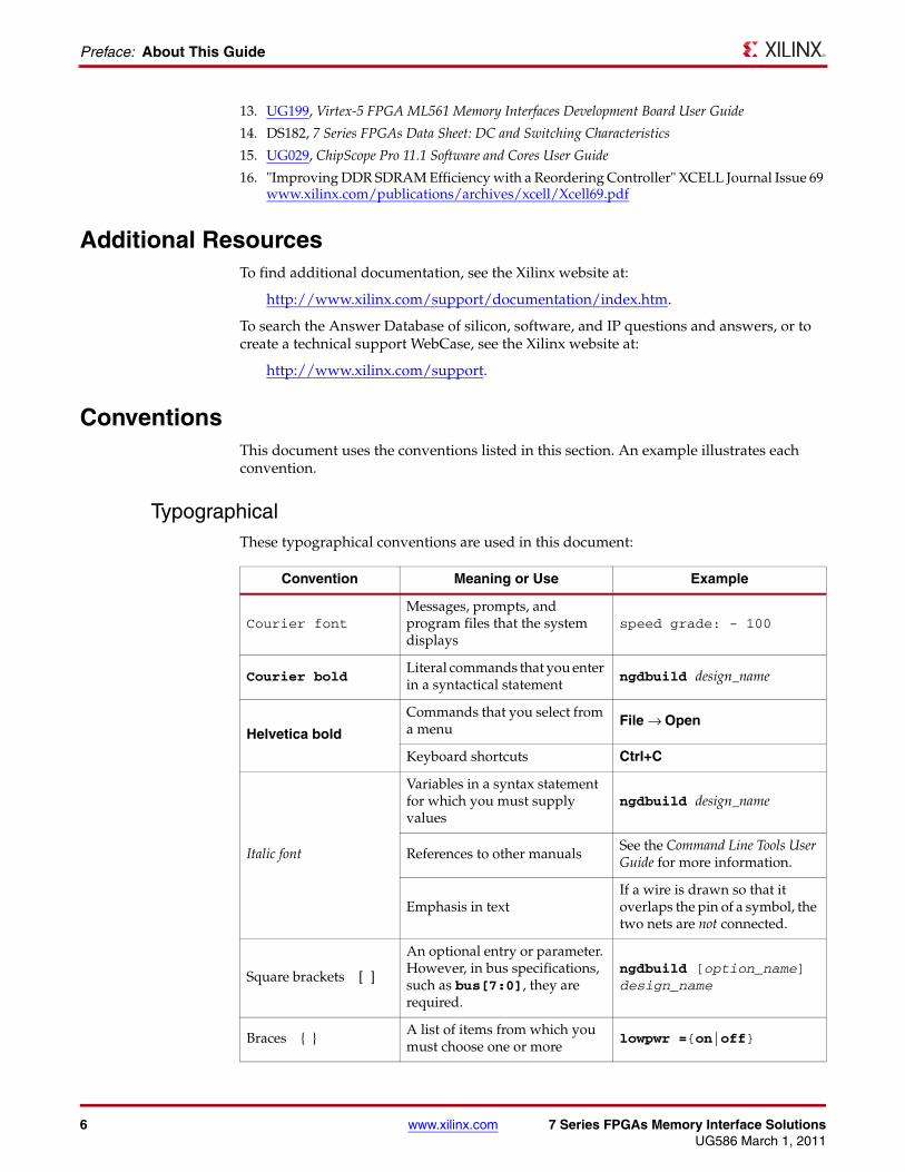
ConventionsThis document uses the conventions listed in this section. An example illustrates each convention.
TypographicalThese typographical conventions are used in this document:
Convention Meaning or Use Example
Courier fontMessages, prompts, and program files that the system displays
speed grade: - 100
Courier boldLiteral commands that you enter in a syntactical statement
ngdbuild design_name
Helvetica bold
Commands that you select from a menu
File → Open
Keyboard shortcuts Ctrl+C
Italic font
Variables in a syntax statement for which you must supply values
ngdbuild design_name
References to other manualsSee the Command Line Tools User Guide for more information.
Emphasis in textIf a wire is drawn so that it overlaps the pin of a symbol, the two nets are not connected.
Square brackets [ ]
An optional entry or parameter. However, in bus specifications, such as bus[7:0], they are required.
ngdbuild [option_name] design_name
Braces { }A list of items from which you must choose one or more
lowpwr ={on|off}
7 Series FPGAs Memory Interface Solutions www.xilinx.com 7UG586 March 1, 2011
List of Acronyms
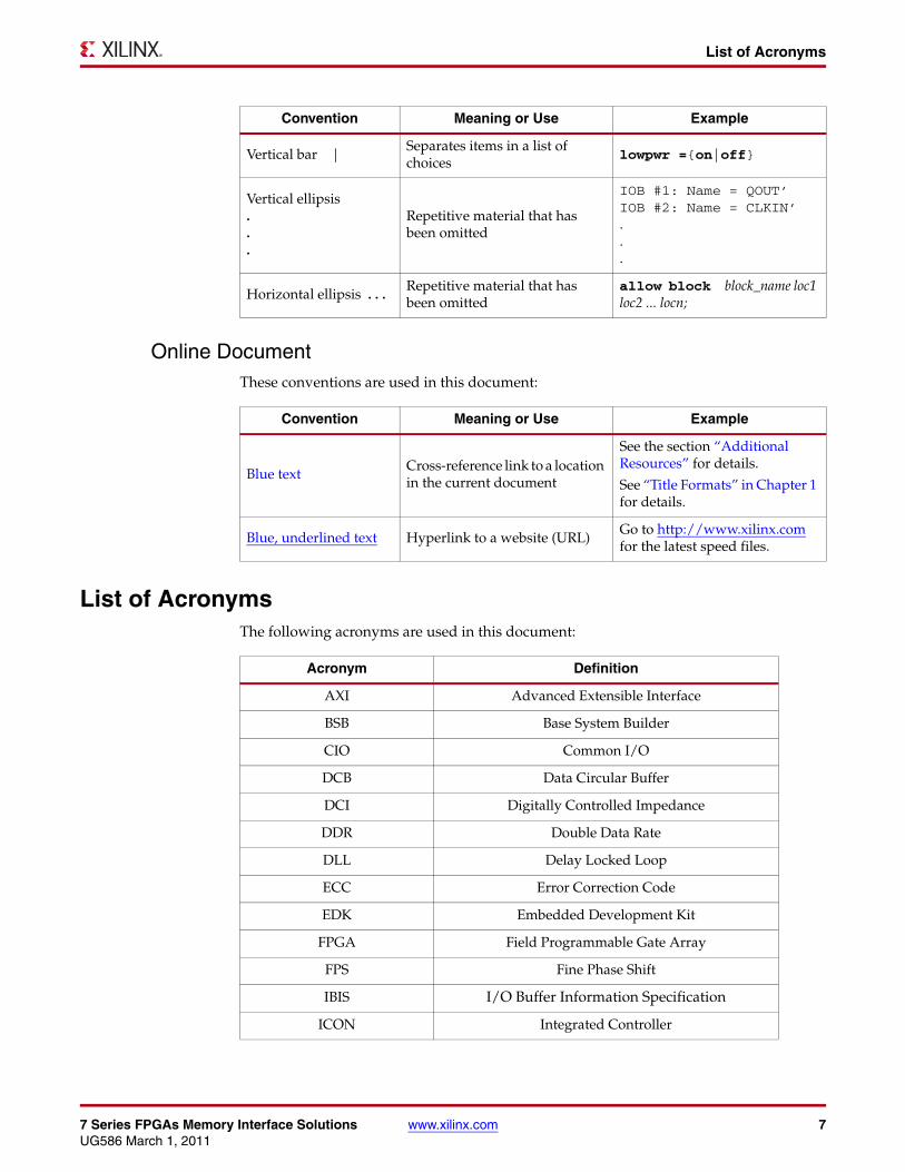
Online DocumentThese conventions are used in this document:
List of AcronymsThe following acronyms are used in this document:
Vertical bar |Separates items in a list of choices
lowpwr ={on|off}
Vertical ellipsis...
Repetitive material that has been omitted
IOB #1: Name = QOUT’ IOB #2: Name = CLKIN’...
Horizontal ellipsis . . .Repetitive material that has been omitted
allow block block_name loc1 loc2 ... locn;
Convention Meaning or Use Example
Convention Meaning or Use Example
Blue textCross-reference link to a location in the current document
See the section “Additional Resources” for details.
See “Title Formats” in Chapter 1 for details.
Blue, underlined text Hyperlink to a website (URL)Go to http://www.xilinx.com for the latest speed files.
Acronym Definition
AXI Advanced Extensible Interface
BSB Base System Builder
CIO Common I/O
DCB Data Circular Buffer
DCI Digitally Controlled Impedance
DDR Double Data Rate
DLL Delay Locked Loop
ECC Error Correction Code
EDK Embedded Development Kit
FPGA Field Programmable Gate Array
FPS Fine Phase Shift
IBIS I/O Buffer Information Specification
ICON Integrated Controller
8 www.xilinx.com 7 Series FPGAs Memory Interface SolutionsUG586 March 1, 2011
Preface: About This Guide
ILA Integrated Logic Analyzer
IOB Input/Output Block
LFSR Linear Feedback Shift Register
LUT Look-Up Table
MC Memory Controller
MIG Memory Interface Generator
MMCM Mixed-Mode Clock Manager
MRCC Multi-Region Clock Capable
MRS Mode Register Set
NOP No Operation
ODT On-Die Termination
OTF On the Fly
PHY Physical Layer
PRBS Pseudo Random Binary Sequence
QDR Quad Data Rate
RLDRAM Reduced-Latency Dynamic Random Access Memory
SDR Single Data Rate
SDRAM Synchronous Dynamic Random Access Memory
SPD Serial Presence Detect
SRAM Static Random Access Memory
SRCC Single-Region Clock Capable
SSO Simultaneous Switching Output
TDM Time Division Multiplexing
TIG Timing Ignore
UCF User Constraints File
UI User Interface
VCO Voltage Controlled Oscillator
VIO Virtual I/O
XPS Xilinx Platform Studio
Acronym Definition
7 Series FPGAs Memory Interface Solutions www.xilinx.com 9UG586 March 1, 2011
Chapter 1
DDR3 SDRAM Memory Interface Solution
IntroductionThe 7 series FPGAs memory interface solutions core is a combined pre-engineered controller and physical layer (PHY) for interfacing 7 series FPGA user designs and advanced extensible interface (AXI4) slave interfaces to DDR3 SDRAM devices. This user guide provides information about using, customizing, and simulating a LogiCORE™ IP DDR3 SDRAM memory interface core for 7 series FPGAs. In the Embedded Development Kit (EDK) this core is provided through the Xilinx® Platform Studio (XPS) as the axi_7series_ddrx IP with a static AXI4 to DDR3 SDRAM architecture. The user guide describes the core architecture and provides details on customizing and interfacing to the core.
Note: The current release of this solution supports DDR3 SDRAM and QDRII+ SRAM memory devices.
New FeaturesThe new features in the 7 series FPGA memory interface solutions are:
• Higher performance.
• New hardware blocks used in the physical layer: PHASER_IN and PHASER_OUT, PHY control block, and I/O FIFOs (see Core Architecture, page 48).
• Pinout rules changed due to the hardware blocks (see Design Guidelines, page 102).
• Controller and user interface operate at 1/4 the memory clock frequency.
Getting Started with the CORE Generator SoftwareThis section is a step-by-step guide for using the CORE Generator™ software to generate a DDR3 SDRAM memory interface in a 7 series FPGA, run the design through implementation with the Xilinx tools, and simulate the example design using the synthesizable test bench provided.
System Requirements• ISE® Design Suite, version 13.1
10 www.xilinx.com 7 Series FPGAs Memory Interface SolutionsUG586 March 1, 2011
Chapter 1: DDR3 SDRAM Memory Interface Solution
Customizing and Generating the Core
Generation through Graphical User Interface
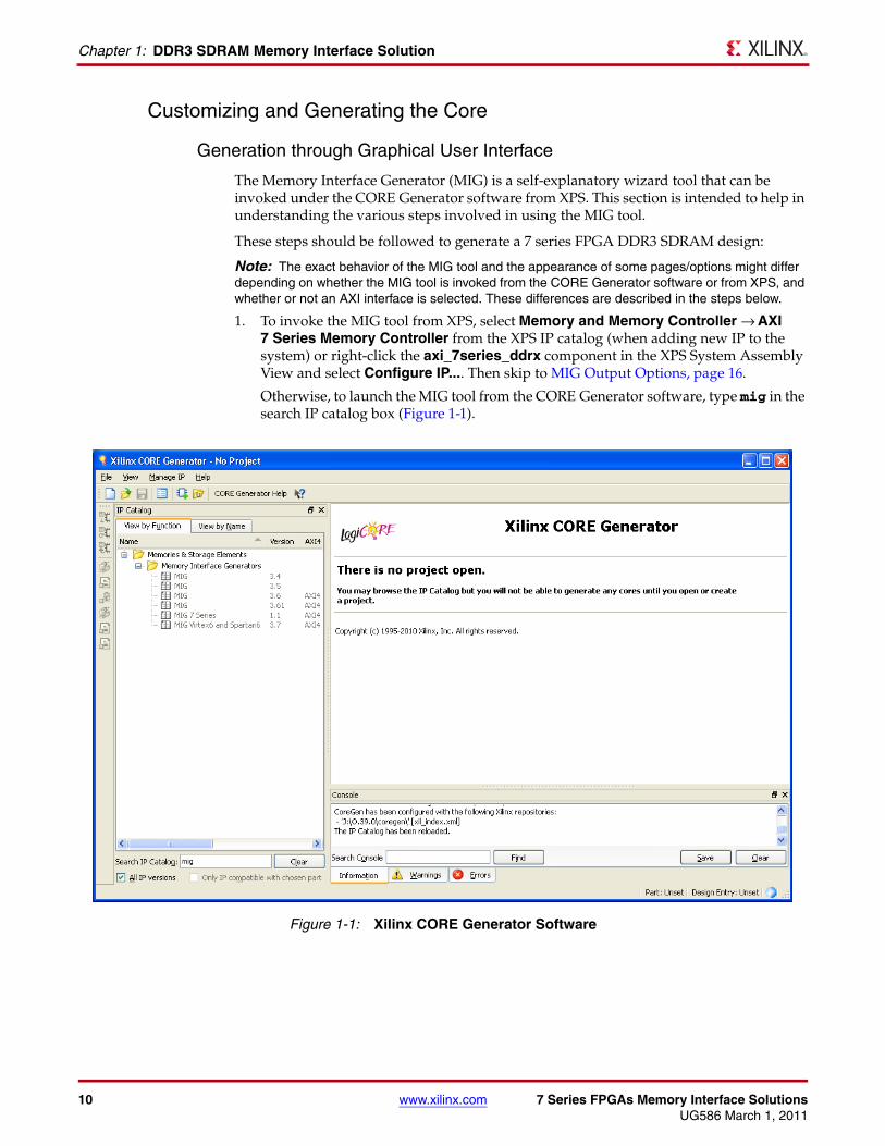
The Memory Interface Generator (MIG) is a self-explanatory wizard tool that can be invoked under the CORE Generator software from XPS. This section is intended to help in understanding the various steps involved in using the MIG tool.
These steps should be followed to generate a 7 series FPGA DDR3 SDRAM design:
Note: The exact behavior of the MIG tool and the appearance of some pages/options might differ depending on whether the MIG tool is invoked from the CORE Generator software or from XPS, and whether or not an AXI interface is selected. These differences are described in the steps below.
1. To invoke the MIG tool from XPS, select Memory and Memory Controller → AXI 7 Series Memory Controller from the XPS IP catalog (when adding new IP to the system) or right-click the axi_7series_ddrx component in the XPS System Assembly View and select Configure IP.... Then skip to MIG Output Options, page 16.
Otherwise, to launch the MIG tool from the CORE Generator software, type mig in the search IP catalog box (Figure 1-1).
X-Ref Target - Figure 1-1
Figure 1-1: Xilinx CORE Generator Software
7 Series FPGAs Memory Interface Solutions www.xilinx.com 11UG586 March 1, 2011
Getting Started with the CORE Generator Software
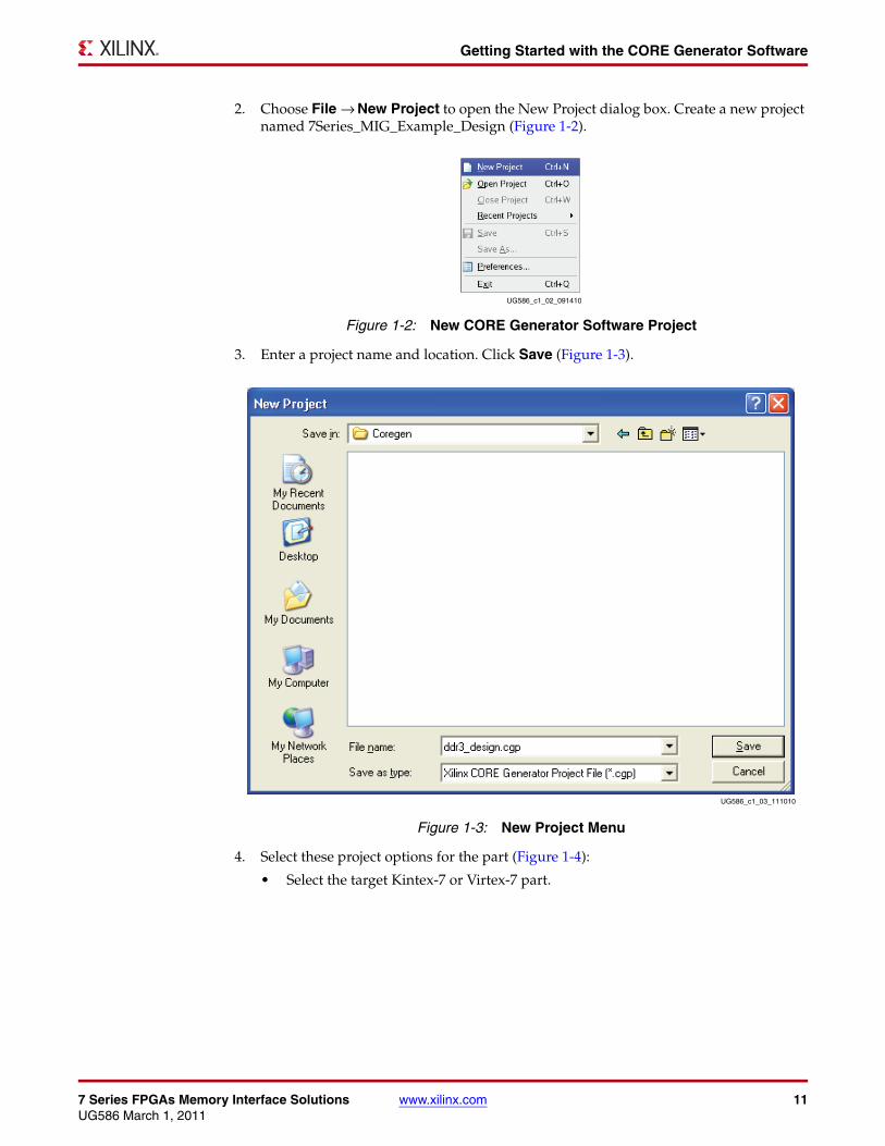
2. Choose File → New Project to open the New Project dialog box. Create a new project named 7Series_MIG_Example_Design (Figure 1-2).
3. Enter a project name and location. Click Save (Figure 1-3).
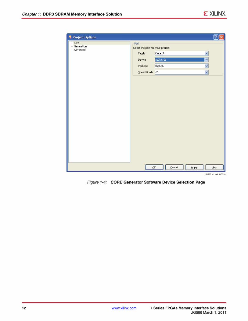
4. Select these project options for the part (Figure 1-4):
• Select the target Kintex-7 or Virtex-7 part.
X-Ref Target - Figure 1-2
Figure 1-2: New CORE Generator Software Project
X-Ref Target - Figure 1-3
Figure 1-3: New Project Menu
UG586_c1_02_091410
UG586_c1_03_111010
12 www.xilinx.com 7 Series FPGAs Memory Interface SolutionsUG586 March 1, 2011
Chapter 1: DDR3 SDRAM Memory Interface Solution
X-Ref Target - Figure 1-4
Figure 1-4: CORE Generator Software Device Selection Page
UG586_c1_04_110610
7 Series FPGAs Memory Interface Solutions www.xilinx.com 13UG586 March 1, 2011
Getting Started with the CORE Generator Software
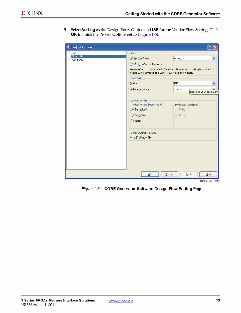
5. Select Verilog as the Design Entry Option and ISE for the Vendor Flow Setting. Click OK to finish the Project Options setup (Figure 1-5).
X-Ref Target - Figure 1-5
Figure 1-5: CORE Generator Software Design Flow Setting Page
UG586_c1_05_110610
14 www.xilinx.com 7 Series FPGAs Memory Interface SolutionsUG586 March 1, 2011
Chapter 1: DDR3 SDRAM Memory Interface Solution
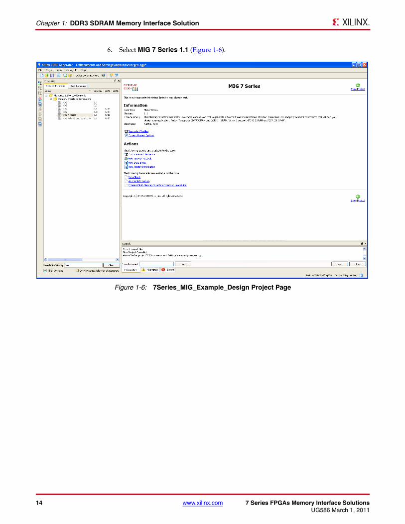
6. Select MIG 7 Series 1.1 (Figure 1-6).X-Ref Target - Figure 1-6
Figure 1-6: 7Series_MIG_Example_Design Project Page

7 Series FPGAs Memory Interface Solutions www.xilinx.com 15UG586 March 1, 2011
Getting Started with the CORE Generator Software
7. The options screen in the CORE Generator software displays the details of the selected CORE Generator software options that are selected before invoking the MIG tool (Figure 1-7).
8. Click Next to display the Output Options page.
X-Ref Target - Figure 1-7
Figure 1-7: 7 Series FPGA Memory Interface Generator Front Page
UG586_c1_08_110710

16 www.xilinx.com 7 Series FPGAs Memory Interface SolutionsUG586 March 1, 2011
Chapter 1: DDR3 SDRAM Memory Interface Solution
MIG Output Options
1. Select the Create Design radio button to create a new memory controller design. Enter a component name in the Component Name field (Figure 1-8).
MIG outputs are generated with the folder name <component name>.
Note: Only alphanumeric characters can be used for <component name>. Special characters cannot be used. This name should always start with an alphabetical character and can end with an alphanumeric character.
When invoked from XPS, the component name is corrected to be the IP instance name from XPS.
2. Click Next to display the Pin Compatible FPGAs page.
X-Ref Target - Figure 1-8
Figure 1-8: MIG Output Options
UG586_c1_09_110710
7 Series FPGAs Memory Interface Solutions www.xilinx.com 17UG586 March 1, 2011
Getting Started with the CORE Generator Software
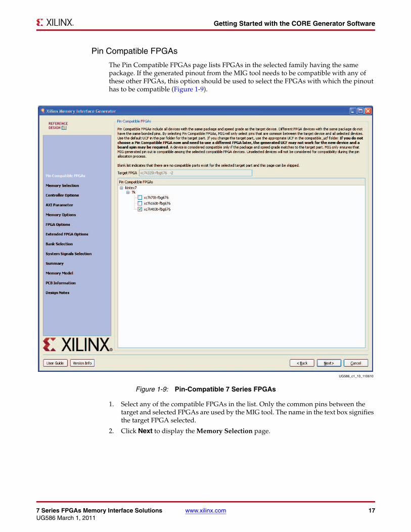
Pin Compatible FPGAs
The Pin Compatible FPGAs page lists FPGAs in the selected family having the same package. If the generated pinout from the MIG tool needs to be compatible with any of these other FPGAs, this option should be used to select the FPGAs with which the pinout has to be compatible (Figure 1-9).
1. Select any of the compatible FPGAs in the list. Only the common pins between the target and selected FPGAs are used by the MIG tool. The name in the text box signifies the target FPGA selected.
2. Click Next to display the Memory Selection page.
X-Ref Target - Figure 1-9
Figure 1-9: Pin-Compatible 7 Series FPGAs
UG586_c1_10_110610
18 www.xilinx.com 7 Series FPGAs Memory Interface SolutionsUG586 March 1, 2011
Chapter 1: DDR3 SDRAM Memory Interface Solution
Creating 7 Series FPGA DDR3 Memory Controller Block Design
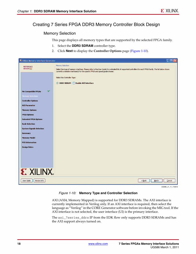
Memory Selection
This page displays all memory types that are supported by the selected FPGA family.
1. Select the DDR3 SDRAM controller type.
2. Click Next to display the Controller Options page (Figure 1-10).
AXI (AXI4, Memory Mapped) is supported for DDR3 SDRAMs. The AXI interface is currently implemented in Verilog only. If an AXI interface is required, then select the language as “Verilog” in the CORE Generator software before invoking the MIG tool. If the AXI interface is not selected, the user interface (UI) is the primary interface.
The axi_7series_ddrx IP from the EDK flow only supports DDR3 SDRAMs and has the AXI support always turned on.
X-Ref Target - Figure 1-10
Figure 1-10: Memory Type and Controller Selection
UG586_c1_11_110610
7 Series FPGAs Memory Interface Solutions www.xilinx.com 19UG586 March 1, 2011
Getting Started with the CORE Generator Software
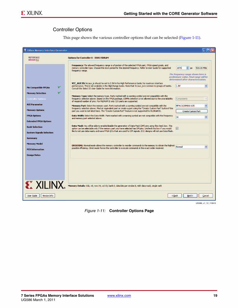
Controller Options
This page shows the various controller options that can be selected (Figure 1-11).X-Ref Target - Figure 1-11
Figure 1-11: Controller Options Page
UG586_c1_12_110610
20 www.xilinx.com 7 Series FPGAs Memory Interface SolutionsUG586 March 1, 2011
Chapter 1: DDR3 SDRAM Memory Interface Solution
If the design has multiple controllers, the controller options page is repeated for each of the controllers. This page is partitioned into a maximum of nine sections. The number of partitions depends on the type of memory selected. The controller options page also contains these pull-down menus to modify different features of the design:
• Frequency: This feature indicates the operating frequency for all the controllers. The frequency block is limited by factors such as the selected FPGA and device speed grade. In the EDK flow, an extra check box (selected by default) allows the user to specify that the frequency information should be calculated automatically from EDK.
• Vccaux_io: Vccaux_io is set based on the period/frequency setting. 2.0V is required at the highest frequency settings in the High Performance column. The MIG tool automatically selects 2.0V when required. Either 1.8 or 2.0V can be used at lower frequencies. Groups of banks share the Vccaux_io supply. See the 7 Series FPGAs SelectIO Resources User Guide [Ref 1] and the 7 Series FPGA Packaging and Pinout Specifications for more information.
• Memory Type: This feature selects the type of memory parts used in the design.
• Memory Part: This option selects a memory part for the design. Selections can be made from the list, or a new part can be created.
• Data Width: The data width value can be selected here based on the memory type selected earlier. The list shows all supported data widths for the selected part. One of the data widths can be selected. These values are generally multiples of the individual device data widths. In some cases, the width might not be an exact multiple. For example, 16 bits is the default data width for x16 components, but 8 bits is also a valid value.
• Data Mask: This option allocates data mask pins when selected. This option should be deselected to deallocate data mask pins and increase pin efficiency. This option is disabled for memory parts that do not support data mask.
• Ordering: This feature allows the memory controller to reorder commands to improve the memory bus efficiency.
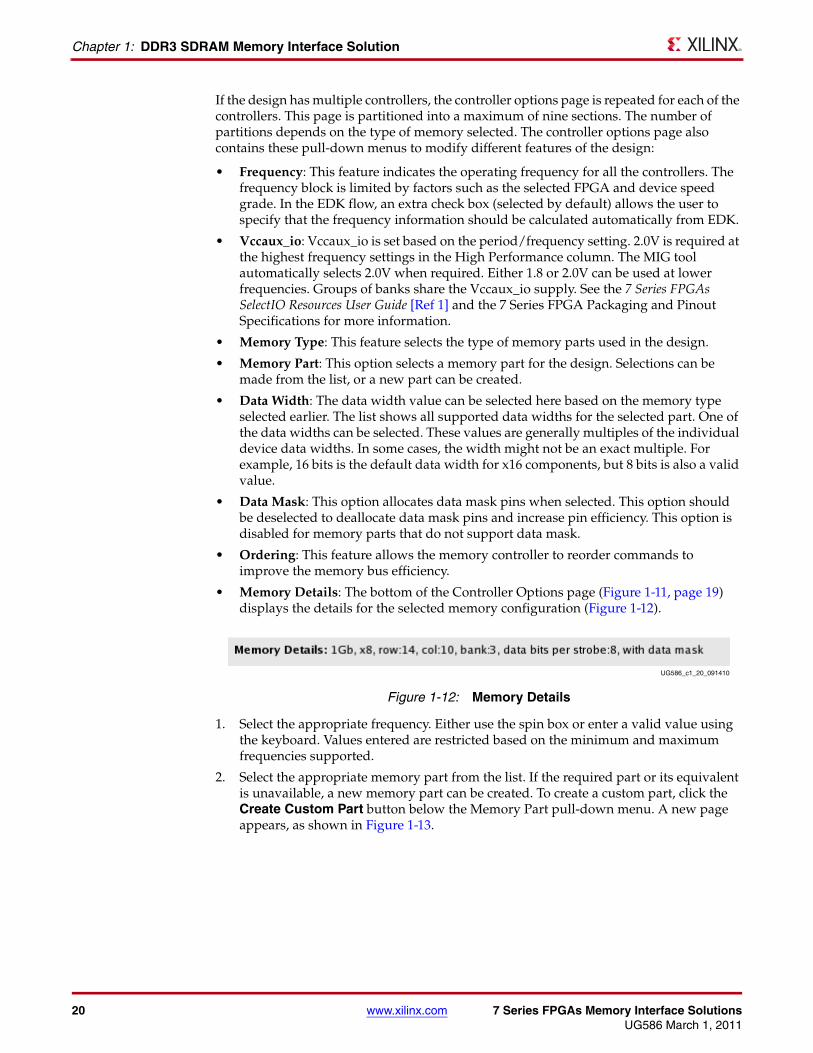
• Memory Details: The bottom of the Controller Options page (Figure 1-11, page 19) displays the details for the selected memory configuration (Figure 1-12).
1. Select the appropriate frequency. Either use the spin box or enter a valid value using the keyboard. Values entered are restricted based on the minimum and maximum frequencies supported.
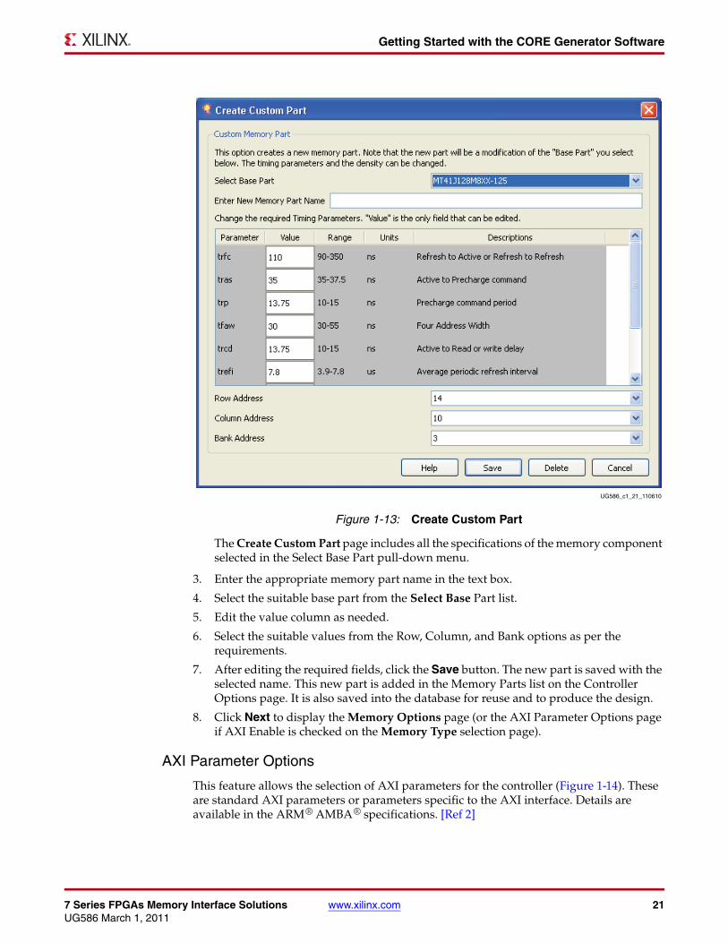
2. Select the appropriate memory part from the list. If the required part or its equivalent is unavailable, a new memory part can be created. To create a custom part, click the Create Custom Part button below the Memory Part pull-down menu. A new page appears, as shown in Figure 1-13.
X-Ref Target - Figure 1-12
Figure 1-12: Memory Details
UG586_c1_20_091410
7 Series FPGAs Memory Interface Solutions www.xilinx.com 21UG586 March 1, 2011
Getting Started with the CORE Generator Software
The Create Custom Part page includes all the specifications of the memory component selected in the Select Base Part pull-down menu.
3. Enter the appropriate memory part name in the text box.
4. Select the suitable base part from the Select Base Part list.
5. Edit the value column as needed.
6. Select the suitable values from the Row, Column, and Bank options as per the requirements.
7. After editing the required fields, click the Save button. The new part is saved with the selected name. This new part is added in the Memory Parts list on the Controller Options page. It is also saved into the database for reuse and to produce the design.
8. Click Next to display the Memory Options page (or the AXI Parameter Options page if AXI Enable is checked on the Memory Type selection page).
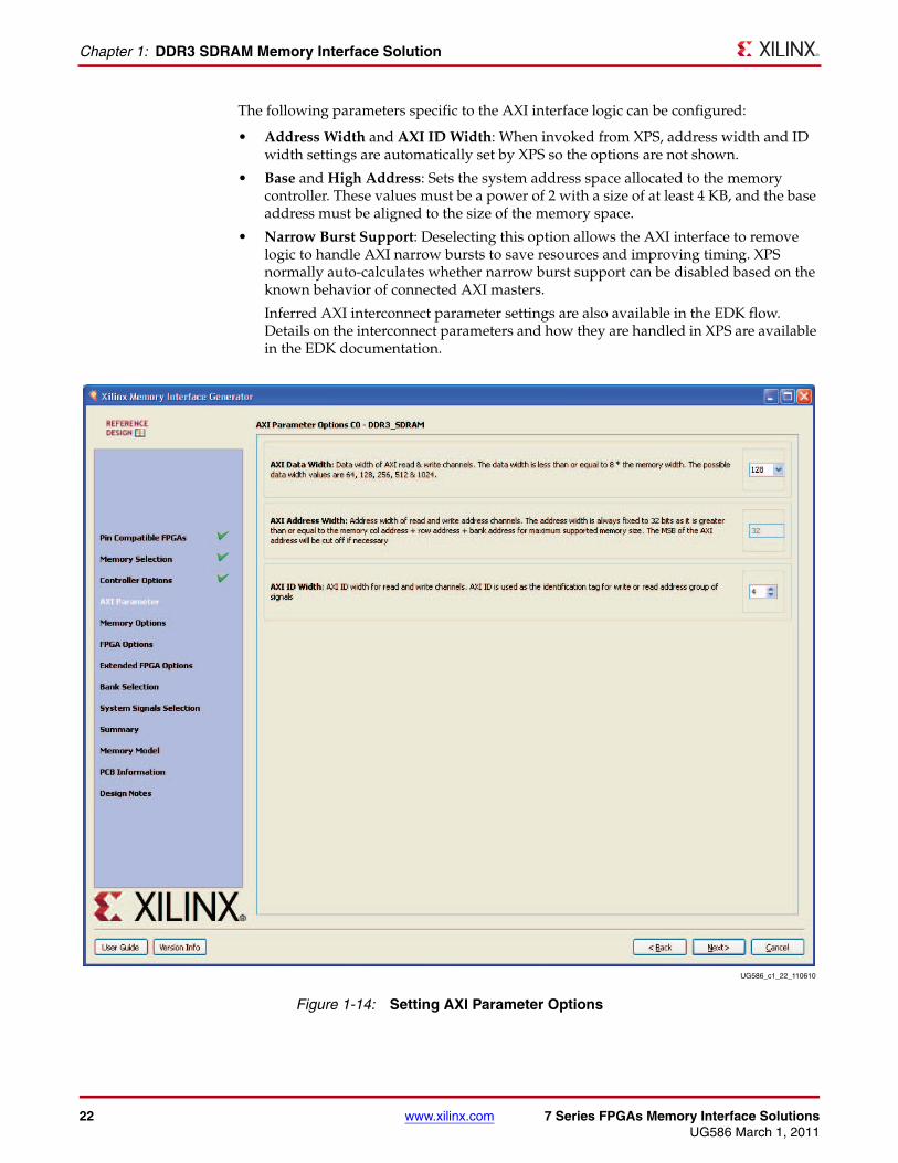
AXI Parameter Options
This feature allows the selection of AXI parameters for the controller (Figure 1-14). These are standard AXI parameters or parameters specific to the AXI interface. Details are available in the ARM® AMBA® specifications. [Ref 2]
X-Ref Target - Figure 1-13
Figure 1-13: Create Custom Part
UG586_c1_21_110610
22 www.xilinx.com 7 Series FPGAs Memory Interface SolutionsUG586 March 1, 2011
Chapter 1: DDR3 SDRAM Memory Interface Solution
The following parameters specific to the AXI interface logic can be configured:
• Address Width and AXI ID Width: When invoked from XPS, address width and ID width settings are automatically set by XPS so the options are not shown.
• Base and High Address: Sets the system address space allocated to the memory controller. These values must be a power of 2 with a size of at least 4 KB, and the base address must be aligned to the size of the memory space.
• Narrow Burst Support: Deselecting this option allows the AXI interface to remove logic to handle AXI narrow bursts to save resources and improving timing. XPS normally auto-calculates whether narrow burst support can be disabled based on the known behavior of connected AXI masters.
Inferred AXI interconnect parameter settings are also available in the EDK flow. Details on the interconnect parameters and how they are handled in XPS are available in the EDK documentation.
X-Ref Target - Figure 1-14
Figure 1-14: Setting AXI Parameter Options
UG586_c1_22_110610
7 Series FPGAs Memory Interface Solutions www.xilinx.com 23UG586 March 1, 2011
Getting Started with the CORE Generator Software
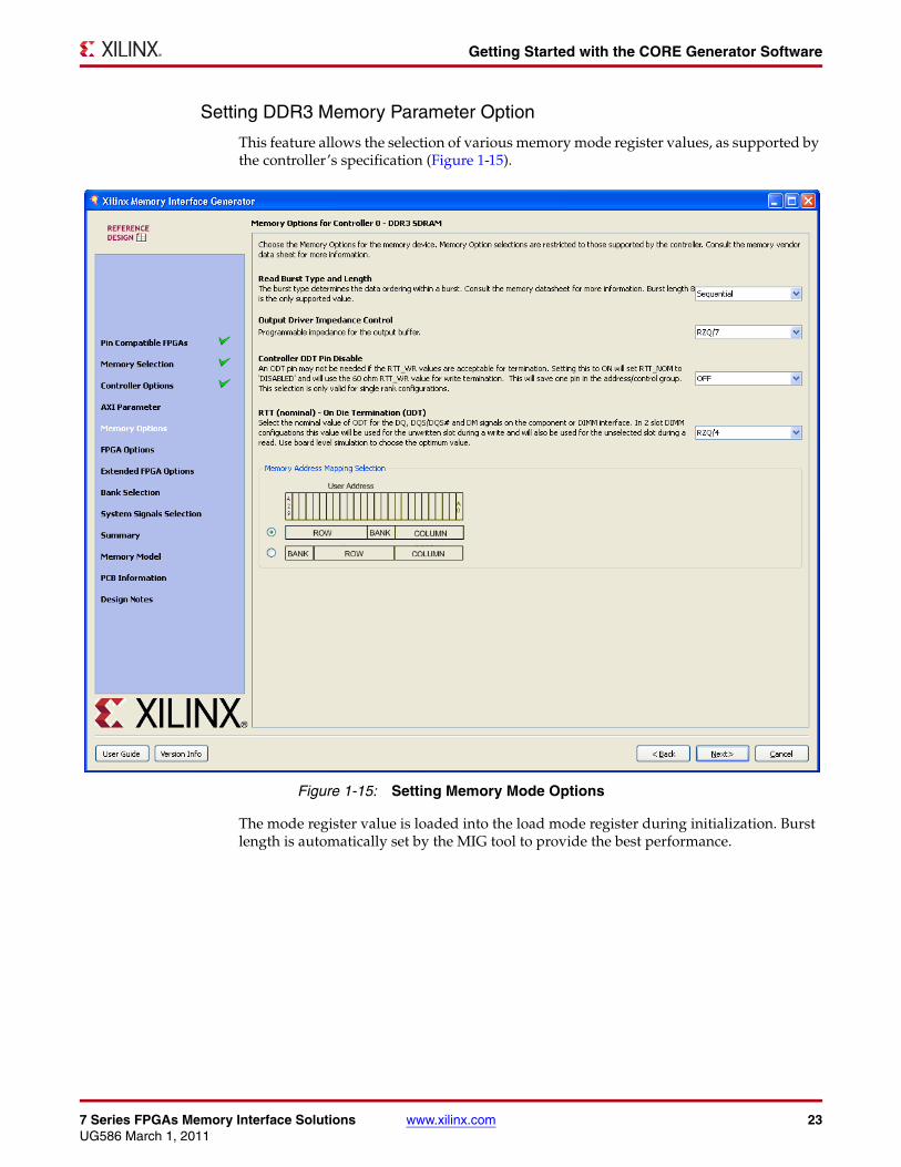
Setting DDR3 Memory Parameter Option
This feature allows the selection of various memory mode register values, as supported by the controller’s specification (Figure 1-15).
The mode register value is loaded into the load mode register during initialization. Burst length is automatically set by the MIG tool to provide the best performance.
X-Ref Target - Figure 1-15
Figure 1-15: Setting Memory Mode Options
24 www.xilinx.com 7 Series FPGAs Memory Interface SolutionsUG586 March 1, 2011
Chapter 1: DDR3 SDRAM Memory Interface Solution
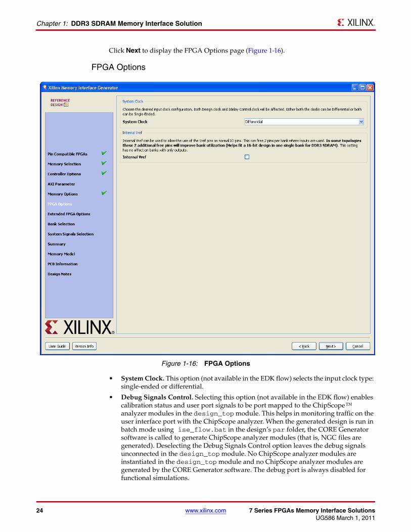
Click Next to display the FPGA Options page (Figure 1-16).
FPGA Options
• System Clock. This option (not available in the EDK flow) selects the input clock type: single-ended or differential.
• Debug Signals Control. Selecting this option (not available in the EDK flow) enables calibration status and user port signals to be port mapped to the ChipScope™ analyzer modules in the design_top module. This helps in monitoring traffic on the user interface port with the ChipScope analyzer. When the generated design is run in batch mode using ise_flow.bat in the design’s par folder, the CORE Generator software is called to generate ChipScope analyzer modules (that is, NGC files are generated). Deselecting the Debug Signals Control option leaves the debug signals unconnected in the design_top module. No ChipScope analyzer modules are instantiated in the design_top module and no ChipScope analyzer modules are generated by the CORE Generator software. The debug port is always disabled for functional simulations.
X-Ref Target - Figure 1-16
Figure 1-16: FPGA Options
7 Series FPGAs Memory Interface Solutions www.xilinx.com 25UG586 March 1, 2011
Getting Started with the CORE Generator Software
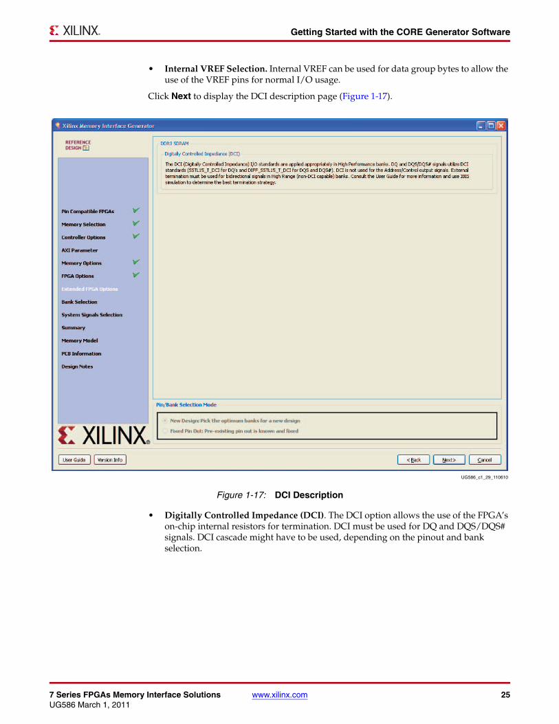
• Internal VREF Selection. Internal VREF can be used for data group bytes to allow the use of the VREF pins for normal I/O usage.
Click Next to display the DCI description page (Figure 1-17).
• Digitally Controlled Impedance (DCI). The DCI option allows the use of the FPGA’s on-chip internal resistors for termination. DCI must be used for DQ and DQS/DQS# signals. DCI cascade might have to be used, depending on the pinout and bank selection.
X-Ref Target - Figure 1-17
Figure 1-17: DCI Description
UG586_c1_29_110610
26 www.xilinx.com 7 Series FPGAs Memory Interface SolutionsUG586 March 1, 2011
Chapter 1: DDR3 SDRAM Memory Interface Solution
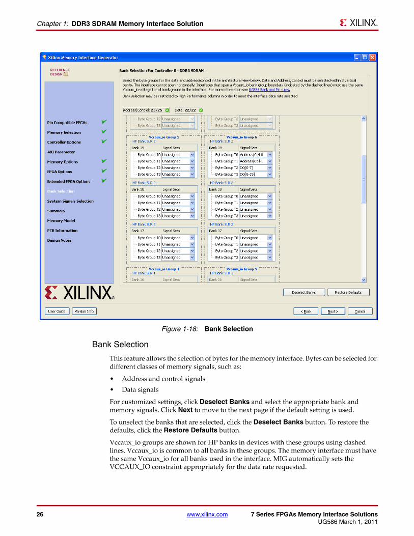
Bank Selection
This feature allows the selection of bytes for the memory interface. Bytes can be selected for different classes of memory signals, such as:
• Address and control signals
• Data signals
For customized settings, click Deselect Banks and select the appropriate bank and memory signals. Click Next to move to the next page if the default setting is used.
To unselect the banks that are selected, click the Deselect Banks button. To restore the defaults, click the Restore Defaults button.
Vccaux_io groups are shown for HP banks in devices with these groups using dashed lines. Vccaux_io is common to all banks in these groups. The memory interface must have the same Vccaux_io for all banks used in the interface. MIG automatically sets the VCCAUX_IO constraint appropriately for the data rate requested.
X-Ref Target - Figure 1-18
Figure 1-18: Bank Selection
7 Series FPGAs Memory Interface Solutions www.xilinx.com 27UG586 March 1, 2011
Getting Started with the CORE Generator Software
Super Logic Regions are indicated by a number in the header in each bank in devices with these regions. For example, "SLR 1". Interfaces cannot span across Super Logic Regions. Not all devices have Super Logic Regions.
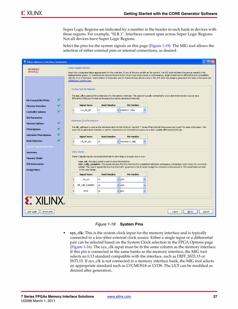
Select the pins for the system signals on this page (Figure 1-19). The MIG tool allows the selection of either external pins or internal connections, as desired.
• sys_clk: This is the system clock input for the memory interface and is typically connected to a low-jitter external clock source. Either a single input or a differential pair can be selected based on the System Clock selection in the FPGA Options page (Figure 1-16). The sys_clk input must be in the same column as the memory interface. If this pin is connected in the same banks as the memory interface, the MIG tool selects an I/O standard compatible with the interface, such as DIFF_SSTL15 or SSTL15. If sys_clk is not connected in a memory interface bank, the MIG tool selects an appropriate standard such as LVCMOS18 or LVDS. The UCF can be modified as desired after generation.
X-Ref Target - Figure 1-19
Figure 1-19: System Pins
28 www.xilinx.com 7 Series FPGAs Memory Interface SolutionsUG586 March 1, 2011
Chapter 1: DDR3 SDRAM Memory Interface Solution
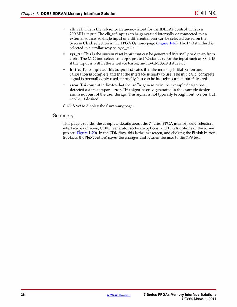
• clk_ref: This is the reference frequency input for the IDELAY control. This is a 200 MHz input. The clk_ref input can be generated internally or connected to an external source. A single input or a differential pair can be selected based on the System Clock selection in the FPGA Options page (Figure 1-16). The I/O standard is selected in a similar way as sys_clk.
• sys_rst: This is the system reset input that can be generated internally or driven from a pin. The MIG tool selects an appropriate I/O standard for the input such as SSTL15 if the input is within the interface banks, and LVCMOS18 if it is not.
• init_calib_complete: This output indicates that the memory initialization and calibration is complete and that the interface is ready to use. The init_calib_complete signal is normally only used internally, but can be brought out to a pin if desired.
• error: This output indicates that the traffic generator in the example design has detected a data compare error. This signal is only generated in the example design and is not part of the user design. This signal is not typically brought out to a pin but can be, if desired.
Click Next to display the Summary page.
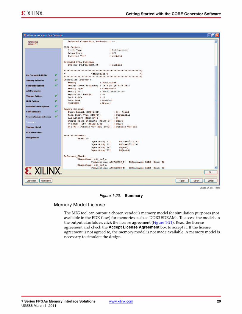
Summary
This page provides the complete details about the 7 series FPGA memory core selection, interface parameters, CORE Generator software options, and FPGA options of the active project (Figure 1-20). In the EDK flow, this is the last screen, and clicking the Finish button (replaces the Next button) saves the changes and returns the user to the XPS tool.
7 Series FPGAs Memory Interface Solutions www.xilinx.com 29UG586 March 1, 2011
Getting Started with the CORE Generator Software
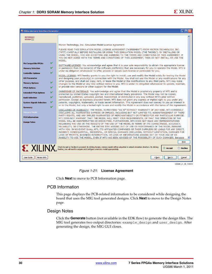
Memory Model License
The MIG tool can output a chosen vendor’s memory model for simulation purposes (not available in the EDK flow) for memories such as DDR3 SDRAMs. To access the models in the output sim folder, click the license agreement (Figure 1-21). Read the license agreement and check the Accept License Agreement box to accept it. If the license agreement is not agreed to, the memory model is not made available. A memory model is necessary to simulate the design.
X-Ref Target - Figure 1-20
Figure 1-20: Summary
UG586_c1_38_110610
30 www.xilinx.com 7 Series FPGAs Memory Interface SolutionsUG586 March 1, 2011
Chapter 1: DDR3 SDRAM Memory Interface Solution
Click Next to move to PCB Information page.
PCB Information
This page displays the PCB-related information to be considered while designing the board that uses the MIG tool generated designs. Click Next to move to the Design Notes page.
Design Notes
Click the Generate button (not available in the EDK flow) to generate the design files. The MIG tool generates two output directories: example_design and user_design. After generating the design, the MIG GUI closes.
X-Ref Target - Figure 1-21
Figure 1-21: License Agreement
UG586_c1_39_110610
7 Series FPGAs Memory Interface Solutions www.xilinx.com 31UG586 March 1, 2011
Getting Started with the CORE Generator Software
Directory Structure and File Descriptions
Overview
Output Directory Structure
The MIG tool outputs (non-EDK flow) are generated with folder name <component name>.
Note: In the EDK flow, the MIG project file is stored in <EDK Project Directory>/data/<Instance Name>_mig_saved.prj and should be retained with the XPS project. The MIG UCF with pin location information is written to <EDK Project Directory>/__xps/<Instance Name>/mig.ucf and is translated to an EDK core-level UCF at <EDK Project Directory>/implementation/<Instance Name>_wrapper/<Instance Name>.ucf during builds.
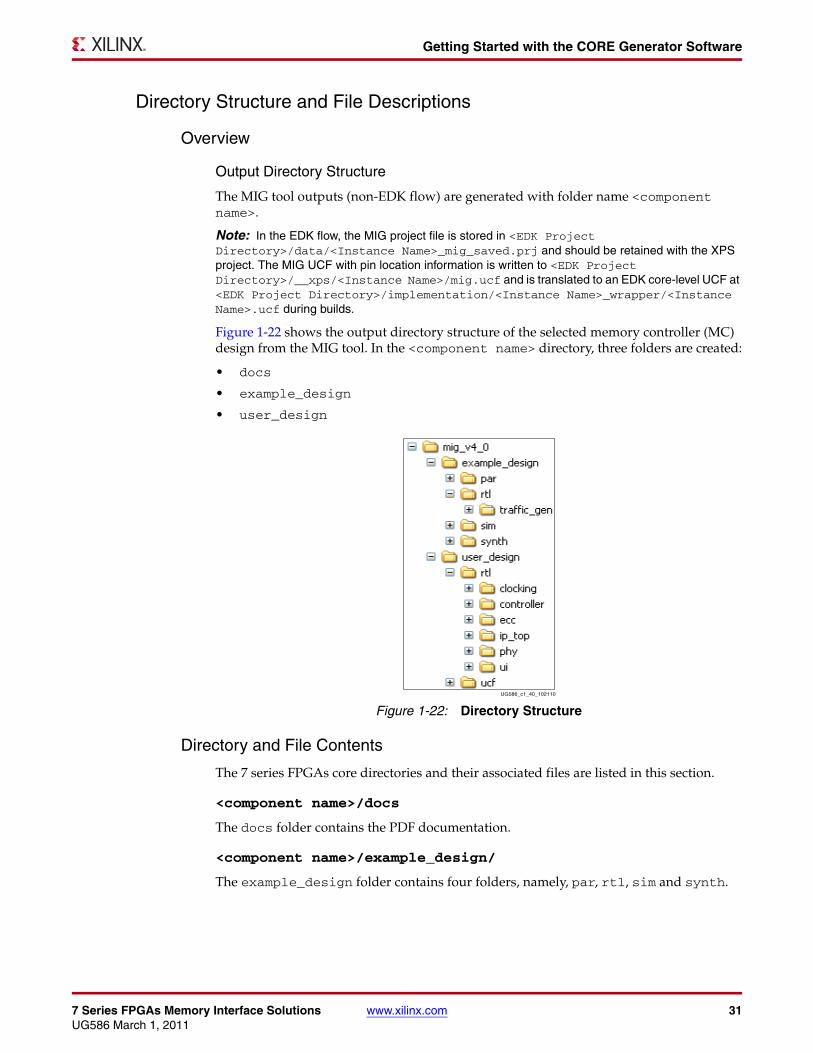
Figure 1-22 shows the output directory structure of the selected memory controller (MC) design from the MIG tool. In the <component name> directory, three folders are created:
• docs
• example_design
• user_design
Directory and File Contents
The 7 series FPGAs core directories and their associated files are listed in this section.
<component name>/docs
The docs folder contains the PDF documentation.
<component name>/example_design/
The example_design folder contains four folders, namely, par, rtl, sim and synth.
X-Ref Target - Figure 1-22
Figure 1-22: Directory StructureUG586_c1_40_102110
32 www.xilinx.com 7 Series FPGAs Memory Interface SolutionsUG586 March 1, 2011
Chapter 1: DDR3 SDRAM Memory Interface Solution
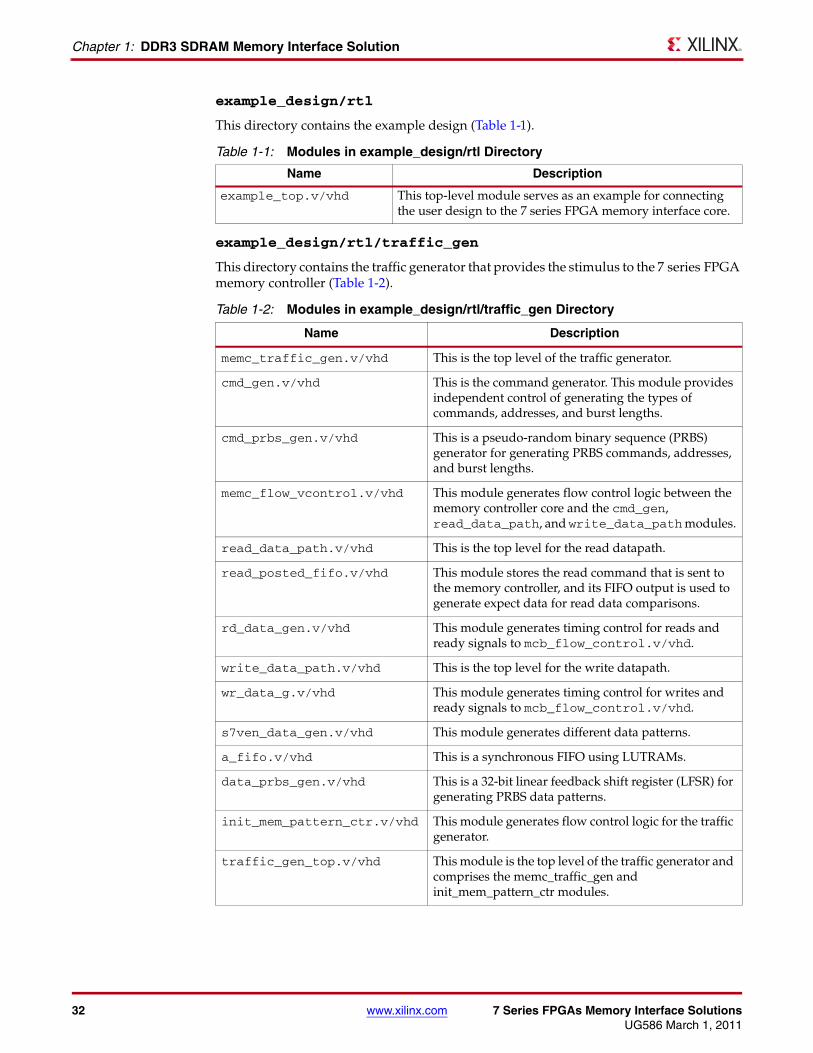
example_design/rtl
This directory contains the example design (Table 1-1).
example_design/rtl/traffic_gen
This directory contains the traffic generator that provides the stimulus to the 7 series FPGA memory controller (Table 1-2).
Table 1-1: Modules in example_design/rtl Directory
Name Description
example_top.v/vhd This top-level module serves as an example for connecting the user design to the 7 series FPGA memory interface core.
Table 1-2: Modules in example_design/rtl/traffic_gen Directory
Name Description
memc_traffic_gen.v/vhd This is the top level of the traffic generator.
cmd_gen.v/vhd This is the command generator. This module provides independent control of generating the types of commands, addresses, and burst lengths.
cmd_prbs_gen.v/vhd This is a pseudo-random binary sequence (PRBS) generator for generating PRBS commands, addresses, and burst lengths.
memc_flow_vcontrol.v/vhd This module generates flow control logic between the memory controller core and the cmd_gen, read_data_path, and write_data_path modules.
read_data_path.v/vhd This is the top level for the read datapath.
read_posted_fifo.v/vhd This module stores the read command that is sent to the memory controller, and its FIFO output is used to generate expect data for read data comparisons.
rd_data_gen.v/vhd This module generates timing control for reads and ready signals to mcb_flow_control.v/vhd.
write_data_path.v/vhd This is the top level for the write datapath.
wr_data_g.v/vhd This module generates timing control for writes and ready signals to mcb_flow_control.v/vhd.
s7ven_data_gen.v/vhd This module generates different data patterns.
a_fifo.v/vhd This is a synchronous FIFO using LUTRAMs.
data_prbs_gen.v/vhd This is a 32-bit linear feedback shift register (LFSR) for generating PRBS data patterns.
init_mem_pattern_ctr.v/vhd This module generates flow control logic for the traffic generator.
traffic_gen_top.v/vhd This module is the top level of the traffic generator and comprises the memc_traffic_gen and init_mem_pattern_ctr modules.
7 Series FPGAs Memory Interface Solutions www.xilinx.com 33UG586 March 1, 2011
Getting Started with the CORE Generator Software
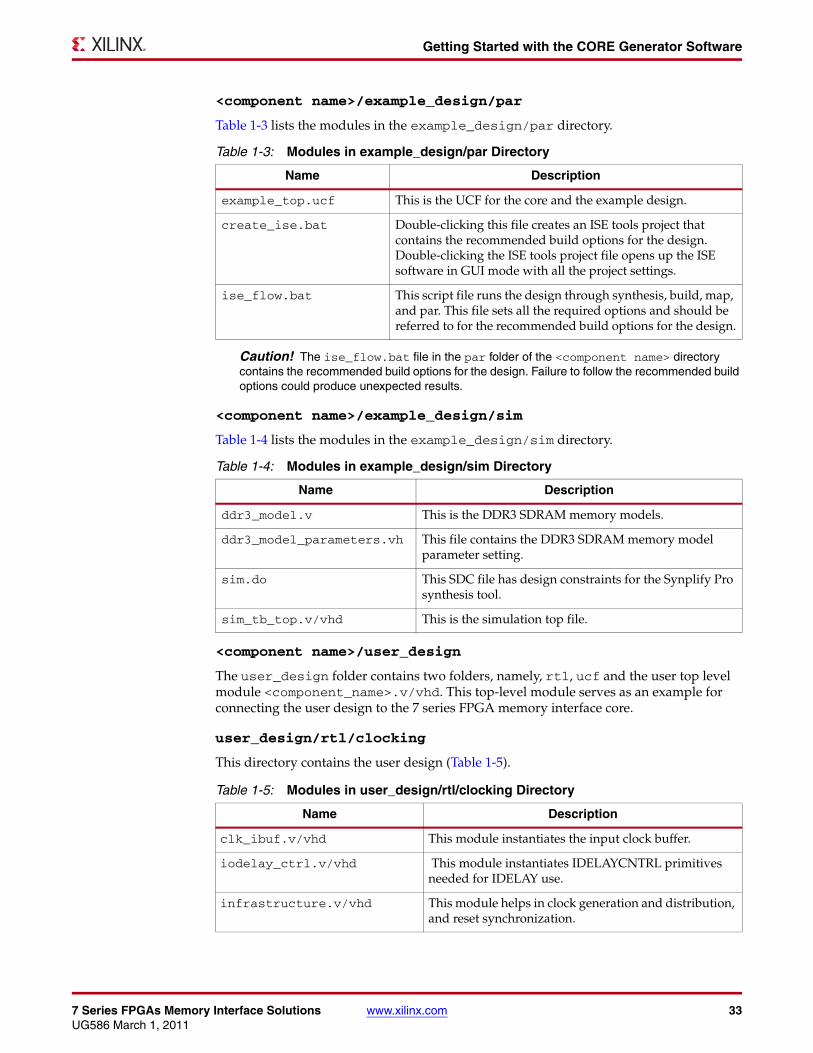
<component name>/example_design/par
Table 1-3 lists the modules in the example_design/par directory.
Caution! The ise_flow.bat file in the par folder of the <component name> directory contains the recommended build options for the design. Failure to follow the recommended build options could produce unexpected results.
<component name>/example_design/sim
Table 1-4 lists the modules in the example_design/sim directory.
<component name>/user_design
The user_design folder contains two folders, namely, rtl, ucf and the user top level module <component_name>.v/vhd. This top-level module serves as an example for connecting the user design to the 7 series FPGA memory interface core.
user_design/rtl/clocking
This directory contains the user design (Table 1-5).
Table 1-3: Modules in example_design/par Directory
Name Description
example_top.ucf This is the UCF for the core and the example design.
create_ise.bat Double-clicking this file creates an ISE tools project that contains the recommended build options for the design. Double-clicking the ISE tools project file opens up the ISE software in GUI mode with all the project settings.
ise_flow.bat This script file runs the design through synthesis, build, map, and par. This file sets all the required options and should be referred to for the recommended build options for the design.
Table 1-4: Modules in example_design/sim Directory
Name Description
ddr3_model.v This is the DDR3 SDRAM memory models.
ddr3_model_parameters.vh This file contains the DDR3 SDRAM memory model parameter setting.
sim.do This SDC file has design constraints for the Synplify Pro synthesis tool.
sim_tb_top.v/vhd This is the simulation top file.
Table 1-5: Modules in user_design/rtl/clocking Directory
Name Description
clk_ibuf.v/vhd This module instantiates the input clock buffer.
iodelay_ctrl.v/vhd This module instantiates IDELAYCNTRL primitives needed for IDELAY use.
infrastructure.v/vhd This module helps in clock generation and distribution, and reset synchronization.
34 www.xilinx.com 7 Series FPGAs Memory Interface SolutionsUG586 March 1, 2011
Chapter 1: DDR3 SDRAM Memory Interface Solution
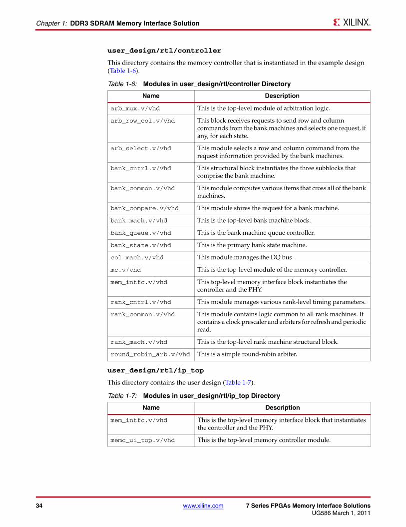
user_design/rtl/controller
This directory contains the memory controller that is instantiated in the example design (Table 1-6).
user_design/rtl/ip_top
This directory contains the user design (Table 1-7).
Table 1-6: Modules in user_design/rtl/controller Directory
Name Description
arb_mux.v/vhd This is the top-level module of arbitration logic.
arb_row_col.v/vhd This block receives requests to send row and column commands from the bank machines and selects one request, if any, for each state.
arb_select.v/vhd This module selects a row and column command from the request information provided by the bank machines.
bank_cntrl.v/vhd This structural block instantiates the three subblocks that comprise the bank machine.
bank_common.v/vhd This module computes various items that cross all of the bank machines.
bank_compare.v/vhd This module stores the request for a bank machine.
bank_mach.v/vhd This is the top-level bank machine block.
bank_queue.v/vhd This is the bank machine queue controller.
bank_state.v/vhd This is the primary bank state machine.
col_mach.v/vhd This module manages the DQ bus.
mc.v/vhd This is the top-level module of the memory controller.
mem_intfc.v/vhd This top-level memory interface block instantiates the controller and the PHY.
rank_cntrl.v/vhd This module manages various rank-level timing parameters.
rank_common.v/vhd This module contains logic common to all rank machines. It contains a clock prescaler and arbiters for refresh and periodic read.
rank_mach.v/vhd This is the top-level rank machine structural block.
round_robin_arb.v/vhd This is a simple round-robin arbiter.
Table 1-7: Modules in user_design/rtl/ip_top Directory
Name Description
mem_intfc.v/vhd This is the top-level memory interface block that instantiates the controller and the PHY.
memc_ui_top.v/vhd This is the top-level memory controller module.
7 Series FPGAs Memory Interface Solutions www.xilinx.com 35UG586 March 1, 2011
Getting Started with the CORE Generator Software
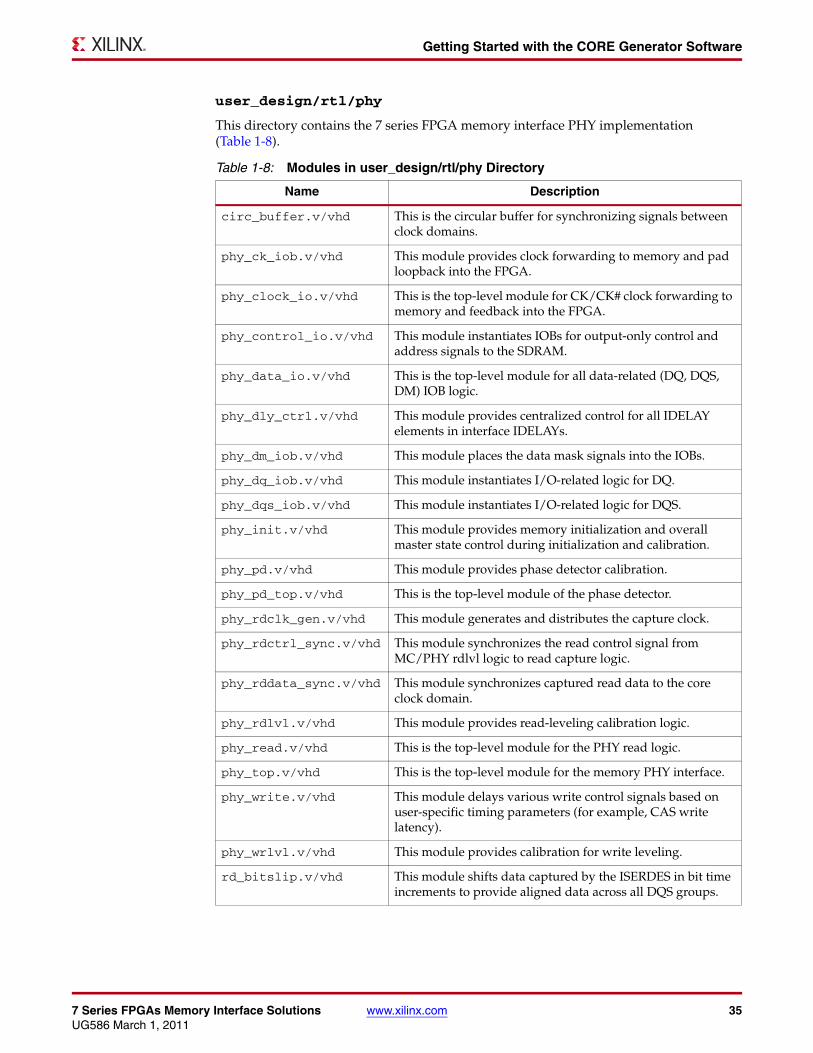
user_design/rtl/phy
This directory contains the 7 series FPGA memory interface PHY implementation (Table 1-8).
Table 1-8: Modules in user_design/rtl/phy Directory
Name Description
circ_buffer.v/vhd This is the circular buffer for synchronizing signals between clock domains.
phy_ck_iob.v/vhd This module provides clock forwarding to memory and pad loopback into the FPGA.
phy_clock_io.v/vhd This is the top-level module for CK/CK# clock forwarding to memory and feedback into the FPGA.
phy_control_io.v/vhd This module instantiates IOBs for output-only control and address signals to the SDRAM.
phy_data_io.v/vhd This is the top-level module for all data-related (DQ, DQS, DM) IOB logic.
phy_dly_ctrl.v/vhd This module provides centralized control for all IDELAY elements in interface IDELAYs.
phy_dm_iob.v/vhd This module places the data mask signals into the IOBs.
phy_dq_iob.v/vhd This module instantiates I/O-related logic for DQ.
phy_dqs_iob.v/vhd This module instantiates I/O-related logic for DQS.
phy_init.v/vhd This module provides memory initialization and overall master state control during initialization and calibration.
phy_pd.v/vhd This module provides phase detector calibration.
phy_pd_top.v/vhd This is the top-level module of the phase detector.
phy_rdclk_gen.v/vhd This module generates and distributes the capture clock.
phy_rdctrl_sync.v/vhd This module synchronizes the read control signal from MC/PHY rdlvl logic to read capture logic.
phy_rddata_sync.v/vhd This module synchronizes captured read data to the core clock domain.
phy_rdlvl.v/vhd This module provides read-leveling calibration logic.
phy_read.v/vhd This is the top-level module for the PHY read logic.
phy_top.v/vhd This is the top-level module for the memory PHY interface.
phy_write.v/vhd This module delays various write control signals based on user-specific timing parameters (for example, CAS write latency).
phy_wrlvl.v/vhd This module provides calibration for write leveling.
rd_bitslip.v/vhd This module shifts data captured by the ISERDES in bit time increments to provide aligned data across all DQS groups.
36 www.xilinx.com 7 Series FPGAs Memory Interface SolutionsUG586 March 1, 2011
Chapter 1: DDR3 SDRAM Memory Interface Solution
user_design/rtl/ui
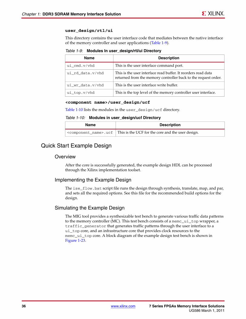
This directory contains the user interface code that mediates between the native interface of the memory controller and user applications (Table 1-9).
<component name>/user_design/ucf
Table 1-10 lists the modules in the user_design/ucf directory.
Quick Start Example Design
Overview
After the core is successfully generated, the example design HDL can be processed through the Xilinx implementation toolset.
Implementing the Example Design
The ise_flow.bat script file runs the design through synthesis, translate, map, and par, and sets all the required options. See this file for the recommended build options for the design.
Simulating the Example Design
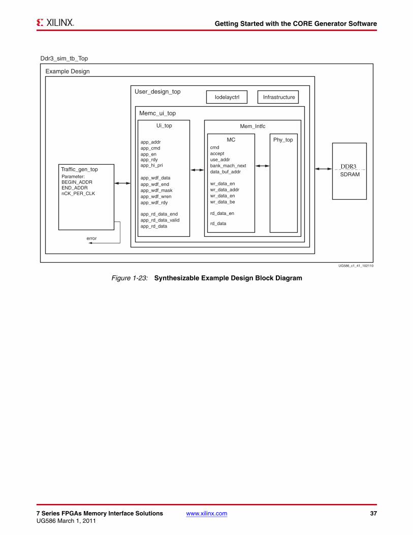
The MIG tool provides a synthesizable test bench to generate various traffic data patterns to the memory controller (MC). This test bench consists of a memc_ui_top wrapper, a traffic_generator that generates traffic patterns through the user interface to a ui_top core, and an infrastructure core that provides clock resources to the memc_ui_top core. A block diagram of the example design test bench is shown in Figure 1-23.
Table 1-9: Modules In user_design/rtl/ui Directory
Name Description
ui_cmd.v/vhd This is the user interface command port.
ui_rd_data.v/vhd This is the user interface read buffer. It reorders read data returned from the memory controller back to the request order.
ui_wr_data.v/vhd This is the user interface write buffer.
ui_top.v/vhd This is the top level of the memory controller user interface.
Table 1-10: Modules in user_design/ucf Directory
Name Description
<component_name>.ucf This is the UCF for the core and the user design.
7 Series FPGAs Memory Interface Solutions www.xilinx.com 37UG586 March 1, 2011
Getting Started with the CORE Generator Software
X-Ref Target - Figure 1-23
Figure 1-23: Synthesizable Example Design Block Diagram
UG586_c1_41_102110
Ddr3_sim_tb_Top
Example Design
Ui_top
app_addrapp_cmdapp_en
app_hi_pri
app_wdf_dataapp_wdf_endapp_wdf_maskapp_wdf_wren
app_rd_data
app_rd_data_endapp_rd_data_valid
app_wdf_rdy
Mem_Intfc
DDR2/DDR3SDRAM
Traffic_gen_top
Memc_ui_top
MCcmdacceptuse_addrbank_mach_nextdata_buf_addr
wr_data_enwr_data_addrwr_data_enwr_data_be
rd_data_en
rd_data
Phy_top
error
Parameter:BEGIN_ADDREND_ADDRnCK_PER_CLK
Iodelayctrl Infrastructure
app_rdy
User_design_top
DDR3
38 www.xilinx.com 7 Series FPGAs Memory Interface SolutionsUG586 March 1, 2011
Chapter 1: DDR3 SDRAM Memory Interface Solution
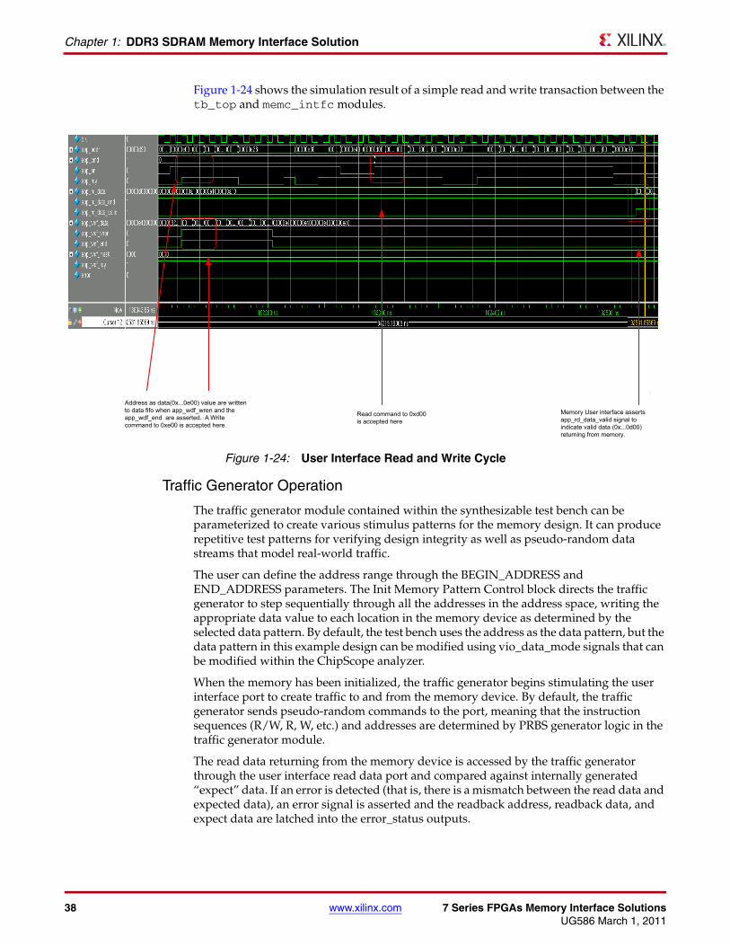
Figure 1-24 shows the simulation result of a simple read and write transaction between the tb_top and memc_intfc modules.
Traffic Generator Operation
The traffic generator module contained within the synthesizable test bench can be parameterized to create various stimulus patterns for the memory design. It can produce repetitive test patterns for verifying design integrity as well as pseudo-random data streams that model real-world traffic.
The user can define the address range through the BEGIN_ADDRESS and END_ADDRESS parameters. The Init Memory Pattern Control block directs the traffic generator to step sequentially through all the addresses in the address space, writing the appropriate data value to each location in the memory device as determined by the selected data pattern. By default, the test bench uses the address as the data pattern, but the data pattern in this example design can be modified using vio_data_mode signals that can be modified within the ChipScope analyzer.
When the memory has been initialized, the traffic generator begins stimulating the user interface port to create traffic to and from the memory device. By default, the traffic generator sends pseudo-random commands to the port, meaning that the instruction sequences (R/W, R, W, etc.) and addresses are determined by PRBS generator logic in the traffic generator module.
The read data returning from the memory device is accessed by the traffic generator through the user interface read data port and compared against internally generated “expect” data. If an error is detected (that is, there is a mismatch between the read data and expected data), an error signal is asserted and the readback address, readback data, and expect data are latched into the error_status outputs.
X-Ref Target - Figure 1-24
Figure 1-24: User Interface Read and Write Cycle
�������������� ��������������������
���������������������������������������������������������������������������� ��������������������������
����������������� ������������������� ������������������� ������� ��� �������������� ������������������������!�������������� ���������������������
7 Series FPGAs Memory Interface Solutions www.xilinx.com 39UG586 March 1, 2011
Getting Started with the CORE Generator Software
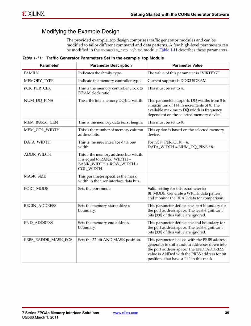
Modifying the Example DesignThe provided example_top design comprises traffic generator modules and can be modified to tailor different command and data patterns. A few high-level parameters can be modified in the example_top.v/vhd module. Table 1-11 describes these parameters.
Table 1-11: Traffic Generator Parameters Set in the example_top Module
Parameter Parameter Description Parameter Value
FAMILY Indicates the family type. The value of this parameter is “VIRTEX7”.
MEMORY_TYPE Indicate the memory controller type. Current support is DDR3 SDRAM.
nCK_PER_CLK This is the memory controller clock to DRAM clock ratio.
This must be set to 4.
NUM_DQ_PINS The is the total memory DQ bus width. This parameter supports DQ widths from 8 to a maximum of 144 in increments of 8. The available maximum DQ width is frequency dependent on the selected memory device.
MEM_BURST_LEN This is the memory data burst length. This must be set to 8.
MEM_COL_WIDTH This is the number of memory column address bits.
This option is based on the selected memory device.
DATA_WIDTH This is the user interface data bus width.
For nCK_PER_CLK = 4, DATA_WIDTH = NUM_DQ_PINS * 8.
ADDR_WIDTH This is the memory address bus width. It is equal to RANK_WIDTH + BANK_WIDTH + ROW_WIDTH + COL_WIDTH.
MASK_SIZE This parameter specifies the mask width in the user interface data bus.
PORT_MODE Sets the port mode. Valid setting for this parameter is: BI_MODE: Generate a WRITE data pattern and monitor the READ data for comparison.
BEGIN_ADDRESS Sets the memory start address boundary.
This parameter defines the start boundary for the port address space. The least-significant bits [3:0] of this value are ignored.
END_ADDRESS Sets the memory end address boundary.
This parameter defines the end boundary for the port address space. The least-significant bits [3:0] of this value are ignored.
PRBS_EADDR_MASK_POS Sets the 32-bit AND MASK position. This parameter is used with the PRBS address generator to shift random addresses down into the port address space. The END_ADDRESS value is ANDed with the PRBS address for bit positions that have a “1” in this mask.
40 www.xilinx.com 7 Series FPGAs Memory Interface SolutionsUG586 March 1, 2011
Chapter 1: DDR3 SDRAM Memory Interface Solution
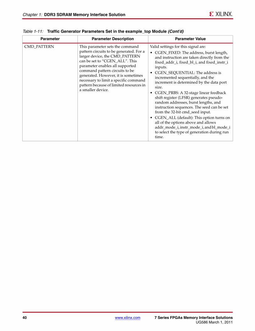
CMD_PATTERN This parameter sets the command pattern circuits to be generated. For a larger device, the CMD_PATTERN can be set to “CGEN_ALL”. This parameter enables all supported command pattern circuits to be generated. However, it is sometimes necessary to limit a specific command pattern because of limited resources in a smaller device.
Valid settings for this signal are:
• CGEN_FIXED: The address, burst length, and instruction are taken directly from the fixed_addr_i, fixed_bl_i, and fixed_instr_i inputs.
• CGEN_SEQUENTIAL: The address is incremented sequentially, and the increment is determined by the data port size.
• CGEN_PRBS: A 32-stage linear feedback shift register (LFSR) generates pseudo-random addresses, burst lengths, and instruction sequences. The seed can be set from the 32-bit cmd_seed input.
• CGEN_ALL (default): This option turns on all of the options above and allows addr_mode_i, instr_mode_i, and bl_mode_i to select the type of generation during run time.
Table 1-11: Traffic Generator Parameters Set in the example_top Module (Cont’d)
Parameter Parameter Description Parameter Value
7 Series FPGAs Memory Interface Solutions www.xilinx.com 41UG586 March 1, 2011
Getting Started with the CORE Generator Software
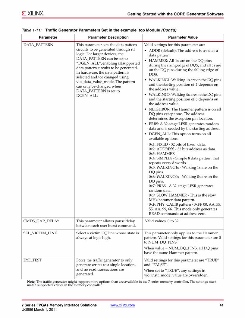
DATA_PATTERN This parameter sets the data pattern circuits to be generated through rtl logic. For larger devices, the DATA_PATTERN can be set to “DGEN_ALL”, enabling all supported data pattern circuits to be generated. In hardware, the data pattern is selected and/or changed using vio_data_value_mode. The pattern can only be changed when DATA_PATTERN is set to DGEN_ALL.
Valid settings for this parameter are:
• ADDR (default): The address is used as a data pattern.
• HAMMER: All 1s are on the DQ pins during the rising edge of DQS, and all 0s are on the DQ pins during the falling edge of DQS.
• WALKING1: Walking 1s are on the DQ pins and the starting position of 1 depends on the address value.
• WALKING0: Walking 0s are on the DQ pins and the starting position of 0 depends on the address value.
• NEIGHBOR: The Hammer pattern is on all DQ pins except one. The address determines the exception pin location.
• PRBS: A 32-stage LFSR generates random data and is seeded by the starting address.
• DGEN_ALL: This option turns on all available options:
0x1: FIXED - 32 bits of fixed_data.0x2: ADDRESS - 32 bits address as data.0x3: HAMMER 0x4: SIMPLE8 - Simple 8 data pattern that repeats every 8 words.0x5: WALKING1s - Walking 1s are on the DQ pins. 0x6: WALKING0s - Walking 0s are on the DQ pins. 0x7: PRBS - A 32-stage LFSR generates random data. 0x9: SLOW HAMMER - This is the slow MHz hammer data pattern.0xF: PHY_CALIB pattern - 0xFF, 00, AA, 55, 55, AA, 99, 66. This mode only generates READ commands at address zero.
CMDS_GAP_DELAY This parameter allows pause delay between each user burst command.
Valid values: 0 to 32.
SEL_VICTIM_LINE Select a victim DQ line whose state is always at logic high.
This parameter only applies to the Hammer pattern. Valid settings for this parameter are 0 to NUM_DQ_PINS.
When value = NUM_DQ_PINS, all DQ pins have the same Hammer pattern.
EYE_TEST Force the traffic generator to only generate writes to a single location, and no read transactions are generated.
Valid settings for this parameter are “TRUE” and “FALSE”.
When set to “TRUE”, any settings in vio_instr_mode_value are overridden.
Note: The traffic generator might support more options than are available in the 7 series memory controller. The settings must match supported values in the memory controller.
Table 1-11: Traffic Generator Parameters Set in the example_top Module (Cont’d)
Parameter Parameter Description Parameter Value
42 www.xilinx.com 7 Series FPGAs Memory Interface SolutionsUG586 March 1, 2011
Chapter 1: DDR3 SDRAM Memory Interface Solution
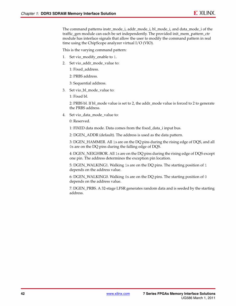
The command patterns instr_mode_i, addr_mode_i, bl_mode_i, and data_mode_i of the traffic_gen module can each be set independently. The provided init_mem_pattern_ctr module has interface signals that allow the user to modify the command pattern in real time using the ChipScope analyzer virtual I/O (VIO).
This is the varying command pattern:
1. Set vio_modify_enable to 1.
2. Set vio_addr_mode_value to:
1: Fixed_address.
2: PRBS address.
3: Sequential address.
3. Set vio_bl_mode_value to:
1: Fixed bl.
2: PRBS bl. If bl_mode value is set to 2, the addr_mode value is forced to 2 to generate the PRBS address.
4. Set vio_data_mode_value to:
0: Reserved.
1: FIXED data mode. Data comes from the fixed_data_i input bus.
2: DGEN_ADDR (default). The address is used as the data pattern.
3: DGEN_HAMMER. All 1s are on the DQ pins during the rising edge of DQS, and all 0s are on the DQ pins during the falling edge of DQS.
4: DGEN_NEIGHBOR. All 1s are on the DQ pins during the rising edge of DQS except one pin. The address determines the exception pin location.
5: DGEN_WALKING1. Walking 1s are on the DQ pins. The starting position of 1 depends on the address value.
6: DGEN_WALKING0. Walking 0s are on the DQ pins. The starting position of 0 depends on the address value.
7: DGEN_PRBS. A 32-stage LFSR generates random data and is seeded by the starting address.
7 Series FPGAs Memory Interface Solutions www.xilinx.com 43UG586 March 1, 2011
Getting Started with the CORE Generator Software
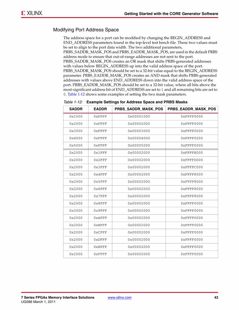
Modifying Port Address Space
The address space for a port can be modified by changing the BEGIN_ADDRESS and END_ADDRESS parameters found in the top-level test bench file. These two values must be set to align to the port data width. The two additional parameters, PRBS_SADDR_MASK_POS and PRBS_EADDR_MASK_POS, are used in the default PRBS address mode to ensure that out-of-range addresses are not sent to the port. PRBS_SADDR_MASK_POS creates an OR mask that shifts PRBS-generated addresses with values below BEGIN_ADDRESS up into the valid address space of the port. PRBS_SADDR_MASK_POS should be set to a 32-bit value equal to the BEGIN_ADDRESS parameter. PRBS_EADDR_MASK_POS creates an AND mask that shifts PRBS-generated addresses with values above END_ADDRESS down into the valid address space of the port. PRBS_EADDR_MASK_POS should be set to a 32-bit value, where all bits above the most-significant address bit of END_ADDRESS are set to 1 and all remaining bits are set to 0. Table 1-12 shows some examples of setting the two mask parameters.
Table 1-12: Example Settings for Address Space and PRBS Masks
SADDR EADDR PRBS_SADDR_MASK_POS PRBS_EADDR_MASK_POS
0x1000 0xFFFF 0x00001000 0xFFFF0000
0x2000 0xFFFF 0x00002000 0xFFFF0000
0x3000 0xFFFF 0x00003000 0xFFFF0000
0x4000 0xFFFF 0x00004000 0xFFFF0000
0x5000 0xFFFF 0x00005000 0xFFFF0000
0x2000 0x1FFF 0x00002000 0xFFFFE000
0x2000 0x2FFF 0x00002000 0xFFFFD000
0x2000 0x3FFF 0x00002000 0xFFFFC000
0x2000 0x4FFF 0x00002000 0xFFFF8000
0x2000 0x5FFF 0x00002000 0xFFFF8000
0x2000 0x6FFF 0x00002000 0xFFFF8000
0x2000 0x7FFF 0x00002000 0xFFFF8000
0x2000 0x8FFF 0x00002000 0xFFFF0000
0x2000 0x9FFF 0x00002000 0xFFFF0000
0x2000 0xAFFF 0x00002000 0xFFFF0000
0x2000 0xBFFF 0x00002000 0xFFFF0000
0x2000 0xCFFF 0x00002000 0xFFFF0000
0x2000 0xDFFF 0x00002000 0xFFFF0000
0x2000 0xEFFF 0x00002000 0xFFFF0000
0x2000 0xFFFF 0x00002000 0xFFFF0000
44 www.xilinx.com 7 Series FPGAs Memory Interface SolutionsUG586 March 1, 2011
Chapter 1: DDR3 SDRAM Memory Interface Solution
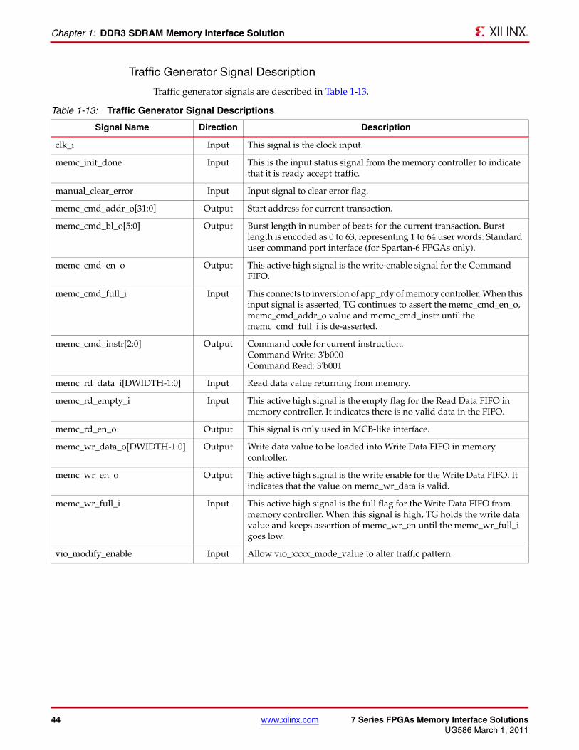
Traffic Generator Signal Description
Traffic generator signals are described in Table 1-13.
Table 1-13: Traffic Generator Signal Descriptions
Signal Name Direction Description
clk_i Input This signal is the clock input.
memc_init_done Input This is the input status signal from the memory controller to indicate that it is ready accept traffic.
manual_clear_error Input Input signal to clear error flag.
memc_cmd_addr_o[31:0] Output Start address for current transaction.
memc_cmd_bl_o[5:0] Output Burst length in number of beats for the current transaction. Burst length is encoded as 0 to 63, representing 1 to 64 user words. Standard user command port interface (for Spartan-6 FPGAs only).
memc_cmd_en_o Output This active high signal is the write-enable signal for the Command FIFO.
memc_cmd_full_i Input This connects to inversion of app_rdy of memory controller. When this input signal is asserted, TG continues to assert the memc_cmd_en_o, memc_cmd_addr_o value and memc_cmd_instr until the memc_cmd_full_i is de-asserted.
memc_cmd_instr[2:0] Output Command code for current instruction. Command Write: 3'b000Command Read: 3'b001
memc_rd_data_i[DWIDTH-1:0] Input Read data value returning from memory.
memc_rd_empty_i Input This active high signal is the empty flag for the Read Data FIFO in memory controller. It indicates there is no valid data in the FIFO.
memc_rd_en_o Output This signal is only used in MCB-like interface.
memc_wr_data_o[DWIDTH-1:0] Output Write data value to be loaded into Write Data FIFO in memory controller.
memc_wr_en_o Output This active high signal is the write enable for the Write Data FIFO. It indicates that the value on memc_wr_data is valid.
memc_wr_full_i Input This active high signal is the full flag for the Write Data FIFO from memory controller. When this signal is high, TG holds the write data value and keeps assertion of memc_wr_en until the memc_wr_full_i goes low.
vio_modify_enable Input Allow vio_xxxx_mode_value to alter traffic pattern.
7 Series FPGAs Memory Interface Solutions www.xilinx.com 45UG586 March 1, 2011
Getting Started with the CORE Generator Software
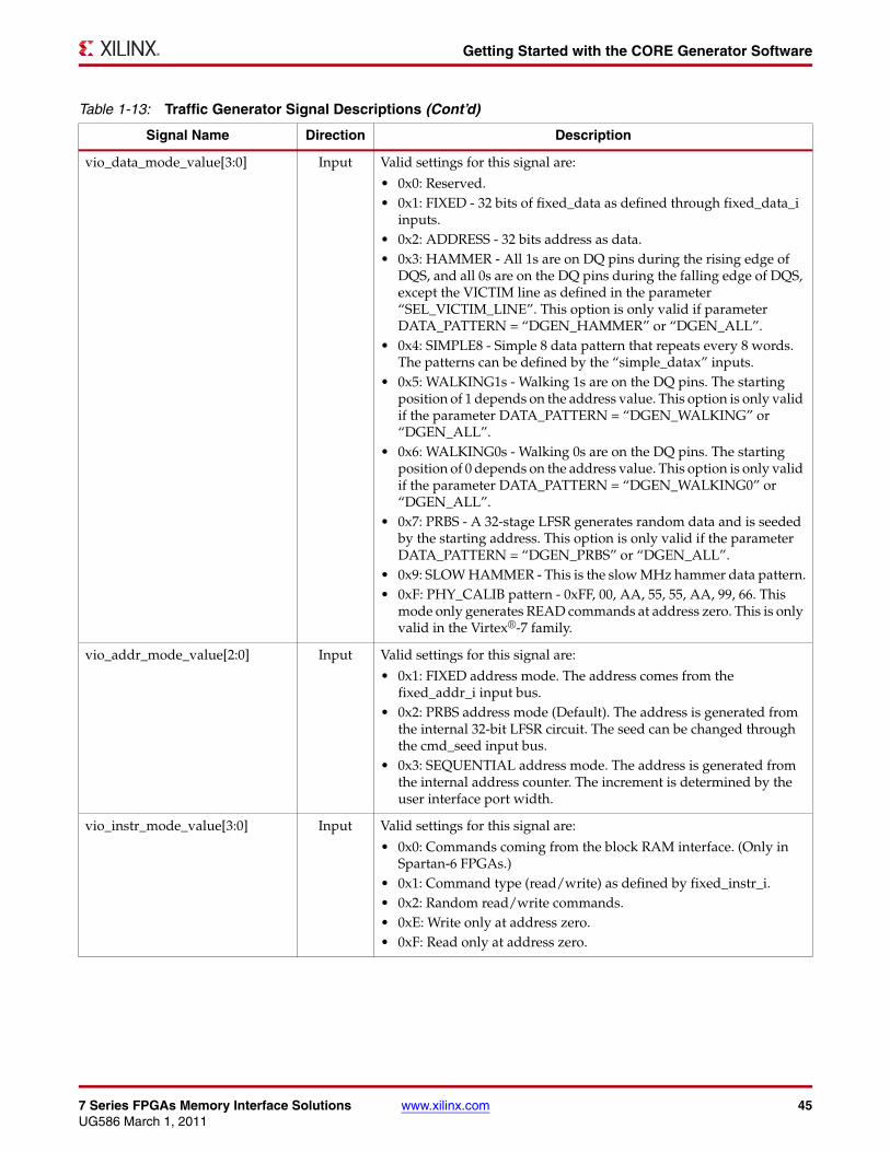
vio_data_mode_value[3:0] Input Valid settings for this signal are:
• 0x0: Reserved.• 0x1: FIXED - 32 bits of fixed_data as defined through fixed_data_i
inputs.• 0x2: ADDRESS - 32 bits address as data.• 0x3: HAMMER - All 1s are on DQ pins during the rising edge of
DQS, and all 0s are on the DQ pins during the falling edge of DQS, except the VICTIM line as defined in the parameter “SEL_VICTIM_LINE”. This option is only valid if parameter DATA_PATTERN = “DGEN_HAMMER” or “DGEN_ALL”.
• 0x4: SIMPLE8 - Simple 8 data pattern that repeats every 8 words. The patterns can be defined by the “simple_datax” inputs.
• 0x5: WALKING1s - Walking 1s are on the DQ pins. The starting position of 1 depends on the address value. This option is only valid if the parameter DATA_PATTERN = “DGEN_WALKING” or “DGEN_ALL”.
• 0x6: WALKING0s - Walking 0s are on the DQ pins. The starting position of 0 depends on the address value. This option is only valid if the parameter DATA_PATTERN = “DGEN_WALKING0” or “DGEN_ALL”.
• 0x7: PRBS - A 32-stage LFSR generates random data and is seeded by the starting address. This option is only valid if the parameter DATA_PATTERN = “DGEN_PRBS” or “DGEN_ALL”.
• 0x9: SLOW HAMMER - This is the slow MHz hammer data pattern.• 0xF: PHY_CALIB pattern - 0xFF, 00, AA, 55, 55, AA, 99, 66. This
mode only generates READ commands at address zero. This is only valid in the Virtex®-7 family.
vio_addr_mode_value[2:0] Input Valid settings for this signal are:
• 0x1: FIXED address mode. The address comes from the fixed_addr_i input bus.
• 0x2: PRBS address mode (Default). The address is generated from the internal 32-bit LFSR circuit. The seed can be changed through the cmd_seed input bus.
• 0x3: SEQUENTIAL address mode. The address is generated from the internal address counter. The increment is determined by the user interface port width.
vio_instr_mode_value[3:0] Input Valid settings for this signal are:
• 0x0: Commands coming from the block RAM interface. (Only in Spartan-6 FPGAs.)
• 0x1: Command type (read/write) as defined by fixed_instr_i.• 0x2: Random read/write commands.• 0xE: Write only at address zero.• 0xF: Read only at address zero.
Table 1-13: Traffic Generator Signal Descriptions (Cont’d)
Signal Name Direction Description
46 www.xilinx.com 7 Series FPGAs Memory Interface SolutionsUG586 March 1, 2011
Chapter 1: DDR3 SDRAM Memory Interface Solution
Memory Initialization and Traffic Test Flow
After power up, the Init Memory Control block directs the traffic generator to initialize the memory with the selected data pattern through the memory initialization procedure.
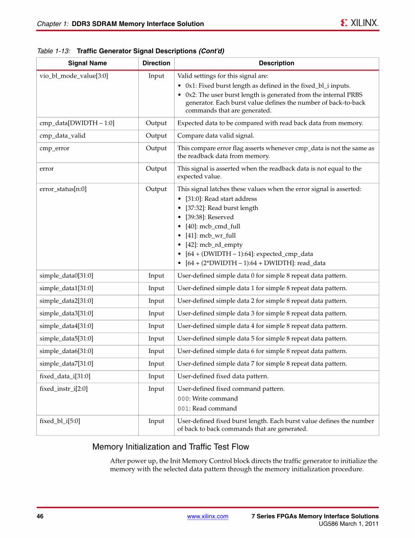
vio_bl_mode_value[3:0] Input Valid settings for this signal are:
• 0x1: Fixed burst length as defined in the fixed_bl_i inputs.• 0x2: The user burst length is generated from the internal PRBS
generator. Each burst value defines the number of back-to-back commands that are generated.
cmp_data[DWIDTH – 1:0] Output Expected data to be compared with read back data from memory.
cmp_data_valid Output Compare data valid signal.
cmp_error Output This compare error flag asserts whenever cmp_data is not the same as the readback data from memory.
error Output This signal is asserted when the readback data is not equal to the expected value.
error_status[n:0] Output This signal latches these values when the error signal is asserted:
• [31:0]: Read start address• [37:32]: Read burst length• [39:38]: Reserved• [40]: mcb_cmd_full• [41]: mcb_wr_full• [42]: mcb_rd_empty• [64 + (DWIDTH – 1):64]: expected_cmp_data• [64 + (2*DWIDTH – 1):64 + DWIDTH]: read_data
simple_data0[31:0] Input User-defined simple data 0 for simple 8 repeat data pattern.
simple_data1[31:0] Input User-defined simple data 1 for simple 8 repeat data pattern.
simple_data2[31:0] Input User-defined simple data 2 for simple 8 repeat data pattern.
simple_data3[31:0] Input User-defined simple data 3 for simple 8 repeat data pattern.
simple_data4[31:0] Input User-defined simple data 4 for simple 8 repeat data pattern.
simple_data5[31:0] Input User-defined simple data 5 for simple 8 repeat data pattern.
simple_data6[31:0] Input User-defined simple data 6 for simple 8 repeat data pattern.
simple_data7[31:0] Input User-defined simple data 7 for simple 8 repeat data pattern.
fixed_data_i[31:0] Input User-defined fixed data pattern.
fixed_instr_i[2:0] Input User-defined fixed command pattern.
000: Write command
001: Read command
fixed_bl_i[5:0] Input User-defined fixed burst length. Each burst value defines the number of back to back commands that are generated.
Table 1-13: Traffic Generator Signal Descriptions (Cont’d)
Signal Name Direction Description
7 Series FPGAs Memory Interface Solutions www.xilinx.com 47UG586 March 1, 2011
Getting Started with the CORE Generator Software
Memory Initialization
1. The data_mode_i input is set to select the data pattern (for example, data_mode_i[3:0] = 0010 for the address as the data pattern).
2. The start_addr_i input is set to define the lower address boundary.
3. The end_addr_i input is set to define the upper address boundary.
4. bl_mode_i is set to 01 to get the burst length from the fixed_bl_i input.
5. The fixed_bl_i input is set to either 16 or 32.
6. instr_mode_i is set to 0001 to get the instruction from the fixed_instr_i input.
7. The fixed_instr_i input is set to the “WR” command value of the memory device.
8. addr_mode_i is set to 11 for the sequential address mode to fill up the memory space.
9. mode_load_i is asserted for one clock cycle.
When the memory space is initialized with the selected data pattern, the Init Memory Control block instructs the traffic generator to begin running traffic through the traffic test flow procedure (by default, the addr_mode_i, instr_mode_i, and bl_mode_i inputs are set to select PRBS mode).
Traffic Test Flow
1. The addr_mode_i input is set to the desired mode (PRBS is the default).
2. The cmd_seed_i and data_seed_i input values are set for the internal PRBS generator. This step is not required for other patterns.
3. The instr_mode_i input is set to the desired mode (PRBS is the default).
4. The bl_mode_i input is set to the desired mode (PRBS is the default).
5. The data_mode_i input should have the same value as in the memory pattern initialization stage detailed in Memory Initialization.
6. The run_traffic_i input is asserted to start running traffic.
7. If an error occurs during testing (for example, the read data does not match the expected data), the error bit is set until reset is applied.
8. Upon receiving an error, the error_status bus latches the values defined in Table 1-13, page 44.
With some modifications, the example design can be changed to allow addr_mode_i, instr_mode_i, and bl_mode_i to be changed dynamically when run_traffic_i is deasserted. However, after changing the setting, the memory initialization steps need to be repeated to ensure that the proper pattern is loaded into the memory space.
Setting up for Simulation
The Xilinx UniSim library must be mapped into the simulator. The test bench provided with the example design supports these pre-implementation simulations:
• The test bench, along with vendor’s memory model used in the example design
• The RTL files of the memory controller and the PHY core, created by the MIG tool
To run the simulation, go to this directory:
<project_dir>/<example_design>/sim
ModelSim is the only supported simulation tool. The simple test bench can be run using ModelSim by executing the sim.do script.
48 www.xilinx.com 7 Series FPGAs Memory Interface SolutionsUG586 March 1, 2011
Chapter 1: DDR3 SDRAM Memory Interface Solution
Getting Started with EDKEDK provides an alternative package to the RTL created by the MIG tool in the CORE Generator software. The IP catalog in XPS contains the IP core axi_7series_ddrx with the same RTL that is provided by the MIG tool. The difference is that the RTL is packaged as an EDK pcore suitable for use in embedded processor based systems. The axi_7series_ddrx pcore only provides an AXI4 slave interface to DDR3 SDRAM in Verilog.
The simplest way to get started with the axi_7series_ddrx memory controller is to use the base system builder (BSB) wizard in XPS. The BSB guides the user through a series of options to provide an entire embedded project with an optional axi_7series_ddrx memory controller. If the memory controller is selected, an already configured, connected, and tested axi_7series_ddrx controller is provided for a particular reference board such as the ML605 board. For more information on BSB, see chapter 2 of EDK Concepts, Tools, and Techniques. [Ref 4]
When starting with a new project, the axi_7series_ddrx IP can be added to the design by dragging the memory controller into the project from the IP catalog. The axi_7series_ddrx IP is configured using the same MIG tool used in the CORE Generator software and therefore the GUI flow is as described in Getting Started with the CORE Generator Software, page 9. However, instead of generating the RTL top-level wrappers with the parameters already set, the MIG tool sets the parameters for the RTL in the XPS MHS file and in a MIG .prj file. From the parameters in the MHS along with the MIG .prj file, the pcore is able to generate the correct constraints and parameter values for itself during the XPS Platform Generator (PlatGen) tool. Because the pcore is only a component in the system, the clock/reset structure must also be configured in XPS and is not automatically generated, as in the RTL in the CORE Generator tool. After the IP is configured and the ports are connected, XPS is used to perform all other aspects of IP management, including generating a bitstream and running simulations. In general, parameters described in this document for the memory controller can be converted to the EDK syntax. This requires all parameters to be upper case and prefixed with “C_.” For more information about EDK and XPS, see EDK Concepts, Tools, and Techniques [Ref 4] and the Embedded System Tools Reference Manual. [Ref 5]
Core ArchitectureThis section describes the architecture of the 7 series FPGAs memory interface solutions core, providing an overview of the core modules and interfaces.
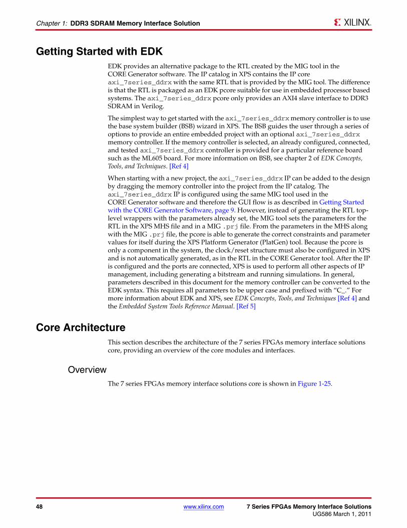
OverviewThe 7 series FPGAs memory interface solutions core is shown in Figure 1-25.
7 Series FPGAs Memory Interface Solutions www.xilinx.com 49UG586 March 1, 2011
Core Architecture
User Design
The user design block shown in Figure 1-25 is any FPGA design that requires to be connected to an external DDR3 SDRAM. The user design connects to the memory controller via the user interface. An example user design is provided with the core.
AXI4 Slave Interface Block
The AXI4 slave interface maps AXI4 transactions to the UI to provide an industry-standard bus protocol interface to the memory controller.
User Interface Block and User Interface
The UI block presents the UI to the user design block. It provides a simple alternative to the native interface by presenting a flat address space and buffering read and write data.
Memory Controller and Native Interface
The front end of the memory controller (MC) presents the native interface to the UI block. The native interface allows the user design to submit memory read and write requests and provides the mechanism to move data from the user design to the external memory device, and vice versa. The back end of the memory controller connects to the physical interface and handles all the interface requirements to that module. The memory controller also provides a reordering option that reorders received requests to optimize data throughput and latency.
X-Ref Target - Figure 1-25
Figure 1-25: 7 Series FPGAs Memory Interface Solution
UG586_c1_43_090910
rst
clk
app_addr
app_cmd
app_en
app_hi_pri
app_wdf_data
app_wdf_end
app_wdf_mask
app_wdf_wren
app_rdy
app_rd_data
app_rd_data_end
app_rd_data_valid
app_wdf_rdy
ddr_ad dr
ddr_ba
ddr_cas_n
ddr_ck
ddr_cke
ddr_cs_n
ddr_dm
ddr_o dt
ddr_ra s_n
ddr_reset_n
ddr we n
ddr_dq
ddr_dqs_n
ddr_dqs
UserInterface
Block
MemoryController
PhysicalLayer
UserDesign
DDR2/DDR3SDRAM
IOB
7 Series FPGA Memory Interface SolutionUser Interface
Physical Interface7 Series FPGA
Native Interface MC/PHY Interface
ddr_ck_n
ddr_parity
DDR3
50 www.xilinx.com 7 Series FPGAs Memory Interface SolutionsUG586 March 1, 2011
Chapter 1: DDR3 SDRAM Memory Interface Solution
PHY and the Physical Interface
The front end of the PHY connects to the memory controller. The back end of the PHY connects to the external memory device. The PHY handles all memory device signal sequencing and timing.
IDELAYCTRL
An IDELAYCTRL is required in any bank that uses IDELAYs. IDELAYs are associated with the data group, the capture clocks, and the resynchronization (BUFR-rsync) clocks. Any bank/clock region that uses these signals require an IDELAYCTRL.
The MIG tool instantiates one IODELAYCTRL and then uses the IODELAY_GROUP attribute (see the iodelay_ctrl.v/.vhd module). Based on this attribute, the ISE tool properly replicates IODELAYCTRLs as needed within the design.
The IDELAYCTRL reference frequency should be set to 200 MHz. Based on the IODELAY_GROUP attribute that is set, the ISE tool replicates the IODELAYCTRLs for each region where the IDELAY blocks exist. When a user creates a multi-controller design on their own, each MIG output has the component instantiated with the primitive. This violates the rules for IODELAYCTRLs and the usage of the IODELAY_GRP attribute. IODELAYCTRLs need to have only one instantiation of the component with the attribute set properly, and allow the tools to replicate as needed.
User InterfaceThe UI is shown in Table 1-14 and connects to an FPGA user design to allow access to an external memory device.
Table 1-14: User Interface
Signal Direction Description
app_addr[ADDR_WIDTH – 1:0] Input This input indicates the address for the current request.
app_cmd[2:0] Input This input selects the command for the current request.
app_en Input This is the active high strobe for the app_addr[], app_cmd[2:0], app_sz, and app_hi_pri inputs.
app_rdy Output This output indicates that the UI is ready to accept commands. If the signal is deasserted when app_en is enabled, the current app_cmd and app_addr must be retried until app_rdy is asserted.
app_hi_pri Input This active high input elevates the priority of the current request.
app_rd_data[APP_DATA_WIDTH – 1:0]
Output This provides the output data from read commands.
app_rd_data_end Output This active high output indicates that the current clock cycle is the last cycle of output data on app_rd_data[].
7 Series FPGAs Memory Interface Solutions www.xilinx.com 51UG586 March 1, 2011
Core Architecture
app_addr[ADDR_WIDTH – 1:0]
This input indicates the address for the request currently being submitted to the UI. The UI aggregates all the address fields of the external SDRAM and presents a flat address space to the user.
app_rd_data_valid Output This active high output indicates that app_rd_data[] is valid.
app_sz Input This input is reserved and should be tied to 0.
app_wdf_data[APP_DATA_WIDTH – 1:0]
Input This provides the data for write commands.
app_wdf_end Input This active high input indicates that the current clock cycle is the last cycle of input data on app_wdf_data[].
app_wdf_mask[APP_MASK_WIDTH – 1:0]
Input This provides the mask for app_wdf_data[].
app_wdf_rdy Output This output indicates that the write data FIFO is ready to receive data. Write data is accepted when app_wdf_rdy = 1’b1 and app_wdf_wren = 1’b1.
app_wdf_wren Input This is the active high strobe for app_wdf_data[].
clk Input This UI clock must be a quarter of the DRAM clock.
clk_mem Input This is a full-frequency memory clock.
init_calib_complete Output PHY asserts init_calib_complete when calibration is finished.
app_ecc_multiple_err[7:0](1) Output This signal is applicable when ECC is enabled and is valid along with app_rd_data_valid. The app_ecc_multiple_err[3:0] signal is non-zero if the read data from the external memory has two bit errors per beat of the read burst. The SECDED algorithm does not correct the corresponding read data and puts a non-zero value on this signal to notify the corrupted read data at the UI.
rst Input This is the active high UI reset.
Notes: 1. This signal is brought up to the memc_ui_top module level only. This signal should only be used
when ECC is enabled.
Table 1-14: User Interface (Cont’d)
Signal Direction Description
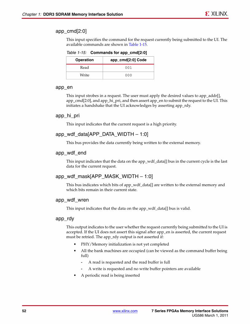
52 www.xilinx.com 7 Series FPGAs Memory Interface SolutionsUG586 March 1, 2011
Chapter 1: DDR3 SDRAM Memory Interface Solution
app_cmd[2:0]
This input specifies the command for the request currently being submitted to the UI. The available commands are shown in Table 1-15.
app_en
This input strobes in a request. The user must apply the desired values to app_addr[], app_cmd[2:0], and app_hi_pri, and then assert app_en to submit the request to the UI. This initiates a handshake that the UI acknowledges by asserting app_rdy.
app_hi_pri
This input indicates that the current request is a high priority.
app_wdf_data[APP_DATA_WIDTH – 1:0]
This bus provides the data currently being written to the external memory.
app_wdf_end
This input indicates that the data on the app_wdf_data[] bus in the current cycle is the last data for the current request.
app_wdf_mask[APP_MASK_WIDTH – 1:0]
This bus indicates which bits of app_wdf_data[] are written to the external memory and which bits remain in their current state.
app_wdf_wren
This input indicates that the data on the app_wdf_data[] bus is valid.
app_rdy
This output indicates to the user whether the request currently being submitted to the UI is accepted. If the UI does not assert this signal after app_en is asserted, the current request must be retried. The app_rdy output is not asserted if:
• PHY/Memory initialization is not yet completed
• All the bank machines are occupied (can be viewed as the command buffer being full)
- A read is requested and the read buffer is full
- A write is requested and no write buffer pointers are available
• A periodic read is being inserted
Table 1-15: Commands for app_cmd[2:0]
Operation app_cmd[2:0] Code
Read 001
Write 000
7 Series FPGAs Memory Interface Solutions www.xilinx.com 53UG586 March 1, 2011
Core Architecture
app_rd_data[APP_DATA_WIDTH – 1:0]
This output contains the data read from the external memory.
app_rd_data_end
This output indicates that the data on the app_rd_data[] bus in the current cycle is the last data for the current request.
app_rd_data_valid
This output indicates that the data on the app_rd_data[] bus is valid.
app_wdf_rdy
This output indicates that the write data FIFO is ready to receive data. Write data is accepted when both app_wdf_rdy ad app_wdf_wren are asserted.
rst
This is the reset input for the UI.
clk
This is the input clock for the UI. It must be a quarter the frequency of the clock going out to the external SDRAM.
clk_mem
This is a full-frequency clock provided from the MMCM and should only be used as an input to the OSERDES.
init_calib_complete
PHY asserts init_calib_complete when calibration is finished. The application has no need to wait for init_calib_complete before sending commands to the memory controller.
AXI4 Slave Interface BlockThe AXI4 slave interface block maps AXI4 transactions to the UI interface to provide an industry-standard bus protocol interface to the memory controller. The AXI4 slave interface is optional in designs provided through the MIG tool. The AXI4 slave interface is required with the axi_7series_ddrx memory controller provided in EDK. The RTL is consistent between both tools. For details on the AXI4 signaling protocol, see the ARM AMBA specifications. [Ref 2]
The overall design is composed of separate blocks to handle each AXI channel, which allows for independent read and write transactions. Read and write commands to the UI rely on a simple round-robin arbiter to handle simultaneous requests. The address read/address write modules are responsible for chopping the AXI4 burst/wrap requests into smaller memory size burst lengths of either four or eight, and also conveying the smaller burst lengths to the read/write data modules so they can interact with the user interface.
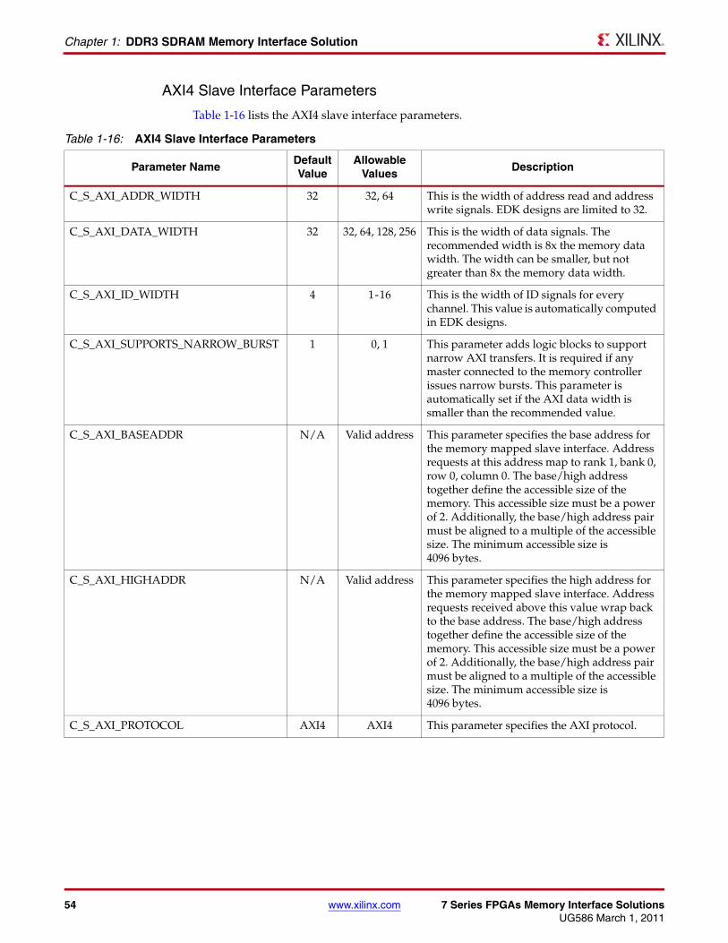
54 www.xilinx.com 7 Series FPGAs Memory Interface SolutionsUG586 March 1, 2011
Chapter 1: DDR3 SDRAM Memory Interface Solution
AXI4 Slave Interface Parameters
Table 1-16 lists the AXI4 slave interface parameters.
Table 1-16: AXI4 Slave Interface Parameters
Parameter NameDefault Value
Allowable Values
Description
C_S_AXI_ADDR_WIDTH 32 32, 64 This is the width of address read and address write signals. EDK designs are limited to 32.
C_S_AXI_DATA_WIDTH 32 32, 64, 128, 256 This is the width of data signals. The recommended width is 8x the memory data width. The width can be smaller, but not greater than 8x the memory data width.
C_S_AXI_ID_WIDTH 4 1-16 This is the width of ID signals for every channel. This value is automatically computed in EDK designs.
C_S_AXI_SUPPORTS_NARROW_BURST 1 0, 1 This parameter adds logic blocks to support narrow AXI transfers. It is required if any master connected to the memory controller issues narrow bursts. This parameter is automatically set if the AXI data width is smaller than the recommended value.
C_S_AXI_BASEADDR N/A Valid address This parameter specifies the base address for the memory mapped slave interface. Address requests at this address map to rank 1, bank 0, row 0, column 0. The base/high address together define the accessible size of the memory. This accessible size must be a power of 2. Additionally, the base/high address pair must be aligned to a multiple of the accessible size. The minimum accessible size is 4096 bytes.
C_S_AXI_HIGHADDR N/A Valid address This parameter specifies the high address for the memory mapped slave interface. Address requests received above this value wrap back to the base address. The base/high address together define the accessible size of the memory. This accessible size must be a power of 2. Additionally, the base/high address pair must be aligned to a multiple of the accessible size. The minimum accessible size is 4096 bytes.
C_S_AXI_PROTOCOL AXI4 AXI4 This parameter specifies the AXI protocol.
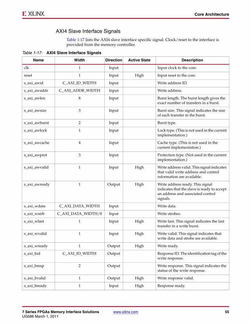
7 Series FPGAs Memory Interface Solutions www.xilinx.com 55UG586 March 1, 2011
Core Architecture
AXI4 Slave Interface Signals
Table 1-17 lists the AXI4 slave interface specific signal. Clock/reset to the interface is provided from the memory controller.
Table 1-17: AXI4 Slave Interface Signals
Name Width Direction Active State Description
clk 1 Input Input clock to the core.
reset 1 Input High Input reset to the core.
s_axi_awid C_AXI_ID_WIDTH Input Write address ID.
s_axi_awaddr C_AXI_ADDR_WIDTH Input Write address.
s_axi_awlen 8 Input Burst length. The burst length gives the exact number of transfers in a burst.
s_axi_awsize 3 Input Burst size. This signal indicates the size of each transfer in the burst.
s_axi_awburst 2 Input Burst type.
s_axi_awlock 1 Input Lock type. (This is not used in the current implementation.)
s_axi_awcache 4 Input Cache type. (This is not used in the current implementation.)
s_axi_awprot 3 Input Protection type. (Not used in the current implementation.)
s_axi_awvalid 1 Input High Write address valid. This signal indicates that valid write address and control information are available.
s_axi_awready 1 Output High Write address ready. This signal indicates that the slave is ready to accept an address and associated control signals.
s_axi_wdata C_AXI_DATA_WIDTH Input Write data.
s_axi_wstrb C_AXI_DATA_WIDTH/8 Input Write strobes.
s_axi_wlast 1 Input High Write last. This signal indicates the last transfer in a write burst.
s_axi_wvalid 1 Input High Write valid. This signal indicates that write data and strobe are available.
s_axi_wready 1 Output High Write ready.
s_axi_bid C_AXI_ID_WIDTH Output Response ID. The identification tag of the write response.
s_axi_bresp 2 Output Write response. This signal indicates the status of the write response.
s_axi_bvalid 1 Output High Write response valid.
s_axi_bready 1 Input High Response ready.
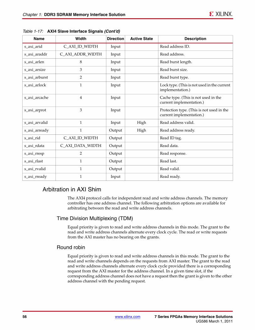
56 www.xilinx.com 7 Series FPGAs Memory Interface SolutionsUG586 March 1, 2011
Chapter 1: DDR3 SDRAM Memory Interface Solution
Arbitration in AXI ShimThe AXI4 protocol calls for independent read and write address channels. The memory controller has one address channel. The following arbitration options are available for arbitrating between the read and write address channels.
Time Division Multiplexing (TDM)
Equal priority is given to read and write address channels in this mode. The grant to the read and write address channels alternate every clock cycle. The read or write requests from the AXI master has no bearing on the grants.
Round robin
Equal priority is given to read and write address channels in this mode. The grant to the read and write channels depends on the requests from AXI master. The grant to the read and write address channels alternate every clock cycle provided there is a corresponding request from the AXI master for the address channel. In a given time slot, if the corresponding address channel does not have a request then the grant is given to the other address channel with the pending request.
s_axi_arid C_AXI_ID_WIDTH Input Read address ID.
s_axi_araddr C_AXI_ADDR_WIDTH Input Read address.
s_axi_arlen 8 Input Read burst length.
s_axi_arsize 3 Input Read burst size.
s_axi_arburst 2 Input Read burst type.
s_axi_arlock 1 Input Lock type. (This is not used in the current implementation.)
s_axi_arcache 4 Input Cache type. (This is not used in the current implementation.)
s_axi_arprot 3 Input Protection type. (This is not used in the current implementation.)
s_axi_arvalid 1 Input High Read address valid.
s_axi_arready 1 Output High Read address ready.
s_axi_rid C_AXI_ID_WIDTH Output Read ID tag.
s_axi_rdata C_AXI_DATA_WIDTH Output Read data.
s_axi_rresp 2 Output Read response.
s_axi_rlast 1 Output Read last.
s_axi_rvalid 1 Output Read valid.
s_axi_rready 1 Input Read ready.
Table 1-17: AXI4 Slave Interface Signals (Cont’d)
Name Width Direction Active State Description
7 Series FPGAs Memory Interface Solutions www.xilinx.com 57UG586 March 1, 2011
Core Architecture
Read priority
Read address channel is always given priority in this mode. The requests from the write address channel are processed when there are no pending requests from the read address channel.
Write priority
Write address channel is always given priority in this mode. The requests from the read address channel are processed when there are no pending requests from the read address channel.
User Interface BlockThe UI block presents the UI to a user design. It provides a simple alternative to the native interface. The UI block:
• Buffers read and write data
• Reorders read return data to match the request order
• Presents a flat address space and translates it to the addressing required by the SDRAM
Native InterfaceThe native interface connects to an FPGA user design to allow access to an external memory device.
Command Request Signals
The native interface provides a set of signals that request a read or write command from the memory controller to the memory device. These signals are summarized in Table 1-18.
Table 1-18: Native Interface Command Signals
Signal Direction Description
accept Output This output indicates that the memory interface accepts the request driven on the last cycle.
bank[2:0] Input This input selects the bank for the current request.
bank_mach_next[] Output This output is reserved and should be left unconnected.
cmd[2:0] Input This input selects the command for the current request.
col[COL_WIDTH – 1:0] Input This input selects the column address for the current request.
data_buf_addr[7:0] Input This input indicates the data buffer address where the memory controller:
• Locates data while processing write commands.
• Places data while processing read commands.
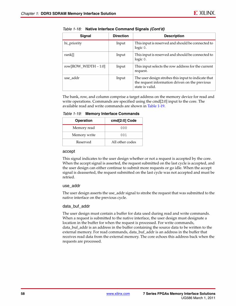
58 www.xilinx.com 7 Series FPGAs Memory Interface SolutionsUG586 March 1, 2011
Chapter 1: DDR3 SDRAM Memory Interface Solution
The bank, row, and column comprise a target address on the memory device for read and write operations. Commands are specified using the cmd[2:0] input to the core. The available read and write commands are shown in Table 1-19.
accept
This signal indicates to the user design whether or not a request is accepted by the core. When the accept signal is asserted, the request submitted on the last cycle is accepted, and the user design can either continue to submit more requests or go idle. When the accept signal is deasserted, the request submitted on the last cycle was not accepted and must be retried.
use_addr
The user design asserts the use_addr signal to strobe the request that was submitted to the native interface on the previous cycle.
data_buf_addr
The user design must contain a buffer for data used during read and write commands. When a request is submitted to the native interface, the user design must designate a location in the buffer for when the request is processed. For write commands, data_buf_addr is an address in the buffer containing the source data to be written to the external memory. For read commands, data_buf_addr is an address in the buffer that receives read data from the external memory. The core echoes this address back when the requests are processed.
hi_priority Input This input is reserved and should be connected to logic 0.
rank[] Input This input is reserved and should be connected to logic 0.
row[ROW_WIDTH – 1:0] Input This input selects the row address for the current request.
use_addr Input The user design strobes this input to indicate that the request information driven on the previous state is valid.
Table 1-19: Memory Interface Commands
Operation cmd[2:0] Code
Memory read 000
Memory write 001
Reserved All other codes
Table 1-18: Native Interface Command Signals (Cont’d)
Signal Direction Description
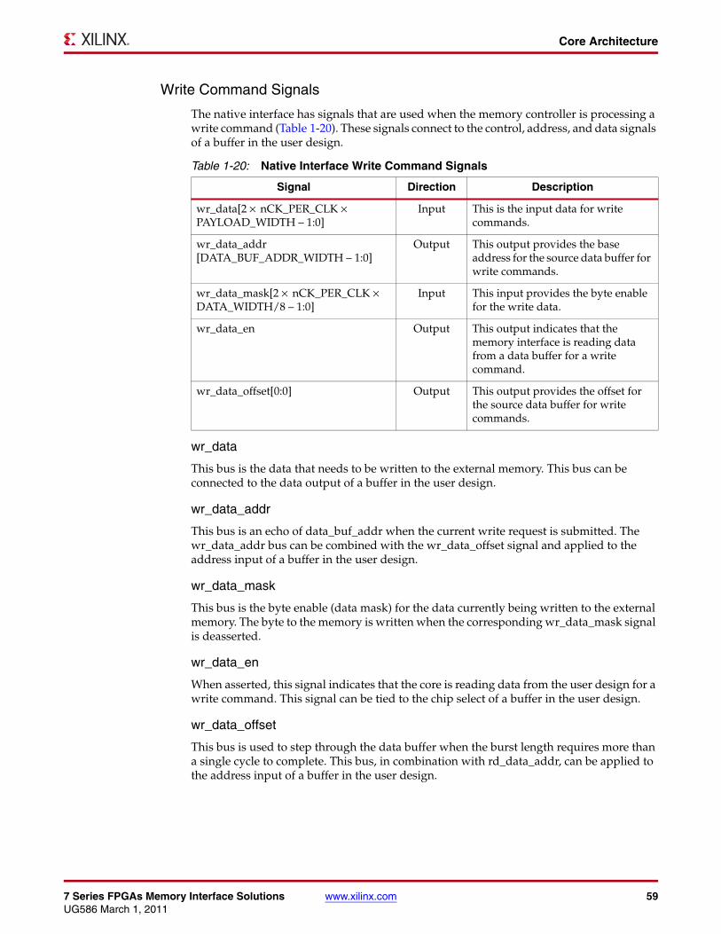
7 Series FPGAs Memory Interface Solutions www.xilinx.com 59UG586 March 1, 2011
Core Architecture
Write Command Signals
The native interface has signals that are used when the memory controller is processing a write command (Table 1-20). These signals connect to the control, address, and data signals of a buffer in the user design.
wr_data
This bus is the data that needs to be written to the external memory. This bus can be connected to the data output of a buffer in the user design.
wr_data_addr
This bus is an echo of data_buf_addr when the current write request is submitted. The wr_data_addr bus can be combined with the wr_data_offset signal and applied to the address input of a buffer in the user design.
wr_data_mask
This bus is the byte enable (data mask) for the data currently being written to the external memory. The byte to the memory is written when the corresponding wr_data_mask signal is deasserted.
wr_data_en
When asserted, this signal indicates that the core is reading data from the user design for a write command. This signal can be tied to the chip select of a buffer in the user design.
wr_data_offset
This bus is used to step through the data buffer when the burst length requires more than a single cycle to complete. This bus, in combination with rd_data_addr, can be applied to the address input of a buffer in the user design.
Table 1-20: Native Interface Write Command Signals
Signal Direction Description
wr_data[2 × nCK_PER_CLK × PAYLOAD_WIDTH – 1:0]
Input This is the input data for write commands.
wr_data_addr[DATA_BUF_ADDR_WIDTH – 1:0]
Output This output provides the base address for the source data buffer for write commands.
wr_data_mask[2 × nCK_PER_CLK × DATA_WIDTH/8 – 1:0]
Input This input provides the byte enable for the write data.
wr_data_en Output This output indicates that the memory interface is reading data from a data buffer for a write command.
wr_data_offset[0:0] Output This output provides the offset for the source data buffer for write commands.
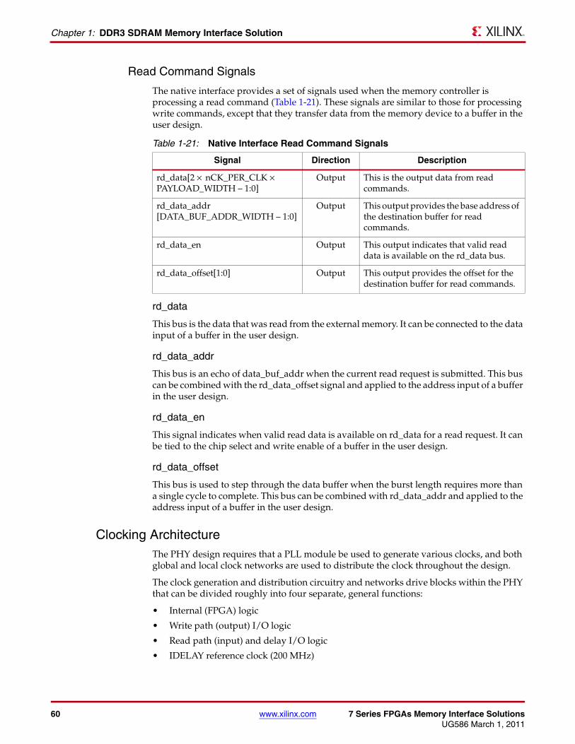
60 www.xilinx.com 7 Series FPGAs Memory Interface SolutionsUG586 March 1, 2011
Chapter 1: DDR3 SDRAM Memory Interface Solution
Read Command Signals
The native interface provides a set of signals used when the memory controller is processing a read command (Table 1-21). These signals are similar to those for processing write commands, except that they transfer data from the memory device to a buffer in the user design.
rd_data
This bus is the data that was read from the external memory. It can be connected to the data input of a buffer in the user design.
rd_data_addr
This bus is an echo of data_buf_addr when the current read request is submitted. This bus can be combined with the rd_data_offset signal and applied to the address input of a buffer in the user design.
rd_data_en
This signal indicates when valid read data is available on rd_data for a read request. It can be tied to the chip select and write enable of a buffer in the user design.
rd_data_offset
This bus is used to step through the data buffer when the burst length requires more than a single cycle to complete. This bus can be combined with rd_data_addr and applied to the address input of a buffer in the user design.
Clocking ArchitectureThe PHY design requires that a PLL module be used to generate various clocks, and both global and local clock networks are used to distribute the clock throughout the design.
The clock generation and distribution circuitry and networks drive blocks within the PHY that can be divided roughly into four separate, general functions:
• Internal (FPGA) logic
• Write path (output) I/O logic
• Read path (input) and delay I/O logic
• IDELAY reference clock (200 MHz)
Table 1-21: Native Interface Read Command Signals
Signal Direction Description
rd_data[2 × nCK_PER_CLK × PAYLOAD_WIDTH – 1:0]
Output This is the output data from read commands.
rd_data_addr[DATA_BUF_ADDR_WIDTH – 1:0]
Output This output provides the base address of the destination buffer for read commands.
rd_data_en Output This output indicates that valid read data is available on the rd_data bus.
rd_data_offset[1:0] Output This output provides the offset for the destination buffer for read commands.
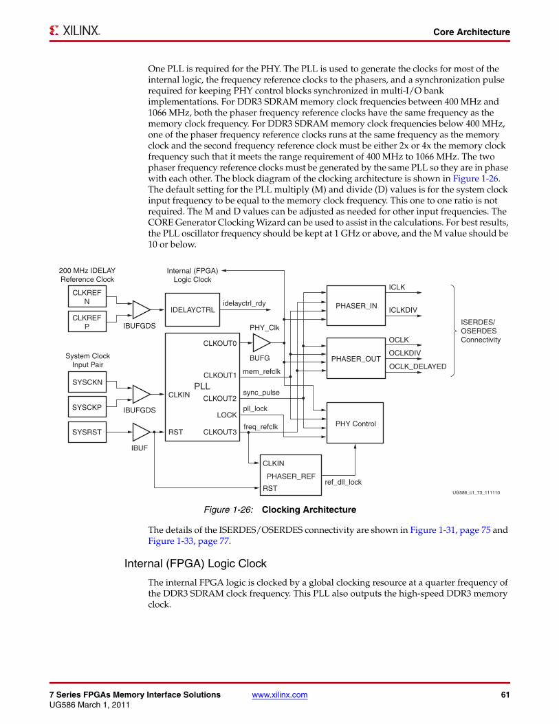
7 Series FPGAs Memory Interface Solutions www.xilinx.com 61UG586 March 1, 2011
Core Architecture
One PLL is required for the PHY. The PLL is used to generate the clocks for most of the internal logic, the frequency reference clocks to the phasers, and a synchronization pulse required for keeping PHY control blocks synchronized in multi-I/O bank implementations. For DDR3 SDRAM memory clock frequencies between 400 MHz and 1066 MHz, both the phaser frequency reference clocks have the same frequency as the memory clock frequency. For DDR3 SDRAM memory clock frequencies below 400 MHz, one of the phaser frequency reference clocks runs at the same frequency as the memory clock and the second frequency reference clock must be either 2x or 4x the memory clock frequency such that it meets the range requirement of 400 MHz to 1066 MHz. The two phaser frequency reference clocks must be generated by the same PLL so they are in phase with each other. The block diagram of the clocking architecture is shown in Figure 1-26. The default setting for the PLL multiply (M) and divide (D) values is for the system clock input frequency to be equal to the memory clock frequency. This one to one ratio is not required. The M and D values can be adjusted as needed for other input frequencies. The CORE Generator Clocking Wizard can be used to assist in the calculations. For best results, the PLL oscillator frequency should be kept at 1 GHz or above, and the M value should be 10 or below.
The details of the ISERDES/OSERDES connectivity are shown in Figure 1-31, page 75 and Figure 1-33, page 77.
Internal (FPGA) Logic Clock
The internal FPGA logic is clocked by a global clocking resource at a quarter frequency of the DDR3 SDRAM clock frequency. This PLL also outputs the high-speed DDR3 memory clock.
X-Ref Target - Figure 1-26
Figure 1-26: Clocking Architecture
200 MHz IDELAYReference Clock
Internal (FPGA)Logic Clock
idelayctrl_rdy
PHY_Clk
System ClockInput Pair
CLKREFN
PLLSYSCKN
IDELAYCTRL
SYSCKP
SYSRST
CLKREFP
CLKIN
CLKIN
ref_dll_lockRST
CLKOUT0
CLKOUT1
CLKOUT2
CLKOUT3
LOCK
RSTfreq_refclk
pll_lock
sync_pulse
mem_refclk
BUFG
IBUFGDS
IBUFGDS
IBUF
PHASER_REF
PHASER_IN
PHASER_OUT
PHY Control
ISERDES/OSERDES Connectivity
ICLK
OCLK
OCLK_DELAYED
OCLKDIV
ICLKDIV
UG586_c1_73_111110
62 www.xilinx.com 7 Series FPGAs Memory Interface SolutionsUG586 March 1, 2011
Chapter 1: DDR3 SDRAM Memory Interface Solution
Write Path (Output) I/O Logic Clock
The output path comprising both data and controls is clocked by PHASER_OUT. The PHASER_OUT provides synchronized clocks for each byte group to the OUT_FIFOs and to the OSERDES/ODDR. The PHASER_OUT generates a byte clock (OCLK), a divided byte clock (OCLKDIV), and a delayed byte clock (OCLK_DELAYED) for its associated byte group. These clocks are generated directly from the Frequency Reference clock and are in phase with each other. The byte clock is the same frequency as the Frequency Reference clock and the divided byte clock is half the frequency of the Frequency Reference clock. OCLK_DELAYED is used to clock the DQS ODDR to achieve the required 90-degree phase offset between the write DQS and its associated DQ bits. The PHASER_OUT also drives the signalling required to generate DQS during writes, the DQS and DQ 3-state associated with the data byte group, and the Read Enable for the OUT_FIFO of the byte group. The clocking details of the address/control and the write paths using PHASER_OUT are shown in Figure 1-31 and Figure 1-33.
Read Path (Input) I/O Logic Clock
The input read datapath is clocked by the PHASER_IN block. The PHASER_IN block provides synchronized clocks for each byte group to the IN_FIFOs and to the IDDR/ISERDES. The PHASER_IN block receives the DQS signal for the associated byte group and generates two delayed clocks for DDR3 SDRAM data captures: read byte clock (ICLK) and read divided byte clock (ICLKDIV). ICLK is the delayed version of the frequency reference clock that is phase-aligned with its associated DQS. ICLKDIV is used to capture data into the first rank of flip-flops in the ISERDES. ICLKDIV is aligned to ICLK and is the parallel transfer clock for the last rank of flip-flops in the ISERDES. ICLKDIV is also used as the write clock for the IN_FIFO associated with the byte group. The PHASER_IN block also drives the write enable (WrEnable) for the IN_FIFO of the byte group. The clocking details of the read path using PHASER_IN is shown in Figure 1-33.
IDELAY Reference Clock
A 200 MHz IDELAY clock must be supplied to the IDELAYCTRL module. The IDELAYCTRL module continuously calibrates the IDELAY elements in the I/O region to account for varying environmental conditions. The IP core assumes an external clock signal is driving the IDELAYCTRL module. If a PLL clock drives the IDELAYCTRL input clock, the PLL lock signal needs to be incorporated in the rst_tmp_idelay signal inside the IODELAY_CTRL.v/vhd module. This ensures that the clock is stable before being used.
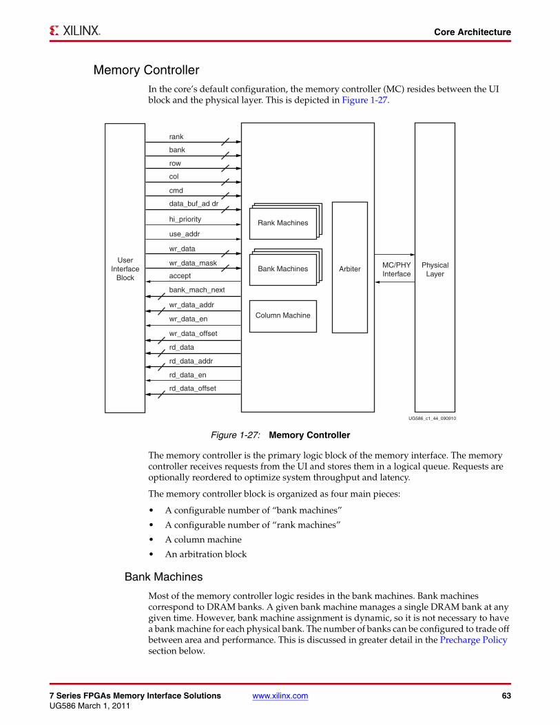
7 Series FPGAs Memory Interface Solutions www.xilinx.com 63UG586 March 1, 2011
Core Architecture
Memory ControllerIn the core’s default configuration, the memory controller (MC) resides between the UI block and the physical layer. This is depicted in Figure 1-27.
The memory controller is the primary logic block of the memory interface. The memory controller receives requests from the UI and stores them in a logical queue. Requests are optionally reordered to optimize system throughput and latency.
The memory controller block is organized as four main pieces:
• A configurable number of “bank machines”
• A configurable number of “rank machines”
• A column machine
• An arbitration block
Bank Machines
Most of the memory controller logic resides in the bank machines. Bank machines correspond to DRAM banks. A given bank machine manages a single DRAM bank at any given time. However, bank machine assignment is dynamic, so it is not necessary to have a bank machine for each physical bank. The number of banks can be configured to trade off between area and performance. This is discussed in greater detail in the Precharge Policy section below.
X-Ref Target - Figure 1-27
Figure 1-27: Memory Controller
rank
bank
row
col
cmd
data_buf_ad dr
hi_priority
use_addr
wr_data
wr_data_mask
accept
bank_mach_next
wr_data_addr
wr_data_en
wr_data_offset
rd_data
rd_data_addr
rd_data_en
rd_data_offset
Rank Machines
Bank Machines Arbiter MC/PHYInterface
PhysicalLayer
UserInterface
Block
Column Machine
UG586_c1_44_090910
64 www.xilinx.com 7 Series FPGAs Memory Interface SolutionsUG586 March 1, 2011
Chapter 1: DDR3 SDRAM Memory Interface Solution
The duration of a bank machine's assignment to a particular DRAM bank is coupled to user requests rather than the state of the target DRAM bank. When a request is accepted, it is assigned to a bank machine. When a request is complete, the bank machine is released and is made available for assignment to another request. Bank machines issue all the commands necessary to complete the request.
On behalf of the current request, a bank machine must generate row commands and column commands to complete the request. Row and column commands are independent but must adhere to DRAM timing requirements.
The following simplified example illustrates this concept. Consider the case when the memory controller and DRAM are idle when a single request arrives. The bank machine at the head of the pool:
1. Accepts the user request
2. Activates the target row
3. Issues the column (read or write) command
4. Precharges the target row
5. Returns to the idle pool of bank machines
Similar functionality applies when multiple requests arrive targeting different rows or banks.
Now consider the case when a request arrives targeting an open DRAM bank, managed by an already active bank machine. The already active bank machine recognizes that the new request targets the same DRAM bank and skips the precharge step (step 4). The bank machine at the head of the idle pool accepts the new user request and skips the activate step (step 2).
Finally, when a request arrives in between both a previous and subsequent request all to the same target DRAM bank, the controller skips both the activate (step 2) and precharge (step 4) operations.
A bank machine precharges a DRAM bank as soon as possible unless another pending request targets the same bank. This is discussed in greater detail in the Precharge Policy section.
Column commands can be reordered for the purpose of optimizing memory interface throughput. The ordering algorithm nominally ensures data coherence. The reordering feature is explained in greater detail in the Reordering section.
Rank Machines
The rank machines correspond to DRAM ranks. Rank machines monitor the activity of the bank machines and track rank or device-specific timing parameters. For example, a rank machine monitors the number of activate commands sent to a rank within a time window. After the allowed number of activates have been sent, the rank machine generates an inhibit signal that prevents the bank machines from sending any further activates to the rank until the time window has shifted enough to allow more activates. Rank machines are statically assigned to a physical DRAM rank.
Column Machine
The single column machine generates the timing information necessary to manage the DQ data bus. Although there can be multiple DRAM ranks, because there is a single DQ bus, all the columns in all DRAM ranks are managed as a single unit. The column machine
7 Series FPGAs Memory Interface Solutions www.xilinx.com 65UG586 March 1, 2011
Core Architecture
monitors commands issued by the bank machines and generates inhibit signals back to the bank machines so that the DQ bus is utilized in an orderly manner.
Arbitration Block
The arbitration block receives requests to send commands to the DRAM array from the bank machines. Row commands and column commands are arbitrated independently. For each command opportunity, the arbiter block selects a row and a column command to forward to the physical layer. The arbitration block implements a round-robin protocol to ensure forward progress.
Reordering
DRAM accesses are broken into two quasi-independent parts, row commands and column commands. Each request occupies a logical queue entry, and each queue entry has an associated bank machine. These bank machines track the state of the DRAM rank or bank it is currently bound to, if any.
If necessary, the bank machine attempts to activate the proper rank, bank, or row on behalf of the current request. In the process of doing so, the bank machine looks at the current state of the DRAM to decide if various timing parameters are met. Eventually, all timing parameters are met and the bank machine arbitrates to send the activate. The arbitration is done in a simple round-robin manner. Arbitration is necessary because several bank machines might request to send row commands (activate and precharge) at the same time.
Not all requests require an activate. If a preceding request has activated the same rank, bank, or row, a subsequent request might inherit the bank machine state and avoid the precharge/activate penalties.
After the necessary rank, bank, or row is activated and the RAS to CAS delay timing is met, the bank machine tries to issue the CAS-READ or CAS-WRITE command. Unlike the row command, all requests issue a CAS command. Before arbitrating to send a CAS command, the bank machine must look at the state of the DRAM, the state of the DQ bus, priority, and ordering. Eventually, all these factors assume their favorable states and the bank machine arbitrates to send a CAS command. In a manner similar to row commands, a round-robin arbiter uses a priority scheme and selects the next column command.
The round-robin arbiter itself is a source of reordering. Assume for example that an otherwise idle memory controller receives a burst of new requests while processing a refresh. These requests queue up and wait for the refresh to complete. After the DRAM is ready to receive a new activate, all waiting requests assert their arbitration requests simultaneously. The arbiter selects the next activate to send based solely on its round-robin algorithm, independent of request order. Similar behavior can be observed for column commands.
Precharge Policy
The controller implements an aggressive precharge policy. The controller examines the input queue of requests as each transaction completes. If no requests are in the queue for a currently open bank/row, the controller closes it to minimize latency for requests to other rows in the bank. Because the queue depth is equal to the number of bank machines, greater efficiency can be obtained by increasing the number of bank machines (nBANK_MACHS). As this number is increased, fabric timing becomes more challenging. In some situations, the overall system efficiency can be greater with an increased number of bank machines and a lower memory clock frequency. Simulations should be performed with the target design's command behavior to determine the optimum setting.
66 www.xilinx.com 7 Series FPGAs Memory Interface SolutionsUG586 March 1, 2011
Chapter 1: DDR3 SDRAM Memory Interface Solution
PHYThe PHY provides a physical interface to an external DDR3 SDRAM. The PHY generates the signal timing and sequencing required to interface to the memory device. It contains the clock-, address-, and control-generation logic, write and read datapaths, and state logic for initializing the SDRAM after power-up. In addition, the PHY contains calibration logic to perform timing training of the read and write datapaths to account for system static and dynamic delays.
The PHY is provided as a single HDL codebase for DDR3 SDRAMs. The MIG tool customizes the SDRAM type and numerous other design-specific parameters through top-level HDL parameters and constraints contained in a user constraints file (UCF).
Overall PHY Architecture
The 7 series FPGA PHY is composed of dedicated blocks and soft calibration logic. The dedicated blocks are structured adjacent to one another with back-to-back interconnects to minimize the clock and datapath routing necessary to build high-performance physical layers. Dedicated clock structures within an I/O bank referred to as byte group clocks help minimize the number of loads driven by the byte group clock drivers. Byte group clocks are driven by phaser blocks. The phaser blocks (PHASER_IN and PHASER_OUT) are multi-stage programmable delay line loops that can dynamically track DQS signal variation and provide precision phase adjustment.
Each 7 series FPGA I/O bank has dedicated blocks comprising a PHY control block, four PHASER_IN and PHASER_OUT blocks, four IN/OUT_FIFOs, IOLOGIC (ISERDES, OSERDES, ODDR, IDELAY), and IOBs. Four byte groups exist in an I/O bank, and each byte group contains the PHASER_IN and PHASER_OUT, IN_FIFO and OUT_FIFO, and twelve IOLOGIC and IOB blocks. Ten of the twelve IOIs in a byte group are used for DQ and DM bits, and the other two IOIs are used to implement differential DQS signals. Figure 1-28 shows the dedicated blocks available in a single I/O bank. A single PHY control block communicates with all four PHASER_IN and PHASER_OUT blocks within the I/O bank.
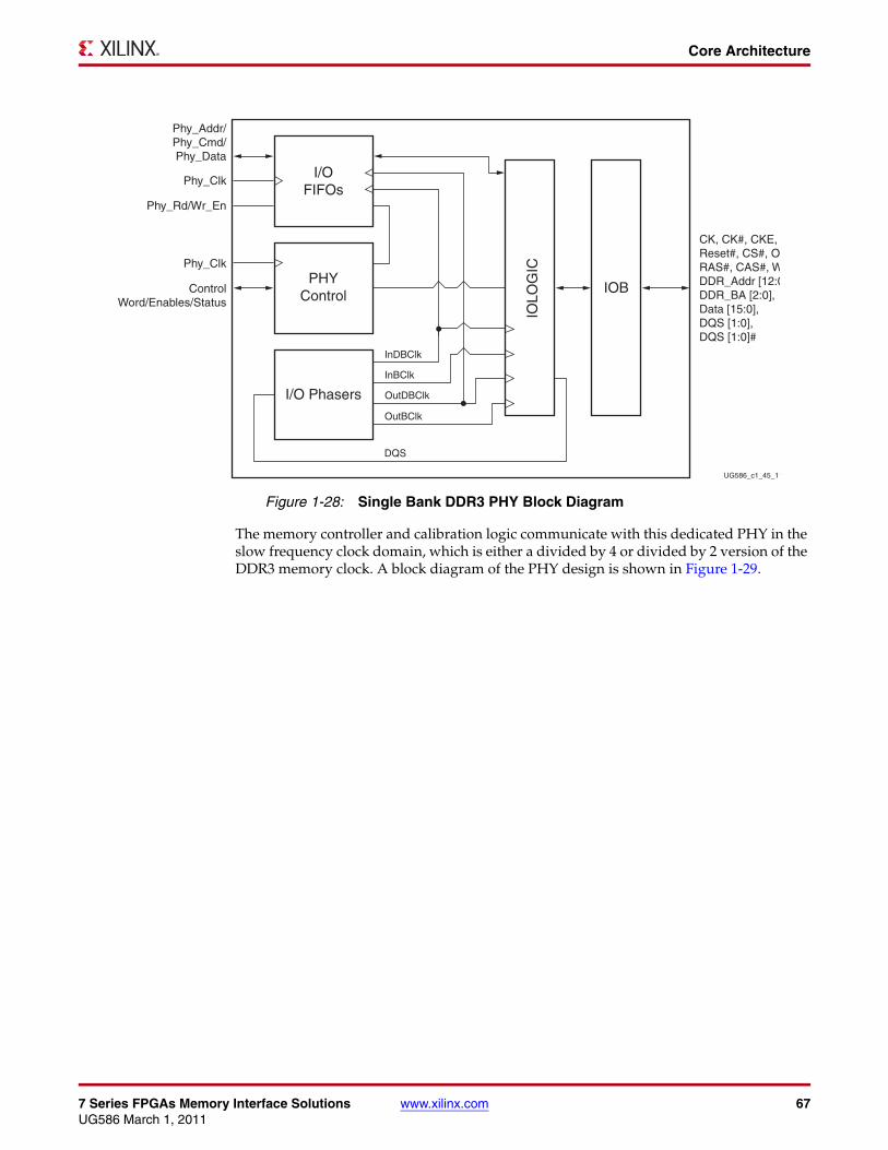
7 Series FPGAs Memory Interface Solutions www.xilinx.com 67UG586 March 1, 2011
Core Architecture
The memory controller and calibration logic communicate with this dedicated PHY in the slow frequency clock domain, which is either a divided by 4 or divided by 2 version of the DDR3 memory clock. A block diagram of the PHY design is shown in Figure 1-29.
X-Ref Target - Figure 1-28
Figure 1-28: Single Bank DDR3 PHY Block Diagram
I/OFIFOs
PHYControl
IOLO
GIC
IOB
CK, CK#, CKE,Reset#, CS#, ORAS#, CAS#, WDDR_Addr [12:0DDR_BA [2:0],Data [15:0],DQS [1:0],DQS [1:0]#
I/O Phasers
DQS
OutBClk
OutDBClk
InBClk
InDBClk
Phy_Addr/ Phy_Cmd/ Phy_Data
Phy_Rd/Wr_En
Phy_Clk
UG586_c1_45_11
ControlWord/Enables/Status
Phy_Clk
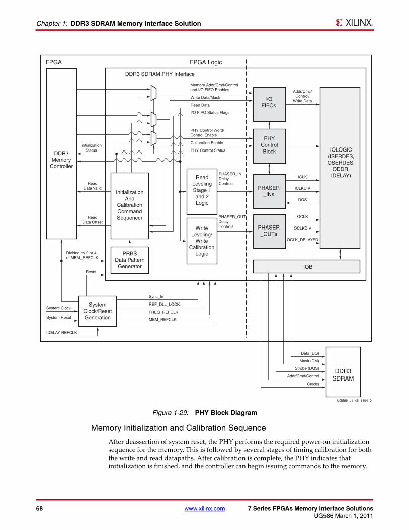
68 www.xilinx.com 7 Series FPGAs Memory Interface SolutionsUG586 March 1, 2011
Chapter 1: DDR3 SDRAM Memory Interface Solution
Memory Initialization and Calibration Sequence
After deassertion of system reset, the PHY performs the required power-on initialization sequence for the memory. This is followed by several stages of timing calibration for both the write and read datapaths. After calibration is complete, the PHY indicates that initialization is finished, and the controller can begin issuing commands to the memory.
X-Ref Target - Figure 1-29
Figure 1-29: PHY Block Diagram
IOLOGIC(ISERDES,OSERDES,
ODDR,IDELAY)
DDR2/DDR3
SDRAM
I/OFIFOs
FPGA
DDR2/DDR3 SDRAM PHY Interface
FPGA Logic
PHYControlBlock
PHASER_INs
PHASER_OUTs
UG586_c1_46_110410
Memory Addr/Cmd/Controland I/O FIFO Enables
Write Data/Mask
Read Data
I/O FIFO Status Flags
PHY Control Word/Control Enable
Calibration EnableInitialization
Status
ReadData Valid
PHASER_INDelayControls
PHASER_OUTDelayControls
PHY Control Status
ICLK
Addr/Cmc/Control/
Write Data
ICLKDIV
DQS
OCLK
OCLKDIV
OCLK_DELAYED
Clocks
Addr/Cmd/Control
Strobe (DQS)
Mask (DM)
Data (DQ)
System Clock
Reset
Divided by 2 or 4of MEM_REFCLK
System Reset
IDELAY REFCLK
ReadData Offset
IOB
WriteLeveling/
WriteCalibration
Logic
ReadLevelingStage 1and 2Logic
InitializationAnd
CalibrationCommandSequencer
DDR2/DDR3
MemoryController
PRBSData PatternGenerator
SystemClock/ResetGeneration
REF_DLL_LOCK
Sync_In
FREQ_REFCLK
MEM_REFCLK
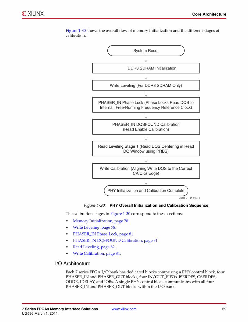
7 Series FPGAs Memory Interface Solutions www.xilinx.com 69UG586 March 1, 2011
Core Architecture
Figure 1-30 shows the overall flow of memory initialization and the different stages of calibration.
The calibration stages in Figure 1-30 correspond to these sections:
• Memory Initialization, page 78.
• Write Leveling, page 78.
• PHASER_IN Phase Lock, page 81.
• PHASER_IN DQSFOUND Calibration, page 81.
• Read Leveling, page 82.
• Write Calibration, page 84.
I/O Architecture
Each 7 series FPGA I/O bank has dedicated blocks comprising a PHY control block, four PHASER_IN and PHASER_OUT blocks, four IN/OUT_FIFOs, ISERDES, OSERDES, ODDR, IDELAY, and IOBs. A single PHY control block communicates with all four PHASER_IN and PHASER_OUT blocks within the I/O bank.
X-Ref Target - Figure 1-30
Figure 1-30: PHY Overall Initialization and Calibration Sequence
UG586_c1_47_110410
DDR2/DDR3 SDRAM Initialization
Write Leveling (For DDR3 SDRAM Only)
PHASER_IN DQSFOUND Calibration(Read Enable Calibration)
PHASER_IN Phase Lock (Phase Locks Read DQS toInternal, Free-Running Frequency Reference Clock)
Read Leveling Stage 1 (Read DQS Centering in ReadDQ Window using PRBS)
Write Calibration (Aligning Write DQS to the CorrectCK/CK# Edge)
System Reset
PHY Initialization and Calibration Complete
70 www.xilinx.com 7 Series FPGAs Memory Interface SolutionsUG586 March 1, 2011
Chapter 1: DDR3 SDRAM Memory Interface Solution
PHY Control Block
The PHY control block is the central control block that manages the flow of data and control information between the FPGA logic and the dedicated PHY. This includes control over the flow of address, command, and data between the IN/OUT_FIFOs and ISERDES/OSERDES, and control of the PHASER_IN and PHASER_OUT blocks. The PHY control block receives control words from the calibration logic or the memory controller at the slow frequency (1/4 the frequency of the DDR3 SDRAM clock) PHY_Clk rate and processes the control words at the DDR3 SDRAM clock rate (CK frequency).
The calibration logic or the memory controller initiates a DDR3 SDRAM command sequence by writing address, command, and data (for write commands) into the IN/OUT_FIFOs and simultaneously or subsequently writes the PHY control word to the PHY control block. The PHY control word defines a set of actions that the PHY control block does to initiate the execution of a DDR3 SDRAM command.
The PHY control block provides the control interfaces to the byte group blocks within its I/O bank. When multi-I/O bank implementations are required, each PHY control block within a given I/O bank controls the byte group elements in that bank. This requires that the PHY control blocks stay in phase with their adjacent PHY control blocks. The center PHY control block is configured to be the master controller for a three I/O bank implementation. For two bank implementations, either PHY control block can be designated the master.
The PHY control interface is used by the calibration logic or the memory controller to write PHY control words to the PHY. The signals in this interface are synchronous to the PHY_Clk and are listed in Table 1-22. This is a basic FIFO style interface. Control words are written into the control word FIFO on the rising edge of PHY_Clk when PHY_Ctl_WrEn is high and PHY_Ctl_Full is Low. For multi-I/O bank PHYs, the same control word must be written into each PHY control block for proper operation.
The PHY control word is broken down into several fields, as shown in Table 1-23.
Table 1-22: PHY Control Interface
Signal Direction Signal Description
PHY_Clk Input This is the PHY interface clock for the control word FIFO. PHY control word signals are captured on the rising edge of this clock.
PHY_Ctl_Wr_N Input This active-Low signal is the write enable signal for the control word FIFO. A control word is written into the control word FIFO on the rising edge of PHY_Clk, when this signal is active.
PHY_Ctl_Wd[31:0] Input This is the PHY control word described in Table 1-23.
PHY_Ctl_Full Output This active high output is the full flag for the control word FIFO. It indicates that the FIFO cannot accept any more control words and blocks writes to the control word FIFO.
PHY_Ctl_AlmostFull Output This active high output is the almost full flag for the control word FIFO. It indicates that the FIFO can accept no more than one additional control word as long as the PHY_Ctl_Full signal is inactive.
PHY_Ctl_Ready Output This active high output becomes set when the PHY control block is ready to start receiving commands.
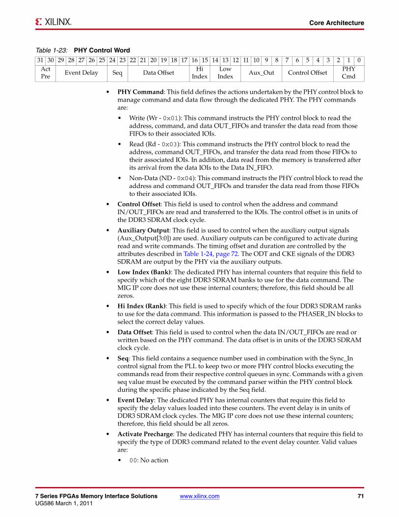
7 Series FPGAs Memory Interface Solutions www.xilinx.com 71UG586 March 1, 2011
Core Architecture
• PHY Command: This field defines the actions undertaken by the PHY control block to manage command and data flow through the dedicated PHY. The PHY commands are:
• Write (Wr - 0x01): This command instructs the PHY control block to read the address, command, and data OUT_FIFOs and transfer the data read from those FIFOs to their associated IOIs.
• Read (Rd - 0x03): This command instructs the PHY control block to read the address, command OUT_FIFOs, and transfer the data read from those FIFOs to their associated IOIs. In addition, data read from the memory is transferred after its arrival from the data IOIs to the Data IN_FIFO.
• Non-Data (ND - 0x04): This command instructs the PHY control block to read the address and command OUT_FIFOs and transfer the data read from those FIFOs to their associated IOIs.
• Control Offset: This field is used to control when the address and command IN/OUT_FIFOs are read and transferred to the IOIs. The control offset is in units of the DDR3 SDRAM clock cycle.
• Auxiliary Output: This field is used to control when the auxiliary output signals (Aux_Output[3:0]) are used. Auxiliary outputs can be configured to activate during read and write commands. The timing offset and duration are controlled by the attributes described in Table 1-24, page 72. The ODT and CKE signals of the DDR3 SDRAM are output by the PHY via the auxiliary outputs.
• Low Index (Bank): The dedicated PHY has internal counters that require this field to specify which of the eight DDR3 SDRAM banks to use for the data command. The MIG IP core does not use these internal counters; therefore, this field should be all zeros.
• Hi Index (Rank): This field is used to specify which of the four DDR3 SDRAM ranks to use for the data command. This information is passed to the PHASER_IN blocks to select the correct delay values.
• Data Offset: This field is used to control when the data IN/OUT_FIFOs are read or written based on the PHY command. The data offset is in units of the DDR3 SDRAM clock cycle.
• Seq: This field contains a sequence number used in combination with the Sync_In control signal from the PLL to keep two or more PHY control blocks executing the commands read from their respective control queues in sync. Commands with a given seq value must be executed by the command parser within the PHY control block during the specific phase indicated by the Seq field.
• Event Delay: The dedicated PHY has internal counters that require this field to specify the delay values loaded into these counters. The event delay is in units of DDR3 SDRAM clock cycles. The MIG IP core does not use these internal counters; therefore, this field should be all zeros.
• Activate Precharge: The dedicated PHY has internal counters that require this field to specify the type of DDR3 command related to the event delay counter. Valid values are:
• 00: No action
Table 1-23: PHY Control Word31 30 29 28 27 26 25 24 23 22 21 20 19 18 17 16 15 14 13 12 11 10 9 8 7 6 5 4 3 2 1 0
Act Pre Event Delay Seq Data Offset
Hi Index
Low Index Aux_Out Control Offset
PHY Cmd
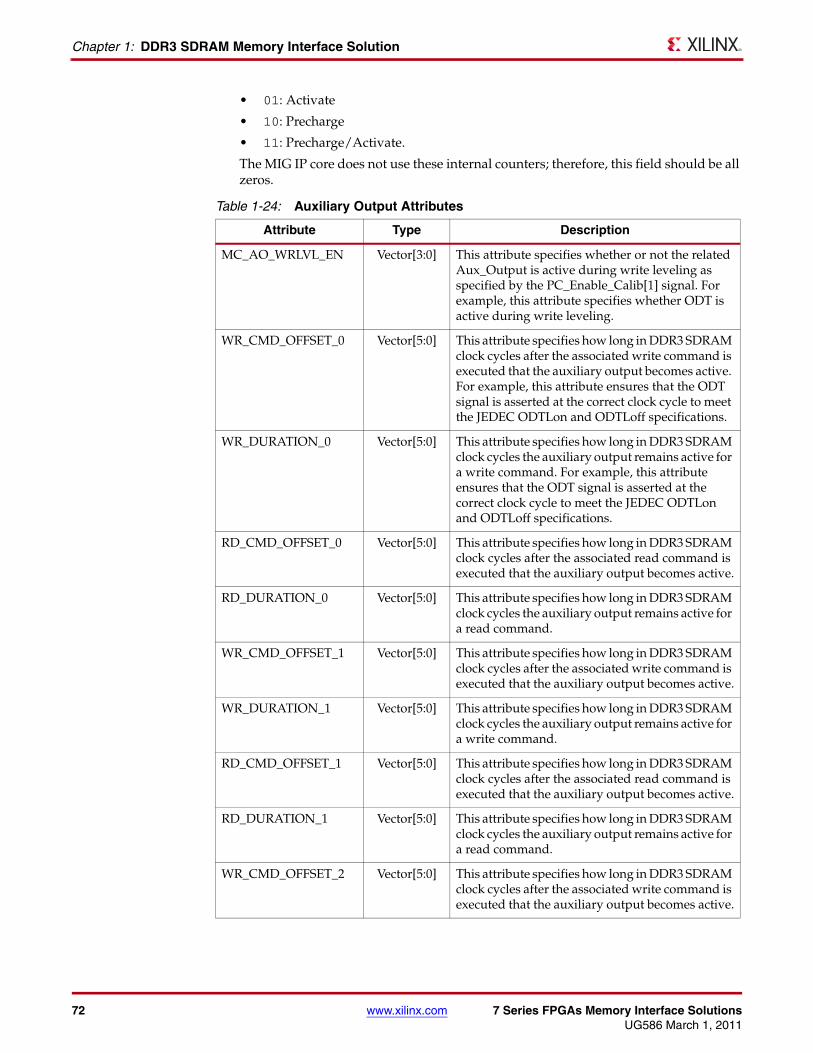
72 www.xilinx.com 7 Series FPGAs Memory Interface SolutionsUG586 March 1, 2011
Chapter 1: DDR3 SDRAM Memory Interface Solution
• 01: Activate
• 10: Precharge
• 11: Precharge/Activate.
The MIG IP core does not use these internal counters; therefore, this field should be all zeros.
Table 1-24: Auxiliary Output Attributes
Attribute Type Description
MC_AO_WRLVL_EN Vector[3:0] This attribute specifies whether or not the related Aux_Output is active during write leveling as specified by the PC_Enable_Calib[1] signal. For example, this attribute specifies whether ODT is active during write leveling.
WR_CMD_OFFSET_0 Vector[5:0] This attribute specifies how long in DDR3 SDRAM clock cycles after the associated write command is executed that the auxiliary output becomes active. For example, this attribute ensures that the ODT signal is asserted at the correct clock cycle to meet the JEDEC ODTLon and ODTLoff specifications.
WR_DURATION_0 Vector[5:0] This attribute specifies how long in DDR3 SDRAM clock cycles the auxiliary output remains active for a write command. For example, this attribute ensures that the ODT signal is asserted at the correct clock cycle to meet the JEDEC ODTLon and ODTLoff specifications.
RD_CMD_OFFSET_0 Vector[5:0] This attribute specifies how long in DDR3 SDRAM clock cycles after the associated read command is executed that the auxiliary output becomes active.
RD_DURATION_0 Vector[5:0] This attribute specifies how long in DDR3 SDRAM clock cycles the auxiliary output remains active for a read command.
WR_CMD_OFFSET_1 Vector[5:0] This attribute specifies how long in DDR3 SDRAM clock cycles after the associated write command is executed that the auxiliary output becomes active.
WR_DURATION_1 Vector[5:0] This attribute specifies how long in DDR3 SDRAM clock cycles the auxiliary output remains active for a write command.
RD_CMD_OFFSET_1 Vector[5:0] This attribute specifies how long in DDR3 SDRAM clock cycles after the associated read command is executed that the auxiliary output becomes active.
RD_DURATION_1 Vector[5:0] This attribute specifies how long in DDR3 SDRAM clock cycles the auxiliary output remains active for a read command.
WR_CMD_OFFSET_2 Vector[5:0] This attribute specifies how long in DDR3 SDRAM clock cycles after the associated write command is executed that the auxiliary output becomes active.
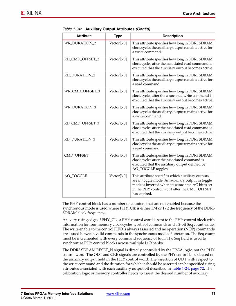
7 Series FPGAs Memory Interface Solutions www.xilinx.com 73UG586 March 1, 2011
Core Architecture
The PHY control block has a number of counters that are not enabled because the synchronous mode is used where PHY_Clk is either 1/4 or 1/2 the frequency of the DDR3 SDRAM clock frequency.
At every rising edge of PHY_Clk, a PHY control word is sent to the PHY control block with information for four memory clock cycles worth of commands and a 2-bit Seq count value. The write enable to the control FIFO is always asserted and no operation (NOP) commands are issued between valid commands in the synchronous mode of operation. The Seq count must be incremented with every command sequence of four. The Seq field is used to synchronize PHY control blocks across multiple I/O banks.
The DDR3 SDRAM RESET_N signal is directly controlled by the FPGA logic, not the PHY control word. The ODT and CKE signals are controlled by the PHY control block based on the auxiliary output field in the PHY control word. The assertion of ODT with respect to the write command and the duration for which it should be asserted can be specified using attributes associated with each auxiliary output bit described in Table 1-24, page 72. The calibration logic or memory controller needs to assert the desired number of auxiliary
WR_DURATION_2 Vector[5:0] This attribute specifies how long in DDR3 SDRAM clock cycles the auxiliary output remains active for a write command.
RD_CMD_OFFSET_2 Vector[5:0] This attribute specifies how long in DDR3 SDRAM clock cycles after the associated read command is executed that the auxiliary output becomes active.
RD_DURATION_2 Vector[5:0] This attribute specifies how long in DDR3 SDRAM clock cycles the auxiliary output remains active for a read command.
WR_CMD_OFFSET_3 Vector[5:0] This attribute specifies how long in DDR3 SDRAM clock cycles after the associated write command is executed that the auxiliary output becomes active.
WR_DURATION_3 Vector[5:0] This attribute specifies how long in DDR3 SDRAM clock cycles the auxiliary output remains active for a write command.
RD_CMD_OFFSET_3 Vector[5:0] This attribute specifies how long in DDR3 SDRAM clock cycles after the associated read command is executed that the auxiliary output becomes active.
RD_DURATION_3 Vector[5:0] This attribute specifies how long in DDR3 SDRAM clock cycles the auxiliary output remains active for a read command.
CMD_OFFSET Vector[5:0] This attribute specifies how long in DDR3 SDRAM clock cycles after the associated command is executed that the auxiliary output defined by AO_TOGGLE toggles.
AO_TOGGLE Vector[3:0] This attribute specifies which auxiliary outputs are in toggle mode. An auxiliary output in toggle mode is inverted when its associated AO bit is set in the PHY control word after the CMD_OFFSET has expired.
Table 1-24: Auxiliary Output Attributes (Cont’d)
Attribute Type Description

74 www.xilinx.com 7 Series FPGAs Memory Interface SolutionsUG586 March 1, 2011
Chapter 1: DDR3 SDRAM Memory Interface Solution
output bits and set the associated attributes with every write and read command request. The PHY control block, in conjunction with the PHASER_OUT, generates the write DQS and the DQ/DQS 3-state control signals during read and write commands.
The PHY cmd field is set based on whether the sequence of four commands has either a write, a read, or neither. The PHY cmd field is set to write if there is a write request in the command sequence. It is set to read if there is a read request in the command sequence, and it is set to non-data if there is neither a write nor a read request in the command sequence. A write and a read request cannot be issued within a sequence of four commands. The control offset field in the PHY control word defines when the command OUT_FIFOs is read out and transferred to the IOLOGIC. The data offset defines when the data OUT_FIFOs are read out with respect to the command OUT_FIFOs being read. For read commands, the data offset is determined during calibration. The PHY control block assumes that valid data associated with a write command is already available in the DQ OUT_FIFO when it is required to be read out.
Command Path
A command requested by the calibration logic or memory controller is sent out as a PHY control word to the PHY control block and a simultaneous input to the address/control/command OUT_FIFOs. Each of the address/control/command signals must have values for four memory clock cycles because each PHY_Clk cycle entails four memory clock cycles. Figure 1-31 shows the block diagram of the address/control/command path. The OSERDES is used in single data rate (SDR) mode because address/control/commands are SDR signals. A PHY control word is qualified with the Phy_Ctl_Wr_N signal and an entry to the OUT_FIFOs is qualified with the PHY_Cmd_WrEn signal. The FPGA logic need not issue NOP commands during long wait times between valid commands to the PHY control block because the default in the dedicated PHY for address/commands can be set to 0 or 1 as needed.
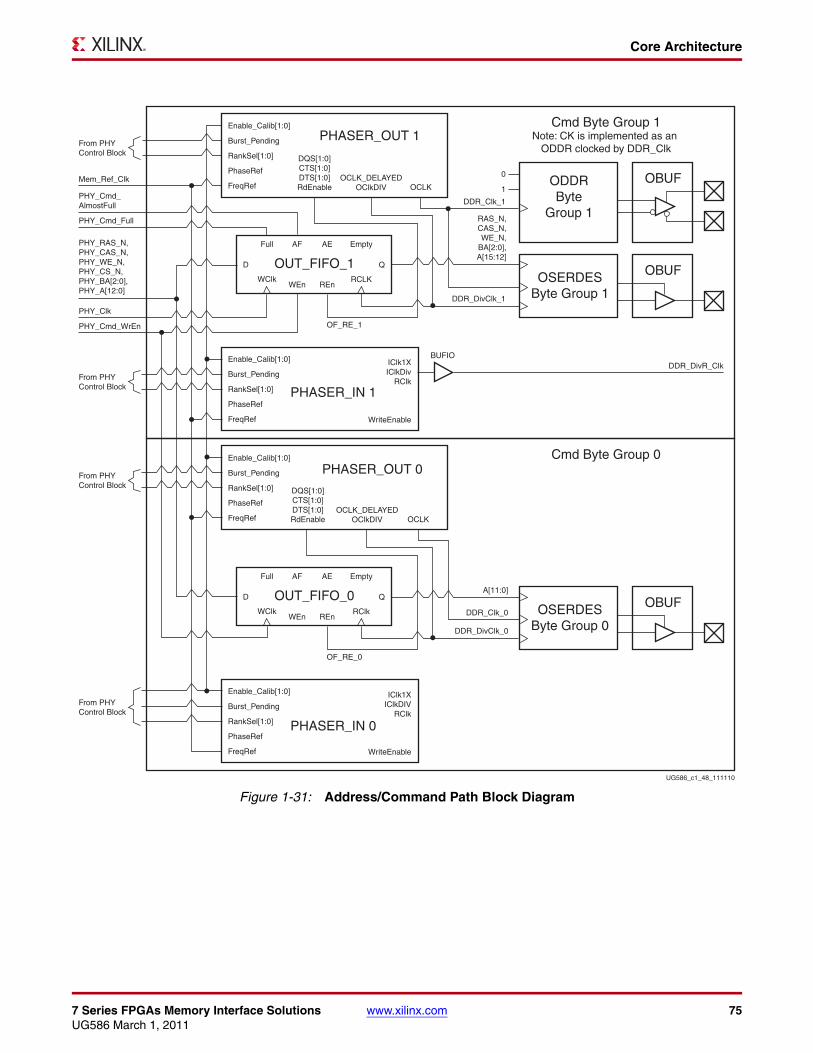
7 Series FPGAs Memory Interface Solutions www.xilinx.com 75UG586 March 1, 2011
Core Architecture
X-Ref Target - Figure 1-31
Figure 1-31: Address/Command Path Block Diagram
UG586_c1_48_111110
From PHYControl Block
Mem_Ref_Clk
PHY_Cmd_AlmostFull
PHY_Cmd_Full
PHY_Clk
DDR_DivClk_1
DDR_DivR_ClkBUFIO
DDR_Clk_1
RAS_N,CAS_N,WE_N,
BA[2:0],A[15:12]
OF_RE_1PHY_Cmd_WrEn
PHY_RAS_N,PHY_CAS_N,PHY_WE_N,PHY_CS_N,PHY_BA[2:0],PHY_A[12:0]
Enable_Calib[1:0]
Burst_Pending
RankSel[1:0]
OCLKOCLK_DELAYED
OClkDIV 1
0
DQS[1:0]CTS[1:0]DTS[1:0]RdEnable
PhaseRef
FreqRef
PHASER_OUT 1
Enable_Calib[1:0]
Burst_Pending
RankSel[1:0]
IClk1XIClkDiv
RClk
IClk1XIClkDIV
RClk
WriteEnable
PhaseRef
FreqRef
PHASER_IN 1
Cmd Byte Group 1Note: CK is implemented as an
ODDR clocked by DDR_Clk
D
Full AF AE Empty
WClkWEn REn
RCLK
QOUT_FIFO_1OSERDES
Byte Group 1
OBUF
ODDRByte
Group 1
OBUF
From PHYControl Block
From PHYControl Block
DDR_DivClk_0
DDR_Clk_0
A[11:0]
OF_RE_0
Enable_Calib[1:0]
Burst_Pending
RankSel[1:0]
OCLKOCLK_DELAYED
OClkDIV
DQS[1:0]CTS[1:0]DTS[1:0]RdEnable
PhaseRef
FreqRef
PHASER_OUT 0
Enable_Calib[1:0]
Burst_Pending
RankSel[1:0]
WriteEnable
PhaseRef
FreqRef
PHASER_IN 0
Cmd Byte Group 0
D
Full AF AE Empty
WClkWEn REn
RClk
QOUT_FIFO_0OSERDES
Byte Group 0
OBUF
From PHYControl Block
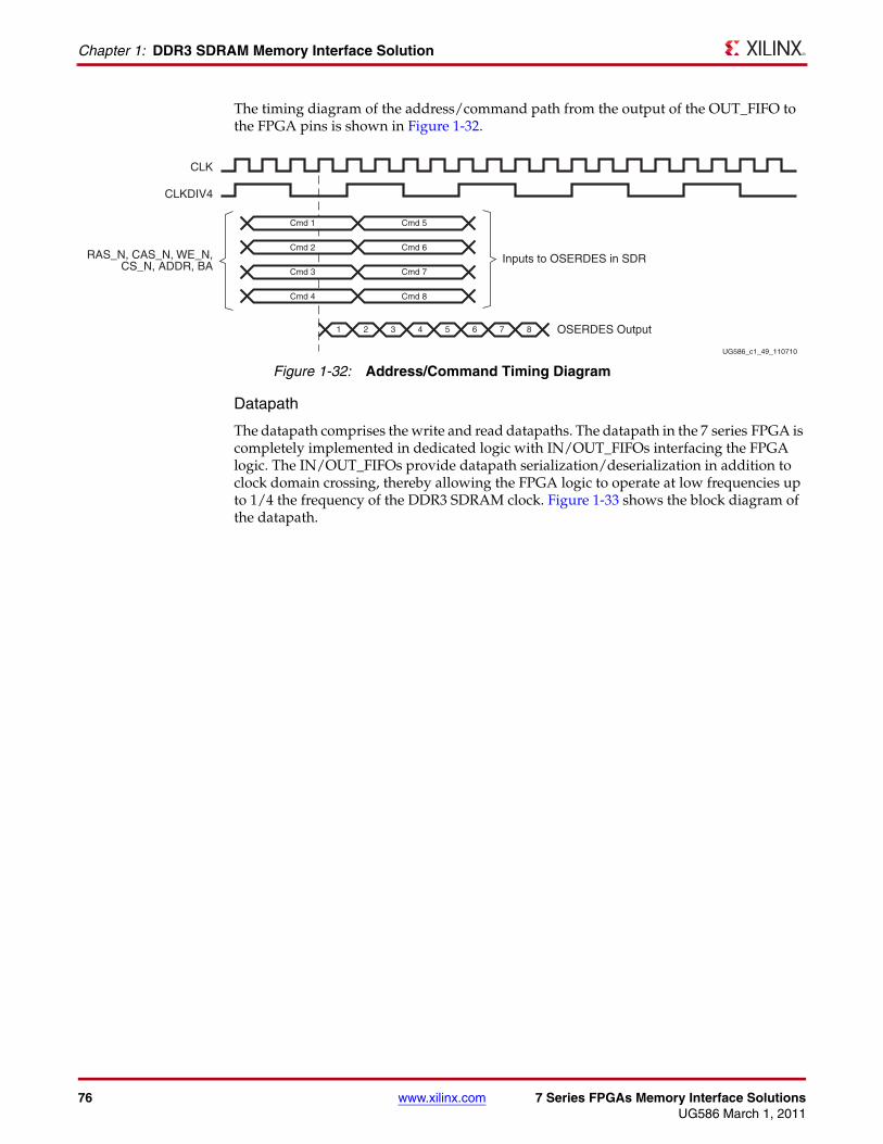
76 www.xilinx.com 7 Series FPGAs Memory Interface SolutionsUG586 March 1, 2011
Chapter 1: DDR3 SDRAM Memory Interface Solution
The timing diagram of the address/command path from the output of the OUT_FIFO to the FPGA pins is shown in Figure 1-32.
Datapath
The datapath comprises the write and read datapaths. The datapath in the 7 series FPGA is completely implemented in dedicated logic with IN/OUT_FIFOs interfacing the FPGA logic. The IN/OUT_FIFOs provide datapath serialization/deserialization in addition to clock domain crossing, thereby allowing the FPGA logic to operate at low frequencies up to 1/4 the frequency of the DDR3 SDRAM clock. Figure 1-33 shows the block diagram of the datapath.
X-Ref Target - Figure 1-32
Figure 1-32: Address/Command Timing Diagram
UG586_c1_49_110710
CLK
CLKDIV4
Inputs to OSERDES in SDR
OSERDES Output
Cmd 1 Cmd 5
Cmd 2 Cmd 6
Cmd 3 Cmd 7
Cmd 4
1 2 3 4 5 6 7 8
Cmd 8
RAS_N, CAS_N, WE_N,CS_N, ADDR, BA
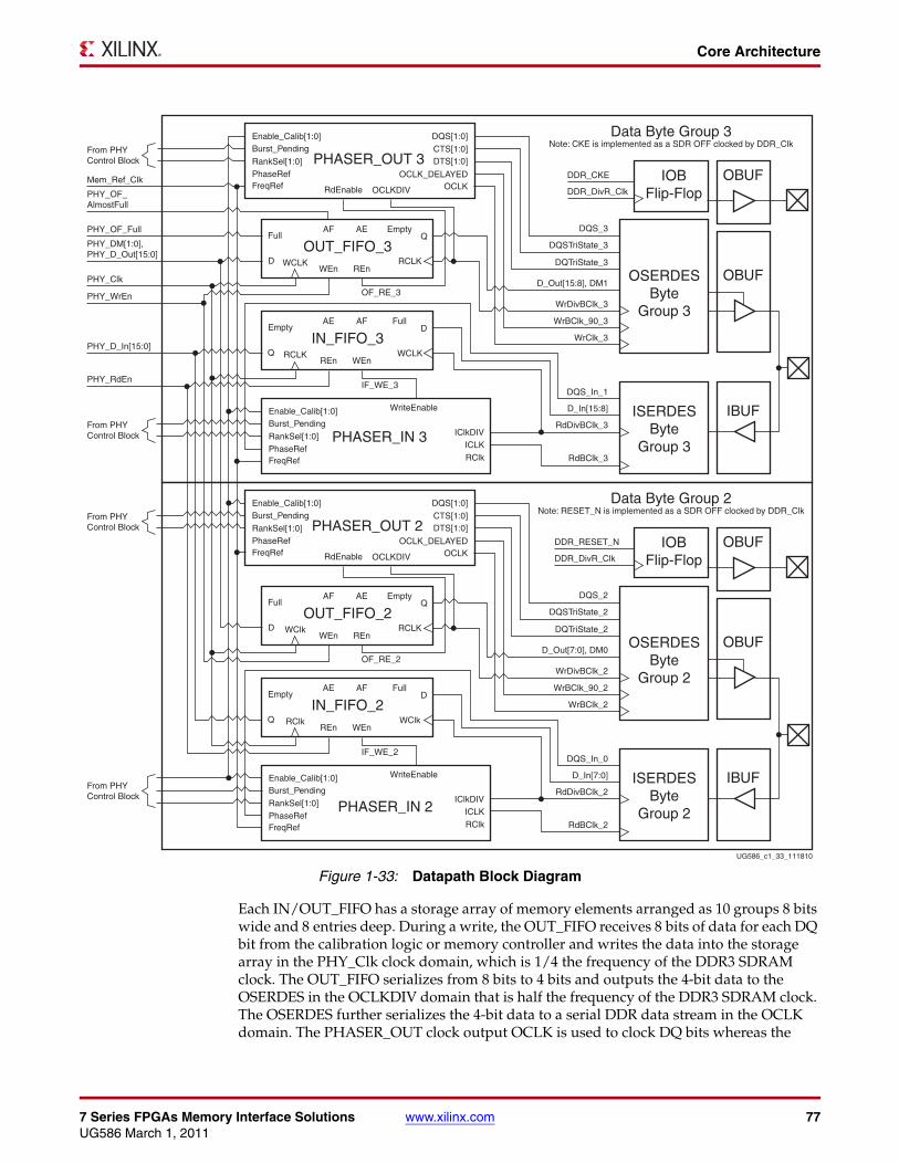
7 Series FPGAs Memory Interface Solutions www.xilinx.com 77UG586 March 1, 2011
Core Architecture
Each IN/OUT_FIFO has a storage array of memory elements arranged as 10 groups 8 bits wide and 8 entries deep. During a write, the OUT_FIFO receives 8 bits of data for each DQ bit from the calibration logic or memory controller and writes the data into the storage array in the PHY_Clk clock domain, which is 1/4 the frequency of the DDR3 SDRAM clock. The OUT_FIFO serializes from 8 bits to 4 bits and outputs the 4-bit data to the OSERDES in the OCLKDIV domain that is half the frequency of the DDR3 SDRAM clock. The OSERDES further serializes the 4-bit data to a serial DDR data stream in the OCLK domain. The PHASER_OUT clock output OCLK is used to clock DQ bits whereas the
X-Ref Target - Figure 1-33
Figure 1-33: Datapath Block Diagram
UG586_c1_33_111810
From PHYControl Block
Mem_Ref_ClkDDR_DivR_Clk
WrClk_3
DDR_CKE
PHY_OF_AlmostFull
PHY_OF_Full
PHY_Clk
OF_RE_3
IF_WE_3
PHY_WrEn
PHY_D_In[15:0]
PHY_RdEn
PHY_DM[1:0],PHY_D_Out[15:0]
Enable_Calib[1:0]Burst_PendingRankSel[1:0]
OCLKDIV
PhaseRefOCLK
OCLK_DELAYED
DQS[1:0]CTS[1:0]
FreqRef
DTS[1:0]PHASER_OUT 3
Data Byte Group 3Note: CKE is implemented as a SDR OFF clocked by DDR_Clk
D
FullAF AE Empty
WCLKWEn REn
WCLK
RCLK
QOUT_FIFO_3
Q
EmptyAE AF Full
RCLKREn WEn
DIN_FIFO_3
OSERDESByte
Group 3
OBUF
ISERDESByte
Group 3
IBUF
WrBClk_90_3
DQSTriState_3
DQTriState_3
DQS_3
DQS_In_1
D_In[15:8]
RdDivBClk_3
RdBClk_3
WrDivBClk_3
D_Out[15:8], DM1
IOBFlip-Flop
OBUF
From PHYControl Block
From PHYControl Block
From PHYControl Block
RdEnable
Enable_Calib[1:0]Burst_PendingRankSel[1:0] IClkDIV
PhaseRef ICLKRClkFreqRef
PHASER_IN 3
WriteEnable
DDR_DivR_Clk
WrBClk_2
DDR_RESET_N
OF_RE_2
IF_WE_2
Enable_Calib[1:0]Burst_PendingRankSel[1:0]
OCLKDIV
PhaseRefOCLK
OCLK_DELAYED
DQS[1:0]CTS[1:0]
FreqRef
DTS[1:0]PHASER_OUT 2
Data Byte Group 2Note: RESET_N is implemented as a SDR OFF clocked by DDR_Clk
D
FullAF AE Empty
WClkWEn REn
WClk
RCLK
QOUT_FIFO_2
Q
EmptyAE AF Full
RClkREn WEn
DIN_FIFO_2
OSERDESByte
Group 2
OBUF
ISERDESByte
Group 2
IBUF
WrBClk_90_2
DQSTriState_2
DQTriState_2
DQS_2
DQS_In_0
D_In[7:0]
RdDivBClk_2
RdBClk_2
WrDivBClk_2
D_Out[7:0], DM0
IOBFlip-Flop
OBUFRdEnable
Enable_Calib[1:0]Burst_PendingRankSel[1:0] IClkDIV
PhaseRef ICLKRClkFreqRef
PHASER_IN 2
WriteEnable
78 www.xilinx.com 7 Series FPGAs Memory Interface SolutionsUG586 March 1, 2011
Chapter 1: DDR3 SDRAM Memory Interface Solution
OCLK_DELAYED output is used to clock DQS to achieve the 90-degree phase offset between DQS and its associated DQ bits during writes. During write leveling, both OCLK and OCLK_DELAYED are shifted together to align DQS with CK at each DDR3 component.
The IN_FIFO shown in Figure 1-32 receives 4-bit data from each DQ bit ISERDES in a given byte group and writes them into the storage array. The IN_FIFO is used to further deserialize the data by writing two of the 4-bit datagrams into each 8-bit memory element. This 8-bit parallel data is output in the PHY_Clk clock domain which is 1/4 the frequency of the DDR3 SDRAM clock. Each read cycle from the IN_FIFO contains all the byte data read during a burst length 8 memory read transaction. The data bus width input to the dedicated PHY is 8X that of the DDR3 SDRAM when running the FPGA logic at 1/4 the frequency of the DDR3 SDRAM clock.
Calibration and Initialization Stages
Memory Initialization
The PHY executes a JEDEC-compliant DDR3 initialization sequence for memory following deassertion of system reset. Each DDR3 SDRAM has a series of mode registers, accessed via mode register set (MRS) commands. These mode registers determine various SDRAM behaviors, such as burst length, read and write CAS latency, and additive latency. The particular bit values programmed into these registers are configurable in the PHY and determined by the values of top-level HDL parameters like BURST_MODE (BL), BURST_TYPE, CAS latency (CL), CAS write latency (CWL), additive latency (AL), write recovery for auto precharge (tWR), on-die termination resistor values (RTT_NOM and RTT_WR), and output driver strength (OUTPUT_DRV).
Write Leveling
Write leveling, which is a feature available in DDR3 SDRAM, is performed in this stage of calibration. DDR3 SDRAM modules have adopted fly-by topology on clocks, address, commands, and control signals to improve signal integrity. Specifically, the clocks, address, and control signals are all routed in a daisy-chained fashion, and termination is located at the end of each trace. However, this causes a skew between the strobe (DQS) and the clock (CK) at each memory device on the module. Write leveling, a new feature in DDR3 SDRAMs, allows the controller to adjust each write DQS phase independently with respect to the CK forwarded to the DDR3 SDRAM device. This compensates for the skew between DQS and CK and meets the tDQSS specification. During write leveling, DQS is driven by the FPGA memory interface and DQ is driven by the DDR3 SDRAM device to provide feedback. The FPGA memory interface has the capability to delay DQS until a 0-to-1 transition is detected on DQ. Write leveling is performed once after power up. The calibration logic ORs the DQ bits in a byte to determine the transition because different memory vendors use different bits in a byte as feedback. The DQS delay can be achieved with the PHASER_OUT fine and coarse delay adjustment in the 7 series FPGAs. Figure 1-34 shows the write leveling block diagram.
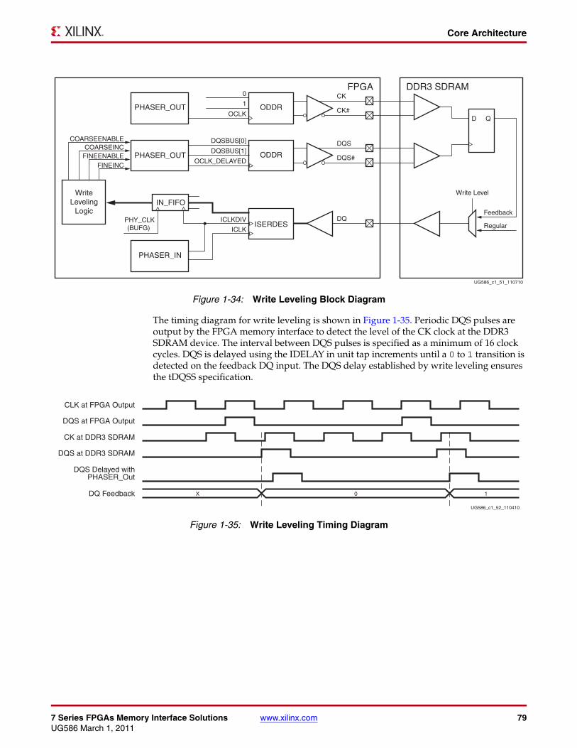
7 Series FPGAs Memory Interface Solutions www.xilinx.com 79UG586 March 1, 2011
Core Architecture
The timing diagram for write leveling is shown in Figure 1-35. Periodic DQS pulses are output by the FPGA memory interface to detect the level of the CK clock at the DDR3 SDRAM device. The interval between DQS pulses is specified as a minimum of 16 clock cycles. DQS is delayed using the IDELAY in unit tap increments until a 0 to 1 transition is detected on the feedback DQ input. The DQS delay established by write leveling ensures the tDQSS specification.
X-Ref Target - Figure 1-34
Figure 1-34: Write Leveling Block Diagram
DDR3 SDRAMFPGA0
1
D Q
CK
CK#
DQS
DQS#
ODDR
ODDR
Write Level
Regular
FeedbackDQ
ISERDES
IN_FIFO
PHASER_IN
PHASER_OUT
ICLK
ICLKDIV
PHASER_OUT
OCLK_DELAYED
DQSBUS[0]
DQSBUS[1]
OCLK
WriteLeveling
Logic
COARSEENABLECOARSEINC
FINEENABLEFINEINC
PHY_CLK(BUFG)
UG586_c1_51_110710
X-Ref Target - Figure 1-35
Figure 1-35: Write Leveling Timing Diagram
UG586_c1_52_110410
CLK at FPGA Output
DQS at FPGA Output
CK at DDR3 SDRAM
DQS at DDR3 SDRAM
DQ Feedback
DQS Delayed withPHASER_Out
0 1X
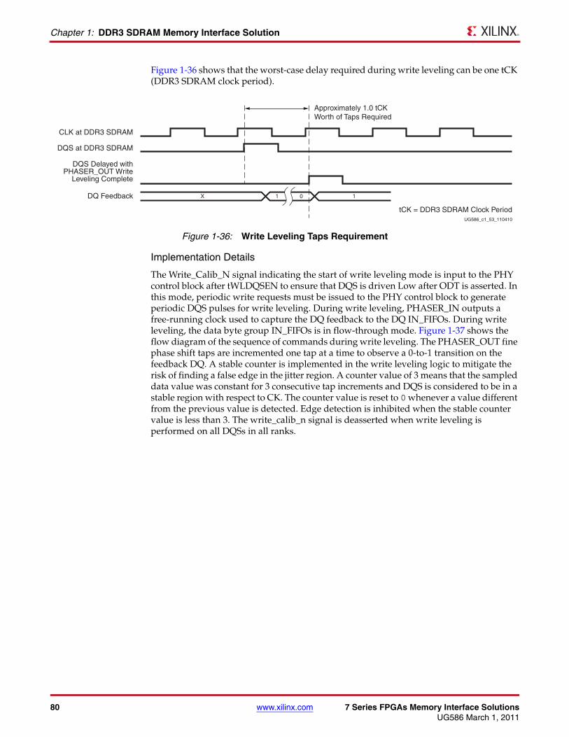
80 www.xilinx.com 7 Series FPGAs Memory Interface SolutionsUG586 March 1, 2011
Chapter 1: DDR3 SDRAM Memory Interface Solution
Figure 1-36 shows that the worst-case delay required during write leveling can be one tCK (DDR3 SDRAM clock period).
Implementation Details
The Write_Calib_N signal indicating the start of write leveling mode is input to the PHY control block after tWLDQSEN to ensure that DQS is driven Low after ODT is asserted. In this mode, periodic write requests must be issued to the PHY control block to generate periodic DQS pulses for write leveling. During write leveling, PHASER_IN outputs a free-running clock used to capture the DQ feedback to the DQ IN_FIFOs. During write leveling, the data byte group IN_FIFOs is in flow-through mode. Figure 1-37 shows the flow diagram of the sequence of commands during write leveling. The PHASER_OUT fine phase shift taps are incremented one tap at a time to observe a 0-to-1 transition on the feedback DQ. A stable counter is implemented in the write leveling logic to mitigate the risk of finding a false edge in the jitter region. A counter value of 3 means that the sampled data value was constant for 3 consecutive tap increments and DQS is considered to be in a stable region with respect to CK. The counter value is reset to 0 whenever a value different from the previous value is detected. Edge detection is inhibited when the stable counter value is less than 3. The write_calib_n signal is deasserted when write leveling is performed on all DQSs in all ranks.
X-Ref Target - Figure 1-36
Figure 1-36: Write Leveling Taps Requirement
UG586_c1_53_110410
CLK at DDR3 SDRAM
DQS at DDR3 SDRAM
DQS Delayed withPHASER_OUT Write
Leveling Complete
DQ Feedback 0 11X
Approximately 1.0 tCKWorth of Taps Required
tCK = DDR3 SDRAM Clock Period
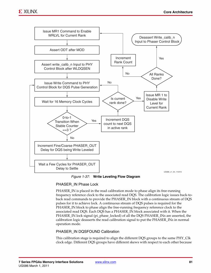
7 Series FPGAs Memory Interface Solutions www.xilinx.com 81UG586 March 1, 2011
Core Architecture
PHASER_IN Phase Lock
PHASER_IN is placed in the read calibration mode to phase align its free-running frequency reference clock to the associated read DQS. The calibration logic issues back-to-back read commands to provide the PHASER_IN block with a continuous stream of DQS pulses for it to achieve lock. A continuous stream of DQS pulses is required for the PHASER_IN block to phase align the free-running frequency reference clock to the associated read DQS. Each DQS has a PHASER_IN block associated with it. When the PHASER_IN lock signal (pi_phase_locked) of all the DQS PHASER_INs are asserted, the calibration logic deasserts the read calibration signal to put the PHASER_INs in normal operation mode.
PHASER_IN DQSFOUND Calibration
This calibration stage is required to align the different DQS groups to the same PHY_Clk clock edge. Different DQS groups have different skews with respect to each other because
X-Ref Target - Figure 1-37
Figure 1-37: Write Leveling Flow Diagram
UG586_c1_54_110410
No
No
No
Yes
Is currentrank done?
Increment DQScount to next DQS
in active rank
Issue MR 1 toDisable Write
Level forCurrent Rank
IncrementRank Count
Deassert Write_calib_nInput to Phaser Control Block
Issue MR1 Command to EnableWRLVL for Current Rank
Assert write_calib_n Input to PHYControl Block after WLDQSEN
Yes
Yes
Issue Write Command to PHYControl Block for DQS Pulse Generation
Increment Fine/Coarse PHASER_OUTDelay for DQS being Write Leveled
Wait a Few Cycles for PHASER_OUTDelay to Settle
Assert ODT after MOD
Wait for 16 Memory Clock Cycles
All RanksDone?
0-to-1Transition WhenStable Counter
==3 ?

82 www.xilinx.com 7 Series FPGAs Memory Interface SolutionsUG586 March 1, 2011
Chapter 1: DDR3 SDRAM Memory Interface Solution
of clock (CK) fly-by routing differences to each DDR3 component, and delay differences in each component. This calibration stage is required to determine the optimal position of read data_offset with respect to the read command for the entire interface.
In this stage of calibration, the PHASER_IN block is in normal operation mode and the calibration logic issues a set of four back-to-back read commands with gaps in between. The data_offset associated with the first read command is not accurate because the round-trip delays are unknown. The data_offset for the first set of read commands is set to CL+7. The data_offset value for the subsequent set of reads is decremented one memory clock cycle at a time until the DQSFOUND output from the PHASER_IN block is asserted. When the DQSFOUND signal is asserted for all the bytes, this calibration stage is complete.
Each byte group can be read out of the IN_FIFO on different PHY_Clk cycles due to fly-by routing differences and delay differences within each group. Therefore, the IN_FIFO Not Empty flags for all the byte groups are ANDed together and used as the read enable for all data IN_FIFOs. Figure 1-38 shows the read data capture timing diagram.
Read Leveling
Read leveling stage 1 is required to center align the read strobe in the read valid data window for the first stage of capture. In strobe-based memory interfaces like DDR3 SDRAM, the second stage transfer requires an additional pulse which in 7 series FPGAs is provided by the PHASER_IN block. This stage of calibration uses the PHASER_IN stage 2 fine delay line to center the capture clock in the valid DQ window. The capture clock is the free-running FREQ_REF clock that is phase aligned to read DQS in the PHASER_IN phase locked stage. A PHASER_IN provides two clock outputs namely ICLK and ICLKDIV. ICLK is the stage 2 delay output and ICLKDIV is the rising edge aligned divided by 2 version of ICLK.
X-Ref Target - Figure 1-38
Figure 1-38: Read Data Capture Timing Diagram
DQS Centered inValid Data Window
RdBCLK
Q2 Input
Q1 Input
Q4 Input
Q3 Input
ISERDES Q4 Output
ISERDES Q3 Output
ISERDES Q2 Output
ISERDES Q1 Output
RdDivBCLK
1 3 5 7
2 4 6 8
1 3 5 7
2 4 6 8
1 3 5 7
1 5
2 6
3 7
4 8
2 4 6 8
1 2 3 4 5 6 7 8
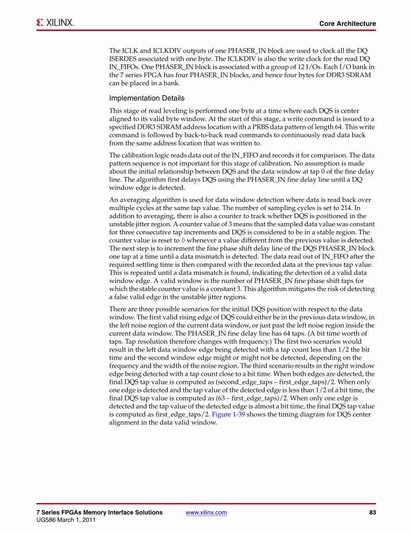
7 Series FPGAs Memory Interface Solutions www.xilinx.com 83UG586 March 1, 2011
Core Architecture
The ICLK and ICLKDIV outputs of one PHASER_IN block are used to clock all the DQ ISERDES associated with one byte. The ICLKDIV is also the write clock for the read DQ IN_FIFOs. One PHASER_IN block is associated with a group of 12 I/Os. Each I/O bank in the 7 series FPGA has four PHASER_IN blocks, and hence four bytes for DDR3 SDRAM can be placed in a bank.
Implementation Details
This stage of read leveling is performed one byte at a time where each DQS is center aligned to its valid byte window. At the start of this stage, a write command is issued to a specified DDR3 SDRAM address location with a PRBS data pattern of length 64. This write command is followed by back-to-back read commands to continuously read data back from the same address location that was written to.
The calibration logic reads data out of the IN_FIFO and records it for comparison. The data pattern sequence is not important for this stage of calibration. No assumption is made about the initial relationship between DQS and the data window at tap 0 of the fine delay line. The algorithm first delays DQS using the PHASER_IN fine delay line until a DQ window edge is detected.
An averaging algorithm is used for data window detection where data is read back over multiple cycles at the same tap value. The number of sampling cycles is set to 214. In addition to averaging, there is also a counter to track whether DQS is positioned in the unstable jitter region. A counter value of 3 means that the sampled data value was constant for three consecutive tap increments and DQS is considered to be in a stable region. The counter value is reset to 0 whenever a value different from the previous value is detected. The next step is to increment the fine phase shift delay line of the DQS PHASER_IN block one tap at a time until a data mismatch is detected. The data read out of IN_FIFO after the required settling time is then compared with the recorded data at the previous tap value. This is repeated until a data mismatch is found, indicating the detection of a valid data window edge. A valid window is the number of PHASER_IN fine phase shift taps for which the stable counter value is a constant 3. This algorithm mitigates the risk of detecting a false valid edge in the unstable jitter regions.
There are three possible scenarios for the initial DQS position with respect to the data window. The first valid rising edge of DQS could either be in the previous data window, in the left noise region of the current data window, or just past the left noise region inside the current data window. The PHASER_IN fine delay line has 64 taps. (A bit time worth of taps. Tap resolution therefore changes with frequency.) The first two scenarios would result in the left data window edge being detected with a tap count less than 1/2 the bit time and the second window edge might or might not be detected, depending on the frequency and the width of the noise region. The third scenario results in the right window edge being detected with a tap count close to a bit time. When both edges are detected, the final DQS tap value is computed as (second_edge_taps – first_edge_taps)/2. When only one edge is detected and the tap value of the detected edge is less than 1/2 of a bit time, the final DQS tap value is computed as (63 – first_edge_taps)/2. When only one edge is detected and the tap value of the detected edge is almost a bit time, the final DQS tap value is computed as first_edge_taps/2. Figure 1-39 shows the timing diagram for DQS center alignment in the data valid window.
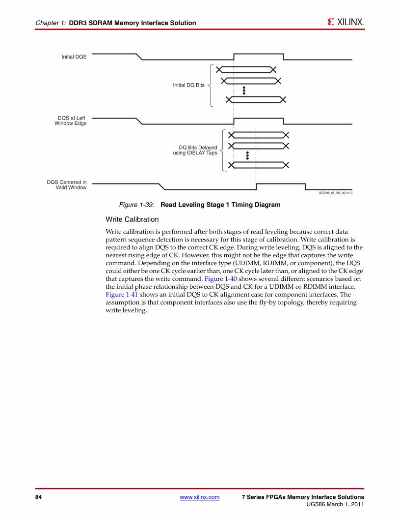
84 www.xilinx.com 7 Series FPGAs Memory Interface SolutionsUG586 March 1, 2011
Chapter 1: DDR3 SDRAM Memory Interface Solution
Write Calibration
Write calibration is performed after both stages of read leveling because correct data pattern sequence detection is necessary for this stage of calibration. Write calibration is required to align DQS to the correct CK edge. During write leveling, DQS is aligned to the nearest rising edge of CK. However, this might not be the edge that captures the write command. Depending on the interface type (UDIMM, RDIMM, or component), the DQS could either be one CK cycle earlier than, one CK cycle later than, or aligned to the CK edge that captures the write command. Figure 1-40 shows several different scenarios based on the initial phase relationship between DQS and CK for a UDIMM or RDIMM interface. Figure 1-41 shows an initial DQS to CK alignment case for component interfaces. The assumption is that component interfaces also use the fly-by topology, thereby requiring write leveling.
X-Ref Target - Figure 1-39
Figure 1-39: Read Leveling Stage 1 Timing Diagram
UG586_c1_55_091410
Initial DQS
DQS at Left Window Edge
DQS Centered inValid Window
DQ Bits Delayedusing IDELAY Taps
Initial DQ Bits
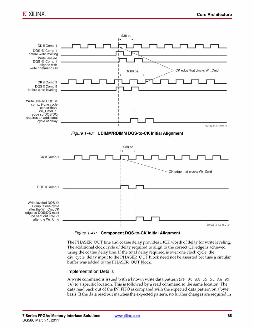
7 Series FPGAs Memory Interface Solutions www.xilinx.com 85UG586 March 1, 2011
Core Architecture
The PHASER_OUT fine and coarse delay provides 1 tCK worth of delay for write leveling. The additional clock cycle of delay required to align to the correct CK edge is achieved using the coarse delay line. If the total delay required is over one clock cycle, the div_cycle_delay input to the PHASER_OUT block need not be asserted because a circular buffer was added to the PHASER_OUT block.
Implementation Details
A write command is issued with a known write data pattern (FF 00 AA 55 55 AA 99 66) to a specific location. This is followed by a read command to the same location. The data read back out of the IN_FIFO is compared with the expected data pattern on a byte basis. If the data read out matches the expected pattern, no further changes are required in
X-Ref Target - Figure 1-40
Figure 1-40: UDIMM/RDIMM DQS-to-CK Initial Alignment
UG586_c1_57_110510
Write leveled DQS @comp. 9 one cycle
earlier than Wr_CmdCK
edge so DQS/DQrequires an additional
cycle of delay
938 ps
1600 ps CK edge that clocks Wr_Cmd
DQS @ Comp 1 before write leveling
Write leveled DQS @ Comp 1
aligned with write command CK
[email protected]@Comp.9
before write leveling
X-Ref Target - Figure 1-41
Figure 1-41: Component DQS-to-CK Initial Alignment
UG586_c1_58_091410
Write leveled DQS @Comp. 1 one cycle
after the Wr_CmdCKedge so DQS/DQ must
be sent out CWL-1after the Wr_Cmd
938 ps
CK edge that clocks Wr_Cmd
86 www.xilinx.com 7 Series FPGAs Memory Interface SolutionsUG586 March 1, 2011
Chapter 1: DDR3 SDRAM Memory Interface Solution
the write path for that byte, as shown in Figure 1-42. If the first two data words read back match the second set of data words in the expected pattern, the DQS and DQ 3-state signal must be delayed by one memory clock. This scenario is shown in Figure 1-43. After all the bytes are calibrated, the calibration logic asserts the init_calib_complete signal indicating the completion of the initialization and calibration sequence. The memory controller can now drive the address, command, and data buses.
Memory Controller to PHY Interface
The calibration logic module constructs the PHY control word before sending it to the PHY control block during calibration. After calibration is complete, the init_calib_complete signal is asserted and sent to the memory controller to indicate that normal operation can begin. To avoid latency increase, the memory controller must send commands in the format required by the dedicated PHY block. As a result, the address, command, control, and data buses are multiplexed before being sent to the PHY control block. These buses are driven by the calibration module during the memory initialization and calibration stages and by the memory controller during normal operation. Table 1-25 describes the memory controller to PHY interface signals. These signals are synchronous to the fabric clock.
X-Ref Target - Figure 1-42
Figure 1-42: DQS Aligned to the Correct CK Edge - No Change in Write Path
UG586_c1_59_091410
Write [email protected]
aligned to theWr_Cmd CK edge
FF 00 AA AA 99 6655 55
CLW = 9CK edge that clocks Wr_Cmd
X-Ref Target - Figure 1-43
Figure 1-43: DQS Aligned to Incorrect CK Edge - Delay DQS/DQ by One Memory Clock Cycle
UG586_c1_60_091410
Write [email protected]
one cycle earlier thanWr_Cmd CK edge
[email protected] be delayed by
1 memory clock cycle
FF 00 AA AA 99 6655 55
CWL = 9CK edge that clocks Wr_Cmd
7 Series FPGAs Memory Interface Solutions www.xilinx.com 87UG586 March 1, 2011
Core Architecture
Table 1-25: Memory Controller to Calibration Logic Interface Signals
Signal Name WidthI/O To/From
PHYType Description
rst 1 Input The rstdiv0 output from the infrastructure module synchronized to the PHY_Clk domain.
PHY_Clk 1 Input This clock signal is 1/4 the frequency of the DDR3 clock.
mem_refclk 1 Input This is the DDR3 frequency clock.
freq_refclk 1 Input This signal is the same frequency as mem_refclk between 400 MHz to 1066 MHz, and 1/2 or 1/4 of mem_refclk for frequencies below 400 MHz.
sync_pulse 1 Input This is the synchronization pulse output by the PLL.
pll_lock 1 Input The LOCKED output of the PLL instantiated in the infrastructure module.
mc_ras_n [nCK_PER_CLK0 – 1:0] Input Active Low
mc_xxx_n[0] is the first cmd in the sequence of four.
mc_cas_n [nCK_PER_CLK – 1:0] Input Active Low
mc_xxx_n[0] is the first cmd in the sequence of four.
mc_we_n [nCK_PER_CLK – 1:0] Input Active Low
mc_xxx_n[0] is the first cmd in the sequence of four.
mc_address [ROW_WIDTH × nCK_PER_CLK – 1:0]
Input mc_address[ROW_WIDTH – 1:0] is the first command address in the sequence of four.
mc_bank [BANK_WIDTH × nCK_PER_CLK – 1:0]
Input mc_bank[BANK_WIDTH – 1:0] is the first command bank address in the sequence of four.
mc_cs_n [CS_WIDTH × nCS_PER_RANK ×
nCK_PER_CLK – 1:0]
Input mc_cs_n [CS_WIDTH – 1:0] is the cs_n associated with the first command in the sequence.
mc_reset_n 1 Input Active Low
mc_reset_n is input directly to the IOLOGIC without an OUT_FIFO.
mc_wrdata [2 × nCK_PER_CLK × DQ_WIDTH – 1:0]
Input This is the write data to the dedicated PHY. It is 8x the memory DQ width for a 4:1 clock ratio.
mc_wrdata_mask [2 × nCK_PER_CLK × (DQ_WIDTH/8) – 1:0]
Input This is the write data mask to the dedicated PHY. It is 8x the memory DM width for a 4:1 clock ratio.
mc_wrdata_en 1 Input Active High
This signal is the WREN input to the DQ OUT_FIFO.
mc_cmd_wren 1 Input Active Low
This signal is the write enable input of the address/command OUT_FIFOs.
88 www.xilinx.com 7 Series FPGAs Memory Interface SolutionsUG586 March 1, 2011
Chapter 1: DDR3 SDRAM Memory Interface Solution
mc_ctl_wren 1 Input Active Low
This signal is the write enable input to the PHY control word FIFO in the dedicated PHY block.
mc_cmd [2:0] Input This signal is used for PHY_Ctl_Wd configuration:
0x04: Non-data command (No column command in the sequence of commands)0x01: Write command0x03: Read command
mc_data_offset [5:0] Input This signal is used for PHY_Ctl_Wd configuration:
0x00: Non-data command (No column command in the sequence of commands)CWL + COL cmd position: Write commandcalib_rd_data_offset+COL cmd position – 1: Read command
mc_aux_out0 [3:0] Input Active High
This is the auxiliary outputs field in the PHY control word used to control ODT and CKE assertion.
mc_aux_out1 [3:0] Input Active High
This is the auxiliary outputs field in the PHY control word used to control ODT and CKE assertion for four-rank interfaces.
mc_rank_cnt [1:0] Input This is the rank accessed by the command sequence in the PHY control word.
phy_rd_data [2 × nCK_PER_CLK × DQ_WIDTH – 1:0]
Output This is the read data from the dedicated PHY. It is 8x the memory DQ width for a 4:1 clock ratio.
phy_rddata_valid 1 Output Active High
This signal is asserted when valid read data is available.
calib_rd_data_offset [6 × RANKS – 1:0] Output This signal is the calibrated read data offset value with respect to command 0 in the sequence of four commands.
init_calib_complete 1 Output Active High
This signal is asserted after memory initialization and calibration are completed.
Notes: 1. The parameter nCK_PER_CLK defines the number of DDR3 SDRAM clock cycles per PHY_Clk cycle.2. The parameter ROW_WIDTH is the number of DDR3 SDRAM ranks.3. The parameter BANK_WIDTH is the number of DDR3 SDRAM banks.4. The parameter CS_WIDTH is the number of DDR3 SDRAM cs_n signals.5. The parameter CKE_WIDTH is the number of DDR3 SDRAM CKE signals.6. The parameter DQ_WIDTH is the width of the DDR3 SDRAM DQ bus.
Table 1-25: Memory Controller to Calibration Logic Interface Signals (Cont’d)
Signal Name WidthI/O To/From
PHYType Description
7 Series FPGAs Memory Interface Solutions www.xilinx.com 89UG586 March 1, 2011
Designing with the Core
Designing with the CoreThe core is bundled with an example design that can be simulated. The example design can be used as a starting point for the user design or as a reference for debugging purposes.
Only supported modifications should be made to the configuration of the core. See Customizing the Core, page 97 for supported configuration parameters.
Interfacing to the CoreThe memory controller can be connected using either the AXI4 slave interface, the UI, or the native interface. The AXI4 slave interface provides an AXI4 memory-mapped compliant slave ideal for connecting to processor subsystems. The AXI4 slave interface converts its transactions to pass them over the UI. The UI resembles a simple FIFO interface and always returns the data in order. The native interface offers higher performance in some situations, but is more challenging to use.
The native interface contains no buffers and returns data as soon as possible, but the return data might be out of order. The application must reorder the received data internally if the native interface is used and reordering is enabled. The following sections describe timing protocols of each interface and how they should be controlled.
AXI4 Slave InterfaceThe AXI4 slave interface follows the AXI4 memory-mapped slave protocol specification as described in the ARM AMBA open specifications. See this specification [Ref 2] for the signaling details of the AXI4 slave interface.
AXI addressingThe AXI address from the AXI master is a true byte address. The address at the user interface of the memory controller is normalized to the data width of the external memory. The AXI shim normalizes the address from the AXI master to the memory data width based on the AXSIZE. The address at the input of the memory controller user interface from the AXI shim can be configured in two modes; see the User Interface section for more details.
User InterfaceThe mapping between the User Interface address bus and the physical memory row, bank and column can be configured. Depending on how the application data is organized, addressing scheme Bank- Row-Column or Row-Bank-Column can be chosen to optimize controller efficiency. These addressing schemes are shown in Figure 1-44 and Figure 1-45.
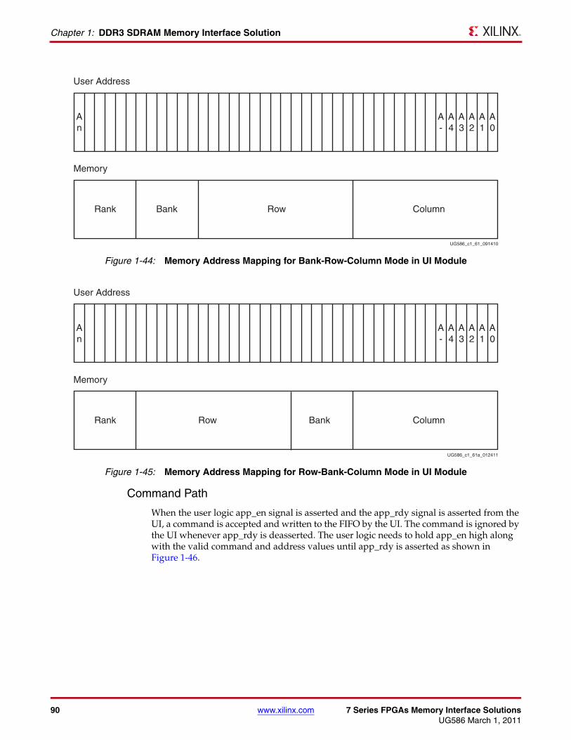
90 www.xilinx.com 7 Series FPGAs Memory Interface SolutionsUG586 March 1, 2011
Chapter 1: DDR3 SDRAM Memory Interface Solution
Command Path
When the user logic app_en signal is asserted and the app_rdy signal is asserted from the UI, a command is accepted and written to the FIFO by the UI. The command is ignored by the UI whenever app_rdy is deasserted. The user logic needs to hold app_en high along with the valid command and address values until app_rdy is asserted as shown in Figure 1-46.
X-Ref Target - Figure 1-44
Figure 1-44: Memory Address Mapping for Bank-Row-Column Mode in UI Module
User Address
An
A0
A1
A2
A3
A4
A-
Memory
Rank Bank Row Column
UG586_c1_61_091410
X-Ref Target - Figure 1-45
Figure 1-45: Memory Address Mapping for Row-Bank-Column Mode in UI Module
User Address
An
A0
A1
A2
A3
A4
A-
Memory
Rank Row Bank Column
UG586_c1_61a_012411
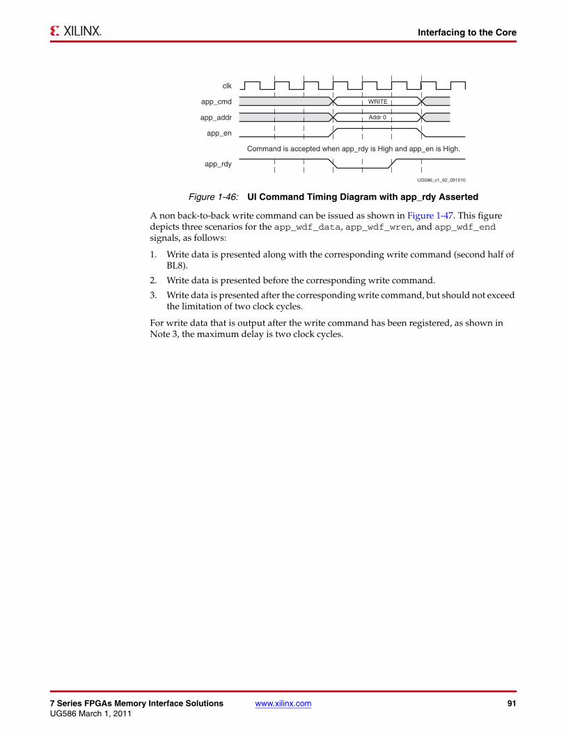
7 Series FPGAs Memory Interface Solutions www.xilinx.com 91UG586 March 1, 2011
Interfacing to the Core
A non back-to-back write command can be issued as shown in Figure 1-47. This figure depicts three scenarios for the app_wdf_data, app_wdf_wren, and app_wdf_end signals, as follows:
1. Write data is presented along with the corresponding write command (second half of BL8).
2. Write data is presented before the corresponding write command.
3. Write data is presented after the corresponding write command, but should not exceed the limitation of two clock cycles.
For write data that is output after the write command has been registered, as shown in Note 3, the maximum delay is two clock cycles.
X-Ref Target - Figure 1-46
Figure 1-46: UI Command Timing Diagram with app_rdy Asserted
UG586_c1_62_091510
clk
app_cmd WRITE
app_addr Addr 0
app_en
app_rdy
Command is accepted when app_rdy is High and app_en is High.
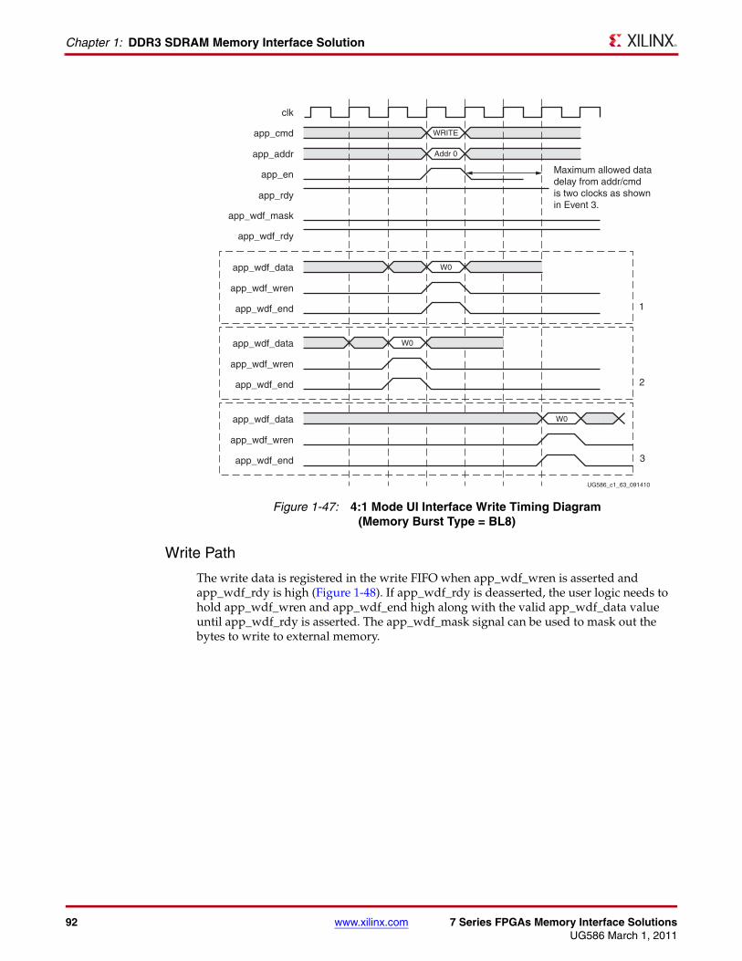
92 www.xilinx.com 7 Series FPGAs Memory Interface SolutionsUG586 March 1, 2011
Chapter 1: DDR3 SDRAM Memory Interface Solution
Write Path
The write data is registered in the write FIFO when app_wdf_wren is asserted and app_wdf_rdy is high (Figure 1-48). If app_wdf_rdy is deasserted, the user logic needs to hold app_wdf_wren and app_wdf_end high along with the valid app_wdf_data value until app_wdf_rdy is asserted. The app_wdf_mask signal can be used to mask out the bytes to write to external memory.
X-Ref Target - Figure 1-47
Figure 1-47: 4:1 Mode UI Interface Write Timing Diagram (Memory Burst Type = BL8)
UG586_c1_63_091410
app_wdf_data
clk
app_cmd WRITE
app_addr Addr 0
app_wdf_end
app_en
app_wdf_wren
app_rdy
app_wdf_mask
app_wdf_rdy
W0
W0app_wdf_data
app_wdf_end
app_wdf_wren
app_wdf_data
app_wdf_end
app_wdf_wren
W0
Maximum allowed data delay from addr/cmd is two clocks as shown in Event 3.
1
2
3
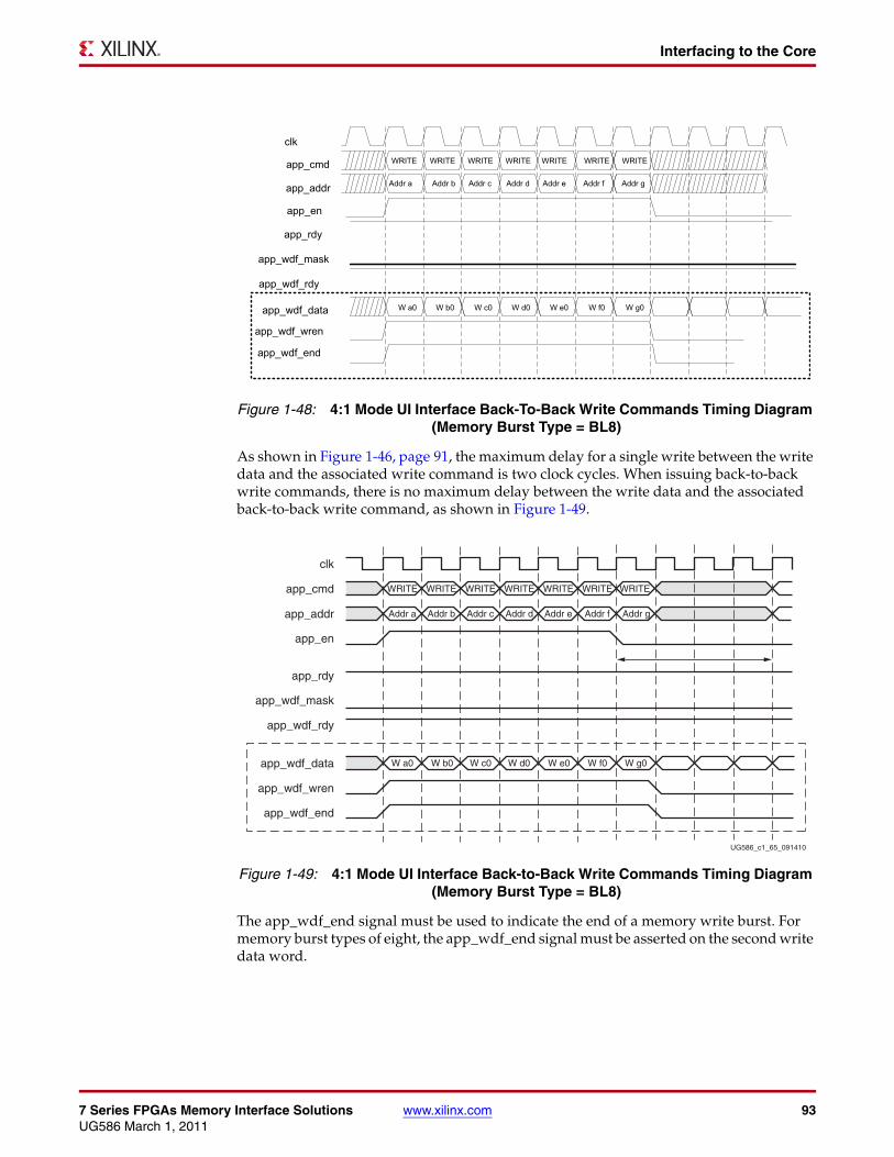
7 Series FPGAs Memory Interface Solutions www.xilinx.com 93UG586 March 1, 2011
Interfacing to the Core
As shown in Figure 1-46, page 91, the maximum delay for a single write between the write data and the associated write command is two clock cycles. When issuing back-to-back write commands, there is no maximum delay between the write data and the associated back-to-back write command, as shown in Figure 1-49.
The app_wdf_end signal must be used to indicate the end of a memory write burst. For memory burst types of eight, the app_wdf_end signal must be asserted on the second write data word.
X-Ref Target - Figure 1-48
Figure 1-48: 4:1 Mode UI Interface Back-To-Back Write Commands Timing Diagram (Memory Burst Type = BL8)
X-Ref Target - Figure 1-49
Figure 1-49: 4:1 Mode UI Interface Back-to-Back Write Commands Timing Diagram (Memory Burst Type = BL8)
��"
�������
���� �����"
���� ������
������ !�#$%
�������� ������
�����
���� ��� ��
���� �����
���� ������� !��� !�&� !��� !��� !��� !��� !���
!�#$% !�#$% !�#$% !�#$%
�����& ������ ������ ������
!�#$%
������
!�#$%
������
UG586_c1_65_091410
app_wdf_data
clk
app_cmd
W a0
WRITE WRITE WRITE WRITE WRITE WRITE WRITE
app_addr Addr a Addr b Addr c Addr d Addr e Addr f Addr g
app_wdf_end
app_en
app_wdf_wren
app_rdy
app_wdf_mask
app_wdf_rdy
W b0 W c0 W d0 W e0 W f0 W g0
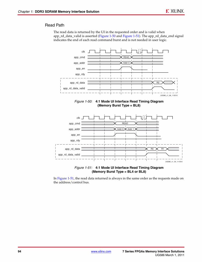
94 www.xilinx.com 7 Series FPGAs Memory Interface SolutionsUG586 March 1, 2011
Chapter 1: DDR3 SDRAM Memory Interface Solution
Read Path
The read data is returned by the UI in the requested order and is valid when app_rd_data_valid is asserted (Figure 1-50 and Figure 1-51). The app_rd_data_end signal indicates the end of each read command burst and is not needed in user logic.
In Figure 1-51, the read data returned is always in the same order as the requests made on the address/control bus.
X-Ref Target - Figure 1-50
Figure 1-50: 4:1 Mode UI Interface Read Timing Diagram(Memory Burst Type = BL8)
X-Ref Target - Figure 1-51
Figure 1-51: 4:1 Mode UI Interface Read Timing Diagram(Memory Burst Type = BL4 or BL8)
UG586_c1_66_110510
app_rd_data
clk
app_cmd
R0
READ
app_addr Addr 0
app_en
app_rd_data_valid
app_rdy
UG586_c1_50_111810
app_rd_data
clk
app_cmd
R0
app_addr Addr 1
app_en
app_rd_data_valid
app_rdy
Addr 0
R1
READ
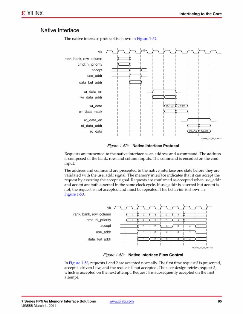
7 Series FPGAs Memory Interface Solutions www.xilinx.com 95UG586 March 1, 2011
Interfacing to the Core
Native InterfaceThe native interface protocol is shown in Figure 1-52.
Requests are presented to the native interface as an address and a command. The address is composed of the bank, row, and column inputs. The command is encoded on the cmd input.
The address and command are presented to the native interface one state before they are validated with the use_addr signal. The memory interface indicates that it can accept the request by asserting the accept signal. Requests are confirmed as accepted when use_addr and accept are both asserted in the same clock cycle. If use_addr is asserted but accept is not, the request is not accepted and must be repeated. This behavior is shown in Figure 1-53.
In Figure 1-53, requests 1 and 2 are accepted normally. The first time request 3 is presented, accept is driven Low, and the request is not accepted. The user design retries request 3, which is accepted on the next attempt. Request 4 is subsequently accepted on the first attempt.
X-Ref Target - Figure 1-52
Figure 1-52: Native Interface Protocol
X-Ref Target - Figure 1-53
Figure 1-53: Native Interface Flow Control
UG586_c1_67_110510
clk
rank, bank, row, column
cmd, hi_priority
accept
use_addr
data_buf_addr
wr_data_en
wr_data_addr
rd_data_en
rd_data_addr
rd_data
wr_data
wr_data_mask
D0–D3 D4–D7
D0–D3 D4–D7
clk
rank, bank, row, column
cmd, hi_priority
accept
use_addr
data_buf_addr
UG586_c1_68_091410
1 2 3 3 4
1 2 3 3 4
1 2 3 3 4
1 2 3 3 4
1 2 3 3 4
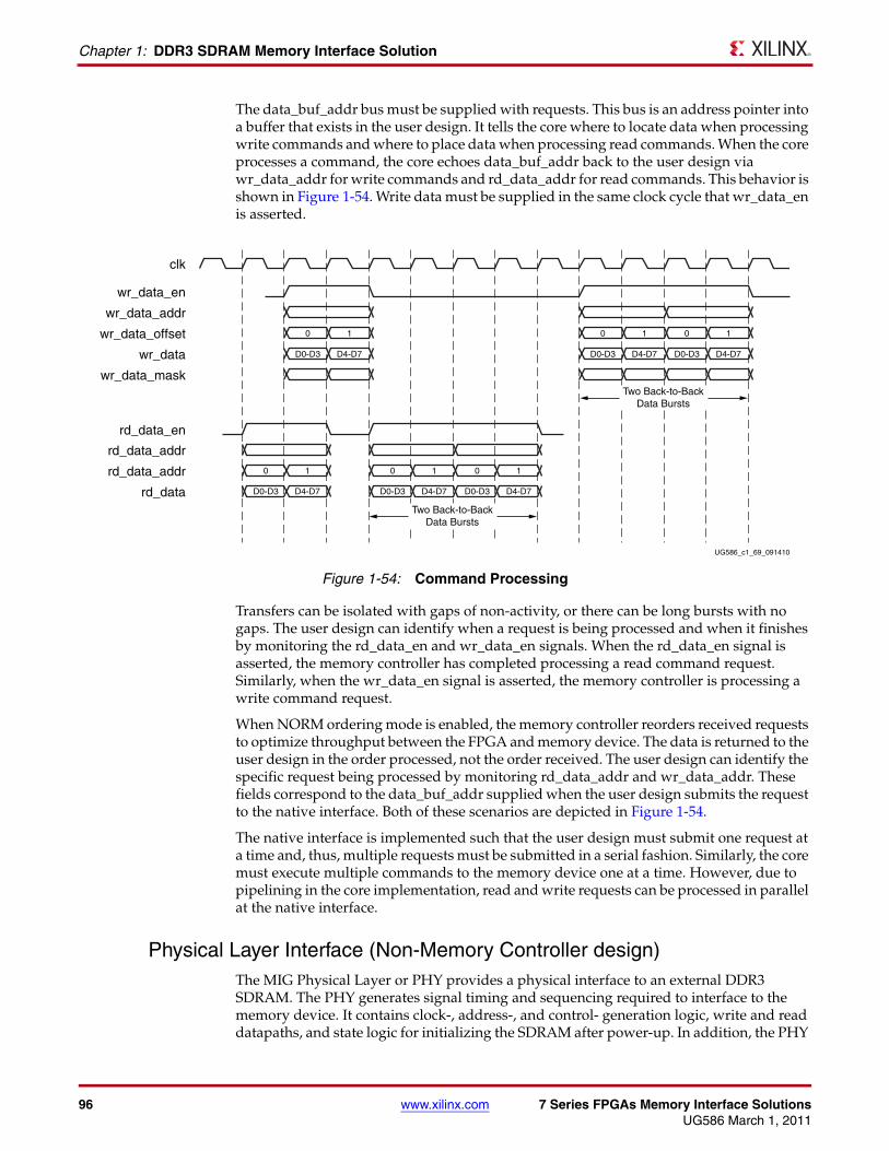
96 www.xilinx.com 7 Series FPGAs Memory Interface SolutionsUG586 March 1, 2011
Chapter 1: DDR3 SDRAM Memory Interface Solution
The data_buf_addr bus must be supplied with requests. This bus is an address pointer into a buffer that exists in the user design. It tells the core where to locate data when processing write commands and where to place data when processing read commands. When the core processes a command, the core echoes data_buf_addr back to the user design via wr_data_addr for write commands and rd_data_addr for read commands. This behavior is shown in Figure 1-54. Write data must be supplied in the same clock cycle that wr_data_en is asserted.
Transfers can be isolated with gaps of non-activity, or there can be long bursts with no gaps. The user design can identify when a request is being processed and when it finishes by monitoring the rd_data_en and wr_data_en signals. When the rd_data_en signal is asserted, the memory controller has completed processing a read command request. Similarly, when the wr_data_en signal is asserted, the memory controller is processing a write command request.
When NORM ordering mode is enabled, the memory controller reorders received requests to optimize throughput between the FPGA and memory device. The data is returned to the user design in the order processed, not the order received. The user design can identify the specific request being processed by monitoring rd_data_addr and wr_data_addr. These fields correspond to the data_buf_addr supplied when the user design submits the request to the native interface. Both of these scenarios are depicted in Figure 1-54.
The native interface is implemented such that the user design must submit one request at a time and, thus, multiple requests must be submitted in a serial fashion. Similarly, the core must execute multiple commands to the memory device one at a time. However, due to pipelining in the core implementation, read and write requests can be processed in parallel at the native interface.
Physical Layer Interface (Non-Memory Controller design)The MIG Physical Layer or PHY provides a physical interface to an external DDR3 SDRAM. The PHY generates signal timing and sequencing required to interface to the memory device. It contains clock-, address-, and control- generation logic, write and read datapaths, and state logic for initializing the SDRAM after power-up. In addition, the PHY
X-Ref Target - Figure 1-54
Figure 1-54: Command Processing
clk
wr_data_en
wr_data_addr
wr_data_offset
wr_data
wr_data_mask
rd_data_en
rd_data_addr
rd_data_addr
rd_data
0
D0-D3
0
D0-D3
1
D4-D7
0
D0-D3
1
D4-D7
0
D0-D3
1
D4-D7
0
D0-D3
1
D4-D7
1
D4-D7
0
Two Back-to-BackData Bursts
D0-D3
1
D4-D7
UG586_c1_69_091410
Two Back-to-BackData Bursts
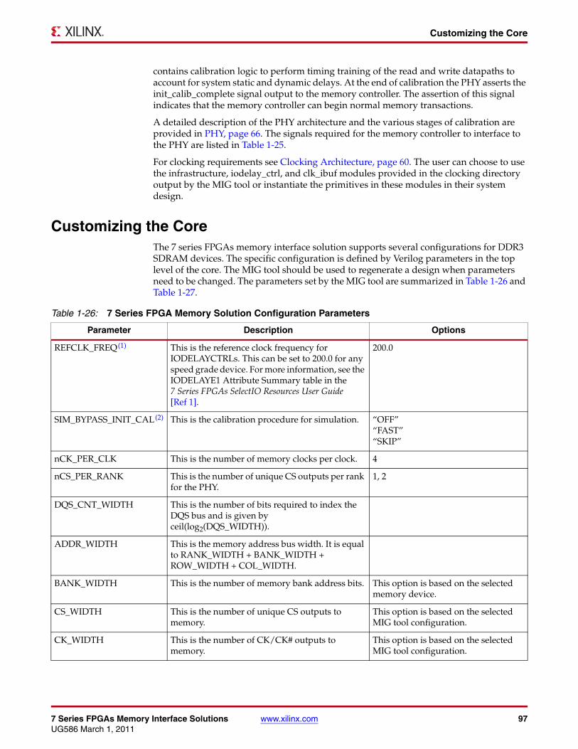
7 Series FPGAs Memory Interface Solutions www.xilinx.com 97UG586 March 1, 2011
Customizing the Core
contains calibration logic to perform timing training of the read and write datapaths to account for system static and dynamic delays. At the end of calibration the PHY asserts the init_calib_complete signal output to the memory controller. The assertion of this signal indicates that the memory controller can begin normal memory transactions.
A detailed description of the PHY architecture and the various stages of calibration are provided in PHY, page 66. The signals required for the memory controller to interface to the PHY are listed in Table 1-25.
For clocking requirements see Clocking Architecture, page 60. The user can choose to use the infrastructure, iodelay_ctrl, and clk_ibuf modules provided in the clocking directory output by the MIG tool or instantiate the primitives in these modules in their system design.
Customizing the CoreThe 7 series FPGAs memory interface solution supports several configurations for DDR3 SDRAM devices. The specific configuration is defined by Verilog parameters in the top level of the core. The MIG tool should be used to regenerate a design when parameters need to be changed. The parameters set by the MIG tool are summarized in Table 1-26 and Table 1-27.
Table 1-26: 7 Series FPGA Memory Solution Configuration Parameters
Parameter Description Options
REFCLK_FREQ(1) This is the reference clock frequency for IODELAYCTRLs. This can be set to 200.0 for any speed grade device. For more information, see the IODELAYE1 Attribute Summary table in the 7 Series FPGAs SelectIO Resources User Guide [Ref 1].
200.0
SIM_BYPASS_INIT_CAL(2) This is the calibration procedure for simulation. “OFF”“FAST”“SKIP”
nCK_PER_CLK This is the number of memory clocks per clock. 4
nCS_PER_RANK This is the number of unique CS outputs per rank for the PHY.
1, 2
DQS_CNT_WIDTH This is the number of bits required to index the DQS bus and is given by ceil(log2(DQS_WIDTH)).
ADDR_WIDTH This is the memory address bus width. It is equal to RANK_WIDTH + BANK_WIDTH + ROW_WIDTH + COL_WIDTH.
BANK_WIDTH This is the number of memory bank address bits. This option is based on the selected memory device.
CS_WIDTH This is the number of unique CS outputs to memory.
This option is based on the selected MIG tool configuration.
CK_WIDTH This is the number of CK/CK# outputs to memory.
This option is based on the selected MIG tool configuration.
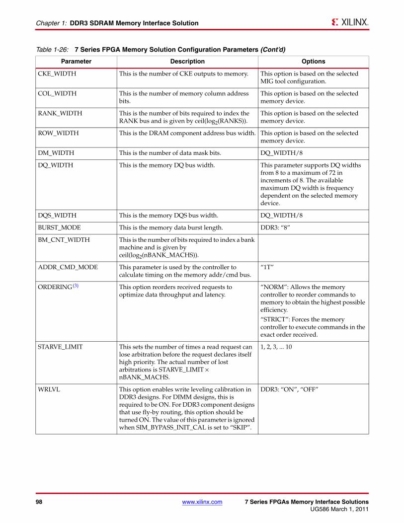
98 www.xilinx.com 7 Series FPGAs Memory Interface SolutionsUG586 March 1, 2011
Chapter 1: DDR3 SDRAM Memory Interface Solution
CKE_WIDTH This is the number of CKE outputs to memory. This option is based on the selected MIG tool configuration.
COL_WIDTH This is the number of memory column address bits.
This option is based on the selected memory device.
RANK_WIDTH This is the number of bits required to index the RANK bus and is given by ceil(log2(RANKS)).
This option is based on the selected memory device.
ROW_WIDTH This is the DRAM component address bus width. This option is based on the selected memory device.
DM_WIDTH This is the number of data mask bits. DQ_WIDTH/8
DQ_WIDTH This is the memory DQ bus width. This parameter supports DQ widths from 8 to a maximum of 72 in increments of 8. The available maximum DQ width is frequency dependent on the selected memory device.
DQS_WIDTH This is the memory DQS bus width. DQ_WIDTH/8
BURST_MODE This is the memory data burst length. DDR3: “8”
BM_CNT_WIDTH This is the number of bits required to index a bank machine and is given by ceil(log2(nBANK_MACHS)).
ADDR_CMD_MODE This parameter is used by the controller to calculate timing on the memory addr/cmd bus.
“1T”
ORDERING(3) This option reorders received requests to optimize data throughput and latency.
“NORM”: Allows the memory controller to reorder commands to memory to obtain the highest possible efficiency.
“STRICT”: Forces the memory controller to execute commands in the exact order received.
STARVE_LIMIT This sets the number of times a read request can lose arbitration before the request declares itself high priority. The actual number of lost arbitrations is STARVE_LIMIT × nBANK_MACHS.
1, 2, 3, ... 10
WRLVL This option enables write leveling calibration in DDR3 designs. For DIMM designs, this is required to be ON. For DDR3 component designs that use fly-by routing, this option should be turned ON. The value of this parameter is ignored when SIM_BYPASS_INIT_CAL is set to “SKIP”.
DDR3: “ON”, “OFF”
Table 1-26: 7 Series FPGA Memory Solution Configuration Parameters (Cont’d)
Parameter Description Options
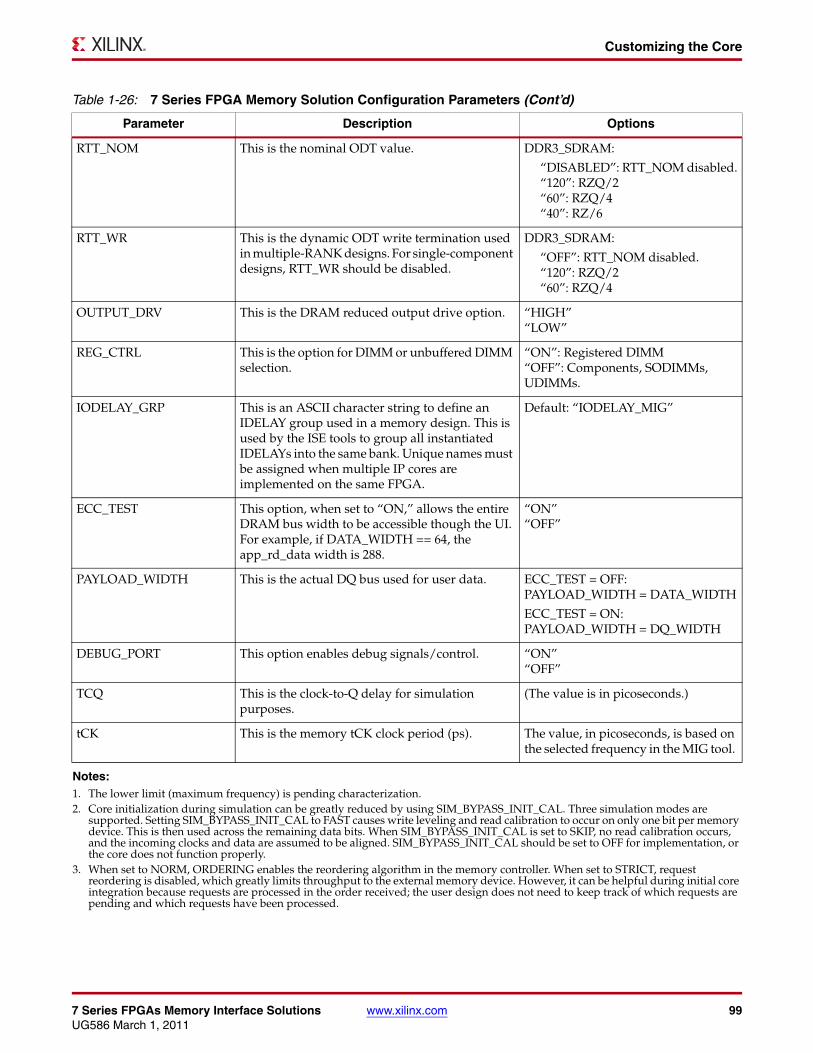
7 Series FPGAs Memory Interface Solutions www.xilinx.com 99UG586 March 1, 2011
Customizing the Core
RTT_NOM This is the nominal ODT value. DDR3_SDRAM:
“DISABLED”: RTT_NOM disabled.“120”: RZQ/2 “60”: RZQ/4 “40”: RZ/6
RTT_WR This is the dynamic ODT write termination used in multiple-RANK designs. For single-component designs, RTT_WR should be disabled.
DDR3_SDRAM:
“OFF”: RTT_NOM disabled. “120”: RZQ/2 “60”: RZQ/4
OUTPUT_DRV This is the DRAM reduced output drive option. “HIGH”“LOW”
REG_CTRL This is the option for DIMM or unbuffered DIMM selection.
“ON”: Registered DIMM“OFF”: Components, SODIMMs, UDIMMs.
IODELAY_GRP This is an ASCII character string to define an IDELAY group used in a memory design. This is used by the ISE tools to group all instantiated IDELAYs into the same bank. Unique names must be assigned when multiple IP cores are implemented on the same FPGA.
Default: “IODELAY_MIG”
ECC_TEST This option, when set to “ON,” allows the entire DRAM bus width to be accessible though the UI. For example, if DATA_WIDTH == 64, the app_rd_data width is 288.
“ON”“OFF”
PAYLOAD_WIDTH This is the actual DQ bus used for user data. ECC_TEST = OFF:PAYLOAD_WIDTH = DATA_WIDTH
ECC_TEST = ON:PAYLOAD_WIDTH = DQ_WIDTH
DEBUG_PORT This option enables debug signals/control. “ON”“OFF”
TCQ This is the clock-to-Q delay for simulation purposes.
(The value is in picoseconds.)
tCK This is the memory tCK clock period (ps). The value, in picoseconds, is based on the selected frequency in the MIG tool.
Notes: 1. The lower limit (maximum frequency) is pending characterization.2. Core initialization during simulation can be greatly reduced by using SIM_BYPASS_INIT_CAL. Three simulation modes are
supported. Setting SIM_BYPASS_INIT_CAL to FAST causes write leveling and read calibration to occur on only one bit per memory device. This is then used across the remaining data bits. When SIM_BYPASS_INIT_CAL is set to SKIP, no read calibration occurs, and the incoming clocks and data are assumed to be aligned. SIM_BYPASS_INIT_CAL should be set to OFF for implementation, or the core does not function properly.
3. When set to NORM, ORDERING enables the reordering algorithm in the memory controller. When set to STRICT, request reordering is disabled, which greatly limits throughput to the external memory device. However, it can be helpful during initial core integration because requests are processed in the order received; the user design does not need to keep track of which requests are pending and which requests have been processed.
Table 1-26: 7 Series FPGA Memory Solution Configuration Parameters (Cont’d)
Parameter Description Options
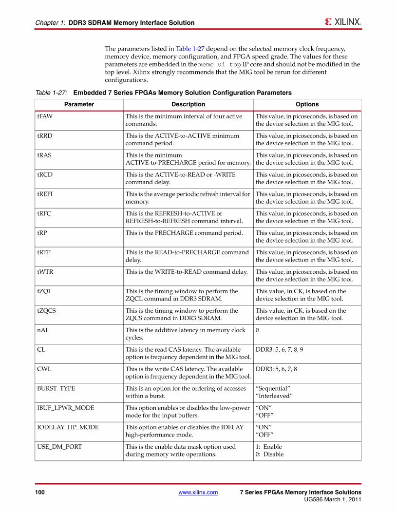
100 www.xilinx.com 7 Series FPGAs Memory Interface SolutionsUG586 March 1, 2011
Chapter 1: DDR3 SDRAM Memory Interface Solution
The parameters listed in Table 1-27 depend on the selected memory clock frequency, memory device, memory configuration, and FPGA speed grade. The values for these parameters are embedded in the memc_ui_top IP core and should not be modified in the top level. Xilinx strongly recommends that the MIG tool be rerun for different configurations.
Table 1-27: Embedded 7 Series FPGAs Memory Solution Configuration Parameters
Parameter Description Options
tFAW This is the minimum interval of four active commands.
This value, in picoseconds, is based on the device selection in the MIG tool.
tRRD This is the ACTIVE-to-ACTIVE minimum command period.
This value, in picoseconds, is based on the device selection in the MIG tool.
tRAS This is the minimum ACTIVE-to-PRECHARGE period for memory.
This value, in picoseconds, is based on the device selection in the MIG tool.
tRCD This is the ACTIVE-to-READ or -WRITE command delay.
This value, in picoseconds, is based on the device selection in the MIG tool.
tREFI This is the average periodic refresh interval for memory.
This value, in picoseconds, is based on the device selection in the MIG tool.
tRFC This is the REFRESH-to-ACTIVE or REFRESH-to-REFRESH command interval.
This value, in picoseconds, is based on the device selection in the MIG tool.
tRP This is the PRECHARGE command period. This value, in picoseconds, is based on the device selection in the MIG tool.
tRTP This is the READ-to-PRECHARGE command delay.
This value, in picoseconds, is based on the device selection in the MIG tool.
tWTR This is the WRITE-to-READ command delay. This value, in picoseconds, is based on the device selection in the MIG tool.
tZQI This is the timing window to perform the ZQCL command in DDR3 SDRAM.
This value, in CK, is based on the device selection in the MIG tool.
tZQCS This is the timing window to perform the ZQCS command in DDR3 SDRAM.
This value, in CK, is based on the device selection in the MIG tool.
nAL This is the additive latency in memory clock cycles.
0
CL This is the read CAS latency. The available option is frequency dependent in the MIG tool.
DDR3: 5, 6, 7, 8, 9
CWL This is the write CAS latency. The available option is frequency dependent in the MIG tool.
DDR3: 5, 6, 7, 8
BURST_TYPE This is an option for the ordering of accesses within a burst.
“Sequential”“Interleaved”
IBUF_LPWR_MODE This option enables or disables the low-power mode for the input buffers.
“ON”“OFF”
IODELAY_HP_MODE This option enables or disables the IDELAY high-performance mode.
“ON””OFF”
USE_DM_PORT This is the enable data mask option used during memory write operations.
1: Enable0: Disable
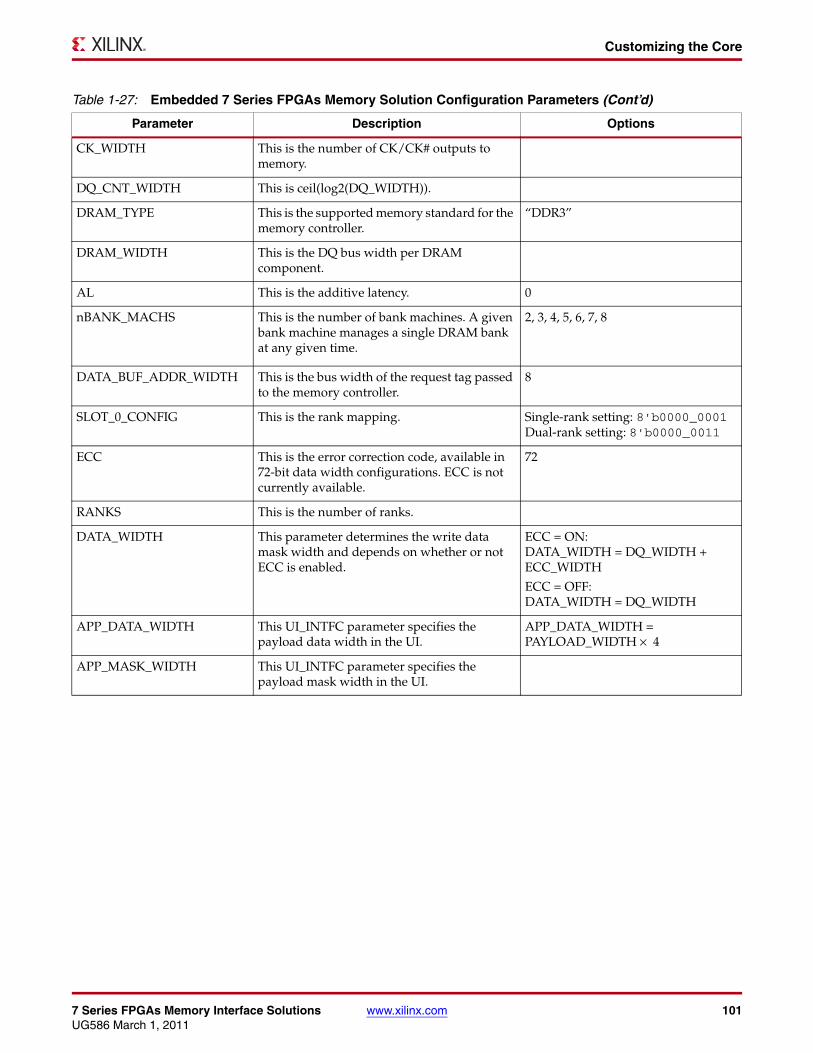
7 Series FPGAs Memory Interface Solutions www.xilinx.com 101UG586 March 1, 2011
Customizing the Core
CK_WIDTH This is the number of CK/CK# outputs to memory.
DQ_CNT_WIDTH This is ceil(log2(DQ_WIDTH)).
DRAM_TYPE This is the supported memory standard for the memory controller.
“DDR3”
DRAM_WIDTH This is the DQ bus width per DRAM component.
AL This is the additive latency. 0
nBANK_MACHS This is the number of bank machines. A given bank machine manages a single DRAM bank at any given time.
2, 3, 4, 5, 6, 7, 8
DATA_BUF_ADDR_WIDTH This is the bus width of the request tag passed to the memory controller.
8
SLOT_0_CONFIG This is the rank mapping. Single-rank setting: 8'b0000_0001Dual-rank setting: 8'b0000_0011
ECC This is the error correction code, available in 72-bit data width configurations. ECC is not currently available.
72
RANKS This is the number of ranks.
DATA_WIDTH This parameter determines the write data mask width and depends on whether or not ECC is enabled.
ECC = ON:DATA_WIDTH = DQ_WIDTH + ECC_WIDTH
ECC = OFF:DATA_WIDTH = DQ_WIDTH
APP_DATA_WIDTH This UI_INTFC parameter specifies the payload data width in the UI.
APP_DATA_WIDTH =PAYLOAD_WIDTH × 4
APP_MASK_WIDTH This UI_INTFC parameter specifies the payload mask width in the UI.
Table 1-27: Embedded 7 Series FPGAs Memory Solution Configuration Parameters (Cont’d)
Parameter Description Options
102 www.xilinx.com 7 Series FPGAs Memory Interface SolutionsUG586 March 1, 2011
Chapter 1: DDR3 SDRAM Memory Interface Solution
Design GuidelinesGuidelines for DDR3 SDRAM designs are covered in this section.
DDR3 SDRAMThis section describes guidelines for DDR3 SDRAM designs, including bank selection, pin allocation, pin assignments, termination, I/O standards, and trace lengths.
Design Rules
Memory types, memory parts, and data widths are restricted based on the selected FPGA, FPGA speed grade, and the design frequency. The final frequency ranges are subject to characterization results.
DDR3 Component PCB Routing
Fly-by routing topology is required for the clock, address, and control lines. Fly-by means that this group of lines is routed in a daisy-chain fashion and terminated appropriately at the end of the line. The trace length of each signal within this group to a given component must be matched. The controller uses write leveling to account for the different skews between components. This technique uses fewer FPGA pins because signals do not have to be replicated.
Pin Assignments
The MIG tool generates pin assignments for a memory interface based on physical layer rules.
Bank and Pin Selection Guides for DDR3 Designs
7 series FPGAs are designed for very high performance memory interfaces, and certain rules must be followed to use the DDR3 SDRAM physical layer. 7 series FPGAs have dedicated logic for each DQS byte group. Four DQS byte groups are available in each 50-pin bank. Each byte group consists of a clock-capable I/O pair for the DQS and ten associated I/Os. In a typical DDR3 configuration, eight of these ten I/Os are used for the DQs, one is used for the data mask (DM), and one is left over for other signals in the memory interface. 7 series FPGAs have dedicated clock routing for high-speed synchronization that is routed vertically within the I/O banks. Thus, DDR3 memory interfaces must be arranged in the banks vertically and not horizontally. In addition, the maximum height is three banks.
The Memory Interface Generator (MIG), when available, should be used to generate a pinout for a 7 series DDR3 interface. The MIG tool follows these rules:
• DQS signals for a byte group must be connected to the clock-capable DQS pair in the bank
• DQ signals must be connected to the byte group pins associated with the corresponding DQS
• Control (RAS_N, CAS_N, WE_N, CS_N) and address lines must be connected to byte groups not used for the data byte groups
• CK must be connected to a clock capable (CCIO) p-n pair in one of the control byte groups
• RESET_N can be connected to any available pin in the interface banks.
7 Series FPGAs Memory Interface Solutions www.xilinx.com 103UG586 March 1, 2011
Design Guidelines
• All CKE and ODT pins of an interface must be in the same bank. They cannot be spread among banks.
• The bank containing the CKE and ODT signals must have either an address/control byte group or an unused byte group
• VRN and VRP are used for the digitally controlled impedance (DCI) reference for banks that support DCI. DCI cascade is permitted; however, only the RESET_N can be placed on the spare VRN/VRP pins.
• The interface must be arranged vertically
• No more than three banks can be used for a single interface
• The system clock input must be in the same column as the memory interface. The system clock input is strongly recommended to be in the address/control bank. If this is not possible (sometimes occurs in single bank 16 bit wide designs), the system clock input must be in the bank above or below the address/control bank.
Bank Sharing Among Controllers
No unused part of a bank used in a memory interface is permitted to be shared with another memory interface. The dedicated logic that controls all the FIFOs and phasers in a bank is designed to only operate with a single memory interface and cannot be shared with other memory interfaces.
Pin Swapping
• Pins can be freely swapped within each byte group (data and address/control), except for the DQS pair which must be on a clock-capable DQS pair, and CK which must be on a clock-capable p-n pair.
• Byte groups (data and address/control) can be freely swapped with each other.
• Pins in the address/control byte groups can be freely swapped within and between their byte groups.
• CKE and ODT can be placed on any unused pin in the memory interface banks except VRN/VRP pins.
• No other pin swapping is permitted.
Note: The MIG tool does not yet support the swapping above. The user needs to update the UCF, the parameters in the RTL, and possibly the RTL itself to implement them.
Table 1-28 shows an example of a 16-bit DDR3 interface contained within one bank. This example is for a component interface using a 2 Gb x16 part. If x8 components are used or a higher density part is needed that would require more address pins, these options are possible:
• An additional bank can be used.
• RESET_N can be moved to another bank as long as timing is met. External timing for this signal is not critical and a level shifter can be used.
• DCI cascade can be used to free up the VRN/VRP pins for the RESET_N if another bank is available for the DCI master.
• ODT can be tied active on the device to free the ODT pin. However, if this option is chosen, only the RTT_WR values are available for termination.
Internal VREF is used in this example.
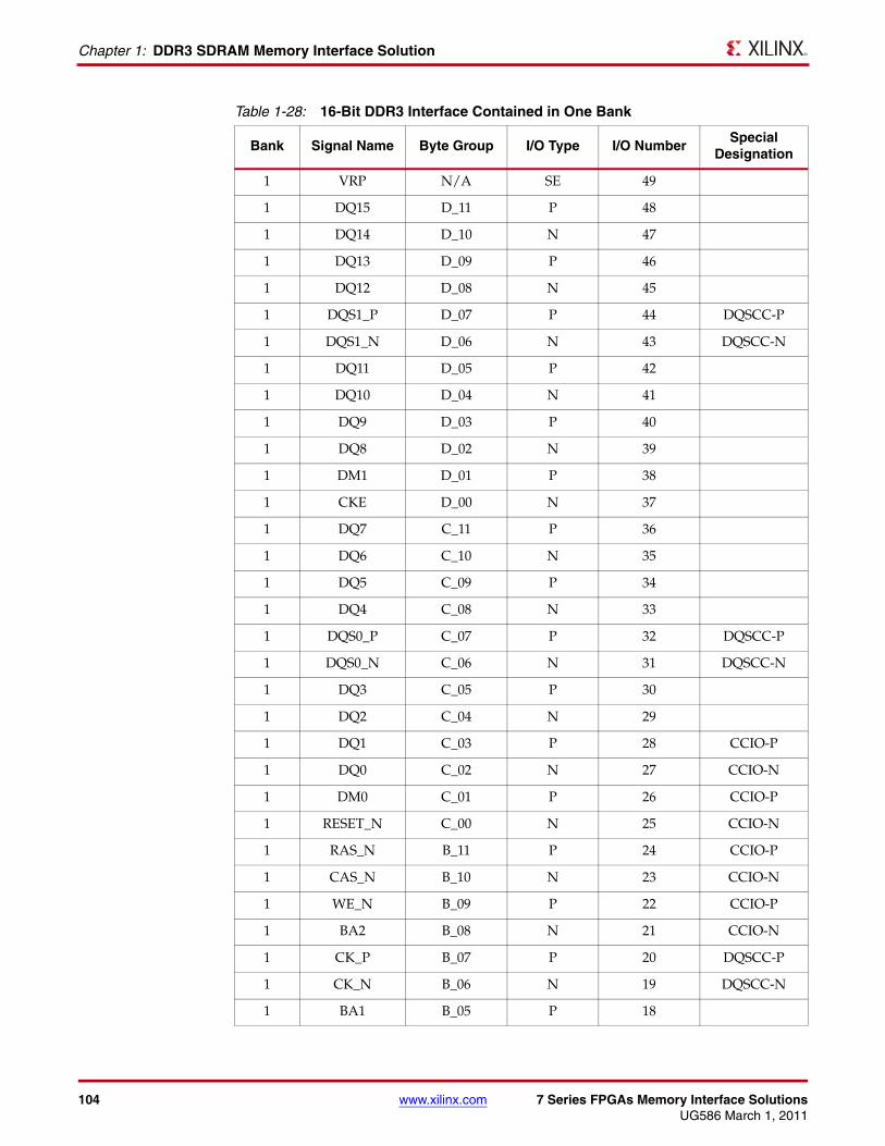
104 www.xilinx.com 7 Series FPGAs Memory Interface SolutionsUG586 March 1, 2011
Chapter 1: DDR3 SDRAM Memory Interface Solution
Table 1-28: 16-Bit DDR3 Interface Contained in One Bank
Bank Signal Name Byte Group I/O Type I/O NumberSpecial
Designation
1 VRP N/A SE 49
1 DQ15 D_11 P 48
1 DQ14 D_10 N 47
1 DQ13 D_09 P 46
1 DQ12 D_08 N 45
1 DQS1_P D_07 P 44 DQSCC-P
1 DQS1_N D_06 N 43 DQSCC-N
1 DQ11 D_05 P 42
1 DQ10 D_04 N 41
1 DQ9 D_03 P 40
1 DQ8 D_02 N 39
1 DM1 D_01 P 38
1 CKE D_00 N 37
1 DQ7 C_11 P 36
1 DQ6 C_10 N 35
1 DQ5 C_09 P 34
1 DQ4 C_08 N 33
1 DQS0_P C_07 P 32 DQSCC-P
1 DQS0_N C_06 N 31 DQSCC-N
1 DQ3 C_05 P 30
1 DQ2 C_04 N 29
1 DQ1 C_03 P 28 CCIO-P
1 DQ0 C_02 N 27 CCIO-N
1 DM0 C_01 P 26 CCIO-P
1 RESET_N C_00 N 25 CCIO-N
1 RAS_N B_11 P 24 CCIO-P
1 CAS_N B_10 N 23 CCIO-N
1 WE_N B_09 P 22 CCIO-P
1 BA2 B_08 N 21 CCIO-N
1 CK_P B_07 P 20 DQSCC-P
1 CK_N B_06 N 19 DQSCC-N
1 BA1 B_05 P 18
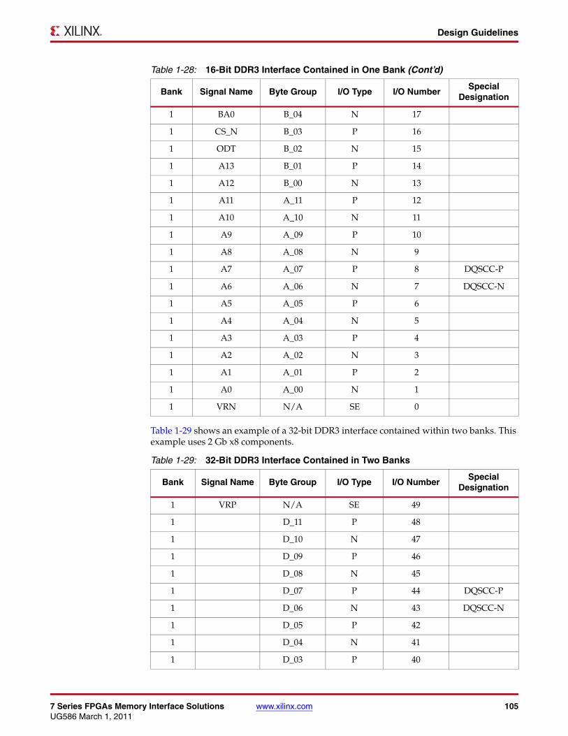
7 Series FPGAs Memory Interface Solutions www.xilinx.com 105UG586 March 1, 2011
Design Guidelines
Table 1-29 shows an example of a 32-bit DDR3 interface contained within two banks. This example uses 2 Gb x8 components.
1 BA0 B_04 N 17
1 CS_N B_03 P 16
1 ODT B_02 N 15
1 A13 B_01 P 14
1 A12 B_00 N 13
1 A11 A_11 P 12
1 A10 A_10 N 11
1 A9 A_09 P 10
1 A8 A_08 N 9
1 A7 A_07 P 8 DQSCC-P
1 A6 A_06 N 7 DQSCC-N
1 A5 A_05 P 6
1 A4 A_04 N 5
1 A3 A_03 P 4
1 A2 A_02 N 3
1 A1 A_01 P 2
1 A0 A_00 N 1
1 VRN N/A SE 0
Table 1-29: 32-Bit DDR3 Interface Contained in Two Banks
Bank Signal Name Byte Group I/O Type I/O NumberSpecial
Designation
1 VRP N/A SE 49
1 D_11 P 48
1 D_10 N 47
1 D_09 P 46
1 D_08 N 45
1 D_07 P 44 DQSCC-P
1 D_06 N 43 DQSCC-N
1 D_05 P 42
1 D_04 N 41
1 D_03 P 40
Table 1-28: 16-Bit DDR3 Interface Contained in One Bank (Cont’d)
Bank Signal Name Byte Group I/O Type I/O NumberSpecial
Designation
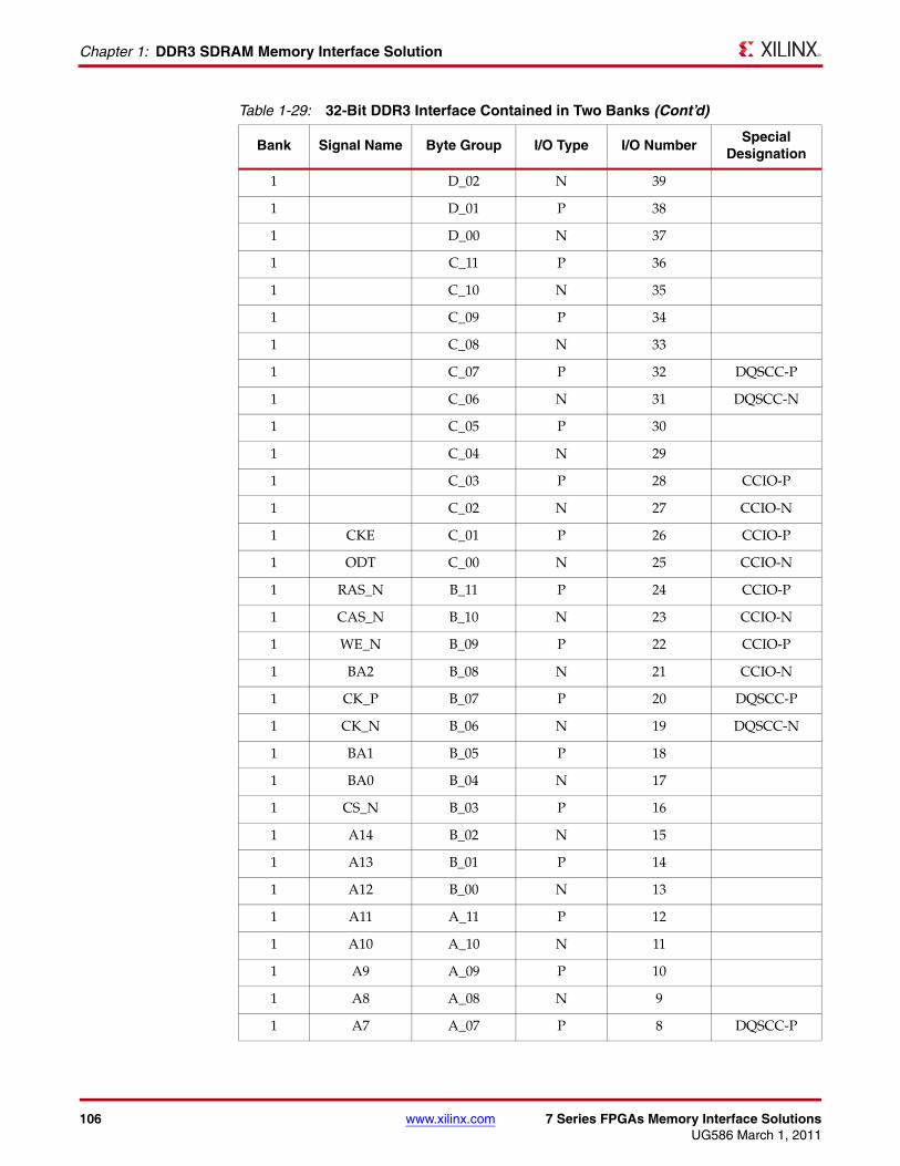
106 www.xilinx.com 7 Series FPGAs Memory Interface SolutionsUG586 March 1, 2011
Chapter 1: DDR3 SDRAM Memory Interface Solution
1 D_02 N 39
1 D_01 P 38
1 D_00 N 37
1 C_11 P 36
1 C_10 N 35
1 C_09 P 34
1 C_08 N 33
1 C_07 P 32 DQSCC-P
1 C_06 N 31 DQSCC-N
1 C_05 P 30
1 C_04 N 29
1 C_03 P 28 CCIO-P
1 C_02 N 27 CCIO-N
1 CKE C_01 P 26 CCIO-P
1 ODT C_00 N 25 CCIO-N
1 RAS_N B_11 P 24 CCIO-P
1 CAS_N B_10 N 23 CCIO-N
1 WE_N B_09 P 22 CCIO-P
1 BA2 B_08 N 21 CCIO-N
1 CK_P B_07 P 20 DQSCC-P
1 CK_N B_06 N 19 DQSCC-N
1 BA1 B_05 P 18
1 BA0 B_04 N 17
1 CS_N B_03 P 16
1 A14 B_02 N 15
1 A13 B_01 P 14
1 A12 B_00 N 13
1 A11 A_11 P 12
1 A10 A_10 N 11
1 A9 A_09 P 10
1 A8 A_08 N 9
1 A7 A_07 P 8 DQSCC-P
Table 1-29: 32-Bit DDR3 Interface Contained in Two Banks (Cont’d)
Bank Signal Name Byte Group I/O Type I/O NumberSpecial
Designation
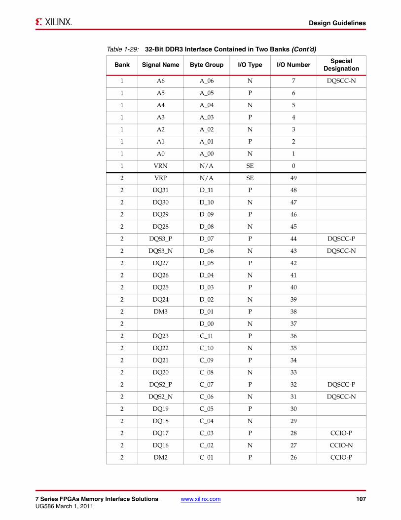
7 Series FPGAs Memory Interface Solutions www.xilinx.com 107UG586 March 1, 2011
Design Guidelines
1 A6 A_06 N 7 DQSCC-N
1 A5 A_05 P 6
1 A4 A_04 N 5
1 A3 A_03 P 4
1 A2 A_02 N 3
1 A1 A_01 P 2
1 A0 A_00 N 1
1 VRN N/A SE 0
2 VRP N/A SE 49
2 DQ31 D_11 P 48
2 DQ30 D_10 N 47
2 DQ29 D_09 P 46
2 DQ28 D_08 N 45
2 DQS3_P D_07 P 44 DQSCC-P
2 DQS3_N D_06 N 43 DQSCC-N
2 DQ27 D_05 P 42
2 DQ26 D_04 N 41
2 DQ25 D_03 P 40
2 DQ24 D_02 N 39
2 DM3 D_01 P 38
2 D_00 N 37
2 DQ23 C_11 P 36
2 DQ22 C_10 N 35
2 DQ21 C_09 P 34
2 DQ20 C_08 N 33
2 DQS2_P C_07 P 32 DQSCC-P
2 DQS2_N C_06 N 31 DQSCC-N
2 DQ19 C_05 P 30
2 DQ18 C_04 N 29
2 DQ17 C_03 P 28 CCIO-P
2 DQ16 C_02 N 27 CCIO-N
2 DM2 C_01 P 26 CCIO-P
Table 1-29: 32-Bit DDR3 Interface Contained in Two Banks (Cont’d)
Bank Signal Name Byte Group I/O Type I/O NumberSpecial
Designation
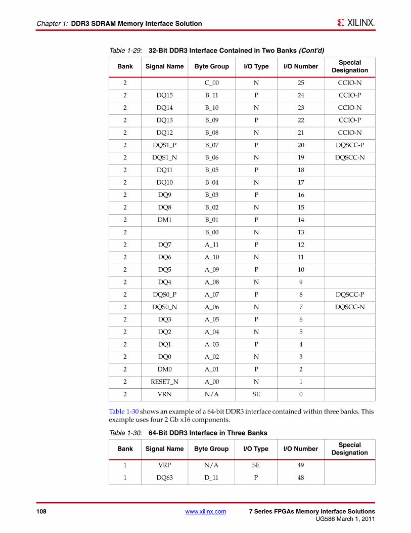
108 www.xilinx.com 7 Series FPGAs Memory Interface SolutionsUG586 March 1, 2011
Chapter 1: DDR3 SDRAM Memory Interface Solution
Table 1-30 shows an example of a 64-bit DDR3 interface contained within three banks. This example uses four 2 Gb x16 components.
2 C_00 N 25 CCIO-N
2 DQ15 B_11 P 24 CCIO-P
2 DQ14 B_10 N 23 CCIO-N
2 DQ13 B_09 P 22 CCIO-P
2 DQ12 B_08 N 21 CCIO-N
2 DQS1_P B_07 P 20 DQSCC-P
2 DQS1_N B_06 N 19 DQSCC-N
2 DQ11 B_05 P 18
2 DQ10 B_04 N 17
2 DQ9 B_03 P 16
2 DQ8 B_02 N 15
2 DM1 B_01 P 14
2 B_00 N 13
2 DQ7 A_11 P 12
2 DQ6 A_10 N 11
2 DQ5 A_09 P 10
2 DQ4 A_08 N 9
2 DQS0_P A_07 P 8 DQSCC-P
2 DQS0_N A_06 N 7 DQSCC-N
2 DQ3 A_05 P 6
2 DQ2 A_04 N 5
2 DQ1 A_03 P 4
2 DQ0 A_02 N 3
2 DM0 A_01 P 2
2 RESET_N A_00 N 1
2 VRN N/A SE 0
Table 1-30: 64-Bit DDR3 Interface in Three Banks
Bank Signal Name Byte Group I/O Type I/O NumberSpecial
Designation
1 VRP N/A SE 49
1 DQ63 D_11 P 48
Table 1-29: 32-Bit DDR3 Interface Contained in Two Banks (Cont’d)
Bank Signal Name Byte Group I/O Type I/O NumberSpecial
Designation

7 Series FPGAs Memory Interface Solutions www.xilinx.com 109UG586 March 1, 2011
Design Guidelines
1 DQ62 D_10 N 47
1 DQ61 D_09 P 46
1 DQ60 D_08 N 45
1 DQS7_P D_07 P 44 DQSCC-P
1 DQS7_N D_06 N 43 DQSCC-N
1 DQ59 D_05 P 42
1 DQ58 D_04 N 41
1 DQ57 D_03 P 40
1 DQ56 D_02 N 39
1 DM7 D_01 P 38
1 D_00 N 37
1 DQ55 C_11 P 36
1 DQ54 C_10 N 35
1 DQ53 C_09 P 34
1 DQ52 C_08 N 33
1 DQS6_P C_07 P 32 DQSCC-P
1 DQS6_N C_06 N 31 DQSCC-N
1 DQ51 C_05 P 30
1 DQ50 C_04 N 29
1 DQ49 C_03 P 28 CCIO-P
1 DQ48 C_02 N 27 CCIO-N
1 DM6 C_01 P 26 CCIO-P
1 C_00 N 25 CCIO-N
1 DQ47 B_11 P 24 CCIO-P
1 DQ46 B_10 N 23 CCIO-N
1 DQ45 B_09 P 22 CCIO-P
1 DQ44 B_08 N 21 CCIO-N
1 DQS5_P B_07 P 20 DQSCC-P
1 DQS5_N B_06 N 19 DQSCC-N
1 DQ43 B_05 P 18
1 DQ42 B_04 N 17
1 DQ41 B_03 P 16
Table 1-30: 64-Bit DDR3 Interface in Three Banks (Cont’d)
Bank Signal Name Byte Group I/O Type I/O NumberSpecial
Designation
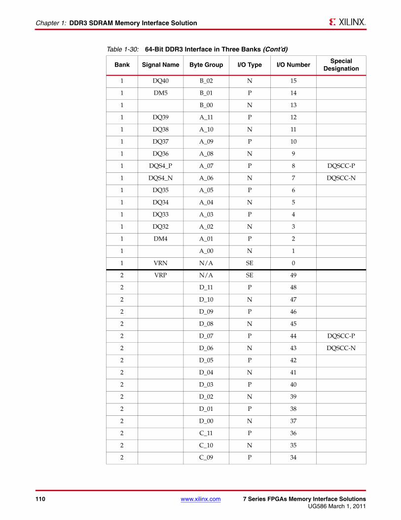
110 www.xilinx.com 7 Series FPGAs Memory Interface SolutionsUG586 March 1, 2011
Chapter 1: DDR3 SDRAM Memory Interface Solution
1 DQ40 B_02 N 15
1 DM5 B_01 P 14
1 B_00 N 13
1 DQ39 A_11 P 12
1 DQ38 A_10 N 11
1 DQ37 A_09 P 10
1 DQ36 A_08 N 9
1 DQS4_P A_07 P 8 DQSCC-P
1 DQS4_N A_06 N 7 DQSCC-N
1 DQ35 A_05 P 6
1 DQ34 A_04 N 5
1 DQ33 A_03 P 4
1 DQ32 A_02 N 3
1 DM4 A_01 P 2
1 A_00 N 1
1 VRN N/A SE 0
2 VRP N/A SE 49
2 D_11 P 48
2 D_10 N 47
2 D_09 P 46
2 D_08 N 45
2 D_07 P 44 DQSCC-P
2 D_06 N 43 DQSCC-N
2 D_05 P 42
2 D_04 N 41
2 D_03 P 40
2 D_02 N 39
2 D_01 P 38
2 D_00 N 37
2 C_11 P 36
2 C_10 N 35
2 C_09 P 34
Table 1-30: 64-Bit DDR3 Interface in Three Banks (Cont’d)
Bank Signal Name Byte Group I/O Type I/O NumberSpecial
Designation
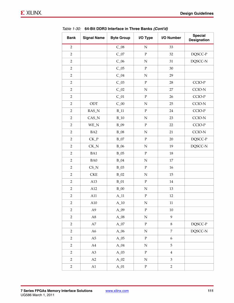
7 Series FPGAs Memory Interface Solutions www.xilinx.com 111UG586 March 1, 2011
Design Guidelines
2 C_08 N 33
2 C_07 P 32 DQSCC-P
2 C_06 N 31 DQSCC-N
2 C_05 P 30
2 C_04 N 29
2 C_03 P 28 CCIO-P
2 C_02 N 27 CCIO-N
2 C_01 P 26 CCIO-P
2 ODT C_00 N 25 CCIO-N
2 RAS_N B_11 P 24 CCIO-P
2 CAS_N B_10 N 23 CCIO-N
2 WE_N B_09 P 22 CCIO-P
2 BA2 B_08 N 21 CCIO-N
2 CK_P B_07 P 20 DQSCC-P
2 CK_N B_06 N 19 DQSCC-N
2 BA1 B_05 P 18
2 BA0 B_04 N 17
2 CS_N B_03 P 16
2 CKE B_02 N 15
2 A13 B_01 P 14
2 A12 B_00 N 13
2 A11 A_11 P 12
2 A10 A_10 N 11
2 A9 A_09 P 10
2 A8 A_08 N 9
2 A7 A_07 P 8 DQSCC-P
2 A6 A_06 N 7 DQSCC-N
2 A5 A_05 P 6
2 A4 A_04 N 5
2 A3 A_03 P 4
2 A2 A_02 N 3
2 A1 A_01 P 2
Table 1-30: 64-Bit DDR3 Interface in Three Banks (Cont’d)
Bank Signal Name Byte Group I/O Type I/O NumberSpecial
Designation
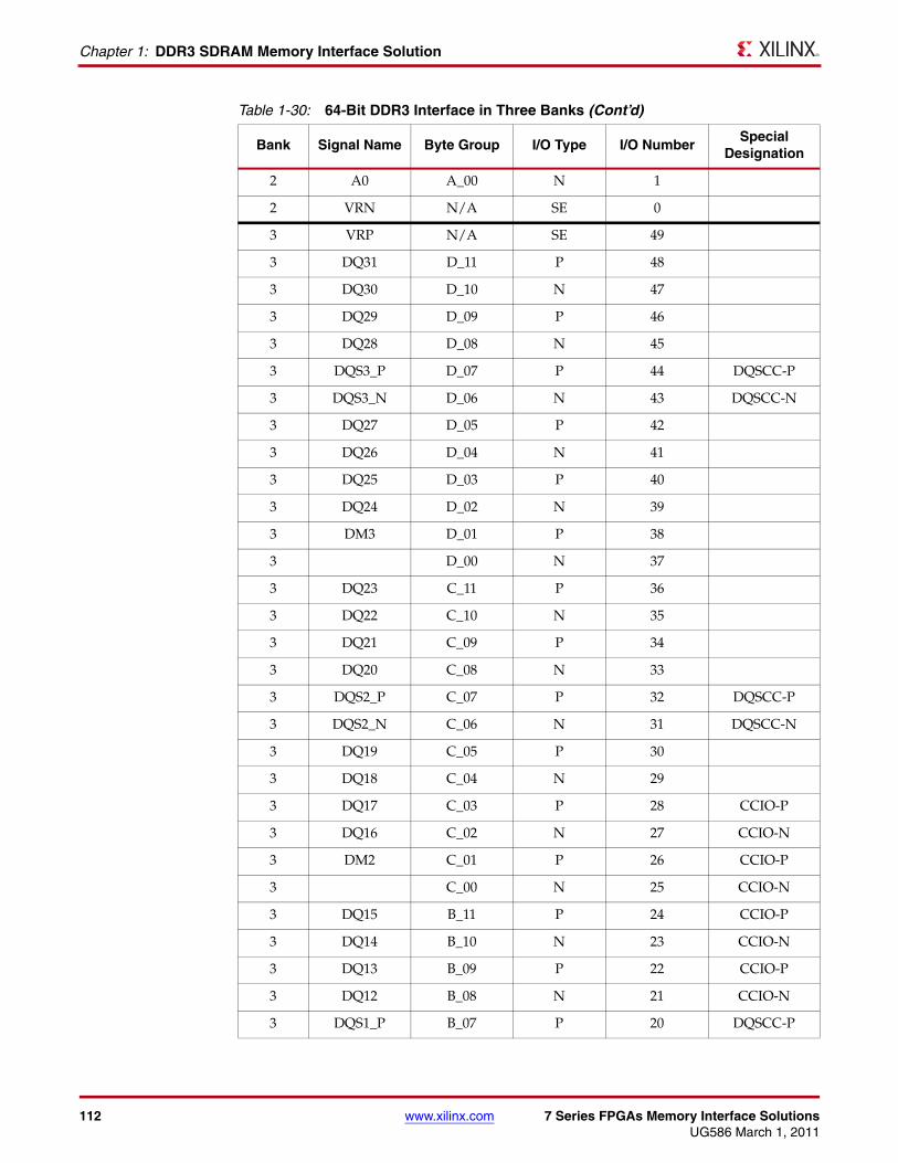
112 www.xilinx.com 7 Series FPGAs Memory Interface SolutionsUG586 March 1, 2011
Chapter 1: DDR3 SDRAM Memory Interface Solution
2 A0 A_00 N 1
2 VRN N/A SE 0
3 VRP N/A SE 49
3 DQ31 D_11 P 48
3 DQ30 D_10 N 47
3 DQ29 D_09 P 46
3 DQ28 D_08 N 45
3 DQS3_P D_07 P 44 DQSCC-P
3 DQS3_N D_06 N 43 DQSCC-N
3 DQ27 D_05 P 42
3 DQ26 D_04 N 41
3 DQ25 D_03 P 40
3 DQ24 D_02 N 39
3 DM3 D_01 P 38
3 D_00 N 37
3 DQ23 C_11 P 36
3 DQ22 C_10 N 35
3 DQ21 C_09 P 34
3 DQ20 C_08 N 33
3 DQS2_P C_07 P 32 DQSCC-P
3 DQS2_N C_06 N 31 DQSCC-N
3 DQ19 C_05 P 30
3 DQ18 C_04 N 29
3 DQ17 C_03 P 28 CCIO-P
3 DQ16 C_02 N 27 CCIO-N
3 DM2 C_01 P 26 CCIO-P
3 C_00 N 25 CCIO-N
3 DQ15 B_11 P 24 CCIO-P
3 DQ14 B_10 N 23 CCIO-N
3 DQ13 B_09 P 22 CCIO-P
3 DQ12 B_08 N 21 CCIO-N
3 DQS1_P B_07 P 20 DQSCC-P
Table 1-30: 64-Bit DDR3 Interface in Three Banks (Cont’d)
Bank Signal Name Byte Group I/O Type I/O NumberSpecial
Designation
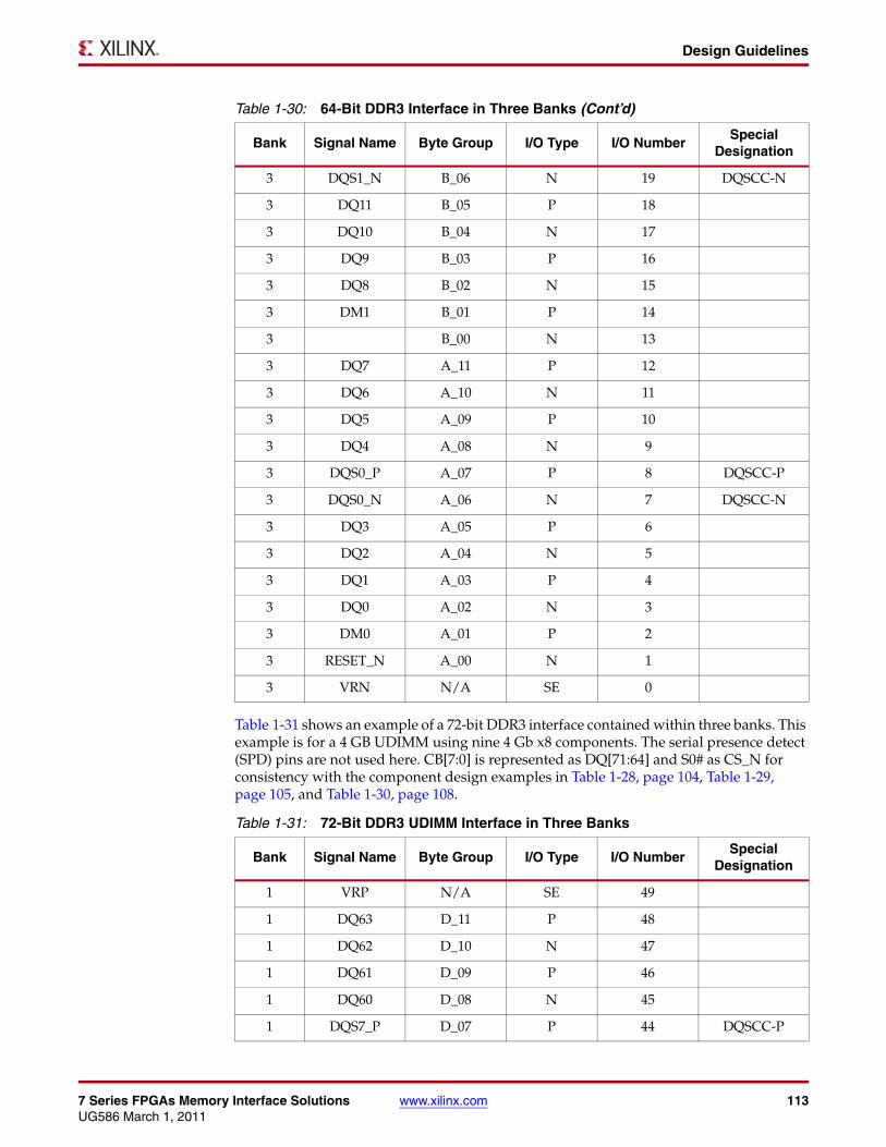
7 Series FPGAs Memory Interface Solutions www.xilinx.com 113UG586 March 1, 2011
Design Guidelines
Table 1-31 shows an example of a 72-bit DDR3 interface contained within three banks. This example is for a 4 GB UDIMM using nine 4 Gb x8 components. The serial presence detect (SPD) pins are not used here. CB[7:0] is represented as DQ[71:64] and S0# as CS_N for consistency with the component design examples in Table 1-28, page 104, Table 1-29, page 105, and Table 1-30, page 108.
3 DQS1_N B_06 N 19 DQSCC-N
3 DQ11 B_05 P 18
3 DQ10 B_04 N 17
3 DQ9 B_03 P 16
3 DQ8 B_02 N 15
3 DM1 B_01 P 14
3 B_00 N 13
3 DQ7 A_11 P 12
3 DQ6 A_10 N 11
3 DQ5 A_09 P 10
3 DQ4 A_08 N 9
3 DQS0_P A_07 P 8 DQSCC-P
3 DQS0_N A_06 N 7 DQSCC-N
3 DQ3 A_05 P 6
3 DQ2 A_04 N 5
3 DQ1 A_03 P 4
3 DQ0 A_02 N 3
3 DM0 A_01 P 2
3 RESET_N A_00 N 1
3 VRN N/A SE 0
Table 1-31: 72-Bit DDR3 UDIMM Interface in Three Banks
Bank Signal Name Byte Group I/O Type I/O NumberSpecial
Designation
1 VRP N/A SE 49
1 DQ63 D_11 P 48
1 DQ62 D_10 N 47
1 DQ61 D_09 P 46
1 DQ60 D_08 N 45
1 DQS7_P D_07 P 44 DQSCC-P
Table 1-30: 64-Bit DDR3 Interface in Three Banks (Cont’d)
Bank Signal Name Byte Group I/O Type I/O NumberSpecial
Designation
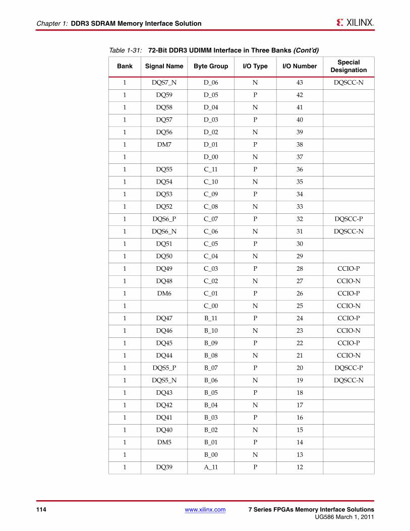
114 www.xilinx.com 7 Series FPGAs Memory Interface SolutionsUG586 March 1, 2011
Chapter 1: DDR3 SDRAM Memory Interface Solution
1 DQS7_N D_06 N 43 DQSCC-N
1 DQ59 D_05 P 42
1 DQ58 D_04 N 41
1 DQ57 D_03 P 40
1 DQ56 D_02 N 39
1 DM7 D_01 P 38
1 D_00 N 37
1 DQ55 C_11 P 36
1 DQ54 C_10 N 35
1 DQ53 C_09 P 34
1 DQ52 C_08 N 33
1 DQS6_P C_07 P 32 DQSCC-P
1 DQS6_N C_06 N 31 DQSCC-N
1 DQ51 C_05 P 30
1 DQ50 C_04 N 29
1 DQ49 C_03 P 28 CCIO-P
1 DQ48 C_02 N 27 CCIO-N
1 DM6 C_01 P 26 CCIO-P
1 C_00 N 25 CCIO-N
1 DQ47 B_11 P 24 CCIO-P
1 DQ46 B_10 N 23 CCIO-N
1 DQ45 B_09 P 22 CCIO-P
1 DQ44 B_08 N 21 CCIO-N
1 DQS5_P B_07 P 20 DQSCC-P
1 DQS5_N B_06 N 19 DQSCC-N
1 DQ43 B_05 P 18
1 DQ42 B_04 N 17
1 DQ41 B_03 P 16
1 DQ40 B_02 N 15
1 DM5 B_01 P 14
1 B_00 N 13
1 DQ39 A_11 P 12
Table 1-31: 72-Bit DDR3 UDIMM Interface in Three Banks (Cont’d)
Bank Signal Name Byte Group I/O Type I/O NumberSpecial
Designation
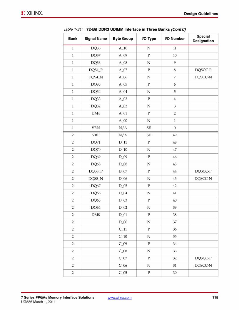
7 Series FPGAs Memory Interface Solutions www.xilinx.com 115UG586 March 1, 2011
Design Guidelines
1 DQ38 A_10 N 11
1 DQ37 A_09 P 10
1 DQ36 A_08 N 9
1 DQS4_P A_07 P 8 DQSCC-P
1 DQS4_N A_06 N 7 DQSCC-N
1 DQ35 A_05 P 6
1 DQ34 A_04 N 5
1 DQ33 A_03 P 4
1 DQ32 A_02 N 3
1 DM4 A_01 P 2
1 A_00 N 1
1 VRN N/A SE 0
2 VRP N/A SE 49
2 DQ71 D_11 P 48
2 DQ70 D_10 N 47
2 DQ69 D_09 P 46
2 DQ68 D_08 N 45
2 DQS8_P D_07 P 44 DQSCC-P
2 DQS8_N D_06 N 43 DQSCC-N
2 DQ67 D_05 P 42
2 DQ66 D_04 N 41
2 DQ65 D_03 P 40
2 DQ64 D_02 N 39
2 DM8 D_01 P 38
2 D_00 N 37
2 C_11 P 36
2 C_10 N 35
2 C_09 P 34
2 C_08 N 33
2 C_07 P 32 DQSCC-P
2 C_06 N 31 DQSCC-N
2 C_05 P 30
Table 1-31: 72-Bit DDR3 UDIMM Interface in Three Banks (Cont’d)
Bank Signal Name Byte Group I/O Type I/O NumberSpecial
Designation
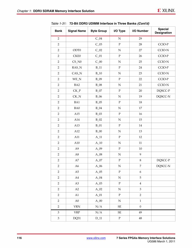
116 www.xilinx.com 7 Series FPGAs Memory Interface SolutionsUG586 March 1, 2011
Chapter 1: DDR3 SDRAM Memory Interface Solution
2 C_04 N 29
2 C_03 P 28 CCIO-P
2 ODT0 C_02 N 27 CCIO-N
2 CKE0 C_01 P 26 CCIO-P
2 CS_N0 C_00 N 25 CCIO-N
2 RAS_N B_11 P 24 CCIO-P
2 CAS_N B_10 N 23 CCIO-N
2 WE_N B_09 P 22 CCIO-P
2 BA2 B_08 N 21 CCIO-N
2 CK_P B_07 P 20 DQSCC-P
2 CK_N B_06 N 19 DQSCC-N
2 BA1 B_05 P 18
2 BA0 B_04 N 17
2 A15 B_03 P 16
2 A14 B_02 N 15
2 A13 B_01 P 14
2 A12 B_00 N 13
2 A11 A_11 P 12
2 A10 A_10 N 11
2 A9 A_09 P 10
2 A8 A_08 N 9
2 A7 A_07 P 8 DQSCC-P
2 A6 A_06 N 7 DQSCC-N
2 A5 A_05 P 6
2 A4 A_04 N 5
2 A3 A_03 P 4
2 A2 A_02 N 3
2 A1 A_01 P 2
2 A0 A_00 N 1
2 VRN N/A SE 0
3 VRP N/A SE 49
3 DQ31 D_11 P 48
Table 1-31: 72-Bit DDR3 UDIMM Interface in Three Banks (Cont’d)
Bank Signal Name Byte Group I/O Type I/O NumberSpecial
Designation

7 Series FPGAs Memory Interface Solutions www.xilinx.com 117UG586 March 1, 2011
Design Guidelines
3 DQ30 D_10 N 47
3 DQ29 D_09 P 46
3 DQ28 D_08 N 45
3 DQS3_P D_07 P 44 DQSCC-P
3 DQS3_N D_06 N 43 DQSCC-N
3 DQ27 D_05 P 42
3 DQ26 D_04 N 41
3 DQ25 D_03 P 40
3 DQ24 D_02 N 39
3 DM3 D_01 P 38
3 D_00 N 37
3 DQ23 C_11 P 36
3 DQ22 C_10 N 35
3 DQ21 C_09 P 34
3 DQ20 C_08 N 33
3 DQS2_P C_07 P 32 DQSCC-P
3 DQS2_N C_06 N 31 DQSCC-N
3 DQ19 C_05 P 30
3 DQ18 C_04 N 29
3 DQ17 C_03 P 28 CCIO-P
3 DQ16 C_02 N 27 CCIO-N
3 DM2 C_01 P 26 CCIO-P
3 C_00 N 25 CCIO-N
3 DQ15 B_11 P 24 CCIO-P
3 DQ14 B_10 N 23 CCIO-N
3 DQ13 B_09 P 22 CCIO-P
3 DQ12 B_08 N 21 CCIO-N
3 DQS1_P B_07 P 20 DQSCC-P
3 DQS1_N B_06 N 19 DQSCC-N
3 DQ11 B_05 P 18
3 DQ10 B_04 N 17
3 DQ9 B_03 P 16
Table 1-31: 72-Bit DDR3 UDIMM Interface in Three Banks (Cont’d)
Bank Signal Name Byte Group I/O Type I/O NumberSpecial
Designation

118 www.xilinx.com 7 Series FPGAs Memory Interface SolutionsUG586 March 1, 2011
Chapter 1: DDR3 SDRAM Memory Interface Solution
Configuration
The UCF contains timing, pin, and I/O standard information. The sys_clk constraint sets the operating frequency of the interface and is set through the MIG GUI. The MIG GUI must be rerun if this needs to be altered, because other internal parameters are affected. For example:
NET "sys_clk_p" TNM_NET = TNM_sys_clk;TIMESPEC "TS_sys_clk" = PERIOD "TNM_sys_clk" 1.875 ns;
The clk_ref constraint sets the frequency for the IDELAY reference clock, which is typically 200 MHz. For example:
NET "clk_ref_p" TNM_NET = TNM_clk_ref;TIMESPEC "TS_clk_ref" = PERIOD "TNM_clk_ref" 5 ns;
The I/O standards are set appropriately for the DDR3 interface with SSTL15, SSTL15_T_DCI, or DIFF_SSTL15_T_DCI, as appropriate. LVDS_25 is used for the system clock (sys_clk) and I/O delay reference clock (clk_ref). These standards can be changed, as required, for the system configuration. These signals are brought out to the top level for system connection:
• sys_rst: This is the main system reset.
• phy_init_done: This signal indicates when the internal calibration is done and that the interface is ready for use.
• error: This signal is generated by the example design’s traffic generator if read data does not match the write data.
3 DQ8 B_02 N 15
3 DM1 B_01 P 14
3 B_00 N 13
3 DQ7 A_11 P 12
3 DQ6 A_10 N 11
3 DQ5 A_09 P 10
3 DQ4 A_08 N 9
3 DQS0_P A_07 P 8 DQSCC-P
3 DQS0_N A_06 N 7 DQSCC-N
3 DQ3 A_05 P 6
3 DQ2 A_04 N 5
3 DQ1 A_03 P 4
3 DQ0 A_02 N 3
3 DM0 A_01 P 2
3 RESET_N A_00 N 1
3 VRN N/A SE 0
Table 1-31: 72-Bit DDR3 UDIMM Interface in Three Banks (Cont’d)
Bank Signal Name Byte Group I/O Type I/O NumberSpecial
Designation
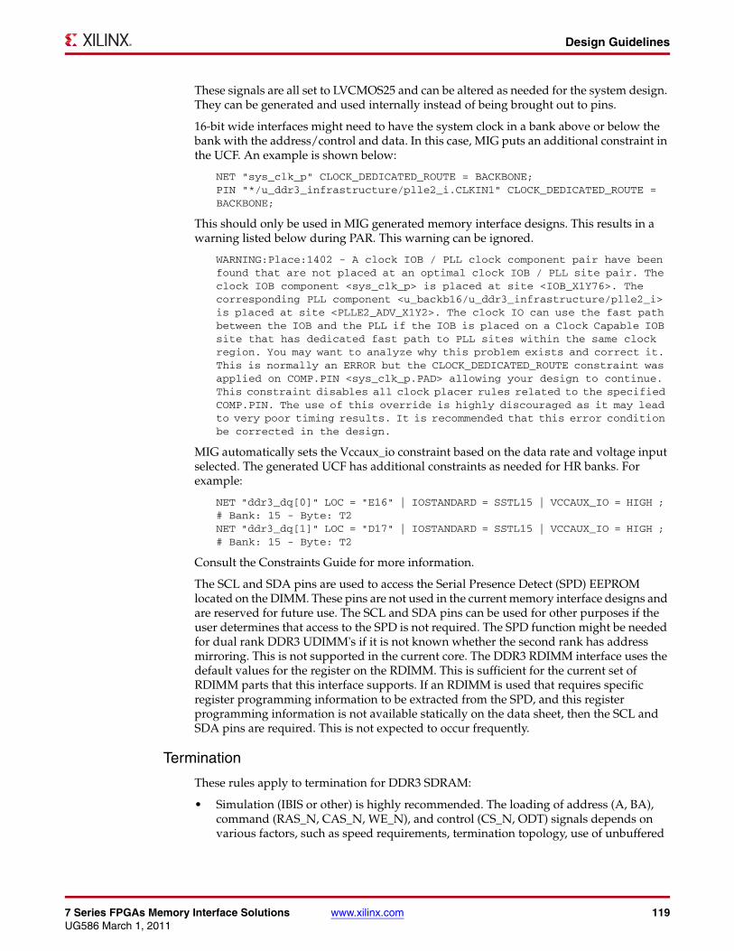
7 Series FPGAs Memory Interface Solutions www.xilinx.com 119UG586 March 1, 2011
Design Guidelines
These signals are all set to LVCMOS25 and can be altered as needed for the system design. They can be generated and used internally instead of being brought out to pins.
16-bit wide interfaces might need to have the system clock in a bank above or below the bank with the address/control and data. In this case, MIG puts an additional constraint in the UCF. An example is shown below:
NET "sys_clk_p" CLOCK_DEDICATED_ROUTE = BACKBONE;PIN "*/u_ddr3_infrastructure/plle2_i.CLKIN1" CLOCK_DEDICATED_ROUTE = BACKBONE;
This should only be used in MIG generated memory interface designs. This results in a warning listed below during PAR. This warning can be ignored.
WARNING:Place:1402 - A clock IOB / PLL clock component pair have been found that are not placed at an optimal clock IOB / PLL site pair. The clock IOB component <sys_clk_p> is placed at site <IOB_X1Y76>. The corresponding PLL component <u_backb16/u_ddr3_infrastructure/plle2_i> is placed at site <PLLE2_ADV_X1Y2>. The clock IO can use the fast path between the IOB and the PLL if the IOB is placed on a Clock Capable IOB site that has dedicated fast path to PLL sites within the same clock region. You may want to analyze why this problem exists and correct it. This is normally an ERROR but the CLOCK_DEDICATED_ROUTE constraint was applied on COMP.PIN <sys_clk_p.PAD> allowing your design to continue. This constraint disables all clock placer rules related to the specified COMP.PIN. The use of this override is highly discouraged as it may lead to very poor timing results. It is recommended that this error condition be corrected in the design.
MIG automatically sets the Vccaux_io constraint based on the data rate and voltage input selected. The generated UCF has additional constraints as needed for HR banks. For example:
NET "ddr3_dq[0]" LOC = "E16" | IOSTANDARD = SSTL15 | VCCAUX_IO = HIGH ; # Bank: 15 - Byte: T2NET "ddr3_dq[1]" LOC = "D17" | IOSTANDARD = SSTL15 | VCCAUX_IO = HIGH ; # Bank: 15 - Byte: T2
Consult the Constraints Guide for more information.
The SCL and SDA pins are used to access the Serial Presence Detect (SPD) EEPROM located on the DIMM. These pins are not used in the current memory interface designs and are reserved for future use. The SCL and SDA pins can be used for other purposes if the user determines that access to the SPD is not required. The SPD function might be needed for dual rank DDR3 UDIMM's if it is not known whether the second rank has address mirroring. This is not supported in the current core. The DDR3 RDIMM interface uses the default values for the register on the RDIMM. This is sufficient for the current set of RDIMM parts that this interface supports. If an RDIMM is used that requires specific register programming information to be extracted from the SPD, and this register programming information is not available statically on the data sheet, then the SCL and SDA pins are required. This is not expected to occur frequently.
Termination
These rules apply to termination for DDR3 SDRAM:
• Simulation (IBIS or other) is highly recommended. The loading of address (A, BA), command (RAS_N, CAS_N, WE_N), and control (CS_N, ODT) signals depends on various factors, such as speed requirements, termination topology, use of unbuffered
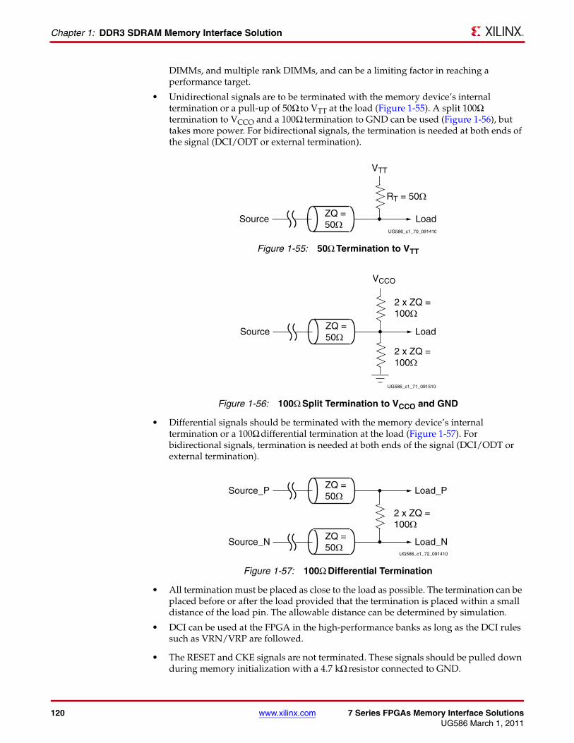
120 www.xilinx.com 7 Series FPGAs Memory Interface SolutionsUG586 March 1, 2011
Chapter 1: DDR3 SDRAM Memory Interface Solution
DIMMs, and multiple rank DIMMs, and can be a limiting factor in reaching a performance target.
• Unidirectional signals are to be terminated with the memory device’s internal termination or a pull-up of 50Ω to VTT at the load (Figure 1-55). A split 100Ω termination to VCCO and a 100Ω termination to GND can be used (Figure 1-56), but takes more power. For bidirectional signals, the termination is needed at both ends of the signal (DCI/ODT or external termination).
• Differential signals should be terminated with the memory device’s internal termination or a 100Ω differential termination at the load (Figure 1-57). For bidirectional signals, termination is needed at both ends of the signal (DCI/ODT or external termination).
• All termination must be placed as close to the load as possible. The termination can be placed before or after the load provided that the termination is placed within a small distance of the load pin. The allowable distance can be determined by simulation.
• DCI can be used at the FPGA in the high-performance banks as long as the DCI rules such as VRN/VRP are followed.
• The RESET and CKE signals are not terminated. These signals should be pulled down during memory initialization with a 4.7 kΩ resistor connected to GND.
X-Ref Target - Figure 1-55
Figure 1-55: 50Ω Termination to VTT
X-Ref Target - Figure 1-56
Figure 1-56: 100Ω Split Termination to VCCO and GND
X-Ref Target - Figure 1-57
Figure 1-57: 100Ω Differential Termination
UG586_c1_70_091410
ZQ =50Ω
RT = 50Ω
VTT
LoadSource
UG586_c1_71_091510
ZQ =50Ω
2 x ZQ =100Ω
2 x ZQ =100Ω
VCCO
LoadSource
UG586_c1_72_091410
ZQ =50Ω
2 x ZQ =100Ω
Load_PSource_P
ZQ =50Ω Load_NSource_N
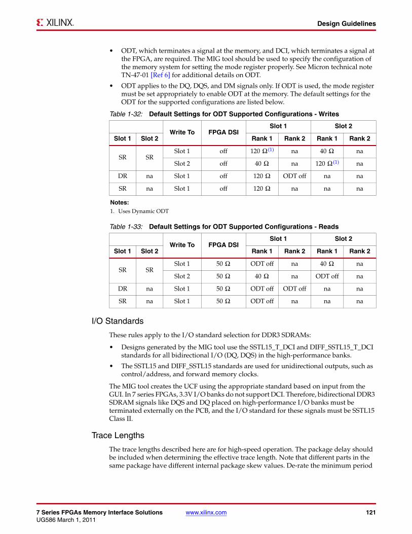
7 Series FPGAs Memory Interface Solutions www.xilinx.com 121UG586 March 1, 2011
Design Guidelines
• ODT, which terminates a signal at the memory, and DCI, which terminates a signal at the FPGA, are required. The MIG tool should be used to specify the configuration of the memory system for setting the mode register properly. See Micron technical note TN-47-01 [Ref 6] for additional details on ODT.
• ODT applies to the DQ, DQS, and DM signals only. If ODT is used, the mode register must be set appropriately to enable ODT at the memory. The default settings for the ODT for the supported configurations are listed below.
I/O Standards
These rules apply to the I/O standard selection for DDR3 SDRAMs:
• Designs generated by the MIG tool use the SSTL15_T_DCI and DIFF_SSTL15_T_DCI standards for all bidirectional I/O (DQ, DQS) in the high-performance banks.
• The SSTL15 and DIFF_SSTL15 standards are used for unidirectional outputs, such as control/address, and forward memory clocks.
The MIG tool creates the UCF using the appropriate standard based on input from the GUI. In 7 series FPGAs, 3.3V I/O banks do not support DCI. Therefore, bidirectional DDR3 SDRAM signals like DQS and DQ placed on high-performance I/O banks must be terminated externally on the PCB, and the I/O standard for these signals must be SSTL15 Class II.
Trace Lengths
The trace lengths described here are for high-speed operation. The package delay should be included when determining the effective trace length. Note that different parts in the same package have different internal package skew values. De-rate the minimum period
Table 1-32: Default Settings for ODT Supported Configurations - Writes
Write To FPGA DSISlot 1 Slot 2
Slot 1 Slot 2 Rank 1 Rank 2 Rank 1 Rank 2
SR SRSlot 1 off 120 (1) na 40 na
Slot 2 off 40 na 120 (1) na
DR na Slot 1 off 120 ODT off na na
SR na Slot 1 off 120 na na na
Notes: 1. Uses Dynamic ODT
Table 1-33: Default Settings for ODT Supported Configurations - Reads
Write To FPGA DSISlot 1 Slot 2
Slot 1 Slot 2 Rank 1 Rank 2 Rank 1 Rank 2
SR SRSlot 1 50 ODT off na 40 na
Slot 2 50 40 na ODT off na
DR na Slot 1 50 ODT off ODT off na na
SR na Slot 1 50 ODT off na na na
Ω Ω
Ω Ω
Ω
Ω
Ω Ω
Ω Ω
Ω
Ω
122 www.xilinx.com 7 Series FPGAs Memory Interface SolutionsUG586 March 1, 2011
Chapter 1: DDR3 SDRAM Memory Interface Solution
appropriately in the MIG Controller Options page when different parts in the same package are used.
The most accurate and recommended method for determining the delay is to use the L and C values for each pin from the IBIS models. The delay value is determined as the square root of (L × C).
Alternatively, a less accurate method is to use PARTGen. The PARTGen utility generates a PKG file that contains the package trace length in microns (µm) for every pin of the device under consideration. For example, to obtain the package delay information for the 7 series FPGA XC7K160T-FF676, this command should be issued:
partgen -v xc7k160tff676
This generates a file named xc7k160tff676.pkg in the current directory with package trace length information for each pin in microns. A typical 6.5 fs/micron (6.5 ps/mm) conversion formula should be used to obtain the corresponding electrical propagation delay. While applying specific trace-matching guidelines for the DDR3 SDRAM interface, this additional package delay term should be considered for the overall electrical propagation delay. Different die in the same package might have different delays for the same package pin. If this is expected, the values should be averaged appropriately. This decreases the maximum possible performance for the target device. These rules indicate the maximum electrical delays between DDR3 SDRAM signals:
• The maximum electrical delay between any DQ and its associated DQS/DQS# should be ±5 ps.
• The maximum electrical delay between any address and control signals and the corresponding CK/CK# should be ±25 ps.
• The maximum electrical delay of any DQS/DQS# should be less than that of CK/CK#.
DQ to DQS matching can be relaxed by the change in clock period as the frequency is lowered from the maximum. For example, if the maximum supported frequency for a configuration is 533 MHz, then the bit time at this frequency is 937.5 ps. The DQ to DQS PCB skew is allowed to be +/- 5ps. If this design is operated at 400 MHz, the bit time is 1250 ps. The change in period is 1250 minus 937.5 or 312.5 ps. Half of this is 156 ps. Thus the new skew allowed is +/- (156+5) or +/- 161 ps.
Write leveling is required for both DIMMs and components. Designs using multiple components should arrange the components in a fly-by routing topology similar to a DIMM where the address, control, and clocks are shared between the components and the signal arrives at each component at a different time. The data bus routing for each component should be as short as possible. Each signal should be routed on a single PCB layer to minimize discontinuities caused by additional vias.
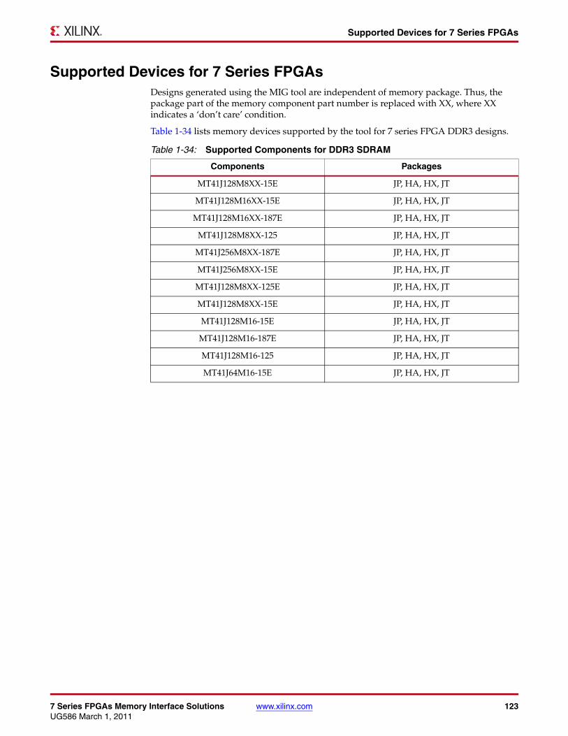
7 Series FPGAs Memory Interface Solutions www.xilinx.com 123UG586 March 1, 2011
Supported Devices for 7 Series FPGAs
Supported Devices for 7 Series FPGAsDesigns generated using the MIG tool are independent of memory package. Thus, the package part of the memory component part number is replaced with XX, where XX indicates a ‘don’t care’ condition.
Table 1-34 lists memory devices supported by the tool for 7 series FPGA DDR3 designs.
Table 1-34: Supported Components for DDR3 SDRAM
Components Packages
MT41J128M8XX-15E JP, HA, HX, JT
MT41J128M16XX-15E JP, HA, HX, JT
MT41J128M16XX-187E JP, HA, HX, JT
MT41J128M8XX-125 JP, HA, HX, JT
MT41J256M8XX-187E JP, HA, HX, JT
MT41J256M8XX-15E JP, HA, HX, JT
MT41J128M8XX-125E JP, HA, HX, JT
MT41J128M8XX-15E JP, HA, HX, JT
MT41J128M16-15E JP, HA, HX, JT
MT41J128M16-187E JP, HA, HX, JT
MT41J128M16-125 JP, HA, HX, JT
MT41J64M16-15E JP, HA, HX, JT
124 www.xilinx.com 7 Series FPGAs Memory Interface SolutionsUG586 March 1, 2011
Chapter 1: DDR3 SDRAM Memory Interface Solution
7 Series FPGAs Memory Interface Solutions www.xilinx.com 125UG586 March 1, 2011
Chapter 2
QDRII+ Memory Interface Solution
IntroductionThe QDRII+ SRAM memory interface solution is a physical layer for interfacing 7 series FPGA user designs to QDRII+ SRAM devices. QDRII+ SRAMs are the latest generation of QDR SRAM devices that offer high-speed data transfers on separate read and write buses on the rising and falling edges of the clock. These memory devices are used in high-performance systems as temporary data storage, such as:
• Look-up tables in networking systems
• Packet buffers in network switches
• Cache memory in high-speed computing
• Data buffers in high-performance testers
The QDRII+ SRAM memory solutions core is a PHY that takes simple user commands, converts them to the QDRII+ protocol, and provides the converted commands to the memory. The PHY’s half-frequency design enables the user to provide one read and one write request per cycle eliminating the need for a memory controller and the associated overhead, thereby reducing the latency through the core. Unique capabilities of the 7 series family allow the PHY to maximize performance and simplify read data capture within the FPGA. The full solution is complete with a synthesizable reference design.
This chapter describes the core architecture and information about using, customizing, and simulating a LogiCORE™ IP QDRII+ SRAM memory interface core for the 7 series FPGAs. Although this soft memory controller core is a fully verified solution with guaranteed performance, termination and trace routing rules for PCB design need to be followed to have the best possible design. For detailed board design guidelines, see Design Guidelines, page 161.
For detailed information and updates about the 7 series FPGA QDRII+ SRAM memory interface core, see the 7 series FPGA data sheets [Ref 10], [Ref 14] on the 7 series FPGA memory interface product page.
Getting Started with the CORE Generator SoftwareThis section is a step-by-step guide for using the CORE Generator™ software to generate a QDRII+ SRAM memory interface in a 7 series FPGA, run the design through implementation with the Xilinx tools, and simulate the example design using the synthesizable test bench provided.
System Requirements• ISE® Design Suite, version 13.1
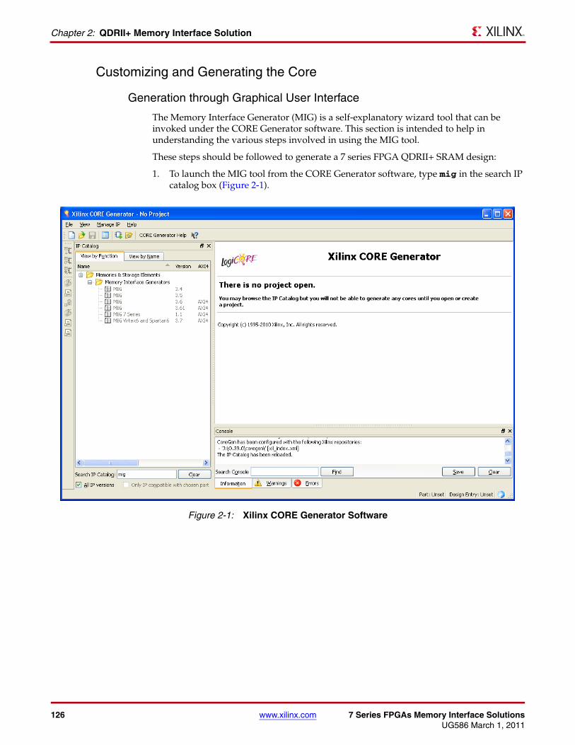
126 www.xilinx.com 7 Series FPGAs Memory Interface SolutionsUG586 March 1, 2011
Chapter 2: QDRII+ Memory Interface Solution
Customizing and Generating the Core
Generation through Graphical User Interface
The Memory Interface Generator (MIG) is a self-explanatory wizard tool that can be invoked under the CORE Generator software. This section is intended to help in understanding the various steps involved in using the MIG tool.
These steps should be followed to generate a 7 series FPGA QDRII+ SRAM design:
1. To launch the MIG tool from the CORE Generator software, type mig in the search IP catalog box (Figure 2-1).
X-Ref Target - Figure 2-1
Figure 2-1: Xilinx CORE Generator Software

7 Series FPGAs Memory Interface Solutions www.xilinx.com 127UG586 March 1, 2011
Getting Started with the CORE Generator Software
2. Choose File → New Project to open the New Project dialog box. Create a new project named 7Series_MIG_Example_Design (Figure 2-2).
3. Enter a project name and location. Click Save (Figure 2-3).
4. Select these project options for the part (Figure 2-4):
• Select the target Kintex-7 or Virtex-7 part.
X-Ref Target - Figure 2-2
Figure 2-2: New CORE Generator Software Project
X-Ref Target - Figure 2-3
Figure 2-3: New Project Menu
UG586_c1_02_091410
UG586_c1_03_111010

128 www.xilinx.com 7 Series FPGAs Memory Interface SolutionsUG586 March 1, 2011
Chapter 2: QDRII+ Memory Interface Solution
X-Ref Target - Figure 2-4
Figure 2-4: CORE Generator Software Device Selection Page
UG586_c1_04_110610

7 Series FPGAs Memory Interface Solutions www.xilinx.com 129UG586 March 1, 2011
Getting Started with the CORE Generator Software
5. Select Verilog as the Design Entry Option and ISE for the Vendor Flow Setting. Click OK to finish the Project Options setup (Figure 2-5).
X-Ref Target - Figure 2-5
Figure 2-5: CORE Generator Software Design Flow Setting Page
UG586_c1_05_110610
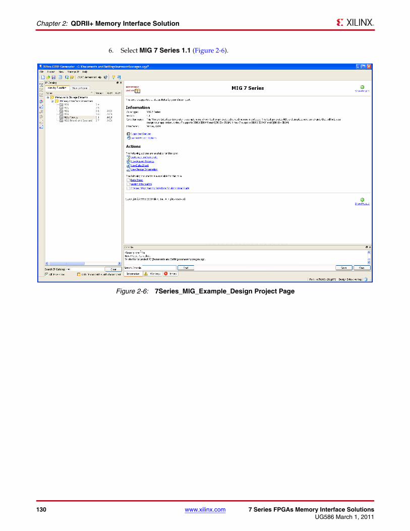
130 www.xilinx.com 7 Series FPGAs Memory Interface SolutionsUG586 March 1, 2011
Chapter 2: QDRII+ Memory Interface Solution
6. Select MIG 7 Series 1.1 (Figure 2-6).X-Ref Target - Figure 2-6
Figure 2-6: 7Series_MIG_Example_Design Project Page
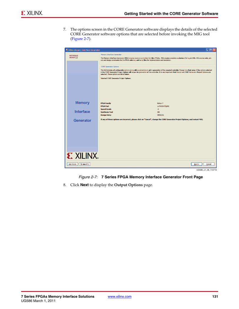
7 Series FPGAs Memory Interface Solutions www.xilinx.com 131UG586 March 1, 2011
Getting Started with the CORE Generator Software
7. The options screen in the CORE Generator software displays the details of the selected CORE Generator software options that are selected before invoking the MIG tool (Figure 2-7).
8. Click Next to display the Output Options page.
X-Ref Target - Figure 2-7
Figure 2-7: 7 Series FPGA Memory Interface Generator Front Page
UG586_c1_08_110710
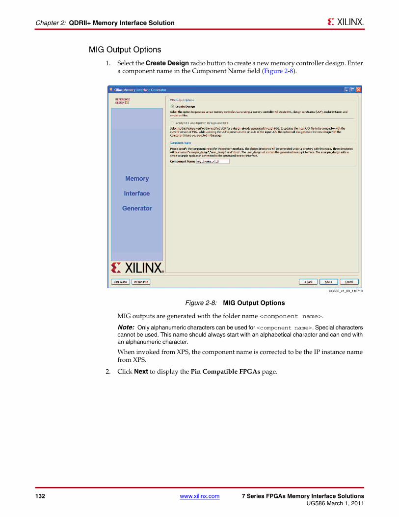
132 www.xilinx.com 7 Series FPGAs Memory Interface SolutionsUG586 March 1, 2011
Chapter 2: QDRII+ Memory Interface Solution
MIG Output Options
1. Select the Create Design radio button to create a new memory controller design. Enter a component name in the Component Name field (Figure 2-8).
MIG outputs are generated with the folder name <component name>.
Note: Only alphanumeric characters can be used for <component name>. Special characters cannot be used. This name should always start with an alphabetical character and can end with an alphanumeric character.
When invoked from XPS, the component name is corrected to be the IP instance name from XPS.
2. Click Next to display the Pin Compatible FPGAs page.
X-Ref Target - Figure 2-8
Figure 2-8: MIG Output Options
UG586_c1_09_110710

7 Series FPGAs Memory Interface Solutions www.xilinx.com 133UG586 March 1, 2011
Getting Started with the CORE Generator Software
Pin Compatible FPGAs
The Pin Compatible FPGAs page lists FPGAs in the selected family having the same package. If the generated pinout from the MIG tool needs to be compatible with any of these other FPGAs, this option should be used to select the FPGAs with which the pinout has to be compatible (Figure 2-9).
1. Select any of the compatible FPGAs in the list. Only the common pins between the target and selected FPGAs are used by the MIG tool. The name in the text box signifies the target FPGA selected.
2. Click Next to display the Memory Selection page.
X-Ref Target - Figure 2-9
Figure 2-9: Pin-Compatible 7 Series FPGAs
UG586_c1_10_110610
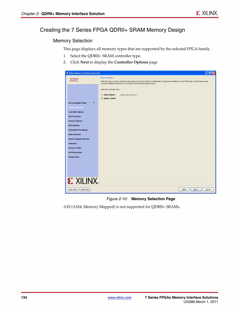
134 www.xilinx.com 7 Series FPGAs Memory Interface SolutionsUG586 March 1, 2011
Chapter 2: QDRII+ Memory Interface Solution
Creating the 7 Series FPGA QDRII+ SRAM Memory Design
Memory Selection
This page displays all memory types that are supported by the selected FPGA family.
1. Select the QDRII+ SRAM controller type.
2. Click Next to display the Controller Options page
AXI (AXI4, Memory Mapped) is not supported for QDRII+ SRAMs.
X-Ref Target - Figure 2-10
Figure 2-10: Memory Selection Page
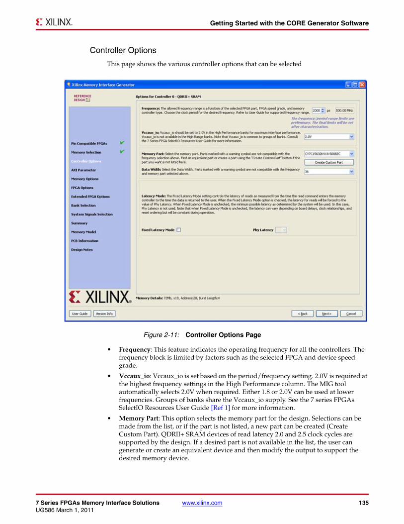
7 Series FPGAs Memory Interface Solutions www.xilinx.com 135UG586 March 1, 2011
Getting Started with the CORE Generator Software
Controller Options
This page shows the various controller options that can be selected
• Frequency: This feature indicates the operating frequency for all the controllers. The frequency block is limited by factors such as the selected FPGA and device speed grade.
• Vccaux_io: Vccaux_io is set based on the period/frequency setting. 2.0V is required at the highest frequency settings in the High Performance column. The MIG tool automatically selects 2.0V when required. Either 1.8 or 2.0V can be used at lower frequencies. Groups of banks share the Vccaux_io supply. See the 7 series FPGAs SelectIO Resources User Guide [Ref 1] for more information.
• Memory Part: This option selects the memory part for the design. Selections can be made from the list, or if the part is not listed, a new part can be created (Create Custom Part). QDRII+ SRAM devices of read latency 2.0 and 2.5 clock cycles are supported by the design. If a desired part is not available in the list, the user can generate or create an equivalent device and then modify the output to support the desired memory device.
X-Ref Target - Figure 2-11
Figure 2-11: Controller Options Page
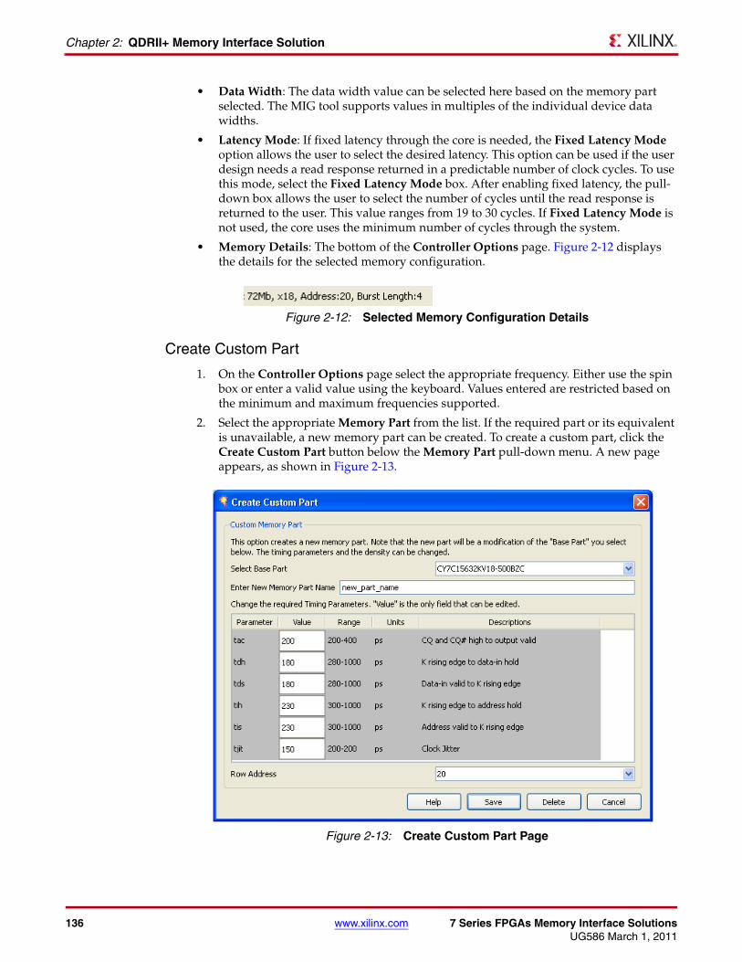
136 www.xilinx.com 7 Series FPGAs Memory Interface SolutionsUG586 March 1, 2011
Chapter 2: QDRII+ Memory Interface Solution
• Data Width: The data width value can be selected here based on the memory part selected. The MIG tool supports values in multiples of the individual device data widths.
• Latency Mode: If fixed latency through the core is needed, the Fixed Latency Mode option allows the user to select the desired latency. This option can be used if the user design needs a read response returned in a predictable number of clock cycles. To use this mode, select the Fixed Latency Mode box. After enabling fixed latency, the pull-down box allows the user to select the number of cycles until the read response is returned to the user. This value ranges from 19 to 30 cycles. If Fixed Latency Mode is not used, the core uses the minimum number of cycles through the system.
• Memory Details: The bottom of the Controller Options page. Figure 2-12 displays the details for the selected memory configuration.
Create Custom Part
1. On the Controller Options page select the appropriate frequency. Either use the spin box or enter a valid value using the keyboard. Values entered are restricted based on the minimum and maximum frequencies supported.
2. Select the appropriate Memory Part from the list. If the required part or its equivalent is unavailable, a new memory part can be created. To create a custom part, click the Create Custom Part button below the Memory Part pull-down menu. A new page appears, as shown in Figure 2-13.
X-Ref Target - Figure 2-12
Figure 2-12: Selected Memory Configuration Details
X-Ref Target - Figure 2-13
Figure 2-13: Create Custom Part Page
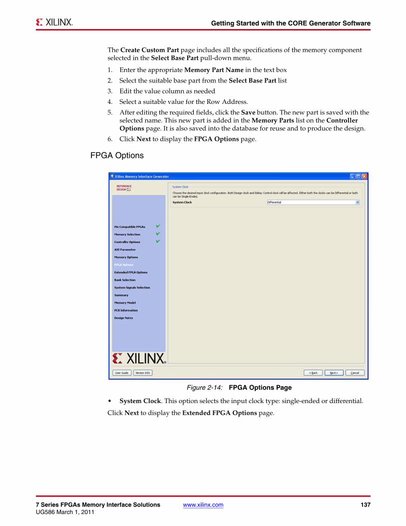
7 Series FPGAs Memory Interface Solutions www.xilinx.com 137UG586 March 1, 2011
Getting Started with the CORE Generator Software
The Create Custom Part page includes all the specifications of the memory component selected in the Select Base Part pull-down menu.
1. Enter the appropriate Memory Part Name in the text box
2. Select the suitable base part from the Select Base Part list
3. Edit the value column as needed
4. Select a suitable value for the Row Address.
5. After editing the required fields, click the Save button. The new part is saved with the selected name. This new part is added in the Memory Parts list on the Controller Options page. It is also saved into the database for reuse and to produce the design.
6. Click Next to display the FPGA Options page.
FPGA Options
• System Clock. This option selects the input clock type: single-ended or differential.
Click Next to display the Extended FPGA Options page.
X-Ref Target - Figure 2-14
Figure 2-14: FPGA Options Page
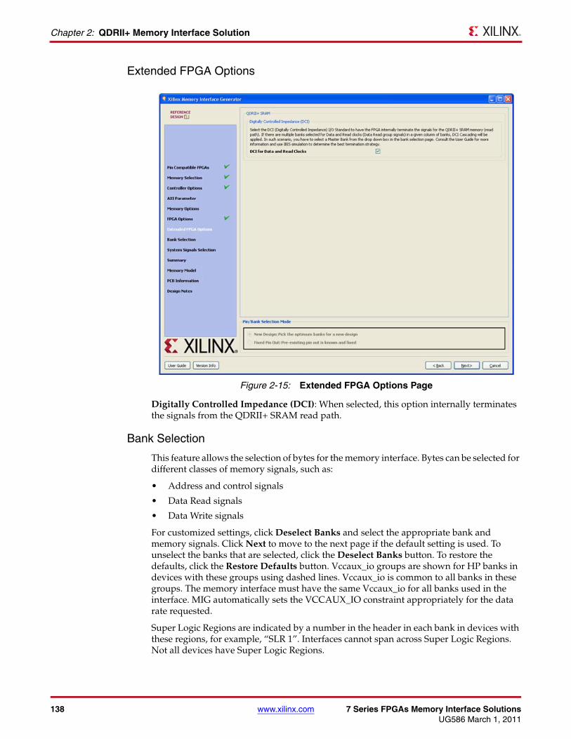
138 www.xilinx.com 7 Series FPGAs Memory Interface SolutionsUG586 March 1, 2011
Chapter 2: QDRII+ Memory Interface Solution
Extended FPGA Options
Digitally Controlled Impedance (DCI): When selected, this option internally terminates the signals from the QDRII+ SRAM read path.
Bank Selection
This feature allows the selection of bytes for the memory interface. Bytes can be selected for different classes of memory signals, such as:
• Address and control signals
• Data Read signals
• Data Write signals
For customized settings, click Deselect Banks and select the appropriate bank and memory signals. Click Next to move to the next page if the default setting is used. To unselect the banks that are selected, click the Deselect Banks button. To restore the defaults, click the Restore Defaults button. Vccaux_io groups are shown for HP banks in devices with these groups using dashed lines. Vccaux_io is common to all banks in these groups. The memory interface must have the same Vccaux_io for all banks used in the interface. MIG automatically sets the VCCAUX_IO constraint appropriately for the data rate requested.
Super Logic Regions are indicated by a number in the header in each bank in devices with these regions, for example, “SLR 1”. Interfaces cannot span across Super Logic Regions. Not all devices have Super Logic Regions.
X-Ref Target - Figure 2-15
Figure 2-15: Extended FPGA Options Page
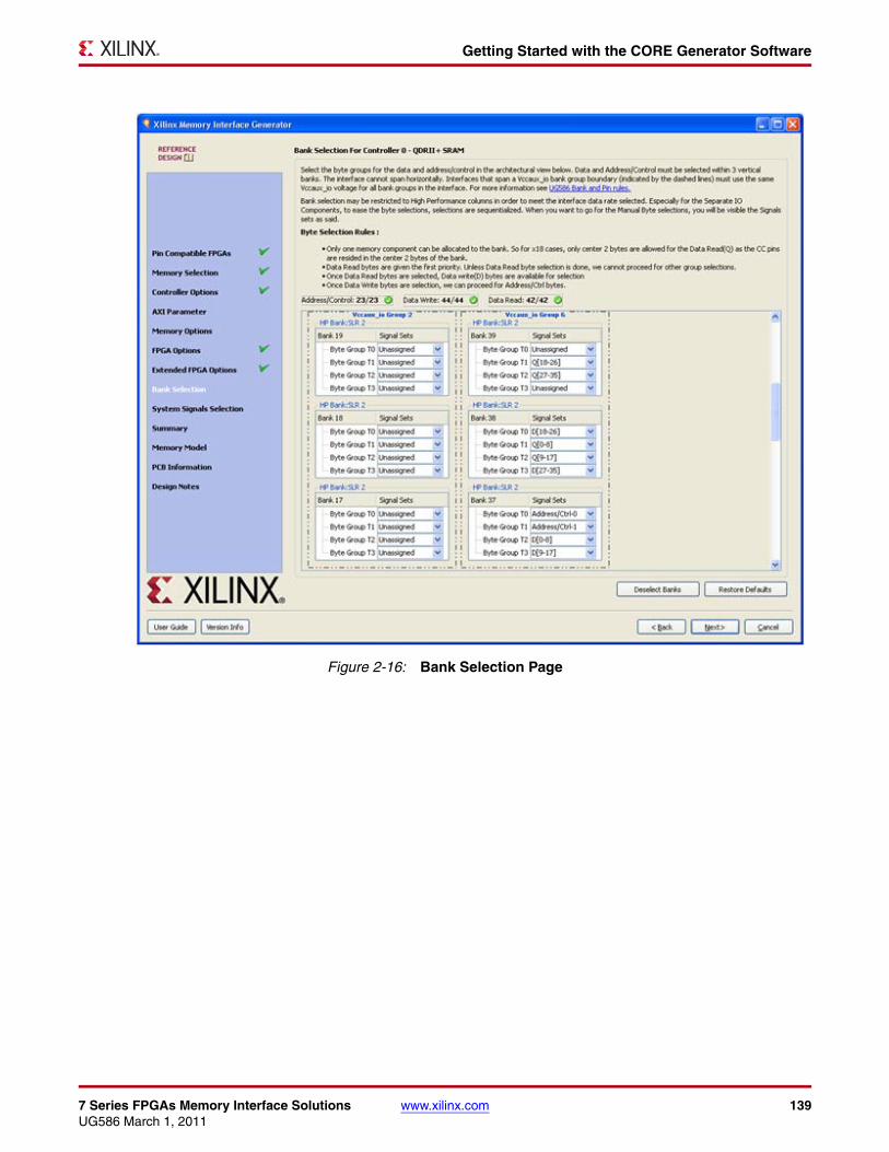
7 Series FPGAs Memory Interface Solutions www.xilinx.com 139UG586 March 1, 2011
Getting Started with the CORE Generator Software
X-Ref Target - Figure 2-16
Figure 2-16: Bank Selection Page
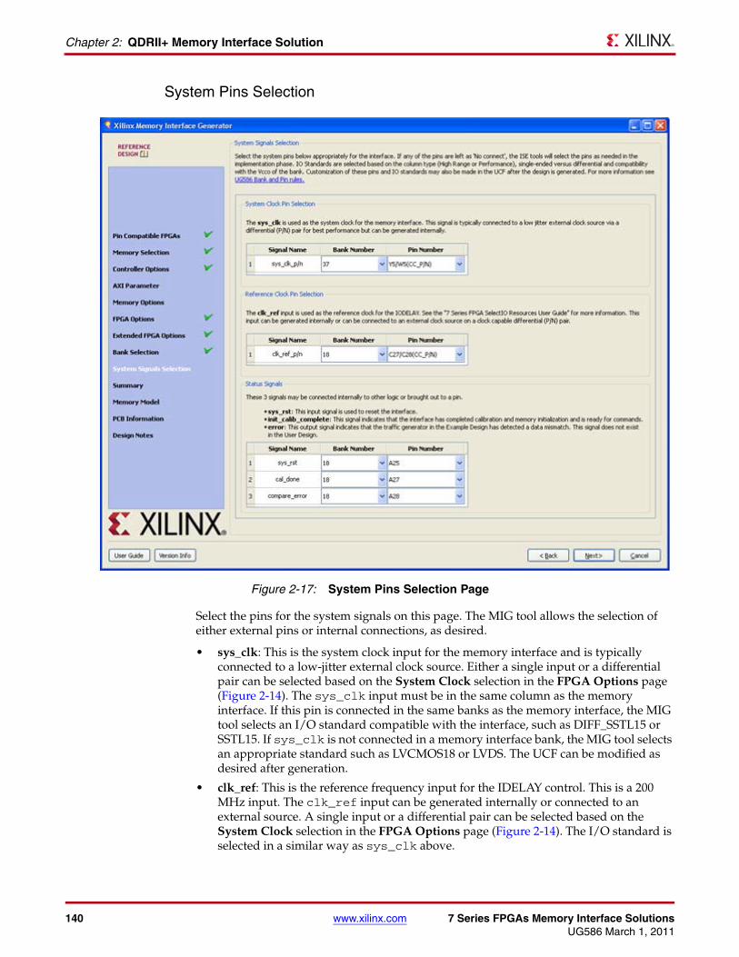
140 www.xilinx.com 7 Series FPGAs Memory Interface SolutionsUG586 March 1, 2011
Chapter 2: QDRII+ Memory Interface Solution
System Pins Selection
Select the pins for the system signals on this page. The MIG tool allows the selection of either external pins or internal connections, as desired.
• sys_clk: This is the system clock input for the memory interface and is typically connected to a low-jitter external clock source. Either a single input or a differential pair can be selected based on the System Clock selection in the FPGA Options page (Figure 2-14). The sys_clk input must be in the same column as the memory interface. If this pin is connected in the same banks as the memory interface, the MIG tool selects an I/O standard compatible with the interface, such as DIFF_SSTL15 or SSTL15. If sys_clk is not connected in a memory interface bank, the MIG tool selects an appropriate standard such as LVCMOS18 or LVDS. The UCF can be modified as desired after generation.
• clk_ref: This is the reference frequency input for the IDELAY control. This is a 200 MHz input. The clk_ref input can be generated internally or connected to an external source. A single input or a differential pair can be selected based on the System Clock selection in the FPGA Options page (Figure 2-14). The I/O standard is selected in a similar way as sys_clk above.
X-Ref Target - Figure 2-17
Figure 2-17: System Pins Selection Page
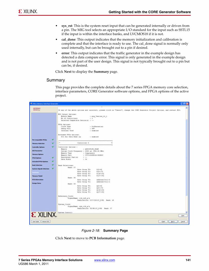
7 Series FPGAs Memory Interface Solutions www.xilinx.com 141UG586 March 1, 2011
Getting Started with the CORE Generator Software
• sys_rst: This is the system reset input that can be generated internally or driven from a pin. The MIG tool selects an appropriate I/O standard for the input such as SSTL15 if the input is within the interface banks, and LVCMOS18 if it is not.
• cal_done: This output indicates that the memory initialization and calibration is complete and that the interface is ready to use. The cal_done signal is normally only used internally, but can be brought out to a pin if desired.
• error: This output indicates that the traffic generator in the example design has detected a data compare error. This signal is only generated in the example design and is not part of the user design. This signal is not typically brought out to a pin but can be, if desired.
Click Next to display the Summary page.
Summary
This page provides the complete details about the 7 series FPGA memory core selection, interface parameters, CORE Generator software options, and FPGA options of the active project.
Click Next to move to PCB Information page.
X-Ref Target - Figure 2-18
Figure 2-18: Summary Page
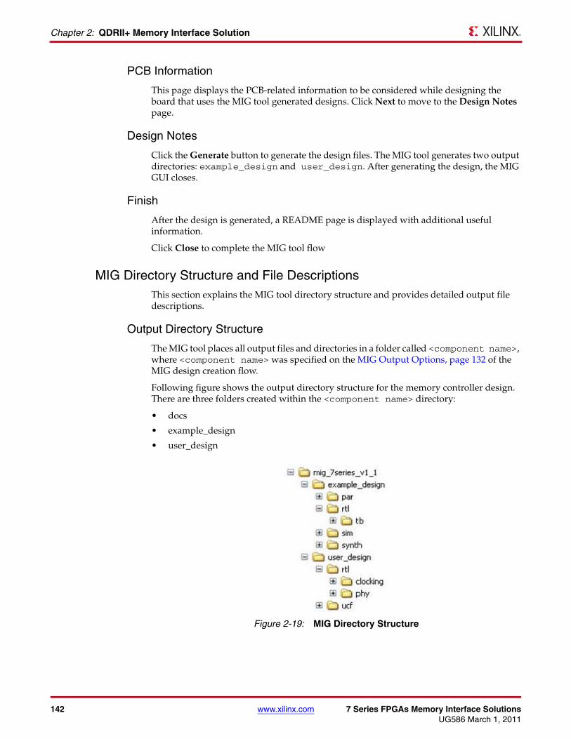
142 www.xilinx.com 7 Series FPGAs Memory Interface SolutionsUG586 March 1, 2011
Chapter 2: QDRII+ Memory Interface Solution
PCB Information
This page displays the PCB-related information to be considered while designing the board that uses the MIG tool generated designs. Click Next to move to the Design Notes page.
Design Notes
Click the Generate button to generate the design files. The MIG tool generates two output directories: example_design and user_design. After generating the design, the MIG GUI closes.
Finish
After the design is generated, a README page is displayed with additional useful information.
Click Close to complete the MIG tool flow
MIG Directory Structure and File DescriptionsThis section explains the MIG tool directory structure and provides detailed output file descriptions.
Output Directory Structure
The MIG tool places all output files and directories in a folder called <component name>, where <component name> was specified on the MIG Output Options, page 132 of the MIG design creation flow.
Following figure shows the output directory structure for the memory controller design. There are three folders created within the <component name> directory:
• docs
• example_design
• user_designX-Ref Target - Figure 2-19
Figure 2-19: MIG Directory Structure
7 Series FPGAs Memory Interface Solutions www.xilinx.com 143UG586 March 1, 2011
Getting Started with the CORE Generator Software
Directory and File Contents
The 7 series FPGAs core directories and their associated files are listed in this section.
<component name>/docs
The docs folder contains the PDF documentation.
<component name>/example_design/
The example_design directory structure contains all necessary RTL, constraints, and script files for simulation and implementation of the complete MIG example design with a test bench. The optional ChipScope™ tool module is also included in this directory structure.
Table 2-1 lists the files in the example_design/rtl directory
Table 2-2 lists the files in the example_design/rtl/tb directory
Table 2-3 lists the files in the example_design/sim directory
Table 2-4 lists the files in the example_design/par directory
Table 2-1: Files in example_design/rfl Directory
Name Description
example_top.v This top-level module serves as an example for connecting the user design to the 7 series FPGA memory interface core.
Table 2-2: Files in example_design/rfl/tb Directory
Name Description
tb_addr_gen.v Generates the write and read test memory addresses.
tb_cmp_data.v Generates the compare data and compares the write data against the captured read data.
tb_cmp_data_bits.v Incorporates a one bit comparison scheme.
tb_data_gen.v Generates test write data for the memory interface
tb_top.v Serves as the top level synthesizable user backend module
tb_wr_rd_sm.v generates writes and read commands emulating the user backend
Table 2-3: Files in example_design/sim Directory
Name Description
sim.do This is the ModelSim simulator script file.
sim_tb_top.v This file is the simulation top-level file.
144 www.xilinx.com 7 Series FPGAs Memory Interface SolutionsUG586 March 1, 2011
Chapter 2: QDRII+ Memory Interface Solution
Caution! The ise_flow.bat file in the par folder of the <component name> directory contains the recommended build options for the design. Failure to follow the recommended build options could produce unexpected results.
Table 2-5 lists the files in the example_design/synth directory
<component name>/user_design/
This directory contains the memory controller RTL files that are instantiated in the example design and a UCF.
Table 2-6 lists the files in the user_design/rtl directory
Table 2-7 lists the files in the user_design/rtl/clocking directory
Table 2-4: Files in the example_design/par Directory
Name Description
example_top.ucf This file is the UCF for the core of the example design.
create_ise.bat The user double-clicks this file to create an ISE tool project. The generated ISE tool project contains the recommended build options for the design. To run the project in GUI mode, the user double-clicks the ISE tool project file to open up the ISE tool in GUI mode with all project settings.
ise_flow.bat This script file runs the design through synthesis, build, map, and par. It sets all the required options. Users should refer to this file for the recommended build options for the design.
rem_files.bat Removes all the implementation files generated during implementation
set_ise_prop.tcl List of properties to ISE tool
xst_options.txt List of properties to synthesis tool
ila_cg.xco, icon_cg.xco, vio_cg.xco
XCO files for ChipScope modules to be generated when debug is enabled
Table 2-5: Files in the example_design/synth Directory
Name Description
example_top.prj Lists all the RTL files to be compiled by XST tool
Table 2-6: Files in the user_design/rtl Directory
Name Description
<component_name>.v This top level module servers as an example for connecting the user design to the 7 series FPGA QDRII+ SRAM memory interface core.
Table 2-7: Files in the user_design/rtl/clocking Directory
Name Description
infrastructure.v This module helps in clock generation and distribution.
clk_ibuf.v This module instantiates the system clock input buffers.
iodelay_ctrl.v This module instantiates the IDELAYCTRL primitive needed for IODELAY use.
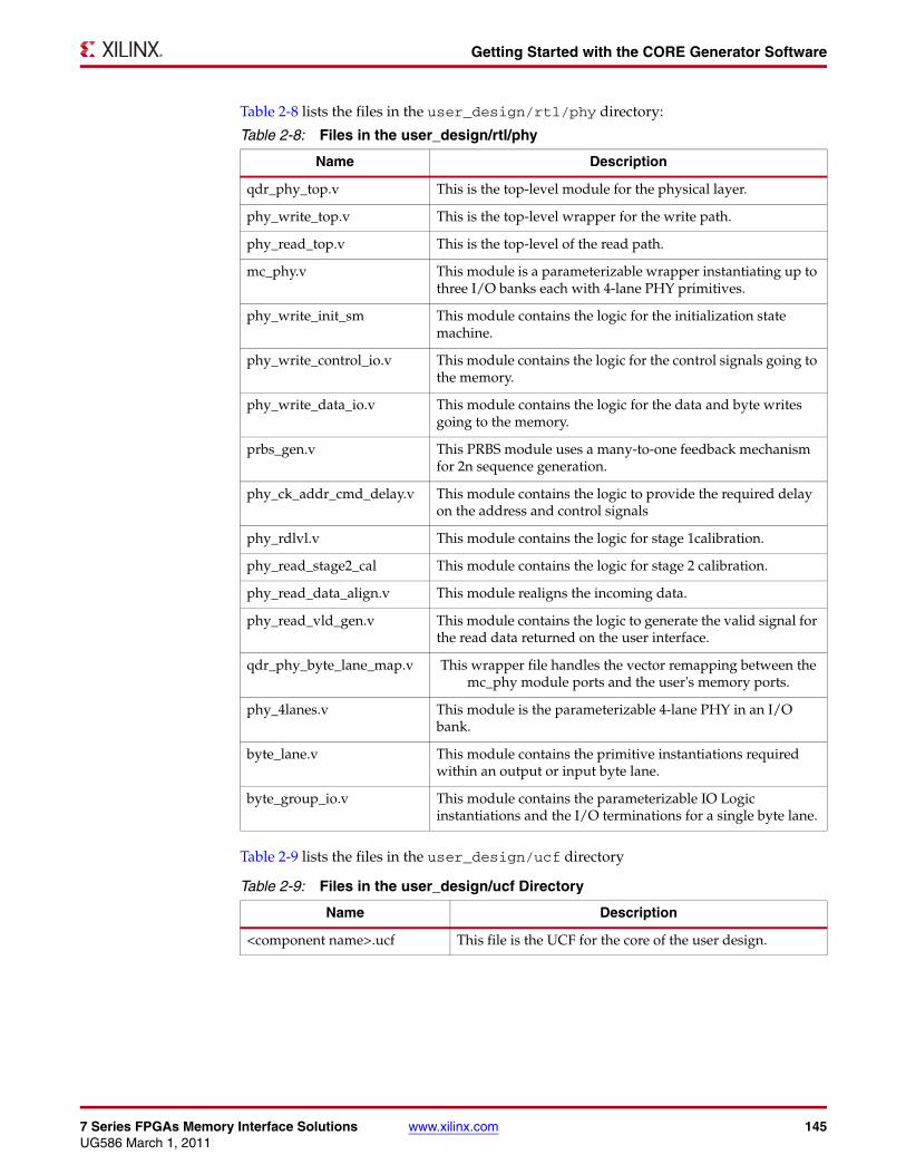
7 Series FPGAs Memory Interface Solutions www.xilinx.com 145UG586 March 1, 2011
Getting Started with the CORE Generator Software
Table 2-8 lists the files in the user_design/rtl/phy directory:
Table 2-9 lists the files in the user_design/ucf directory
Table 2-8: Files in the user_design/rtl/phy
Name Description
qdr_phy_top.v This is the top-level module for the physical layer.
phy_write_top.v This is the top-level wrapper for the write path.
phy_read_top.v This is the top-level of the read path.
mc_phy.v This module is a parameterizable wrapper instantiating up to three I/O banks each with 4-lane PHY primitives.
phy_write_init_sm This module contains the logic for the initialization state machine.
phy_write_control_io.v This module contains the logic for the control signals going to the memory.
phy_write_data_io.v This module contains the logic for the data and byte writes going to the memory.
prbs_gen.v This PRBS module uses a many-to-one feedback mechanism for 2n sequence generation.
phy_ck_addr_cmd_delay.v This module contains the logic to provide the required delay on the address and control signals
phy_rdlvl.v This module contains the logic for stage 1calibration.
phy_read_stage2_cal This module contains the logic for stage 2 calibration.
phy_read_data_align.v This module realigns the incoming data.
phy_read_vld_gen.v This module contains the logic to generate the valid signal for the read data returned on the user interface.
qdr_phy_byte_lane_map.v This wrapper file handles the vector remapping between the mc_phy module ports and the user's memory ports.
phy_4lanes.v This module is the parameterizable 4-lane PHY in an I/O bank.
byte_lane.v This module contains the primitive instantiations required within an output or input byte lane.
byte_group_io.v This module contains the parameterizable IO Logic instantiations and the I/O terminations for a single byte lane.
Table 2-9: Files in the user_design/ucf Directory
Name Description
<component name>.ucf This file is the UCF for the core of the user design.
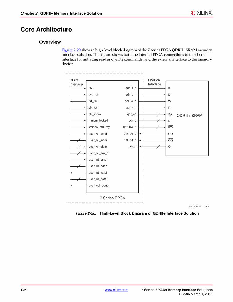
146 www.xilinx.com 7 Series FPGAs Memory Interface SolutionsUG586 March 1, 2011
Chapter 2: QDRII+ Memory Interface Solution
Core Architecture
OverviewFigure 2-20 shows a high-level block diagram of the 7 series FPGA QDRII+ SRAM memory interface solution. This figure shows both the internal FPGA connections to the client interface for initiating read and write commands, and the external interface to the memory device.X-Ref Target - Figure 2-20
Figure 2-20: High-Level Block Diagram of QDRII+ Interface Solution
UG586_c2_34_012411
K
K
W
R
SA
D
BW
Q
PhysicalInterface
ClientInterface
qdr_bw_n
qdr_cq_p
qdr_cq_n
qdr_q
clk
sys_rst
rst_dk
clk_wr
clk_mem
mmcm_locked
iodelay_ctrl_rdy
CQ
QDR II+ SRAM
7 Series FPGA
CQ
qdr_k_p
qdr_k_n
qdr_w_n
qdr_r_n
qdr_sa
qdr_d
user_wr_cmd
user_wr_addr
user_wr_data
user_wr_bw_n
user_rd_cmd
user_rd_addr
user_rd_valid
user_rd_data
user_cal_done
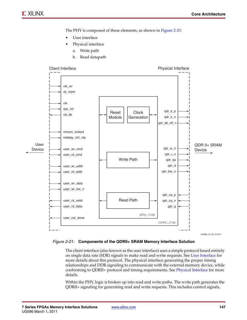
7 Series FPGAs Memory Interface Solutions www.xilinx.com 147UG586 March 1, 2011
Core Architecture
The PHY is composed of these elements, as shown in Figure 2-21:
• User interface
• Physical interface
a. Write path
b. Read datapath
The client interface (also known as the user interface) uses a simple protocol based entirely on single data rate (SDR) signals to make read and write requests. See User Interface for more details about this protocol. The physical interface generating the proper timing relationships and DDR signaling to communicate with the external memory device, while conforming to QDRII+ protocol and timing requirements. See Physical Interface for more details.
Within the PHY, logic is broken up into read and write paths. The write path generates the QDRII+ signaling for generating read and write requests. This includes control signals,
X-Ref Target - Figure 2-21
Figure 2-21: Components of the QDRII+ SRAM Memory Interface Solution
UG586_c2_35_012411
Client Interface
UserDevice
Physical Interface
clk_wr
ck_mem
clk
sys_rstqdr_k_p
qdr_k_nReset
Modulerst_dk
mmcm_locked
iodelay_ctrl_rdy
user_wr_cmd
user_rd_cmd
user_wr_addr
user_rd_addr
user_wr_data
user_wr_bw_n
user_rd_valid
user_cal_done
user_rd_data
QDR II+ SRAMDevice
Read Path
phy_top
user_top
Write Path
ClockGeneration
qdr_w_n
qdr_r_n
qdr_sa
qdr_d
qdr_bw_n
qdr_cq_p
qdr_cq_n
qdr_q
qdr_dll_off_n
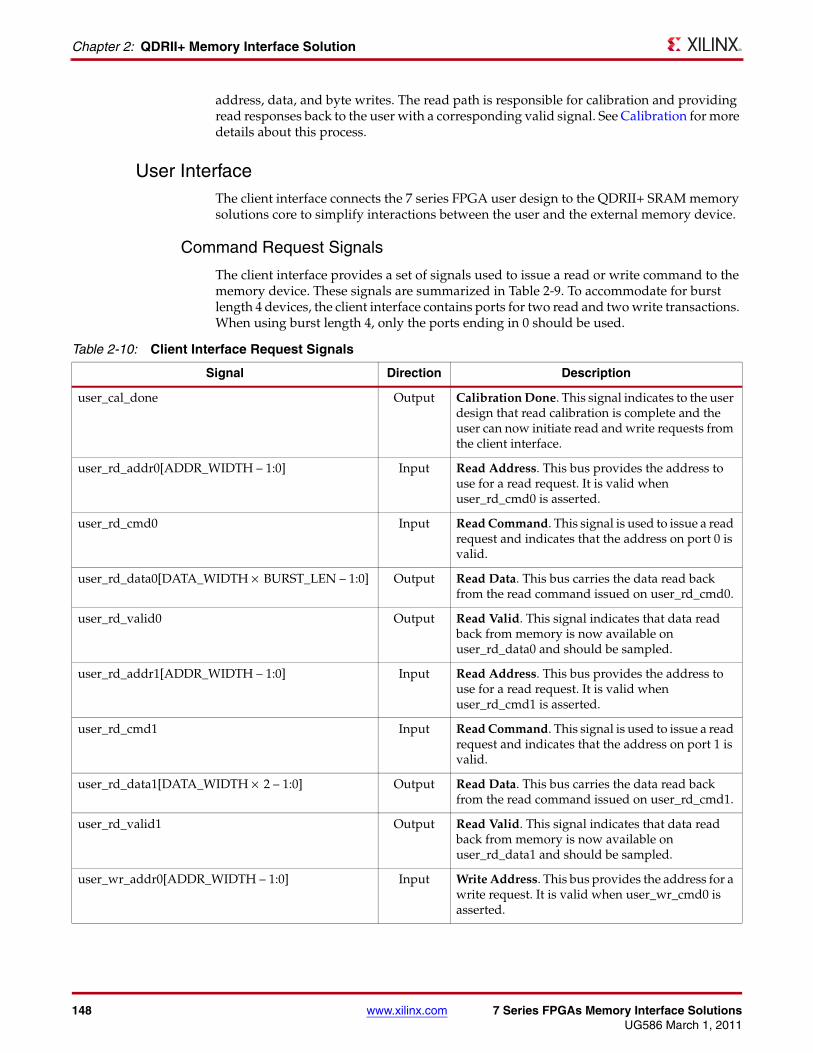
148 www.xilinx.com 7 Series FPGAs Memory Interface SolutionsUG586 March 1, 2011
Chapter 2: QDRII+ Memory Interface Solution
address, data, and byte writes. The read path is responsible for calibration and providing read responses back to the user with a corresponding valid signal. See Calibration for more details about this process.
User InterfaceThe client interface connects the 7 series FPGA user design to the QDRII+ SRAM memory solutions core to simplify interactions between the user and the external memory device.
Command Request Signals
The client interface provides a set of signals used to issue a read or write command to the memory device. These signals are summarized in Table 2-9. To accommodate for burst length 4 devices, the client interface contains ports for two read and two write transactions. When using burst length 4, only the ports ending in 0 should be used.
Table 2-10: Client Interface Request Signals
Signal Direction Description
user_cal_done Output Calibration Done. This signal indicates to the user design that read calibration is complete and the user can now initiate read and write requests from the client interface.
user_rd_addr0[ADDR_WIDTH – 1:0] Input Read Address. This bus provides the address to use for a read request. It is valid when user_rd_cmd0 is asserted.
user_rd_cmd0 Input Read Command. This signal is used to issue a read request and indicates that the address on port 0 is valid.
user_rd_data0[DATA_WIDTH × BURST_LEN – 1:0] Output Read Data. This bus carries the data read back from the read command issued on user_rd_cmd0.
user_rd_valid0 Output Read Valid. This signal indicates that data read back from memory is now available on user_rd_data0 and should be sampled.
user_rd_addr1[ADDR_WIDTH – 1:0] Input Read Address. This bus provides the address to use for a read request. It is valid when user_rd_cmd1 is asserted.
user_rd_cmd1 Input Read Command. This signal is used to issue a read request and indicates that the address on port 1 is valid.
user_rd_data1[DATA_WIDTH × 2 – 1:0] Output Read Data. This bus carries the data read back from the read command issued on user_rd_cmd1.
user_rd_valid1 Output Read Valid. This signal indicates that data read back from memory is now available on user_rd_data1 and should be sampled.
user_wr_addr0[ADDR_WIDTH – 1:0] Input Write Address. This bus provides the address for a write request. It is valid when user_wr_cmd0 is asserted.
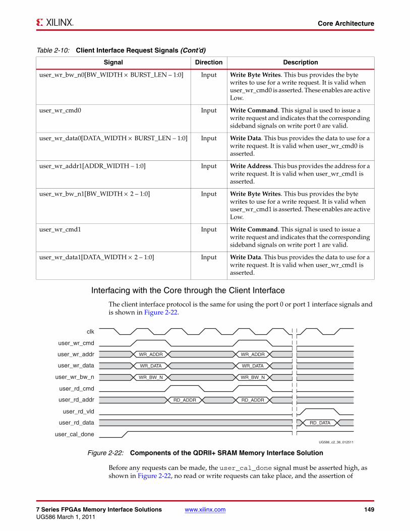
7 Series FPGAs Memory Interface Solutions www.xilinx.com 149UG586 March 1, 2011
Core Architecture
Interfacing with the Core through the Client Interface
The client interface protocol is the same for using the port 0 or port 1 interface signals and is shown in Figure 2-22.
Before any requests can be made, the user_cal_done signal must be asserted high, as shown in Figure 2-22, no read or write requests can take place, and the assertion of
user_wr_bw_n0[BW_WIDTH × BURST_LEN – 1:0] Input Write Byte Writes. This bus provides the byte writes to use for a write request. It is valid when user_wr_cmd0 is asserted. These enables are active Low.
user_wr_cmd0 Input Write Command. This signal is used to issue a write request and indicates that the corresponding sideband signals on write port 0 are valid.
user_wr_data0[DATA_WIDTH × BURST_LEN – 1:0] Input Write Data. This bus provides the data to use for a write request. It is valid when user_wr_cmd0 is asserted.
user_wr_addr1[ADDR_WIDTH – 1:0] Input Write Address. This bus provides the address for a write request. It is valid when user_wr_cmd1 is asserted.
user_wr_bw_n1[BW_WIDTH × 2 – 1:0] Input Write Byte Writes. This bus provides the byte writes to use for a write request. It is valid when user_wr_cmd1 is asserted. These enables are active Low.
user_wr_cmd1 Input Write Command. This signal is used to issue a write request and indicates that the corresponding sideband signals on write port 1 are valid.
user_wr_data1[DATA_WIDTH × 2 – 1:0] Input Write Data. This bus provides the data to use for a write request. It is valid when user_wr_cmd1 is asserted.
Table 2-10: Client Interface Request Signals (Cont’d)
Signal Direction Description
X-Ref Target - Figure 2-22
Figure 2-22: Components of the QDRII+ SRAM Memory Interface Solution
UG586_c2_36_012511
user_wr_cmd
user_wr_addr
user_wr_data
user_wr_bw_n
user_rd_cmd
user_rd_addr
user_rd_data
user_cal_done
user_rd_vld
clk
WR_ADDR WR_ADDR
WR_DATA WR_DATA
WR_BW_N WR_BW_N
RD_ADDR RD_ADDR
RD_DATA
150 www.xilinx.com 7 Series FPGAs Memory Interface SolutionsUG586 March 1, 2011
Chapter 2: QDRII+ Memory Interface Solution
user_wr_cmd or user_rd_cmd on the client interface is ignored. A write request is issued by asserting user_wr_cmd as a single cycle pulse. At this time, the user_wr_addr, user_wr_data, and user_wr_bw_n signals must be valid. On the following cycle, a read request is issued by asserting user_rd_cmd for a single cycle pulse. At this time, user_rd_addr must be valid. After one cycle of idle time, a read and write request are both asserted on the same clock cycle. In this case, the read to the memory occurs first, followed by the write.
Figure 2-22 also shows data returning from the memory device to the user design. The user_rd_vld signal is asserted, indicating that user_rd_data is now valid. This should be sampled on the same cycle that user_rd_vld is asserted because the core does not buffer returning data. This functionality can be added in by the user, if desired. The data returned is not necessarily from the read commands shown in Figure 2-22 and is solely to demonstrate protocol.
Clocking ArchitectureThe PHY design requires that a PLL module be used to generate various clocks. Both global and local clock networks are used to distribute the clock throughout the design.
The clock generation and distribution circuitry and networks drive blocks within the PHY that can be divided roughly into four separate general functions:
• Internal FPGA logic
• Write path (output) logic
• Read path (input) and delay logic
• IDELAY reference clock (200 MHz)
One PLL is required for the PHY. The PLL is used to generate the clocks for most of the internal logic, the input clocks to the phasers, and a synchronization pulse required to keep the PHASER blocks synchronized in a multi-I/O bank implementation.
The PHASER blocks require 3 clocks, a memory reference clock, a frequency reference clock and a phase reference clock from the PLL. The memory reference clock is required to be at the same frequency as that of the QDRII+ memory interface clock. The frequency reference clock must be either 2x or 4x the memory clock frequency such that it meets the frequency range requirement of 400 MHz to 1066 MHz. The phase reference clock is used in the read banks, and is generated using the memory read clock (CQ/CQ#) routed internally and provided to the Phaser logic to assist with data capture.
The internal fabric clock generated by the PLL is clocked by a global clocking resource at half the frequency of the QDII+ memory frequency.
A 200 MHz IDELAY reference clock must be supplied to the IDELAYCTRL module. The IDELAYCTRL module continuously calibrates the IDELAY elements in the I/O region to account for varying environmental conditions. The IP core assumes an external clock signal is driving the IDELAYCTRL module. If a PLL clock drives the IDELAYCTRL input clock, the PLL lock signal needs to be incorporated in the rst_tmp_idelay signal inside the IODELAY_CTRL module. This ensures that the clock is stable before being used.
Table 2-11 lists the signals used in the infrastructure module that provides the necessary clocks and reset signals required in the design.
7 Series FPGAs Memory Interface Solutions www.xilinx.com 151UG586 March 1, 2011
Core Architecture
Physical InterfaceThe physical interface is the connection from the FPGA memory interface solution to an external QDRII+ SRAM device. The I/O signals for this interface are shown in Table 2-12. These signals can be directly connected to the corresponding signals on the QDRII+ SRAM device.
Table 2-11: Infrastructure clocking and reset signals
Signal Direction Description
mmcm_clk Input System clock input
sys_rst Input Core reset from user application
iodelay_ctrl_rdy Input IDELAYCTRL lock status
clk Output Half frequency fabric clock
mem_refclk Output PLL output clock at same frequency as the memory clock
freq_refclk Output PLL output clock to provide the FREQREFCLK input to the Phaser. The freq_refclk is generated such that its frequency in the range of 400 MHz - 1066 MHz
sync_pulse Output PLL output generated at 1/16 of mem_Refclk and is a synchronization signal sent to the PHY Hard blocks that are used in a multi-bank implementation
pll_locked Output Locked output from PLLE2_ADV
rstdiv0 Output Reset output synchronized to internal fabric half frequency clock.
Table 2-12: Physical Interface Signals
Signal Direction Description
qdr_cq_n Input QDR CQ#. This is the echo clock returned from the memory derived from qdr_k_n.
qdr_cq_p Input QDR CQ. This is the echo clock returned from the memory derived from qdr_k_p.
qdr_d Output QDR Data. This is the write data from the PHY to the QDR II+ memory device.
qdr_dll_off_n Output QDR DLL Off. This signal turns off the DLL in the memory device.
qdr_bw_n Output QDR Byte Write. This is the byte write signal from the PHY to the QDRII+ SRAM device.
qdr_k_n Output QDR Clock K#. This is the inverted input clock to the memory device.
qdr_k_p Output QDR Clock K. This is the input clock to the memory device.
qdr_q Input QDR Data Q. This is the data returned from reads to memory.

152 www.xilinx.com 7 Series FPGAs Memory Interface SolutionsUG586 March 1, 2011
Chapter 2: QDRII+ Memory Interface Solution
Interfacing with the Memory Device
Figure 2-23 shows the physical interface protocol for a four-word memory device.
In four-word burst mode:
• The address is in SDR format
• All signals as input to the memory are center aligned with respect to qdr_k_p
• The data for a write request follows on the next rising edge of qdr_k_p after an assertion of qdr_w_n
• Byte writes are sampled along with data
• The qdr_qvld signal is asserted half a cycle before the return of data edge aligned to the qdr_cq_n clock
• The qdr_q signal is edge aligned to qdr_cq_p and qdr_cq_n
qdr_qvld Input QDR Q Valid. This signal indicates that the data on qdr_q is valid. It is only present in QDRII+ SRAM devices.
qdr_sa Output QDR Address. This is the address supplied for memory operations.
qdr_w_n Output QDR Write. This is the write command to memory.
qdr_r_n Output QDR Read. This is the read command to memory.
Table 2-12: Physical Interface Signals (Cont’d)
Signal Direction Description
X-Ref Target - Figure 2-23
Figure 2-23: Four-Word Burst Length Memory Device Protocol
UG586_c2_37_012511
qdr_k_n
qdr_w_n
qdr_r_n
qdr_sa
qdr_d
qdr_bw_n
qdr_q
qdr_k_p
RD_ADDR WR_ADDR
DW1 DW2 DW3 DW4
DW1 DW2 DW3 DW4
BW1 BW2 BW3 BW4
qdr_cq_n
qdr_qvld
qdr_cq_p
7 Series FPGAs Memory Interface Solutions www.xilinx.com 153UG586 March 1, 2011
Core Architecture
PHY Architecture
The 7 series FPGA PHY is composed of dedicated blocks and soft calibration logic. The dedicated blocks are structured adjacent to one another with back-to-back interconnects to minimize the clock and datapath routing necessary to build high-performance physical layers.
Some of the dedicated blocks that are used in the QDRII+ SRAM PHY and their features are described below:
• I/Os available within each 7 series bank are grouped into four byte groups, where each byte group consists of up to 12 I/Os.
• PHASER_IN/PHASER_OUT blocks are available in each byte group and are multi-stage programmable delay line loops that can provide precision phase adjustment of the clocks. Dedicated clock structures within an I/O bank referred to as byte group clocks generated by the PHASERs help minimize the number of loads driven by the byte group clock drivers.
• OUT_FIFO and IN_FIFO are shallow 8-deep FIFOs available in each byte group and serve to transfer data from the fabric domain to the I/O clock domain. OUT_FIFOs are used to store output data and address/controls that need to sent to the memory while IN_FIFOs are used to store captured read data before transfer to the fabric.
The Pinout Requirements section explains the rules that need to be followed while placing the memory interface signals inside the byte groups.
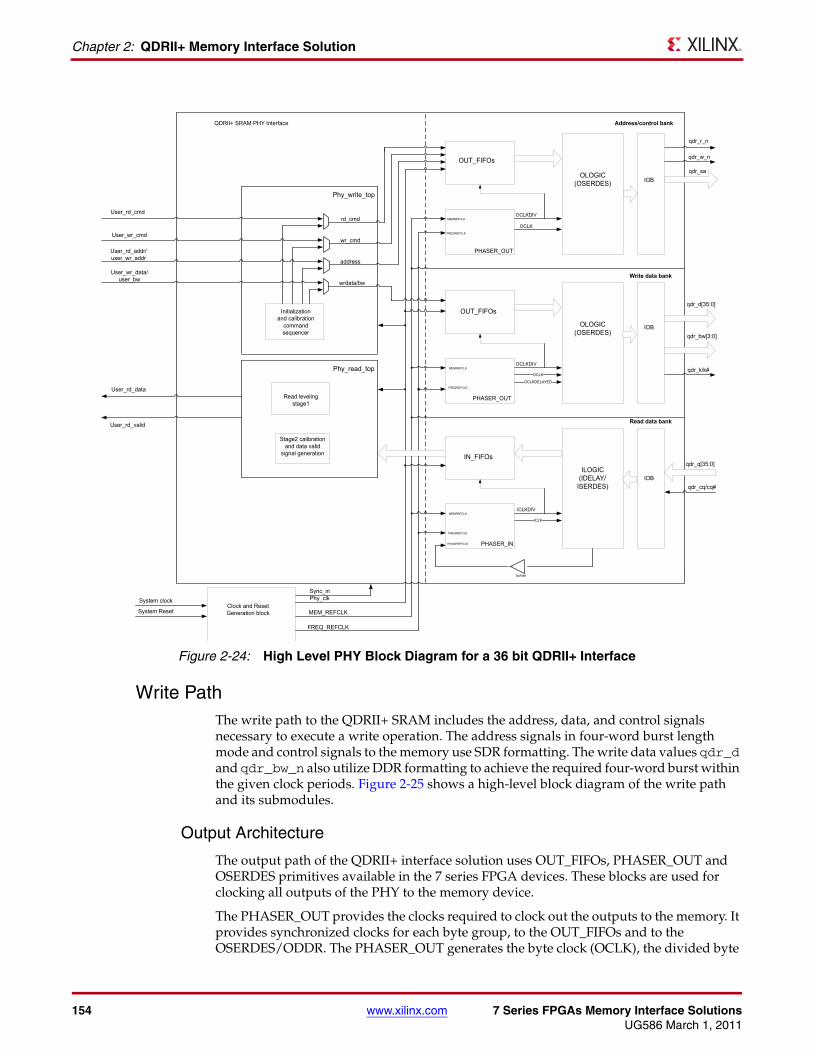
154 www.xilinx.com 7 Series FPGAs Memory Interface SolutionsUG586 March 1, 2011
Chapter 2: QDRII+ Memory Interface Solution
Write PathThe write path to the QDRII+ SRAM includes the address, data, and control signals necessary to execute a write operation. The address signals in four-word burst length mode and control signals to the memory use SDR formatting. The write data values qdr_d and qdr_bw_n also utilize DDR formatting to achieve the required four-word burst within the given clock periods. Figure 2-25 shows a high-level block diagram of the write path and its submodules.
Output Architecture
The output path of the QDRII+ interface solution uses OUT_FIFOs, PHASER_OUT and OSERDES primitives available in the 7 series FPGA devices. These blocks are used for clocking all outputs of the PHY to the memory device.
The PHASER_OUT provides the clocks required to clock out the outputs to the memory. It provides synchronized clocks for each byte group, to the OUT_FIFOs and to the OSERDES/ODDR. The PHASER_OUT generates the byte clock (OCLK), the divided byte
X-Ref Target - Figure 2-24
Figure 2-24: High Level PHY Block Diagram for a 36 bit QDRII+ Interface
#������'������������&�������������(�������
)��� ��������
����������
����� ����
������������*����� ������
����� ������*������&
������������ ���
+�$�,#,+�
)-�.%��+�$
+/+0#1��+.%�2%.�
������������������3
)�����������
1���"����������0��������&���"
.����)�����"
�%���%,1/4
,�%5��%,1/4
�����
����
�������
�����*&
+1/42#6
+1/4
+�$�,#,+�
)-�.%��+�$
+/+0#1��+.%�2%.�
+1/4
+1/42#6
�%��%,1/4
,�%5�%,1/4
�%��%,1/4
,�%5�%,1/4
+1/42%/�7%2
#+8
#+8
#9�,#,+�
)-�.%��#9
#/+0#1��#2%/�7*�#.%�2%.�
#1/4
#1/42#6�%��%,1/4
,�%5�%,1/4
#+8
.����:�����&����������������������������������
�������������
������������
����� ���� ���
���� ���� ���
(�����
(��� �
(�����
(����;<=>�?
(���& ;<>�?
(���"*"@
(���(;<=>�?
(����(*�(@
.���������"
.����������
52�##A�.����)-7�#�������
������
)-�.%�%,1/4
8�,��
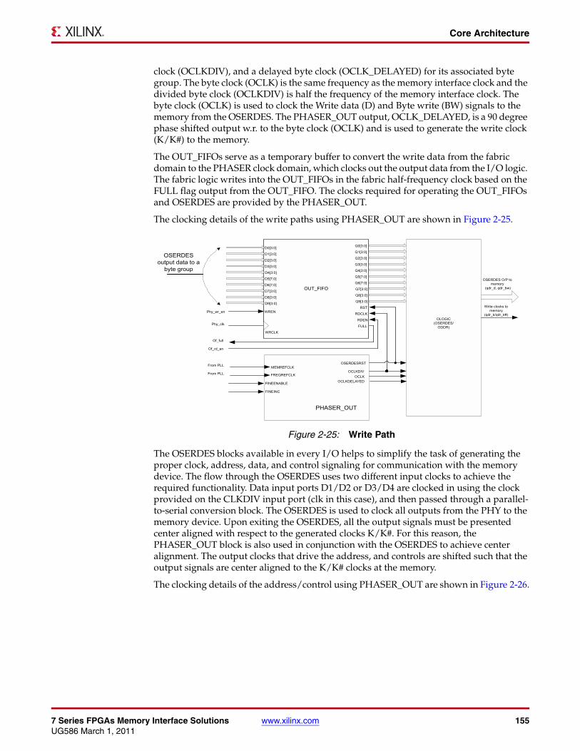
7 Series FPGAs Memory Interface Solutions www.xilinx.com 155UG586 March 1, 2011
Core Architecture
clock (OCLKDIV), and a delayed byte clock (OCLK_DELAYED) for its associated byte group. The byte clock (OCLK) is the same frequency as the memory interface clock and the divided byte clock (OCLKDIV) is half the frequency of the memory interface clock. The byte clock (OCLK) is used to clock the Write data (D) and Byte write (BW) signals to the memory from the OSERDES. The PHASER_OUT output, OCLK_DELAYED, is a 90 degree phase shifted output w.r. to the byte clock (OCLK) and is used to generate the write clock (K/K#) to the memory.
The OUT_FIFOs serve as a temporary buffer to convert the write data from the fabric domain to the PHASER clock domain, which clocks out the output data from the I/O logic. The fabric logic writes into the OUT_FIFOs in the fabric half-frequency clock based on the FULL flag output from the OUT_FIFO. The clocks required for operating the OUT_FIFOs and OSERDES are provided by the PHASER_OUT.
The clocking details of the write paths using PHASER_OUT are shown in Figure 2-25.
The OSERDES blocks available in every I/O helps to simplify the task of generating the proper clock, address, data, and control signaling for communication with the memory device. The flow through the OSERDES uses two different input clocks to achieve the required functionality. Data input ports D1/D2 or D3/D4 are clocked in using the clock provided on the CLKDIV input port (clk in this case), and then passed through a parallel-to-serial conversion block. The OSERDES is used to clock all outputs from the PHY to the memory device. Upon exiting the OSERDES, all the output signals must be presented center aligned with respect to the generated clocks K/K#. For this reason, the PHASER_OUT block is also used in conjunction with the OSERDES to achieve center alignment. The output clocks that drive the address, and controls are shifted such that the output signals are center aligned to the K/K# clocks at the memory.
The clocking details of the address/control using PHASER_OUT are shown in Figure 2-26.
X-Ref Target - Figure 2-25
Figure 2-25: Write Path
+�$�,#,+
2B;<>�?�.$
!�1/4��
�21/4��
�2%9
,�//
2�;<>�?
23;<>�?
2:;<>�?
2<;<>�?
2C;<>�?������
2=;D>�?
2E;D>�?
2D;<>�?
2F;<>�?
������
!�%9
5B;<>�?
5�;<>�?
53;<>�?
5:;<>�?
5<;<>�?
5C;<>�?
5=;D>�?
5E;D>�?
5D;<>�?
5F;<>�?
�%��%,1/4
,�%5�%,1/4
,#9%%9�8/%
,#9%#91
+1/42#6+1/4
+1/42%/�7%2
+.%�2%.�.$
+/+0#1��+.%�2%.*+22��
+.%�2%.������������������&���������
)��� ���
)�����"
+������
+������
,���)//
,���)//
)-�.%��+�$
!���������"����������
�(���"*(���"@�
+.%�2%.�+*)��������
��(����G�(���& �
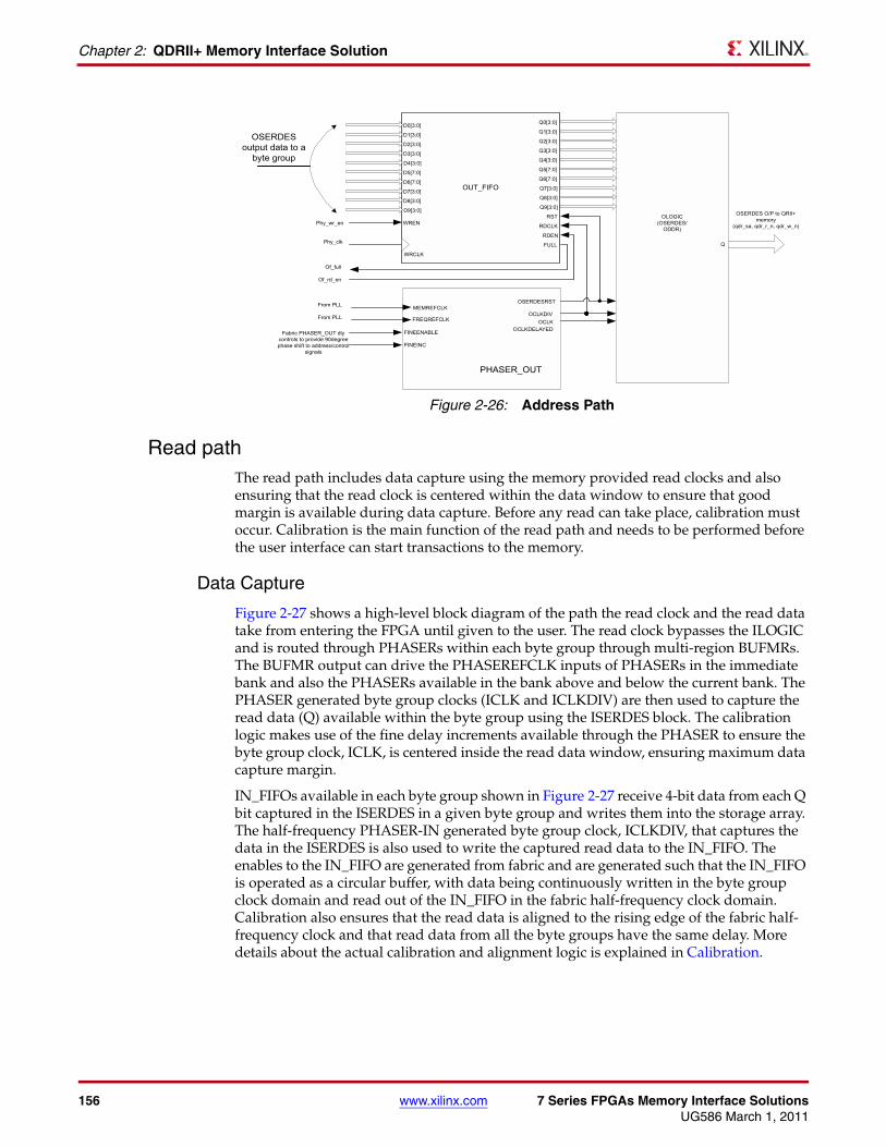
156 www.xilinx.com 7 Series FPGAs Memory Interface SolutionsUG586 March 1, 2011
Chapter 2: QDRII+ Memory Interface Solution
Read path The read path includes data capture using the memory provided read clocks and also ensuring that the read clock is centered within the data window to ensure that good margin is available during data capture. Before any read can take place, calibration must occur. Calibration is the main function of the read path and needs to be performed before the user interface can start transactions to the memory.
Data Capture
Figure 2-27 shows a high-level block diagram of the path the read clock and the read data take from entering the FPGA until given to the user. The read clock bypasses the ILOGIC and is routed through PHASERs within each byte group through multi-region BUFMRs. The BUFMR output can drive the PHASEREFCLK inputs of PHASERs in the immediate bank and also the PHASERs available in the bank above and below the current bank. The PHASER generated byte group clocks (ICLK and ICLKDIV) are then used to capture the read data (Q) available within the byte group using the ISERDES block. The calibration logic makes use of the fine delay increments available through the PHASER to ensure the byte group clock, ICLK, is centered inside the read data window, ensuring maximum data capture margin.
IN_FIFOs available in each byte group shown in Figure 2-27 receive 4-bit data from each Q bit captured in the ISERDES in a given byte group and writes them into the storage array. The half-frequency PHASER-IN generated byte group clock, ICLKDIV, that captures the data in the ISERDES is also used to write the captured read data to the IN_FIFO. The enables to the IN_FIFO are generated from fabric and are generated such that the IN_FIFO is operated as a circular buffer, with data being continuously written in the byte group clock domain and read out of the IN_FIFO in the fabric half-frequency clock domain. Calibration also ensures that the read data is aligned to the rising edge of the fabric half-frequency clock and that read data from all the byte groups have the same delay. More details about the actual calibration and alignment logic is explained in Calibration.
X-Ref Target - Figure 2-26
Figure 2-26: Address Path
+�$�,#,+
2B;<>�?�.$
!�1/4��
�21/4��
�2%9
,�//
2�;<>�?
23;<>�?
2:;<>�?
2<;<>�?
2C;<>�?������
2=;D>�?
2E;D>�?
2D;<>�?
2F;<>�?
������
!�%9
5B;<>�?
5�;<>�?
53;<>�?
5:;<>�?
5<;<>�?
5C;<>�?
5=;D>�?
5E;D>�?
5D;<>�?
5F;<>�?
�%��%,1/4
,�%5�%,1/4
,#9%%9�8/%
,#9%#91
+1/42#6+1/4
+1/42%/�7%2
+.%�2%.�.$
+/+0#1��+.%�2%.*+22��
5
+.%�2%.������������������&���������
)��� ���
)�����"
+������
+������
,���)//
,���)//
,�&����)-�.%��+�$������������������������B������������������������������*�������
������
)-�.%��+�$
+.%�2%.�+*)����5�##A�����
�(�����G�(�����G�(��� ����
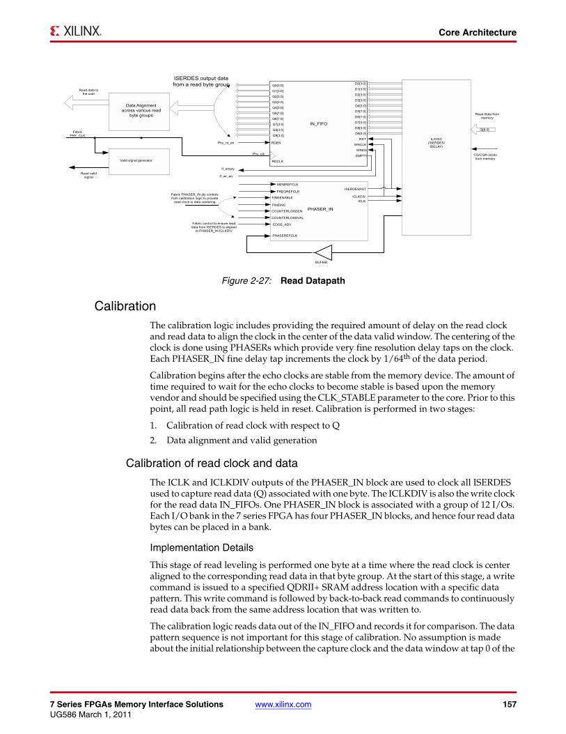
7 Series FPGAs Memory Interface Solutions www.xilinx.com 157UG586 March 1, 2011
Core Architecture
CalibrationThe calibration logic includes providing the required amount of delay on the read clock and read data to align the clock in the center of the data valid window. The centering of the clock is done using PHASERs which provide very fine resolution delay taps on the clock. Each PHASER_IN fine delay tap increments the clock by 1/64th of the data period.
Calibration begins after the echo clocks are stable from the memory device. The amount of time required to wait for the echo clocks to become stable is based upon the memory vendor and should be specified using the CLK_STABLE parameter to the core. Prior to this point, all read path logic is held in reset. Calibration is performed in two stages:
1. Calibration of read clock with respect to Q
2. Data alignment and valid generation
Calibration of read clock and data
The ICLK and ICLKDIV outputs of the PHASER_IN block are used to clock all ISERDES used to capture read data (Q) associated with one byte. The ICLKDIV is also the write clock for the read data IN_FIFOs. One PHASER_IN block is associated with a group of 12 I/Os. Each I/O bank in the 7 series FPGA has four PHASER_IN blocks, and hence four read data bytes can be placed in a bank.
Implementation Details
This stage of read leveling is performed one byte at a time where the read clock is center aligned to the corresponding read data in that byte group. At the start of this stage, a write command is issued to a specified QDRII+ SRAM address location with a specific data pattern. This write command is followed by back-to-back read commands to continuously read data back from the same address location that was written to.
The calibration logic reads data out of the IN_FIFO and records it for comparison. The data pattern sequence is not important for this stage of calibration. No assumption is made about the initial relationship between the capture clock and the data window at tap 0 of the
X-Ref Target - Figure 2-27
Figure 2-27: Read Datapath
#9�,#,+
2B;<>�?
�.$
�21/4
!�1/4��
!�%9
%�)$7
2�;<>�?
23;<>�?
2:;<>�?
2<;<>�?
2C;<>�?������
2=;D>�?
2E;D>�?
2D;<>�?
2F;<>�?
������
�2%9
5B;<>�?
5�;<>�?
53;<>�?
5:;<>�?
5<;<>�?
5C;<>�?
5=;D>�?
5E;D>�?
5D;<>�?
5F;<>�?
�%��%,1/4
,�%5�%,1/4
,#9%%9�8/%
,#9%#91
1+�9$%�/+�2%9
1+�9$%�/+�26�/
#1/42#6#1/4
#.%�2%.�.$
#/+0#1�#.%�2%.*#2%/�7�
5;F>�?
#.%�2%.������������������������&���������
)�������
)�����"
#������
#�� ���
������
)-�.%�%,1/4
,�&����)-�.%��#9���������������������&��������������������������������"������������������
)-�.%��#9
%20%��26,�&����������������������������������#.%�2%.��������������)-�.%��#9�#1/42#6
2�������������������������������
&����������
6�������������������
,�&����)-7�1/4
���������������������
����������������
�����2������������
8�,��
15*15@�����"����������
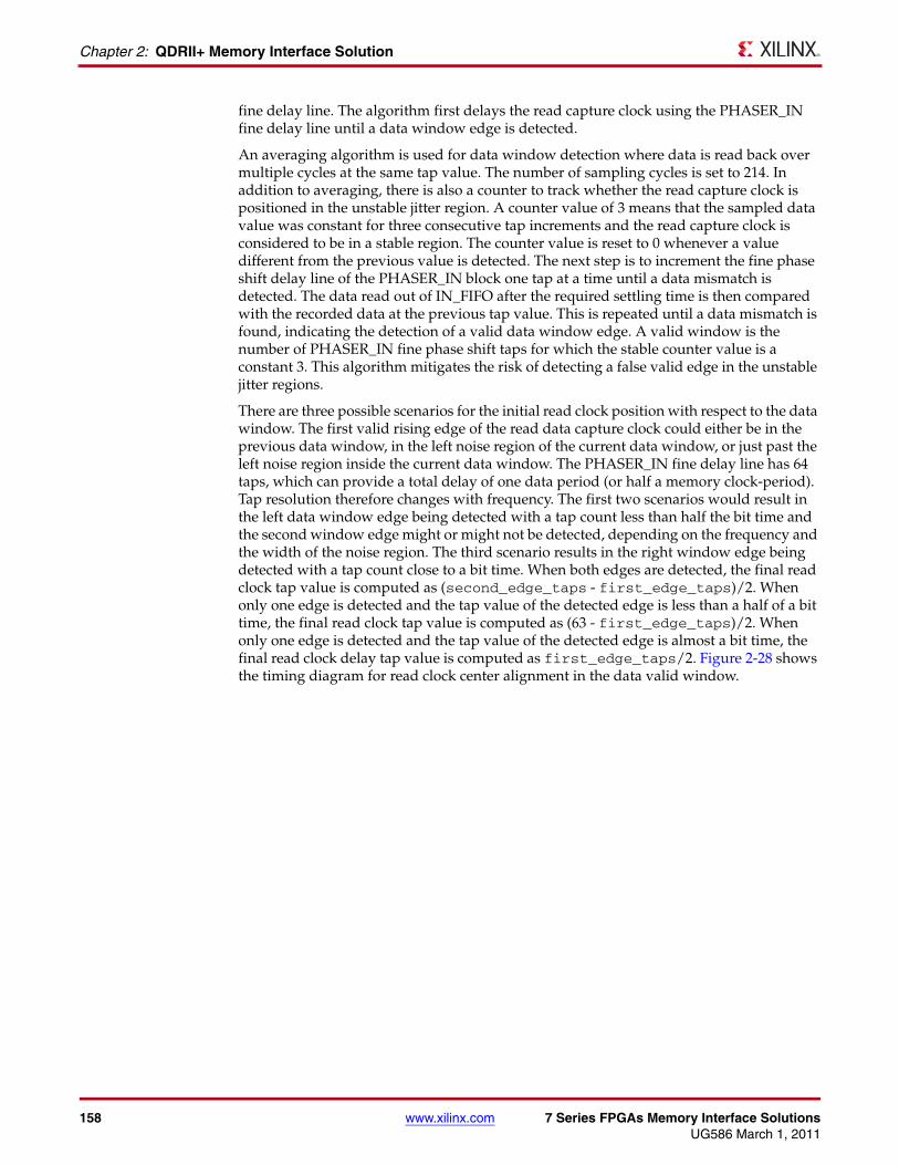
158 www.xilinx.com 7 Series FPGAs Memory Interface SolutionsUG586 March 1, 2011
Chapter 2: QDRII+ Memory Interface Solution
fine delay line. The algorithm first delays the read capture clock using the PHASER_IN fine delay line until a data window edge is detected.
An averaging algorithm is used for data window detection where data is read back over multiple cycles at the same tap value. The number of sampling cycles is set to 214. In addition to averaging, there is also a counter to track whether the read capture clock is positioned in the unstable jitter region. A counter value of 3 means that the sampled data value was constant for three consecutive tap increments and the read capture clock is considered to be in a stable region. The counter value is reset to 0 whenever a value different from the previous value is detected. The next step is to increment the fine phase shift delay line of the PHASER_IN block one tap at a time until a data mismatch is detected. The data read out of IN_FIFO after the required settling time is then compared with the recorded data at the previous tap value. This is repeated until a data mismatch is found, indicating the detection of a valid data window edge. A valid window is the number of PHASER_IN fine phase shift taps for which the stable counter value is a constant 3. This algorithm mitigates the risk of detecting a false valid edge in the unstable jitter regions.
There are three possible scenarios for the initial read clock position with respect to the data window. The first valid rising edge of the read data capture clock could either be in the previous data window, in the left noise region of the current data window, or just past the left noise region inside the current data window. The PHASER_IN fine delay line has 64 taps, which can provide a total delay of one data period (or half a memory clock-period). Tap resolution therefore changes with frequency. The first two scenarios would result in the left data window edge being detected with a tap count less than half the bit time and the second window edge might or might not be detected, depending on the frequency and the width of the noise region. The third scenario results in the right window edge being detected with a tap count close to a bit time. When both edges are detected, the final read clock tap value is computed as (second_edge_taps - first_edge_taps)/2. When only one edge is detected and the tap value of the detected edge is less than a half of a bit time, the final read clock tap value is computed as (63 - first_edge_taps)/2. When only one edge is detected and the tap value of the detected edge is almost a bit time, the final read clock delay tap value is computed as first_edge_taps/2. Figure 2-28 shows the timing diagram for read clock center alignment in the data valid window.
7 Series FPGAs Memory Interface Solutions www.xilinx.com 159UG586 March 1, 2011
Core Architecture
Data Alignment and Valid Generation
This phase of calibration:
• Ensures read data from all the read byte groups are aligned to the rising edge of the ISERDES CLKDIV capture clock
• Sets the latency for fixed-latency mode.
• Matches the latency for each memory when wider memories are derived from small memories.
• Sends the determined latency to the read valid generation logic.
After the read data capture clock centering is achieved, the calibration logic writes out a known data pattern to the QDRII+ memory and issues continuous reads back from the memory. This is done to determine whether the read data comes back aligned to the positive edge or negative edge of the ICLKDIV output of the PHASER_IN. If the captured data from a byte group is found aligned to the negative edge, this is then made to align to the positive edge by using the EDGE_ADV input to the PHASER_IN, which shifts the ICLKDIV output by one fast clock cycle.
The next stage is to generate the valid signal associated with the data on the client interface. During this stage of calibration, a single write of a known data pattern is written to memory and read back. Doing this allows the read logic to count how many cycles elapse before the expected data returns. The basic flow through this phase is:
1. Count cycles until the read data arrives for each memory device.
2. Determine what value to use as the fixed latency. This value can either be the set value indicated by the user from the PHY_LATENCY parameter or the maximum latency across all memory devices.
3. Calibrate the generation of the read valid signal. Using the value determined in the previous step, delay the read valid signal to align with the read data for user.
4. Assert cal_done.
X-Ref Target - Figure 2-28
Figure 2-28: Read Leveling Stage 1 Timing Diagram
UG586_c2_28_020111
Initial CQ
CQ at Left Window Edge
CQ Centered inValid Window
Q Bits Delayedusing IDELAY Taps
Initial Q Bits
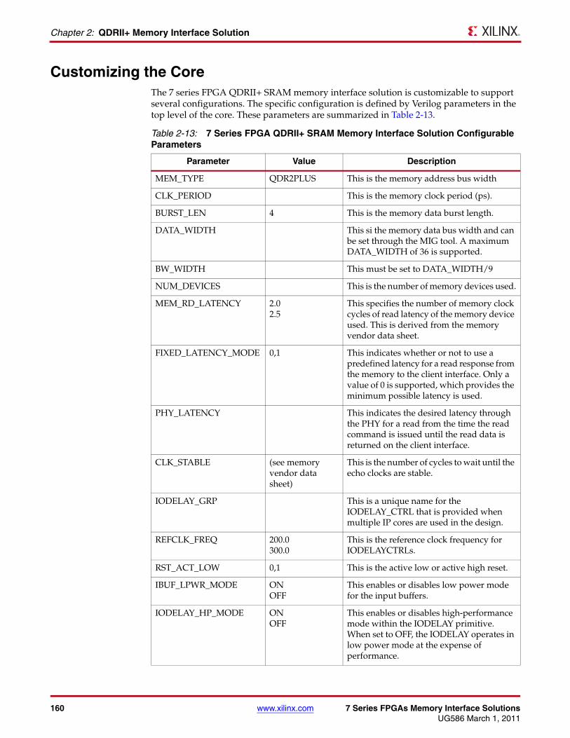
160 www.xilinx.com 7 Series FPGAs Memory Interface SolutionsUG586 March 1, 2011
Chapter 2: QDRII+ Memory Interface Solution
Customizing the CoreThe 7 series FPGA QDRII+ SRAM memory interface solution is customizable to support several configurations. The specific configuration is defined by Verilog parameters in the top level of the core. These parameters are summarized in Table 2-13.
Table 2-13: 7 Series FPGA QDRII+ SRAM Memory Interface Solution Configurable Parameters
Parameter Value Description
MEM_TYPE QDR2PLUS This is the memory address bus width
CLK_PERIOD This is the memory clock period (ps).
BURST_LEN 4 This is the memory data burst length.
DATA_WIDTH This si the memory data bus width and can be set through the MIG tool. A maximum DATA_WIDTH of 36 is supported.
BW_WIDTH This must be set to DATA_WIDTH/9
NUM_DEVICES This is the number of memory devices used.
MEM_RD_LATENCY 2.02.5
This specifies the number of memory clock cycles of read latency of the memory device used. This is derived from the memory vendor data sheet.
FIXED_LATENCY_MODE 0,1 This indicates whether or not to use a predefined latency for a read response from the memory to the client interface. Only a value of 0 is supported, which provides the minimum possible latency is used.
PHY_LATENCY This indicates the desired latency through the PHY for a read from the time the read command is issued until the read data is returned on the client interface.
CLK_STABLE (see memory vendor data sheet)
This is the number of cycles to wait until the echo clocks are stable.
IODELAY_GRP This is a unique name for the IODELAY_CTRL that is provided when multiple IP cores are used in the design.
REFCLK_FREQ 200.0300.0
This is the reference clock frequency for IODELAYCTRLs.
RST_ACT_LOW 0,1 This is the active low or active high reset.
IBUF_LPWR_MODE ONOFF
This enables or disables low power mode for the input buffers.
IODELAY_HP_MODE ONOFF
This enables or disables high-performance mode within the IODELAY primitive. When set to OFF, the IODELAY operates in low power mode at the expense of performance.
7 Series FPGAs Memory Interface Solutions www.xilinx.com 161UG586 March 1, 2011
Design Guidelines
Design Guidelines
Design RulesMemory types, memory parts, and data widths are restricted based on the selected FPGA, FPGA speed grade, and the design frequency. The final frequency ranges are subject to characterization results.
Trace Length RequirementsTrace lengths described here are for high-speed operation and can be relaxed depending on the application’s target bandwidth requirements. The package delay should be included when determining the effective trace length. These internal delays can be found
INPUT_CLK_TYPE DIFFERENTIAL SINGLE_ENDED
This parameter indicates whether the system uses single-ended or differential system clocks/reference clocks. Based on the selected CLK_TYPE, the clocks must be placed on the correct input ports. For differential clocks, sys_clk_p/sys_clk_n must be used. For single-ended clocks, sys_clk must be used.
DIFF_TERM TRUEFALSE
This parameter indicates whether differential or non-differential termination is required for the system clock inputs.
CLKFBOUT_MULT_F This is the MMCM voltage-controlled oscillator (VCO) multiplier. It is set by the MIG tool based on the frequency of operation.
CLKOUT_DIVIDE This is the VCO output divisor for fast memory clocks. This value is set by the MIG tool based on the frequency of operation.
DIVCLK_DIVIDE This is the MMCM VCO divisor. This value is set by the MIG tool based on the frequency of operation.
SIM_BYPASS_INIT_CAL SKIPFASTNONE
This simulation only parameter is used to speed up simulations.
DEBUG_PORT ON, OFF Turning on the debug port allows for use with the Virtual I/O (VIO) of the ChipScope analyzer. This allows the user to change the tap settings within the PHY based on those selected though the VIO. This parameter is always set to OFF in the sim_tb_top module of the sim folder, because debug mode is not required for functional simulation.
Table 2-13: 7 Series FPGA QDRII+ SRAM Memory Interface Solution Configurable Parameters (Cont’d)
Parameter Value Description
162 www.xilinx.com 7 Series FPGAs Memory Interface SolutionsUG586 March 1, 2011
Chapter 2: QDRII+ Memory Interface Solution
using the Pinout and Area Constraints Editor (PACE) tool. These rules indicate the maximum electrical delays between QDRII+ SRAM signals:
• The maximum electrical delay between any bit in the data bus, D, and its associated K/K# clocks should be ±15 ps.
• The maximum electrical delay between any Q and its associated CQ/CQ# should be ±15 ps.
• The maximum electrical delay between any address and control signals and the corresponding K/K# should be ±50 ps.
• There is no relation between CQ and the K clocks. K should be matched with D, and CQ should be matched with Q (read data).
Pinout Requirements7 series FPGAs are designed for very high performance memory interfaces, and certain rules must be followed to use the QDRII+ physical layer. 7 series FPGAs have dedicated logic for each byte group. Four byte groups are available in each 50- pin bank. Each 50-pin bank consists of four byte groups that contain 1 DQS Clock capable I/O pair and ten associated I/Os. Two pairs of Multi-region Clock capable I/O (MRCC) pins are available in a bank, and are used for placing the read clocks (CQ and CQ#).
In a typical QDRII+ write bank configuration, 9 of these ten I/Os are used for the Write data (D) and one is used for the byte write (BW). The write clocks (K/K#) use one of the DQSCCIO pairs inside the write bank. Within a read bank, the read data are placed on 9 of the 10 I/Os, QVLD placed in any of the read data byte groups and the CQ/CQ# clocks placed in the MRCC_P pins available inside the read bank.
7 series FPGAs have dedicated clock routing for high-speed synchronization that is routed vertically within the I/O banks. Thus, QDRII+ memory interfaces must be arranged in the banks vertically and not horizontally. In addition, the maximum height is three banks.
After generating a core through the MIG tool, the most optimal pin out has been selected for the design. Manual changes through the UCF are not recommended. However, if the UCF needs to be altered, the following rules must be taken into consideration:
• The K/K# clocks should be placed in the same bank as the write data banks. The K/K# clocks also need to be placed on a DQSCCIO pin pair
• Write data (D) is placed such that all signals corresponding to one byte (9 bits) are placed inside a byte group along with their corresponding byte write (BW) signal.
• Read data (Q) should also be arranged in bytes(9-bit wide) within byte groups. It is recommended to keep all the read data generated from a single memory component within a bank.
• Read clocks (CQ and CQ#) need to be placed on the two MRCC_P pins, that are available in each bank, respectively.
• Address/control signals can be placed in byte groups that are not used for write or read data.
• Doff_n signal can be placed on any free I/O available in the banks used for the interface.
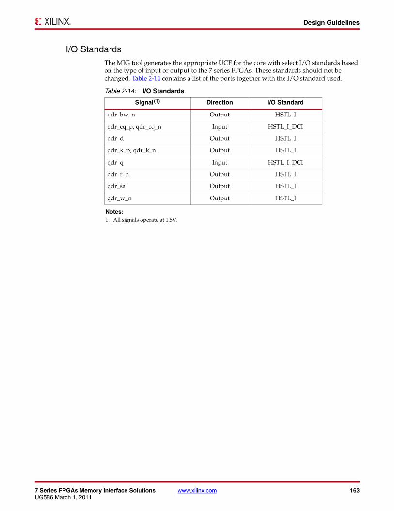
7 Series FPGAs Memory Interface Solutions www.xilinx.com 163UG586 March 1, 2011
Design Guidelines
I/O StandardsThe MIG tool generates the appropriate UCF for the core with select I/O standards based on the type of input or output to the 7 series FPGAs. These standards should not be changed. Table 2-14 contains a list of the ports together with the I/O standard used.
Table 2-14: I/O Standards
Signal(1) Direction I/O Standard
qdr_bw_n Output HSTL_I
qdr_cq_p, qdr_cq_n Input HSTL_I_DCI
qdr_d Output HSTL_I
qdr_k_p, qdr_k_n Output HSTL_I
qdr_q Input HSTL_I_DCI
qdr_r_n Output HSTL_I
qdr_sa Output HSTL_I
qdr_w_n Output HSTL_I
Notes: 1. All signals operate at 1.5V.
164 www.xilinx.com 7 Series FPGAs Memory Interface SolutionsUG586 March 1, 2011
Chapter 2: QDRII+ Memory Interface Solution