7 application of atomic force microscopy and scaling analysis
TRANSCRIPT
8/4/2019 7 Application of Atomic Force Microscopy and Scaling Analysis
http://slidepdf.com/reader/full/7-application-of-atomic-force-microscopy-and-scaling-analysis 1/6
Electrochimica Acta 51 (2006) 2255–2260
Application of atomic force microscopy and scaling analysisof images to predict the effect of current density, temperature and
leveling agent on the morphology of electrolytically produced copper
T. Zhao, D. Zagidulin, G. Szymanski, J. Lipkowski ∗,1
Department of Chemistry, University of Guelph, Guelph, Ont., Canada N1G 2W1
Received 10 May 2005; received in revised form 31 May 2005; accepted 1 June 2005
Available online 12 September 2005
Dedicated to Professor Z. Galus on the occasion of his 70th birthday and in recognition of his contribution to electrochemistry.
Abstract
Atomic force microscopy (AFM) was used to study the morphology of electrodeposited Cu at current densities from 183 to 253 A m−2.
Digital image analysis was employed to parameterize the morphological information encoded in AFM images and to extract information
concerning the mechanism of the electrodeposition reaction. It has been shown how the limiting roughness, δ, the critical scaling length, Lc
and the aspect ratio, 4δ / Lc, vary as a function of the deposition time and electrodeposition conditions, such as temperature, current density
and the amount of organic additives. It has been demonstrated how laboratory experiments of short duration and the scaling analysis of AFM
images can be used to predict roughness of the metal sample after 2 weeks of industrial electrorefining.
© 2005 Elsevier Ltd. All rights reserved.
Keywords: AFM; Surface roughness; Scaling analysis; Copper electrodeposition; Leveling
1. Introduction
Production of many metals, particularly, Ni, Cu, Zn, Ag
and Au involves electrolytic methods based on the metal
electrodeposition reaction. In the past, the metal electrode-
position reaction has been characterized chiefly in terms of
current–voltage or current–time curves. Various models of
the mechanismthatdescribe nucleationand growth under var-
ious constraints, such as diffusion-limited, charge-transfer-
limited and substrate-enhanced growth [1–3] have been pro-posed. However, these models cannot be used to explain and
to predict surface morphology of electrodeposited material.
Spectacular advances in surface imaging techniques, such
as atomicforce microscopy (AFM) or white light interference
microscopy (WLIM) have introduced new tools for the study
∗ Corresponding author.
E-mail address: [email protected] (J. Lipkowski).1 ISE member.
of the morphology of electrodeposited metal. The scaling
analysis of these imagesallows oneto characterizethe growth
of the deposited metal in terms of its surface roughness and
periodicity of surface features in the direction parallel to the
surface (grain sizes). Monitoring evolution of these parame-
ters as a function of the deposition time allows one to predict
the morphology of industrially produced metal with the help
of a laboratory experiment of a relatively short duration [4].
The scaling analysis has beensuccessfully applied to describe
deposition of copper in the presence of organic additives[5,6], deposition of gold and platinum [7], thin films of tin
on steel [8] and electrorefining of nickel [9].
The parameters derived from the scaling analysis also
provide an insight into surface growth mechanisms. Her-
ring [10] proposed that the surface roughness results from
a random material deposition (stochastic roughness), which
is opposed by lateral smoothing processes [4,11–15], such as;
dissolution and re-deposition, surface diffusion and volume
diffusion.
0013-4686/$ – see front matter © 2005 Elsevier Ltd. All rights reserved.
doi:10.1016/j.electacta.2005.06.042
8/4/2019 7 Application of Atomic Force Microscopy and Scaling Analysis
http://slidepdf.com/reader/full/7-application-of-atomic-force-microscopy-and-scaling-analysis 2/6
2256 T. Zhao et al. / Electrochimica Acta 51 (2006) 2255–2260
The objective of this paper is to illustrate the power of
AFM imaging combined with scaling analysis to predict the
morphology of copper electrodeposited at conditions mim-
icking industrial copper electrorefining. We will also show
how to use this technique to optimize the electrorefining
parameters, such as the current density, temperature and con-
centration of organic additives. Modern AFM instrumentsallow imaging of a surface area that is 150 m× 150m
wide and the height of the imaged objects may not exceed
6m. This imposes restrictions on the duration of the
electrolysis, which as a rule should not exceed 10 h. The
deposition time of the industrially produced copper is on the
order of 10 days and the roughness is usually in excess of
10m. The roughness of industrial samples can be measured
with the help of WLIM. We will demonstrate that the AFM
images acquired for a laboratory sample corresponding to
10 min of electrodeposition can be scaled up to predict the
surface morphology after 100 h of electrodeposition (4 days).
The scaled up AFM images will be compared to WLIM
images of industrial copper produced after 4 days of elec-trodeposition. We will show an excellent agreement between
the roughness and morphology displayed by the scaled up
image of a laboratory sample and the image of the industrial
sample. We will provide conclusive evidence that the mor-
phological and topological information obtained by AFM
imaging of copper produced in a laboratory experiment of a
relatively short duration is relevant for industrial production
of copper. Preliminary results of this work were presented in
Ref. [16].
2. Experimental
2.1. Electrodeposition
Copper electrodeposition was carried out using a two-
electrode electrochemical cell consisting of counter (CE)
and working (WE) electrodes. The current density was
controlled by a galvanostat (VersaStat, EG&G Potentio-
stat/Galvanostat). The cathode was a 6 mm diameter copper
slug embedded in resin. It was hand-polished with 600, 800
and then 1200 grade SiC paper, followed by polishing at a
cloth containing 1m alumina powder. The electrode was
then cleaned in an ultra-sonic cleaner to remove alumina, for
a period of 10 min. The polished electrode was placed in a
methanol solution for degreasing.
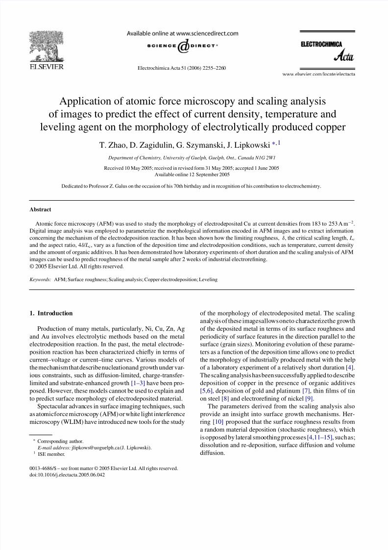
The electrochemical cell is shown schematically in
Fig. 1. Two hundred milliliters of an industrial electrolyte
was circulated between the electrochemical cell and the
reservoir, maintained at the desired operating temperature.
A typical elemental composition of the electrolyte in g/L
was; 40 Cu; 22 Ni; 152 H2SO4; 5.5 Na; 2.5 As; 0.2 Bi. The
volume ratio between the cell and the reservoir was about
1:2.5. To mimic the industrial hydrodynamic regime, the
flow rate of the electrolyte (measured as volume/time) was
equal to the rate used in copper electrorefining, scaled down
Fig. 1. Diagram of the electrochemical cell.
using the ratio of the volume of the industrial tank to the
volume of the experimental cell.
After each deposition, the cathode was rinsed with deion-
ized water. The surface was then imaged by AFM usingdifferent scan sizes. For each plating condition, samples of
electrodeposited metals were collected for a series of elec-
trodeposition times. Morphologyof the electrodeposited cop-
per was investigated at; (i) 54.5, 65 and 76.7 ◦C using current
density 183 A m−2 and (ii) for 213 and 253A m−2 at 65 ◦C.
Glue and tembind (commercial names of a mixture of organic
compounds) were used as leveling agents.
AFM images were captured using Nanoscope E AFM
(Digital Instruments, CA) using silicon nitride tips (Dig-
ital Instruments) which had a nominal spring constant of
0.06 N/m. All images were acquired in height mode, with
both gains ∼3, at scan rates between 7 and 12 Hz. No fil-tering of images was performed other then inherent in the
feedback loop.
The White Light Interference Microscope, model WYKO
NT3300 (Veeco Metrology, Tucson, Arizona) was used to
capture images of the industrial samples using different mag-
nifications (5, 10, 27, 51 and 104).
3. Results
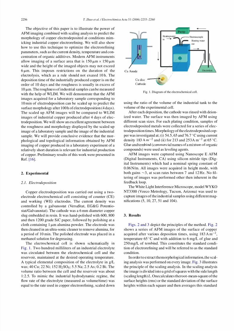
Figs. 2 and 3 depict the principles of the method. Fig. 2
shows a series of AFM images of the surface of copper
acquired after various deposition times, using 183 A m−2,
temperature 65 ◦C and with addition to 6 mg/L of glue and
250 mg/L of tembind. This constitutes the standard condi-
tion of electrorefining and will be referred to as the standard
condition.
In order to extract themorphological information,the scal-
ing analysis was performed on every image. Fig. 3 illustrates
the principle of the scaling analysis. In the scaling analysis
the image is divided into a grid of squares with the side length
(scaling length) L. Onecalculates theroot-mean-square of the
surface heights (rms) or the standard deviation of the surface
heights within each square and then averages this standard
8/4/2019 7 Application of Atomic Force Microscopy and Scaling Analysis
http://slidepdf.com/reader/full/7-application-of-atomic-force-microscopy-and-scaling-analysis 3/6
T. Zhao et al. / Electrochimica Acta 51 (2006) 2255–2260 2257
Fig. 2. AFM images of electrodeposited copper from the solution with
6 mg/L of glue and 250mg/L of tembind at 183A m−2 and at 65 ◦C for
the following deposition times: (a) 0.5 min, (b) 1 min, (c) 2 min, (d) 3 min,
(e) 5 min and (f) 10 min.
deviation over all squares to determine (ξ L) defined as [4,12]:
ξL = [H (x, y) − H (x, y)]2. (1)
The calculation is repeated using another grid of squares
with a different value of the scaling length L and then L is
plotted versus L in logarithmic coordinates. In Eq. (1), H ( x, y)
is the height at the point x, y at the surface, measured with
respect to an arbitrary reference plane.
Fig. 3 shows the log ξ L versus log L plots for four sam-
ples corresponding to different deposition times. For larger
values of the length scale L, the parameter ξ L attains a limit-
ing roughness (δ). The presence of a plateau at the log ξ L
versus log L plots indicates that for a sufficiently large Lthe measured roughness parameter becomes independent of
the scaling length. The scaling theory predicts that the time
dependence of the limiting roughness, is described by:
δ ∝ t β (2)
where β is the growth exponent. The growth exponent may
be easily determined from the slope of the log δ versus log t
plot.
At lower values of the length scale, log ξ L varies in a lin-
ear fashion as a function of log L. In fact, the scaling theory
predicts that in this range:
ξL ∝ Lα (3)
where α is the static exponent and its value should be inde-
pendent of the electrolysis time. The magnitude of parameter
α reveals the dominant mechanism of the surface growth. The
static exponent is related to the coefficient n = 2(α+ 1), that
can be independently determined from the spectral power
density analysis of the images (Fourier transform analysis of
the image). The parameter n = 4 indicates that the deposition
is controlled by surface diffusion while n = 3 indicates that
the smoothing of the surface is due to the so called volume
flow which can be identified as the progressive nucleation
mechanism.The characteristic length L at which the surface rough-
ness attains the limiting value is called the critical scaling
length ( Lc). The critical scaling length measures periodicity
of surface features in the direction parallel to the surface.
Fig. 3. Representative plot of the standard deviation of the surface height, ξ L as a function of the scale length for several growth times. The plateau in the ξ L vs.
L curves defines the root mean square (rms) limiting roughness δ. The scale length L corresponding to the knee in the curves is the critical scaling length, Lc.
Both δ and Lc increase with the deposition time. The inset shows standard log–log plot of Lc, δ and 4δ / Lc vs. time used to determine the roughness exponent
1/ z, the dynamic exponent β and the aspect ratio (optical roughness) exponent γ .
8/4/2019 7 Application of Atomic Force Microscopy and Scaling Analysis
http://slidepdf.com/reader/full/7-application-of-atomic-force-microscopy-and-scaling-analysis 4/6
2258 T. Zhao et al. / Electrochimica Acta 51 (2006) 2255–2260
Table 1
Values of the scaling analysis parameters describing the morphology of electrodeposited copper at investigated conditions
Experimental variable Condition 4δ / Lc ct γ (m) δ at β (m) Lc bt 1/ z (m) α n
Temperature (& 183 A m−2 and 6 mg/L glue) 54.5 ◦C 0.42t −0.03 0.097t 0.35 0.959t 0.38 0.78 4.0
65.0 ◦C 0.61t −0.05 0.130t 0.34 0.869t 0.40 0.80 3.9
76.7 ◦C 0.59t −0.13 0.152t 0.35 1.030t 0.44 0.66 3.9
Current density (& 65.0 ◦C) 213 A m−2
0.34t
0.03
0.088t
0.40
1.031t
0.36
0.73 3.7253Am−2 0.51t 0.01 0.108t 0.40 0.869t 0.40 0.77 4.1
Glue concentration (& 183A m−2 and 65 ◦C) 3 mg/L 0.52t −0.03 0.139t 0.31 1.090t 0.34 0.78 3.9
9 mg/L 0.56t −0.11 0.118t 0.35 0.829t 0.44 0.73 3.9
The theory predicts that Lc depends on time according to the
scaling law:
Lc ∝ t 1/z (4)
where 1/ z is the roughness exponent. The ratio of 4δ / Lc is
the aspect ratio that is a measure of the ratio of the height to
the width of a periodic feature on a corrugated surface (for
example, ratio of the grain height to the grain width). Thedependence of the aspect ratio on time is described by:
4δ
Lc∝ t γ (5)
where γ is the optical roughness exponent. The time depen-
dence of δ, Lc and 4δ / Lc is shown in the inset to Fig. 3. The
advantage of the scaling analysis is that the mechanism of
growth and the evolution of the surface morphology with
the electrodeposition time may be described in terms of four
exponents α, β, 1/ z and γ . The exponent α provides infor-
mation concerning the mechanism of surface growth, while
exponents: β, 1/ z and γ show how the height, width and theaspect ratio of surface features change with the deposition
time. The values of parameters determined from the scaling
analysis are reported in Table 1.
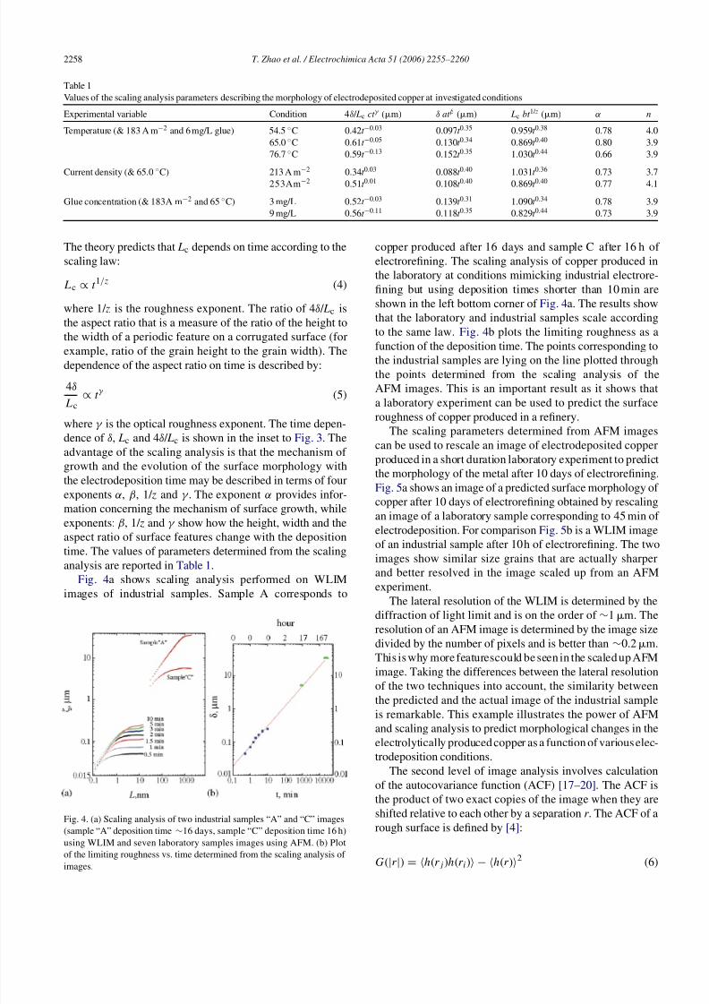
Fig. 4a shows scaling analysis performed on WLIM
images of industrial samples. Sample A corresponds to
Fig. 4. (a) Scaling analysis of two industrial samples “A” and “C” images
(sample “A” deposition time ∼16 days, sample “C” deposition time 16 h)
using WLIM and seven laboratory samples images using AFM. (b) Plot
of the limiting roughness vs. time determined from the scaling analysis of
images.
copper produced after 16 days and sample C after 16 h of
electrorefining. The scaling analysis of copper produced in
the laboratory at conditions mimicking industrial electrore-
fining but using deposition times shorter than 10 min are
shown in the left bottom corner of Fig. 4a. The results show
that the laboratory and industrial samples scale according
to the same law. Fig. 4b plots the limiting roughness as a
function of the deposition time. The points corresponding tothe industrial samples are lying on the line plotted through
the points determined from the scaling analysis of the
AFM images. This is an important result as it shows that
a laboratory experiment can be used to predict the surface
roughness of copper produced in a refinery.
The scaling parameters determined from AFM images
can be used to rescale an image of electrodeposited copper
produced in a short duration laboratory experiment to predict
the morphology of the metal after 10 days of electrorefining.
Fig. 5a shows an image of a predicted surface morphology of
copper after 10 days of electrorefining obtained by rescaling
an image of a laboratory sample corresponding to 45 min of
electrodeposition. For comparison Fig. 5b is a WLIM imageof an industrial sample after 10h of electrorefining. The two
images show similar size grains that are actually sharper
and better resolved in the image scaled up from an AFM
experiment.
The lateral resolution of the WLIM is determined by the
diffraction of light limit and is on the order of ∼1m. The
resolution of an AFM image is determined by the image size
divided by the number of pixels and is better than ∼0.2m.
This is why more featurescould be seen in the scaled up AFM
image. Taking the differences between the lateral resolution
of the two techniques into account, the similarity between
the predicted and the actual image of the industrial sampleis remarkable. This example illustrates the power of AFM
and scaling analysis to predict morphological changes in the
electrolytically produced copper as a function of various elec-
trodeposition conditions.
The second level of image analysis involves calculation
of the autocovariance function (ACF) [17–20]. The ACF is
the product of two exact copies of the image when they are
shifted relative to each other by a separation r . The ACF of a
rough surface is defined by [4]:
G(|r|) = h(rj)h(ri) − h(r)2 (6)
8/4/2019 7 Application of Atomic Force Microscopy and Scaling Analysis
http://slidepdf.com/reader/full/7-application-of-atomic-force-microscopy-and-scaling-analysis 5/6
T. Zhao et al. / Electrochimica Acta 51 (2006) 2255–2260 2259
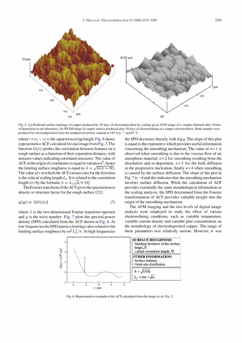
Fig. 5. (a) Predicted surface topology of copper produced by 10 days of electrodeposition by scaling up an AFM image of a sample obtained after 10 min
of deposition in our laboratory; (b) WLIM image of copper surface produced after 10 days of electrorefining in a copper electrorefinery. Both samples were
produced by electrodeposition from the standard electrolyte solution at 183 A m−2 and 65 ◦C.
where r = |r j − r i| is the separation or lag length. Fig. 6 shows
representative ACF calculated for one image from Fig. 2.The
function G(|r |) probes the correlation between features on a
rough surface as a function of their separation distance, with
nonzero values indicating correlated structures. The value of
ACF at the origin of coordinates is equal to varianceδ2, hence
the limiting surface roughness is equal to: δ = √ G(|r = 0|).
The value of r at which the ACF crosses zero for the first time
is the critical scaling length Lc. It is related to the correlation
length (σ ) by the formula; σ = Lc√ α/π [4].
TheFourier transform of the ACF gives the spectral power
density or structure factor for the rough surface [21]:
g(|q|) ≡ [G(|r|)] (7)
where is the two-dimensional Fourier transform operator
and q is the wave number. Fig. 7 plots the spectral power
density (SPD) calculated from the ACF shown in Fig. 6. At
low frequencies the SPD attains a limiting value related to the
limiting surface roughness by αδ2L2c/π. At high frequencies
the SPD decreases linearly with log q. The slope of this plot
is equal to the exponent n which provides useful information
concerning the smoothing mechanism. The value of n = 1 is
observed when smoothing is due to the viscous flow of an
amorphous material; n = 2 for smoothing resulting from the
dissolution and re-deposition, n = 3 for the bulk diffusion
or the progressive nucleation, finally n = 4 when smoothing
is caused by the surface diffusion. The slope of the plot in
Fig. 7 is∼
4 and this indicates that the smoothing mechanism
involves surface diffusion. While the calculation of ACF
provides essentially the same morphological information as
the scaling analysis, the SPD determined from the Fourier
transformation of ACF provides valuable insight into the
origin of the smoothing mechanism.
The AFM imaging and the two levels of digital image
analysis were employed to study the effect of various
electrorefining conditions, such as variable temperature,
variable current density and variable glue concentration on
the morphology of electrodeposited copper. The range of
these parameters was relatively narrow. However, it was
Fig. 6. Representative example of the ACF calculated from the image (e) in Fig. 2.
8/4/2019 7 Application of Atomic Force Microscopy and Scaling Analysis
http://slidepdf.com/reader/full/7-application-of-atomic-force-microscopy-and-scaling-analysis 6/6
2260 T. Zhao et al. / Electrochimica Acta 51 (2006) 2255–2260
Fig.7. Representative exampleof theSPD calculatedfrom theACF in Fig. 6.
Predominant smoothing mechanism: viscous flow (n = 1), evaporation and
condensation (n = 2), bulk diffusion (n = 3) and surface diffusion (n =4).
typical for a change that may take place during industrialcopper electrorefining. Table 1 describes the morphology of
copper, electrodeposited at these experimental conditions,
in terms of parameters determined from the scaling analysis
of the AFM images. Columns one and two describe the
experimental condition. Columns three to five report values
of the surface roughness, the critical length and the aspect
ratio at any value of deposition time. These numbers may
be used to calculate the surface roughness and the width of
the surface features (grains) at a desired time of the electro-
refining.
The last two columns in Table 1 report the values of the
static scaling coefficient α and the smoothing coefficient n.We recall that according to the theory n = 2(α+ 1). The val-
ues of n determined from the SPD were approximately equal
to 4 under all the experimental conditions. The values of n
calculated from α were on the order of 3.5. These numbers
indicate that surface diffusion was the predominant smooth-
ing mechanism [4].
The following predictions can be made with the help
of parameters listed in Table 1. The surface roughness and
the critical length increase with temperature. However, the
roughness increases faster with time than the critical length.
At a longer electrolysis time, the aspect ratio of grains in
copper produced at 76.7◦ will be smaller than at 54.5◦. The
surface produced at the highest temperature will be more
leveled and the deposit will consist of larger grains. There
is surprisingly little effect of the current density on the mor-
phology of electrodeposited copper. Parameters β, 1/ z and γ
change little with the current density. In addition γ is close to
zero indicating that the aspect ratio changes very little with
the deposition time. The experiments carried out using solu-
tions with glue concentrations of 3, 6 and 9 mg/L show that
the surface roughness decreasesbut the critical scaling length
increases when more glue is present in the electrolyte. This
causes a significant decrease of the aspect ratio. Clearly, glue
acts as a typical leveling agent. Copper with a smoother and
more leveled surface is produced when the glue content in
the electrolyte increases.
4. Summary and conclusions
Atomic force microscopy hasbeen shown to be a powerful
tool for studying surface morphologies of electrodepositedmetals. The digital image analysis allows one to encode
the morphological information contained in the image of
electrodeposited metal in the magnitude of a few numerical
parameters. These parameters may then be used to predict
the surface morphology of a metal produced by prolonged
electrolysis, from an experiment of short duration.
We have applied this method to investigate the effect of
temperature, current density and glue concentration on the
morphology of electrodeposited copper. A relatively narrow
range of these parameters, typical for a change that may take
place during copper electrorefining, were investigated. The
results of these experiments may help the refinery to eitheroptimize the electrolytic production of copper or to predict
the effect of an unexpected change of the electrodeposition
conditions.
References
[1] E. Bosco, S.K. Rangarajan, J. Electroanal. Chem. 134 (1982) 213.
[2] J.O’M. Bockris, G.A. Razumny, Fundamental Aspects of Electro-
crystallization, Plenum Press, NY, 1967.
[3] B. Scharifker, G. Hills, Electrochim. Acta 28 (1983) 879.
[4] W.M. Tong, R.S. Williams, Annu. Rev. Phys. Chem. 45 (1994) 401.
[5] W.U. Schmidt, R.C. Alkire, A.A. Gewirth, J. Electrochem. Soc. 143
(1996) 3122.
[6] H. Iwasaki, T. Yoshinobu, Phys. Rev. B 48 (1993) 8282.
[7] J.M. Gomez-Rodriguez, A.M. Baro, L. Vazquez, R.C. Salvarezza,
J.M. Vara, J. Phys. Chem. 96 (1992) 347.
[8] T. Jiang, N. Hall, A. Ho, S. Morin, Thin Solid Films 471 (2005)
76–85.
[9] G. Szymanski, M. Pogoda, B. Campbell, J. Lipkowski, Proceed-
ings of the 27th Annual Hydrometallurgical Meeting of CIM
Nickel–Cobalt, Sudbury, 1997.
[10] C. Herring, J. Appl. Phys. 21 (1950) 301.
[11] D.D. Vvedensky, A. Zangwill, C.N. Luse, M.R. Wilby, Phys. Rev.
E 48 (1993) 852.
[12] A.-L. Barabasi, H.E. Stanley, Fractal Concepts in Surface Growth,
Cambridge University Press, New York, 1995.
[13] E.A. Eklund, E.J. Synder, R.S. Williams, Surf. Sci. 285 (1993) 157.
[14] D.G. Stearns, Appl. Phys. Lett. 62 (1993) 1745.[15] G. Palasantzas, J. Krim, Phys. Rev. Lett. 73 (1994) 3564.
[16] G. Szymanski, M. Dymarska, T. Zhao, J. Lipkowski, Proceedings
of the 31st Annual Hydrometallurgy Meeting, Canadian Institute of
Mining, Metallurgy and Petroleum (CIM), Toronto, Ont., Canada,
August 26–29, 2001, p. 375.
[17] H. Iwasaki, T. Yoshinobu, Phys. Rev. B 48 (1993) 8282.
[18] G. Kahanda, X. Zou, R. Farre, P. Wong, Phys. Rev. Lett. 68 (1992)
3741.
[19] D.P. Barkey, R.H. Muller, C. Tobias, J. Electrochem. Soc. 136 (1989)
2199.
[20] P. Garic, D. Barkey, E.B. Jacob, E. Bochner, N. Broxholm, B. Miller,
B. Orr, R. Zamir, Phys. Rev. Lett. 69 (1989) 2703.
[21] J.M. Elson, H.E. Bennett, J.M. Bennett, in: R.R. Shannon, J.C. Wyant
(Eds.), Applied Optics and Optical Engineering, vol. 8, 1979, p. 191.